
RadioProcessor™ Owner’s Manual SpinCore Technologies, Inc.
RadioProcessor™
Owner’s Manual
SpinCore Technologies, Inc.
http://www.spincore.com
RadioProcessor
Congratulations and thank you for choosing a design from
SpinCore Technologies, Inc.
We appreciate your business!
At SpinCore we try to fully support the needs of our customers. If you
are in need of assistance, please contact us and we will strive to provide
the necessary support.
© 2009-2014 SpinCore Technologies, Inc. All rights reserved.
SpinCore Technologies, Inc. reserves the right to make changes to the product(s) or information herein without notice.
RadioProcessor™, PulseBlaster™, SpinCore, and the SpinCore Technologies, Inc. logos are trademarks of SpinCore Technologies, Inc.
All other trademarks are the property of their respective owners.
SpinCore Technologies, Inc. makes every effort to verify the correct operation of the equipment. This equipment version is not
intended for use in a system in which the failure of a SpinCore device will threaten the safety of equipment or person(s).
www.spincore.com
2014-09-02
2
RadioProcessor
Table of Contents
I. Introduction........................................................................................... 5
Product Overview .......................................................................................................... 5
System Architecture ......................................................................................................6
Example Application...................................................................................................... 7
Specifications................................................................................................................. 9
Transmitter Output Level.............................................................................................10
II. Board Installation............................................................................... 11
Installing the RadioProcessor ....................................................................................11
Testing the RadioProcessor........................................................................................11
III. Example Single-Pulse NMR Experiment......................................... 13
Precompiled C Programs with Batch File Control....................................................13
Tips on obtaining data using singlepulse_nmr ........................................................ 14
Graphical User Interfaces............................................................................................15
IV. Creating Custom Pulse Programs................................................... 16
Controlling the RadioProcessor with SpinAPI .......................................................... 16
DDS (Frequency and Phase) Registers......................................................................16
Acquisition Parameters................................................................................................17
Timing and Flow Control Parameters.........................................................................18
Triggering...................................................................................................................... 19
Retrieving data from the board................................................................................... 20
V. Connecting to the RadioProcessor.................................................. 21
PCI RadioProcessor Boards Connector Information ............................................... 21
BNC Connectors......................................................................................................21
www.spincore.com
2014-09-02
3
RadioProcessor
Long IDC Headers................................................................................................... 22
HW Trigger/Reset Header....................................................................................... 23
USB RadioProcessor Boards Connector Information ..............................................23
Power Connectors................................................................................................... 24
RF Connectors.........................................................................................................25
Digital Output Connector......................................................................................... 25
Header JP302 (HW Trigger/Reset)......................................................................... 26
USB RadioProcessor Board in a Single-bay Enclosure Connector Information . .27
Power Connector..................................................................................................... 28
RF Connectors.........................................................................................................28
Digital Output Connector......................................................................................... 29
HW Trigger/Reset.................................................................................................... 29
Appendix I: Using the Undersampling Capabilities of the
RadioProcessor - 70 MHz IF Application................................................. 30
Appendix II: Arbitrary Waveform Generation....................................... 36
Appendix III: RadioProcessor NMR Interface for MATLAB ................39
Overview of SpinCore MATLAB GUI Interface...........................................................39
General Features:....................................................................................................39
Sample Screenshots................................................................................................39
Appendix IV: RadioProcessor NMR Interface for LabVIEW ...............43
Overview of SpinCore LabVIEW GUI Interface..........................................................43
Appendix V: Miscellaneous Functionality............................................ 45
Appendix VI: CYCLOPS Control.......................................................... 48
Appendix VII: RadioProcessor Firmware Designs.............................51
Related Products and Accessories...................................................... 52
Contact Information............................................................................... 52
Document Information........................................................................... 52
www.spincore.com
2014-09-02
4
RadioProcessor
I. Introduction
Product Overview
The RadioProcessor™ is a general purpose radio frequency (RF) excitation and broadband data
acquisition system. The RadioProcessorTM can serve as a complete system for Nuclear Magnetic Resonance
(NMR) or Nuclear Quadrupole Resonance (NQR) experiments with spectrometer frequencies from 0 to 100
MHz (certain restrictions apply, vide infra). The system integrates SpinCore’s high-performance
PulseBlaster™ timing engine for agile control of internal system components as well as TTL pulse/pattern
generation for control of any external hardware.
The RadioProcessor™
• Integrates excitation and acquisition components onto a single PCI or USB card.
• Directly captures and digitally demodulates IF/RF signals using quadrature detection. The desired
baseband bandwidth is user definable through software filters.
• Generates completely formed RF excitation pulses as well as high resolution digital control signals.
• Supports 2 analog I/O channels and 4 digital output channels.
• Maintains signal coherence between excitation and acquisition systems at all frequencies.
• Autonomously signal-averages the baseband data between multiple acquisitions.
• Saves data in several different formats. Currently supported file formats are ASCII, Felix, and
JCAMP-DX 5.0.
This unique digital system is housed on a small form factor printed-circuit board available in either PCI or
USB format, providing users with a compelling price/size/performance proposition unmatched by any other
device on the market today. The RadioProcessorUSB board is available assembled into a single-bay
enclosure. Please contact SpinCore for more details.
www.spincore.com
2014-09-02
5
RadioProcessor
System Architecture
Figure 1, below, presents the architecture of the RadioProcessor™. The RadioProcessor consists of three
major components: the data acquisition core, the excitation core, and the PulseBlaster timing engine which
provides high-resolution timing control for the entire system.
Figure 1: RadioProcessor Architecture. The master clock oscillator signal is derived from an on-chip PLL
circuit typically using a 50 MHz on-board reference clock.
The acquisition core captures an incoming RF signal using a high-speed, high resolution Analog to Digital
converter (ADC). This signal is then demodulated digitally using quadrature detection and filtered to reduce
the signal to baseband. The detection and filtering system is highly configurable and can easily be customized
by the user for a wide variety of applications. The baseband signal can then be averaged with previous data
acquisition scans and is stored in an internal RAM. This data is then available to be retrieved onto the host
computer at the user's convenience.
The excitation core can produce both RF Analog signals as well as digital outputs. The RF output is
generated using an internal DDS (Direct Digital Synthesis) core, and can generate frequencies from DC up to
half the DDS clock. The generated signal is converted to the Analog output by an on board digital-to-analog
converter (DAC) This DDS core also drives the detection of the acquisition core, so signal coherence is
maintained between acquisition and excitation cores. High resolution programmable digital outputs are also
available for use in controlling external hardware.
At the heart of the system is the PulseBlaster™ pulse/pattern generator timing core, which uses a robust
instruction set designed to allow the creation of complex pulse sequences with ease. This timing core controls
all aspects of the systems functionality, such as triggering data acquisition, controlling the frequency and
gating RF output, etc. The digital outputs are also controlled with this core. Six digital outputs are available by
default, and more are possible if some features of the excitation and acquisition cores are not used. The
PulseBlaster™ core utilizes an 80-bit Very Long Instruction Word (VLIW) which enables dynamic timing
delays for each instruction. For more information about the PulseBlaster core, please see the PulseBlaster
Manual.
www.spincore.com
2014-09-02
6
RadioProcessor
Example Application
A major application for the RadioProcessor is to serve as an advanced digital NMR/NQR spectrometer.
Using the RadioProcessor, a complete NMR/NQR system can be constructed with the addition of a power
amplifier and a pre-amplifier. An example setup is shown below in Figure 2.
Figure 2: Typical application of the RadioProcessor. By adding a power amplifier and a small-signal preamplifier, a complete NMR/NQR system can be built.
If you are building a system with the RadioProcessor board, SpinCore Technologies Inc. can also supply a
power amplifier, TX/RX switch, and pre-amplifiers, if desired. SpinCore also offers a complete mobile NMR
system, the iSpin-NMR, that can perform NMR/NQR experiments immediately out of the box. Please visit our
website for more details.
www.spincore.com
2014-09-02
7
RadioProcessor
Using a setup as described above with a 10.8 MHz permanent magnet, sample spectrum of a household
cooking oil sample was obtained as shown below. Using only a single scan, a signal to noise ratio of 62 dB
was achieved. The spectral width of the figure below is 60 kHz.
Figure 3: Sample single-scan proton spectrum obtained at 10.8 MHz with the RadioProcessor board and
the system described in the text above.
www.spincore.com
2014-09-02
8
RadioProcessor
Specifications
The RadioProcessor is currently available with a 75 MHz Analog-to-Digital (A/D) sampling clock frequency.
Specifications for this configuration are given below. For information specific to a certain RadioProcessor
firmware revision, see Appendix VII or contact SpinCore Technologies, Inc.
Parameter
Analog Input
Min
Max
Units
80
MHz
14
bits
Input Voltage Range (peak-peak)
1.13
V
Input Frequency Range
100
MHz
A/D Sampling Frequency
Typ
75
(3)
A/D Sampling Precision
Analog Output
D/A Sampling Rate
300
D/A Sampling Precision
14
Output Voltage Range (peak-peak)
1.2
Phase resolution
0.09
(8)
Frequency resolution
Digital Output
MHz
Number of Digital Outputs
.28(6)
4
6
bits
V
deg.
Hz
24
(2)
Logical 1 output voltage
3.3(1)
V
Logical 0 output voltage
0
V
Output drive current
25
mA
Rise/Fall time
<1
ns
Digital Input
Logical 1 Input voltage
1.7
4.1
V
(HW_Trig, HW_Reset)
Logical 0 Input voltage
-0.5
0.7
V
Data acquisition
Spectral width (SW) of acquired data 0.28 Hz(10)
# Complex points
Pulse Program
10 MHz(7)
8192(9)
16k
# of Instruction words
Pulse resolution
Pulse length
1024
13.3
(4)
66.6 ns
(5)
words
ns
693 days
Table 1: Product Specifications.
Notes
(1): This is the value seen without using termination. When the line is terminated with 50Ω, the output voltage will be slightly lower.
(2): Custom designs are available. Please contact SpinCore if you require more digital outputs (or DDS registers).
(3): If the signal to be detected is very close to ¼ of the sampling rate, there will be problems with aliasing during the detection
process. To alleviate this problem, a slightly higher or lower clock speed can be used.
(4): Pulse resolution equals one clock period of the master clock oscillator.
(5): Minimum pulse width is five clock periods of the master clock oscillator. Maximum pulse width is 2^52 clock periods of the
master clock oscillator.
(6): Frequency resolution is .30 Hz when using a 80 MHz clock.
(7): This number is dependent on the A/D clock frequency (i.e., A/D clock frequency divided by 8). NOTE: when acquiring data
directly from A/D, the spectral width is ½ the A/D clock frequency.
(8): Analog output voltage is factory adjustable up to 4V. See Transmitter Output Level section on the next page for more
information.
(9): Fewer points may be observed, however, the number of points retrieved from board memory must be a multiple of 8k.
(10): This value is with the FIR Enabled. With FIR Bypassed, min SW is 72 Hz. Some older designs have a min SW of 4.5 Hz (1.2
kHz with FIR Enabled).
www.spincore.com
2014-09-02
9
RadioProcessor
Transmitter Output Level
Voltage (volts pk-pk on 50 Ohms)
There are currently two different options for RadioProcessor transmitter output voltage. The standard gain
RadioProcessor has an output voltage of one volt peak-to-peak at 10 MHz, with a 3 dB bandwidth of about 85
MHz. The high gain transmitter output amplifier has a maximum output voltage of about 3.75 Volts peak-topeak, with a 3dB bandwidth of about 21 MHz, while covering the same frequency range as the standard gain
board. Figure 4 below shows the transmitter output voltage vs. frequency plot for the two RadioProcessor
options. Please contact SpinCore for more information.
4
3.5
3
2.5
High Gain
Standard Gain
2
1.5
1
0.5
0
0
20
40
60
80
100
120
Frequency (MHz)
Figure 4: RadioProcessor transmitter output voltage vs. output frequency.
The dotted line represents the standard gain transmitter output amplifier, and the
solid line represents the high gain transmitter output amplifier. The voltage
values are for 50 Ohm load impedance. The 0 dB (1 mW, 0.63 Vpp on 50 Ohm)
output value for both transmitter amplifiers occurs at approximately 90 MHz.
www.spincore.com
2014-09-02
10
RadioProcessor
II. Board Installation
Installing the RadioProcessor
To install the board you must complete the following steps:
1. Download and install the latest SpinAPI software package on your computer. SpinAPI is available at:
http://www.spincore.com/support/spinapi/.
•
SpinAPI is a custom Application Programming Interface package developed by SpinCore
Technologies, Inc. SpinAPI is designed to be used only with SpinCore Technologies, Inc.
products. SpinAPI can be utilized using C/C++, or graphically (described in Appendices III and
IV).
2. Download and install the latest SpinAPI Examples for your device based on the SpinAPI library. The
Examples are available at: http://spincore.com/CD/spinapi_examples/.
3. Shut down the computer.
4. For the PCI: Insert the RadioProcessor card into an available PCI slot and fasten the PC bracket
securely with a screw.
5. For the USB: Plug one end of the USB cable into the RadioProcessor board and the other end into the
host computer. Next, power the board through the 5-pin DIN-type connector or 6-position Molex-style
connector. We recommend purchasing the RadioProcessorUSB Power Supply, which has the 6-pin
output connector and is pin-compatible with the power connector of the RadioProcessorUSB board.
For more information on powering the RadioProcessor USB board please read Power Connectors in
Section V. Connecting to the RadioProcessor.
•
Warning: Do not connect PEG (PCI Express Graphics) power connectors available in some
computers directly to the 6-position Molex-style power connector. Doing so will cause irreparable
damage to the board. SpinCore Technologies is not liable for any damage caused by this.
6. Turn on the computer.
Now you are ready to run the test programs you downloaded from the SpinAPI Examples. We recommend
running the example programs when you first receive a RadioProcessor device to verify that your device is
functional.
Testing the RadioProcessor
The simplest way to test whether the RadioProcessor has been installed properly and can be controlled as
intended is to run a simple test program. The excite_test program, that is available for download online at:
http://www.spincore.com/support/spinapi/spinapi_examples.shtml, will produce a 1 MHz output on the Analog
Out connector which will turn on for 10 μs and off for 1 ms. This sequence will be repeated indefinitely. To test
the board, run excite_test and observe the Analog Output with an oscilloscope. The 1 MHz sinusoid should
appear as specified by the program.
If using a high input impedance oscilloscope to monitor the RadioProcessor's output, place a resistor that
matches the characteristic impedance of the transmission line in parallel with the coaxial transmission line at
the oscilloscope input. (e.g., a 50 Ω resistor with a 50 Ω transmission line, see Figures 5 and 6 below.). When
using an oscilloscope with an adjustable bandwidth, set the bandwidth to as large as possible. Failure to do
so may yield inaccurate readouts on the oscilloscope.
www.spincore.com
2014-09-02
11
RadioProcessor
Figure 5: Left: BNC T-Adapter and Right: BNC 50 Ohm resistor
Figure 6: BNC T-Adapter on the oscilloscope with coaxial transmission line connected
on the left and BNC 50 Ohm resistor connected on the right, to terminate the line.
Once this behavior has been verified, the user can be confident the board is installed properly and may
move on to evaluation of the acquisition subsystem. If the RadioProcessor is to be used to perform NMR
experiments, the easiest way to do this is to use the provided singlepulse_nmr example program. The
use of this program is described in detail in the next section.
www.spincore.com
2014-09-02
12
RadioProcessor
III. Example Single-Pulse NMR Experiment
Precompiled C Programs with Batch File Control
Several precompiled NMR experiments are included with the SpinAPI Examples (Single-Pulse NMR, Hahn
Echo, and CPMG, for example). The following steps describe how to run the Single-Pulse NMR experiment
with the RadioProcessor board and SpinCore Technologies software:
1. Complete the steps in Section II. Board Installation for Installing the RadioProcessor before
proceeding.
2. Connect the RadioProcessor as shown in Figure 2 (page 7) of this manual. Note that all components
shown in Figure 2 may be purchased from SpinCore Technologies.
3. Create your own working directory somewhere outside of the SpinCore directory and copy the
contents of the SpinCore RadioProcessor directory to your new working directory. The SpinCore
RadioProcessor directory can be found by in the location where you downloaded the RadioProcessor
Examples.
4. Edit the singlepulse_nmr_example.bat batch file by right-clicking and selecting 'edit' and save the
batch file when finished. The parameters of interest for this experiment are described below:
BOARD_NUMBER: Selects which board to program if multiple SpinCore Technologies boards are
connected to your system.
ADC_FREQUENCY: Clock frequency of the board. Always 75 MHz, unless a custom clock is being used as
input to the RadioProcessor.
ENABLE_TX: A 1 enables the transmitter, a 0 disables the transmitter.
ENABLE_RX: A 1 enables the receiver, a 0 disables the receiver.
REPETITION_DELAY: Repetition delay in seconds between scans. See Figure 5.
NUMBER_OF_SCANS: Number of times to repeat the scan and average the results together.
NUMBER_OF_POINTS: Number of complex points to be captured.
SPECTROMETER_FREQUENCY: Spectrometer frequency in MHz.
SPECTRAL_WIDTH: Desired base band spectral width in kHz.
PULSE_TIME: Duration of TX excitation pulse in μs. See Figure 5.
TRANS_TIME: Ringdown time in μs. See Figure 5.
TX_PHASE: Phase of the TX output channel in degrees.
AMPLITUDE: TX output amplitude scaling factor (between 0.0 and 1.0).
SHAPED_PULSE: Uses a 'sinc' shaped pulse for the TX output.
BYPASS_FIR: A 1 bypasses the FIR filter, 0 enables it.
FNAME: File name to save the acquired data in. Data will be saved in ASCII, Felix, and JCAMP formats.
VERBOSE: A 1 enables normal output, a 0 disables normal output and the program outputs nothing.
BLANKING_EN: Enables the TTL blanking feature necessary to control SpinCore Technologies RF Power
Amplifier modules if used with the RadioProcessor in the NMR setup. For more information see the
RF Power Amplifier manual at: http://www.spincore.com/CD/RFPA/RFPA_Manual.pdf
BLANKING_BIT: Specifies which TTL Flags to use for blanking.
BLANKING_DELAY: Delay needed to warm-up the SpinCore RF Power Amplifier prior to the RF pulse.
See Figure 7.
www.spincore.com
2014-09-02
13
RadioProcessor
Blanking
Signal
RF
Output
NMR
Signal
Blanking Delay
Pulse Time
Transient
Time
Acquisition Time
Repetition Delay
Figure 7: General timing diagram of the basic single-pulse sequence (not to scale). A single scan is
performed as follows: A blanking TTL pulse is applied to allow for RF Power Amplifier warm-up (Blanking
Delay), a single RF pulse is applied to the sample for a specified amount of time (Pulse Time). The high
voltage induced on the sample coil is allowed to ring down (Transient Time), after which the Free Induction
Decay (FID) signal is acquired (for length Acquisition time). The sample is then allowed to relax for a time
(Repetition Delay). This scan procedure is then repeated an arbitrary number of times as desired to improve
the signal to noise ratio.
5. Run the singlepulse_nmr_example.bat file by double-clicking. Once the singlepulse_nmr.bat file has
completed, three new files (*.fid, *.jdx, *.txt) will be created in the directory from which the batch file
was executed.
6. Open the Felix file (.fid) in Felix for Windows, or open the .jdx file in any program that supports
JCAMP-DX. An easily parsed text file containing the NMR data will also be generated. For information
on installing and using Felix to view your .fid files, go to
http://www.spincore.com/CD/RadioProcessor/felix/Felix_Instructions.html
Tips on obtaining data using singlepulse_nmr
The ability of this program to capture usable data is highly dependent on entering the correct parameters
for a given NMR setup. It is expected that the user is familiar with how to best specify PULSE_TIME,
TRANS_TIME, TX_PHASE, SPECTROMETER_FREQUENCY, etc. Setting the SPECTRAL_WIDTH,
however, may not immediately be obvious.
If the signal is very short (on the order of microseconds), for example as in NMR with solid samples or with
inhomogeneous magnetic fields, there is ample room in the on board RAM to capture the entire signal with a
very large spectral width (1 MHz or more). Often this is the best approach, even if the signals are near DC
(i. e. near or at spectrometer frequency) and thus do not require a large spectral width to be represented. To
do this, the FIR filter can be bypassed with the BYPASS_FIR parameter to achieve the large spectral width.
This will result in signals being attenuated near the edge of the passband, but this will not matter since the
signal of interest is near DC.
www.spincore.com
2014-09-02
14
RadioProcessor
For longer FID signals, where a smaller spectral width is more useful, the FIR filter may be bypassed as
well. The FIR filter is necessary only for very low spectral widths (on the order of several Hz) when a flat
response is needed over the entire spectrum. Please note that when the FIR is enabled, the spectral width
must be the ADC_FREQUENCY divided by some multiple of 8. If such a value is not specified, the spectral
width will be rounded appropriately. The FIR filter also adds an initial latency to any acquired data that is
dependent on the number of FIR coefficients. These initial points should be discarded. In general, lowering
the spectral width will reduce the noise in the signal.
The source code of the singlepulse_nmr.c program is included in the SpinAPI Examples and is well
commented. Users wishing to create custom programs may refer to this to get the details of how to control the
RadioProcessor.
Graphical User Interfaces
In addition to the Single Pulse NMR code included with SpinAPI, graphical user interfaces have been
created for use with MATLAB and LabVIEW. Please see Appendices III and IV for sample screenshots, or
visit the following links for further information.
MATLAB: http://www.spincore.com/support/RadioProcessor/MATLAB/
LabVIEW: http://www.spincore.com/support/PBLV/RP.shtml
www.spincore.com
2014-09-02
15
RadioProcessor
IV. Creating Custom Pulse Programs
Controlling the RadioProcessor with SpinAPI
SpinAPI is a control library which allows programs to be written to communicate with the RadioProcessor
board. The most straightforward way to interface with this library is with a C/C++ program, and the API
definitions are described in this context. However, virtually all programming languages and software
environments (including software such as LabVIEW and MATLAB) provide mechanisms for accessing the
functionality of standard libraries such as SpinAPI.
For more information on using SpinAPI functions, please download the RadioProcessor Examples available
online at: http://spincore.com/CD/spinapi_examples/.
A reference document for all SpinAPI functions is available online at:
www.spincore.com/CD/spinapi/spinapi_reference
The RadioProcessor is a highly versatile excitation and acquisition system, and as a result there are many
possible approaches to program the board. However, most applications will follow five basic steps:
1. Load the frequency and phase registers with desired values.
2. Specify data acquisition related parameters.
3. Specify all parameters that control the timing of the experiment, i.e., pulse times, delays, etc.
4. Trigger the pulse program. The experiment will then proceed autonomously.
5. Retrieve the captured data from the board at any time without interrupting the acquisition process.
These steps are described in detail below. For each of the steps, the relevant SpinAPI functions are listed
which control the actions needed to perform that particular step.
DDS (Frequency and Phase) Registers
The RadioProcessor contains three DDS channels, two of which are internal and used for digital detection
(cos and sin), and one which drives the digital-to-analog converter (DAC) that forms the TX channel (see
figure 5 below). The frequency and phases of these three channels are controlled by selecting values from a
bank of on-board registers. These registers are typically programmed during board initialization , and then the
pulse program is used to select which register is used at any given time during an experiment. All three
channels share a common frequency, but their phase may be set completely independent of each other. The
number of available registers for each channel is given in the table below*.
Register Bank
Number of registers
Frequency
16
Cos phase (real channel)
4
Sin phase (imaginary channel)
4
TX phase
16
Table 2: DDS Register information.*
Relevant spinapi functions:
pb_start_programming()
*Certain RadioProcessor firmware revisions have different register allocation. For information about a specific RadioProcessor
firmware revision see Appendix VII or contact SpinCore Technologies, Inc. Custom designs with more DDS registers are available.
www.spincore.com
2014-09-02
16
RadioProcessor
pb_set_phase()
pb_set_freq()
pb_stop_programming()
Firmware revision 10-18 supports “on the fly” frequency and phase register programming. Please see
Appendix V for more information.
Acquisition Parameters
The RadioProcessor performs quadrature signal detection, as shown in Figure 8 below. The incoming RF
signal as captured by the ADC is multiplied by the internal cos and sin signals to form the real and imaginary
signal channels respectively. These channels are then filtered and decimated to produce a baseband signal,
which can optionally be averaged with previous scans, and is then stored in the internal ram.
Real Channel
Incoming
Analog
Signal
Filtering
and
Decimation
ADC
Imaginary Channel
cos
DDS
Signal
Averaging
and
Storage
Filtering
and
Decimation
sin
Tx
To Tx Output
Channel
CYCLOPS
Control
Figure 8: Quadrature detection block diagram. The incoming analog signal is digitized and mixed with
the receiver cosine and sine waveforms to create the real and imaginary channels. Those channels are
then filtered and stored in on chip memory for the user to read back. The RadioProcessor's agile control
system allows for all aspects of the data acquisition to be user programmable.
Basic acquisition parameters that need to be set are the desired spectral width of the stored baseband
data, the number of points to capture, and the number of scans that will be performed. Based on these values,
the driver will set the internal acquisition and filtering parameters appropriately. This method of setting up the
acquisition hardware should suffice for many if not most applications. Complete control over all filtering
parameters is possible however, and users wishing to take advantage of this should contact SpinCore
Technologies.
Spectral width: This is the bandwidth of the captured baseband (i.e., after quadrature detection) data.
Number of points: Number of complex basedband (FID) points to capture. This is typically set to the
maximum number of points, although smaller numbers may be used if a lesser number of points is sufficient.
Number of scans: Number of scans that are intended to be taken. The actual number of scans is
determined by the number of times the trigger_scan bit is enabled in the pulse program, but the maximum
number of scans that will be performed needs to be specified here so that the acquisition system can be setup
to avoid overflows.
www.spincore.com
2014-09-02
17
RadioProcessor
Relevant spinapi functions:
pb_set_num_points()
pb_setup_filters()
NOTE: To bypass the Digital Quadrature Detection use the spinapi function: pb_get_data_direct()
Timing and Flow Control Parameters
The RadioProcessor contains an integrated PulseBlaster pulse generation timing core. This timing core
controls all aspects of the systems functionality by setting internal control lines at user specified times. Six
user programmable digital outputs are also available for control of external hardware. The internal control lines
and user programmable outputs are collectively referred to as flags. The pulse program modifies these flags
in a user-defined way to control all aspects of an experiment.
Op-code and Explanation
The PulseBlaster uses a robust instruction set to enable the creation of complex pulse programs with ease.
Each instruction is defined by an opcode which specifies the action of that instruction and an optional
Instruction data (inst_data) field which elaborates on that action. In addition, each instruction specifies the
desired value for the flags, as well as a time delay until the next instruction executes. The “next” instruction is
not necessarily the next sequential instruction, as the instruction set contains branching and looping
instructions which can cause the program to be executed out of sequential order. A list of the available
instructions is given in the table below.
Op Code #
Instruction
0
CONTINUE
1
STOP
2
LOOP
3
END_LOOP
4
JSR
5
RTS
6
BRANCH
7
LONG_DELAY
8
WAIT
Inst_data field
Function
Program execution continues to next
Unused
instruction. This can only be used up to a
delay of 231*13.3ns or about 28 s.
Stop execution of program. All TTL
values remain from previous instruction, and
analog outputs may turn off (1) . It is
Unused
recommended to provide a termination
command to deactivate outputs before a
STOP.
Number of desired loops.
Specify beginning of a loop. Execution
This value must be greater continues to next instruction. Data used to
than or equal to 1.
specify number of loops
Specify end of a loop. Execution returns
Address of beginning of
to begging of loop and decrements loop
loop
counter.
Address of first subroutine
Program execution jumps to beginning of
instruction
a subroutine
Program execution returns to instruction
Unused
after JSR was called
Program execution continues at specified
Address of instruction to
instruction. This behaves like the goto
skip to
statement found in many programming
languages
For long interval instructions (intructions
Number of desired loops.
with a delay over 28 s). Data field specifies
This value must be greater
a multiplier of the delay field. Execution
than or equal to 2.
continues to next instruction
Unused
Program execution pauses and waits for
a software or hardware trigger to resume it.
The latency between a trigger occurring and
(1) On RadioProcessor boards with firmware versions 10-13 and 10-14, both analog and TTL outputs return to ground when a
STOP command is encountered.
www.spincore.com
2014-09-02
18
RadioProcessor
the program resuming is the time used as
the delay for the wait instruction plus a fixed
time of 6 clock cycles.
Table 3: PulseBlaster instructions.
Control lines
To control the operation of the RadioProcessor, each instruction in the pulse program specifies a flag word
which sets both the internal control lines and user programmable digital outputs. The control lines stay in the
given state for the duration of the instruction. The internal control lines are described below:
Control Line
Function
frequency select
Selects between the available frequency registers
cos channel phase select
Selects between the available cos phase registers
sin channel phase select
Selects between the available sin phase registers
TX channel phase select
Selects between the available TX phase registers
tx_enable
Enables TX output on the Analog Out connector. If this control line is
disabled, the Analog Out channel is turned off (zero output voltage).
phase_reset
When this control line is enabled, all DDS channels will be reset to their
time=0 phase. For example, if a channel is set to use a phase register with
90deg, it will be reset to the midpoint output level and stay that way until
the phase reset control line is disabled. This allows the the phase of pulses
to be synchronized between scans.
trigger_scan
When this control line is enabled, a scan will be triggered and data
acquisition will begin. Acquisition continues until the desired number of
complex points have been captured as specified by the acquisition
parameters. Once scanning has been triggered, it will continue until all
points have been captured, regardless of the state of this control line. A
scan is triggered when this control line transitions from a 0 to 1, so to start
a new scan, the value of this line must be returned to 0 before being set to
1 again.
Table 4: Internal control lines.
Relevant spinapi functions:
pb_start_programming()
pb_inst_radio()
pb_inst_radio_shape()
pb_inst_radio_shape_cyclops()
pb_stop_programming()
Triggering
The RadioProcessor can be triggered in two ways, either by software trigger or hardware trigger. The
software trigger is initiated by sending a command from the host PC. Because RadioProcessor boards are
typically used with non real-time operating systems, the exact time between issuing a software trigger and the
board acting on that trigger cannot be precisely specified. For precision control, the pulse program can also be
triggered by setting the HW_Trigger pin to a logical 0. This will cause the pulse program to be triggered within
two clock cycles (starting a program), or a minimum of 8 clock cycles (resuming from WAIT instruction).
Triggering the pulse program has one of the following three effects:
www.spincore.com
2014-09-02
19
RadioProcessor
1. Begin execution of a pulse program.
2. Restart execution of a pulse program after the board has been reset.
3. Resume execution of a pulse program which is currently paused by a WAIT instruction.
The data acquisition system cannot be directly triggered by the hardware or software trigger described
above. Instead, it is triggered by an internal control line (called trigger_scan) which can be set by the
instructions of the pulse program. If the user desires to start the acquisition based on the hardware trigger, the
user can create a pulse program which sets the trigger_scan line in the first instruction. Thus the data
acquisition component will be triggered as soon as the hardware trigger causes the pulse program to begin.
Relevant spinapi functions:
pb_start()
For more information regarding the instruction set architecture behind the PulseBlaster system, please
reference the PulseBlaster manual accessible from the SpinCore website.
Retrieving data from the board
Once an experiment has been completed, the data is retrieved from the board so it can be viewed and
analyzed on the host computer.
The pb_read_status() function can be used to determine when the experiment has been completed.
Once it has finished, the data is retrieved from the board using pb_get_data(), and then can be written to a
file in several different formats. Currently supported file formats are ASCII, Felix, and JCAMP-DX 5.0.
Flag Name
Activation Level
Scanning (Bit 4)
High True
Waiting (Bit 3)
High True
Running (Bit 2)
High True
Reset (Bit 1)
Low True
Stopped (Bit 0)
High True
Table 5: Status Flag Definitions
NOTE: The data-acquisition process and the data-downloading process are completely independent.
Therefore, data can be downloaded, using the pb_get_data() function, at anytime during the acquisition
process and it is not necessary to wait for the acquisition to complete.
ASCII : Plain ASCII data with each value on a new line. The first line contains the number of complex
points, the second line contains the spectral width of the data (in MHz), and the remaining lines contain the
complex points themselves. Real and Imaginary components of the complex points are given on alternate
lines. Thus, the real and imaginary components of the first point are given on lines 3 and 4 respectively. The
second point is given on lines 5 and 6, etc.
Felix : Output data in a form readable by the Felix spectrometer software by Accelrys. A demo version of
this software is available online at:
http://www.spincore.com/support/RadioProcessor/Felix/Felix_Instructions.shtml
www.spincore.com
2014-09-02
20
RadioProcessor
JCAMP-DX 5.0: The JCAMP-DX file format is a scientific standard for the exchange of information across
platforms and software packages and is accepted by many NMR software programs such as Bruker's
TopSpin and is also readable in MATLAB via the Bioinformatics Toolbox. Output data is stored as type NMR
FID.
Note: The pre-acquisition delay field '##.DELAY=' is set to 0 μs by default; the actual delay is not measured. This value can be
modified after the acquisition has been completed via any text editor or with the software program used to open the JCAMP-DX file.)
Relevant spinapi functions:
pb_read_status()
pb_get_data()
pb_write_ascii()
pb_write_felix()
pb_write_jcamp()
Note: pb_get_data() can only transfer multiples of 8K data points.
V. Connecting to the RadioProcessor
PCI RadioProcessor Boards Connector Information
There are two main connector types on the RadioProcessor board: the BNC connectors and the IDC
headers – see Figure 9, below. BNC connectors are mounted on the PCI bracket and are available outside of
the computer. The IDC connectors are mounted on-board and are available inside the computer only. There
are two long IDC headers and one short IDC header.
Digital Out
BNC3 (Analog In)
IDC Headers
BNC2 (Analog Out)
Hardware Trigger/Reset
BNC1 (Digital Out)
BNC0 (Digital Out)
Figure 9: RadioProcessor PCI Connector Locations
BNC Connectors
The four BNC connectors provide the primary interface with the RadioProcessorPCI board. All headers are
impedance matched to 50 Ohm. BNC3 is the Analog Input, used for data acquisition. BNC2 is the Analog
Output port. BNC1 and BNC0 are both general purpose digital outputs which can be controlled through the
pulse program.
www.spincore.com
2014-09-02
21
RadioProcessor
The analog output connector (BNC2), is not equipped with an interpolating filter. This allows for maximum
flexibility in output frequency, but it means that the output may appear somewhat quantized if no filter is used
at the output. To eliminate this behavior and obtain a smooth RF pulse, the user may wish to filter the output
with a band-pass or low-pass filter which will cut off the undesired frequency components above the intended
RF signal.
Long IDC Headers
14 15 16 17 18 19 20 21 22 23 24 25 26
1 2 3 4 5 6 7 8 9 10 11 12 13
Figure 10: IDC header pinout
There are two long (2x13 pins) IDC headers on the RadioProcessor board. The headers provide access to
all 24 bits of the flag word, six of which are available to the user as general purpose digital outputs. These are
labeled Flag0..11_Out and Flag12..23_Out. On each IDC header the top row of pins (14-26) are grounds, and
the signals are carried on pins 1-13.
Each pin on an IDC header corresponds to a bit in the flag field of an instruction. The association between
bits and pins is shown in the table below. In the RadioProcessor design, most of the flag bits are used to
select frequency and phase registers. However these bits are still output to the IDC connectors so external
hardware can be used to determine the state of the program.
Bit in
flag word
N/A
N/A
23
22
21
20
19
18
17
16
15
14
13
12
TX phase register select
Pin on
Flag12..23
14-26
13
12
11
10
9
8
7
6
5
tx_enable
4
3
2
1
Function
Ground
Unused
sin (imaginary channel)
phase register select
cos (real channel)
phase register select
Bit in flag
Pin on
word
Function
Flag0..11
N/A
Ground
14-26
N/A
Unused
13
11
12
10
11
Frequency register select
9
10
8
9
7
trigger_scan
8
6
phase_reset
7
5
6
4
5
Digital outputs
3
4
2
3
1
Digital output BNC1
2
0
Digital output BNC0
1
Table 6: IDC connector pin outs for boards without AWG capability (firmware 10-4 and older).
www.spincore.com
2014-09-02
22
RadioProcessor
Bit in flag
Pin on
word
Function
Flag0..11
N/A
Ground
14-26
N/A
Unused
13
11
Frequency register select
12
10
trigger_scan
11
9
phase_reset
10
8
9
7
8
Shape period select
6
7
TX phase register select
5
6
Amplitude select
4
5
3
Digital output
4
tx_enable
4
2
Digital output
3
3
2
1
Digital output BNC1
2
Frequency register select
1
0
Digital output BNC0
1
Table 7: IDC connector pin outs for boards with AWG capability (firmware 10-5 and newer) .
Bit in
flag word
N/A
N/A
23
22
21
20
19
18
17
16
15
14
13
12
Function
Ground
Unused
sin (imaginary channel)
phase register select
cos (real channel)
phase register select
Pin on
Flag12..23
14-26
13
12
11
10
9
8
7
6
5
HW Trigger/Reset Header
4 3
2 1
Figure 11: Hardware
Trigger/Reset Header pin-out.
The short 2x2 IDC header is the Hardware Trigger/Reset connector. This is an input connector, for
hardware triggering (HW_Trigger) and resetting (HW_Reset). Pins 3 and 4 are grounds, and pins 1 and 2
are the reset and trigger inputs, respectively. Both inputs are pulled high by an on board 10kΩ pull up
resistor.
HW_Trigger (pin 2) When this input is set to logical 0 (for example by shorting it with pin 4), a hardware
trigger is produced. This has the same effects as issuing a trigger through software, although the hardware
trigger is more precise, since there are no software latencies involved.
HW_Reset (pin 1) When this input is set to logical 0 (for example by shorting it with pin 3), the pulse
program is reset.
USB RadioProcessor Boards Connector Information
The RadioProcessorUSB board comes in a 4” x 6” form factor and requires USB 2.0 to operate. A fully
enclosed option is also available that includes power supply and and access to all connectors. Contact
SpinCore Technologies for more information.
The connector layout of the RadioProcessorUSB board is depicted in Figure 12 below.
Note: Some designs may not follow this exact flag partitioning scheme. Please contact SpinCore Technologies for more
information.
www.spincore.com
2014-09-02
23
RadioProcessor
Figure 12: RadioProcessor-USB Connector Locations.
Power Connectors
The RadioProcessor-USB™ has two power connectors wired in parallel: A 5-pin DIN-type connector
(Power 2) and a 6-position Molex-style connector (Power 1). The pin and signal arrangements for these two
connection points are shown below in Figure 13.
Figure 13: RadioProcessor-USB power connectors. DIN-5 Power Connector (left) and 6 position Molex-style
Power Connector (right).
Recommended values and maximum currents for RadioProcessorUSB Power:
+5 V, 2.0 A (Digital Section)
+6 V, 1.0 A (Analog Section, Positive Voltage)
-6 V, 0.2 A (Analog Section, Negative Voltage)
All three voltages need to be applied simultaneously or damage to the board will result.
www.spincore.com
2014-09-02
24
RadioProcessor
Two independent grounds exist: Digital Ground and Analog Ground. Power sources should be connected
as follows:
•Digital Ground should be connected to the ground point of +5 V supply.
•Analog Ground should be connected to the center point (Ground Point) of the +6V and -6V supplies.
If you will be making your own power supply to connect to the Molex-style power connector, you will need
the following parts or their equivalents: One 6-pin female Mini-Fit Jr.™ connector (DigiKey part No.
WM23702-ND) and six Mini-Fit Jr.™ crimp receptacles (DigiKey part No. WM2501-ND).
Warning: Do not connect PEG (PCI Express Graphics) power connectors available in some computers
directly to the 6-position Molex-style power connector. Doing so will cause irreparable damage to the board.
SpinCore Technologies is not liable for any damage caused by this.
RF Connectors
The RadioProcessorUSB has two Female SMA Jack connectors for RF signals. These connectors are
labeled as RF Out and RF In for the transmitter output and receiver input respectively.
Digital Output Connector
The digital outputs of the RadioProcessorUSB are present on both the J300 and J301 connectors. J300 is
a standard DB-9 connector and J301 is a 5x2 shrouded IDC header. The pinouts of these connectors and the
corresponding signal names are shown below in Figures 14 and 15 and Tables 7 and 8 respectively.
Figure 14: DB-9 Output Connector J300. Left: DB-9 Male. Right: DB-9 Female.
Pin number
Function
Pin number
Function
1
Reserved
1
Flag bit 0
2
2
Flag bit 2
Flag bit 1
3
Flag bit 3
3
Flag bit 3
4
Flag bit 1
4
Flag bit 2
5
Flag bit 0
5
Reserved
6
Ground
6
Ground
7
7
Ground
Ground
8
Ground
8
Ground
9
Ground
9
Ground
Table 8: DB-9 Output Connector J300 signal list, Male (left) and Female (right).
www.spincore.com
2014-09-02
25
RadioProcessor
Figure 15: Shrouded IDC Output Header J301
Pin number
Function
1
2
3
4
5
6
7
8
9
10
Ground
Flag bit 0
Ground
Flag bit 1
Ground
Flag bit 3
Ground
Flag bit 2
Ground
Reserved
Table 9: Shrouded IDC Output Header J301 signal list.
Header JP302 (HW Trigger/Reset)
The unshrouded male header labeled JP302 contains the Hardware Trigger and Hardware Reset lines.
On RadioProcessorUSB boards equipped with firmware version 12-4,12-5, or 12-7, this header also offers a
10 MHz output that is derived from the master clock oscillator. This signal is ideal for synchronization
purposes and is present on pin 2 of the header.
www.spincore.com
2014-09-02
26
RadioProcessor
Figure 16: Output Header JP302
Pin number
Function
1
2
3
4
5
6
7
8
9
10
Ground
10 MHz out or N/C
Ground
N/C
Ground
N/C
Ground
Hardware Trigger
Ground
Hardware Reset
Table 10: Output Header JP302 signal list.
USB RadioProcessor Board in a Single-bay Enclosure
Connector Information
The RadioProcessorUSB board is available assembled into a single-bay enclosure, as show in Figure 17.
The single-bay enclosure contains the USB Board and a DC power supply. The back panel connections for
the RadioProcessorUSB single-bay enclosure are shown in the Figure 18 and described below.
www.spincore.com
2014-09-02
27
RadioProcessor
Figure 17: USB RadioProcessor board in a single-bay enclosure.
Figure 18: Back panel connections for the single-bay enclosure.
Power Connector
The RadioProcessorUSB in a single-bay enclosure is provided with an internal auto-sensing universal
AC power supply. An IEC C14 male connector is exposed at the read of the enclosure which may be
connected to 120/240 V, 50/60 Hz main power.
RF Connectors
The input and the output of the RadioProcessor board are connected directly to the BNC connectors
mounted on the back panel (as shown in Figure 18). These connectors are labeled as RF Out and RF In for
the transmitter output and receiver input respectively.
www.spincore.com
2014-09-02
28
RadioProcessor
Digital Output Connector
The digital outputs of the RadioProcessorUSB are present on the female DB9 connector. The pin-outs of
the female TTL DB-9 connector and the corresponding signal names are shown below in Figure 19 and Table
10. CAUTION: Please note that the female TTL DB-9 port is an OUTPUT port.
In lieu of the AC power, the DC +12 V male DB-9 connector can be used to input +12 V DC to power the
system for portable, battery-power operation. Please contact SpinCore for more details regarding this option.
Figure 19: Female DB-9 Output Connector
Pin number
Function
1
2
3
4
5
6
7
8
9
Flag bit 0
Flag bit 1
Flag bit 3
Flag bit 2
Reserved
Ground
Ground
Ground
Ground
Table 11: Female DB-9 Output Connector.
HW Trigger/Reset
The white RCA plug is connected to the Hardware trigger pin on the RadioProcessor board and the
red RCA plug is connected to the Hardware reset pin.
www.spincore.com
2014-09-02
29
RadioProcessor
Appendix I: Using the Undersampling
Capabilities of the RadioProcessor - 70 MHz
IF Application
The standard A/D sampling frequency of the RadioProcessor board is 75 MHz. At this 75 Ms/s sampling
frequency, input signals up to 37.5 MHz (the Nyquist frequency, i..e., ½ of the sampling frequency) can be
sampled without any aliasing effects occurring. In addition to this, it is also possible to use the
RadioProcessor with input signals higher than 37.5 MHz by taking advantage of the high bandwidth of the
input amplifier and A/D (Analog-to-Digital) converter.
In general, when input signals are above the Nyquist frequency, the signal is folded back to a lower
apparent frequency when it is sampled by the A/D. The folded frequency can be calculated with the following
formula (1):
f
folded
∣
= n⋅
f
AD
2
∣
− f input
(1)
f folded : Frequency that appears to the RadioProcessor system
f AD
: Sampling frequency of the A/D (75 MHz in this case)
f input : Input frequency applied to the RadioProcessor
f AD
: Integer which results in f folded
n
2
The rest of this document demonstrates the use of the RadioProcessor Model TRX-I-50-75-300 with a 70
MHz IF (intermediate frequency) signal in a high-field NMR spectrometer. This particular models uses a 50
MHz reference frequency, 75 MHz A/D sampling frequency, and 300 MHz D/A frequency. Transmitting (Tx)
and Receiving (Rx) performance at and around 70 MHz will be presented.
Excitation Section
In order to be usable for 70 MHz applications, the RadioProcessor must output short pulses with a carrier
frequency of 70 MHz and agile phase and frequency modulation. This can be accomplished with
RadioProcessor's Tx excitation section which is equipped with the on-board 300 MHz 14 bit DAC converter
followed by a wide-band output amplifier. The figure on the next page (Figure A1.1) shows an example RF
output pulse that was generated by the RadioProcessor. This data was captured using a Tektronix TDS224
oscilloscope. Notice the time base of 25 ns/division.
www.spincore.com
2014-09-02
30
RadioProcessor
Figure A1.1: 185 ns 70 MHz RF/IF output pulse.
To demonstrate the zero-latency phase- and frequency-switching agility, two short back-to-back pulses
were recorded - with a 180-degree phase offset (Figure A1.2, left panel, 70 MHz RF, expanded view), and with
a frequency shift from 20 MHz to 10 MHz (Figure A1.2, right panel).
Figure A1.2: Two RF output pulses, back to back, with 180 degree phase switch and 70 MHz RF frequency
(left panel), and frequency shift from 20 MHz to 10 MHz (right panel).
The standard gain output amplifier of the RadioProcessor is DC-coupled, and the frequency response of
the entire Tx section is within 3dB from DC to 85 MHz. RadioProcessor can generate RF pulses in this entire
range, while maintaining the required phase coherence with the receiving section through the use of a
common frequency source.
www.spincore.com
2014-09-02
31
RadioProcessor
Receiving Section
The receiving section consists of a fast, 14-bit A/D converter intended for undersampling applications,
followed by digital quadrature detectors, filters, and an autonomous signal averager. To evaluate the
performance of the receiving section of the RadioProcessor, the most important thing is to examine the
performance of the A/D converter. Figure A1.3 shows a 5 MHz signal that was directly captured by the A/D
without being passed through the detectors or any of the internal digital filters. Figure A1.4 (next page) shows
a 70 MHz under-sampled signal (which has been folded back to 5 MHz) captured with the same setup. A
comparison of the two spectra indicates that the noise introduced by the undersampling process is relatively
small. Therefore, the RadioProcessor can be used with input frequencies higher than Nyquist (37.5MHz) with
performance comparable to regularly sampled input frequencies below Nyquist.
The input signals for these tests were generated by a PTS 250 Frequency Synthesizer (running un-locked
to the RadioProcessor's clock), and the spectra were generated by reading the captured data into MATLAB
and performing a complex FFT. The negative frequencies are the result of having only one (the real)
component sampled, with the imaginary values all set to zero.
Figure A1.3: 5 MHz signal directly captured.
www.spincore.com
2014-09-02
32
RadioProcessor
Figure A1.4: 70 MHz signal directly captured (undersampling).
Most NMR/NQR applications will require that the RadioProcessor can capture a certain bandwidth around
the spectrometer frequency (or IF frequency). To show that the amplitude remains the same when the input
frequency is changed, an additional signal was captured - at 65 MHz, as shown in Figures A1.5. A 75 MHz
value would fold back to the apparent frequency value of 0 Hz. Any larger offset of the input frequency at this
specific sampling frequency would result in a fold back into the same spectral region, making it
indistinguishable from each other. Therefore, when the center frequency is 70 MHz, the maximum usable
bandwidth that can be accommodated in the undersampling mode without distortions is +- 5 MHz.
www.spincore.com
2014-09-02
33
RadioProcessor
Figure A1.5: 65 MHz input signal directly captured (undersampling).
For reference, the noise floor of the A/D was captured by placing a 50 ohm resistor across the Analog Input
of the RadioProcessor. This is shown below in Figure A1.6.
Figure A1.6: Noise floor.
www.spincore.com
2014-09-02
34
RadioProcessor
These figures demonstrate that the RadioProcessor's A/D can handle frequencies above Nyquist (37.5MHz)
because undersampling performance is comparable to standard sampling. Since the quadrature detection
and filtering components are not even aware of whether aliasing is taking place in the A/D converter, they will
perform exactly the same as for the standard sampling case.
Integration of RadioProcessor into a High-field System
In order to utilize the RadioProcessor as an IF excitation and detection system for high-field NMR
applications above 100 MHz, a phase-coherent up- and down-conversion is required. The diagram in Figure
A1.7, below, presents a simplified system that would utilize the RadioProcessor as a 70 MHz IF system and
maintain the required phase coherence. The RadioProcessor utilizes a 50 MHz on board clock to derive the
75 MHz clock frequency for the A/D section, the 300 MHz clock for the D/A converter and the 10 MHz clock
output. In the proposed system, the 10 MHz clock output of the RadioProcessor board would then drive the
high-frequency synthesizer (e.g., the PTS brand) directly. As the RadioProcessor is broad-band, intermediate
frequencies other than 70 MHz can be selected as well.
Up Conversion
RF Out
BP Filter
SpinCore
RadioProcessor
RF In
RF Splitter
To Power
Amplifier
Synthesizer
From PreAmplifier
BP Filter
Down Conversion
10 MHz Out
Figure A1.7: Simplified block diagram of a complete, phase-coherent high-field
system with the use of RadioProcessor. Mini-Circuits mixers (ZAD-1) can be used for
high-field operation up to 500 MHz. To split the signal from the synthesizer into two mixer
signals, a Mini-Circuits splitter (ZFSC-2-1) can be used. Band-pass filtering is essential
for quality results.
www.spincore.com
2014-09-02
35
RadioProcessor
Appendix II: Arbitrary Waveform Generation
This document describes the shaped-pulse feature available on certain models of the RadioProcessor. If
equipped, the RadioProcessor is capable of arbitrary waveform generation on its analog output. This feature
allows for the following:
•
RF outputs can be shaped by an arbitrary waveform. (for example, a sinc waveform)
•
RF outputs can be scaled by a constant value.
•
The RF output itself can be set to waveforms other than a sinewave (e.g., triangle wave, square wave,
etc.).
•
The shortest possible pulse is 66.6 ns, the longest is 693 days.
This allows, for example, the generation of soft pulses as shown below in Figure A2.1.
Figure A2.1: Sinc-shaped soft pulse. Pulse duration is 0.5 ms.
The AWG system is flexible and can be programmed with a wide variety of parameters. For example, as
shown in the figures below, pulse sequences that have pulses with multiple different amplitudes can be
generated and it is also possible to generate both hard and soft pulses in a single pulse program. The shape
of the pulse is not limited to a sinc-shape; it is user-loadable with any arbitrary waveform.
www.spincore.com
2014-09-02
36
RadioProcessor
Figure A2.2: Combinations of RF pulses - variable amplitudes.
Figure A2.3: Combinations of RF pulses - soft- and hard-pulses in a
sequence.
www.spincore.com
2014-09-02
37
RadioProcessor
Using the AWG feature
To make use of the AWG feature, use the pb_inst_radio_shape() function to generate the instructions of
your pulse program. This function has two additional parameters over the standard pb_inst_radio()
function. They are:
use_shape: if this is 0, no shape will be applied to the pulse. If it is nonzero, whatever waveform is loaded
as the shape will be used to shape the RF pulse. The shape waveform can be loaded by the
user with the pb_dds_load() function
amp:
This selects which amplitude register to use. The values stored in the amplitude register can
be set with the pb_set_amp() function.
If a shaped pulse is used, the shape will be stretched to last the duration of the entire instruction. There are
two other functions which are also used to control the AWG features:
pb_set_amp() This function sets the values of the amplitude registers to the given values. There are
4 amplitude registers, so any pulse program can use four distinct amplitude values on its
output.
pb_dds_load() - This function loads both the DDS waveform, and the shape waveform. The DDS
waveform is loaded with a sinewave by default, so you do not need to re-load it unless
you wish to use a different shape.
Example programs
An example program is included with the SpinAPI Package in the RadioProcessor directory to demonstrate
how the AWG capabilities are used.
The example program is awg.exe, which is a simple demo program you can use to view the AWG outputs
on your oscilloscope. By default, this program generates two sinc-shaped pulses back to back followed by a
1ms delay. You can enter the amplitude for each one, as well as the desired RF frequency to be used. The
TTL outputs are enabled at the same time the pulses are generated, and can be used as the trigger for the
oscilloscope. The RF output can be viewed on another channel.
The source code for this program is well documented, please take a look to gain a better understanding on
how the AWG features of the board are controlled.
Backwards compatibility with older code.
If you have an AWG-capable RadioProcessor board, you can still use older code which uses the
pb_inst_radio() function. This code will still behave correctly; it will default to not using any shape and
using amplitude register 0. The pb_set_defaults() function always initializes amplitude register 0 to 1.0,
and the DDS waveform is loaded with a sinewave, so the code will continue to operate the same as it did on
previous generations of the RadioProcessor board which did not have AWG capabilities.
Relevant spinapi functions:
pb_inst_radio_shape()
www.spincore.com
2014-09-02
38
RadioProcessor
Appendix III: RadioProcessor NMR Interface
for MATLAB
Overview of SpinCore MATLAB GUI Interface
The SpinCore MATLAB GUI Interface is a series of programs created for the MATLAB environment that
allows quick and easy interaction with the iSpin-NMR system. Specifically, this interface is designed to allow
users to perform a variety of useful experiments with their system.
Complete documentation for the SpinCore MATLAB GUI can be found here:
http://www.spincore.com/support/RadioProcessor/MATLAB/Documentation.html
General Features:
•
Run NMR experiments with ease, including Single Pulse, CPMG, and 90 Degree Pulse-Width
Determination
•
Change experiment parameters quickly and easily
•
Preview data in MATLAB immediately after the scan
•
Combine the versatility of the RadioProcessor with the power of the MATLAB environment
•
Quickly find resonant spectrometer frequency through automatic detection
•
90 Degree Pulse-Width Finder allows quick and simple detection of important pulse width parameters
•
CPMG NMR includes a feature to calculate T2 relaxation times for samples with a single exponential
•
Continuous Scan setting for Single Pulse NMR
•
Load and review data from previous Single Pulse NMR experiments within the interface.
Sample Screenshots
www.spincore.com
2014-09-02
39
RadioProcessor
Figure A3.1: Sample output after running Single Pulse NMR experiment on
household cooking oil.
Figure A3.2: Output as above, displaying Magnitude plot and Semi-log FFT.
www.spincore.com
2014-09-02
40
RadioProcessor
Figure A3.3: Sample output after running CPMG NMR experiment on household cooking oil.
Figure A3.4: Sample T2 calculation and curve fitting.
www.spincore.com
2014-09-02
41
RadioProcessor
Figure A3.5: Automatic 90 Degree Pulse Width Determination.
www.spincore.com
2014-09-02
42
RadioProcessor
Appendix IV: RadioProcessor NMR Interface
for LabVIEW
Overview of SpinCore LabVIEW GUI Interface
SpinCore has developed an easy-to-use LabVIEW Graphical User Interface (GUI) that combines the Single
Pulse NMR, T1 Inversion Recovery, and CPMG interfaces into one. It allows the user to run basic NMR
experiments by simply setting the experiment parameters as described elsewhere in this manual. Extra
features in LabVIEW GUI include lightning fast resonance finder, built-in FFT and phasing, CYCLOPS phase
cycling experiments, 90 degree pulse width finder, and continuous scan mode. Some sample screenshots are
shown below.
For more information see the LabVIEW manual at:
http://www.spincore.com/support/PBLV/PBLV_RP_NMRinterface_Manual.pdf
Figure A4.1: Example of RadioProcessor LabVIEW Extensions User Interface.
www.spincore.com
2014-09-02
43
RadioProcessor
Figure A4.2: Example of Pulse Width Finder for LabVIEW NMR Interface.
www.spincore.com
2014-09-02
44
RadioProcessor
Appendix V: Miscellaneous Functionality
10 MHz Clock output on BNC0
RadioProcessorPCI boards with firmware revision 10-13 or newer have the capability of outputting a 10
MHz signal on the BNC0 connector. This signal is a 50% duty cycle square wave derived directly from the onboard 50 MHz clock oscillator, and is intended for synchronization purposes.
To enable this output, call the following SpinAPI function:
pb_set_radio_control(BNC0_CLK);
To have BNC0 return to normal pulse program behavior, call:
pb_unset_radio_control(BNC0_CLK);
If this clock output is enabled, loading the board with another pulse program will not affect the output clock
signal. The 10 MHz signal will continue to be present on BNC0 until one of the following events occurs: (1) the
computer is turned off, (2) pb_unset_radio_control(BNC0_CLK) is called, or (3) pb_set_defaults() is called.
Condition 3 may occur if you are using multiple programs to control your RadioProcessor, and can be avoided
by making sure that only one of the programs calls pb_set_defaults() and that this program is not run after the
one that calls pb_set_radio_control(BNC0_CLK).
NOTE: When enabled, this option does not affect the functionality of the Digital Output 0 pin on the IDC
connector. This pin will still serve as a digital output under control of the pulse program.
NOTE: This feature is only available for PCI versions of the RadioProcessor board.
Controlling Signal Averaging Behavior
RadioProcessor boards with firmware revision 10-14 (and above) allow the user to average data across
multiple sets of scans via Forced Averaging. Forced Averaging is different than the already-existing signal
averaging behavior; this new feature allows the user to run a scan (or a set of averaged scans), vary a
parameter like the content of a particular frequency register, trigger the program again, and have the results
from the second program run be averaged with the results of the first program run.
To enable Forced Averaging, call the following SpinAPI function:
pb_set_radio_control(FORCE_AVG);
To turn off Forced Averaging, call:
pb_unset_radio_control(FORCE_AVG);
If Forced Averaging is enabled, loading the board with another pulse program will not turn off Forced
Averaging. Forced Averaging will remain on until one of the following events occurs: (1) the computer is
turned off, (2) pb_unset_radio_control(FORCE_AVG) is called, or (3) pb_set_defaults() is called. Condition 3
may occur if you are using multiple programs to control your RadioProcessor, and can be avoided by making
sure that only one of the programs calls pb_set_defaults() and that this program is not run after the one that
calls pb_set_radio_control(FORCE_AVG).
www.spincore.com
2014-09-02
45
RadioProcessor
“On the fly” Register Programming with SpinAPI
What is “on the fly” register programming?
“On the fly” register programming refers to the ability to modify the frequency and phase registers of the
RadioProcessor using your PC during Pulse Program execution.
How can I use this feature?
If you have firmware revision 10-18, you can use functions in SpinAPI to easily update the frequency
and phase registers at any time.
What is the latency associated with updating the registers?
Since the amount of data transferred to the board is small, the load time will be on the order of a
millisecond. Since the conditions of the host PC will affect data transfer rates to the board, an exact
number cannot be given. A heavily loaded system will take longer to update the register values than an
unloaded system.
The phase and frequency registers can be updated at any time using pb_start_programming(..)
and pb_stop_programming().
Note: The following examples assume that pb_init() and pb_close() are included in the program.
pb_start_programming(FREQ_REGS);
pb_set_freq(1.0*MHz);
pb_stop_programming();
Example A5.1a: “On the fly” frequency register 0 update.
pb_start_programming(TX_PHASE_REGS);
pb_set_phase(0.0);
pb_stop_programming();
Example A5.1b: “On the fly” phase register 0 update.
The following register banks can be programmed “on the fly” :
FREQ_REGS, TX_PHASE_REGS, COS_PHASE_REGS, SIN_PHASE_REGS.
See the following example (Example A5.2) on how to perform a frequency sweep using the “on the
fly” programming feature.
www.spincore.com
2014-09-02
46
RadioProcessor
//RadioProcessor “On the Fly” register programming.
//Note: It is assumed that there is a Pulse Program
already running using
frequency register 0.
int main()
{
if(pb_init())
{
printf ("Error initializing board: %s\n",
pb_get_error());
return -1;
}
int i;
for( i=0 ; i <10 ; i++ )
{
pb_start_programming(FREQ_REGS);
pb_set_freq( ( ( (double)i )+1.0)*MHz);
pb_stop_programming();
pb_sleep_ms(1000); //Wait 1 second.
}
}
pb_close();
return 0;
Example A5.2: Using SpinAPI to perform a frequency sweep from 1 to 10 MHz using
frequency register zero. The frequency is incremented once every 1000 ms.
Clock Input Signal Standard
It is also possible to use an external 50 MHz clock source to drive the RadioProcessor board, but this
should be done with extreme caution. The RadioProcessor is a digital system built in CMOS technology
and powered off a 3.3 V DC source and will accept external clock signals that conform to the low-voltage 3.3 V
TTL standard only. Negative voltage below 0.2 Volts would damage the processor chip, and thus any
external sinusoidal signal would need to be converted to the positive-only TTL signal prior to using
with the RadioProcessor.
Alternative Sampling Frequencies
The RadioProcessor can be customized to operate with alternative sampling frequencies. An example
alternative A/D sampling frequency value also suitable for 70 MHz IF applications (demonstrated in Appendix
I) would be 60 MHz. At this frequency, the 70 MHz input signal would fold, when sampled, into the apparent
10 MHz frequency. This apparent 10 MHz signal would be handled by the RadioProcessor's digital detection
and filtering system in the same way as any other signal within the Nyquist range. To operate in the coherent
mode at 60 Ms/s, the RadioProcessor master clock source would need to be 40 MHz. With the reference
clock frequency of 40 MHz, the Tx DAC would operate at 240 MHz.
www.spincore.com
2014-09-02
47
RadioProcessor
Appendix VI: CYCLOPS Control
Select SpinCore RadioProcessor designs have internal hardware controls that allow for phase cycling
experiments. A particularly useful phase cycling experiment for quadrature detection systems is called
CYCLOPS (CYCLically Ordered Phase Sequence). In a CYCLOPS experiment, scans are run with the
transmitter phase cycling in 90° increments and the controls mentioned above changing with each scan so
that the acquired data is averaged coherently, while any non-coherent noise is simply canceled.
The three control parameters for CYCLOPS (and other phase cycling experiments) are described below:
•int real_add_sub: A '1' will add the incoming real signal with the real value stored in memory. A '0' will
subtract the incoming real signal from the real value stored in memory.
•int imag_add_sub: A '1' will add the incoming imaginary signal with the imaginary value stored in
memory. A '0' will subtract the incoming imaginary signal from the imaginary value stored in memory.
•int channel_swap: A '0' will keep all real values in the real part of the signal averager (and all imaginary
values in the imaginary part of the averager), while a '1' will cause the incoming real signal to be added (or
subtracted) from the imaginary value stored in memory, and will cause that value to be stored in the
imaginary section of memory. A '1' will also cause the incoming imaginary signal to be added (or subtracted)
from the real value stored in memory, and will cause that value to be stored in the real section of memory.
Relevant spinapi functions:
pb_inst_radio_shape_cyclops(...)
Table A6.1 below shows the necessary values to run CYCLOPS experiments.
Scan
Transmitter
Phase
0
0º
1
90º
2
180º
3
270º
Receiver
Phase
cos: 90º
sin: 0º
cos: 90º
sin: 0º
cos: 90º
sin: 0º
cos: 90º
sin: 0º
Real
Imag.
Swap?
Add
Add
No
Add
Sub
Yes
Sub
Sub
No
Sub
Add
Yes
Table A6.1: Parameters used for CYCLOPS experiments.
www.spincore.com
2014-09-02
48
RadioProcessor
A CYCLOPS example batch program, CYCLOPS_nmr_example.bat, can be found in the SpinCore
RadioProcessor directory (.../SpinCore/SpinAPI/RadioProcessor/CYCLOPS). The parameters in this batch
file are identical to the singlepulse_nmr_example.bat program, with 12 extra parameters (4 instances of the
real_add_sub, imag_add_sub, and channel_swap parameters). The parameters are listed below:
•REAL_ADD_SUB_#
•IMAG_ADD_SUB_#
•SWAP_#
where “#” is either 0, 1, 2, or 3 for each of the four CYCLOPS scans. A '1' will add or swap and a '0' will
subtract or not swap. In order to achieve the full CYCLOPS effect, the NUMBER_OF_SCANS parameter
should be a multiple of 4, however any number of scans may be run.
Sample data showing performance gain with CYCLOPS is shown in the following figures. Figure A6.1
shows NMR data acquired in the presence of non-coherent noise using 16 scans. The data on top was
acquired using normal averaging, while the data on the bottom was acquired using CYCLOPS averaging.
Notice the signal-to-noise ratio improvement when using CYCLOPS. Figure A6.2 shows the same data
represented in the frequency domain. The data on the left was acquired with CYCLOPS, while the data on the
right was acquired without CYCLOPS.
16 scans averaged without CYCLOPS
16 scans averaged with CYCLOPS
Figure A6.1: NMR signal averaged over 16 scans without CYLOPS (top) and with
CYCLOPS (bottom).
www.spincore.com
2014-09-02
49
RadioProcessor
16 scans
averaged
without
CYCLOPS
16 scans
averaged with
CYCLOPS
Figure A6.2: NMR signal averaged over 16 scans without CYLOPS (left) and with CYCLOPS (right).
Notice the absence of the large noise spike, and the reduction of other noise spikes when CYCLOPS is used.
www.spincore.com
2014-09-02
50
RadioProcessor
Appendix VII: RadioProcessor Firmware
Designs
The chart below shows specifications for different RadioProcessor firmware designs. The RadioProcessor
firmware design can be read from the board using the read_firmware.exe example (located in:
...\SpinCore\SpinAPI\general). (Note: the firmware ID can also be physically read from the label placed on the
design EEPROM of each board).
Firmware ID
10-22
(PCI SP6 board)
Firmware ID
Firmware ID
Firmware ID
15-2
12-15
12-18
(PCI SP16 board) (USB SP7 board) (RF TX Disabled,
USB SP7 board)
# Frequency Registers
8
16
8
8
# Tx Phase Registers
4
16
4
4
# Cosine Phase Registers
4
4
4
4
# Sine Phase Registers
4
4
4
4
# TTL Output
Flags/Bits/Channels
4
4
4
4
1.2 kHz to 9.38
MHz
72 Hz to 9.38
MHz
72 Hz to 9.38
MHz
72 Hz to 9.38
MHz
(4.47 Hz to 9.38
MHz w/ FIR
Enabled)
(0.28 Hz to 9.38
MHz w/ FIR
Enabled)
(0.28 Hz to 9.38
MHz w/ FIR
Enabled)
(0.28 Hz to 9.38
MHz w/ FIR
Enabled)
Yes
No
Yes
Yes
Spectral Width Range (at 75
MHz A/D Clock Frequency)
CYCLOPS Control
Table A7.1: RadioProcessor Firmware Designs.
Note: Most parameters can be customized. Please contact SpinCore Technologies, Inc for pricing and
availability of custom designs.
www.spincore.com
2014-09-02
51
RadioProcessor
Related Products and Accessories
1. RadioProcessorUSB Power Supply. For more information, please visit
http://spincore.com/products/SP11/RadioProcessor-USB-Power-Supply.shtml
2. iSpin-NMR - Complete mobile NMR system. For more information, please visit
http://spincore.com/products/iSpinNMR/
3. If you require a broadband pre-amplifier, Oven Controlled Clock Oscillator (sub-ppm stability) or a
custom design, please inquire with SpinCore Technologies through our contact form, which is
available at http://spincore.com/contact.shtml
Contact Information
Thank you for choosing a design from SpinCore Technologies, Inc. We appreciate your business! At
SpinCore we try to fully support the needs of our customers. If you are in need of assistance, please contact
us and we will strive to provide the necessary support. Please see our contact information below for any
feedback or questions you may have.
SpinCore Technologies, Inc.
4631 NW 53rd Avenue, SUITE 103
Gainesville, FL 32653
USA
Telephone (USA):
Fax (USA):
Website:
Web Contact Form:
352-271-7383
352-371-8679
http://www.spincore.com
http://www.spincore.com/contact.shtml
Document Information
Revision history is available by contacting SpinCore Technologies, Inc. at the address above.
www.spincore.com
2014-09-02
52


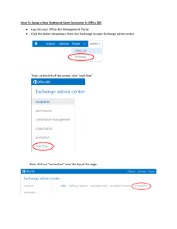


© Copyright 2026