
Here - Durham University
Durham UK-India WorkshoponMagnetisationProcesses 19th-20thMarch2015 DurhamUniversity UKIERI UK - India Education and Research Initiative Durham UK–India Workshop on Magnetisation Processes 2015 Workshop Sponsors UKIERI UK - India Education and Research Initiative This workshop is supported by the British Council through the UK-India Education and Research Initiative (UKIERI) programme, grant ref IND/CONT/E/12-13/688 ‘Nano-Engineered Magnetic Materials for Spintronic Applications’ in partnership with DST India, with additional support from Mantis Deposition Ltd., the XMaS UK CRG Beamline, and Durham University Physics Department. We are very grateful for the support provided for this meeting, which has enabled us to waive registration fees for attendees, provide refreshments, lunch, and a drinks reception, and host invited speakers. Durham UK–India Workshop on Magnetisation Processes 2015 Welcome! We warmly welcome you to the Durham UK-India Workshop on Magnetisation Processes 2015. This is a two-day workshop on thin-film and related magnetism, supported by the British Council through the UK-India Education and Research Initiative (UKIERI) programme in conjunction with the Indian department of science and technology (DST). It is funded through a collaborative research grant between the Centre for Materials Physics at Durham University and the Ultrafast Nanomagnetics group at S.N. Bose National Center for Basic Sciences, Kolkata, India. Our programme consists of invited presentations from early stage rising star researchers and academics from the UK and India. The plenary speaker is Professor Anjan Barman from SN Bose National Centre for Basic Sciences, Kolkata, India. After the first afternoon of talks there is a short panel discussion, where our Indian colleagues and visitors will describe the institutional and funding structure of research in India, followed by a reception and poster session where other attendees will present posters describing their recent research. Friday will consist of a full day of invited talks, with continuation of the poster session over lunch. We hope that you enjoy your visit to Durham and the workshop, and thank you for attending! Prof. Del Atkinson & Dr Aidan Hindmarch Cover & logo design Mustafa Tokac¸, cover image courtesy Durham University. 1 Durham UK–India Workshop on Magnetisation Processes 2015 Durham City Map Physics Department (Rochester building): #12 St. Chad’s College: #20 Durham rail station is located top center of the image above. Walking from the rail station to the Physics Department will typically take 20-25 minutes. A taxi will take 5-15 minutes, depending on traffic. 2 Durham UK–India Workshop on Magnetisation Processes 2015 Plenary Lecture Thursday Prof. Anjan Barman, S.N. Bose National Center for Basic Sciences . . . . . . . . . . . . . . . 7 Invited Talks Thursday Chair: Prof. Del Atkinson Dr Aidan Hindmarch, Durham University . . . . . . . . . . . . . . . . . . . . . . . . . . . . 11 Dr Pranaba Kishor Muduli, Indian Institute of Technology, Delhi . . . . . . . . . . . . . . . . 12 Dr Paul Keatley, University of Exeter . . . . . . . . . . . . . . . . . . . . . . . . . . . . . . . 13 Friday session 1 Chair: Prof. Brian Tanner Dr Tom Lancaster, Durham University . . . . . . . . . . . . . . . . . . . . . . . . . . . . . . 15 Dr Jaivardhan Sinha, S.N. Bose National Center for Basic Sciences . . . . . . . . . . . . . . . 16 Dr Oscar C´espedes, University of Leeds . . . . . . . . . . . . . . . . . . . . . . . . . . . . . 17 Dr Andrew Ferguson, University of Cambridge . . . . . . . . . . . . . . . . . . . . . . . . . 18 Friday session 2 Chair: Prof. Anjan Barman Dr Andrew Rushforth, University of Nottingham . . . . . . . . . . . . . . . . . . . . . . . . . 19 Dr Tom Hayward, University of Sheffield . . . . . . . . . . . . . . . . . . . . . . . . . . . . . 20 Dr Dan Read, University of Cardiff . . . . . . . . . . . . . . . . . . . . . . . . . . . . . . . . 21 Friday session 3 Chair: Prof. Peter Hatton Dr Subhankar Bedanta, National Institute of Science Education and Research . . . . . . . . . 22 Dr Will Branford, Imperial College London . . . . . . . . . . . . . . . . . . . . . . . . . . . 23 Dr Stuart Cavill, University of York . . . . . . . . . . . . . . . . . . . . . . . . . . . . . . . . 24 Dr Damien McGrouther, University of Glasgow . . . . . . . . . . . . . . . . . . . . . . . . . 25 3 Durham UK–India Workshop on Magnetisation Processes 2015 Posters From 16:15 on Thursday in the Bransden room P1: Andrew Caruana, Loughborough University . . . . . . . . . . . . . . . . . . . . . . . . . 29 P2: Sinan Azzawi, Durham University . . . . . . . . . . . . . . . . . . . . . . . . . . . . . . 30 P3: Stuart Bowe, University of Nottingham . . . . . . . . . . . . . . . . . . . . . . . . . . . . 31 P4: Oto-obong Inyang, Durham University . . . . . . . . . . . . . . . . . . . . . . . . . . . . 32 P5: Christy Kinane, STFC ISIS Neutron Facility . . . . . . . . . . . . . . . . . . . . . . . . . 33 P6: John Sinclair, University of York . . . . . . . . . . . . . . . . . . . . . . . . . . . . . . . 34 P7: Jeovani Brand˜ao, Durham University . . . . . . . . . . . . . . . . . . . . . . . . . . . . . 35 P8: Ioan Polenciuc, University of York . . . . . . . . . . . . . . . . . . . . . . . . . . . . . . 36 P9: Christopher Cox, Loughborough University . . . . . . . . . . . . . . . . . . . . . . . . . 37 P10: Mustafa Tokac¸, Durham University . . . . . . . . . . . . . . . . . . . . . . . . . . . . . 38 P11: David Burn, Imperial College London . . . . . . . . . . . . . . . . . . . . . . . . . . . 39 P12: Kowsar Shahbazi, University of Leeds . . . . . . . . . . . . . . . . . . . . . . . . . . . 40 P13: Jenny King, Durham University . . . . . . . . . . . . . . . . . . . . . . . . . . . . . . . 41 P14: Richard Rowan-Robinson, Durham University . . . . . . . . . . . . . . . . . . . . . . . 42 P15: Jaivardhan Sinha, S.N. Bose National Center for Basic Sciences . . . . . . . . . . . . . . 43 P16: Anjan Barman, S.N. Bose National Center for Basic Sciences . . . . . . . . . . . . . . . 44 4 Durham UK–India Workshop on Magnetisation Processes 2015 Plenary Lecture 5 Durham UK–India Workshop on Magnetisation Processes 2015 6 Durham UK–India Workshop on Magnetisation Processes 2015 Thursday 14:00-14:45 Investigation of Spin Dynamics Using All-Optical Techniques Anjan Barman Department of Condensed Matter Physics and Material Sciences, S. N. Bose National Centre for Basic Sciences, Block JD, Sec. III, Salt Lake, Kolkata 700 098, India [email protected] Spin waves are known for many decades while magnonics is an emerging topic with both fundamental interest and application potential. Magnons with frequencies in the GHz and sub-THz regimes have wavelengths in the nanoscale due to their smaller velocities, and magnonics fits perfectly with nanotechnology. It promises a new era of all-magnetic computation encircling on-chip information communication, processing and logic operations in addition to storage and memory. For magnonics to become a viable and sustainable technology it is essential to build a knowledge base of excitation, manipulation and detection of spin waves in various 1-D and 2-D periodic magnetic structures. Here, we present manipulation of spin waves in optically excited and detected spin dynamics in two-dimensional ferromagnetic nanodots and nanoantidots lattices. Femtosecond laser pulses are used to create hot electrons in metallic thin films and nanostructures followed by thermalization of electron and spin populations yielding a sub-picosecond demagnetization. This is followed by a two-step relaxation process and excitation of spin waves and its damping, which are detected with a sub-100 fs temporal and sub-μm spatial resolutions by a home-built time-resolved magneto-optical Kerr microscope.1 Various aspects of the dynamics as a function of the lattice constant, lattice symmetry, and bias field strength and orientation have been investigated and new observations such as magnonic mode splitting, bandgap formation, tunability of bandgaps, dynamic dephasing and transition from collective to non collective dynamics are discussed based upon the experimental data and numerical simulations.2-4 We further discuss a novel way of determining spin Hall angle in ferromagnetic/non-magnetic bilayers using time-resolved magneto-optics.5 We gratefully acknowledge financial supports from DST, Government of India and the British Council for the DST-UKIERI joint project, Grant No. DST/INT/UK/P-44/2012. We also acknowledge financial support from DST under Grant No. SR/NM/NS-09/2011(G). 1. A. Barman and A. Haldar, Solid State Physics 65, 1-108 (2014). 2. B. Rana et al., ACS Nano, 5, 9559 (2011). 3. R. Mandal et al., ACS Nano 6, 3397 (2012). 4. S. Saha et al., Advanced Functional Materials 23, 2378 (2013). 5. A. Ganguly et al., Appl. Phys. Lett. 105, 112409 (2014). 7 Durham UK–India Workshop on Magnetisation Processes 2015 8 Durham UK–India Workshop on Magnetisation Processes 2015 Invited Talks 9 Durham UK–India Workshop on Magnetisation Processes 2015 10 Durham UK–India Workshop on Magnetisation Processes 2015 Thursday 13:30-14:00 Crystal phase and interface dependent spin-mixing conductance in polycrystalline cobalt thin-films A.T. Hindmarch*1, M. Tokac1, S.A. Bunyaev2, G. N. Kakazei2, D.S. Schmool3, D. Atkinson1 (1) Centre for Materials Physics, Durham University, Durham, UK (2) IFIMUP and IN, Departamento de Fisica e Astronomia, Universidade do Porto, Portugal (3) Laboratorie PROMES CNRS UPR 8521 University of Perpignan Via Domitia, France *Email: [email protected] A quantitative physical analysis of spin-currents traversing interfaces in ferromagnetic thin-film multilayers will provide a deeper fundamental understanding applications of such nanoscale magnetic systems in spintronics, magnonics, and spin-caloritronics. Precessional magnetization dynamics have been used extensively to access interfacial spin transport where spin-current flows from precession in a ferromagnetic thin-film, into an adjacent non-magnetic layer where it is dissipated under the influence of the spin-orbit interaction resulting in an enhanced damping in the ferromagnetic layer – a process known as spin-pumping. In this talk I will describe growth of multi-layered thin films where we are able to control the dominant crystal phase in a ferromagnetic cobalt film as a function of thickness; we induce a nonequilibrium fcc (111) texture through growth on suitable seed layers, and allow relaxation to a bulklike hcp (0001) phase with increasing film thickness. I will then outline some recent results from our research group where we have been investigating transmission of pure spin-currents via ‘spinpumping’ under ferromagnetic resonance. Using measurements on sets of device structures with different overlayers we show that the nature of the atomic scale structure in the vicinity of the interface plays a dominant role in the transmission of pure-spin currents, creating significant differences in the enhancement of precessional magnetisation damping. 11 Thursday 15:00-15:30 Durham UK–India Workshop on Magnetisation Processes 2015 Recent advances in magnetic tunnel junction based spin torque nanooscillators Pranaba Kishor Muduli* Department of Physics, Indian Institute of Technology, Hauz Khas, New Delhi-110016, India *Email: [email protected] Spin transfer torque (STT) allows manipulation of magnetic moments in nano-sized magneto-resistive devices using current instead of magnetic field.1, 2 In certain sample geometries and/or applied fields, STT can maintain a steady precession of one or more magnetic moments.3 As a consequence, the device resistance undergoes oscillation, either through giant magnetoresistance (GMR) or tunneling magnetoresistance (TMR), producing an output voltage signal in the microwave frequency range. These so-called Spin Torque Nano Oscillators (STNOs) are typically based either on nanocontacts on top of GMR stacks, or nanopillars of GMR or TMR stacks. In this talk, I will first discuss nanocontacts devices based on metallic spin-valves and show the experimental confirmation of spin torque induced propagating spin waves,4 formation of magnetic droplet5 and synchronization of three nanocontact STOs fabricated close to each other.6 I will then present our recent results on frequency noise measurements7 for understanding coherence mechanisms in a magnetic tunnel junction (MTJ) based STNO and show how mode-hopping mechanism generates a 1/f frequency noise. I will discuss how to reduce linewidth and enhance power of the STNOs for practical applications by demonstrating parametric excitation and synchronization.8 Finally I will show our first results on wireless communication of MTJ based STNOs up to a distance of 150 m with a data rate of ~3 Mbps. Acknowledgement: Partial support by DST Fast-Track Project is gratefully acknowledged. Support from the Swedish Foundation for Strategic Research (SSF) and the Swedish Research Council (VR) are gratefully acknowledged. References: 1. 2. 3. 4. 5. 6. 7. 8. 12 J. Slonczewski, J. Magn. Magn. Mater. 159, L1-L7 (1996). L. Berger, Phys. Rev. B 54, 9353-9358 (1996). S. I. Kiselev, J. C. Sankey, I. N. Krivorotov, N. C. Emley, R. J. Schoelkopf, R. A. Buhrman and D. C. Ralph, Nature 425 (6956), 380-383 (2003). S. Bonetti, V. S. Tiberkevich, G. Consolo, G. Finocchio, P. Muduli, F. Mancoff, A. N. Slavin and J. Åkerman, Phys. Rev. Lett. 105 (21), 217204 (2010). S. M. Mohseni, S. R. Sani, J. Persson, T. N. A. Nguyen, S. Chung, Y. Pogoryelov, P. K. Muduli, E. Iacocca, A. Eklund, R. K. Dumas, S. Bonetti, A. Deac, M. A. Hoefer and J. Akerman, Science 339 (6125), 1295-1298 (2013). S. Sani, J. Persson, S. M. Mohseni, Y. Pogoryelov, P. K. Muduli, A. Eklund, G. Malm, M. Kall, A. Dmitriev and J. Akerman, Nat. Commun. 4, 2731 (2013). R. Sharma, P. Durrenfeld, E. Iacocca, O. G. Heinonen, J. Akerman and P. K. Muduli, Appl. Phys. Lett. 105 (13), 132404 (2014). P. Durrenfeld, E. Iacocca, J. Akerman and P. K. Muduli, Appl. Phys. Lett. 104 (5), 052410 (2014). Durham UK–India Workshop on Magnetisation Processes 2015 Thursday 15:30-16:00 Time-resolved scanning Kerr microscopy of magnetization dynamics at the nanoscale P.S. Keatley*1 and R.J. Hicken1 (1) School of Physics and Astronomy, University of Exeter, Exeter UK *Email: [email protected] Time-resolved scanning Kerr microscopy (TRSKM) is a powerful tool for the investigation of the magnetization dynamics at sub-micrometer length scales with picosecond temporal resolution.[1,2] A variety of measurement configurations allows a range of dynamic magnetic phenomena to be explored including sub-gigahertz gyrotropic oscillations of magnetic vortices, picosecond magnetic reorientation in hard disk writers, domain wall dynamics and excitations in nanowires, non-uniform confinement of spin waves in nanomagnets, and low-temperature ferromagnetic resonance of thin films. Recently TRSKM has been used to understand the coupled response of vortices, domain walls, and spin-waves that govern the behaviour of magnonic metamaterials for magnetic logic and signal processing applications. At the same time, the influence of a spin-torque on these magnetic excitations is of fundamental interest for spintronic devices for non-volatile memory elements and microwave oscillators. In this presentation the results of TRSKM on individual nanomagnets are presented, Figure 1. The influence of the precise shape, material parameters, and a spin-torque on the confined spin waves modes of an individual nanomagnet will be discussed in addition to the effect of nearest neighbour static and dynamic dipole interactions in pairs of nanomagnets. Finally, a summary of recent developments in TRSKM for the detection of magnetisation dynamics in active spintronic devices and for the prospect of sub-diffraction spatial resolution will be presented. (a) fK 300 nm hRF (t) Frequency Frequency (GHz) (GHz) 10 H 8 -f K 6 10 (b) 4 8 2 6 +f K (c) 4 2 -1.0 -0.5 0.0 -M z 0.5 1.0 0.5 +M z 0.0 -0.5 -1.0 Magnetic field (kOe) Figure 1. (a) TRSKM measurements with coherent microwave field excitation on a pair of NiFe(15 nm) discs with 300 nm diameter and edge-to-edge separation of 160 nm (inset). (b) Spinwave spectrum acquired from one of the discs showing respectively the higher and lower frequency branches of the centre and edge modes, in agreement with micromagnetic simulations (c). [1] P.S. Keatley, V.V. Kruglyak, P. Gangmei, and R.J. Hicken, Philosophical Transactions of the Royal Society A: Mathematical, Physical and Engineering Sciences, 369, 3115 (2011). [2] P.S. Keatley, P. Gangmei, M. Dvornik, R.J. Hicken, J. Grollier, C. Ulysse, J.R. Childress, and J.A. Katine, Topics in Applied Physics, 125, 17 (2013). 13 Durham UK–India Workshop on Magnetisation Processes 2015 14 Durham UK–India Workshop on Magnetisation Processes 2015 Friday 09:15-09:45 Using implanted muons to investigate order, disorder and excitations in reduced dimensions Tom Lancaster*1 (1) Department of Physics, Durham University, Durham DH1 3LE *Email: [email protected] Implanted muons are a sensitive means of investigating magnetic order, disorder and dynamics and the properties of magnetic textures. I will review the use of the technique in investigations of lowdimensional magnetic systems, concentrating on the case of molecular coordination polymers, which are materials that can show two-, one- or even zero-dimensional behaviour. In favourable cases we have been able to control the dimensionality of a system through chemical or physical means. I will also describe the use of muons in investigating the skyrmion lattice, by exploiting the analogy between skyrmion and vortex lattice physics. 15 Friday 09:45-10:15 Durham UK–India Workshop on Magnetisation Processes 2015 Perpendicular Magnetic Anisotropy and Magnetic Inhomogeneity in Ta(N)/CoFeB/MgO J. Sinha1, C. Banerjee1, A. K. Chaurasiya1, A. Ganguly1, M. Hayashi2 and A. Barman1 (1) Thematic Unit of Excellence on Nanodevice Technology, Department of Condensed Matter Physics and Material Sciences, S. N. Bose National Centre for Basic Sciences, Salt Lake, Kolkata 700 098, India (2) National Institute for Materials Science, Tsukuba 305-0047, Japan Email: [email protected] In-depth understanding of perpendicular magnetic anisotropy (PMA) in thin film with structure inversion asymmetry is important to develop advanced spintronics devices [1]. The thin film heterostructure CoFeB|MgO with Heavy Metal (HM- Ta, TaN) underlayer has drawn much attention recently as it posses sufficient interface anisotropy to exhibit PMA [1,2]. Specially, Ta|CoFeB|MgO is the main constituent of magnetic tunnel junction [1] and it has significant application potential in recently discovered three terminal devices [3]. Though in this heterostructure interface anisotropy primarily originates from CoFeB|MgO interface but the choice of underlayer significantly influences the strength of PMA. It has been found recently that the interface anisotropy in Ta|CoFeB|MgO film can be varied by changing the N-flow rate during Ta underlayer deposition [2]. Specifically CoFeB|MgO films grown on optimally N-doped Ta underlayer has larger interface anisotropy than the film deposited on Ta underlayer. In order to assess the technological potential of these heterostructures it is important to understand the magnetic inhomogeneity which is an important contributor to the damping coefficient. A powerful method to study the magnetic inhomogeneity is to investigate the spin-wave linewidth. Brillouin Light Scattering (BLS) is a sensitive probe for detecting spin-waves in magnetic thin films and multilayers [4,5,6]. The detailed magnetic properties (saturation magnetization, magnetic dead layer thickness, and interface anisotropy) in Ta(N)|CoFeB|MgO will be discussed. It will be further shown that the magnetic inhomogeneity can be tuned in these heterostructures by doping N into the underlayer. Acknowledgement: We acknowledge the financial assistance from Department of Science and Technology Govt. of India under grant no. SR/NM/NS-09/2011 and S. N. Bose National Centre for Basic Sciences under project no. SNB/AB/12-13/96. Reference: [1] S. Ikeda et al., Nature Materials 9, 721 (2010). [2] J. Sinha et al., Appl. Phys. Lett. 102, 242505 (2013). [3] L. Liu et al., Science 336, 555 (2012). [4] B. Hillebrands, Phys. Rev. B, 41, 530 (1990). [5] A. Haldar et al., J. Appl. Phys. 115, 133901 (2014). [6] G. Gubbiotti et al., Phys. Rev. B, 86, 014401 (2012). 16 Friday 10:15-10:45 Durham UK–India Workshop on Magnetisation Processes 2015 Spin Physics in Hybrid Metallo-Molecular Multilayers O. Cespedes*1, M. Wheeler1, T. Moorsom1, F. Al Ma’Mari1, G. Burnell1, B.J. Hickey1, G. Teobaldi2, F. Gonzalvez3, R. Stamps3 (1) School of Physics & Astronomy, University of Leeds, LS2 9JT, UK (2) Department of Chemistry, University of Liverpool, L69 3BX, UK (3) School of Physics & Astronomy, Kelvin Building, University Avenue, Glasgow, G12 8QQ, UK *Email: [email protected] Carbon based materials are attractive for spintronic applications due to their long spin coherence time and the possibility to implement low-dissipation electronics in eco-friendly devices. In the past, this research has been mostly focused on reproducing the magnetoresistance (MR) of standard spin valves and magnetic tunnel junctions but using organic spacers. These devices have proven successful, with MR of up to 5-10% in spacers up to ~100 nm thick.1 The role of the interface and the generation of proximity effects at the molecular material have been discussed extensively; orbital shifting and hybridisation play an essential role when discussing the spin-dependent transmission probability, and copper-molecular bilayers have been demonstrated to give rise to spin filtering.2 0 SiO2 1.4 1.5 1.6 1.7 Emission (eV) 1.8 Al 2 O 3 Magnetic Al 2 O 3 10 Non-magnetic Spin Polarised Effect in NPL 20 Al2O3 PY Al 2 O 3 Non-magnetic PY current with / no MF Magnetic Al2O3 PY current PY current (MF) 0.8 Au current 30 0.9 Au current (MF) Intensity (counts/s) Au Al2O3 40 Negative luminescence (NPL) Au / no current no MF 1.0 0 current V I Au / no current with MF 1.1 0 current (MF) 50 Normalized emission More recently, the research has shifted towards the possibility of using spin pumping into organic materials.3 This method of spin injection would eliminate the problem of resistivity mismatch and opens the doors for the propagation of pure spin currents without an applied voltage in low spin orbit materials. Here, we will first show the effect of charge transfer in metallo-molecular multilayers, demonstrating the appearance of an antiferromagnetic coupling4 and changes in the spectroscopic properties of the molecules.5 We will then consider the effects of energy dissipation from a ferromagnet into a fullerene film during ferromagnetic resonance. Figure 1: Schematic of a device used to study the effects of spin polarization in photoluminescence and changes measured as a function of the direction of the current and the applied magnetic field. [1] X. Zhang et al., Nature Communications, 4, 2423 (2013). [2] K.V. Raman et al., Nature, 493, 509 (2013) [3] K. Ando et al., Nature Materials, 12, 633 (2013). [4] T. Moorsom et al., Phys. Rev. B , 90, 125311 (2014). [5] T. Moorsom et al., Appl. Phys. Lett., 105, 022408 (2014) 17 Friday 10:45-11:15 Durham UK–India Workshop on Magnetisation Processes 2015 Spin-orbit torques in ferromagnets with broken inversion symmetry Andrew Ferguson* Cavendish Laboratory, JJ Thomson Avenue, Cambridge, CB3 0HE *Email: [email protected] Passing electricity through a ferromagnetic conductor with uniform magnetisation and with broken inversion symmetry may generate a torque [1]. This so-called spin-orbit torque can be used to switch the magnetisation in ferromagnetic semiconductors at low temperature [2] and also in ferromagnetic metals at room temperature [3], as might be useful in a memory device. Here I will summarise the work of my group and collaborators on spin-orbit torque, using (Ga,Mn)As as a model system. By employing current driven ferromagnetic resonance we are able to map out the magnitude and direction of the field like spin-orbit torques [4]; observe an intrinsic anti-damping spin-orbit torque originating in the Berry phase [5]; and measure the reciprocal effect to the spin-orbit torque [6], whereby the precessing magnetisation pumps a charge current. [1] [2] [3] [4] [5] [6] 18 B. A. Bernevig and O. Vafek, Phys Rev B 72, 187601 (2005); A. Manchon and S. Zhang, Phys Rev B 78, 187601 (2008); A. Manchon and S. Zhang, Phys Rev B 79, 187601 (2009). A. Chernyshov, M. Overby, X. Y. Liu, J. K. Furdyna, Y. Lyanda-Geller, and L. P. Rokhinson, Nat Phys 5, 656 (2009). I. M. Miron, K. Garello, G. Gaudin, P. J. Zermatten, M. V. Costache, S. Auffret, S. Bandiera, B. Rodmacq, A. Schuhl, and P. Gambardella, Nature 476, 189 (2011). D. Fang, H. Kurebayashi, J. Wunderlich, K. Vyborny, L. P. Zarbo, R. P. Campion, A. Casiraghi, B. L. Gallagher, T. Jungwirth, and A. J. Ferguson, Nat Nanotechnol 6, 413 (2011). H. Kurebayashi, J. Sinova, D. Fang, A. C. Irvine, J. Wunderlich, V. Novak, R. P. Campion, B. L. Gallagher, E. K. Vehstedt, L. P. Zarbo, K. Vyborny, A. J. Ferguson, and T. Jungwirth, Nat Nanotechnol 9, 211 (2014). C. Ciccarelli, K. M. D. Hals, A. Irvine, V. Novak, Y. Tserkovnyak, H. Kurebayashi, A. Brataas, and A. Ferguson, Nat Nanotechnol 10, 50 (2015). Durham UK–India Workshop on Magnetisation Processes 2015 Friday 11:30-12:00 Magnetic Domain Walls Under Strain Andrew Rushforth*1 (1) School of Physics and Astronomy, University of Nottingham, Nottingham NG7 2RD, UK. *Email: [email protected] Magnetic domain walls are the important constituents of many existing and proposed technologies. These technologies include information storage devices, such as 3-terminal magnetic random access memory (DW-MRAM)[1] and racetrack memory[2], information processing concepts using the position[3] and chirality[4] of domain walls to represent the bit of information, and more diverse applications such as in lab-on-a-chip[5] devices and motion sensors[6]. Traditional methods to control the motion of magnetic domain walls rely on external magnetic fields or electrical currents. These methods place limits on the energy efficiency and miniaturisation of devices. A promising alternative route to low energy control of magnetisation is to use electric fields. In particular, the application of voltage-induced mechanical strain in hybrid piezoelectric/ferromagnetic devices has received much attention recently[7,8]. The mechanical strain induces a magnetic anisotropy in the ferromagnetic layer via inverse magnetostriction. This approach has been used to demonstrate non-volatile switching of the magnetisation direction[9], control of the efficiency of current induced domain wall motion[10,11], and predictions that domain wall structure[12] and position[13] can be controlled by voltage induced strain alone. In this talk I will review our recent work to study magnetic domain walls under the action of voltageinduced strain. Collaborative projects between researchers at the Universities of Nottingham, Cambridge, Leeds, Sheffield, York, and at Diamond Light Source have investigated domain walls in devices from macroscopic to sub-micrometre length scales, and under the action of magnetic fields, electrical currents, and in nanostructured devices with intentionally designed pinning sites. In all of these regimes, the action of mechanical strain is found to significantly modify the properties and dynamics of domain walls. [1] Fukami, S. et al., 2009 Symposium on VLSI Technology Digest of Technical Papers, 230–1 (2009). [2] Parkin, Patent US 6834005; Science 320, 190 (2008). [3] D.A. Allwood et al., Science 309, 1688 (2005). [4] Omari, et al., Phys. Rev. Appl. 2, 044001 (2014). [5] Rapoport et al., Lab Chip, 12, 4433–4440 (2012). [6] Novotechnik, http://www.novotechnik.com/rsm [7] Hu et al., Nature. Communications. 2, 553 (2011). [8] Biswas et al., Sci. Rep. 4, 7553 (2014). [9] Parkes et al., Appl. Phys. Lett 101, 072402 (2012). [10] De Ranieri et al., Nature Materials 12, 808 (2013). [11] Rushforth, App. Phys. Lett. 104, 162408 (2014). [12] Bryan et al., J. Phys.: Condens. Matter 24, 024205 (2012). [13] Dean et al., J. Appl. Phys. 109, 023915 (2011). 19 Friday 12:00-12:30 Durham UK–India Workshop on Magnetisation Processes 2015 Understanding and Controlling Stochastic Domain Wall Behaviour in Magnetic Nanowire Devices T.J. Hayward1, K. Omari1, M. Negiotia1, T.J. Broomhall1, M.P.P. Hodges1, P.W. Fry2, D.A. Allwood1, M.T. Bryan3, M.-Y. Im4 and P. Fischer4 1 Department of Materials Science and Engineering, University of Sheffield, UK. 2 Nanoscience and Technology Centre, University of Sheffield, UK 3 Department of Cardiovascular Science, University of Sheffield, UK 4 Centre for X-ray Optics, Berkeley National Laboratory, Berkeley, CA, USA Devices based on the controlled motion of domain walls (DWs) in planar magnetic nanowires have great technological potential. However, the realisation of such technologies has long been hindered by a number of fundamental problems. Some of the most serious of these relate to stochastic DW pinning/depinning effects. For example, in nominally defect-free nanowires, DW transmission is found to be probabilistic even for fields much greater than those required to initiate DW propagation [1]. Furthermore, in nanowires containing artificial defect sites, different fields/currents are required to depin DWs from one instance to the next, and DWs may pass dynamically through the defects under applied fields that are not expected to cause depinning [2]. Here, we will use finite temperature micromagentic simulations to show that all of these experimentally observed behaviours can be comprehensively explained by a complex, dynamical interaction between thermal perturbations and Walker breakdown phenomena. Our results show that stochastic phenomena are an intrinsic feature of DW behaviour at finite temperatures, and would not be suppressed even in hypothetical systems where initial DW structures and external parameters were perfectly defined. Having explored the origins of stochastic DW pinning we will discuss a number of potential solutions. These range from simple solutions, such as tuning defect sites and/or nanowire geometries in order to simplify their interaction with dynamically propagating DWs, to more complex approaches where DWs are carried directly by propagating 1D potential wells, created by either rotating magnetic fields or by the interference of surface acoustic waves. Finally we will use micromagnetic simulations to illustrate a potential material science-based solution, where doping Ni80Fe20 nanowires with rareearth elements creates systems where the complex magnetisation dynamics at the heart of stochastic phenomena are almost entirely suppressed. [1] M. Muñoz and J. Prieto, Nature Communications 2, 526 (2011), H. Tanigawa, T. Koyama, M. Bartkowaik, S. Kasai, K. Kobayashi and T. Ono, Phys. Rev. Lett 101, 207203 (2008). [2] U.-H. Pi, Y.-J. Cho, J.-Y. Bae, S.-C. Lee and S. Seo, Phys. Rev. B. 84, 024426 (2011), M.-Y. Im, L. Bocklage, P. Fischer and G. Meier. Phys. Rev. Lett. 102, 147204 (2009). Figure 1: Results of room-temperature micromagnetic simulations in which vortex domain walls with anticlockwise circulations were propagated to a notchshaped defect site at H = 35 Oe. The upper figure illustrates the multitude of pinned domain wall configurations formed at the notch. The lower plot indicates the frequency of their formation and a derived depinning field distribution. 20 Durham UK–India Workshop on Magnetisation Processes 2015 Friday 12:30-13:00 Imaging Magnetic Domains in Nano-Structured Thin Films for Data Storage Applications Dan Read1* School of Physics & Astronomy, Cardiff University, Queen’s Buildings, The Parade, Cardiff, CF24 3AA, UK 1 * e-mail: [email protected] In the current race for information storage media with ever increasing data densities the position or state of magnetic domain walls, the region in a magnetic system where the local magnetization continually rotates its direction between adjacent magnetic domains, is one of the most promising routes for future storage media and devices. Information storage requires ultrafast read-out and writing operations, but domain walls need to be pinned so that the information is safely stored in the long term. Here we investigate the use of a variety of pinning schemes and geometries to assess those that might be best for future device technologies. One promising candidate is to utilise remote magnetostatic charges to trap magnetic domain walls [1]. Over the years a great variety of imaging techniques such as, Magnetic Force Microscopy (MFM) Scanning Magneto-Optic Kerr Effect Microscopy (MOKE) or Lorentz Electron Microscopy have been used to image domain walls [2,3]. By using Scanning Transmission X-ray Microscopy (STXM) and X-ray photoelectron emission microscopy (XPEEM) we have followed the position and structure of domain walls of opposite charge being pinned or repelled by pinning potentials of increasing strength. Micromagnetic simulations have been performed and have shown excellent agreement with the experimental results. We demonstrate the attractive or repulsive character of the interaction between domain wall and trap depending upon the sign of their magnetic charges. These quasi-static experiments are the antecedent to ultrafast time-resolved XMCD-PEEM experiments where the spin-transfer torque effect will be studied dynamically by applying picosecond-long current pulses across the magnetic nanowire. [1] O’Brien et al., “Tunable Remote Pinning of Domain Walls in Magnetic Nanowires”, Physical Review Letters, 106 087204, (2011). [2] Ladak et al., “Direct observation of magnetic monopole defects in an artificial spin-ice system”, Nature Physics, 6 359, (2010). [3] Petit et al., “Magnetic imaging of the pinning mechanism of asymmetric transverse domain walls in ferromagnetic nanowires”, Applied Physics Letters, 97 233102, (2010). 21 Friday 14:00-14:30 Durham UK–India Workshop on Magnetisation Processes 2015 Magnetization reversal study by magneto-optic Kerr microscopy Subhankar Bedanta National Institute of Science Education and Research (NISER), Institute of Physics Campus, Po- Sainik School, Bhubaneswar, Odisha, India-751005 *[email protected] Magneto-optic Kerr effect (MOKE) magnetometry has been widely performed to study and measure magnetic hysteresis in ferromagnetic thin films. This technique is often preferred because it is cost effective, fast measurement time and more importantly the capability of performing the vector magnetometry. There are three configurations of MOKE magnetometry exists such as longitudinal, transverse and polar, respectively. In past few decades Kerr microscopy based on the MOKE principle has been often performed to image ferromagnetic domains. In this talk I will give a brief overview of Kerr magnetometry and microscopy. In particular I will highlight the significance of these techniques in studying magnetization reversal processes. In this context I will show our recent results on four subjects which are listed below. (i) Superferromagnetism (SFM): SFM domains in a non-percolated nanoparticle assembly are expected to be similar to conventional ferromagnetic domains in a continuous film, with the decisive difference that the atomic spins are replaced by the superspins of the single-domain nanoparticles. [1,2] From the domain wall relaxation measurements we can calculate the domain wall velocity and plot it as a function of external magnetic fields. The various domain wall dynamic modes such as creep, slide and the depinning transition have been clearly observed. Angle dependent magnetization reversal study has been performed which indicate that the size and relaxation dynamics can be controlled by changing the angle between the easy axis and the magnetic field. [3] (ii) Magnetic antidot arrays (MALs): MALs are defects in a continuous thin film. They introduce perturbation in the thin film and hence their magnetization reversal mechanism is quite different from that of a continuous thin film. MALs are receiving intense research interest because of their potential advantages, such as lack of superparamagnetic limit to the bit size (as compared to dot arrays) [4]. We will show how the magnetization reversal process occurs in a Co MAL system studied by Kerr microscopy. [5] (iii) Inter-layer coupling: The other topic of interest is competing inter-layer interaction effects in dipolarly coupled ferromagnetic/non-magnetic multilayers. LMOKE microscopy has been performed on [Co (t1)/Al2O3(t2)]N for various thicknesses of Co (t1) and Al2O3 (t2) and different number of bilayers, respectively. We will show how the inter-layer interactions lead to layer-by-layer magnetization reversal as evidenced by Kerr microscopy. [6-8] iv) Interplay of uniaxial and cubic anisotropies in Fe/MgO(100) epitaxial thin film: I will present a study on magnetization reversal process for Fe/MgO(001) thin films. Due to the oblique growth configuration, a uniaxial anisotropy is found superimposed to the expected four-fold cubic anisotropy. Domain wall motion images during magnetization reversal are captured by Kerr microscope which are the clear evidence of two successive or separate 90° DW nucleation depending on the angle between the applied field and easy axis i.e. <100> direction. Still now all systematic studies on magnetization reversal mechanism of epitaxial Fe/MgO(001) film were explained on the basis of theoretical models. But for the first time we are presenting the direct evidences of magnetization reversal mechanism in this system. [9] References: [1] S. Bedanta and W. Kleemann, J. Phys. D : Appl. Phys. 42, 013001 (2009) [2] S. Bedanta et al. Phys. Rev. Lett. 89, 176601 (2007); [3] N. Chowdhury et al. J. Appl. Phys. (under review); [4] N. G. Deshpande et al, JAP 111, 013906 (2012); [5] Sougata Mallick and S. Bedanta, J. Magn. Magn. Mater. 352, 158 (2015); [6] S. Bedanta et al. Phys. Rev. B 74, 054426 (2006) ; [7] N. Chowdhury and S. Bedanta, AIP Advances 4, 027104 (2014) ; [8] N. Chowdhury and S. Bedanta et al. (unpublished) ; [9] Srijani Mallick, N. Chowdhury and S. Bedanta, AIP Advances 4, 097118 (2014) 22 Durham UK–India Workshop on Magnetisation Processes 2015 Friday 14:30-15:00 Collective Properties of Nanomagnet Arrays; Electric and Magnetic Currents in Artificial Spin Ice W. Branford*1, (1) Blackett Laboratory, Dept of Physics, Imperial College London, SW72AZ *Email: [email protected] I will discuss large-area arrays of single domain nanomagnets with frustrated interactions. The shape of each nanomagnet controls the magnetic anisotropy and the elements are closely spaced so dipolar interactions are important. Lattices are chosen such that the geometry prevents all dipole interactions from being satisfied. Arrays of this type are generally called Artificial Spin Ice and I will describe experiments on electrically continuous permalloy honeycombs structures. [1-2] Here I report direct magnetic imaging studies of domain wall mediated magnetic charge flow in artificial spin ice. [3-5]. The magnetic charge is carried by transverse domain walls and the chirality of the domain wall is found to control the direction of propagation. Recently it has been shown that in isolated Y-shaped junctions that support vortex domain walls, selectivity can be determined by chirality (or topology), the suggestion being that vortex wall chirality is robust in the Walker breakdown process.[6,7] Here I will show that in Y-shaped junctions, magnetic switching in the important topologically protected regime exists only for a narrow window of field and bar geometry, and that it will be challenging to access this regime in field-driven Artificial Spin Ice. This work has implications for the wider field of magnetic charge manipulation for high density memory storage. [1] S. Ladak, D. E. Read, G. K. Perkins, L. F. Cohen & W. R. Branford. Nature Physics 6, 359, (2010). [2] W. R. Branford, S. Ladak, D. E. Read, K. Zeissler & L. F. Cohen. Science 335, 1597, (2012). [3] S. K. Walton, K. Zeissler, D. M. Burn, S. Ladak, D. E. Read, T. Tyliszczak, Cohen, L. F. & Branford, W. R. New Journal of Physics 17, 013054, (2015). [4] K. Zeissler, S. K. Walton, S. Ladak, D. E. Read et al. Sci. Rep. 3, 01252, (2013). [5] S. Ladak, D. Read, T. Tyliszczak, W. R. Branford & L. F. Cohen. New Journal of Physics 13, 023023, (2011). [6] T. Phung, A. Pushp, C. Rettner, B. P. Hughes, S. H. Yang & S. S. P. Parkin. Appl. Phys. Lett. 105, 222404, (2014). [7] A. Pushp, T. Phung, C. Rettner, B. P. Hughes, S. H. Yang, L. Thomas & S. S. P. Parkin. Nature Physics 9, 505-511, (2013). 23 Friday 15:00-15:30 Durham UK–India Workshop on Magnetisation Processes 2015 Strain Induced Vortex Core Switching in Planar Magnetostrictive Nanostructures T. A. Ostler1, R. Cuadrado1, R. W. Chantrell1, A. W. Rushforth2 and S. A. Cavill1,3* 1 2 Department of Physics, University of York, Heslington, York, YO10 5DD, United Kingdom School of Physics and Astronomy, The University of Nottingham, Nottingham, NG7 2RD, United Kingdom 3 Diamond Light Source, Chilton, Didcot, Oxfordshire, OX11 0DE, United Kingdom Magnetic vortex cores, often found in planar magnetic structures, arise from the complex interactions between the magnetostatic and exchange energy. In recent years the magnetization dynamics of the core have also been studied in great detail because the gyrotropic mode has applications in spin torque driven magnetic microwave oscillators, and also provides a means to flip the direction of the core for use in magnetic storage devices such as magnetic random access memory. The excitation of the core gyrotropic mode can be achieved using various stimuli such as RF or pulsed magnetic fields or spinpolarized currents. Here we demonstrate a new means of stimulating magnetization reversal of the vortex core by applying a time-varying strain to planar structures of the magnetostrictive material, Fe81Ga19 (Galfenol), coupled to an underlying piezoelectric layer. Using micromagnetic simulations we have shown that the vortex core state can be deterministically reversed by electric field control of the time-dependent strain-induced anisotropy. These theoretical results can be used as a recipe for designing experimental setups and could pave the way for low energy devices based on the magnetic vortex core. 24 Durham UK–India Workshop on Magnetisation Processes 2015 Friday 15:30-16:00 Nanometer resolution imaging of Helical and Skyrmion states in FeGe D. McGrouther*1, S. McVitie1, R. L. Stamps1, T. Koyama2, Y. Nishimori2, Y. Togawa2 (1) University of Glasgow, Glasgow, G12 8QQ, United Kingdom (2) Osaka Prefecture University, Osaka, Japan *Email: [email protected] The behaviour of materials with B20 crystal structure is the focus of current attention due to a desire to understand the varied and complex behaviour arising from the chiral Dzyaloshinskii-Moriya interaction. In a phase diagram, depending on both temperature and magnetic field strength, ordered helical and Skyrmion states have been observed and widely reported. Materials such as FeCoSi[1], MnSi[2] and Cu2OSeO3[3] have received much attention but these exhibit magnetic ordering at temperatures well below 100K. FeGe exhibits a much higher magnetic ordering temperature, in the region 250-280K[4] and thus holds more potential for future application. At Glasgow we have developed world-leading high spatial resolution imaging (resolution better than 1 nm) for magnetic materials. On an aberration corrected JEOL ARM200FCS Scanning Transmission Electron Microscope (STEM) we have utilised the Differential Phase Contrast (DPC) mode to study the magnetic behaviour of a <100nm thick, (110) oriented sheet of FeGe cut from a bulk crystal. Using a specimen cooling holder we have imaged magnetic behaviour in various regimes of the phase diagram, from 110-250K and by applying magnetic fields of strength 0-3kOe. Our quantitative imaging capabilities, coupled with an applied spatial resolution of 3 nm for these samples, have allowed us to investigate in detail the transition from helical to Skyrmion phase, the evolution of the Skyrmion structure under applied fields and interesting behaviours that arise at phase boundaries. Figure 1. The Skyrmion lattice, period 74 nm, occurring at 250K stabilised by an applied field of strength 400 Oe. [1] X. Z. Yu, et al., Nature 465, 09124 (2010) [2] E. Karhu, et al., Physical Review B, 82, 184417 (2010) [3] S. Seki, et al., Science 336, 198 (2012) [4] X. Z. Yu, et al., Nature Materials 10, 106 (2011) 25 Durham UK–India Workshop on Magnetisation Processes 2015 26 Durham UK–India Workshop on Magnetisation Processes 2015 Thursday 19th, from 16:15 Posters 27 Durham UK–India Workshop on Magnetisation Processes 2015 28 Durham UK–India Workshop on Magnetisation Processes 2015 Poster P1 Feasibility of Spin Seebeck Based Thermoelectrics A.J. Caruana*1, K. Morrison1 (1) Physics Department, Loughborough University, Loughborough, UK. *Email: [email protected] Thermoelectric generators (TEGs) are of increasing interest due to their potential use in energy harvesting of waste heat. The efficiency of such devices is often characterised by the thermoelectric figure of merit, zT[1], which is ultimately limited by the thermal and electric conductivities in conventional TEGs. The ideal TEG material should have a high electrical conductivity (to reduce resistive losses), and low thermal conductivity (so that a large temperature gradient can be setup across the device) for the optimisation of zT. However, these properties are intrinsically linked to one another, as best described by the Weidemann-Franz Law (κ=σL0T), thus providing a limit to the upper value of zT. The Spin Seebeck Effect (SSE) may provide a way in which to overcome this limit. Rather than the generation of a charge current, Jc, in response to a thermal gradient, a spin polarized current, Js, arises when a thermal gradient is applied to a magnetised layer. If a paramagnetic metallic contact is deposited on top of the magnetic layer, this spin polarized current can be detected/harvested via the inverse spin hall effect (ISHE) (see Figure 1)[2]. Due to the separation of the active material (magnetic layer) and the electric circuit (paramagnetic layer) the magnetic layer can be chosen so that the thermal conductivity is minimised without affecting the electrical conductivity of the contact layer (and thus maximising device efficiency). We will present a broad overview of the current state of the art with regards to thermoelectric materials, followed by a discussion of the merits of integrating the spin Seebeck effect in TEGs. [1] L. E. Bell, Science, 321, 1457 (2008) [2] K. Uchida et al, J. Phys. Condens. Matter, 26, 343202 (2014) Figure 1: Schematic diagram of the two Spin Seebeck effect configurations. In both cases the bottom magnetic layer is magnetised as a thermal gradient is applied along (transverse), or through (longitudinal) the device. This causes a spin accumulation in the device, which induces a charge voltage in the top contact layer. 29 Poster P2 Durham UK–India Workshop on Magnetisation Processes 2015 Understanding the thickness dependence of Gilbert damping in ferromagnetic thin films with non-magnetic capping layers 𝐒. 𝐀𝐳𝐳𝐚𝐰𝐢∗𝟏 , 𝐀. 𝐆𝐚𝐧𝐠𝐮𝐥𝐲 𝟐 , 𝐉. 𝐀. 𝐊𝐢𝐧𝐠 𝟏, 𝐉. 𝐒𝐢𝐧𝐡𝐚𝟐, 𝐀. 𝐓. 𝐇𝐢𝐧𝐝𝐦𝐚𝐫𝐜𝐡 𝟏 𝐀. 𝐁𝐚𝐫𝐦𝐚𝐧 𝐃. 𝐀𝐭𝐤𝐢𝐧𝐬𝐨𝐧 𝟏 1 Durham University 2 S. N. Bose National Centre for Basic Sciences 𝟐 & Email: [email protected] Magnetisation dynamics in thin-film magnetic multilayers may be significantly influenced by interfaces with non-magnetic (NM) metal layers via effects such as spin-pumping or strong spin-orbit coupling effects. Understanding these influences is of vital importance in realising low-energy spintronic and magnonic devices utilising magnetisation precession and ultra-fast switching processes [1, 2]. Co10/Pt0 0.01 0.00 -0.01 -0.02 0.0 0.2 0.4 0.6 0.8 1.0 0.010 0.008 0.006 0.004 0.002 0.000 -0.002 -0.004 -0.006 -0.008 -0.010 1.2 Co10/Pt0.2 0.0 0.2 0.00 -0.01 0.2 0.4 0.6 Time (ns) 0.6 0.8 1.0 0.00 -0.01 1.2 0.0 0.8 1.0 1.2 Co10/Pt1.5 0.00 -0.01 0.0 0.2 0.4 0.6 Time (ns) 0.2 0.4 0.6 0.8 1.0 0.8 1.0 1.2 0.042 0.040 0.038 0.036 0.034 0.032 0.030 0.028 0.026 Co(10nm)/Pt(dPtnm) 0.0 0.5 1.0 1.5 dPt(nm) 2.0 Figure (1): Damping parameter 𝛼 as a function of capping layer thickness for Co(10 nm)/Pt (𝑡𝑃𝑡 ) bilayers, with precession frequency ~16 GHz. 1. Hillebrands, B. (2003). Spin dynamics in confined magnetic structures II. Springer. 2. Iihama, S., Mizukami, S., Naganuma, H., Oogane, M., Ando, Y., & Miyazaki, T. (2014). Gilbert damping constants of Ta/CoFeB/MgO (Ta) thin films measured by optical detection of precessional magnetization dynamics.Physical Review B, 89(17), 174416. 3. Barati, E., Cinal, M., Edwards, D. M., & Umerski, A. (2014). Gilbert damping in magnetic layered systems. Physical Review B, 90(1), 014420. 30 1.2 Time (ns) 0.01 Co10/Pt1 0.0 0.4 Co10/Pt0.6 0.01 Time (ns) Kerr Rotation (Arb. unit) Kerr Rotation (Arb. unit) Time (ns) 0.01 Kerr Rotation (Arb. unit) 0.02 Kerr Rotation (Arb. unit) Kerr Rotation (Arb. unit) Bilayer thin-films of Co/Pt, Co/Au, NiFe/Pt and NiFe/Au with varying thicknesses of the NM capping layer were fabricated by magnetron sputtering. Magnetisation precession was studied using time resolved magneto-optical Kerr effect (TR-MOKE) magnetomtery to detect ultra-fast magnetization processes in the time-domain. Experimental results were fitted and interpreted within the framework of the Landau-Lifshitz-Gilbert equation to extract the phenomenological Gilbert damping constant, α. The dependence of the damping parameter on NM layer thicknesses was determined for layer thicknesses ranging from 2 Å up to 20 Å. The figures show examples of the background corrected TR-MOKE signals for a series of Co/Pt bilayers, and the NM thickness dependence of damping parameter for a Pt capping layer. The xomplex non-monotonic thickness dependence of the damping parameter observed is in good qualitative agreement with very recent theoretical predictions [3]. Durham UK–India Workshop on Magnetisation Processes 2015 Poster P3 Magnetisation dynamics of confined magnetic nanostructures controlled by voltage-induced mechanical strain S. Bowe*, R. Beardsly, D. Parkes, A. W. Rushforth and S. A. Cavill (1) School of Physics and Astronomy, University of Nottingham, Nottingham NG7 2RD, UK. (2) Diamond Light Source, Chilton, Didcot, Oxfordshire OX11 0DE, United Kingdom (3) Department of Physics, University of York, Heslington, York YO10 5DD, United Kingdom *Email: [email protected] Magnetic nanostructures containing flux closure and vortex domain configurations have potential applications including information storage technologies and spin torque oscillators. The magnetisation dynamics of confined magnetic structures can be complex and consist of standing wave modes in regions with uniform magnetisation, oscillations of the domain wall structure[1] and gyration of the vortex core[2]. In our recent work we demonstrated how voltage induced strain can be used to significantly modify the configuration of magnetic flux closure domains in structures fabricated using Fe81Ga19[2]. Here we present investigations of the effects of a strain-induced uniaxial magnetic anisotropy on the magnetisation dynamics of Fe81Ga19 square structures in the flux closure configuration. Using timeresolved XMCD PEEM and micromagnetic simulations we find that the induced anisotropy modifies the precession frequency of the uniform magnetic regions, the oscillations of the domain wall structure, and the gyration of the vortex core (Figure 1). Our investigations show that inverse magnetostriction provides a promising route for tuning significantly the complex magnetisation dynamics of magnetic nanostructures. (b) (a) Figure 1. Spatial character of the approx. 5GHz mode of the x component of magnetisation in a 500nm square with uniaxial anisotropy of (a) 0kJm-3 and (b) 10kJm-3 along x. [1] Bailleul et al., Phys. Rev. B 76, 224401 (2007). [2] Parkes et al., Appl. Phys. Lett. 105, 062405 (2014). 31 Poster P4 Durham UK–India Workshop on Magnetisation Processes 2015 Magnetic, Structural and Electrical Characterisation of CoFeTaB/Pt Bilayer Films Oto-obong Inyang*, Del Atkinson, and Aidan Hindmarch Department of Physics, Durham University, Durham, DH1 3LE United Kingdom. *Email:[email protected] Pure spin current, rather than charge current, is gaining importance in modern spintronics. In a bid to produce and understand pure spin current, recent studies have demonstrated the generation and detection of spin current by spin-Hall magnetoresistance (SHMR); a magnetoresistance arising due to spin Hall effect and inverse spin Hall effect in ferromagnetic insulator-normal metal bilayers [1, 2]. Magnetic, structural, and electrical properties have been investigated in thin film bilayers of an amorphous, highly resistive, ferromagnetic material (CoFeTaB) capped with paramagnetic materials with strong spin orbit interaction, such as platinum. The aim of this study is to demonstrate SHMR in this novel material system. Thin films of CoFeTaB/Pt with different Pt thicknesses have been prepared using sputter deposition. X-ray measurements were used to measure the sample layer structure and probe the roughness of the CoFeTaB/Pt interface. Room temperature magneto-optical characterisation showed a uniaxial magnetic anisotropy, with easy-axis coercivity of around 5 Oe for films capped with Pt, and 10 Oe for CoFeTaB films without Pt; shown in the figure below. Fig. 1. Magneto-optical Kerr effect hysteresis loops for CoFeTaB and CoFeTaB/Pt. [1] H. Nakayama et al. PRL 110, 206601 (2013). [2] N. Vlietstra et al. Phys. Rev. B 87, 184421 (2013). 32 Durham UK–India Workshop on Magnetisation Processes 2015 Poster P5 The POLREF Polarised Neutron Reflectometer: In-depth Structural and Magnetic Characterisation of Magnetic Thin Films C. J. Kinane, T. R Charlton, R. M. Dalgliesh and Sean Langridge ISIS Facility, Rutherford Appleton Laboratory, Chilton, Oxfordshire, OX11 0QX, United Kingdom POLREF is a polarised neutron reflectometer situated on the second target station 2 at the ISIS neutron source in Oxfordshire, UK. It is designed for studying the inter and intra layer magnetic ordering of surfaces and thin film systems. These magnetic systems lie at the heart of many of the technological devices that are now being developed in areas such as computer storage media, field sensing, energy harvesting, spintronics, superconducting devices, ferroelectrics, polymers and multiferroic materials to name a few. The proviso being that if you can make a uniform thin film of reasonable area (8 x 8 mm or bigger) then the POLREF beamline shown schematically in figure 1 a) can be used to study it. It does this via Polarised Neutron Reflectometry (PNR) which is a technique well matched to the investigation of such systems, providing unique information in both absolute depth and in-plane magnetometry, as well as imaging and magnetic/structural characterisation of buried interfaces and layers. Due to the unique nature of the scattering length for neutrons across the periodic table it can also provide excellent structural characterisation when dealing with light elements as compared to xray reflectometry. POLREF is a next generation reflectometer its advantages over the 25year old CRISP reflectometer being increased flux (x3), Q range (x2.5) and a low background (x10-1) as shown in figure 1 b) below. This coupled with an innovative sample point design allows for a whole new range of sample environment, <1K fridges, High temperature furnaces and high magnetic (+7.5T) and vector field geometries (3D 2T). This opens up new research areas to exploration with polarised neutron scattering. This poster hopes to give an over view of the capabilities of the POLREF machine and its new sample environment, as well as explain what information can be obtained from its three primary operating modes, neutron reflectivity/polarised neutron reflectivity and polarisation analysis, for magnetic and non-magnetic thin films. a) b) Figure 1: a) Schematic of the POLREF beamline based on Target Station 2 at the ISIS neutron spallation source. B) Figure showing the increase in Flux/Q range and better background as compared to the older CRISP machine based on TS1. 33 Poster P6 Durham UK–India Workshop on Magnetisation Processes 2015 Characterisation of Néel Transitions in Heusler Alloys J.Sinclair*, T.Huminiuc, H.J. Wu, G.Vallejo-Fernandez and A.Hirohata Department of Physics, University of York, Heslington, York, YO10 5DD, UK *Email: [email protected] In the past few years there has been a large increase in demand for Iridium due to its applications in magnetic memory and storage. This is due to its ability to form a sheet antiferromagnet with a blocking temperature above 300K when combined with Manganese. Unfortunately as a consequence of this increase in demand for Iridium, the price has soared making it necessary to explore other options for creation of antiferromagnetic layers in spintronic devices. The most promising group of materials for this application are Heusler alloys with a number predicted to exist in an antiferromagnetic state [1]. To achieve this it will be necessary to characterise the magnetic ordering temperatures of the alloys of interest, namely Ni2MnAl and Fe2VAl. Sheet resistance measurements are achieved using 4 point measurement with Van der Pauw geometry in an Oxford Instruments cryostat, to increase our testing capabilities much of the procedure has been automated. This will allow measurement of the Néel temperature for the two alloys mentioned above and also exploration of the dependence of the Néel temperature on annealing time and crystallinity. These properties are controlled through the use of a vacuum annealing furnace and deposition parameters on the HiTUS sputter deposition system used to produce the films. m (emu x 10^-6) 6 4 2 0 -2 -4 -6 -1000 -500 0 500 H (Oe) 1000 Figure 1 - Temperature dependence of resistance and magnetisation data for a Ni2MnAl film, showing a clear transition to the AF state at ~180K with little variation with temperature sweep speed and direction. AGFM measurement at 300K showing ferromagnetic behaviour with a magnetisation of 7.20emu cm-3. [1] Singh and Mazin, Phys. Rev. B 57, (2011) 34 Durham UK–India Workshop on Magnetisation Processes 2015 Poster P7 Control of the magnetic vortex chirality in Permalloy nanowires with Asymmetric notches J. Brandao*,a) R.L. Novak, H. Lozano, P. R. Soledade, A. Mello, F. Garcia, and L. C. Sampaio Centro Brasileiro de Pesquisas Físicas, Xavier Sigaud, 150, Rio de Janeiro 22.290-180, Brazil a) Present Address: Department of Physics, Durham University, Durham, DH1 3LE, United Kingdom *Email: [email protected] We have investigated the motion of vortex domain walls passing across non symmetric triangular notches in single Permalloy nanowires. We have measured hysteresis cycles using the focused magneto-optical Kerr effect before and beyond the notch, which allowed to probe beyond the notch the occurrence probability of clockwise (CW) and counter – clockwise (CCW) walls in tail-to-tail (TT) and head-to-head (HH) configurations. We present experimental evidence of chirality flipping provided by the vortex-notch interaction. With a low exit angle, the probability of chirality flipping increases and here with the lowest angle 15 (degrees), the probability of propagation of the energetically favored domain wall configuration (CCW for TT or CW for HH walls) is ≈ 75 %. Micromagnetic simulations reveal details of the chirality reversal dynamics. [1] J. Brandao, R.L. Novak, H. Lozano, P. R. Soledade, A. Mello, F. Garcia, and L. C. Sampaio. Journal of Applied Physics 116, 193902 (2014). 35 Poster P8 Durham UK–India Workshop on Magnetisation Processes 2015 Racetrack Memory Using Exchange Bias I. Polenciuc1, A. J. Vick1, D. A. Allwood2, T. J. Hayward2, G. Vallejo-Fernandez1, A. Hirohata 3,4 and K. O’Grady 1 1 Dept. of Physics, University of York, Heslington, York YO10 5DD. Dept. of Materials Science and Engineering, University of Sheffield, Sheffield S1 3JD. 3 Dept. of Electronics, University of York, Heslington, York YO10 5DD. 4 PRESTO, Japan Science and Technology Agency, Kawaguchi 332-0012, Japan 2 The pinning of domain walls in ferromagnetic (F) wires is one possible technique for the creation of a solid state magnetic memory [1]. Such a system has been under consideration for some time but one of the main limitations is the control and non-uniformity of the domain wall pinning. Techniques such as the lithographic definition of notches and steps in the substrate have had some success in creating local pins but have the disadvantage of being expensive to fabricate and the reproducibility of the domain wall pinning strength is limited. In this work we report on an alternative strategy to create pins of reproducible strength using crossed ferromagnetic and antiferromagnetic (AF) wires such that exchange bias can be introduced at the crossing points [2]. Such a system has the advantage of ease of fabrication and creating domain wall pins of controlled strength by varying the width of the AF wire. We have achieved domain wall pinning field strengths of up to 37 Oe in a system where the AF wire is deposited above the F wire which is comparable to the values achieved using notches. [1]S.S.P. Parkin, M. Hayashi, L. Thomas, Science 320, 190 (2008). [2]I. Polenciuc, A. J. Vick, D. A. Allwood, T. J. Hayward, G. Vallejo-Fernandez, A. Hirohata and K. O’Grady, Appl. Phys. Lett. 105, 162406 (2014). 36 Poster P9 Durham UK–India Workshop on Magnetisation Processes 2015 Fluence study of Co2MnSi Thin Films for suitability in spin Seebeck devices C. Cox*, A. Caruana, K. Morrison Physics Department, Loughborough University, Loughborough, UK The Heusler alloy Co2MnSi (CMS) has been theorised to exhibit 100% spin polarisation at the Fermi energy1 and as a result is of particular interest in the field of spintronics. More recently, the observation of the spin Seebeck effect in CMS2 suggests potential energy harvesting applications that could rival conventional thermoelectric technology. In this study, CMS thin films were grown on glass substrates by pulsed laser deposition (PLD) as a function of laser fluence, and the structural and magnetic properties were studied. The impact of the deposition conditions on key parameters such as the coercive field (see Figure 1) and film structure will be discussed with regards to the suitability of CMS in spin Seebeck devices. 1.5 Normalised Moment , M/MSAT (Arb. Units) 1 0.5 0 -0.5 -1 -1.5 -400 -300 -200 -100 0 100 200 300 400 Magnetic Field, H (Oe) Low Laser Fluence (2 Loops) High Laser Fluence Annealed at 673K (3 Loops) Low Laser Fluence (3 Loops) Medium Laser Fluence (3 Loops) Low Laser Fluence (5 Loops) High Laser Fluence (3 Loops) Low Laser Fluence (6 Loops) Figure 1: Normalised M(H) loops for thin films deposited on glass at 170°C using different laser fluences and ablation loops. [1 ]M. Jourdan et al., Nat. Commun. 5, 3974 (2014). [2] S. Bosu et al., Phys. Rev. B 83, 224401 (2011). 37 Poster P10 Durham UK–India Workshop on Magnetisation Processes 2015 Interfacial Origin of Thickness Dependent In-Plane Anisotropic Magnetoresistance M. Tokac*1, M. Wang2, S. Jaiswal1, A. W. Rushforth2, B. L. Gallagher2, D. Atkinson1, A. T. Hindmarch1 (1) Centre for Materials Physics, Durham University, Durham, DH1 3LE, UK (2) School of Physics & Astronomy, University of Nottingham, Nottingham, NG7 2RD UK We have demonstrated an interfacial contribution to the anisotropic scattering which produces the AMR effect with structures containing an opaque Co/Ir interface. This contribution has scattering anisotropy which is opposite in sign to the bulk scattering anisotropy. This provides a novel explanation for the thickness dependence of ∆ρ and the AMR ratio [1]. We have studied in-plane AMR in cobalt films with overlayers having designed interface transparency [2]. With an opaque interface, the AMR ratio is shown to vary in inverse proportion to the cobalt film thickness. Interface scattering is found to have opposing anisotropy to volume scattering, similar to the interfacial contribution to magnetic anisotropies. Our study into ferromagnetic film-thickness dependence of the AMR in cobalt films uses layers deposited onto Ta and Cu seed layers for all cobalt thicknesses. This allows us to isolate any interfacial contribution to AMR from effects due to variations in the film microstructure with cobalt thickness [3]. In order to isolate the contribution to AMR, we employed structures consisting of Si/SiO/Ta[3nm]/Cu[3nm]/Co/overlayer[3nm]/Ta[3nm] with cobalt thickness ranging from 2nm to 55 nm and overlayers of either copper or iridium. Due to the similarity between the electronic structure of copper and cobalt [4], structures with copper overlayers have electrically transparent interfaces, and, due to the copper seed layers, preserve structural inversion symmetry. The different electronic structure of iridium in comparison to cobalt means that structures with iridium overlayers have more electrically opaque interfaces, in addition to broken structural inversion symmetry. Iridium also has strong spin orbit interaction (larger atomic number), which should enhance any Rashba contribution to AMR [5]. We show that these multilayered structures allow the isolation of the in-plane AMR contribution due to the Co/Ir interface. [1] T. McGuire and R. Potter, IEEE Trans. Mag. 11, 1018 (1975); I. A. Campbell and A. Fert, “Ferromagnetic materials,” (North- Holland, Amsterdam, 1982) [2] A. Kobs et al., Phys. Rev. Lett. 106, 217207 (2011) [3] Th. G. S. M. Rijks et al., Phys. Rev. B 56, 362 (1997) [4] E. Tysmbal and D. Pettifor, in Solid State Physics, Vol. 56 (Academic Press, 2001) pp. 113-237 [5] M. Trushin et al., Phys. Rev. B 80, 134405 (2009) 38 Durham UK–India Workshop on Magnetisation Processes 2015 Poster P11 Magnetisation reversal behaviour in interconnected artificial spin ice structures D.M. Burn*1, M. Chadha1, L.F. Cohen1 and W.R. Branford1 (1) Imperial College London, London, UK *Email: [email protected] Magnetic meta-materials exhibit interesting and complex magnetisation behaviour which originates from nanoscale patterning in addition to the intrinsic properties of the magnetic material. Artificial spin ice is one such example where an array of magnetic nanowires are connected by vertices to form a kagome structure. The nucleation and propagation of magnetic domain walls (DWs) is the predominant magnetisation reversal process for magnetic nanowires. However, complexities in the behaviour of artificial spin ice systems arise due to DW interactions at the vertices[1,2] and the flow of magnetic charge throughout system[3]. In this work, spatially resolved magnetisation reversal behaviour in a kagome artificial spin ice structure is investigated through focussed MOKE magnetometry. With an applied field the nucleation and propagation of magnetic DWs is observed throughout the array. Varying the applied field direction relative to symmetry axes in the patterning biases particular sub-lattice directions giving physical insight into the DW propagation and vertex interactions taking place. Additional localised pulsed-field injection techniques[4] allow the DW propagation behaviour to be explored at fields below the intrinsic nucleation field of the system. This allows further characterisation of the DW – vertex interaction and gives control over the DW nucleation location. This research builds on our understanding of complex interconnected magnetic systems and opens pathways to further explore the manipulation of magnetic charges[5] and their use in potential technological applications. [1] D. Burn et.al. Phys. Rev. B 90, 144414 (2014). [2] S.K. Walton et.al. New J. Phys. 17, 013054 (2015). [3] K. Zeissler et.al. Sci. Rep. 3, 1252 (2013). [4] D. Burn et.al. Phys. Rev. B 88, 104422 (2013). [5] E. Mengotti et.al. Nat. Phys. 7, 68 (2010). We acknowledge Leverhulme Trust grant RPG_2012-692 and UK EPSRC grant EP/G004765/1 for funding. 39 Poster P12 Durham UK–India Workshop on Magnetisation Processes 2015 Perpendicular Anisotropy in Ultrathin Co based Multilayers aiming for Enhanced Spin Hall Effect Kowsar Shahbazi, Thomas A. Moore, Christopher H. Marrows* Condensed Matter Group, School of Physics and Astronomy, University of Leeds *Email: [email protected] Spintronic devices need to make use of larger spin currents every day, and spin Hall effect is a major source of these kind of currents. Spin Hall angle is the term which shows effectiveness of induced spin current in such devices and increasing this term in a perpendicularly magnetized thin film stack is favourable. Having an ultrathin ferromagnet sandwiched by dissimilar heavy metals with opposite spin Hall angles would cause a substantial enhancement to the spin Hall effect. For example, growing β-Ta in one side of the ferromagnetic layer and Pt on the other would give us a big SHA, as spin Hall angle of β-Ta and Pt are both large, and opposite. Spin Hall Effect and other interactions such as DMI and Rashba -which are very important in new logic and storage devices- believed to be stronger in systems with perpendicular magnetic anisotropy. As the first step of working towards this goal, we investigate different combinations of three layer structures (SiO2/HM1/FM/HM2) to get a perpendicular anisotropy. Multilayer structures of SiO2/Ta/CoFeB/Pt using 3 different combinations of Co, Fe and B were failed to have out-of-plane anisotropy (also tried Ta/Pt/CoFeB/Ta), but fill in Co instead of CoFeB and inverting the stack, we had soft perpendicularly magnetized multilayers as desired. Strangely, Ta/Co/Pt multilayers on SiO2 had in-Plane anisotropy which suggests probable inter-diffusion of Co and Ta layers and needs more investigation. 1 SiO2/Ta(20)/Pt(21.8)/Co(x)/Ta(40) 0 Co Thickness 7.0 Å 7.8 Å 8.6 Å 9.5 Å 10.2 Å 11.0 Å 11.8 Å 12.5 Å -1 -16 -14 -12 -10 -8 -6 -4 -2 0 2 4 6 8 10 12 Magnetic Field (mT) Figure: Polar laser MOKE loops of SiO2/Ta(20Å)/Pt(20Å)/Co(x)/Ta(40Å) multilayers confirming perpendicular magnetic anisotropy of the samples. 40 Poster P13 Durham UK–India Workshop on Magnetisation Processes 2015 Manipulation of magnetic damping by the focused ion-beam irradiation induced intermixing of ferromagnetic/non-magnetic bilayers J.A. King*1, A. Ganguly2, D. M. Burn1, S. Pal2, E.A. Sallabank1, T.P.A. Hase3, A.T. Hindmarch1, A. Barman2 and D Atkinson1 (1) Department of Physics, Durham University, Durham, DH1 3LE, UK (2) S.N. Bose National Centre for Basic Sciences, Salt Lake, Kolkata 700 098, India (3) Department of Physics, University of Warwick, Coventry, C4 7AL, UK *Email: [email protected] The control and understanding of magnetic damping is technologically desirable. For spin-transfer torque magnetic random access memory (STT-MRAM) and magnonic devices, lower damping allows a lower writing current and longer propagation of spin waves, while increased damping increases reversal rates and facilitates coherent reversal for fast switching in recording. In this work the influence of interfacial intermixing on the picosecond magnetization dynamics of ferromagnetic/nonmagnetic thin-film bilayers was studied. Low-dose focused-ion beam (Ga+) irradiation was used to induce intermixing across the interface between a 10 nm Ni81Fe19 layer and a 2-3 nm capping layer of either Au or Cr. Time-resolved magneto-optical Kerr Effect magnetometry was used to study magnetization dynamics as a function of ion-beam dose. With a Au cap the damping of the unirradiated bilayer was comparable with native Ni81Fe19 and increased with increasing ion dose. In contrast, for Ni81Fe19/Cr the damping was higher than that for native Ni81Fe19 but the damping subsequently decreased with increasing dose. The high spatial resolution of the FIB technique combined with the capacity of very low irradiation doses to cause intermixing offers the ability to locally modify the precessional magnetisation behaviour of ferromagnetic materials on a micro- or nano-scale. (a) (b) Figure 1. The damping coefficient, α, obtained from the TR-MOKE data as a function of FIB dose at H = 1.5 kOe for (a) NiFe/Au bilayer (error bars are smaller than the data points), (b) NiFe/Cr bilayer. 41 Poster P14 Durham UK–India Workshop on Magnetisation Processes 2015 Understanding the proximity induced magnetism in Pt using interface engineering through the addition of heavy metal interlayers R.M. Rowan-Robinson1, M. Bjӧrck2, T.P. Hase3, A.T. Hindmarch1, D. Atkinson1 1 Department of Physics, Durham University, Durham DH1 3LE, United Kingdom Department of Physics and Astronomy, Uppsala University, Box 516, SE-75120, Uppsala, Sweden 3 Department of Physics, University of Warwick, Coventry CV4 7AL, United Kingdom 2 Measurements by S. Parkin1 on Pt/ferromagnetic structures showed that domain wall velocities fell rapidly as Au insertion layers were added at the interface. This hinted at the importance of proximity induced magnetism for the Dzyaloshinkii-Moriya interaction. Using X-ray resonant magnetic reflectivity (XRMR) on Pt/Co/Pt trilayer structures, we have measured the proximity induced magnetization in the Pt for different Au and Ir spacer layer thicknesses. XRMR was performed at the Pt L 3 edge and therefore only sensitive to the Pt magnetic moment. The technique has depth sensitivity, and therefore direct comparison between the top and bottom Pt moments can be made, combined with information on their respective structure. Fits to the data show that even with no spacer, the induced moments at the Pt interfaces are asymmetric, with a larger moment on the top Pt compared to the buffer Pt interface. Top Pt moment vanished rapidly as spacer layer thickness is increased. The loss of moment is more rapid for Ir spacers, vanishing by 7Ȧ. This coincides with the thickness at which the sign of the DMI has been observed to reverse entirely2. For the Au interlayers the moment persists longer, but decays on a length-scale consistent with reduced current driven domain wall velocities observed by S. Parkin1. Figure 1: Left: Scattering length density (SLD) profiles showing cross sections through three sample, a) no spacer, b) Au(2.5Ȧ ), c) Au( 10Ȧ) spacer layers. Black lines show the chemical SLD whereas the red lines show the magnetic SLD, which is directly related to the induced moment on the Pt. Above: ratio of areas under the magnetic SLD as spacer layer thickness between the Co and top Pt layer is increased. 1. S. P. Parkin et al. Nat. Comms., 5, 3910 (2014) 2. A. Hrabec et al, Phys. Rev. B, 90, 020402(R) (2014) 42 Durham UK–India Workshop on Magnetisation Processes 2015 Poster P15 Spin Current Induced Modulation of Damping in Platinum-Permalloy bilayer film using Time Resolved Kerr Microscopy A. Ganguly1, R.M. Rowan-Robinson2, A. Haldar1, S. Jaiswal2, J. Sinha1, A. T. Hindmarch2, D. A. Atkinson2, A. Barman1 1 Thematic Unit of Excellence on Nanodevice Technology, Department of Condensed Matter Physics and Material Sciences, S. N. Bose National Centre for Basic Sciences, Kolkata 700098, India 2 Department of Physics, Durham University, South Road, Durham, DH1 3LE, UK *Email: [email protected], [email protected] Spin current can manipulate magnetization in Non-magnetic/ferromagnetic bi-layer film which can be used in spintronics based devices. Spin Hall effect in large spin orbit coupling materials as a source of pure spin current has been studied recently using spin torque ferromagnetic resonance. Here we use time resolved Magneto-optical Kerr effect (TR-MOKE) technique to investigate the effect of spin current generated due to spin Hall effect in Pt/Py bilayer stack via modulation of effective damping. In our experiment, thin film stack of Pt (6.8 nm)/Py (12.7 nm)/MgO (2.4 nm) is sputter deposited on Si substrate. A rectangular shaped sample of length 5mm and width 1.5mm is deposited through a shadow mask along with Pt contact pads designed for applying current. The magnetization dynamics is measured by using an all-optical TR-MOKE microscope [1] with 10 mJ/cm2 pump (λ = 400 nm, pulsewidth = 100 fs) and 1.5 mJ/cm2 probe (λ = 800 nm, pulsewidth = 70 fs) and spot diameter of ~1μm. In case of Pt/Py bi-layer stack the damping coefficient estimated in our experiment is ~0.021 which is about two times larger than Py film of nearly same thickness. Enhanced value of damping is likely due to the spin pumping effect [2]. Application of dc current along the length of the sample creates spin current in Pt underlayer in a direction perpendicular to the flow of charge current due to spin Hall effect. Injected spin current exerts spin torque on Py layer which modulates the effective value of damping () [3]. With varying current density we observe linear variation of eff up to ~7% as shown in Fig. 1 in case of θ= 90O, where θ is the angle between applied magnetic field and current. We estimate the spin Hall angle for Pt to be 0.11±0.03 consistent with earlier reported values [4, 5]. We also discuss the rate of modulation of damping as a function θ. 0.022 0.021 90o 45o 0o Fig.1: The variation of α with Jc for magnetic fields oriented at angle θ= 0O, 45O and 90O with respect to the current 0.020 direction. 0.019 -1.2 -0.6 0.0 0.6 JC(1010A/m2) 1.2 [1] B. Rana et al, ACS Nano 5, 9559 (2011). [2] Y. Tserkovnyak et al, Phys. Rev. Lett. 88, 117601 (2002). [3] A. Ganguly et al, App. Phys. Lett. 104, 072405 (2014). [4] L. Q. Liu et al, Phys. Rev. Lett. 106, 036601 [5] A. Ganguly et al, App. Phys. Lett. 105, 112409 (2014). 43 Poster P16 Durham UK–India Workshop on Magnetisation Processes 2015 Controlled Magnetization Dynamics in Ion Irradiated Ni81Fe19/Pt A. Ganguly1, J. Sinha1, J.A. King2, R. Rowan-Robinson2, A.T. Hindmarch2, D. Atkinson2 and A. Barman1 1 Thematic Unit of Excellence on Nanodevice Technology, Department of Condensed Matter Physics and Material Sciences, S. N. Bose National Centre for Basic Sciences, Kolkata 700098, India 2 Department of Physics, Durham University, South Road, Durham, DH1 3LE, UK *Email: [email protected], [email protected] Study on magnetic multilayers reveal interesting phenomena like spin dependent scattering, hybridization, spin injection, spin pumping where interface plays a crucial role in controlling magnetic properties. In this work we present interface engineering of Ni 81Fe19(10 nm)/Pt(3 nm) bilayer stack by low dose Ga+ ion irradiation using focused ion beam (FIB). Time resolved magnetooptical Kerr microscopy1 (TR-MOKE) is used to investigate the effective damping and precession frequency in Ga+ ion irradiated films. Figure 1(a) shows representative TR-MOKE data (open circles) obtained from Py/Pt with d = 0.3 pC/µm2 at H = 1.8 kOe where we observe a single mode oscillation decaying with time. An analytical best fit (red curve) to the data is also shown in Fig. 1(a) and yields values for α ~ 0.042 and f ~ 13.28 GHz. Using the Kittel formula for uniform precession frequency, where γ = 1.76×10¹¹ Hz/T, the dependence of f on H was fitted and a value for the saturation magnetization was determined as MS ~ 830 emu/cc. Fig. 1(b) shows the dependence of α on d where the top x-axis shows the number density of incident Ga+ ions. A monotonic increase in the damping α was observed with dose up to a value of dC=2.3 pC/µm2 (Region I). Above this dose α decreases with further increase in d (Region II). To highlight detail, region I is expanded and the data is compared with a Py (10nm)/ Cu (3nm) in Fig. 1(c). Interestingly, in both cases α increases linearly at nearly same rate ~0.015 µm2/pC, but with a constant shift of 0.019 to the higher side of α in case of the Py/Pt. Spin pumping due to strong spin orbit coupling2 (SOC) of Pt at Py/Pt interface may explain the origin of this larger α. On the other hand, Py/Cu approaches α = 0.015 which corresponds to single layer Py, suggesting negligible SOC at the interface. However, SOC cannot explain the observed linear increase in α with d which is common to both the samples. Due to ion irradiation, metal atoms may be dislocated into the Py interface giving rise to an extrinsic two magnon type scattering3 which causes an enhancement in α. The effect increases with increasing number of dislocated atoms, resulting in a linear variation of α with d. In region II of Fig. 1(b), where the α decreases with d, moderately high value of d may result in an interfacial intermixing and subsequent alloying over few nanometers of thickness at the interface. This may effectively reduce the spin pumping efficiency significantly leading to a recovery of α. In this region extrinsic effects are likely to be present and may probably saturate which is understood by the enhancement of α with reduction of H. Concurrent with the change in α at dC a change in the behavior of dependence of f on d will be discussed, as shown in Fig. 1(d). 1)A. Barman and A. Haldar, Solid State Physics (Academic Press, Burlington, 2014), Vol. 65, pp. 1– 108. 2) S. Mizukami et. al, J. Magn. Magn. Mater. 226, 1640 (2001). 3) J. A. King et. al, Appl. Phys. Lett. 104, 242410 (2014). 0.0 0.2 0.060 Ae / t sin(2ft ) f Frequency 1 / 2f Damping 0.045 0.6 Time:t (ns) 0.8 1.0 Py(10nm)/Pt(3nm) 0.040 0 24.8 0.054 Region II Region I 0.048 (b) 0.042 0.055 0.050 0.4 2 13.5 Py(10 nm)/Cu(3 nm) Py(10 nm)/Pt(3 nm) Py(10nm)/Pt(3nm) 13.0 (c) 0.036 2 3 2 d (pC/m ) Region II 0.024 11.5 0.018 1 dC 12.0 Region I 0.030 dC (d) 12.5 =0.042 (a) 0.065 + f (GHz) 2 d =0.3 pC/m f =13.28 GHz Kerr Rotation: (arb. unit) 6 d (x10 Ga ion/m ) 6.2 12.4 18.6 0.0 4 0.0 0.2 0.4 2 0.6 d (pC/m ) 0.8 0 1 2 2 3 d (pC/m ) Fig. 1. (a) TR-MOKE spectrum of Py/Pt sample with dose 0.3 pC/µm2, (b) damping as function of irradiation dose, (c) comparison of damping as function of irradiation dose at lower dose region and (d) frequency as a function of irradiation dose in case of Py/Pt. 44 4 Poster P16 Durham UK–India Workshop on Magnetisation Processes 2015 Attendees Del Atkinson Sinan Azzawi Anjan Barman Durham University Durham University S.N. Bose National Center for Basic Sciences, Kolkata, India Subhankar Bedanta National Institute of Science Education and Research, Bhubaneswar, India Stuart Bowe University of Nottingham Jeovani Brand˜ao Durham University Will Branford Imperial College London David Burn Imperial College London Andrew Caruana Loughborough University Stuart Cavill University of York Oscar C´espedes University of Leeds Chloe Cope Durham University Chris Cox Loughborough University Andrew Ferguson University of Cambridge Damian Hampshire Durham University Peter Hatton Durham University Tom Hayward University of Sheffield Aidan Hindmarch Durham University Oto-obong Inyang Durham University Olof Johansson University of Edinburgh Paul Keatley University of Exeter Christy Kinane STFC ISIS neutron facility Jenny King Durham University Tom Lancaster Durham University Josh Lay Mantis Deposition Ltd Damien McGrouther University of Glasgow Pranaba Kishor Muduli Indian Institute of Technology, Delhi, India Kevin O’Grady University of York Ioan Polenciuc University of York Dan Read University of Cardiff Alex Roper Durham University Richard Rowan-Robinson Durham University Andrew Rushforth University of Nottingham Kowsar Shahbazi University of Leeds John Sinclair University of York Jaivardhan Sinha S.N. Bose National Center for Basic Sciences, Kolkata, India Charles Spencer University of Leeds Brian Tanner Durham University Rowan Temple University of Leeds Mustafa Tokac¸ Durham University Gonzalo Vallejo-Fernandez University of York Mark Vaughan Mantis Deposition Ltd James Whicker Durham University [email protected] [email protected] [email protected] [email protected] [email protected] [email protected] [email protected] [email protected] [email protected] [email protected] [email protected] [email protected] [email protected] [email protected] [email protected] [email protected] [email protected] [email protected] [email protected] [email protected] [email protected] [email protected] [email protected] [email protected] [email protected] [email protected] [email protected] [email protected] [email protected] [email protected] [email protected] [email protected] [email protected] [email protected] [email protected] [email protected] [email protected] [email protected] [email protected] [email protected] [email protected] [email protected] [email protected] Schedule


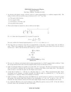
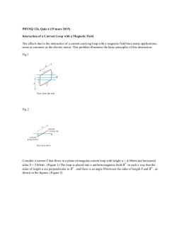


© Copyright 2026