
Design and characterisation of an AES chip - HAL-EMSE
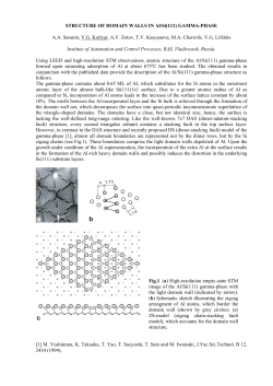
Design and characterisation of an AES chip embedding
countermeasures
Michel Agoyan, Sylvain Bouquet, Jean-Max Dutertre, Jacques Jean-Alain
Fournier, Jean-Baptiste Rigaud, Bruno Robisson, Assia Tria
To cite this version:
Michel Agoyan, Sylvain Bouquet, Jean-Max Dutertre, Jacques Jean-Alain Fournier, JeanBaptiste Rigaud, et al.. Design and characterisation of an AES chip embedding countermeasures. International Journal of Intelligent Engineering Informatics, 2011, pp.00. <emse00624400>
HAL Id: emse-00624400
http://hal-emse.ccsd.cnrs.fr/emse-00624400
Submitted on 16 Mar 2015
HAL is a multi-disciplinary open access
archive for the deposit and dissemination of scientific research documents, whether they are published or not. The documents may come from
teaching and research institutions in France or
abroad, or from public or private research centers.
L’archive ouverte pluridisciplinaire HAL, est
destin´ee au d´epˆot et `a la diffusion de documents
scientifiques de niveau recherche, publi´es ou non,
´emanant des ´etablissements d’enseignement et de
recherche fran¸cais ou ´etrangers, des laboratoires
publics ou priv´es.
Design & characterisation of an AES chip
embedding countermeasures
Michel Agoyan1 , Sylvain Bouquet1 , Jean-Max Dutertre2 , Jacques Fournier*1 ,
Jean-Baptiste Rigaud2 , Bruno Robisson1 , Assia Tria1
1
CEA-LETI Minatec
E-mail: [email protected] *Corresponding author
2
Ecole Nationale Sup´erieure des Mines de Saint Etienne
E-mail: [email protected]
CMPGC, 880 route de Mimet 13541 Gardanne, France
Abstract. In critical communication infrastructures, hardware accelerators are often used to speed up cryptographic calculations. Their resistance to physical attacks determines how secure the overall infrastructure is. In this paper, we describe the implementation and characterisation of an AES accelerator embedding security features against physical attacks. This AES chip is implemented in HCMOS9gp 130nm STM
technology. The countermeasure is based on duplication and works on
complemented values in parallel. The chip was tested against side channel attacks showing the efficiency of the proposed countermeasure against
such attacks. Fault injection tests based on the use of local laser shoots
showed that the fault detection mechanism did indeed react as expected. However, using clock set-up time violations, 80% of the secret
key were retrieved in less than 40 hours, thus illustrating the limits of
the duplication counter-measure against a global fault attack which was
published after the chip was designed.
Advanced Encryption Standard; Side channel analysis; Circuit duplication;
Dual representation; Fault detection and propagation; Fault attacks.
1
Introduction
Security in communication systems has become mandatory in many ubiquitous communication infrastructures. Whether it is for the confidentiality, authenticity and integrity of electronic financial transactions or e-government or
for the privacy of the end-users, security tools are being massively deployed
in equipments like mobile phones or laptops. Moreover, “civil” communication
infrastructures are growingly being eyed for the deployment of critical infrastructures: for example in the EU SECRICOM initiative [SECRICOM (2008)],
a secure communication infrastructure is developed over existing “civil” technologies for cross-border crisis management. In such secure infrastructures, the
use of a hardware module to manage secret keys, accelerate cryptographic algorithms and manage access rights has been defined. As the security of the system
depends on the security of its weakest link, the security of such hardware modules against physical attacks has become a critical feature for the successful
deployment of the secure communication infrastructure.
In this article, we focus on the design of embedded cryptographic accelerators, specially on the countermeasures that can be used to increase their resistance against physical attacks and ways and methods to evaluate the efficiency
of such countermeasures. Our case study is based on the implementation and
security characterisation of a hardware accelerator for the Advanced Encryption Standard. We propose a new design approach to thwart both side-channel
and fault attacks, two of the most dangerous physical attacks against cryptographic implementations. We then describe the physical tests done to evaluate
the resistance of the fabricated chip to illustrate the efficiency (against attacks
that were known at design time) and limits (against attacks which were not yet
published at design time) of the proposed countermeasures. We then discuss
about the analysis made out of the test results.
2
2.1
Cryptography, physical attacks and counter-measures
Cryptographic algorithms
Cryptography, as used in protocols like TLS [OpenSSL (2000)], can be described
as the art of transforming input data, called a message, into an output, called a
cipher, sometimes using a secret key: knowing the cipher, no information can be
inferred about the message. There are several types of cryptographic functions.
Hash functions transform data of arbitrary length into a hash of fixed length
[NIST (2002)]. Secret Key algorithms use a secret key to encrypt a message and
the same key to decrypt the corresponding cipher : the message and cipher are
of same length which is defined arbitrarily in Stream ciphers (where each bit is
encrypted individually) or as blocks of fixed sizes as in Block ciphers (examples
of Block ciphers are the DES (Data Encryption Standard) [NIST (1993)] or
the AES (Advanced Encryption Standard) [NIST (2001)]). Asymmetric cryptography or Public Key algorithms use two keys: a public one used for encryption and a private one used for decryption. Examples of PK algorithms are the
RSA [Rivest et al. (1978)] and Elliptic Curve Cryptography (ECC) [Blake et al.
(1999)].
2.2
Attacks & counter-measures
Even though cryptographic algorithms like AES or RSA are mathematically
robust, their implementation can be subjected to physical attacks when the attacker has physical access to the security device. We first have invasive attacks
where the attacker tries to directly observe the signals from within the chip
(through techniques like micro-probing) or read the bits from within the memories themselves or to use tools like a FIB (Focussed Ion Beam) to short-circuit
some of the security sensors of the circuit or re-connect some other parts which
had intentionally been disconnected for security purposes [Walker and AlibhaiSanghrajka (2004); Anderson and Kuhn (1997)]. Such attacks, due to their prohibitive cost and destructive nature are of lesser interest to us. We mainly focussed on non-invasive or “semi-invasive” attacks like side channel attacks and
fault attacks.
For attacks based on side channel information leakage, information about
the internal processes of the chip and the data manipulated can be derived by
observing external physical characteristics of the chip (like the power consumed
or the electromagnetic waves emitted or the time taken by a given process).
In Timing Attacks [Kocher (1996); Dhem et al. (1998)], by observing the time
taken by a “na¨ıve” implementation of a cryptographic algorithm (say RSA), one
can determine the bit values of the secret key manipulated. In another class of
attack called Simple Power Analysis, by observing the power profile of the chip
during such a calculation, one can derive information about the secret key bits
used. Power Analysis attacks were first published in [Kocher et al. (1999)] and
since then side channel attacks have been a major concern to the hardware security world. Differential Power Analysis mainly targets secret key algorithms
based on the fact that for each bit of the secret key, the power consumed by a
0 is different from the power consumed by a 1 (corresponding to the “Hamming
Weight”, i.e. the number of ones, leakage model). Later, researchers showed
that electromagnetic radiation from a chip could also be used as a source of
side-channel [Gandolfi et al. (2001); Quisquater and Samyde (2001)]. Different
leakage models have further been proposed when doing differential side channel analysis. For example, “Hamming Distance” (i.e. the number of positions for
which the bits have “flipped”) models have been put forward in [Mayer-Sommer
(2000)]. Correlation Power Analysis or Mutual Information Analysis have been
proposed to quantitatively test the dependency between the side channel measured and the data being manipulated by a security device [Brier et al. (2004);
Gierlichs et al. (2008)].
Another class of attacks are fault attacks where an attacker will try to modify the data handled by a chip or corrupt the processor’s execution flow at a
specific time of a cryptographic calculation. From the results of a correct execution and those of a corrupted execution, the attacker then tries to retrieve
part or all of the secret key by using techniques like Differential Fault Analysis
(DFA) [Biham and Shamir (1997)]. Such attacks have particularly been tested
on block ciphers like AES as described in [Piret and Quisquater (2003); Giraud
(2005)]. Another class of attacks called safe error attacks consists in the extraction of secret keys from the behaviour of the chip in the presence of a fault
[Yen and Joye (2000); Robisson and Manet (2007)]. To inject faults, an attacker
can for example generate glitches on the power supply, cause clock set-up time
violations on the input clock [Removed for Review ] or irradiate the chip with
a laser or light source [Skorobogatov and Anderson (2002)]. Fault attacks can
also be used to corrupt the correct flow of a program in order to make it take a
given branch of the program [Choukri and Tunstall (2005)] or to cause memory
dumps.
Several countermeasures have been proposed in the literature. Those which
target side channel attacks consist in either reducing the informative signal (i.e.
the physical characteristics which are correlated with the sensitive data), or
adding noise to blur the measurements. The informative signal has been reduced, for example, by using power filters or electromagnetic shields or by using “balanced” logic. Balancing may consist in rendering the Hamming Weight
(HW) of sensitive internal data constant. The 1-out-of-N encoding of these data
is a widespread technique to achieve this. The encoding obtained with N=2
is called “dual-rail” encoding. This countermeasure approximately doubles the
size of chip. Balancing may also consist in rendering the Hamming Distance
(HD) of sensitive internal computations constant, for example, by using both
the 1-out-of-N encoding and a dedicated communication protocol between the
different parts of the circuit. The more widespread ones insert spacers (i.e. a
constant value which does not carry information) between values. When the
spacer is equal to zero, the protocol is called “return-to-zero” (RTZ). Roughly,
this countermeasure halves the performances of the chip by a factor 2. Many
implementations attempting to balance HW and HD have been proposed at different levels of abstraction ([Tiri and Verbauwhede (2003); Soares et al. (2008)]
at gate level, [Ambrose et al. (2011)] at the architecture level and even at software level [Chen et al. (2010)]). The last step consists in physically balancing
the propagation of the encoded values between the different parts of the circuit,
for example, by using ad hoc Place and Route (P&R) techniques [Guilley et al.
(2005)]. A fair comparison between some balancing techniques is proposed in
[Guilley et al. (2010)]. Moreover noise can be added, for example, by randomizing the order of the instructions, by adding dummy operations or by masking
the internal computations that can be predicted by the attacker [Akkar and
Giraud (2001); Tokunaga and Blaauw (2009)].
The countermeasures against fault attacks consist either in detecting errors
during the computation and then taking actions to protect data or in making
the circuit less sensitive to fault injections. The detection of error is mainly
based on information redundancy either in space (doing the same computation
several times in parallel) or in time (repeating the same computation several
times) [Bertoni et al. (2002); Karri et al. (2003); Karpovsky et al. (2004)]. Several sensors have also been proposed to detect abnormal modifications of the
chip’s environment (voltage, temperature, clock frequency, light, etc.). Once a
fault has been detected, one reaction may consist in temporarily stopping the
communication with the outside (the chip “mutes”) and/or resetting parts of
the running software. The ultimate reaction consists in permanently destroying
all the (sensitive) data stored in the chip. In order to render the circuit less
sensitive to faults, redundancy is mainly used (one thus speaks of “error correction”). But the required level of redundancy is high: the computation has to be
performed at least three times.
However, few attempts have been made to propose a solution that thwarts
both classes of attacks. Asynchronous design techniques [Moore et al. (2003);
Kulikowski et al. (2006); Bastos et al. (2009)] have been touted as offering pro-
tection to side-channel and fault attacks because “by construction” they embed
RTZ and dual-rail encoding and because the handshake protocol of communication between the different parts of the circuit decrease the susceptibility to fault
attacks. The limits of such countermeasures have been reported in [Fournier
et al. (2003)].
In our paper, we handle both side channel and fault attacks by proposing an architecture based on duplicated-complemented (also called ‘dual’) data
paths applied to the AES algorithm. The dual data paths balance the Hamming
Weight and are also used to detect faults.
3
3.1
Design of the AES accelerator
The Advanced Encryption Standard
M0 M1 M2 M3
K0
K1 K2 K3
Input
MESSAGE
Input
KEY
TRANSFORM K3 -->T3
SUB-BYTES
T3
K0
K’0
K1
K’1
K2
K’2
K3
KEY_EXPANDER #1
SHIFT_ROWS
RND_EXE 1
MIX_COLUMNS
K’0
K’1
K’2
K’3
SUB-BYTES
SHIFT_ROWS
RND_EXE 9
MIX_COLUMNS
KEY_EXPANDER #10
SUB-BYTES
SHIFT_ROWS
Output
CIPHER
C0
C1 C2 C3
Fig. 1. Structure of the 128-bit AES
The structure of the 128-bit-key AES [NIST (2001)] (or AES-128) is illustrated in Figure 1. The 128-bit data or key are considered as a matrix of 4 × 4
bytes. The algorithm itself consists of a building block, called RND EXE executed
iteratively 10 times. The RND EXE function consists of the following basic operations:
– SUB-BYTES is a non-linear transformation working independently on individual bytes of the matrix consisting of a Galois Field inverse calculation
followed by an affine transformation.
– SHIFT ROWS is a simple rotation operation on each row of the data matrix.
– MIX COLUMNS is a linear matrix multiplication working on each column where
multiplications are done in GF(28 ).
– ADD-RND-KEY, illustrated in Figure 1 by the XOR symbol, consists of a bytewise XOR between the data matrix and the corresponding sub-key matrix.
Independently from these, the KEY EXPANDER module iteratively calculates
sub-keys for the ADD-RND-KEY function. The KEY EXPANDER for a key size of 128
bits is shown in the right part of Figure 1. The TRANSFORM operation done on
the forth column of the key (K3) is detailed in [NIST (2001)].
3.2
Architecture of the TR-AES
Fig. 2. Architecture of the secure AES chip
Our design (which we shall call the Tamper Resistant AES, TR-AES) aims
to protect against both DFA and side channel attacks. In our case, performance prevails over surface as the module was originally designed to encrypt
data transfers between two devices. The countermeasure against DFA consists
first in detecting errors and then reacting in case of detection. In order to obtain a reasonable fault-coverage for an acceptable surface penalty, we chose, as
suggested in [Malkin et al. (2005)], to detect errors by using spatial duplication:
the AES-128 is executed twice in parallel. At each step (or round) of the algorithm, the consistency between the results of the two instances of the algorithm
is checked. Several reactions in case of attacks have been analysed. For example, we could have returned a constant value instead of the faulty cipher or to
return a random value. We have excluded the first solution because we considered that it could open a breach to safe-error attacks and the second because we
have no available true random number generator. In order to mimic the effect
of such random generator, the chosen strategy of reaction consists in blurring
the erroneous cipher-text with the scrambled value of the detected error, as explained in [Joye et al. (2007)]. In order to counter side channel attacks, the two
different instances of the algorithm are designed such that when a bit of each
intermediate value is computed in one instance, the other instance computes
the complemented values. This trick creates dual data channels when considering the two instances. One is called the ‘original path’, the other is called
the ‘complemented or dual path’. The logic gates used in the two instances are
also “complemented”, i.e. the XOR gates from the original path are replaced
by XNOR gates. Note also that, because we did not want to reduce the performance of the circuit, we did not insert spacers for balancing the HD. No
particular constraints have also been applied during the P&R step.
The resulting architecture is shown in Figure 2. To obtain the best performances, the RND EXE function, the KEY EXPANDER are computed in parallel with
128-bit data paths. Each round is executed in one clock cycle. As the consistency of data is tested on the outputs of the SUB-BYTES module (the upper part
of Figure 4), the latency of detection of error is also of one clock cycle. Figure 3
details the error detection and propagation. Further spreading of the errors is
achieved by cross-changing wires between the original and the dual data paths
at the level of the SHIFT ROWS module. Figure 4 illustrates what happens when
an error is generated at the beginning of the last round on one of the data
paths.
3.3
The final AES chip
The TR-AES was designed with the standard cells of the HCMOS9gp 130nm
STM technology. The TR-AES typically works at 1.20V and its maximum frequency is 50MHz at 27 ◦ C. The resulting die is 1336µm × 1411.8µm in size, due
to the limitation by the 52 pads of the ring (Figure 5). The AMBA APB interface consists of 32 bidirectionnal I/Os and 4 bits of address. The AES functional
block itself uses 27000 gates corresponding to an area of 0.165mm2 (including
the communication interface) which represents an overhead of 67% when compared to a non-secure AES in the same technology (16500 gates). Different analyses have been performed to detect potential security flaws at design-time. The
method used to detect weaknesses against side-channel attacks and the results
obtained for the TR-AES are described in [Laabidi (2010)]. We have verified
that, thanks to the search for correlations between bits in the RTL description
of the TR-AES, each bit in the original path is balanced by its dual counterpart.
Mi
Mi
mij ⊕ e
mij
Mi ⊕ Mi
aij = 0 ou aij = e
aij
0
Error State
E
cj =
e
einv
ri =
P
j=0..3
aij
i=0..3
aij
P
eij = ri + cj
eij
Inv bits
Einv
Fig. 3. Error Matrix Calculation
But thanks to this method, we have also detected some very slight differences in
the structure of the two instances of the algorithm when they are described at
gate level. In order to estimate the associated threat, side channel attacks have
been performed on the simulations of the power consumption (obtained with
simple toggle counts). These simulations showed that the tiny difference which
may appear on the power consumption of the two instances of the algorithm
are mainly due to the difference of delay of propagation of a bit and its dual
counterpart. Manual modifications of the design at gate level have been done
in order to suppress these differences: for example we made sure the entities of
both data paths were synthesized using the same types of logic gates.
4
Side-channel analysis of the AES
We first tested the TR-AES chip against side channel attacks. To start with, we
took a quick look at what the standard deviation of the measured side-channel
curves looked like: Figure 6 shows that while we have significant variations during the data transfers (that of the cipher for example), the variations seen during the AES calculation itself is close to “noise” levels. This was the first hint
that our design choices reduced side channel information leakage.
We observed both the power consumed and the EM waves emitted by the
TR-AES during an encryption process and we tried to carry correlation analysis (CPA/CEMA) [Brier et al. (2004); Gandolfi et al. (2001)]: for each byte
Dual Path
Original Path
Fault
injected
on one
byte
M9
M9
SBdual
SB
Error
Detection
Matrix
Sub-Bytes
Error
Matrix
Calculation
Error
Matrix
Shift-Rows
K10
K10
Faulted byte
Fig. 4. Fault on one ‘data path’ is generated & propagated
of the intermediate data matrix of 4 × 4 bytes, we calculate correlation curves
between the power/EM traces and the Hamming Weight of the intermediate
values (analyses were done both for intermediate values output from the first
ADD-RND-KEY and of the SUB-BYTES of the first round) for each of the 256
possible values of the sub-key byte. When the attack works (on a non protected
AES implementation for example), the correct sub-key byte is thus obtained
for the correlation curve which has the highest peak compared to the other
ones (Figure 7). On the TR-AES, despite using a large number of curves (approximately 1,000,000 acquisitions), no significant data dependant leakage has
been found (Figure 8).
Concerning the EM measurements, they were done in a more localised way,
providing curves with better signal-to-noise ratios than for power measurements.
We used a horizontal probe with a diameter of 150µm. We first identified the
regions of the chip where the most significant data dependant variances were
seen in the measured EM waves. For each of those regions, we carried Correlation EMA attacks.
We further tried different leakage models (for example targeting bits or bytes
of the secret keys) but in vain. Those results illustrate the efficiency of the
“dual” data representation of the TR-AES against power and EM attacks which
have been proven to work on non-secure implementations of the AES.
Fig. 5. Picture of the fabricated AES chip
5
5.1
Resistance of the AES against fault attacks
Local laser-based fault injection attacks
We also tested the TR-AES against fault attacks. The first injection means used
is a green laser source whose wavelength (532nm) has proven to be efficient for
front-side injections [Agoyan et al. (2010a)]. Preliminary tests were done with
the energy set close to its minimum available value in the nano-Joule range to
avoid damaging the chip and also to try to generate the least number of errors.
The spot size was set around 50µm to allow a quick inspection of the chip area.
Depending on the spatial and the temporal location of the laser shoot, different
behaviours were observed. When the state machines of the AES module itself
or the communication interface were affected, the communication with the chip
was lost. Hitting the RND EXE or KEY EXPANDER modules lead to the output of
massively faulted cipher-texts. To gain more insight into how to fine-tune precisely the laser energy and spot size to obtain faults restrained to a single byte,
we targeted the last round. Even though there are, to our best knowledge, no
published attacks on faults injected during the last AES round, these experiments allowed us to obtain the settings enabling the injection of single byte
faults (a spot size of 6 − 12µm and an energy between 0.2 and 5 nJ) and the location of the design’s sensitive areas. To establish the efficiency of the detection
mechanism, the laser pulses were operated in the time range of the penultimate
AES round and on areas of the die corresponding to the ADD-RND-KEY and to
the input registers of the SUB-BYTES module (see Figure 2).
We practically produced the effect illustrated in Figure 4: fault detection
and error spreading. The laser injected faults (even single bit faults in some
cases) during the AES calculation but the error was spread by our mechanism:
Fig. 6. Standard deviation on power curves for 1000 different messages
faults induced into one byte of the intermediate values at the beginning of a
given round are spread across at least seven other bytes at the end of the same
round. However, the actual implementation suffers from a flaw: six out of the
seven faulty bytes will reveal the original fault itself (in reverse bit order) when
XORing with the correct cipher-text. That information leakage may ease the recovery of the secret key. Nevertheless, as stated in Section 3.2, what we intended
to validate is the efficiency of the detection mechanism. To proceed, more than
5, 000 injection experiments were carried out on the RND EXE and KEY EXPANDER
modules during the ante-penultimate and penultimate rounds. None of the obtained faults was able to defeat the detection mechanism. This validates the
efficiency of our countermeasure’s detection mechanism against laser induced
faults.
5.2
Global clock-glitch-based fault injection attacks
Since the TR-AES chip works with an external clock, we chose to stress-test the
circuit using the clock set-up time violation fault injection technique described
in [Agoyan et al. (2010b)]: we decrease the clock period at a targeted cycle in
order to corrupt the execution of one particular round of the AES. This faulty
clock is generated using the embedded Delay Locked Loop (DLL) of a Xilinx
Virtex 5 FPGA. Two clocks (clkd1 and clkd2) with programmable skews are
generated from the original 50MHz clock (clk) and the resulting faulty period
is a combination of clkd2’s rising edge and clkd1’s falling edge (Figure 9). The
generated clock’s skew ∆T varies from 0 to ∆Tmax = 9804ps by steps of δT =
76ps (the DLL’s smallest elementary delay). Hence, the period of the faulty
Fig. 7. Correlation curves obtained from a CPA on a non-protected AES
Fig. 8. Correlation curves obtained from CPA on our secure AES
clock cycle varies between 10.196ns and 20ns. In [Agoyan et al. (2010b)], the
authors generated single bit faults on a non-secure FPGA implementation of
the AES by modifying the duration of the skew.
In order to exploit the generation of single bit faults on AES, we used two
differential fault cryptanalysis techniques where bytes of the 10th sub-key were
found. In the first one described in [Giraud (2005)], the attacker has to inject
only one bit error at the end of the 9th (one before last) round of the AES. Then
by using the expected cipher-text and the corrupted one, bits of the secret keys
can be found. For a given byte, with 3 corrupted cipher-texts, the corresponding
sub-key byte is found with a probability of 99%. The second technique is given
in [Piret and Quisquater (2003)]. There, a single byte fault has to be injected
at the end of the 8th round of the AES such that the correct cipher-text and
the faulty one differ by four bytes. With two faulty cipher-texts (resulting from
the same intermediate state corrupted by faults injected on the same column),
there are 97% chances of retrieving the corresponding column’s secret sub-key.
The TR-AES’s error detection and spreading mechanism was initially designed
to defeat these two differential cryptanalysis schemes.
For those two techniques to work on the TR-AES, we need to ‘bypass’ the
error detection. To achieve this, corresponding “dual” errors have to be generated on the ‘original’ and the ‘dual’ data paths as shown in Figure 10. Conse-
Tclk
clk
clkd1 ↓
clkd2 ↑
Faulty clk
Tclk - ∆T
Fig. 9. Faulty clock generation
quently the error matrix is null, the error is not detected and at the end of the
attacked round, only one byte is corrupted. A fault is hence generated and yet
not detected by the countermeasure.
We used the DLL-based clock set-up time violation board to inject the desired faults. The attack scenario used is given in Figure 11: for each of the different N random messages M, the skew on a ‘specific’ clock cycle (corresponding
to a round) is increased until the ‘attack condition’ is satisfied. In the case of
Giraud’s attack, the clock skew is inserted during the 9th round and the ‘attack
condition’ corresponds to having a faulty cipher-text with only one corrupted
byte. Out of N=60,000 executions, done in 36 hours, 235 cipher-texts had one
faulty byte and among these, 6 different bytes locations were impacted. This approach revealed bytes 5, 7, 8, 9 and 10 of the AES 10th sub-key and reduced to
3 the number of possibilities for the 1st one. For the Piret-Quisquater’s attack,
the skew is inserted during the 8th round and the ‘attack condition’ corresponds
to having an entire column of the cipher-text impacted. We played 20,000 scenarios (in 13 hours), 9 of which induced four-byte errors on a column but only
six were exploitable for the attack. We hence found bytes 2, 3, 4, 5, 6, 7, 9, 10,
12, 13, 15 and 16 of the 10th sub-key. By combining the results from both attacks we got 13 bytes of the 10th sub-key and had only 3 possibilities for a 14th
one. The remaining sub-key bits could then be found using 3 × 28 × 28 brute
force searches. With the 10th sub-key, the original secret key can be calculated
by executing the iterative KEY EXPANDER in the reverse order.
6
Discussion
The TR-AES’s error detection and spreading mechanism was supposed to offer a full fault resistant countermeasure. It was based on the assumption that
it was impossible to inject simultaneously the same fault (to be more specific,
complemented faults) on the ‘original’ data path and on the ‘dual’ one. A first
set of experiments, with a laser as a fault injection means, proves this assumption to be correct. This result was due to the nature of the laser beam we used,
which had only a local effect on the AES chip. However, our detection mech-
Dual Path
Original Path
Fault
injected
on one
byte
M9
M9
SBdual
SB
Error
Detection
Matrix
Sub-Bytes
Error
Matrix
Calculation
Error
Matrix
Shift-Rows
K10
K10
Faulted byte
Fig. 10. Faults generated on both paths without detection nor propagation
anism was defeated by the use of a fault injection means with a global effect:
glitching the clock to induce timing constraint violations. We originally thought
that it was impossible to inject the same fault in both paths. Nevertheless, we
have obtained, with a success rate of 4 in 10000, faulty cipher-texts where the
detection mechanism did not work. These faulty cipher-texts were successfully
used to recover the secret key according the aforementioned DFA schemes. As
a consequence, a new series of experiments was conducted to monitor the propagation delays (i.e. the critical times) of the original and dual data paths. The
experimental scheme was based on the one described in Figure 11, with the following differences: at each iteration, both the plain-text and key were changed
randomly, the ‘attack condition’ corresponding to the appearance of the first
single bit fault, N was set to 50,000, and the clock glitch was injected during
the penultimate round. Knowing the TR-AES architecture and both the key
and the plain-text, we were able to calculate from the resulting cipher-texts
the faults actually induced and their locations. Among them, 27,715 were single bit faults, and as a consequence, their corresponding times of occurrence
gave the critical times corresponding to the handled data. The critical times of
both original (left part) and dual (right part) data paths are reported in the
bar diagrams of Figure 12.
In both diagrams, the critical times are distributed on the same time range
of 11,500 to 13,100 ps. These distributions almost follow a Gaussian law. These
Init M, N
Set n = 0
Change M
Increase n = n + 1
Load M
Set ∆T = 0
Encrypt
C∆T = AESK (M )
Attack
conditions
satisfied ?
NO
Store Results
C0 , ∆T, M, C∆T
YES
n = N?
YES
End Test
NO
YES
∆T = ∆Tmax ?
NO
Increase ∆T
∆T = ∆T + δT
4000
400
3500
350
Number of occurence
Number of occurence
Fig. 11. Attack scheme for Giraud’s & Piret-Quisquater’s attacks
300
3000
250
2500
200
2000
150
1500
100
1000
50
500
0
0
11488
11792
12096
12400
Critical time (ps)
12704
13008
13312
11488
11792
12096
12400
12704
13008
13312
Critical time (ps)
Fig. 12. Number of measurements versus critical times for the original (left part,
dark grey) and dual (right part, light grey) data paths
plots reflect the data dependence of the propagation delays through logic gates.
The two distributions appearing on the same time range, it appears obvious
that we were able to inject single bit faults simultaneously on both data paths.
Then, from a statistical point of view, part of these faults had to be injected on
the same bytes locations (one draw out of 16) and actually to be the same (one
draw out of 255). This also reveals that the design of both data paths benefits
from a good timing equilibrium. We think that this observation can account for
the resistance of the chip to side channel attacks.
However, we call the reader’s attention to the scales of the y-axis: that of the
original data path is 10 times that of its dual counterpart (Figure 12). We expected them to be identical if the critical times of the two paths were the same.
The critical time was reached 25,353 times in the ‘original’ path and 2,362 times
in the ‘dual’ one.We explain this by a shadowing effect from the original data
path on its complemented counterpart while measuring the critical time experi-
mentally, the latter path having smaller critical times. We have mathematically
tested this hypothesis by considering that both data paths have Gaussian distributions. Figure 13 illustrates a model of the critical times distributions that
correspond to the results of Figure 12. This figure was drawn assuming that
we were able to measure both data paths’ propagation delays without suffering
from the shadowing effect. The critical times’ Gaussian distribution of the original data path has a mean of 12,400 ps, whereas the dual one has a mean of
11,850 ps. Their standard deviations are also different: 226 and 350 ps respectively for the original and dual data paths. The difference of their means, which
is 550 ps, explains the shadowing effect.
The countermeasure would have been efficient against ‘global’ fault attacks
if the two distributions did not intersect. However, such a modification would
break the equilibrium between the propagations delays, and as a consequence
would probably make side channel attacks feasible. This shows that there is
here a contradiction between hardening a design against ‘global’ fault injection
and protecting it against side channel attacks.
4000
3500
Number of occurence
3000
2500
2000
1500
1000
500
0
10348
10652
10956
11260
11564
11868
12172
12476
12780
13084
13388
13692
Critical time (ps)
Fig. 13. Rebuild of the distributions of the critical times of the original (dark grey)
and dual (light grey) data paths according a Gaussian law (without shadowing effect).
7
Conclusion
This paper describes an ASIC AES chip having a complemented duplicated
implementation which constitutes a countermeasure against both fault attacks
(detection via duplicated data paths and spreading of errors rendering the faulty
cipher-text useless to DFA) and side-channel attacks (working on complemented
data in parallel). Other design techniques like asynchronous circuits or DualRail (DR) encoding have tried to tackle both kinds of attacks in the same way.
Our approach is more cost efficient (only 67% overhead in our case on the whole
chip) and our tests show significant robustness to attacks (against side-channel
attacks and against ‘local’ laser fault attacks), which is not the case for the
others when referring to [Fournier et al. (2003)]. However, using clock set-up
time violations, we showed that such a counter-measure is not enough to protect against fault injections. With Giraud’s and Piret-Quisquater’s techniques,
13 out of 16 secret key bytes were retrieved in less than 40 hours. It is, to our
best knowledge, the first reported practical results on an AES ASIC chip showing that fault detection based on duplication can be defeated using low cost
techniques. This counter-measure was designed to resist to a laser beam fault
injection, which has a local effect, as opposed to a stress induced by a clock
glitch which has a global effect on both data paths. In the light of the data
retrieved from the fault attacks described in this paper, we believe that combined side-channel and fault attacks can be carried on such a design as further
investigation.
Acknowledgements
This work was funded by the SECRICOM project (EC FP7-SEC-2007 grant
218123).
Bibliography
Agoyan, M., J.-M. Dutertre, A.-P. Mirbaha, D. Naccache, A.-L. Ribotta, and A. Tria,
How to flip a bit?, in Proceedings of the 16th International On-Line Testing Symposium (IOLTS), pp. 235–239, IEEE, 2010a.
Agoyan, M., J.-M. Dutertre, D. Naccache, B. Robisson, and A. Tria, When clocks fail:
on critical paths and clock faults, in Proceedings of the 9th Smart-card Research
and Advanced Application Conference (CARDIS’10), edited by J.-L. L. Julien
Iguchi-Cartigny, Dieter Gollmann, vol. LNCS, pp. 182–193, Springer-Verlag, Germany, 2010b.
Akkar, M.-L., and C. Giraud, An Implementation of DES and AES, Secure against
Some Attacks, in Proceedings of the 3rd International Workshop on Cryptographic
Hardware and Embedded Systems (CHES’01), edited by C
¸ etin Ko¸c, D. Naccache,
and C. Paar, vol. 2162 of LNCS , pp. 309–318, Springer-Verlag, Paris, France,
2001.
Ambrose, J., R. Ragel, S. Parameswaran, and A. Ignjatovic, Multiprocessor information concealment architecture to prevent power analysis-based side channel
attacks, Computers Digital Techniques, IET , 5 (1), 1 –15, 2011.
Anderson, R., and M. Kuhn, Low Cost Attacks on Tamper-Resistant Devices, in
Security Protocols 5th International Workshop, edited by M. Lomas and al, no.
1361 in LNCS, pp. 125–136, Springer-Verlag, Paris, France, 1997.
Bastos, R. P., Y. Monnet, G. Sicard, F. L. Kastensmidt, M. Renaudin, and R. Reis,
Comparing transient-fault effects on synchronous and on asynchronous circuits.,
in IOLTS’09 , pp. 29–34, 2009.
Bertoni, G., L. Breveglieri, I. Koren, P. Maistri, and V. Piuri, A parity code based
fault detection for an implementation of the advanced encryption standard, in
DFT ’02: Proceedings of the 17th IEEE International Symposium on Defect and
Fault-Tolerance in VLSI Systems, pp. 51–59, IEEE Computer Society, Washington, DC, USA, 2002.
Biham, E., and A. Shamir, Differential Fault Analysis of Secret Key Cryptosystems,
in Proceedings of the 17th International Advances in Cryptology Conference –
CRYPTO’97 , no. 1294 in LNCS, pp. 513–525, 1997.
Blake, I., G. Seroussi, and N. Smart, Elliptic Curves in Cryptography, vol. 265 of
Lecture Note Series, London Mathematical Society, 1999.
Brier, E., C. Clavier, and F. Olivier, Correlation Power Analysis with a leakage
model, in Proceedings of the Workshop on Cryptographic Hardware and Embedded Systmes (CHES 2004), edited by M. Joye and J.-J. Quisquater, vol. 3156 of
Lecture Notes in Computer Science, pp. 16–29, Springer-Verlag, 2004.
Chen, Z., A. Sinha, and P. Schaumont, Implementing virtual secure circuit using a
custom-instruction approach, in Proceedings of the 2010 international conference
on Compilers, architectures and synthesis for embedded systems, CASES ’10, pp.
57–66, ACM, New York, NY, USA, 2010.
Choukri, H., and M. Tunstall, Round Reduction Using Faults, in 2nd Workshop on
Fault Diagnosis and Tolerance in Cryptography (FDTC 05), pp. 13–24, Edinburgh, Scotland, 2005.
Dhem, J.-F., F. Koene, P.-A. Leroux, P. Mestr´e, J.-J. Quisquater, and J.-L. Willems,
A Practical Implementation of the Timing Attack, in Proceedings of the 3rd
Smart-card Research and Advanced Application Conference (CARDIS’98), edited
by J.-J. Quisquater and B.Schneier, no. 1820 in LNCS, pp. 167–182, SpringerVerlag, UCL, Louvain-la-Neuve,Belgium, 1998.
Fournier, J. J., S. Moore, H. Li, R. Mullins, and G. Taylor, Security Evaluation
of Asynchronous Circuits, in Proceedings of the 5th International Workshop on
Cryptographic Hardware and Embedded Systems (CHES’03), edited by C. Walter
and al., no. 2779 in LNCS, pp. 137–151, Springer-Verlag, Cologne, Germany,
2003.
Gandolfi, K., C. Mourtel, and F. Olivier, Electromagnetic Analyis: Concrete Results,
in Proceedings of the 3rd International Workshop on Cryptographic Hardware and
Embedded Systems (CHES’01), edited by C
¸ etin Ko¸c, D. Naccache, and C. Paar,
vol. 2162 of LNCS , pp. 251–261, Springer-Verlag, Paris, France, 2001.
Gierlichs, B., L. Batina, P. Tuyls, and B. Preneel, Mutual Information Analysis A Generic Side-Channel Distinguisher, in Cryptographic Hardware and Embedded
Systems - CHES 2008 , edited by E. Oswald and P. Rohatgi, vol. 5154 of Lecture
Notes in Computer Science, pp. 426–442, Springer-Verlag, Washington DC,US,
2008.
Giraud, C., DFA on aes, in Advanced Encryption Standard - AES , edited by H. Dobbertin, V. Rijmen, and A. Sowa, vol. 3373 of Lecture Notes in Computer Science,
pp. 27–41, Springer Berlin / Heidelberg, 2005.
Guilley, S., P. Hoogvorst, Y. Mathieu, and R. Pacalet, The “backend duplication”
method, in CHES’05 , pp. 383–397, 2005.
Guilley, S., L. Sauvage, F. Flament, V.-N. Vong, P. Hoogvorst, and R. Pacalet, Evaluation of power constant dual-rail logics countermeasures against DPA with design
time security metrics, IEEE Trans. Computers, 59 (9), 1250–1263, 2010.
Joye, M., P. Manet, and J.-B. Rigaud, Strengthening Hardware AES
Implementations against Fault Attack, IET Information Security, 1 , 106–
110, 2007.
Karpovsky, M. G., K. J. Kulikowski, and A. Taubin, Robust protection against fault
injection attacks on smart cards implementing the Advanced Encryption Standard, in 2004 International Conference on Dependable Systems and Networks
(DSN 2004), pp. 93–101, IEEE Computer Society, 2004.
Karri, R., G. Kuznetsov, and M. Goessel, Parity-Based Concurrent Error Detection
of Substitution-Permutation Network Block Ciphers, in Proceedings of the
5th International Workshop on Cryptographic Hardware and Embedded Systems
(CHES’03), edited by C. Walter and al., no. 2779 in LNCS, pp. 113–124,
Springer-Verlag, Cologne, Germany, 2003.
Kocher, P., Timing Attacks on Implementations of Diffie-Hellman, RSA, DSS and
other systems, in Proceedings of Advances in Cryptology (CRYPTO’96), LNCS,
pp. 104–113, Springer-Verlag, 1996.
Kocher, P., J. Jaffe, and B. Jun, Differential Power Analysis, in Proceedings of the
19th International Advances in Cryptology Conference (CRYPTO’99), no. 1666
in LNCS, pp. 388–397, Springer-Verlag, 1999.
Kulikowski, K., A. Smirnov, and A. Taubin, Automated design of cryptographic
devices resistant to multiple side-channel attacks, in Proceedings of 8th Workshop on Cryptographic Hardware and Embedded Systems (CHES’06), edited by
L. Goubin and M. Matsui, no. 4249 in LNCS, Springer-Verlag, Yokohama, Japan,
2006.
Laabidi, S., M´ethodologie de conception de composants int´egr´es prot´eg´es contre les
attaques par corr´elation, Ph.D. thesis, Ecole Nationale Sup´erieure des Mines de
Saint-Etienne, 2010.
Malkin, T. G., F.-X. Standaert, and M. Yung, A comparative cost/security analysis of fault attack countermeasures, in Second Workshop on Fault Detection and
Tolerance in Cryptography, pp. 109–123, Edinburgh, UK, 2005.
Mayer-Sommer, R., Smartly analyzing the simplicity and the power of simple power
analysis on smartcards, in Proceedings of the 2nd International Workshop on
Cryptographic Hardware and Embedded Systems (CHES’00), edited by C. Koc
and C. Paar, no. 1965 in LNCS, pp. 78–92, Springer-Verlag, Worcester, USA,
2000.
Moore, S., R. Anderson, R. Mullins, G. Taylor, and J. Fournier, Balanced selfchecking asynchronous logic for smart card applications, Microprocessors and Microsystems Journal (IEEE), 27 (9), 421–430, 2003.
NIST, Data Encryption Standard (DES), Tech. Rep. FIPS PUB 46-2 , Federal Information Processing Standards, 1993.
NIST, Specification for the Advanced Encryption Standard, Tech. Rep. FIPS PUB
197 , Federal Information Processing Standards, 2001.
NIST, Secure Hash Standard, Tech. Rep. FIPS PUB 180-2 , Federal Information Processing Standards, 2002.
OpenSSL,
Cryptographic
libraries
for
OpenSSL,
http://www
.openssl.org/docs/crypto/crypto.html, 2000.
Piret, G., and J.-J. Quisquater, A Differential Fault Attack Technique against SPN
Structures, with Application to the AES and KHAZAD, in Proceedings of the
5th International Workshop on Cryptographic Hardware and Embedded Systems
(CHES’03), edited by C. W. et al, no. 2779 in LNCS, pp. 77–88, Springer-Verlag,
2003.
Quisquater, J.-J., and D. Samyde, Electromagnetic Analysis (EMA): Measures and
coutermeasures for smart cards, Smart Card Programming and Security (e-smart
2001), LNCS (2140), 200–210, 2001.
Rivest, R. L., A. Shamir, and L. Adleman, A method for obtaining digital signatures and public-key cryptosystems, Communications of the ACM , 21 (2), 120–
126, 1978.
Robisson, B., and P. Manet, Differential behavioral analysis, in CHES , edited by
P. Paillier and I. Verbauwhede, vol. 4727 of Lecture Notes in Computer Science,
pp. 413–426, Springer, 2007.
SECRICOM,
Seamless
communication
for
crisis
management,
http://www.secricom.eu/menu-objectives, 2008.
Skorobogatov, S., and R. Anderson, Optical Fault Induction Attacks, in Proceedings of the Workshop on Cryptographic Hardware and Embedded Systmes (CHES
2002), edited by B. Kaliski and al., no. 2533 in LNCS, pp. 2–12, Springer-Verlag,
2002.
Soares, R., N. Calazans, V. Lomn´e, P. Maurine, L. Torres, and M. Robert, Evaluating
the robustness of secure triple track logic through prototyping, in Proceedings of
the 21st annual symposium on Integrated circuits and system design, SBCCI ’08,
pp. 193–198, ACM, New York, NY, USA, 2008.
Tiri, K., and I. Verbauwhede, Securing Encryption Algorithms against DPA at
the Logic Level: Next Generation Smart Card Technology, in Proceedings of
the 5th International Workshop on Cryptographic Hardware and Embedded Systems (CHES’03), edited by C. Walter and al., no. 2779 in LNCS, pp. 125–136,
Springer-Verlag, Cologne, Germany, 2003.
Tokunaga, C., and D. Blaauw, Secure aes engine with a local switched-capacitor current equalizer, in Solid-State Circuits Conference - Digest of Technical Papers
(ISSCC 2009), IEEE International, pp. 64–65, San Francisco, USA, 2009.
Walker, J. F., and A. Alibhai-Sanghrajka, Using FIB to hack security chips,
European Focused Ion Beam Users Group (EFUG 2004) presentation,
http://www.imec.be/efug/EFUG20h.html, 2004, SiVenture, Maidenhead, UK.
Yen, S.-M., and M. Joye, Checking before output may not be enough against faultbased cryptanalysis, IEEE Transactions on Computers, 49 (9), 967–970, 2000.


© Copyright 2026