
Cascaded Converters with Gate-Commutated Thyristors
Cascaded Converters with Gate-Commutated
Thyristors
Experimental Verification and Auxiliary Power Supply
TOMAS MODEER
Doctoral Thesis
Stockholm, Sweden 2015
TRITA-EE 2015:021
ISSN 1653-5146
ISBN 978-91-7595-581-0
KTH School of Electrical Engineering
SE-100 44 Stockholm
SWEDEN
Akademisk avhandling som med tillstånd av Kungl Tekniska högskolan framlägges till
offentlig granskning för avläggande av teknologie doktorsexamen Måndagen den 8:e
Juni 2015 klockan 10.15 i Kollegiesalen, Kungl Tekniska Högskolan, Brinellvägen 8,
Stockholm.
© Tomas Modeer, April 2015
Tryck: Universitetsservice US AB
Abstract
This thesis describes an effort to investigate the use of gate-commutated thyristors (GCTs) in cascaded converters. Cascaded converters, such as modular
multilevel converters (M2Cs) and cascaded H-bridge converters (CHBs), have
proved to be especially suitable in high-voltage, high-power applications. All
of the most important advantages of cascaded converters, e.g. redundancy and
scalability, can be attributed to the modular structure. Of special interest
regarding the choice of semiconductor power devices is the reduced requirement
on the switching frequency of individual devices. This brings a shift in the
trade-off between switching and conduction losses, where the latter has more
importance in cascaded converters than in other topologies. This shift favors
thyristor-type devices like the GCT, which can achieve very low conduction
losses.
To quantify the potential gain in the application of GCTs in cascaded
converters the losses have been calculated and a comparison between different
submodule implementations has been presented. The comparison has shown
that GCTs can provide 20-30% lower losses compared to insulated-gate bipolar
transistors (IGBTs) in a typical HVDC application. In order to verify the low
losses of GCT-based submodules, extensive work has been put into building
and testing full-scale submodules employing GCTs. A resonant test circuit
has been developed in which the submodules can be tested in steady-state
operation which allows calorimetric measurements of the losses. The calorimetric measurements have verified that the loss calculation was reasonable
and not lacking any important components.
A drawback of GCTs is that the gate-drive units require much more power
than gate-drive units for comparable IGBTs. In order to employ GCTs in
high-voltage cascaded converters some means of supplying this power in the
submodule must be provided. One option is to take this power from the
submodule dc-link, but this requires a dc-dc converter capable of high input
voltages. A tapped-inductor buck converter with a novel, autonomous highside valve was developed for this application. The autonomous operation of the
high-side valve allows reliable operation without galvanic isolation components.
A converter with a high-side valve with series-connected MOSFETs capable of
an input voltage of 3 kV has been presented.
Sammanfattning
Denna avhandling beskriver arbete som syftat till att undersöka möjligheten att använda gate-kommuterade tyristorer (gate-commutated thyristors,
GCT) i kaskad-kopplade omvandlare. Kaskad-kopplade omvandlare, t.ex. i
modulära multi-nivå omvandlare (modular multilevel converter, M2C) och
kaskad-kopplade H-bryggor (cascaded H-bridge, CHB), har visat sig särskilt
lämpade för tillämpningar med hög effekt och spänning. Denna typ av omvandlare har en mängd fördelar, såsom redundans och skalbarhet, som beror
av dess modulära struktur. Av särskilt intresse vad gäller valet av halvledare
är ett minskat behov av kommuteringar hos de enskilda ventilerna. Detta
ger en förskjutning i balansen mellan kommuterings- och led-förluster, där de
senare har större vikt i kaskadkopplade omvandlare än i andra omvandlare.
Detta gynnar halvledarventiler av tyristor-typ såsom GCTer, eftersom dessa
kan ge väldigt låga ledförluster.
För att kvantifiera hur stor förlustbesparing GCTer kan ge i kaskadkopplade omvandlare har en förlustberäkning utförts och en jämförelse mellan
olika submodulkonstruktioner presenterats. Jämförelsen har visat att GCTer
kan ge 20-30 % lägre förluster än IGBTer i en typisk HVDC-tillämpning. För
att verifiera att så verkligen är fallet, har mycket av arbetet fokuserat på att
bygga submoduler med GCTer i fullskala samt att utveckla en testkrets för
att kunna testa submodulerna i fortvarighet. Kalorimetriska mätningar på
denna testkrets har visat att de förlustberäkningar som utförts är riktiga och
att inga förlustkomponenter av större vikt har utelämnats.
En nackdel med GCTer är att gate-drivdonen kräver mer effekt än gatedrivdon för IGBTer i motsvarande effektklass. För att kunna använda GCTer
i kaskadkopplade omvandlare måste något sätt att tillhandahålla denna effekt
lokalt i submodulen ordnas. En tapped-inductor dc-dc-omvandlare med en ny,
autonom, ventilkonstruktion har utvecklats för detta ändamål. Detta ger en
tillförlitlig omvandlare utan behov av komponenter för galvanisk isolation.
Acknowledgment
This thesis concludes the work I have carried out at the Department of Electrical
Energy Conversion, KTH Royal Institute of Technology since May 2010. First of all
I would like to thank my supervisors Hans-Peter Nee and Staffan Norrga for their
kind guidance and support during the project. I also would like to thank them for
striving for an open, up-beat and forward-looking atmosphere at the department.
For the nice working environment I must of course also thank all my colleagues in
the department, both staff and PhD students. Many thanks to Eva Petterson and
Peter Lönn for all help during the years. For the experimental work in this project I
have had very much help from Jesper Freiberg in manufacturing parts and building
the test setup. For this I am very grateful. I also want to thank my fellow PhD
students Luca Bessegato and Matthijs Heuvelmans for inspiring collaboration on
research and papers.
I would like to thank everyone at ABB who has helped me and supported us
with hardware and expertise. Special thanks to Tobias Wikström who has been
instrumental in everything related to GCTs during this work, including generously
supplying devices for testing.
Finally, I would like to thank my family and my fiancée Marina for their endless
support and encouragement.
Stockholm, May 2015
Tomas Modeer
Contents
1 Introduction
1.1 Main Contributions of the Thesis
1.2 Outline of the Thesis . . . . . . .
1.3 List of Appended Publications .
1.4 Related Publications . . . . . . .
.
.
.
.
1
2
3
3
5
2 Cascaded Converters
2.1 Topologies and Applications . . . . . . . . . . . . . . . . . . . . . . .
2.2 Advantages and Characteristics of the M2C . . . . . . . . . . . . . .
7
8
9
.
.
.
.
3 Power Semiconductors in Cascaded
3.1 Unipolar Devices . . . . . . . . . .
3.2 Bipolar Devices . . . . . . . . . . .
3.3 Wide Band-Gap Devices . . . . . .
3.4 Loss comparison . . . . . . . . . .
.
.
.
.
.
.
.
.
.
.
.
.
.
.
.
.
.
.
.
.
.
.
.
.
.
.
.
.
.
.
.
.
Converters
. . . . . . . .
. . . . . . . .
. . . . . . . .
. . . . . . . .
4 Auxiliary Power Supplies
4.1 Switch-mode Converters . . . . . . . .
4.2 Tapped-inductor Buck Converter . . .
4.3 Series-input Parallel-output Converters
4.4 Rainstick Converter . . . . . . . . . .
.
.
.
.
.
.
.
.
.
.
.
.
.
.
.
.
.
.
.
.
.
.
.
.
.
.
.
.
.
.
.
.
.
.
.
.
.
.
.
.
.
.
.
.
.
.
.
.
.
.
.
.
.
.
.
.
.
.
.
.
.
.
.
.
.
.
.
.
.
.
.
.
.
.
.
.
.
.
.
.
.
.
.
.
.
.
.
.
.
.
.
.
.
.
.
.
.
.
.
.
.
.
.
.
.
.
.
.
13
14
15
17
17
.
.
.
.
.
.
.
.
.
.
.
.
.
.
.
.
.
.
.
.
.
.
.
.
.
.
.
.
.
.
.
.
.
.
.
.
.
.
.
.
.
.
.
.
21
22
22
24
25
5 Submodule Test Circuit
27
5.1 Test Circuit Topologies . . . . . . . . . . . . . . . . . . . . . . . . . 27
5.2 Control Structure . . . . . . . . . . . . . . . . . . . . . . . . . . . . . 29
5.3 Calorimetric Loss Measurement . . . . . . . . . . . . . . . . . . . . . 30
6 Experimental Results
33
7 Conclusions
39
7.1 Future Work . . . . . . . . . . . . . . . . . . . . . . . . . . . . . . . 40
List of Acronyms
41
CONTENTS
List of Figures
42
Bibliography
45
Publication I
Publication II
Publication III
Publication IV
Publication V
Publication VI
Publication VII
Publication VIII
Chapter 1
Introduction
Worldwide the electricity grids are undergoing a fundamental change. It is not
a quick and revolutionary change, but rather a gradual adaptation towards new
requirements as they arise. In addition to the steady increase of transmission
capacity it includes the incorporation of ever more renewable energy sources. A
large part of the renewable sources, i.e. solar and wind, are of an intermittent,
uncontrollable nature. Under favorable conditions such non-controllable sources
may produce more power than is consumed locally, and the excess energy from
these sources must be either stored or transmitted to other areas. Another option
is to counteract the intermittent power production by other, controllable, energy
sources such as hydro power. In order to successfully balance the fluctuations when
a large fraction of the energy sources are of the intermittent nature additional
measures need to be taken. Among the options are: load leveling/shedding (i.e.
demand response), storage (pumped hydro, batteries), and transmission over longer
distances. Arguably, to allow for more renewable energy sources to be used, all of
these will need to be applied to some degree.
The first option of load shedding, which could be for example more sophisticated
control of cool storage and building heating and air conditioning, can be relatively
inexpensive to implement and gives rise to very little additional losses. Although
some increased losses can be expected from the intermittent power use this should
have a marginal effect on overall efficiency.
The second option of grid-connected storage suffers mainly from high cost
per stored unit of energy and low efficiency. Pumped-hydro storage can achieve
the lowest cost and is moderately efficient [1–4]. Arguably, the use of (hybrid)
electric vehicle (HEV/EV) batteries is currently not very attractive as the lifetime
charge/discharge cycles are better used, i.e. worth more, in vehicle propulsion.
However, the charging of HEV/EV batteries lends itself well to controlled load
leveling schemes. A further proposed use of HEV/EV batteries is as a source of
ultra-peak power shaving. It is, however, questionable if the very low utilization
can motivate the cost of integration.
1
2
Chapter 1. Introduction
The third option, transmission over longer distances, has the potential to provide
a highly efficient and cost effective alternative, both by itself and as a complement to
the other options. It is also a necessity in order to connect remote hydro- and windpower to urban centra, e.g. the hydro dams in Scandinavia and the off-shore wind
parks in the North Sea to the population- and industry-dense regions in central and
western Europe. The most efficient means of long-range electric transmission is by
high-voltage direct current (HVDC) transmission systems. Currently, most HVDC
connections are point-to-point connections while only a few multi-terminal highvoltage direct current (MTDC) systems exist. There is, however, ongoing research
and development on so called dc grids in which a larger number of stations would be
connected in a meshed grid similar to the existing ac grids. While dc transmission
has some distinct advantages, ac remains the best solution for distribution and shorthaul transmission. There is, therefore, a need for ac-dc/dc-ac converter stations
in both ends of an HVDC link, or in the case of MTDC, one at each terminal, to
connect to the ac grids.
The converter stations can be based on either current-source converters (CSCs)
or voltage-source converters (VSCs), the type having quite important implications
on the system. Current-source converters are based on thyristor technology and can
achieve very high efficiency, but come with some drawbacks. First, in thyristor-based
line-commutated converters the current flow cannot be reversed and power reversal
instead has to be achieved by changing the voltage polarity on the line. This
not only precludes the use of CSCs in HVDC systems requiring cable connections,
e.g. under-sea or urban installations, but also makes them unsuitable for dc grids.
Further disadvantages include the inability to power a weak ac grid or re-energize
an unenergized grid, i.e. there is no black-start capability.
Voltage source converters do not have the disadvantages associated with CSCs
but have had lower efficiency in the past. However, the efficiency of VSC-based
HVDC has improved and with the advent of new, cascaded-type converters, it is
likely that the efficiency will be on par with CSC HVDC. Therefore, the development
of cascaded converters is important to meet the future demands on our electrical
grids. While there has been much research on the control of cascaded converters and
on system level aspects, comparably little attention has been paid to the submodules.
This thesis is focused on issues relating more to the individual submodules in such
converters.
1.1
Main Contributions of the Thesis
The main scientific contributions of the work presented in this thesis are:
1. The use of gate-commutated thyristors (GCTs) in cascaded converters has
been investigated and the possible efficiency gains have been quantified by
simulations and verified by full-power experiments.
1.2. Outline of the Thesis
3
2. A dc-dc converter based on a tapped-inductor buck converter with a novel,
autonomous, high-side valve suitable for use in auxiliary power supplies in
submodules has been presented.
3. A resonant test circuit topology which allows for full power testing of highpower submodules under conditions similar to those in a real application, while
having modest requirements on the testing hardware, has been developed.
1.2
Outline of the Thesis
Chapter 2 describes the modular structure of cascaded converters together with
a brief overview of their distinct advantages and disadvantages and the new
challenges in designing such converters.
Chapter 3 gives an overview of available semiconductor switch devices suitable
for use in cascaded converters. The achievable efficiency gains by using
thyristor-type devices is discussed.
Chapter 4 discusses the need for supplying gate unit power in the submodules
from the main circuit and different alternatives are discussed. Also a solution
based on a tapped-inductor buck converter is presented.
Chapter 5 discusses the need for full-power testing of converter submodules, alternative test setups, and finally presents a resonant test circuit suitable for
testing high-power submodules.
Chapter 6 presents the setup and results from the testing of two 1 MVA GCTbased submodules in the proposed resonant test-circuit.
1.3
List of Appended Publications
I. T. Modeer, H.-P. Nee, and S. Norrga, “Loss Comparison of Different SubModule Implementations for Modular Multilevel Converters in HVDC Applications,” in Proc. European Conf. Power Electronics and Applications EPE,
pp. 1–10, 2011.
The first publication presents a loss comparison between submodules based on
IGBTs and IGCTs. Half-bridge as well as full-bridge and clamped-double submodules are considered. A nominal frequency concept is introduced to simplify
comparison of dissimilar semiconductor devices and allow pre-selection of suitable candidates. The losses are calculated over a large number of fine-grained
time-steps and a thermal model is used to solve for the device temperatures. It
is shown that the use of IGCTs can reduce the submodule losses considerably
for all submodule topologies. In the half-bridge case the IGCT alternative
offers approximately 20% lower losses compared to the IGBT alternative.
4
Chapter 1. Introduction
II. T. Modeer, H.-P. Nee, and S. Norrga, “Loss Comparison of Different SubModule Implementations for Modular Multilevel Converters in HVDC Applications,” in EPE Journal: European Power Electronics and Drives Journal,
vol. 22, no. 3, pp. 32–38, 2012.
The second publication extends on Publication I and includes experimental
verification of the loss calculation method used.
III. T. Modeer, S. Norrga, and H.-P. Nee, “High-Voltage Tapped-Inductor Buck
Converter Auxiliary Power Supply for Cascaded Converter Submodules,” in
Proc. Energy Conversion Cong. Expo. (ECCE), pp. 19–25, 2012.
The third publication presents the tapped-inductor buck converter with a
novel, autonomous, high-side valve. The converter has an input voltage rating
of 3 kV which makes is suitable for use in an auxiliary power supply in cascaded
converter submodules utilizing 4.5 kV IGCTs.
IV. T. Modeer, M. Zdanowski, and H.-P. Nee, “Design and Evaluation of Tapped
Inductors for High-Voltage Auxiliary Power Supplies for Modular Multilevel
Converters,” in Proc. International Power Electronics and Motion Control
Conference (EPE-PEMC 2012 ECCE Europe. IEEE), 2012.
The fourth publication describes the design and testing of tapped inductors
combining high voltage isolation and low leakage making them suitable for use
in a converter such as described in Publication III.
V. L. Bessegato, T. Modeer, and S. Norrga, “Modeling and Control of a TappedInductor Buck Converter with Pulse Frequency Modulation,” in Proc. Energy
Conversion Cong. Expo. (ECCE), 2014.
The fifth publication presents a viable pulse frequency modulation control
of the tapped-inductor buck converter presented in Publication III. It also
describes a thyristor-based start-up circuit which allows for reliable starting of
the converter without any additional power rail.
VI. T. Modeer, S. Norrga, and H.-P. Nee, “High-Voltage Tapped-Inductor Buck
Converter Utilizing an Autonomous High-Side Switch,” in IEEE Transactions
on Industrial Electronics, vol. 62, no. 5, pp. 2868–2878, 2015.
The sixth publication extends on Publication III with improved voltage sharing
between the devices in the high-side valve, higher efficiency, and a more detailed
description of the converter operation.
VII. T. Modeer, S. Norrga, and H.-P. Nee, “Resonant Test Circuit for High-Power
Cascaded Converter Submodules,” in Proc. European Conf. Power Electronics
and Applications, pp. 1–10, 8–10 Sep. 2013.
1.4. Related Publications
5
The seventh publication presents a resonant test circuit topology which allows
for steady-state testing of high-voltage, high-power cascaded submodules. With
this type of resonant circuit a low harmonic current waveform can be achieved
even at very low switching frequencies. The circuit further has the benefit
of modest demands on testing hardware in addition to two submodules. In
addition, the apparent power requirement on the power source for the testing
is very low and also the short-circuit power is very small.
VIII. T. Modeer, and S. Norrga, and H.-P. Nee, “Implementation and Testing of
High-Power IGCT-based Cascaded-Converter Cells,” in Proc. Energy Conversion Congress and Exposition (ECCE), 2014.
The eighth publication presents the design of IGCT-based submodules and the
testing of the submodules in the resonant test circuit described in Publication
VII.
1.4
Related Publications
• M. Heuvelmans, T. Modeer, and S. Norrga, “Soft-switching cells for highpower converters,” in Annual Conference of the IEEE Industrial Electronics
Society (IECON), 2014.
This publication describes how the auxiliary resonant commutated pole
(ARCP) topology could be used to build GCT-based soft-switching submodules.
A loss calculation and comparison between such soft-switching submodules
and conventional hard-switching submodules is presented.
Chapter 2
Cascaded Converters
Cascaded converters are a comparably new type of power electronic converters
consisting of one or more strings of series-connected converter submodules. The
prominent characteristics and advantages of cascaded converters are due to this
series, or cascaded, structure. The submodules generally have a fairly simple internal
structure, typically just containing either a half-bridge or full-bridge, a dc-link energy
storage capacitor and the necessary control electronics. An example of a string
and a half-bridge submodule is shown in Fig. 2.1. In each half-bridge submodule,
+
or
or
+
va
v1
Figure 2.1: A string of submodules, the central concept of cascaded converters,
showing simplified voltage waveforms of submodules and the string. Also shown is
the simplified structure of a half-bridge submodule and alternative valve realizations.
there are two switches, or valves, which allow the submodule capacitor voltage to be
selectively included in the string voltage. When the upper valve is conducting the
capacitor voltage is added, or inserted, into the string voltage and conversely the
lower valve allows bypassing of the capacitor such that its voltage is not added to the
string voltage. The string voltage thus depends on the state of the submodule valves
and the individual submodule capacitor voltages. As the voltage across the string is
shared, i.e. divided, among the submodules while the full string current goes through
all modules, this can be considered the dual of converters with parallel-connected
modules, e.g. interleaved dc-dc converters.
7
8
2.1
Chapter 2. Cascaded Converters
Topologies and Applications
Two major types of cascaded converters have seen widespread use. The first, cascaded
H-bridge converters (CHBs), utilize H-bridge submodules capable of bipolar output,
i.e. the submodules can insert the capacitor voltage with both positive and negative
polarity, and hence the strings are also capable of bipolar output voltage. Such
converters have been used in static compensators (STATCOMs), shown in Fig. 2.2,
since the late 1990s [5, 6], which allow control of harmonics and reactive power in ac
grids. By appropriate control of the converter, which amounts to controlling the
+
vb
va
+
vc
+
Figure 2.2: Cascaded H-bridge static synchronous compensator (STATCOM). Also
shown is the simplified structure of a full-bridge submodule.
gate signals of the submodules, the power flow in and out of the submodules can be
made to cancel over time and the submodule capacitor voltages can be controlled
to a constant average voltage.
The second cascaded converter type that has seen widespread use is the modular
multilevel converter (M2C), shown in Fig. 2.3. The M2C was first presented in
2002 [7] and has numerous advantages compared to other converter topologies,
especially with regard to high voltage applications. In contrast to CHB STATCOMs,
which only have an ac connection, M2Cs are used for ac-dc and dc-ac conversion.
As this includes active power flow the control of the submodule capacitor voltages is
somewhat different from that in a CHB STATCOM. Most importantly, in inverter
operation the active power output of fundamental frequency is balanced by, mainly,
a dc input power flow, both at the string level and also in the individual submodules.
This balancing is the same in rectifying operation, but the power flow and the
input/output nomenclature is of course reversed.
In addition to the use of M2Cs in HVDC transmission, the converters can also be
used in a back-to-back configuration, as shown in Fig. 2.4, in various ac applications.
Such converters can be used to interconnect ac grids with different line frequencies,
grids which are not synchronized or grids with different number of phases.
2.2. Advantages and Characteristics of the M2C
9
+
+ va
vd
+ vb
+
vc
Figure 2.3: Modular multilevel converter (M2C). Also shown is a half-bridge submodule, but many other submodule topologies have been proposed.
2.2
Advantages and Characteristics of the M2C
The prominent advantages of the M2C, as stated in [7] are:
• redundancy of semiconductor devices
• low harmonic content multilevel waveform requiring very little filtering even
at very low switching frequencies
• even voltage sharing: device tolerances and capacitance to ground has little
impact on device voltages
• scalability: voltage and power level can be chosen "freely" while using standardized modules
These advantages are not unique to M2Cs but are in fact shared by all cascaded
converters and will be discussed in some more detail in the following.
Local Commutation
As the commutation of current from one valve to the other is local to a single
submodule, the switching is not greatly affected by conditions external to the
submodule. These local commutation loops eliminate the need for balancing circuits
and tight timing control. It also eliminates the voltage limit imposed by balancing
10
Chapter 2. Cascaded Converters
+
+v2a
v1c +
v1b+
v1a+
vd
+v2b
+v2c
Figure 2.4: Back-to-back M2C.
of series-connected switch devices. By solving the voltage balancing problem the
cascaded structure enables converters of much higher voltage and power ratings
than what can be achieved by earlier two- and three-level converter topologies.
Multilevel Waveform
In a cascaded converter, the modules can be switched such that the string voltages
are within less than one capacitor voltage of their reference. This means that for
converters with a reasonably large number of submodules, the output voltage has
very little harmonic content and little or no filtering is needed to fulfill even quite
strict requirements on harmonics. This drastically reduces the need of filtering
traditionally associated with HVDC converters stations, as well as reduces the cost
and footprint of such stations considerably. This allows for application of HVDC
stations in space constrained locations, e.g. in urban areas and on offshore platforms.
Lowered Switching Frequency
As the submodules in the string are series-connected, the string voltage equals the
sum of the individual submodule output voltages. This means that the string can
have a comparably high equivalent switching frequency while the actual switching
frequency of the individual submodules can be very low. This results in a drastically reduced requirement on the switching frequency of the submodules and the
semiconductor switch devices.
2.2. Advantages and Characteristics of the M2C
11
Optimized Valve Voltage
Already from the beginning of solid state valves there has been a balance between
conduction losses and switching losses. This trade-off exists in all switch devices but
is perhaps most evident in bipolar devices where the carrier lifetime has a direct
impact on this trade-off. In bipolar devices the conduction and switching losses
have a quite strong dependence on the allowable blocking voltage. In a cascaded
converter the application voltage and the submodule, and hence device voltages,
are largely decoupled and the submodule voltage rating can be chosen to optimize
the overall losses.
Modular Structure and Fault Tolerance
The modular structure of most cascaded converters allows for improved reliability
by addition of redundant modules. The modular structure is also beneficial from a
manufacturing and testing stand-point.
The main disadvantage of cascaded converters is the need to store large amount
of energy in the submodule capacitors. In M2Cs there is significant energy ripple
of fundamental frequency, which is not the case in conventional two- or three-level
three-phase converters where there is a cancellation of the fundamental ripple
between the phases. This drawback is also shared by the CHB STATCOMs, but in
that case the lowest frequency ripple is twice the line frequency. A further drawback
of cascaded converters is the relatively complex control structure and the need for
a large number of inputs and outputs to control the submodules. The low cost of
control and computational power today limits the significance of this drawback but
it can be prohibitive for power converters with low power ratings.
Although some systems can have a superficially modular structure, not all such
systems exhibit all the advantages of a fully modular converter. To be fully modular
the modules should have similar operating conditions, that is, the conditions for one
module is not fundamentally different from the conditions of another cell. However,
the modules do not need to be exactly the same, i.e. matched, but the external
conditions of the modules should be equivalent.
Cascaded converters are in some sense both a natural development of earlier
converter topologies and at the same time a quite different converter structure with
new challenges to be solved. Among these challenges is the efficient and robust
control of a large number of submodules, i.e. to control the voltage/charge balance
of individual submodules as well as converter strings. This has been the topic of
a large part of the research on cascaded converters and while there may remain
work to be done it has been shown that there are viable solutions with adequate
performance. A further issue is the requirement that submodules must go into a
short-circuit in case of failures. In addition to the cascaded H-bridge and modular
multilevel converters which have already been used in real-world applications [5, 8]
there is a multitude of proposed converter topologies which share the same string-
12
Chapter 2. Cascaded Converters
of-submodules structure and the associated advantages, e.g. the modular matrix
converter and the hexverter [9, 10].
In the following chapter different semiconductor devices are discussed in relation
to their applicability to high-power cascaded converters.
Chapter 3
Power Semiconductors in
Cascaded Converters
Silicon-based solid state power devices have been the dominating switches in almost
all switch-mode valve applications for the last fifty years or so. Recently, wide
band-gap (WBG) devices have started to find commercial application, but the
market penetration is still small. The characteristics and performance of a switch
device, whether in silicon or in a WBG semiconductor material, is greatly affected
by the blocking voltage rating of the device, e.g. a bipolar device with high blocking
voltage rating can achieve lower relative conduction losses but has more switching
losses than a device with a lower voltage rating.
Cascaded converters bring an extra degree of freedom in the choice of semiconductor voltage rating. With other converter topologies the valve voltage is directly
dependent on the application, and in higher voltage applications semiconductor
devices need to be connected in series to achieve sufficient valve blocking voltage.
In cascaded converters on the other hand, the valve voltage can be chosen freely
without direct dependence on the application voltage. In cascaded converters there
is thus a trade-off between valve blocking voltage and number of submodules. The
number of submodules and the blocking voltage can be chosen to achieve optimum
performance and cost. However, as there is a certain power- and voltage-independent
cost associated with each submodule there is an incentive to choose high blocking
voltages in order to reduce the number of submodules. This is most important
in high voltage converters, e.g. HVDC converters, which have a large number of
submodules even when semiconductor devices with the highest voltage ratings are
used. Conversely, there is an incentive to choose lower voltages to increase the
number of submodules in converters with a low number of levels in order to reduce
the requirements on filtering. In an industrial application the performance will be
evaluated in relation to the cost of the device. However, as it may be difficult to
get good cost estimates other metrics are often used instead, e.g. the active semiconductor area. For devices based on fundamentally different technology, e.g. chip
13
14
Chapter 3. Power Semiconductors in Cascaded Converters
vs. wafer devices or silicon vs WBG devices, such comparisons may be misleading
as the cost structures are also fundamentally different. Another alternative is to
compare devices based on the ratings given by the manufacturers. Such nominal
ratings are of course somewhat arbitrary and subject to impact from marketing etc.
However, due to market forces it can be assumed that devices of similar ratings and
performance will have comparable prices.
There is a multitude of different device types, which differ not only in fundamental
operation but also in control signal interfacing, packaging, failure modes etc. Most of
these can be divided into either unipolar or bipolar devices depending on the current
conduction mode, and from this simple distinction many of the characteristics
can be deduced. In semiconductor switch devices the behavior in the on- and
off-states are tightly coupled. In the off-state the blocking voltage capability is
provided by a region devoid of free carriers, i.e. a depletion region. In all but
the lowest voltage devices the depletion layer extends through a region with low
doping. In the on-state the carriers drift through this low-doped region, which
gives rise to the majority of the conduction losses. In unipolar devices, such as
metal-oxide-semiconductor field-effect transistors (MOSFETs), the current is carried
through the depletion region by majority carriers only, while in bipolar devices,
e.g. insulated-gate bipolar transistors (IGBTs) and integrated gate-commutated
thyristors (IGCTs), also minority carriers take part in the conduction.
3.1
Unipolar Devices
Unipolar devices depend on majority carriers, generally electrons, to carry the current
in the on-state. The forward voltage drop in the on-state is linearly dependent
on the current, i.e. resistive in nature. For a conventional MOSFET structure, as
shown in Fig. 3.1, the resistance of the drift region is proportional to the breakdown
voltage to the power of 2.4-2.6. For super-junction (charge-coupled) devices, which
have a rectangular field and allow higher doping, an almost linear relation between
on-state resistance and breakdown voltage can in theory be achieved [11]. In
practice the on-state resistance dependence on the blocking voltage lies somewhere
in between. As an illustration of this dependence Fig. 3.2 shows the typical on-state
resistance vs. blocking voltage for MOSFETs in a particular package, in this case
TO-263 (D2PAK). In the lower voltage range the resistances of the channel and
package have a significant impact. The line shows a least-squares fit to the lowest
on-state resistance in each voltage class and has a slope of approximately 2.2. Silicon
MOSFETs are likely to be competitive only in the lower voltage range in applications
where the granularity of devices with higher voltage ratings would be a drawback.
They could maybe also find use in applications where the efficiency is at a premium
or in low power applications in which bipolar devices would not be fully utilized.
3.2. Bipolar Devices
s
15
g
0
10
n+
n-
−1
Rdson [Ω]
p
10
−2
10
n+
−3
10
2
d
Figure 3.1: MOSFET
structure cross-section.
3.2
10
blocking voltage [V]
3
10
Figure 3.2: MOSFET on-state resistance vs. blocking voltage, TO-263 (D2PAK) package.
Bipolar Devices
The main drawback of unipolar devices such as the MOSFET is the high on-state
voltage of devices with high blocking voltages. The voltage drop can be improved
by bipolar conduction, i.e. injection of minority carriers into the depletion region.
Insulated Gate Bipolar Transistors
The Insulated Gate Bipolar Transistor (IGBT),
shown in Fig. 3.3, is a direct development of the
e
g
MOSFET which provides minority carrier injection and can, therefore, achieve much lower
on-state voltage in high-voltage devices. In the
p n+
on-state, as the forward voltage exceeds a certain threshold voltage minority carriers are innjected into the depletion region, whereby the
effective conductance is increased. This allows
the IGBT to achieve low conduction losses also
p
for high blocking voltages. One drawback of
this conductivity modulation is that it increases
c
the switching losses. This limits the application
of hihg-voltage IGBTs to fairly low switching
frequencies. However, in most cascaded con- Figure 3.3: IGBT structure crossverters this is not a significant limitation and section.
for most applications IGBTs optimized for low
conduction losses, i.e. with long carrier lifetimes, are appropriate.
16
Chapter 3. Power Semiconductors in Cascaded Converters
Development of the IGBT has led to devices which achieve a fairly rectangular
field distribution in the off-state which allows for thin depletion layers and low
conduction losses. However, a large part of the on-state voltage drop is in the region
close to the emitter, i.e. close to the top side. This is due to an unfavorable carrier
distribution in this region. Close to the collector the current is carried both by
electrons injected through the channel and by holes from the collector. However,
closer to the emitter the current is carried by either charge carrier only. Under the
emitter contacts only electrons contribute to the current conduction while under the
gate contacts almost only hole current flows. This lateral disposition gives rise to
slightly higher conduction losses than for bipolar devices achieving balanced bipolar
current flow throughout the depletion region, e.g. thyristor-type devices. This is
more or less a fundamental limitation of the IGBT. However, there has been a lot
of development to improve the on-state voltage, e.g. deep-trench technology and
Injection-Enhanced Gate Transistors (IEGT).
Gate-Commutated Thyristors
The GCT, shown in Fig. 3.4, is a development
of the gate turn-off thyristor (GTO), mainly
g
k
developed to reduce the amount of passive components required [12]. As the name implies, in
a GCT the full anode current is commutated
n+
p
to the gate during turn-off. This requires a
powerful gate drive circuit capable of diverting
nmultiple kiloamperes from the cathode to the
gate within a few microseconds in order not to
n
destroy the device. This necessitates a special
p+
gate driver with low inductance connection to
the gate, which is why GCTs are generally supa
plied with the gate driver integrated as a so
called IGCT.
Being a thyristor, the GCT has high carrier Figure 3.4: GCT structure crossinjection and good plasma distribution in the section.
on-state and does not suffer from the lateral
disposition limitations of the IGBT. It can, therefore, achieve very low on-state
voltage drop. In fact, thanks to the gate drive unit, the GCT can be optimized for
low conduction losses without significant penalties in turn-off capability and can,
therefore, achieve lower conduction losses than GTOs and other bipolar devices
such as IGBTs. A drawback of the GCT, as it is a thyristor-type device, is that the
turn-on cannot be controlled to limit the rate of the current rise and also that there
is no current-limiting mechanism as in IGBTs. The rate of rise in current must be
limited in order to limit uneven current distribution before all thyristor cells are
turned on. It must also be limited in order to allow the diode carrying the current
to turn off reliably. This second consideration is generally the limiting factor.
3.3. Wide Band-Gap Devices
3.3
17
Wide Band-Gap Devices
Wide band-gap devices utilize semiconductor materials, mainly silicon carbide (SiC)
and gallium nitride (GaN), which have larger band-gap and improved characteristics
compared to silicon [11]. Whereas GaN is best utilized in devices with blocking
voltages below 1 kV, SiC could be used in devices potentially reaching blocking
voltages in excess of 10 kV. While high voltage SiC devices have been made [13],
currently available, commercial devices have blocking voltages below 2 kV. In this
voltage range the relative voltage drop is arguably too high to compete with the low
conduction loss of silicon devices with higher voltage ratings. However, as SiC devices
are generally of the unipolar type, the conduction loss can be reduced by an increase
in active area. The main advantage of WBG devices is a reduction of switching
losses, allowing higher switching frequencies and a reduction of passive component
sizes. In cascaded converters the passive components are largely determined by
fundamental frequency relations and increased switching frequency is of little use.
Therefore, in most cascaded converters the switching frequency capability of WBG
devices would not be fully utilized. However, this may change as SiC technology
matures and higher voltage devices become available.
3.4
Loss comparison
Depending on application, all the different semiconductor devices discussed above
could find use in cascaded converters. A particular device type would likely be used
in submodules with ratings similar to non-cascaded converters where such devices
are applied. The main difference is the much lower switching frequency requirement
due to the interleaving quality of cascaded converters. Hence, the devices used in
cascaded converters will likely primarily be optimized for low conduction losses. As
an illustration of the conduction losses Fig. 3.5 shows the relative forward voltage
drop of a number of devices. It shows the forward voltage divided by a nominal
voltage which is the typical direct voltage stress that will be applied to the device
in question. The relative forward voltage is shown as a function of forward current,
also normalized to nominal current. Thus this graph is directly dependent on device
ratings, which is based on the assumption that the device ratings are a useful
measure of device cost. Although significant uncertainty exists, and the curves in
Fig. 3.5 can shift slightly, qualitative conclusions can still be drawn from it. For
example, the very low conduction losses of the GCTs cannot be matched by IGBTs,
even if IGBTs with much higher current ratings are used.
From the discussion above it could be assumed that the GCT would be a competitive alternative to IGBTs for use in high power cascaded converters. Although
it is clear that the conduction losses would be reduced it is not immediately clear
how much this would be offset by increased switching losses. To quantify this
Publication I presents a loss comparison of IGBT and IGCT implementations of
three different submodule topologies. The individual loss components for half-bridge,
Chapter 3. Power Semiconductors in Cascaded Converters
Si M O
SFET
18
1.6
Vf /Vd [10 −3]
1.4
1.2
1.
7
kV
IG
BT
3 .3 k
1
BT
V IG
BT
V IG
4 .5 k
0.8
6 .5 k V
IG B T
0.6
GCTs
0.4
0.2
0
1 .7
kV
0
SiC
10k
iC
VS
0.2
0.4
0.6
0.8
1
If /Inom
Figure 3.5: Relative forward voltage drop of various silicon devices, including IGBTs,
GCTs and a 600V MOSFET as well as two SiC MOSFETs.
Ploss/Pac [10 −3]
8
Rs
Ls c
D5 c
S5 c
D4 c
S4 c
D2 s
D2 c
S2 s
S2 c
D1 s
D1 c
S1 s
S1 c
7
6
5
4
3
2
1
0
HBSM
IGBT
HBSM
IGCT
CDSM
IGBT
CDSM
IGCT
FBSM
IGBT
FBSM
IGCT
Figure 3.6: Loss comparison for IGBT and IGCT implementation of half-bridge,
clamped-double and full-bridge submodules. Average of nominal power rectifier and
inverter operation. Pulse number p = 3.
full-bridge and clamp-double submodules are shown in Fig. 3.6. The loss calculation
is based on ideal voltage and current waveforms but takes into account thermal
behavior, i.e. the temperature dependency, of the devices. The loss calculation
method has been experimentally verified by comparing measured and calculated
losses in a 10 kW demonstrator M2C as described in Publication II. The IGCT-based
submodule losses include the losses in the clamp circuit, which are relatively small,
but significant as they reduce the potential efficiency gain of GCT implementations.
Even so, the comparison shows that GCT-based submodules could provide 20-30%
lower losses than submodules based on IGBTs. To use GCTs in cascaded converters
the submodules have to be designed to accommodate the special requirements related
3.4. Loss comparison
19
to the GCTs. First, it must include a di/dt-reactor and clamp circuit. Second, it
must include some means of supplying power to gate drive units. As GCT gate
drivers require an order of magnitude more power than IGBT gate drivers this can
be challenging. The supply of this power is discussed in the following chapter.
Chapter 4
Auxiliary Power Supplies
Parts of this chapter have been presented in Publications III & VI.
In cascaded converters a certain amount auxiliary power must be supplied to
each submodule in order to power its control electronics and gate-drive units. Depending on the application, or rather the power and voltages involved, supplying this
auxiliary power to the submodules may require some extra attention. In converters
with comparably low voltages involved, up to some tens of kilovolts, as in e.g. large
motor drives and transformer-coupled STATCOMs, the auxiliary power can be
supplied from a ground-referenced source by means of isolation transformers [14]. In
applications with higher voltages, i.e. with system voltages of hundreds of kilovolts
or more, the extreme demands on isolation systems and distances makes supplying
power from ground-referenced sources infeasible. Instead, the auxiliary power for the
submodules must be taken from the main circuit. This can be done in some different
ways, e.g. snubber energy recovery or a low-frequency transformer in series with the
submodule. Arguably, the most attractive solution is to supply the auxiliary power
from the submodule energy storage capacitors, as this power source is available
regardless of converter operation and capacitors stay charged also during blocking
of the converter. The main challenge of this solution is that it requires a dc-dc
converter capable of an input voltage in the multiple-kilovolt range.
In submodules with comparably low capacitor voltages or with low power requirement (i.e. IGBT-based) a linear power supply is a simple and reliable solution
as long as the low efficiency and associated power loss is acceptable. By using a
shunt-type linear regulator, as opposed to series, the input voltage can be reduced by
reliable resistor elements and the use of semiconductors with high blocking voltages
can be avoided. In high-voltage, or high-power applications the low efficiency may
be unacceptable, and to get higher efficiency some form of switching converter is
needed.
21
22
4.1
Chapter 4. Auxiliary Power Supplies
Switch-mode Converters
Arguably, the simplest switching converter alternative would be a buck-type stepdown converter. With the demand for very large conversion ratios, converters which
also provide a turns-ratio voltage conversion, e.g. tapped inductor-buck or flyback
converters, may be better alternatives. Such converters can provide a higher duty
ratio and hence better switch utilization and efficiency. However, the most important
issue is how to accommodate the high input voltage, as for most topologies this
requires one or more valves capable of blocking voltages equal to or exceeding the
input voltage. While semiconductor devices with adequate blocking voltages exist,
e.g. devices used in the submodule main valves, these may not be suitable in the
auxiliary power application as voltage and power levels generally go hand in hand.
The input voltage in the multiple-kilovolt range would imply power levels in the
tens if not hundreds of kilowatt range. This means that most semiconductor switch
devices which fulfill the required blocking voltage have current ratings exceeding the
auxiliary power supply requirement by orders of magnitude. By series connection
devices with lower voltage ratings can be used, but this introduces new issues
related to the series connection. The two most important problems to be solved
are the supply of gate signals and power to the individual devices and ensuring
adequate sharing of the blocking voltage among the devices. Pulse transformers
are the most readily available option to provide gate-drive isolation in high voltage
applications. However, in a converter with a series-connected valve a comparably
large number of galvanic isolation barriers are needed and due to the cost and size
of pulse transformers this is a significant drawback in high-voltage, low-power dc-dc
converters. In Publication III a tapped-inductor buck converter is introduced which
uses a novel high-voltage valve in which the voltage sharing and gate drive control
is realized without the use of pulse transformers or isolators.
4.2
Tapped-inductor Buck Converter
The tapped-inductor buck converter [15, 16], shown in Fig. 4.1, has numerous advantages in high-voltage applications, especially in converters with series-connected
valves. First, due to the inductor turns-ratio it can achieve a comparably high duty
ratio and efficiency. Second, it can provide quasi-resonant commutations with zero
voltage switching (ZVS) by means of current-injection [16]. This is beneficial in high
voltage converters where the parasitic capacitance of the valves can otherwise give
rise to large switching losses, and it allows for large snubber capacitors in the valve to
improve voltage sharing among the switch devices without large penalties in terms of
losses. Also, in the converter described in Publication III a novel high-voltage valve
is used which depends on this ZVS operation of the converter. The turn-on of the
devices in the valve is initiated by the zero-voltage condition, or rather by the reverse
bias of the valve. Each switch device is turned on individually as this condition is
sensed and the reverse bias is also utilized to provide local gate-drive power. To
4.2. Tapped-inductor Buck Converter
23
+
S1
CS1
Vi
i1
L1
S2
L2
i2
+
Vo
Figure 4.1: Tapped-inductor buck converter with a high-side valve, S1 , consisting of
several series-connected MOSFETs.
avoid the use of galvanic isolation components also the turn-off is initiated by the
valve in peak-current control fashion. This peak-current control precludes the use of
conventional pulse width modulation and instead a variable switching frequency is
used to control the power transfer. The control method and structure is described
in Publication V which also describes the start-up behavior of the converter. A
photograph of the 3 kV, 70 W tapped-inductor buck converter is shown in Fig. 4.2.
Note that there are no additional connections to the high-voltage valve except for
the positive and negative power terminals. In a tapped-inductor buck converter, as
Figure 4.2: Photograph of a 3 kV, 70 W tapped-inductor buck converter. High-side
valve on the left, tapped-inductor in the middle and low-side valve on the right.
in flyback converters, the leakage inductance of the inductor has a negative impact
on the converter performance. If it is too large, capacitive snubbers may have to be
added in order to avoid over-voltages, which reduces the efficiency of the converter.
Therefore, an inductor is needed which provides both sufficient isolation and low
leakage. Publication IV describes a tapped inductor wound on a standard core and
coil former which has adequate isolation and leakage inductance below 1%, which
means that no snubber is needed across the low-side valve. With this inductor and
an input voltage of 3 kV the converter achieves efficiency of over 80% and adequate
voltage sharing among the devices in the high-voltage valve. Figure 4.3 shows a
24
Chapter 4. Auxiliary Power Supplies
v5
v4
i2
v3
v2
v1
v0
Figure 4.3: Voltage and current waveforms for TI-buck converter with 3.0 kV input
voltage. The voltages over the individual switch cells can be seen as the differences
between the traces, indicated as v0 through v5 .
commutation cycle of the converter where the voltage over each device can be seen.
Due to the peak-current control of the converter, for a certain input voltage each
switching cycle is essentially the same regardless of the power. In Fig. 4.3 the voltage
sharing among the devices is adequate, but this depends on strict timing of the
turn-off of the individual devices. In valves with a larger number of devices ensuring
this timing and voltage sharing can be difficult, whereby the number of devices in
the valve, and hence also the input voltage of such a solution is limited. It can be
alleviated by lowering the voltage derivative during commutation, but this leads to
lower switching frequencies and an increase in cost of passive devices, i.e. inductor
and snubbers. Another option is to connect converter stages in series instead of
individual switch devices, whereby the strict timing requirements are mitigated.
Two such converters proposed for the high voltage step-down applications are the
series-input parallel-output converter and the so called rainstick converter.
4.3
Series-input Parallel-output Converters
By connecting the inputs of several isolated DC-DC converters in series, as shown in
Fig. 4.4, the high input voltage can be handled by relatively conventional converters
[17, 18]. While some precautions must be taken to ensure voltage balancing among
the converters, this is considerably simpler than the balancing of individual switches
as the timing requirements are lower. With converters without active voltage
control on the input side the power of the converters must be controlled so that
the input voltage is evenly shared among the converters. This can be done in an
active fashion, or it can depend on passive mechanisms such as converter losses
and resistive voltage dividers. In [17] commercial converters with a current mode
4.4. Rainstick Converter
25
=
+
=
=
Vi
=
=
+
Vo
=
Figure 4.4: Series-input parallel-output isolated dc-dc converters
for parallel connection are used to operate the converters in an equal power mode
and use an active balancing circuit with opto-couplers to control the converters.
In [18] flyback converters are used with synchronized and equal gate signals, also
using opto-couplers, such that the input voltage directly affects the power transfer.
Another option would be to use converters which directly reflect the output voltage
in the input, i.e. in a dc transformer fashion. A drawback of the series-input parallel
output solution is that a number of transformers with high voltage isolation are
needed, as opposed to just one in the tapped-inductor buck converter.
4.4
Rainstick Converter
The zig-zag, or rainstick [19], converter shown in Fig. 4.5 removes the need for
high voltage isolation transformers by cascading non-isolated converter stages.
Superficially, the rain-stick converter looks somewhat similar to the series connection
I
+
2I
Vi
4I
6I
4I
+
Vo
Figure 4.5: "Rainstick" converter.
26
Chapter 4. Auxiliary Power Supplies
in a cascaded converter. However, as the output of one stage is the input of the
next, the stages are in a true cascaded structure, i.e. the output of one stage is
the input of the next, rather than just connected in series as in CHBs or M2Cs.
This implies that the overall efficiency is the product of all the individual stage
efficiencies, which puts quite strict requirements on the efficiency of the individual
stages. As the converter stages operate at a fixed conversion ratio of 0.5, i.e. the
limit for ZVS without current injection, it should be possible to achieve comparably
high efficiency for the individual stages also at high switching frequencies despite
the high voltages involved. A result of the cascaded structure is that the current
magnitude is not the same for all stages, but rather increases linearly along the
cascade, i.e. the conditions for a stage near the top of the cascade is quite different
from those of a stage further downstream. Therefore, the design of the stages does
not lend itself very well to a modular structure.
Chapter 5
Submodule Test Circuit
Parts of this chapter have been presented in Publications VII & VIII.
Cascaded converters have gathered a lot of interest for use in very high-power
converters. Arguably, it can be expected that not only will this interest continue
but also that cascaded converters will be considered in other applications, and
power ranges, where the benefits are similar. Therefore, further development of
cascaded converters will continue in the coming years, if not decades. Cascaded
converters owe much of their advantages to the modular structure. The modular
structure also suggests that testing of the converter can be performed on a single, or
a small number of submodules, while providing results valid for the whole converter.
This is an advantage compared to other, non-modular, converters where typically
a whole converter or phase-leg must be built in order to allow testing. While a
lot of information can be gained from pulse tests, e.g. regarding the commutation
behavior, other issues may require test circuits allowing continuous operation. Most
importantly losses and efficiency are best evaluated under conditions as similar to
the real application as possible. In this chapter a few alternative test circuits for
continuous operation are discussed.
5.1
Test Circuit Topologies
In a cascaded converter the switching of an individual submodule has very little
impact on the current through it, i.e. from the perspective of a submodule the
converter behaves as a current source. Therefore, in theory the simplest test setup
would be a current source connected to a single submodule as shown in Fig. 5.1.
While such solutions have clear advantages and have been proposed [20], providing
such a current source for high-power submodules may prove difficult due to the
pulsed operation and large voltage derivatives.
An alternative test circuit which does not require a high-performance current
source amplifier is a series-resonant test circuit such as shown in Fig. 5.2. In such a
27
28
Chapter 5. Submodule Test Circuit
Ct
Cm
Cm
+
v1 it
SM
+
v1 it
Lt
SM
Figure 5.1: Submodule connected to a
current source for testing.
Figure 5.2: Single submodule seriesresonant test circuit.
circuit the current can be controlled by the submodule under test and the resonant
circuit provides low impedance at the fundamental while attenuating the switching
ripple current. While conceptually simple, this type of test circuit has some significant
drawbacks: First, power to match the losses must be fed into the submodule which
requires extra connections, e.g. to the dc-link capacitor. Second, the current in
the test circuit and the submodule output voltage are directly coupled. Third, the
inductance must be large in order to limit current ripple and also to limit the impact
of the submodule switching on the resonance frequency. These drawbacks can be
mitigated by the addition of a second submodule and an external power source as
shown in Fig. 5.3. This type of circuit, which is described in Publication VII, derives
S1
C1
+
S2
v1
it
SM1
Ct
S3
C2
S4
SM2
Lt
+
v2
− +
Ve
Figure 5.3: Series-resonant test circuit with two submodules to achieve cancellation.
many advantages by switching the submodules in opposition, or near opposition.
The advantages are: First, the voltages from the submodule cancel to a large degree,
which reduces current ripple. Second, the impedance of the circuit stays essentially
the same with respect to the switch state. Third, the test current and submodule
output voltage are decoupled, allowing current and voltage dependencies to be
investigated separately. Fourth, the reactive powers of the submodules can be made
to cancel out so that the power source only supplies the power losses. Fifth, most
5.2. Control Structure
29
failure modes offset the resonance and the resulting currents and voltages are limited
in amplitude. Related to the last items is also the possibility to test high power
submodules using a low-power source, which is beneficial in terms of cost but also
as it limits the short-circuit power in case of failures.
5.2
Control Structure
The control structure, shown in Fig. 5.4, used to run the test circuit and achieve
the stated benefits is described in the following. The modulation of the submodules
cos ωt
vC1
vref
+
−
PI
vdref1
sin ωt
vqref
PLL
ve
×
cos ωt
sin ωt
+
+
−
×
≥0
deadtime
comp.
deadtime
S1
S2
deadtime
comp.
deadtime
S3
S4
it
cos ωt
vC2
vref
+
−
PI
vdref2
×
sin ωt
−vqref
×
+
+
−
≥0
it
Figure 5.4: Resonant test-circuit control structure.
is synchronized to the excitation voltage by means of a phase-locked loop (PLL).
The PLL uses a variable timer increment to provide a fundamental phase angle
counter of length 2n , which simplifies the generation of in-phase sine and cosine
signals. These signals are used in the pulse width modulation loop (PWM) block to
provide direct control of in-phase (d-) and quadrature (q-) voltage components. The
PWM block uses the same phase increment as the PLL, scaled by the pulse number.
This guarantees synchronism between the two counters, while allowing on-the-fly
changes to the pulse number without spurious pulses. The reactive component of
the submodule voltages can be set via a user interface. The submodules provide
reactive powers of opposite signs, as illustrated by the phasor diagram in Fig. 5.5,
such that they cancel to a large degree. This limits the reactive power needed from
the test circuit excitation source. Small active power components in the submodule
output voltages are introduced to allow balancing and control of the submodule
capacitor voltages. The pulse generation and protection is synthesized in logic of
a field-programmable gate array (FPGA) while the control, i.e. capacitor voltage
30
Chapter 5. Submodule Test Circuit
It
Vd1
VSM1
Ve
VSM2
Vq
Vd2
−Vq
Figure 5.5: Phasor diagram of test circuit quantities.
controllers and PLL loop filter, is run on a softcore-processor implemented on the
same device.
While some dead-time between the turn-off of one valve and the turn-on of
the other is absolutely necessary, this has some negative impact on the test circuit
operation. During the dead-time the submodule output voltage is determined by
the current sign. As this voltage is always opposing the current this provides quite
effective damping. To reduce this unwanted impact a dead-time compensation
block is introduced which controls the instant of the voltage transition by delaying
the turn-off and turn-on signals depending on the current sign. The dead-time
compensation introduces a small phase shift which results in some cross-coupling
between the d- and q-axis. In practice this has negligible effect as the d-axis reference
is small and, therefore, has little impact on the q-component, and the q-axis coupling
to the d-axis is compensated by the capacitor voltage controllers.
5.3
Calorimetric Loss Measurement
All the components in the submodules which have significant power losses are cooled
by a closed-loop de-ionized water system. This allows for calorimetric measurement
of the power losses by measuring water flow and inlet and outlet temperatures. As
the submodules are not specifically designed for calorimetric measurements there
is significant thermal coupling between the devices and measuring the losses in an
individual device is difficult. However, measuring the total losses in the submodules
is comparably simple and straightforward. The flow is measured by a variable area
meter and assumed constant throughout the measurements. The inlet and outlet
temperatures are measured by K-type thermocouples. The small size allows the
thermocouples to be inserted into the water without impeding the flow.
The calorimetric setup was calibrated in three steps: First, the offsets in the
temperature measurements were nulled by connecting the thermocouples to a
isothermal copper block. Second, an equivalent thermal resistance between the
water cooling system and the ambient air was measured by running warm water
5.3. Calorimetric Loss Measurement
31
through the cooling system and measuring the temperature difference between inlet
and outlet. This thermal resistance could then be used for a first-order compensation
of the heat loss to the ambient. Third, a known loss was dissipated in the diodes of
one submodule by passing a controlled direct current through them. As the thermal
resistance between the different parts of the system is low, this concentration of
losses to just three devices does not affect the loss measurement considerably. The
response of estimated power in the calorimetric setup during a test sequence is
shown in Fig. 5.6. It shows the estimated loss calculated using the inlet and outlet
12000
Pw
Pw + Pa
loss [W]
10000
8000
6000
4000
2000
0
0
0.5
1
1.5
t [h]
2
2.5
3
Figure 5.6: Calorimetric measurement power loss.
temperatures without and with compensation for the heat flow to the ambient air.
The samples highlighted in red are used in the loss comparison presented in the
following chapter.
Chapter 6
Experimental Results
Parts of this chapter have been presented in Publications VII & VIII.
From the loss comparison in Publication II it can be expected that the use of
GCTs in cascaded topologies should allow for converters with very low losses. In
order to verify that this is really the case, two GCT-based submodules were designed
and built for testing. By building full-scale submodules it is also shown that it
is viable to build high-power submodules, and hence cascaded converters, using
GCTs. The submodule design, which is described in Publication VIII, is based
on asymmetric GCTs with blocking voltage rating of 4.5 kV. A circuit diagram
of the submodule structure is shown in Fig. 6.1, which in addition to the GCTs
(T1 , T2 ) shows the anti-parallel diodes (D1 , D2 ), the dc-link capacitor (Cm ), the
di/dt-reactor (Lcl ) and associated clamp circuit (Dcl , Rcl , Ccl ). A photograph of
Lcl
Dcl
Cm
T1
D1
T2
D2
Rcl
Ccl
Figure 6.1: IGCT-based half-bridge submodule.
one of the submodules is shown in Fig. 6.2 with designations corresponding to the
circuit diagram in Fig. 6.1. Two such submodules were built in order to allow testing
in a two-submodule resonant circuit as described in the previous chapter. One of the
prominent advantages of the test circuit is the low harmonic content of the current
also for low pulse numbers. This is evident in Fig. 6.3 which shows waveforms from
the test circuit when running at 1.4 kA and with a pulse number p = 3.125. Even
33
34
Chapter 6. Experimental Results
D1 D2 Rcl
Dcl
Lcl
T1
T2
Cm
Figure 6.2: IGCT-based cascaded converter cell showing the main components with
designations in reference to Fig. 6.1. The clamp capacitor, Ccl , is located behind
the stacks and not visible.
though the capacitor voltage ripple is almost 1 kV, the test-circuit current has a
total harmonic distortion (THD) of less than 10%. Also evident is the high power
factor at the terminals of the excitation source. When correctly tuned the source
only has to supply little reactive power and also very little harmonics. The gate
signals for the two submodules are visible at the bottom of the figure. Due to the
fractional pulse number the gate pulses shift slightly between each fundamental
cycle and repeat after eight cycles. This is hardly visible in the gate pulses shown
in Fig. 6.3 but can be perceived in the capacitor voltage waveforms.
A more detailed view of the commutations within a submodule is shown in
Fig. 6.4 and Fig. 6.5. Figure 6.4 shows the anode current and voltage across the
low-side GCT as it turns on. As the GCT turns on, the voltage across it, vak ,
falls to zero within less than 1 µs after which the current rise is governed by the
di/dt-reactor. Also visible is considerable diode reverse recovery. Fig. 6.5 shows the
turn-off, and although the submodule capacitor voltage is only 1.8 kV at turn-off
the voltage across the GCT reaches 2.8 kV during the clamping process. This is
35
1000
0
ve [V]
20
vC 1
vC 2
0
0.01
0.02
0.03
0.04
0.05
0.06
0.07
0.08
0.09
0.1
2
10
1
0
0
−10
−20
−1
0
0.01
0.02
0.03
0.04
0.05
0.06
0.07
0.08
0.09
−2
0.1
0
0.01
0.02
0.03
0.04
0.05
t [s]
0.06
0.07
0.08
0.09
0.1
i t [kA]
[V]
2000
S4
S3
S2
S1
Figure 6.3: Waveforms from the test circuit in steady-state operation. The average
capacitor voltage is 2 kV, the test current is 1.3 kA, and the pulse number is 3.125.
close to the acceptable limit for this type of GCT in order not to reduce the lifetime
due to cosmic radiation. Therefore, it limits the average capacitor voltage to 2.0 kV
to allow turn-off commutations at 2.0 kA. The peak voltage could be reduced by
an increased clamp capacitance, or by reducing the clamp inductance as the di/dt
during turn-on (380 A/µs) is well below the ratings of both GCTs and diodes.
To compare the losses from the calorimetric measurements with the simulations
the test setup was run at a few different current levels and two different pulse
numbers. The current is set manually by adjusting the excitation voltage and is,
therefore, difficult to adjust to an exact value. The pulse number on the other hand
is exact, but changes to it affects the current as the losses in the circuit change.
Therefore, it was decided to use test sequences in which the pulse number is kept
constant and adjust the excitation to a number of approximate current magnitudes,
rather than varying the pulse number and trying to adjust the current to an exact
value. In Fig. 6.6 calorimetric measurement results from two such test sequences
for pulse number 3.125 and 5.125 are shown. Also shown in the figure are the
losses calculated using the method presented in Publication I. Although there is a
significant discrepancy, around 7% or 0.7 kW at 1.2 kA, it still shows acceptable
correspondence between simulations and measurements. The exact nature of this
discrepancy has not been determined, but one likely cause is that the measurements
include losses that are not included in the simulation. It should be noted that
36
Chapter 6. Experimental Results
2500
2000
[A] [V]
vak
ia
1500
1000
500
0
0
5
10
15
20
25
t [μs]
Figure 6.4: Turn-on of the low-side GCT showing anode-cathode voltage, vak , and
anode current, ia .
vak
2500
[A] [V]
2000
1500
1000
ia
500
0
0
5
10
15
20
25
t [μs]
Figure 6.5: Turn-off of the low-side GCT.
at 1.2 kA the submodule losses only constitute about half of the total losses in
the test circuit, while the rest is mainly losses in the cabling and the test-circuit
reactor. If any of these other losses are transferred to the cooling water, it could
explain the somewhat higher measured losses than expected from the simulations.
The measurement and simulation is in quite good agreement at low current, and
the difference has a largely quadratic, or resistive, dependence on the test current
37
14000
simulation p=3.125
simulation p=5.125
meas p=3.125
meas p=5.125
12000
loss [W]
10000
8000
6000
4000
2000
0
0
200
400
600
800
It [A]
1000
1200
1400
Figure 6.6: Comparison of calculated losses and losses estimated from the calorimetric
measurement.
with a corresponding equivalent resistance of only 0.5 mΩ. The conditions in the
test circuit are not exactly the same as in a real application, most notably the dc
bias and the active power component are missing in the current. While this is a
drawback, this type of circuit benefits from the fact that essentially all submodule
losses are included as is. Therefore, there is no need to extrapolate or assume certain
loss components. Furthermore, the results show that there are no large unknown
loss components or mechanisms that impact efficiency appreciably.
With this vindication of the loss comparison from Publication II it seems very
likely that in the near future high-power cascaded converters will use GCTs as the
efficiency gain (20-30%) compared to IGBTs is too large to ignore.
Chapter 7
Conclusions
This thesis started as an investigation into the use of GCTs in cascaded converters,
as it could potentially lower the losses. The low conduction loss of GCTs is seldom
disputed, but it is sometimes argued that the potential efficiency gains are offset
by losses in the diodes or clamp circuit. The loss calculations and the results
from tests performed on full-scale submodules show that this is not the case at
low switching frequencies. Therefore, GCTs can achieve superior efficiency at low
switching frequencies, i.e. for pulse numbers around three. One can assume that even
lower switching frequencies will be used in large cascaded converters to minimize
losses [21], which accentuates the GCT advantages even more. Another important
advantage of using GCTs is the high reliability and robustness. This is in part due
to the presspack package which does not suffer from lifetime-limiting issues due
to degradation of bond-wires or solder interfaces. GCTs also have excellent surge
handling capability and there is little risk of explosive failures.
The resonant test circuit developed to verify the loss calculations and the
submodule operation has proved to be a simple and effective means of testing high
power submodules. While imposing certain limitations, i.e. the lack of dc bias and
active power in the submodule current, it provides acceptable conditions for steadystate testing and efficiency evaluation. Also, by identifying the few shortcomings
and limitations of the test circuit it enables and simplifies the use of it in cases
where the limitations are acceptable.
The supply of power for gate drive units in GCT submodules remain a challenge,
especially if devices with higher blocking voltages are to be used. There is, however,
a number of viable solutions, including the tapped-inductor buck converter, with
autonomous high-side switch, presented in this thesis. It provides acceptable
efficiency and does not depend on galvanic isolation components for the operation
of the high-side valve. This type of converter could also benefit from new types
of devices, i.e. SiC MOSFETs, whereby the higher input voltages and switching
frequencies could be accommodated.
39
40
7.1
Chapter 7. Conclusions
Future Work
The work presented in this thesis has shown that GCTs can lower the losses in
high-power cascaded converters. However, much work remains in order to employ
GCTs in cascaded converters for commercial applications. Much of the remaining
work is of an applied development nature best performed by industry, but there
are also issues that can be of academic interest, such as topological changes to
the submodules. One such issue is investigating the possibility of soft-switching
submodules. In addition to reducing the switching losses, soft-switching also has
positive secondary effects, such as allowing diodes and valves optimized for very low
conduction losses. Furthermore, while eliminating the need for the di/dt-reactor is
beneficial in itself, it also allows for higher dc-link voltages as the transient voltage
spikes at turn-off are avoided.
Also looking into alternative valve realizations could be interesting, e.g. the
application of GCTs with integrated diodes which can simplify the main circuit of
the submodules considerably. This is also the case with bi-mode GCTs [22], which,
by utilizing the whole active area both in forward and reverse conduction, have the
potential to improve both performance and ratings. On this topic, the application
of GCTs with higher blocking voltage rating, e.g. 10 kV, could further reduce losses
and cost. In this voltage range the advantages of WBG devices are more pronounced,
so investigating the use of e.g. SiC devices could also be very interesting. In contrast
to this, it could also be worthwhile to investigate the use of cascaded converters in
applications with lower system voltages than in the existing grid applications, e.g.
in voltage ranges where unipolar devices are competitive. However, this will require
developing cost- and power-efficient means of control of the submodules.
List of Acronyms
CHB cascaded H-bridge converter
CSC current-source converter
FPGA field-programmable gate array
GaN gallium nitride
GCT gate-commutated thyristor
GTO gate turn-off thyristor
HVDC high-voltage direct current
MTDC multi-terminal high-voltage direct current
HEV/EV (hybrid) electric vehicle
IGBT insulated-gate bipolar transistor
IGCT integrated gate-commutated thyristor
M2C modular multilevel converter
MOSFET metal-oxide-semiconductor field-effect transistor
STATCOM static compensator
SiC silicon carbide
PLL phase-locked loop
PWM pulse width modulation loop
VSC voltage-source converter
WBG wide band-gap
ZVS zero voltage switching
THD total harmonic distortion
41
List of Figures
2.1
A string of submodules, the central concept of cascaded converters,
showing simplified voltage waveforms of submodules and the string.
Also shown is the simplified structure of a half-bridge submodule and
alternative valve realizations. . . . . . . . . . . . . . . . . . . . . . . . .
2.2 Cascaded H-bridge static synchronous compensator (STATCOM). Also
shown is the simplified structure of a full-bridge submodule. . . . . . . .
2.3 Modular multilevel converter (M2C). Also shown is a half-bridge submodule, but many other submodule topologies have been proposed. . .
2.4 Back-to-back M2C. . . . . . . . . . . . . . . . . . . . . . . . . . . . . . .
3.1
3.2
3.3
3.4
3.5
3.6
MOSFET structure cross-section. . . . . . . . . . . . . . . . . . . . . . .
MOSFET on-state resistance vs. blocking voltage, TO-263 (D2PAK)
package. . . . . . . . . . . . . . . . . . . . . . . . . . . . . . . . . . . . .
IGBT structure cross-section. . . . . . . . . . . . . . . . . . . . . . . . .
GCT structure cross-section. . . . . . . . . . . . . . . . . . . . . . . . .
Relative forward voltage drop of various silicon devices, including IGBTs,
GCTs and a 600V MOSFET as well as two SiC MOSFETs. . . . . . . .
Loss comparison for IGBT and IGCT implementation of half-bridge,
clamped-double and full-bridge submodules. Average of nominal power
rectifier and inverter operation. Pulse number p = 3. . . . . . . . . . . .
7
8
9
10
15
15
15
16
18
18
4.4
4.5
Tapped-inductor buck converter with a high-side valve, S1 , consisting of
several series-connected MOSFETs. . . . . . . . . . . . . . . . . . . . . .
Photograph of a 3 kV, 70 W tapped-inductor buck converter. High-side
valve on the left, tapped-inductor in the middle and low-side valve on
the right. . . . . . . . . . . . . . . . . . . . . . . . . . . . . . . . . . . .
Voltage and current waveforms for TI-buck converter with 3.0 kV input
voltage. The voltages over the individual switch cells can be seen as the
differences between the traces, indicated as v0 through v5 . . . . . . . .
Series-input parallel-output isolated dc-dc converters . . . . . . . . . . .
"Rainstick" converter. . . . . . . . . . . . . . . . . . . . . . . . . . . . .
24
25
25
5.1
Submodule connected to a current source for testing. . . . . . . . . . . .
28
4.1
4.2
4.3
42
23
23
List of Figures
43
5.2
5.3
5.4
5.5
5.6
Single submodule series-resonant test circuit. . . .
Series-resonant test circuit with two submodules to
Resonant test-circuit control structure. . . . . . . .
Phasor diagram of test circuit quantities. . . . . .
Calorimetric measurement power loss. . . . . . . .
. . . . . . . . . . . .
achieve cancellation.
. . . . . . . . . . . .
. . . . . . . . . . . .
. . . . . . . . . . . .
28
28
29
30
31
6.1
6.2
IGCT-based half-bridge submodule. . . . . . . . . . . . . . . . . . . . .
IGCT-based cascaded converter cell showing the main components with
designations in reference to Fig. 6.1. The clamp capacitor, Ccl , is located
behind the stacks and not visible. . . . . . . . . . . . . . . . . . . . . . .
Waveforms from the test circuit in steady-state operation. The average
capacitor voltage is 2 kV, the test current is 1.3 kA, and the pulse number
is 3.125. . . . . . . . . . . . . . . . . . . . . . . . . . . . . . . . . . . . .
Turn-on of the low-side GCT showing anode-cathode voltage, vak , and
anode current, ia . . . . . . . . . . . . . . . . . . . . . . . . . . . . . . . .
Turn-off of the low-side GCT. . . . . . . . . . . . . . . . . . . . . . . . .
Comparison of calculated losses and losses estimated from the calorimetric
measurement. . . . . . . . . . . . . . . . . . . . . . . . . . . . . . . . . .
33
6.3
6.4
6.5
6.6
34
35
36
36
37
Bibliography
[1] U. Raudsaar, I. Drovtar, and A. Rosin, “Overview - pumped-hydro energy
storage for balancing wind energy forecast errors,” in Proc. Electric Power
Quality and Supply Reliability Conf., pp. 133–138, June 2014.
[2] B. Zakeri and S. Syri, “Economy of electricity storage in the nordic electricity
market: The case for Finland,” in Proc. IEEE Int. Conf. European Energy
Market, pp. 1–6, May 2014.
[3] C. Brancucci Martinez-Anido and L. de Vries, “Are cross-border electricity
transmission and pumped hydro storage complementary technologies?,” in Proc.
IEEE Int. Conf. European Energy Market, pp. 1–7, May 2013.
[4] M. Whittingham, “History, evolution, and future status of energy storage,”
Proceedings of the IEEE, vol. 100, pp. 1518–1534, May 2012.
[5] J. D. Ainsworth, M. Davies, P. J. Fitz, K. E. Owen, and D. R. Trainer, “Static
VAr compensator (statcom) based on single-phase chain circuit converters,”
IEE Proceedings-Generation, Transmission and Distribution, vol. 145, no. 4,
pp. 381–386, 1998.
[6] D. Hanson, M. Woodhouse, C. Horwill, D. Monkhouse, and M. Osborne,
“STATCOM: a new era of reactive compensation,” Power Engineering Journal,
vol. 16, pp. 151–160, June 2002.
[7] R. Marquardt, A. Lesnicar, and J. Hildinger, “Modulares Stromrichterkonzept
für Netzkupplungsanwendung bei hohen Spannungen,” in Proc. ETGFachtagung, Bad Nauheim, Germany, 2002. (in German).
[8] S. P. Teeuwsen, “Modeling the trans bay cable project as voltage-sourced
converter with modular multilevel converter design,” in Proc. IEEE Power and
Energy Society General Meeting, pp. 1–8, 2011.
[9] Y. Wan, S. Liu, and J. Jiang, “Generalised analytical methods and currentenergy control design for modular multilevel cascade converter,” Power Electronics, IET, vol. 6, pp. 495–504, March 2013.
45
46
BIBLIOGRAPHY
[10] K. Ilves, L. Bessegato, and S. Norrga, “Comparison of cascaded multilevel
converter topologies for AC/AC conversion,” in Proc. Int. Power Electron.
Conf. (IPEC), pp. 1087–1094, May 2014.
[11] J. Lutz, H. Schlangenotto, U. Scheuermann, and R. De Doncker, Semiconductor
Power Devices. Springer Verlag, 2011.
[12] H. Gruening and A. Zuckerberger, “Hard drive of high power GTOs: better
switching capability obtained through improved gate-units,” in Conf. Rec.
IEEE Industry Applications Conf. (IAS), vol. 3, pp. 1474–1480 vol.3, Oct 1996.
[13] M. Das, C. Capell, D. Grider, R. Raju, M. Schutten, J. Nasadoski, S. Leslie,
J. Ostop, and A. Hefner, “10 kV, 120 A SiC half H-bridge power MOSFET
modules suitable for high frequency, medium voltage applications,” in Proc.
IEEE Energy Conversion Cong. and Expo. (ECCE), pp. 2689–2692, Sept 2011.
[14] C. Marxgut, J. Biela, J. W. Kolar, R. Steiner, and P. K. Steimer, “DC-DC
converter for gate power supplies with an optimal air transformer,” in Proc.
IEEE Applied Power Electronics Conf. Expo., pp. 1865–1870, 2010.
[15] M. Rico, J. Uceda, J. Sebastian, and F. Aldana, “Static and dynamic modeling
of tapped-inductor DC-to-DC converters,” in Proc. IEEE Power Electronics
Specialists Conf., vol. 87, pp. 281–288, 1987.
[16] J.-H. Park and B.-H. Cho, “Nonisolation soft-switching buck converter with
tapped-inductor for wide-input extreme step-down applications,” IEEE Trans.
Circuits Syst. I, Reg. Papers, vol. 54, pp. 1809–1818, Aug. 2007.
[17] K. Siri, M. Willhoff, K. A. Conner, and D. Q. Tran, “High-voltage-input, lowvoltage-output, series-connected converters with uniform voltage distribution,”
in Proc. IEEE Aerospace Conf., 2009.
[18] S. Senturk, T. Maerki, P. Steimer, and S. McLaughlin, “High voltage cell power
supply for modular multilevel converters,” in Proc. IEEE Energy Conversion
Congr. and Expo., pp. 4416–4420, 2014.
[19] M. Kasper, D. Bortis, and J. Kolar, “Novel high voltage conversion ratio
rainstick dc/dc converters,” in Proc. IEEE Energy Conversion Congr. Expo.,
pp. 789–796, 2013.
[20] Y. Tang, L. Ran, O. Alatise, and P. Mawby, “A model assisted testing scheme
for modular multilevel converter,” IEEE Transactions on Power Electronics,
vol. PP, no. 99, pp. 1–1, 2015.
[21] A. Hassanpoor, L. Angquist, S. Norrga, K. Ilves, and H.-P. Nee, “Tolerance band
modulation methods for modular multilevel converters,” vol. 30, pp. 311–326,
Jan 2015.
BIBLIOGRAPHY
47
[22] U. Vemulapati, M. Bellini, M. Arnold, M. Rahimo, and T. Stiasny, “The concept
of bi-mode gate commutated thyristor-a new type of reverse conducting IGCT,”
in Proc. Int. Symp. Power Semiconductor Devices and ICs, pp. 29–32, 2012.
Publication I
Loss Comparison of Different Sub-Module Implementations
for Modular Multilevel Converters in HVDC Applications
T. Modeer, H.-P. Nee, and S. Norrga
Published in Proc. 15th European Conf. Power Electronics
and Applications (EPE), 2011, pp. 1-7.
©2011 EPE Association. Reprinted with permission.
Publication II
Loss Comparison of Different Sub-Module Implementations
for Modular Multilevel Converters in HVDC Applications
T. Modeer, H.-P. Nee, and S. Norrga
Published in EPE Journal Vol. 22 no 3 September 2012,
2012, pp. 32-38.
©2012 EPE Association. Reprinted with permission.
Publication III
High-Voltage Tapped-Inductor Buck Converter Auxiliary
Power Supply for Cascaded Converter Submodules
T. Modeer, S. Norrga, and H.-P. Nee
Published in Proc. Energy Conversion Cong. Expo., pp. 19–
25, 2012.
©2012 IEEE. Reprinted with permission.
Publication IV
Design and Evaluation of Tapped Inductors for High-Voltage
Auxiliary Power Supplies for Modular Multilevel Converters,
T. Modeer, M. Zdanowski, and H.-P. Nee
Published in Proc. International Power Electronics and Motion Control Conference (EPE-PEMC 2012 ECCE Europe.
IEEE), 2012.
©2012 IEEE. Reprinted with permission.
Publication V
Modeling and Control of a Tapped-Inductor Buck Converter with Pulse Frequency Modulation,
L. Bessegato, T. Modeer, and S. Norrga
Published in Proc. Energy Conversion Congress and Exposition (ECCE), 2014.
©2014 IEEE. Reprinted with permission.
Publication VI
High-Voltage Tapped-Inductor Buck Converter Utilizing an
Autonomous High-Side Switch
T. Modeer, S. Norrga, and H.-P. Nee
Accepted for publication in IEEE Transactions on Industrial Electronics, 2015.
©2015 IEEE. Reprinted with permission.
Publication VII
Resonant Test Circuit for High-Power Cascaded Converter
Submodules
T. Modeer, S. Norrga, and H.-P. Nee
Published in Proc. European Conf. Power Electronics and
Applications (EPE), 2013.
©2013 EPE. Reprinted with permission.
Publication VIII
Implementation and Testing of High-Power IGCT-based
Cascaded-Converter Cells
T. Modeer, S. Norrga, and H.-P. Nee
Published in Proc. Energy Conversion Congress and Exposition (ECCE), 2014.
©2014 IEEE. Reprinted with permission.


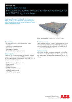


© Copyright 2026