
Welcome to your qMags edition of NASA Tech Briefs!
Welcome to your qMags edition of NASA Tech Briefs! Your electronic issue of NASA Tech Briefs immediately follows this introductory letter. Just use the simple instructions below to learn how to navigate your qMags edition and enjoy its special electronic enhancements. We recommend that you print these two pages so you can refer to them while you are reading the magazine. Or, you can return to these instructions at any time by clicking the ‘first page’ icon on the menu bar, shown below. How to navigate the magazine Take a moment to familiarize yourself with the menu icons at the top of your computer screen. As you move your mouse pointer over each picture, a brief description will appear. Begin by setting your computer to display two pages at a time. (We have pre-set the magazines to be in this configuration, but some readers may need this step). Looking at the Menu Bar at the top of your screen, select VIEW: CONTINUOUS FACING. Next, make sure the width is correct, by selecting VIEW: FIT WIDTH. Now the magazine will fit your screen nicely, although you may want to enlarge or reduce the size of the display as you read. We’ll tell you how to do that, too. ü Turn the page or go back by using the triangle–shaped menu icons at the top of your screen. Alternatively, you can turn the pages forward and back by using the right and left arrows on your keyboard. ü Enlarge the page for easier reading by selecting VIEW: SINGLE PAGE. Use the up and down arrows on the keyboard to scroll through the entire page. You can return to the two-page display by reselecting VIEW: CONTINUOUS FACING. ü Go directly to an article by clicking the title in the table of contents. Click “continued on page…” to follow articles that skip pages. ü Search the magazine electronically by clicking the binocular icon in the menu bar and typing in your subject when prompted. ü Hyperlink to editorial or advertiser websites by clicking when you see a “W” inside the hand shaped cursor, or by clicking on the globe icon shown on the page. All ads have been hyperlinked to advertisers’ websites. Please note that you must be on line to use this feature. Click for Website ABOUT qMAGS.COM qMags.com offers magazine titles from all over the world in our exclusive qMags format. qMags are unique because no other source of online electronic magazines faithfully reproduces 100% of the content found in traditional printed magazines including the design, graphics and advertising that contribute so much to the character and value of a publication. Best of all, qMags.com brings your magazines to life by adding special features that were never possible before in print: ü Audio and video clips transform magazine reading into an exciting multi-media experience. ü Hyper-links to editorial and advertising sites greatly amplify the breadth and depth of readily available information. ü Free, permanent archives of everything you ever buy from Qiosk.com, plus electronic search capability for our entire library of qMags places a powerful new research tool at your fingertips. We hope you enjoy your electronic qMags edition. Be sure to go back to our website to learn more about who we are and what we do. And look for your favorite magazines becoming available in this qMags format soon. LOOKING FOR A FASTER WAY TO ROCKET THROUGH THE PRODUCT-TO-MARKET CYCLE? ACCELERATE WITH IES Rely on IES’s software to accurately model your most complex electromagnetic device or system and predict force, torque, field components, capacitance, inductance, space charge, eddy currents, power system performance and more... Whether you’re designing electric motors, MEMS devices, magnetic sensors, ion guns, high voltage equipment or power electronics systems, Integrated’s innovative electromagnetic simulation software will get you from concept-to-market faster and beats conventional method EM simulation software...hands down. Dream a design, plug it in, optimize it and speed it to market like never before. ● HOW? ● An intuitive graphical user interface designed specifically with the engineer in mind The industry’s most powerful geometric modeler with built-in parametrics for design optimization ● Fully optimized solvers for unequaled speed and performance ● Exact modeling of geometry and superior modeling of regions exterior to device for the most accurate field results ● Advanced, direct plug-In interoperability with leading CAD software ● Unmatched technical support For a test flight of any of IES’s simulation tools, contact Integrated Engineering Software at 204-632-5636, e-mail us at [email protected] or visit www.integratedsoft.com Setting the Standard...Again For Free Info Circle No. 592 or Enter No. 592 at www.nasatech.com/rs May 2002 www.nasatech.com Vol. 26 No. 5 E-Engineering: Defining the Market Composite Materials Absorb Crash Energy Photonics Tech Briefs Why Crawl When You Can Fly? Skip the cocoon of traditional development techniques and fly through your projects with NI LabVIEW 6.1. © Copyright 2002 National Instruments Corporation. All rights reserved. Product and company names listed are trademarks or trade names of their respective companies. ™ Only National Instruments LabVIEW delivers a graphical development environment specifically designed for test and measurement applications. LabVIEW delivers: • Intuitive graphical development, which means no lines of code • Seamless connectivity with thousands of measurement devices • Easy reporting tools so you can communicate across your organization • Instant remote control of your application from any Web browser Soar to the next stage of your development with NI LabVIEW 6.1 – the software that powers measurement and automation. Take your measurements to the web with NI LabVIEW 6.1. ni.com/info If you’re ready to fly, request an evaluation version of LabVIEW by visiting ni.com/info and entering na7z05. For Free Info Circle No. 502 or Enter No. 502 at www.nasatech.com/rs (800) 453-6202 Fax: (512) 683-9300 • [email protected] New From OMEGA! The OMEGA® Made In The USA HandbookTM - Two Volume Set Over 5,000 pages of new and state-of-the-art products Shop online at omega.comsm For Sales and Service - Call OMEGA offers the most impressive customer service in the industry. Fortified with manufacturing knowhow and thousands of products on-hand for immediate delivery, OMEGA is your one-stop choice. s ® DILBERT by Scott Adam w.omega.com ww .com e-mail: info@omega • Same day shipping • Certified calibration lab • Valuable technical articles • Custom design department • Degreed application engineers • Knowledgeable sales associates • Extensive worldwide warehousing • Loaner program with product repair Collection Series To Request Your ® Pack, DILBERT Deck Card Dial: 1-(203 )-329- 1266 Syndicate, Inc. DILBERT © United Feature Get Your Dilbert Card Deck No. 501 Dilbert Decks No. 13 & 14 Available www.omega.com/dilbert Also available on CD ©COPYRIGHT 2002 OMEGA ENGINEERING, INC. ALL RIGHTS RESERVED. Handbook Covers: ©SEPS: Licensed by Curtis Publishing, Indianapolis, IN www.curtispublishing.com Online: usaomega.com Circle Number: 500 NTB Synrad Ad 0502.qxd 04/18/2002 12:02 PM Page 2 ADVERTISEMENT ® CO2 Laser Applications of the Month An Excel Technology Company Creating Contrasting Marks on Polycarbonate with Sealed CO2 Lasers A low-power Synrad CO2 laser was used to create contrasting marks on this polycarbonate part. Sealed CO2 lasers are commonly used for marking text, serial numbers, and bar codes on a wide range of plastics. In many cases, marks are created by engraving into the material. With selected plastics, including polycarbonate, marking at a low laser power creates a color change in the material instead of simply engraving a non-contrasting mark. The typical power range used to mark this material would create a very nice engraved mark, but the lack of contrast may render it difficult to read under some conditions. The easily-readable, contrasting text on the polycarbonate end cap connector shown in the photograph to the left was created at a low power (approximately 10 watts) so that the laser energy creates a "bubble" of bleached material, which contrasts with the surrounding area. The part was marked with a 25watt Synrad CO2 laser and FH-Series Marking Head package. Just 10 watts of power was used at a marking speed of 25” per second. Laser Cutting Carbon Fiber Clean cuts were made on the 0.02"thick woven carbon fiber in the photo to the right with a Synrad Evolution Series 200-watt laser with 5psi air assist. The cuts were made at a speed of 290” per minute in the direction of the weave. The diagonal cut was made at a slightly slower speed, 210” per minute, due to the variation of the material density when cutting in this direction. The durability and light weight of carbon fiber have made it popular in the manufacture of automotive and aircraft parts, sporting equipment, and other industries. In the racing industry, where weight is a crucial factor, metal frames are increasingly being replaced by carbon fiber over urethane foam constructions. This woven carbon fiber was cut using a Synrad Evolution-200 laser. Laser Marking Painted Metal Sealed CO2 lasers are ideal for marking painted or anodized metals. The gun barrel in the photo to the right was marked using a 25-watt Synrad laser, FH-Series marking head, and 200mm lens. With 10 passes of the laser, the metal was marked at a speed of 20 inches per second, cycle time of 4.9s, with a spot size of 0.29mm. The painted surface from the metal is removed during the lasing process, resulting in a contrasting mark. Discover more CO2 laser applications! Sign up for our online Applications Newsletter at www.synrad.com/signup1 A gun barrel marked with a 25watt Synrad CO2 laser. All applications on this page were processed at Synrad’s Applications Laboratory. Synrad, the world’s leading manufacturer of sealed CO2 lasers, offers free process evaluations to companies with qualified applications. Call 1-800-SYNRAD1 for more information. Synrad, Inc. 4600 Campus Place Mukilteo, WA 98275 USA tel 1.425.349.3500 • toll-free 1.800.SYNRAD1 • fax 1.425.349.3667 • e-mail [email protected] • For Free Info Circle No. 504 or Enter No. 504 at www.nasatech.com/rs www.synrad.com NTB Digi-Key Ad 0502.qxd 03/22/2002 4:28 PM Page 1 For Free Info Circle No. 509 or Enter No. 509 at www.nasatech.com/rs NTB Microsoft Ad 0502.qxd 4/6/02 1:19 AM Page 2 EgoÛl`]Ûd]^lÛ`Yf\Û cfgokÛo`YlÛl`]Ûja_`lÛ `Yf\kÛYj]Û\gaf_ ØÚÚDa[jgkg^lÚ:gjhgjYlagfÚ8ddÚja_`lkÚj]k]jn]\ÚDa[jgkg^lÚakÚYÚj]_akl]j]\ÚljY\]eYjcÚg^ÚDa[jgkg^lÚ:gjhgjYlagfÚafÚl`]ÚLfal]\ÚJlYl]kÚYf\£gjÚgl`]jÚ[gmflja]k NTB Microsoft Ad 0502.qxd 4/6/02 1:21 AM Page 3 @fljg\m[af_ÚDa[jgkg^lÚGjgb][lÚJ]jn]jÚÚl`]Úf]o]klÚoYqÚlgÚeYfY_]ÚqgmjÚ]fl]jhjak]Úhjgb][lkÚYlÚ]n]jqÚ gj_YfarYlagfYdÚd]n]dÚ Kg\Yq¿kÚ[gehd]pÚhjgb][lkÚ`Yn]Ú_jgofÚlgÚ]f[gehYkkÚemdlahd]Ú\]hYjle]flkÚgj_YfarYlagfkÚYf\Ú _]g_jYh`a]kÚo`a[`Úe]YfkÚnakaZadalqÚYf\Ú[gddYZgjYlagfÚYj]Úegj]Ú]kk]flaYdÚl`YfÚ]n]jÚGYjlÚg^Úl`]ÚDa[jgkg^l ÙÚE<KÚ ^YeadqÚg^Úk]jn]jkÚDa[jgkg^lÚGjgb][lÚJ]jn]jÚÚogjckÚoal`ÚDa[jgkg^lÚGjgb][lÚGjg^]kkagfYdÚÚlgÚ`]dhÚqgmÚeYfY_]Ú j]kgmj[]kÚYf\Úeg\]dÚhjgb][lkÚY[jgkkÚqgmjÚhgjl^gdagÚN]Z¤ZYk]\ÚY[[]kkÚlgÚhjgb][lÚaf^gjeYlagfÚc]]hkÚ]n]jqgf]ÚafÚl`]Ú dgghÚYlÚYfqÚlae]ÚYf\Ú^jgeÚYfqo`]j]Ú8f\Úl`]Úgh]fÚYj[`al][lmj]ÚafÚDa[jgkg^lÚGjgb][lÚJ]jn]jÚÚYddgokÚqgmÚlgÚ\]hdgqÚ YÚ[mklgear]\Úk][mj]Ú]fl]jhjak]¤k[Yd]Úhjgb][l¤eYfY_]e]flÚkgdmlagfÚl`YlÚafl]_jYl]kÚoal`ÚqgmjÚ[mjj]flÚZmkaf]kkÚ kqkl]ekÚJgÚ]n]fÚo`]fÚl`]j]ÚYj]ÚdglkÚg^Ú`Yf\kÚgfÚl`]ÚbgZÚl`]q¿j]ÚkladdÚg^Úgf]Úeaf\Ú =af\ÚgmlÚ`goÚDa[jgkg^lÚGjgb][lÚJ]jn]jÚÚ[YfÚ`]dhÚqgmÚeYfY_]Úhjgb][lkÚY[jgkkÚ qgmjÚgj_YfarYlagfÚ>gÚlgÛ_ghjgb][lk]jn]j[geÛÛJg^loYj]Û^gjÛl`]Û8_ad]Û9mkaf]kk For Free Info Circle No. 505 or Enter No. 505 at www.nasatech.com/rs NTB Contents 0502 04/17/2002 4:27 PM Page 6 May 2002 • Vol. 26 No. 5 FEATURES 20 Application Briefs 24 NASA Tech Briefs Presents 2001 Product of the Year Awards 27 E-Engineering: Defining the Market 20 SOLUTIONS 6 27 34 Technology Focus: Engineering Materials 34 Composite-Material Structures for Absorbing Crash Energy 36 Improved Conversion Coating for Protection of Metals 36 Chevrel Phases as Potential Thermoelectric Materials 37 Alkyl Pyrocarbonate Electrolyte Additives for Li-Ion Cells 38 Fluorinated Alkyl Carbonates as Cosolvents in Li-Ion Cells 39 Diaminobenzoquinones as Corrosion-Inhibiting Additives 41 Electronic Components and Systems 41 Loss-Tolerant Speech Codec 42 Circuits Control Test Power-Turn-On and –Turn-Off Transients 10 Commercial Technology Team 44 Multiple-Cavity Masers as 32-GHz LNAs 12 UpFront 45 Software 14 Reader Forum 45 Program for Tracking Air-Purification Cartridges 16 Who’s Who at NASA 45 Software for Implementing Fuzzy Logic on Microcontrollers 18 NASA Patents 46 Software for Constructing a Facility-Management Database 22 Technologies of the Month 47 Software Implements Telemetry Protocols 86 Advertisers Index 47 Software for Parallel Processing of Telemetry 50 Software for Global Forecasting of Winds and Waves 50 Software for Modeling Spacecraft Electric Power 52 Mechanics 52 Pressure-Balanced, Low-Hysteresis Finger Seal 56 Instrument for Measuring Extreme Winds 58 Machinery/Automation 58 Mechanized Harvesting of Plants in a Controlled Environment 58 Emergency Landing Using Thrust Control and Shift of Weight 64 Manufacturing 64 High-Velocity, Pulsed Wire Arc Spray 81 DEPARTMENTS NEW FOR DESIGN 81 Products/Software 82 Literature SPECIAL ENGINEERS SUPPLEMENT 1a – 14a Photonics Tech Briefs www.nasatech.com NASA Tech Briefs, May 2002 NTB Algor Ad 03/02.qxd 02/18/2002 3:39 PM Page 1 application of “ Thethis software is universal the only limit is in one’s imagination.” -ALGOR customer Phil Pisczak, Preformed Line Products National HDTV Conversion Effort Requires Re-Engineered Transmission Towers Preformed Line Products (PLP®), a $200 million global leader in the manufacture of cable anchoring systems headquartered in Cleveland, Ohio, is contributing to the national conversion from analog TV to high-definition television (HDTV) with its ROCKETSOCKET™ Dead-end for guy wires, which supports the transmission towers that will be taller, bigger and heavier to bear HDTV's dramatically improved wide screen digital audio/video information. PLP's customer base includes most of the nation's power utility providers and communication providers such as Verizon, Bell South and Adelphia in addition to a variety of resellers. To design the dead-end to support the large communication/broadcast transmission towers that would withstand typical loads including 252,000 pounds of structural weight and wind loading as well as dynamic loads that might result from accidental impact. PLP engineers chose ALGOR to analyze the ROCKET-SOCKET design. PLP used the material austempered ductile iron for increased strength and toughness, rather than ductile iron, which they have used for other dead-end components. The geometry was modeled in PRO/ENGINEER, captured directly in ALGOR and then an impact analysis was performed with ALGOR Mechanical Event Simulation (MES) software. The result was a modification to the geometry of the ROCKET-SOCKET Dead-end to better withstand higher mechanical loadings. By using MES, PLP engineers were able to expedite the testing, reduce the number of iterations in the laboratory and get their product to market more quickly. USA/Canada 1.800.48.ALGOR ALGOR, Inc. 150 Beta Drive Pittsburgh, PA 15238-2932 USA Phone 1.412.967.2700 Fax 1.412.967.2781 France 0.800.918.917 [email protected] challenge.ALGOR.com Singapore 800.120.3775 All trademarks may be trademarks or registered trademarks of their respective owners. For Free Info Circle No. 513 or Visit www.nasatech.com/513 Italy 800.783.132 United Kingdom 0.800.731.0399 NTB Contents 0502 04/17/2002 4:28 PM Page 8 Contents continued 66 Physical Sciences 66 Software for Electromagnetic Detection of Buried Explosives 69 Aircraft Anti-Icing Systems Utilizing Induced Hydrophobicity 70 Characterization of Heat-Flux-Gauge Calibration System 72 Information Sciences 72 Massively Parallel Computation of Electromagnetic Fields 74 Physical Model of Immune-Inspired Computing 75 Mathematical Model of a Quantum Decision Maker 76 IIR Filters for Postprocessing Noisy Test Data 78 Books and Reports 78 Tests of Finger Seals 78 Low-Power, Zero-Vibration Sorption Coolers 78 Inhibited Carrier Transfer in Ensembles of Quantum Dots 78 PRODUCT OF THE MONTH AccuStudy™ time and motion study software from Advanced Time Studies, Bainbridge Island, WA, lets users gather data for single or multiple time studies, then prepares and displays reports and analyses. 12 ON THE COVER Study of Amplification in Optocoupler-Equivalent Circuits The Quadrus EZ™ bar code scanner from Microscan, Renton, WA, enables manufacturers to use 2D symbols to track components through the manufacturing process. It decodes up to 60 codes per second, and is used in the electronics, automation, document handling, automotive, and packaging industries. For more information on the Quadrus EZ and this month’s other new products, see New on the Market on page 81. 79 Area Production in Supercritical, Transitional Mixing Layers (Image courtesy of Microscan) 80 Nanolaminate Mirrors With Integral Figure-Control Actuators 80 Paraffin-Actuated Heat Switch for Mars Surface Applications This document was prepared under the sponsorship of the National Aeronautics and Space Administration. Neither Associated Business Publications Co., Ltd. nor the United States Government nor any person acting on behalf of the United States Government assumes any liability resulting from the use of the information contained in this document, or warrants that such use will be free from privately owned rights. The U.S. Government does not endorse any commercial product, process, or activity identified in this publication. Permissions: Authorization to photocopy items for internal or personal use, or the internal or personal use of specific clients, is granted by Associated Business Publications, provided that the flat fee of $3.00 per copy be paid directly to the Copyright Clearance Center (222 Rose Wood Dr., Danvers, MA 01923). For those organizations that have been granted a photocopy license by CCC, a separate system of payment has been arranged. The fee code for users of the Transactional Reporting Service is: ISSN 0145-319X194 $3.00+ .00 ™ 8 For Free Info Circle No. 576 or Enter No. 576 at www.nasatech.com/rs NASA Tech Briefs, May 2002 ©2002 EDS. EDS and Solid Edge are registered marks and EDS & Design and EDS Solved & Design are trademarks of Electronic Data Systems Corporation or its subsidiaries. With Solid Edge, you design with insight. Just think what Edison could have done with Solid Edge Insight. Intuitive, powerful design tools with built-in knowledge sharing, right out of the box. Solid Edge’s visionary technology adds engineering data extensions to Microsoft document management to ensure first-time fit, cut costs and reduce time-to-market. Solid Edge offers specialized toolsets for your industry. And it’s backed by EDS for support and stability. So get the edge. You’ll electrify your competition. Visit www.solidedge.com or call 877-342-5847. ® ® For Free Info Circle No. 525 or Enter No. 525 at www.nasatech.com/rs NTB TU 0502 04/17/2002 4:37 PM NASA Commercial Technology Team Page 10 NASA’s R&D efforts produce a robust supply of promising technologies with applications in many industries. A key mechanism in identifying commercial applications for this technology is NASA’s national network of commercial technology organizations. The network includes ten NASA field centers, six Regional Technology Transfer Centers (RTTCs), the National Technology Transfer Center (NTTC), business support organizations, and a full tie-in with the Federal Laboratory Consortium (FLC) for Technology Transfer. Call (609) 667-7737 for the FLC coordinator in your area. NASA’s Technology Sources NASA Program Offices If you need further information about new technologies presented in NASA Tech Briefs, request the Technical Support Package (TSP) indicated at the end of the brief. If a TSP is not available, the Commercial Technology Office at the NASA field center that sponsored the research can provide you with additional information and, if applicable, refer you to the innovator(s). These centers are the source of all NASA-developed technology. At NASA Headquarters there are seven major program offices that develop and oversee technology projects of potential interest to industry. The street address for these strategic business units is: NASA Headquarters, 300 E St. SW, Washington, DC 20546. Ames Research Center Selected technological strengths: Information Technology; Biotechnology; Nanotechnology; Aerospace Operations Systems; Rotorcraft; Thermal Protection Systems. Carolina Blake (650) 604-1754 cblake@mail. arc.nasa.gov Dryden Flight Research Center Selected technological strengths: Aerodynamics; Aeronautics Flight Testing; Aeropropulsion; Flight Systems; Thermal Testing; Integrated Systems Test and Validation. Jenny BaerRiedhart (661) 276-3689 jenny.baerriedhart@dfrc. nasa.gov Goddard Space Flight Center Selected technological strengths: Earth and Planetary Science Missions; LIDAR; Cryogenic Systems; Tracking; Telemetry; Remote Sensing; Command. George Alcorn (301) 286-5810 galcorn@gsfc. nasa.gov Jet Propulsion Laboratory Selected technological strengths: Near/Deep-Space Mission Engineering; Microspacecraft; Space Communications; Information Systems; Remote Sensing; Robotics. Merle McKenzie (818) 354-2577 merle.mckenzie@ jpl.nasa.gov Johnson Space Center Selected technological strengths: Artificial Intelligence and Human Computer Interface; Life Sciences; Human Space Flight Operations; Avionics; Sensors; Communications. Charlene E. Gilbert (281) 483-3809 commercialization@ jsc.nasa.gov Kennedy Space Center Selected technological strengths: Fluids and Fluid Systems; Materials Evaluation; Process Engineering; Command, Control and Monitor Systems; Range Systems; Environmental Engineering and Management. Jim Aliberti (321) 867-6224 Jim.Aliberti-1@ ksc.nasa.gov Langley Research Center Selected technological strengths: Aerodynamics; Flight Systems; Materials; Structures; Sensors; Measurements; Information Sciences. Sam Morello (757) 864-6005 s.a.morello@ larc.nasa.gov John H. Glenn Research Center at Lewis Field Selected technological strengths: Aeropropulsion; Communications; Energy Technology; High Temperature Materials Research. Larry Viterna (216) 433-3484 cto@grc. nasa.gov Marshall Space Flight Center Selected technological strengths: Materials; Manufacturing; Nondestructive Evaluation; Biotechnology; Space Propulsion; Controls and Dynamics; Structures; Microgravity Processing. Vernotto McMillan (256) 544-2615 vernotto.mcmillan @msfc.nasa.gov Stennis Space Center Selected technological strengths: Propulsion Systems; Test/Monitoring; Remote Sensing; Nonintrusive Instrumentation. Kirk Sharp (228) 688-1929 kirk.sharp@ ssc.nasa.gov NASA-Sponsored Commercial Technology Organizations These organizations were established to provide rapid access to NASA and other federal R&D and foster collaboration between public and private sector organizations. They also can direct you to the appropriate point of contact within the Federal Laboratory Consortium. To reach the Regional Technology Transfer Center nearest you, call (800) 472-6785. Joseph Allen National Technology Transfer Center (800) 678-6882 Ken Dozier Far-West Technology Transfer Center University of Southern California (213) 743-2353 James P. Dunn Center for Technology Commercialization Westborough, MA (508) 870-0042 Gary Sera Mid-Continent Technology Transfer Center Texas A&M University (409) 845-8762 B. David Bridges Southeast Technology Transfer Center Georgia Institute of Technology (404) 894-6786 Charles Blankenship Technology Commercialization Center Newport News, VA (757) 269-0025 Pierrette Woodford Great Lakes Industrial Technology Transfer Center Battelle Memorial Institute (216) 898-6400 NASA ON-LINE: Go to NASA’s Commercial Technology Network (CTN) on the World Wide Web at http://nctn.hq.nasa.gov to search NASA technology resources, find commercialization opportunities, and learn about NASA’s national network of programs, organizations, and services dedicated to technology transfer and commercialization. Carl Ray Small Business Innovation Research Program (SBIR) & Small Business Technology Transfer Program (STTR) (202) 358-4652 [email protected] Dr. Robert Norwood Office of Commercial Technology (Code RW) (202) 358-2320 [email protected]. nasa.gov Terry Hertz Office of Aero-Space Technology (Code RS) (202) 358-4636 [email protected] Glen Mucklow Office of Space Sciences (Code SM) (202) 358-2235 gmucklow@mail. hq.nasa.gov Roger Crouch Office of Microgravity Science Applications (Code U) (202) 358-0689 [email protected] John Mankins Office of Space Flight (Code MP) (202) 358-4659 jmankins@mail. hq.nasa.gov Granville Paules Office of Mission to Planet Earth (Code Y) (202) 358-0706 [email protected] NASA's Business Facilitators NASA has established several organizations whose objectives are to establish joint sponsored research agreements and incubate small start-up companies with significant business promise. Wayne P. Zeman Lewis Incubator for Technology Cleveland, OH (216) 586-3888 Thomas G. Rainey NASA KSC Business Incubation Center Titusville, FL (407) 383-5200 B. Greg Hinkebein Mississippi Enterprise for Technology Stennis Space Center, MS (800) 746-4699 Joanne W. Randolph BizTech Huntsville, AL (256) 704-6000 Julie Holland NASA Commercialization Center Pomona, CA (909) 869-4477 Bridgette Smalley UH-NASA Technology Commercialization Incubator Houston, TX (713) 743-9155 John Fini Goddard Space Flight Center Incubator Baltimore, MD (410) 327-9150 x1034 Joe Becker Ames Technology Commercialization Center San Jose, CA (408) 557-6700 Marty Kaszubowski Hampton Roads Technology Incubator (Langley Research Center) Hampton, VA (757) 865-2140 Paul Myrda NASA Illinois Commercialization Center West Chicago, IL (630) 845-6510 If you are interested in information, applications, and services relating to satellite and aerial data for Earth resources, contact: Dr. Stan Morain, Earth Analysis Center, (505) 277-3622. 10 www.nasatech.com NASA Tech Briefs, May 2002 ©2002 EDS. EDS and Unigraphics are registered marks and EDS & Design and EDS Solved & Design are trademarks of Electronic Data Systems Corporation or its subsidiaries. NTB EDS Ad 0502.qxd 4/12/02 4:52 PM Page 1 Unigraphics Total Product Engineering. It’s “The Ultimate Megaworks Supercombo.” EDS Unigraphics® delivers Total Product Engineering from concept to reality. Unigraphics is your solution for superior products at lower cost in less time. Now you can automate collaboration by capturing, re-using and sharing knowledge across complex products, easily and transparently. With Unigraphics, the total engineering process is digital, so you can design, simulate, optimize, document, build and test your products in record time. You’ll eat it up. To learn more, call 877-342-5847 or visit eds.com/plm. For Free Info Circle No. 524 or Enter No. 524 at www.nasatech.com/rs NTB UpFront 0502 04/17/2002 4:31 PM Page 12 A dvanced Time Studies, Bainbridge Island, WA, has introduced AccuStudy™, a computer-based time study method that lets users gather data for single or multiple time studies to improve processes. AccuStudy runs on handheld touchscreen computers running ® the Microsoft Windows CE operating system. The software instantly prepares and displays time study results, along with analyses and reports that enable users to pinpoint areas that need attention. The user identifies the icon that represents the process or component being studied, touches it on the screen, and observes it until the next process begins. The software automatically enters appropriate descriptions and value/non-value ratings into the data bank with the observed time. Studies can contain as few as one or as many as 10,000 processes or components. Once data is collected, AccuStudy arranges output into sequential order and lets users create charts, graphs, descriptions, and reports that identify opportunities for greater efficiency. For Free Info Circle No. 711 or Enter No. 711 at www.nasatech.com/rs NASA Introduces “Virtual Iron Bird” A new computer tool under development at NASA’s Ames Research Center in California allows engineers to play “what-if” games with computerized spacecraft and other objects. Using personal computers networked to larger machines, researchers can repeatedly play back chunks of time and study them on a computer monitor, examining details such as views of spacecraft from various angles, temperatures, vibrations, sounds, and data from sensors that computers have recorded. According to project leader Robert Mah of NASA Ames, “If something is broken on a spacecraft, you can troubleshoot the problem ‘virtually’ using new information technologies to do it quicker and more accurately. You can wander through data-enriched 3D models on the computer screen to see how you can fix the spacecraft.” The new tool is called the “virtual iron bird.” Iron bird is an engineering term for a physical model of an aircraft used in part to verify an airplane’s systems. The new tool creates a nonphysical iron bird model within a computer’s memory that engineers can use to analyze past events or test machines before they are built. The computer interface enables recording of pictures, sounds, and statistics such as temperatures, vibrations, and other measurements that could come from a host of sensors or computer programs. The tool works like a “souped-up” CAD/CAM program that can link to databases of 3D models of machines. “You can have engineering teams all over the country and the world,” said Richard Papasin, a project member at Ames. “Without traveling, team members can use the Internet to see how potential changes could affect the object. A second advantage is that developing a virtual model in computer memory costs much less than a real model.” For more information, visit http://link.abpi.net/l.php?20020305A2 . 12 www.nasatech.com Next Month in NTB T he June issue of NTB will include a special feature on the 2001 NASA Commercial and Government Inventions of the Year, awarded each year by NASA’s Inventions and Contributions Board. We’ll also cover the subject of Electronic Design, including the software and hardware used to design and fabricate electronic devices. NASA Tech Briefs, May 2002 NTB Math Works Ad 0502.qxd 4/8/02 10:55 PM Page 1 NEW RELEASE 12.1 AVAILABLE NOW Don’t just predict your real-time system’s performance. Prove it. Simulink® 4.1 Stateflow® 4.1 Real-Time Workshop® 4.1 xPC Target 1.1 Real-Time Workshop Embedded Coder 2 With xPC Target, you can accurately test the performance of real-time embedded control system designs on a costeffective PC long before your final target hardware is available. Simulink code generation products convert block diagrams to real-time New xPC Target products enable real-time rapid prototyping of embedded designs on standard C code for rapid prototyping. You can then x86 PC hardware in any form factor. directly deploy our production quality code to your embedded target. Learn how xPC Target enables rapid prototyping directly on a convenient PC system. To get your Rapid Prototyping Technical Kit, for pricing, or to buy online now, visit www.mathworks.com/ntxp. Design and develop complex embedded systems faster and more efficiently with Simulink products. Visit www.mathworks.com/ntxp or call 508-647-7040 We have a worldwide network of offices and international representatives. Visit our Web site at www.mathworks.com for more information. © 2001 The MathWorks, Inc. For Free Info Circle No. 550 or Enter No. 550 at www.nasatech.com/rs Control System Toolbox 5.1 NTB Reader Forum 0502 04/17/2002 4:39 PM Page 14 Reader Forum Reader Forum is dedicated to the thoughts, concerns, questions, and comments of our readers. If you have a comment, a question regarding a technical problem, or an answer to a previously published question, post your letter to Reader Forum on-line at www.nasatech.com, or send to: Editor, NASA Tech Briefs, 317 Madison Ave., New York, NY 10017; Fax: 212-986-7864. Please include your name, company (if applicable), address, and e-mail address or phone number. W e are involved in the development of an antenna that must be mounted in public roadways, and must sustain motor traffic and weathering. Cars and trucks will be driving over the antenna, and it will be immersed in ice, snow, rain, and slush. The antenna operates in the 800-900 Mhz region and is fed with a foam-filled coaxial cable, probably RG8x. The antenna is a closed cavity design with a ceramic window exposed on the roadway. We would like to have a foam material to fill the antenna cavity in order to preclude the entrance of water and insects. The foam need not have any great physical strength, but it should have a low dielectric constant and loss tangent to minimize de-tuning and loss. The cost of the foaming operation should be minimal and the curing temperatures should be low enough to avoid damage to the feed cable. Thanks for any assistance. John A. Kuecken [email protected] Technologies Wanted Periodically in Reader Forum, we feature abstracts of Demand-Pull Technology Transfer projects. These projects identify technology needs within an industry segment — such as Augmentative Communication — and find solutions to meet those needs. The Rehabilitation Engineering Research Center on Technology Transfer, in partnership with the Rehabilitation Engineering Research Center on Communication Enhancement and the Federal Laboratory Consortium, has developed the Project on Communication Enhancement to identify technologies like those listed below to help persons with communication disabilities who use Augmentative Communication devices. For more details on the project, or to submit technology proposals, visit http://cosmos.buffalo.edu/aac. Input Technologies Input devices provide control of Augmentative and Alternative Communication (AAC) systems. Input devices should use a wireless link to the AAC system. These include speech recognition technology, gesture recognition, and improved eye gaze technology. Speech recognition should be accurate and accommodate users with diverse speech characteristics. Gesture recognition must be non-fatiguing and not dependant on user proximity. Improved eye gaze technology should use discrete eye movement to provide accurate control of the AAC system. It should be self-calibrating, non-fatiguing, and unobtrusive. Driving with confidence Instron's no-compromise technology is deep and flexible, with a product range designed to meet the needs of every budget at every level of manufacturing sophistication. Our instruments test all of the earth's man-made and natural materials. Instron offers tensile, tension, torsion compression, fatigue and impact testing machines as well as structural testing systems. Our software is developed for simple or advanced design standards. Take the high road and standardize on Instron quality, reliability and service. We are the choice for critical applications throughout all industries. You can now own the Instron difference . . . The difference is measurable ▲ 8800 Servohydraulic Testing Systems© ▲ SF 1288 Spring Tester© ▲ Universal Testers© ▲ Rockwell 2000 Tester© ▲ Hand-Held Tester© ▲ Dynatup 9200 Series© Instron Corporation • 100 Royall Street • Canton, MA 02021 • Tel: 800-564-8378 • Fax: 781-575-5751 • Email: [email protected] 14 For Free Info Circle No. 527 or Enter No. 527 at www.nasatech.com/rs NASA Tech Briefs, May 2002 © David Corio “IEEE is a magnet bringing engineers together. Engineering is a language that transcends bureaucracy and nationalism. It gives to us all a common language and understanding.” Ya-Qin Zhang, IEEE Fellow Managing Director, Microsoft Research Asia Build relationships in a worldwide community of innovators. Join IEEE. www.ieee.org/apply For Free Info Circle No. 517 or Enter No. 517 at www.nasatech.com/rs NTB Who's Who 0502 04/17/2002 4:41 PM Extreme sensors High N O N C O N TA C T E D D Y C U R R E N T D I S P L A C E M E N T S E N S O R S Accuracy, Reliability, Structural Integrity 800-552-6267 www.kamansensors.com For Free Info Circle No. 531 or Enter No. 531 at www.nasatech.com/rs Page 18 Who’s Who at NASA Dr. Christopher Dellacorte, Oil-Free Turbo Machinery Technical Leader, Glenn Research Center D r. Christopher Dellacorte is the Oil-Free Turbo Machinery Technical Leader in the Tribology & Surface Science Branch of NASA’s Glenn Research Center in Cleveland, OH. Currently, he is developing new aircraft engines using oil-free turbo engine technology. NASA Tech Briefs: How does oil-free turbine engine technology work and how will it be applied? Dr. Christopher Dellacorte: We are taking the oil out of aircraft engines and gas turbines, and replacing the oil-lubricated ball bearings with air-lubricated ball bearings. Oil has temperature limitations because it burns at a few hundred degrees, but air never burns, so we can run red-hot bearings and significantly reduce the weight. We can also improve the ability to run at very high speeds. NTB: Do you anticipate this becoming mainstream technology? Dellacorte: That’s our intent. What we’re doing now is extending the existing technology to bigger, more powerful systems because the bearing technology itself is an industry-owned technology — there are companies that do these kinds of bearings. Bearings are used in small electrical generators and small compressors for aircraft cabin pressurization and air conditioning so that passengers don’t have to breathe oil that leaks past seals on an airplane. We’ve been using bearings for 30 years but the technology and industry have improved to the point where we think we can use them on a small business jet engine, and that’s the project that we’re currently working on. We expect to run the jet engine in www.nasatech.com about three years and then we’re going to move to bigger jet engines. NTB: Have you already partnered with industry to develop this technology? Dellacorte: On our current business jet engine project we’re partnering with Mohawk Innovative Technology in Albany, NY, and with Williams International in Walled Lake, MI. We anticipate doing a regional jet class engine or supersonic business jet class engine with many of the U.S. engine companies. The government owns a patent on a coating technology that we develop that makes the bearings work at high temperatures. We have two licensees that do the coating technology: Advanced Materials Products in Twinsburg, OH, and Hohman Plating and Manufacturing in Dayton, OH. NTB: Do you envision other applications for this technology? Dellacorte: It could be applicable on microturbines, fuel cell air supply compressors, and turbo chargers. Those are the main applications, in addition to aircraft engines. After 2004, which is when we’re going to demonstrate the first small business jet engine, we are going to get started on bigger engines — what we call regional class engines. The regional jet is a new phenomenon that tries to get people to hop airports that are a few hundred or thousand miles apart. We are working to develop a regional jet engine demonstration project and we hope to demonstrate the first engines in 2007. We’re trying to demonstrate to industry that this technology can work; we’re not trying to build a commercial product. We’re trying to show industry the path so, using their own money, they can then develop commercial versions. A full transcript of this interview appears on-line at www.nasatech.com/whoswho. Dr. Dellacorte can be reached at Christopher. [email protected] NASA Tech Briefs, May 2002 NTB Astromed Ad 11/01.qxd 12/20/01 11:29 PM Page 1 Web Site: www.astro-med.com/de15 For Free Info Circle No. 507 or Enter No. 507 at www.nasatech.com/rs NTB Patents 0502 04/17/2002 4:42 PM World’s Fastest CompactPCI Digitizers Page 16 Over the past three decades, NASA has granted more than 1000 patent licenses in virtually every area of technology. The agency has a portfolio of 3000 patents and pending applications available now for license by businesses and individuals, including these recently patented inventions: Actuator for Flexing a Resilient Covering (U.S. Patent No. 6,312,398) Daniel George Cencer, Johnson Space Center CompactPCI TM 5 GS/s - 8 Bit CompuScope 85GC ➠ 5 GS/s A/D Sampling on two Simultaneous Channels ➠ 500 MHz Bandwidth ➠ 100 Hz Repetitive Acquisition Rate ➠ TV Triggering Capability ➠ Based on Tektronix Technology 16 Bit - 10 MS/s CompuScope 1610C ➠ World’s Fastest 16 Bit Digitizer ➠ 10 MS/s A/D Sampling on two Simultaneous Channels ➠ Differential or Single Ended Inputs ➠ 70 dB Signal to Noise Ratio Compatible with GageScope® World’s Most Powerful Oscilloscope Software Software Development Kits For C/C++, MATLAB and LabVIEW A Tektronix Technology Company 1-800-567-GAGE ext:3405 www.gage-applied.com/ad/nasa502.htm Outside the U.S. contact: Gage Applied, Inc. Tel: +1-514-633-7447 Fax: +1-514-633-0770 e-mail: [email protected] For Free Info Circle No. 403 or Enter No. 403 at www.nasatech.com/rs The power-assisted actuator assembly is designed for flexing restraints in response to movement of an underlying member or controller. The actuator assembly includes a flexible member such as a cord or a fabric panel that has one end coupled to the restraint, and the other end coupled to a drive member such as a drive roller or winch. The drive member, which can be located remotely or locally, pulls on the flexible member to flex the restraint. Coverings and restraints are used to protect underlying members. When that underlying member has a moveable component like a hinged lid or joint, the restraint should move along with the component. For example, body suits and gloves that protect a user from the environment should have restraint layers made to fit closely to the body so that the suit does not prevent or hinder performance of a task. There is a need for an apparatus that reduces the amount of torque required to actuate a restraint layer, such as a glove, that covers a moveable member, such as a hand. This power-assisted joint can include a motion sensor that is coupled to the restraint or is attachable to a human joint and is in electronic communication with the drive member. The assembly is useful in applications including space suit gloves and compliant robot arms. Conducting Compositions of Matter (U.S. Patent No. 6,299,800) Tito Viswanathan, Kennedy Space Center Electrically conducting polymers are of great interest because of potential applications in which they may replace metals and semimetals that require more energy in processing. One of the problems impeding the development of useful polyconjugated conducting materials is their insolubility in the conducting state. Efforts have been made to create novel, water-soluble, conducting polymers, but the need still exists for electrically conducting polymers that have increased processability and solubility. This invention provides a conductive composition of matter comprising linearly conjugated π-systems and sulfonated polyaryl compounds. It also provides a method comprising producing of a fiber or fabric with improved anti-static properties by contacting the fiber with a conductive composition of matter and one or more formaldehyde-based resins; and by curing the fiber or fabric. Portable Hyperbaric Chamber (U.S. Patent No. 6,321,746) William C. Schneider, James P. Locke, and Horacio M. De La Fuente, Johnson Space Center This portable, collapsible hyperbaric chamber and airlock system provides the atmospheric pressures required for standard hyperbaric medical treatments, including both hypobaric and hyperbaric decompression sickness associated with aviation, submarine operations, scuba diving, and space activities. The device can be sized to contain at least one patient and one attendant, and can be stored flat with minimal volume. Conventional chambers made of solid metal are heavy and not portable. The new chamber is constructed with a toroidal inflatable skeleton that supports the structure, allowing the attendant and/or patient to enter. Oval hatches mate against bulkhead rings, and the chamber is pressurized. The hyperbaric chamber has an airlock that allows the attendant to enter and exit the patient chamber during treatment. Visual communication is provided through portholes in the patient and/or airlock chamber. Life monitoring and support systems are in communication with the inside of the chamber via conduits and/or sealed feed-through connectors. The chamber can be stowed in the storage area of a room, ship, spacecraft, or other area where space is limited. When deflated, the chamber collapses into a small shape. For more information on the inventions described here, contact the appropriate NASA Field Center’s Commercial Technology Office. See page 10 for a list of office contacts. www.nasatech.com NASA Tech Briefs, May 2002 NTB VX Ad 0402.qxd 03/13/2002 11:20 AM Page 1 In the world of CAD/CAM, we're changing the rules. VX OverdriveTM. Premium-performance CAD/CAM that's fun to drive. Design through manufacturing with no stops VX® blows the doors off of CAD/CAM with a value-priced, designthrough-manufacturing system so superior it leaves everything else in the dust. New VX Overdrive is so feature-rich, so fun to drive, what used to be roadblocks at every phase now become thrilling curves you can negotiate with ease. So easy to use VX Overdrive is loaded with flexibility to help you fly through even the toughest jobs. Unique surface creation tools let you blast through challenges at high speed. And its full integration from design through manufacturing means engineers can bring projects to market faster using a single, seamless system. With VX Overdrive, if you can imagine it, you can build it. your buck of any system, plus the ability to import legacy data and the highest level of interoperability on the market (STEP, IGES and direct CAD translators). Take a test spin See for yourself how VX Overdrive is changing the rules. Contact us for a demo today. Premium performance without the premium price VX Overdrive comes fully loaded so you’ll get the most bang for VX.COM 321-676-3222 ©2001, VX Corporation. VX Overdrive and the VX logo are trademarks of VX Corporation. For Free Info Circle No. 539 or Enter No. 539 at www.nasatech.com/rs NTB ApplBriefs 0502 04/18/2002 11:07 AM Page 20 plication Briefs Application Briefs Applicat Application Briefs Application Briefs Appli p p l i Application c a t i o n B rBriefs i e f s Applicat plication ABriefs Application Briefs Application Briefs Appli Imaging Technology Upgrade plication Briefs Application Briefs Applicat Improves Hubble Space Telescope Application Briefs Application Briefs Appli Charge-coupled device (CCD) technology Scientific Imaging Technologies, Inc. (SITe) Tigard, OR plication Briefs Application Briefs Applicat (503) 431-7199 www.site-inc.com Application Briefs Application Briefs Appli plication Briefs Application Briefs Applicat Application Briefs Application Briefs Appli plication Briefs Application Briefs Applicat Application Briefs Application Briefs Appli plication Briefs Application Briefs Applicat Application Briefs Application Briefs Appli plication Briefs Application Briefs Applicat Application Briefs Application Briefs Appli plication Briefs Application Briefs Applicat Application Briefs Application Briefs Appli plication Briefs Application Briefs Applicat Application Briefs Application Briefs Appli plication Briefs Application Briefs Applicat Application Briefs Application Briefs Appli plication Briefs Application Briefs Applicat Application Briefs Application Briefs Appli plication Briefs Application Briefs Applicat Application Briefs Application Briefs Appli plication Briefs Application Briefs Applicat Application Briefs Application Briefs Appli Launched in orbit in April 1990, the Hubble Space Telescope has provided astronomers and other researchers with reams of data and spectacular images of celestial bodies. In March, the Space Shuttle Columbia began an 11-day mission to upgrade several systems on the Hubble Space Telescope, including installation of an Advanced Camera for Surveys (ACS), which utilizes imaging technology developed by Scientific Imaging Technologies, Inc. (SITe). The SITe sensor was chosen to replace one of the company’s earlier imagers that has operated on the Hubble since its refurbishment in 1997. This technology is enabled by the use of charge-coupled devices (CCDs), which replace vacuum tube-based imagers and film used in conventional cameras. Combined with optics, a cooling system, and operating electronics, these microchips produce high-resolution images by turning light into a stream of electronic signals, which can be recorded and displayed on a computer or television screen. By using CCD technology, it is estimated that the Hubble’s imaging system will be 10 times more powerful than its current system. SITe’s CCD technology incorporates a proprietary process for thinning and strengthening the substrate to accommodate back-illumination of the pixels, a process that yields devices with high quantum efficiency (QE) over a range of wavelengths from near-infrared to ultraviolet. QE — or light-detection efficiency — measures the percentage of incident photons a CCD can detect. When configured with an anti-reflective coating, a thinned, back-illuminated CCD can deliver QE in excess of 90 percent. When the photon falls on the CCD, it is absorbed and generates an electron. These electrons are collected in the “bucket” nearest the point where the photon was absorbed. The number of electrons collected in a pixel depends upon how many photons fall on that pixel. After the camera shutter closes, the number of electrons in each pixel are measured and a voltage proportionate to that number is generated. That voltage can be amplified, digitized, stored, and displayed. SITe’s Wide Field Channel (WFC), one of three imaging channels comprising the Advanced Camera for Surveys (ACS). The ACS will replace the Faint Object Camera, the last of the original cluster of axial instruments on the Hubble. The threemeter-long ACS contains three imaging channels, two of which utilize SITe technology. The Wide Field Channel contains two SITe 2K × 4K chips that form a 4K × 4K mosaic; and the High Resolution Channel uses a single 1K × 1K SITe device. The new technology will enable the Hubble to see farther, more clearly, and in greater detail than ever before. The ACS will double Hubble’s field of view and enhance its image quality. The new camera will be used to map the distribution of dark matter, detect the most distant objects in the universe, and search for planets and galaxies. 20 After its initial refurbishment in 1997, the Hubble obtained this image of Mars, the sharpest view of the Red Planet ever taken from Earth. In 1997, SITe’s technology deployed on the Hubble was applied to an early-detection breast biopsy system currently used in hospitals worldwide. SITe CCDs also are used in protein crystallography and in the development of new drugs and therapies. Other application areas include manufacturing quality control, environmental monitoring, and security inspection and surveillance. www.nasatech.com For Free Info Circle No. 710 or Enter No. 710 at www.nasatech.com/rs NASA Tech Briefs, May 2002 NTB Dewetron Ad 02/02.web 02/21/2002 9:50 AM Page 2 For Free Info Circle No. 544 or Enter No. 544 at www.nasatech.com/rs NTB Tech of the Month 0502 04/18/2002 11:10 AM Page 22 Technologies of the Month Sponsored by For more information on these and other new, licensable inventions, visit www.nasatech.com/techsearch Using Conductance/Capacitance to Measure Fuel Mixture Ratios Water-Wash Paint Overspray Solution Reduces or Eliminates Paint Waste Thilo Schwoebel, Robert Bosch GmbH, Germany Caterpillar A fuel sensor technology uses the fuel itself to form the dielectric of a capacitor enabling fuel mixture ratio to be maintained. The sensor can be assembled using ceramic-molded components and materials developed for thick-film technology. The measuring cell is composed of a cavity formed by ceramic carriers. The fuel mixture flows through the cavity and becomes part of the evaluation circuit. The measuring cell can include a second cavity that is closed and contains a reference medium. The capacitors are part of the evaluation circuit that notes any capacitance changes as the conductance of the fuel mixture changes. The sensor is suitable for internal combustion engine applications, including electrical generators, automobiles, aircraft, and liquid-fueled rockets. Get the complete report on this technology at: www.nasatech.com/techsearch/tow/schwoebel.html Email: [email protected] Phone: 617-557-3837 Overspray of protective coatings may cost manufacturers half or more of their purchased paint. The majority of today’s waterwash paint lines use forced air to direct “live” airborne droplets of paint through a cascading water curtain just prior to advancing to the system’s exhaust stacks. An alternative to this method uses hydrophobic fumed silica (HFS) particles in conjunction with the water-wash system design that do not mix with water. HFS particles require no technical labor for chemical titrations, booth water, or additives. When droplets of “live” paint are introduced to the HFS-treated water-wash booth, the HFS particles rapidly encapsulate the droplets by physical phenomena and result in non-tacky HFS-paint agglomerations that can be manually removed. It is possible to process HFS detackified paint “sludge” and re-use it in paint or other products utilizing similar chemistry. The detackification and recovery technology has proven applicable to all solvent-based paints on which it has been tested, including automotive and construction equipment. Get the complete report on this technology at: www.nasatech.com/techsearch/tow/caterpillarHFS.html Email: [email protected] Phone: 617-557-3837 Phosgene Catalyst Reduces Toxic By-Product DuPont The process used to manufacture phosgene, a key ingredient in the production of polyurethane and polycarbonate resins, also creates carbon tetrachloride (CCl4), an ozone-depleting substance. Federal and state environmental guidelines require that CCl4 be removed from the product stream to prevent environmental contamination. If it cannot be controlled at the source during production, expensive “end-of-the-pipe” equipment has to be installed and maintained by the manufacturers. Researchers at DuPont have developed a phosgene catalyst that reduces emission of CCl4 by more than 80%. It was discovered that chlorine, one of the ingredients used to make phosgene, reacted with the granulated carbon catalyst to produce high levels of CCl4. To repair this, a replacement catalyst was utilized that can be applied to commercial pressurized tube bundle reactors. Benefits include a reduction of process downtime because the new catalyst does not deplete as rapidly as the former. Get the complete report on this technology at: www.nasatech.com/techsearch/tow/dupont-phosgene.html Email: [email protected] Phone: 617-557-3837 22 Communication Software Securely Bridges Diverse Firewalls Science Applications International Corporation Firewall transit communication has been limited to participants on opposite sides of single firewalls, and there has been no “off-the-shelf” technology offering seamless and secure cross-firewall communication. An application called SD-Link features an Internet-based intermediate server that maintains connections and exchanges data between clients behind separate firewalls. SD-Link permits worldwide communication across multiple private and public networks while maintaining security through end-to-end encryption and authentication. The application can communicate either directly to an SD-Link communication component at any seat of a standalone network, or through an SD-Link-enabled applet for browserbased operation. Get the complete report on this technology at: www.nasatech.com/techsearch/tow/saic.html Email: [email protected] Phone: 617-557-3837 www.nasatech.com NASA Tech Briefs, May 2002 NTB Compaq Ad 0502.qxd 4/18/02 4:17 PM Page 2 TEAM POWER Designed for high performance and reliability. Tested and proven by leading CAD-ISV partners, a Compaq Evo™ Workstation with the latest Intel® Xeon® Processor simply makes things happen. These powerful Windows® platform machines will give your engineers some concurrent quality time. Now fully functional prototypes, more efficient 3D design, and Webbased project management and collaboration stand at-the-ready. For CAD solutions, put a Compaq Evo Workstation on your team. It will be high fives all around. Compaq CarePaq Services provides a variety of upgrades to enhance the base warranty on your Compaq products. [ to equip your team for victory visit compaq.com/workstations or call 1-800-888-0414 The Power of MACROPROCESSING Compaq PCs use genuine Microsoft® Windows® www.microsoft.com/piracy/howtotell Compaq, the Compaq logo, Evo and Inspiration Technology are trademarks of Compaq Information Technologies, L.P. in the U.S. and other countries. Intel, the Intel Inside logo, and Xeon are trademarks or registered trademarks of Intel Corporation or its subsidiaries in the United States and other countries. Other products mentioned herein may be trademarks of their respective companies. Compaq is not liable for editorial, pictorial, or typographical errors in this advertisement. © 2002 Compaq Information Technologies, L.P. For Free Info Circle No. 591 or Enter No. 591 at www.nasatech.com/rs NTB Prod./Year Coverage 0502 04/18/2002 11:12 AM Page 24 NASA Tech Briefs Presents 2001 Product of the Year Awards T he seventh annual NASA Tech Briefs Readers’ Choice Product of the Year Awards were presented March 18 at a special reception at the John Hancock Center in Chicago, in conjunction with the kickoff of the National Manufacturing Week show. The awards, chosen by the more than 195,000 readers of NASA Tech Briefs, recognized the Gold, Silver, and Bronze winners, as well as nine Product of the Year Finalists. Each month, the editors of NASA Tech Briefs choose a Product of the Month, a product that exhibits exceptional technical merit and practical value to our Product of the Year Finalists from Dolch Computer Sysreaders. All 12 products are placed on a tems join NASA Tech Briefs’ editor and associate publisher, Linda Bell. From left: Michael Kadri, vice presiballot and readers vote for the most indent and general manager for Dolch’s Canadian offices; VX Corporation’s vice president of novative product introduced to the Jim Ciardella, president of Dolch; and Tom Brassil, vice sales & marketing, Bob Fischer, acengineering community during the president of sales and marketing. cepts the 2001 Gold Award for Prodyear. The product receiving the most uct of the Year. votes is named the Gold Winner and Product of the Year. The following companies The 2001 Gold Award for Product of the Year was presented to were honored as Product VX Corporation of Palm Bay, FL, of the Year Finalists for its VX CAD/CAM Version 5 for 2001: software. The top prize was accepted by Bob Fischer, vice presi• Dolch Computer Systems (Fremont, dent of sales & marketing for VX, CA) for the FlexPAC ™ rugged portable computer (www.dolch.com) who commented that “The readers of NASA Tech Briefs are among • ifm efector (Exton, PA) for the OJ the most technically sophistiSeries photoelectric sensors (www.ifmefector.com) cated and influential people in the engineering world. This • iOtech (Cleveland, OH) for the recognition is incredibly gratify- 2001 Product of the Year Award Winners: (From left) DaqBoard/2000c™ data acquisition boards (www.iotech.com) ing and really underscores how Bronze Award recipient Ray Almgren of National Instruments; Bob Fischer of VX Corp., Gold Winner; and our approach to CAD/CAM NTB associate editor, Laura Raduta, accepting for Silver • Mountz (San Jose, CA) for the Wizard solves difficult design and manu- Winner, MathSoft Engineering & Education. torque & force analyzer module for PDAs (www.etorque.com) facturing problems for the most tent across and throughout an organiexacting users.” • OMEGA Engineering (Stamford, CT) zation. It provides a tool for sharing Version 5 of VX CAD/CAM — last for the OM DL-Series portable dataloggers (www.omega.com) math on the Internet, as well as via August’s Product of the Month — is a corporate extranets and intranets. design-through-manufacturing pack• think3 (Santa Clara, CA) for (www.mathsoft.com) age that integrates product design and thinkdesign 6.0 CAD software (www.think3.com) National Instruments of Austin, TX, manufacturing to eliminate the gap betook home the Bronze Award for Meatween CAD and CAM packages. Ver• Vistagy (Waltham, MA) for EnCapta™ surement Studio™ 6.0, a set of measuresion 6 of the software was introduced at collaborative engineering software (www.vistagy.com) ment tools that engineers can use to National Manufacturing Week and is create test, measurement, and control now available (www.vx.com). • Wavetek Meterman Test Tools applications in various programming The Silver Award was won by Math(Everett, WA) for Meterman test & measurement instruments languages. Ray Almgren, vice president Soft Engineering & Education of Cam(www.metermantesttools.com) of product strategy for National Instrubridge, MA, for Mathcad® Client collaborative math software. The award ments, accepted the award. Measure• Wolfram Research (Champaign, IL) for was accepted by Laura Raduta, Associment Studio lets users display data on CalculationCenter technical calculation software (www.wolfram.com) ate Editor of NASA Tech Briefs. Last Ocreal-time 3D or 2D graphs and charts tober’s Product of the Month, Mathcad that can be annotated to explain sig(All photos by Michael J. Kardas, Kardas Client was designed for sharing and nificant dips or spikes in the data. Photography, Chicago, IL) collaborating on Mathcad-created con(www.ni.com) 24 www.nasatech.com NASA Tech Briefs, May 2002 FEMLAB F EMLAB –Multiphysics multiphysics in M ATLAB ® V I S I T W W W. C O M S O L . C O M F O R I N T E R A C T I V E D E M O S A N D T U TO R I A L S ATLAB FEMLAB supplies highly sought-after new ® technology for the modeling and simulation of physics in all science and engineering fields. Its main attribute is the ease with which modeling can be performed and its unlimited multiphysics capabilities, in 1D, 2D and 3D — the perfect way to apply state-of-the-art numerical analysis to your expertise in modeling. FEMLAB i s a re g i s t e re d t r a d e m a r k o f C O M S O L A B . M AT L A B ® Order your free literature kit! ® Visit www.comsol.com/ient or call +1-781-273-3322 i s a reg i s t e red t r a d e m a r k o f T h e M a t h Wo r k s , I n c FEMLAB ® VISIT WWW.COMSOL.COM FOR INTERACTIVE DEMOS AND TUTORIALS VISIT WWW.COMSOL.COM FOR INTERACTIVE DEMOS AND TUTORIALS FEMLAB is a registered trademark of COMSOL AB. – multiphysics in MATLAB ® ® FEMLAB supplies highly sought-after new technology for the modeling and simulation of physics in all science and engineering fields. Its main attribute is the ease with which modeling can be performed and its unlimited multiphysics capabilities, in 1D, 2D and 3D — the perfect way to apply state-of-the-art numerical analysis to your expertise in modeling. Microwave propagation in a T-shaped waveguide. The distribution of the energy between the two legs is controlled by a post at the waveguide wall. An S-parameter analysis is done in a MATLAB script. Oxygen concentration in the cathode of a fuel cell (PEMFC) and its implications on current distribution. Model of a stirred tank reactor solved with Navier-Stokes equations. The image shows velocity field flow lines and pressure distribution on the face of the stirrer. F E M L A B K E Y F E AT U R E S Flexible and powerful graphical user interface Automatic mesh generation, adaptive mesh and multigrid Powerful solvers for linear, nonlinear and time-dependent systems of partial differential equations (PDE s) Extensive postprocessing capabilities Model Libraries with over fifty models fully documented from various engineering fields Ready-to-use application modes for different engineering fields Equation-based modeling for arbitrary systems of PDE s F E M LA B P U T S YO U IN THE FRONTLINE FEMLAB employs sophisticated numerical techniques developed by our staff of leading scientists in collaboration with industry experts from around the world. These professionals had a goal of making modeling available to every engineer and scientist. FEMLAB is the result of our commitment to putting engineering mathematics in a box. Order your free literature kit! Visit www.comsol.com/ient or call +1-781-273-3322 w w w. c o m s o l . c o m FEMLAB is a registered trademark of C O M S O L A B . M AT L A B is a registered trademark of The MathWorks, Inc VISIT WWW.COMSOL.COM FOR INTERACTIVE DEMOS AND TUTORIALS Built-in user-friendly CAD tool for solid modeling in 1D, 2D and 3D This square-shaped spiral inductor is used for bandpass filters in micro electromechanical systems (MEMS). The FEMLAB simulation takes the nonuniform current density in the coils into account to compute an accurate magnetic flux arround the coils. The inductance of this inductor is 2.1 nH, which is obtained by integrating the magnetic energy. Using the programming language of FEMLAB for parametric analysis, you can find the correlation between the induction and the input parameters of the model. F E M L A B K E Y F E AT U R E S Flexible and powerful graphical user interface Built-in user-friendly CAD tool for solid modeling in 1D, 2D and 3D Automatic mesh generation, adaptive mesh and multigrid Powerful solvers for linear, nonlinear and time-dependent systems of partial differential equations (PDE s) Extensive postprocessing capabilities Model Libraries with over fifty models fully documented from various engineering fields Ready-to-use application modes for different engineering fields Equation-based modeling for arbitrary systems of PDEs F E M L A B P U T S YO U IN THE FRONTLINE employs sophisticated numerical techniques developed by our staff of leading scientists in collaboration with industry experts from around the world. These professionals had a goal of making modeling available to every engineer and scientist. FEMLAB is the result of our commitment to putting engineering mathematics in a box. FEMLAB In the design of electrodes for water electrolysis, it is important to minimize the voltage losses at a given total current. FEMLAB modeling helps the engineer in the design of the electrode geometry and the current collector. The model gives the current density distribution and the potential distribution in the system. These results make it possible to avoid excessive degradation of the active electrode surface and overheating of the welds at the position of the current collector. When designing an electric motor it is important to design the rotor shaft so that no eigenfrequencies exist in the working range of the rotational speed. It is also important to study the shape of the eigenmode and not just the eigenfrequencies. In the eigenfrequency analysis, one end of the shaft is fixed and the other end is free to rotate and axially deform. The image shows deformation and rotation angle in the second eigenmode, using different visualization options like colormaps and scaling. Order your free literature kit! Visit www.comsol.com/ient or call +1-781-273-3322 F E M L A B i s a re g i s t e re d t r a d e m a r k o f C O M S O L A B. w w w. c o m s o l . c o m V I S I T W W W. C O M S O L . C O M F O R I N T E R A C T I V E D E M O S A N D T U TO R I A L S The most common reactor for environmental protection, which we encounter or use everyday, is the catalytic converter in automobiles. In these monolithic catalysts, carbon monoxide and nitrous oxides are converted into relatively harmless species like carbon dioxide and nitrogen. To optimize the utilization of the expensive catalyst, it is important to be able to model the reactor at different operational conditions. In this FEMLAB model, mass and heat balances are coupled to compute temperature distribution and flowlines in the reactor. NTB Feature 0502 04/18/2002 11:20 AM Page 27 E-Engineering: Defining the Market he notion of actually doing engineering on-line or via the Internet is just starting to take hold,” according to Jim Schultz, director of e-business and additional sales channels for MSC Software. So as this idea of collaborative engineering, or e-engineering, continues to become a more clearly defined market, vendors are struggling to differentiate themselves, and users are struggling through the maze of available products. With all of the product lifecycle management (PLM), viewing, meeting, and other Internet-based engineering tools out there, what’s really working? What products are manufacturers using in a practical way today? “We recognize that there’s a new way of designing, developing, and manufacturing products,” said Mike Grandinetti, senior vice president and chief marketing officer for PTC’s Windchill Business Unit. “The old way was that everybody worked in the same building and could walk down the hall to talk to their colleagues. The world doesn’t work that way anymore. Engineering has always culation software. “Some vendors feel that the correct way to approach Internet-based collaboration is to come up with Web-based extractions of specific design elements within a tool. Their technology becomes the way that the extraction is communicated from tool to tool,” Tung added. “That almost never succeeds.” Providing engineers with such tools at their fingertips is where the evolution begins, said Schultz. “This will be facilitated by improvements to the Web itself, including the employment of smart agents. We want to create more Web-enabled access to tools, provide consultant services, and take these complicated tools and make them more userfriendly.” User-friendly is not a term generally equated with Internet-based engineering tools. That’s part of the reason why only the most basic of collaborative products are being used today, according to Greg Milliken, vice president of marketing for Alibre, maker of Alibre Design, a data sharing, CAD, and realtime collaboration system. “Generally, only very simple virtual meetings and some very limited client-server data access or visualization is being used to any significant extent today,” Milliken said. “The biggest thing used is probably just e-mail — sending drawings or documents back and forth to be reviewed and then sent back. In the next five years,” he continued, “individuals will be empowered to connect and share data with anyone they 3D TeamWorks from SolidWorks is an on-line environment want, since the tools will be so where users can conduct real-time design reviews and coor- inexpensive, everyone will dinate team activities. have them.” E-mail as a manufacturer’s been a team sport, but companies really only collaboration tool just won’t cut it, haven’t given their engineering and said Chris Will, marketing director of manufacturing people the tools to colcollaboration products for EDS PLM Solaborate,” Grandinetti added. lutions. “Engineers spend over 75% of “Where I don’t see a lot of success their day trying to find the right inforamong the e-engineering based prodmation,” he said. “When you think about ucts is where they try to tie together disthe complexity of these distributed colparate disciplines,” said Jim Tung, chief laborative teams, and trying to synchromarket development officer for The nize to make sure everybody’s working MathWorks, a supplier of technical calthe right sets of information, it’s a major “ T NASA Tech Briefs, May 2002 www.nasatech.com challenge to do without a collaboration tool. If I’m e-mailing files, how do I know everybody’s designing to the right information? Do they have to translate to some other format or CAD system?” SolidWorks’ product manager for collaboration products, Robert McDonald, said that his research with the SolidWorks customer base as far as what collaborative products they’re currently using was very surprising. “We assumed Algor, Inc.’s Webcasting audio/video technology for distance learning and free, live software demonstrations enable education and customer support over the Internet. our customer base knew as much as we do. But they have not even heard of simple things like WebEx to do collaboration. This space is so new that they’re looking to their CAD vendor to be able to provide a solution they can understand.” SolidWorks’ latest offering in the collaboration space is 3D TeamWorks, a Web-based service through which design teams can review designs, share information, and troubleshoot problems. Despite the fact that e-mail today seems like a “stone-age” tool, the traditional methods of communication, such as faxes, phone calls, web conferencing, and yes, e-mail, are still the most-used forms of collaboration. More generic collaboration tools like document-sharing products are at a 50% adoption rate, according to Grandinetti. “We’re on the 27 PLM we know they know CAT IA CATIA: driving innovation, this advanced 3D design a links design and manufacturing, improves collaboration Along with IBM’s industry expertise, it’s part of a compl business we know they know IBM and the e-business logo are trademarks or registered trademarks of International Business Machines Corporation in the U.S., other countries or both. CATIA is a registered trademark of Dassault Systemes S.A. ©2001 IBM Corporation. All rights reserved. Collaboration Innovation CATIA: driving innovation, this advanced 3D design and engineering software from Dassault Systemes links design and manufacturing, improves collaboration, reduces costs and gets products to market faster. Along with IBM’s industry expertise, it’s part of a complete PLM solution. See it at ibm.com/solutions/catia business solutions CATIA and Innovation CATIA,® the world’s leading CAD/CAM/CAE software, takes 3D design and innovation to a new level. It streamlines the entire development process from idea to design and through the entire product life cycle by providing a virtual environment for testing, prototyping and manufacturing. It drives the development of innovative, high-quality products, while drastically reducing time for development, cutting costs and providing a faster return on investment. Better still, it opens up a new range of market opportunities by offering not only the ability to customize on a massive scale, but also personalization for every customer. In short, it gives you the power to create innovative products in a market where innovators lead. And ultimately win. PLM and Collaboration IBM’s Product Lifecycle Management (PLM) solutions provide an integrated approach to the development of products that fosters innovation. How? By linking your product team’s knowledge and processes with the network of suppliers, engineers, customers and partners on which your success ultimately depends. CATIA is an integral part of IBM’s PLM solutions. See for yourself The trial code CD version of the latest, awardwinning CATIA software is yours to try, free, for 30 days. Simply call 1 800 IBM 7777 ( Priority Code 6N1FS030) or visit our Website: ibm.com/solutions/catia NTB Feature 0502 04/18/2002 11:21 AM Page 29 cusp of true collaborative engineering think it’s just the same old thing with a Internet, and as that happens, you’ll being commonplace,” he said. “We’re different name.” start to see additional types of engineermaking the technology much more acAlibre believes that the broad cateing activities or other software usage becessible to everyone.” gories of PLM or collaborative product coming more prevalent. There are perBut does accessibility equal widecommerce (CPC) are too spread use? “The grass-roots tools that vague, Milliken explained. The are useful to one engineer, and then CPC space, however, is exactly to groups of engineers, have a better where companies like chance of taking hold,” predicted Web4/netGuru have made Allen Razdow, senior vice president of their home. Their e-Review strategic planning for Mathproduct is a Web-based, realSoft Engineering & Educatime collaboration tool for doction, which has added PDM ument review and markup that functionality on top of its supports more than 150 file forMathcad software. “Access to mats natively. the Internet tends to be more “We’ve got people that will tightly controlled in engineerdesign on a particular platform, ing environments,” he added. and they’ll use a collaborative “The dot-com model of getengine to share that informating on the Web and downtion,” said Ben Parikh, director loading your favorite tool of corporate sales and marketdoesn’t work well in more ing for Web4. “In the future, controlled industries where we’ll probably have real-time inIn this image from Spicer’s ViewCafe viewing tool, a cross-sectioned 3D the network has to be care- model is shown in the ViewCafe applet. The window behind shows the teractive design on-line without fully managed and accessed.” same model in 2D-projection mode with markups. having to go back to your deskThere is a category of top and make changes.” products that work, according to Robert A relatively new entry into the viewer formance issues now, and most of them Kross, vice president of Autodesk’s Mancategory is Spicer Corp., which introare tied to the fact that the Internet itself ufacturing Division. Those are asynchroduced ViewCafe™ 2.1. The Java-based needs to be expanded,” he added. tool lets engineers conduct document nous tools. “There are a lot of synchro“We’re planning to provide software in view, markup, and collaborative review nous tools out there, but they require real time over the Internet through a sessions for over 150 file formats, includboth parties to be on the Internet at the browser, so instead of purchasing the ing CAD, Microsoft Word and Excel, same time, working together. That’s not software, you’re leasing it to get a speraster, vector, and PDF, through a Web the way people work today, especially in cific application done.” browser. different time zones,” Kross said. “The customers who are driving col“The Internet is still used primarily laboration are driving it from a for information exchange,” explained product standpoint,” said Bob Williams, product manager for Michael Wheeler, vice president ALGOR, Inc., supplier of finite element and general manager of the meanalysis and mechanical event simulachanical business unit for tion software. “Among other things, we ANSYS, which supplies simulautilize the Internet to offer distance tion software. “Our products are learning through Webcasting technolbecoming more Web-enabled ogy; live, Internet-based product due to customer demand. Peodemonstrations; and automatic generaple are overcoming their fears of tion and publishing of HTML reports to transmitting company data over the Internet that include Web-based the Internet,” Wheeler added. graphics and animations.” The Internet began — and Many organizations don’t want to continues to be — a communishare their data during the design cation device that lends itself phase, said George Schildge, vice presiwell to collaborative engineerdent of corporate communications for ing. But before that can be comCoCreate, which supplies the OneSpace monplace, many changes need suite of collaborative product developto take place, including distinment tools. “Collaboration is about guishing what products are out Solid Edge Insight Technology from EDS enables viewing and rotating of the most current 3D model without engiteamwork and sharing ideas, but many there and how they’re different. neering experience. Part properties, a Bill of Materials, and instant messaging also are available. organizations are working in the oldProducts, Products school model of ‘I’ll create it and when Everywhere Proficiency offers its Collaboration I’m done, I’ll throw it over the fence to Are collaborative engineering prodGateway that enables manufacturers to manufacturing and let the engineers ucts still too vague and confusing for share product design information, even deal with it.’” many manufacturers to understand? Yes, if it was created using different mechanPart of the evolution of Internet-based said Alibre’s Milliken. “Most of the largeical design products. It lets users of four engineering tools will occur as the Interscale expensive and complicated entermechanical CAD systems — Dassault Sysnet itself continues to evolve. Said prise systems are not being used in a big temes’ CATIA, PTC’s Pro/ENGINEER, Williams, “There are ongoing efforts to way — they have yet to be proven. Many continually improve the backbone of the (Continued on pg. 32) NASA Tech Briefs, May 2002 www.nasatech.com 29 NTB MSC Ad (Spread) 0502.qxd 4/11/02 4:56 PM Page 2 NTB MSC Ad (Spread) 0502.qxd 4/11/02 4:57 PM Page 3 For Free Info Circle No. XXX or Enter No. XXX at www.nasatech.com/rs For Free Info Circle No. 526 or Enter No. 526 at www.nasatech.com/rs NTB Feature 0502 04/18/2002 11:22 AM Page 32 and EDS’s Unigraphics and I-DEAS — exchange digital assembly or part models without having to learn another tool or lose data. Another product category tossed into the mix is the ASP (Application Service Provider) model. ANSYS’s collaborative product offering, eCAE, is similar to an ture is worth a thousand words,” exmaking a large number of design plained PTC’s Grandinetti. “It provides changes,” said ALGOR’s Williams. “So, comfort and security to the manufacturwe have made our FEA models and reing buyer.” sults directly associated with their CAD Williams believes that ALGOR’s users data so the user can more easily manage already understand the values and prinupdates to the geometry and analysis ciples behind these tools, but they need data related to their designs.” to incorporate the ones that work best. CAD companies like EDS are provid“It sounds simple,” he said, “But it comes ing their own collaboration tools down to the individual company. In the that tie into their core CAD prodend, it’s the user who will tell you what uct — or another CAD product. they need to be effective. Chris Will explained that Team“A small machine shop with four engiCenter Engineering lets users neers probably would find it not to be manage other related informacost-effective to have a PDM application tion besides CAD data, and prothat forces them to use a specific CAD vides a configured design, intepackage or a specific analysis tool,” grating it to the Unigraphics Williams continued. “They may just CAD product. need nothing more than the ability to Keeping track of the myriad get information fast or talk to more exof available products isn’t easy perienced engineers through an interac— even for the vendors. Said tive users’ forum. More sophisticated Williams, “It’s hard to keep up technology may be cost-prohibitive.” with the buzz words even when Ease of use and the practical benefits you work with them all the time. achieved through collaborative engiVendors have to simply focus on neering products remain the strong sellthe principle that when users ing points, according to SolidWorks’ McAutodesk’s Streamline is a hosted service for sharing digi- have a streamlined process and Donald. “If we don’t make it easier for tal design data so project members can view graphics, the tools to support that parts, and assemblies embedded in CAD files. users to do the things they’re doing now, process, they are going to get they won’t be interested in these tools. If products to market faster.” ASP, according to Wheeler. “It’s pay-asI can improve the way they communiWhy the Web? you-go simulation that has been created cate now, then we’ll succeed.” Amid the confusion of so many types in response to our customers’ need for And vendors have recognized that the of products, the relative infancy of the software on the basis of service,” Wheeler Internet is the way to go to help their market, and the unwillingness of cusexplained. “As CAE is implemented into customers succeed. “One of the things tomers to try these unproven tools, how the design process, engineers are solving that’s different is that a year ago, every does a vendor convince a manufacturer larger simulations. In those cases, they company would have talked about their to take the plunge and employ Webcan’t be handled on PCs like the initial Internet strategy,” said Autodesk’s Kross. based engineering tools? Said MSC’s simulations they were running. So, the “Now, we view the Internet as a vehicle. Schultz, it’s relatively easy. eCAE service has an extremely large comWho doesn’t have something that will “Vendors need to articulate the benepute farm of CPU resources.” work on the Internet? It’s another fits. The story has to be, ‘do you have MSC Software also provides on-demedium with unique advantages, and tools and processes that show engineers mand use of their software. According to it’s fundamentally game-changing. It they can have a robust system they can inSchultz, customers can access MSC softdoes change the world.” terface over the Web that is ware anywhere in the world within 15 tailored for them, as opposed minutes of their purchase order being to just generic things?’” Engivalidated. The company sells millions of Get Connected to the Companies neers, Schultz said, are creathose licenses per year. MSC’s serverFeatured in this Article: tures of habit. “There are culbased service is the SimulationCenter, tural challenges we’re aware which allows engineering and simulaALGOR, Inc. ..............................................www.algor.com of that have to be answered to tion from remote locations onto MSC’s Alibre......................................................www.alibre.com help them feel comfortable server. “Users take their CAD model, in a virtual world.” download it to us via the Internet, and ANSYS ......................................................www.ansys.com The common mantra is rewe run the model simulation on our Autodesk ..........................www.autodesk.com/streamline duced time to market and servers,” Schultz explained. “Customers CoCreate..............................................www.cocreate.com helping manufacturers uncan also access MSC directly and engage EDS PLM Solutions ................................www.eds.com/plm derstand the value of collabin professional services for CAD design MathSoft Engineering & Education ......www.mathsoft.com orative engineering in shavor repair using our employees and engiMSC Software ................................www.mscsoftware.com ing product development neers at various levels.” costs and time. Companies like ALGOR are working Proficiency ......................................www.proficiency.com “If customers can look at hand-in-hand with CAD companies to PTC ................................www.ptc.com/products/windchill competitors that are using make their simulation and analysis prodSolidWorks Corp. ..............................www.solidworks.com these systems effectively or ucts more Web-friendly. “Collaborative Spicer Corp. ............................................www.spicer.com see companies in similar intools such as PDM applications are being Web4 ........................................www.ereviewonline.com dustries using them with integrated into the CAD solid modelers quantifiable benefits, a picsince users of those products are often 32 www.nasatech.com NASA Tech Briefs, May 2002 NTB MSC Software Ad 0502.qxd 4/8/02 2:53 PM Page 2 For Free Info Circle No. 590 or Enter No. 590 at www.nasatech.com/rs NTB Integrated Engine. Ad 05/02 04/16/2002 4:46 PM Page 1 LOOKING FOR A FASTER WAY TO ROCKET THROUGH THE PRODUCT-TO-MARKET CYCLE? ACCELERATE WITH IES Rely on IES’s software to accurately model your most complex electromagnetic device or system and predict force, torque, field components, capacitance, inductance, space charge, eddy currents, power system performance and more... Whether you’re designing electric motors, MEMS devices, magnetic sensors, ion guns, high voltage equipment or power electronics systems, Integrated’s innovative electromagnetic simulation software will get you from concept-to-market faster and beats conventional method EM simulation software...hands down. Dream a design, plug it in, optimize it and speed it to market like never before. ● HOW? ● An intuitive graphical user interface designed specifically with the engineer in mind The industry’s most powerful geometric modeler with built-in parametrics for design optimization ● Fully optimized solvers for unequaled speed and performance ● Exact modeling of geometry and superior modeling of regions exterior to device for the most accurate field results ● Advanced, direct plug-In interoperability with leading CAD software ● Unmatched technical support For a test flight of any of IES’s simulation tools, contact Integrated Engineering Software at 204-632-5636, e-mail us at [email protected] or visit www.integratedsoft.com Setting the Standard...Again For Free Info Circle No. 592 or Enter No. 592 at www.nasatech.com/rs PTB Cover 0502 4/12/02 12:14 PM Page 1 May 2002 3D MEMS for Optical Cross-Connect Switches ..............................................................IIa Product Guide: CW Diode Lasers ....................................................................................4a Technologies of the Month ............................................................................................7a Arrays of QWIPs With Spatial Separation of Multiple Colors ......................................8a Two-Fiber-Optic Method of Laser Doppler Velocimetry ............................................10a Stabilization and Registration of Sequential Video Images ......................................11a New Products ................................................................................................................13a Cover photo courtesy of Analytical Spectral Devices, see page 13a .com .ptb w w w m ine agaz PTB Feature 0502 4/10/02 2:51 PM Page II 3D MEMS for Optical Cross-Connect Switches: A New Means of Managing Network Traffic n the past several years the growth of optical networks and the amount of data being transmitted through them has generated great interest in new means of managing network traffic. One of the most promising is the optical cross-connect (OXC), which is designed to enable the switching of light signals from a group of input fibers to a group of output fibers with no transition to electrical signals in between, as is the current standard. It is believed that avoiding the transitions to and from electrical signals will offer a number of advantages. This alloptical method is bit-rate and protocol transparent, which means the OXC is able to function even as the bit-rate grows and as the data transmission protocol changes. In addition, direct optical switching is highly scalable and provides telecommunication carriers with a value proposition that avoids the expensive high-speed electronics used in current optical-electrical-optical (OEO) topologies. There are a number of technologies that provide for direct optical switching including liquid crystals, bubbles, holograms, and microelectromechanical systems (MEMS). Of these approaches, MEMS is widely believed to be the most promising for large-scale optical crossconnects. I MEMS for Optical Cross-Connect Switches The two major approaches for MEMS OXCs are the so-called 2-D and 3-D approaches. The 2-D approach involves arranging a set of MEMS mirrors in a plane. Each mirror is placed at a fixed angle with respect to the incoming light and is moved in and out of the path of the light like a shutter. By cascading sets of these mirrors one is able to steer the input from M input fibers to N output fibers. For the case in which M=N, the total number of mirrors required is equal to N2. The socalled non-blocking Clos architecture can reduce the number of mirrors but IIa Figure 1: 2D cross-connect in two different states. adds a large amount of complexity to the system. A diagram of a simple 3×3 switch is shown in Figure 1 with a total of 32=9 mirrors. Two different states are shown. In the first state, each input fiber is connected to its companion output fiber. In the second state, the outputs of fibers 1 and 3 are switched. This approach works quite well for small port counts (N<32) but as the port number grows, the system requires many more mirrors and the total path length increases, which increases the insertion loss. At these higher port counts, 3D MEMS technology is the preferred choice. 3D MEMS arrays operate by steering beams of light in an analog fashion in 3-dimensional space. For N fibers in and N fibers out the total number of mirrors needed is 2N and the length that the light travels does not increase as quickly with port count as it does for 2D configurations. The general configuration for such an array is represented in the schematic of Figure 2, which shows an arrangement with 3 mirrors on each array. The diagram shows a standard arrangement of the arrays with respect to the fibers and www.ptbmagazine.com how the mirrors rotate to switch the output fiber to which each input fiber is connected. Each mirror can rotate about 2 axes and can direct incident light to any mirror in the companion array. The mirror in this array then redirects the light so that it enters the correct output fiber at normal incidence. The fundamental functionality required of each mirror thus is the ability to rotate to many different positions in both the x and y-axes and hold that position for extended periods of time (up to years) with high accuracy. The fact that the mirror is functioning in an analog fashion greatly increases the complexity of the system. The mirrors for these arrays typically consist of silicon plates coated with a film that has a high reflectivity at the wavelengths used in the network. Each mirror is suspended in space by springs that are compliant enough to allow the mirror to rotate in response to forces applied to it. Because the mirror must be able to rotate about two axes, it is often suspended within a gimbal, which is itself suspended from a fixed structure as shown in Figure 3. This structure allows the mirror to rotate about one axis Photonics Tech Briefs, May 2002 PTB Indigo Ad 0502.qxd 04/04/2002 10:57 AM Page 2 2PHJDXQFRROHGPLFURERORPHWHU LQIUDUHGFDPHUD 7KHVHFUHW·VRXW $QGLWILWVLQ\RXUSRFNHW 7KHLQFUHGLEOHQHZ2PHJDLVWKHVPDOOHVWOLJKWHVWLQIUDUHG FDPHUDHYHUPDGH$QGQRZLW·VZLWKLQ\RXUJUDVS:LWK PRUHIHDWXUHVDQGSHUIRUPDQFHWKDQFDPHUDVWHQWLPHV LWVVL]H +HDY\ZHLJKWIHDWXUHVDUHSDFNHGLQWRWKLVFXELFLQFK PDUYHO$WMXVWJUDPVWKLVWLQ\ORZSRZHUFDPHUDOHWV \RXSXWWKHUPDOLPDJLQJZKHUHLWKDVQHYHUILWEHIRUH)RU PLQLDWXUHURERWLFVKHOPHWPRXQWHGYLVLRQV\VWHPVLQVLWX LQGXVWULDOPRQLWRUVDQGFRXQWOHVVRWKHUDSSOLFDWLRQVWKDW KDYHQ·WHYHQEHHQGUHDPHGXS\HW:KHUHYHUVSDFHZHLJKW RUORZSRZHUFRQVXPSWLRQLVHVVHQWLDO %XWVPDOOVL]HGRHVQ·WPHDQDQ\UHGXFWLRQLQSHUIRUPDQFH RUIHDWXUHV,QIDFW2PHJDSURGXFHVXQFRPSURPLVLQJLPDJH TXDOLW\LQVWDQGDUG56RU3$/ DQGELWGLJLWDORXWSXWV²LGHDO IRUERWKLPDJLQJDQGWKHUPDOGDWD DFTXLVLWLRQDSSOLFDWLRQV3OXVLWV PRGXODUGHVLJQDQGDZLGHYDULHW\ 2PHJD·VXQFRPSURPLVLQJ RIRSWLRQVDQGDFFHVVRULHVPDNH LPDJHTXDOLW\ LQWHJUDWLRQLQWR\RXUSURMHFWD VQDS1RRWKHULQIUDUHGFDPHUDRSHQVWKHGRRUWRQHZ DSSOLFDWLRQVDQGHQKDQFHVRWKHUVOLNH2PHJD $QGLWGRHVQ·WHQGWKHUH7RJHWWKHELJSLFWXUHRIKRZ WLQ\2PHJDFDQILWLQWR\RXUSURMHFWFDOORU YLVLWZZZLQGLJRV\VWHPVFRP 2PHJDHTXDOVFKDQJH7KHUHYROXWLRQKDVEHJXQ 6HHXVDW&/(2%RRWK EULJKWHU ,QGLJR6\VWHPV +ROOLVWHU$YH6DQWD%DUEDUD&$)D[VDOHV#LQGLJRV\VWHPVFRPZZZLQGLJRV\VWHPVFRP For Free Info Circle No. 485 or Visit www.nasatech.com/485 PTB Feature 0502 4/10/02 2:53 PM Page 2 Photonics Tech Briefs within the gimbal, which in turn can rotate about the perpendicular axis. In this way the mirror can achieve compound angles of rotation. The means by which the actuation of the mirror is achieved can be of many forms but often falls into one of two categories: electrostatic and electromagnetic. Critical Figures of Merit for 3D MEMS: There are many requirements imposed on the 3D MEMS that form the core of an OXC. Some of the most important of these are: Maximum angle- the most basic requirement for each mirror in an array is that it can rotate enough to direct light to any mirror in the opposing array. Figure 2: 3D cross-connect in two different states. Electrostatic Actuation Electrostatic actuation consists of applying a bias between two conductors, which induces an attractive force between them. Whether achieved through a parallel plate or comb-drive architecture, this actuation scheme is very commonly used and has a number of advantages including low power consumption and relative ease of design. The parallel plate architecture is more straightforward and easy to fabricate but suffers from high-voltage requirements and strong non-linearity of force versus displacement. The comb-drive architecture is more linear and requires smaller voltages, but it is significantly more difficult to fabricate. Electromagnetic Actuation The other main actuation type is electromagnetic, which uses the interaction between an electromagnet and a permanent magnet to rotate the mirror. These devices have the advantages of relatively large torques when used with larger mirrors, and a smaller number of leads per mirror. They do, however, consume more power, which can lead to challenges of heat dissipation. They can also be more complicated to package, as they typically will involve the assembly of external magnets or coils. 2a Mirror size/fill factor- the size of the mirrors in an array must be large enough to capture a large percentage of the incoming light and is thus heavily dependent on the optical design of the system. For a given mirror size, it is often desired to have a high “fill factor” which is the area of each mirror divided by the area of each pixel. ROC (Radius of Curvature)- in order for the mirrors to be sufficiently reflec- ensure uninterrupted service. To achieve such switching speed, MEMS designers reduce the mass of the rotating structures while increasing the maximum torque applied to them. Pointing stability- as the mirror drifts from its ideal angle, the light it deflects is steered away from the center of the fiber to which it is directed causing a decrease in signal strength. The extent to which angular error manifests itself in an increase in insertion loss is critically dependent on the optical design of the system. This requirement can be quite challenging under shock, vibration, and temperature cycling and is one of the main drivers for closed loop control. Scalability- one of the advantages of 3D MEMS is its ability to scale to higher port counts without any radical change in its implementation. However, a number of challenges do arise at higher port counts ranging from increased angular deflection and pointing stability requirements to the difficulty of routing an increasing number of leads. Reliability- this area is very broad and is influenced by almost every aspect of system design. Reliability tests are governed by the conventional Telcordia specifications. These are used to qualify a system to ensure that it meets standard telecommunication reliability requirements. MEMS designers have the challenging task of meeting these explicit requirements and any additional ones proposed by a specific customer. This often involves a careful choice of materials whose properties change little over time, the use of small actuation signals (whether voltage or current), and hermetic packaging of the device to minimize environmental effects. Summary Figure 3: SEM micrograph of micromirror array. tive, they are coated with a film, which is typically gold. This film will induce some curvature on the mirror, which can be quantified by its radius of curvature. The curvature can induce an unwanted spreading of the reflected light. Therefore, it is necessary to keep this curvature low, i.e. keep the ROC high. Switching speed- to fit into the protocol of many optical fabrics, the switching speed often must be less than 10 ms to www.ptbmagazine.com MEMS offer many advantages as a technology platform for optical switching and specifically as the core of a large port count OXC. As with any emerging technology, the 3D MEMS OXC will ultimately succeed or fail based on its ability to meet customer demands for functionality and price. The success in meeting these requirements will have a great impact on the field of optical networking as well as on the future of MEMS itself. Dr. Thomas Kudrle is the Lead Engineer of MEMS OXC at Corning IntelliSense Corporation. For more information contact Dr. Kudrle at [email protected] or by telephone at (978) 988-8000, ext. 2311. Visit IntelliSense at www.intellisense.com or contact the main office at IntelliSense Corporation, 36 Jonspin Road, Wilmington, MA, 01887, USA. Photonics Tech Briefs, May 2002 PTB ZC&R Ad 0302.web 02/21/2002 9:28 AM Page 2 For Free Info Circle No. 469 or Visit www.nasatech.com/469 PTB Product Guide 0502 04/12/2002 1:19 PM Page 4 Photonics Tech Briefs Product Guide: Continuous-Wave Diode Lasers D iode lasers, also known as laser diodes or semiconductor lasers, are small rugged devices that require low levels of power. These characteristics enable them to operate in environments and spaces where other lasers cannot function. Other characteristics include long life expectancy and sensitivity to electrostatic shock. Low cost, high volume manufacturing using standard semiconductor fabrication techniques has also helped to fuel the prevalent use of diode lasers in communications, illumination, materials processing and medical applications, for example. This month the product guide focuses on continuouswave (CW) diode lasers. Continuous-wave lasers generate an uninterrupted, coherent beam of light. Beam coherency is Wavelength Output (nm) Power Operating Current Spectral Width (nm) Beam Divergence (degrees) critical for a variety of applications including communications. CW lasers generally produce lower output power than pulsed lasers, which at fixed intervals generate a momentary amplification of coherent light followed by a return to the previous state. Due to the large number and diverse types of diode laser offerings, those featured in the table are only representative of available products. A majority of companies offer custom diode lasers along with standard offerings. Product entries are arranged by wavelength. All figures in the table are typical unless otherwise noted. Manufacturer web addresses are provided in a separate table. The manufacturer should be contacted directly for additional information. Features Company Model No. 635 1mW 70mA 4 6.3 Fiber pigtailed Newport LD-635-31A 635 to 680 10mW 60mA — 8x35 C-mount, 5.6mm, & 9mm SLI Corp. SLI-CW-XXX-C1-XXX-0.01S-R 650 to 695 100mW 600mA — 8x37 Window packages Applied Optronics AOCI-100-T3 650 to 665 150mW 700mA — — Fiber packages Applied Optronics AOCI-150-HHL100 666 to 695 60mW 600mA — — Fiber packages Applied Optronics AOCI-60-HHL100 666 to 695 125mW 650mA — — Fiber packages Applied Optronics AOCI-125-HHL100 666 to 695 400mW 900mA — 8x37 Window packages Applied Optronics AOCI-400-T3 & HHL 670 0.3mW 45mA — — Fiber pigtailed Newport LD-670-11A 670 1.2mW 60mA — 12.7 Fiber pigtailed Newport LD-670-21B 670 500mW 900mA 1 40x10 C, TO3, 9mm, & HHL packages High Power Devices HPD-1305 675 3W 8A <6 <0.16 NA Fiber array Coherent, Inc. FAP-67-3000C-800-B 690 4W 9A <6 <0.16 NA Fiber array Coherent, Inc. FAP-69-4000C-800-B 730 to 750 250mW 900mA — 8x38 Window packages Applied Optronics AOCI-250-T3 & HHL 780 to 1060 500mW 500mA — 8x40 C-mount, 9mm, & fiber coupled SLI Corp. SLI-CW-XXX-C1-XXX-0.5M-R 780 to 980 500mW 750mA 2 40x10 C, TO3, & 9mm packages High Power Devices HPD-1005 780 to 995 500mW 950mA — 9x43 Window packages Applied Optronics AOCI-500-T3 & HHL 780 to 1060 1W 1A — 8x40 C-mount, 9mm, & fiber coupled SLI Corp. SLI-CW-XXX-C1-XXX-1M-R 780 to 980 1W 1.3A 2 40x10 C, TO3, 9mm, & HHL packages High Power Devices HPD-1010 780 to 995 1W 1.4A — 9x43 Window packages Applied Optronics AOCI-1000-T3 & HHL 780 to 1060 2W 2A — 8x40 C-mount, HPC, & TO3 SLI Corp. SLI-CW-XXX-C1-XXX-2M-R 780 to 940 2W 2.5A 2 40x10 C, TO3, & HHL Packages High Power Devices HPD-1620 780 to 1060 5W 5.8A — 8x40 HPC & LD packages SLI Corp. SLI-CW-XXX-C1-XXX-5M-R 780 to 980 5W 6.5A 2 40x10 HHL package High Power Devices HPD-1050 780 to 1060 15W 16A — 8x40 SLD, LD, & LT packages; bars SLI Corp. SLI-CW-XXX-B1-XXX-15M-R 780 to 840 16W 32A <4 <0.16 NA Fiber array Coherent, Inc. FAP-λ-16C-800-B 780 to 1060 30W 16A — .22NA Fiber coupled SLI Corp. SLI-CW-FCLD-B4-XXX-30M-F 780 to 840 30W 45A <5 <0.16 NA Fiber array Coherent, Inc. FAP-λ-30C-800-BL 780 to 840 60W 45A <5 <0.16 NA Fiber array Coherent, Inc. FAP-λ-60C-1200-BL 780 to 1060 60W 60A — 8x40 Water-cooled LT & bars SLI Corp. SLI-CW-XXX-B1-XXX-60M-R 785 3mW 100mA — — Fiber pigtailed Newport LD-785-51B 785 6mW 55mA — 12.7 Fiber pigtailed Newport LD-785-61C 798 to 800 2W max. 2.5A 2 12x32 A & P1 packages JDS Uniphase SDL-2460 Series 798 to 800 4W max. 6.3A 2 12x32 C & P1 packages JDS Uniphase SDL-2380 Series 808 500mW 150mA 2.5 12x40 Fiber pigtailed, C & 9mm Laser Diode, Inc. CW 0500 Series 4a www.ptbmagazine.com Photonics Tech Briefs, May 2002 PTB Alfalight Ad 0502.qxd 4/10/02 4:19 PM Page 2 The Power of Better A Starting Line-Up That’ll Knock Your Socks Off! When you play to win, you’d better have a team that delivers leading-edge devices and world-class packaging. See why customers are cheering our high powered single and multimode diode lasers. And why our competitors are groaning, “What will these guys come up with next?” www.alfalight.com For more information visit our web site. For a detailed specification packet e-mail us at [email protected] or call 608-240-4881. Multimode Diode Laser • 980 nm wavelength • >1.8 W output power Singlemode Diode Laser • 980 nm wavelength • >300 mW output power For Free Info Circle No. 428 or Enter No. 428 at www.nasatech.com/rs PTB Product Guide 0502 04/12/2002 10:01 AM Page 6 Photonics Tech Briefs Spectral Width (nm) Beam Divergence (degrees) Features Company Model No. 800 mA to 1.2A — 10x40 C, HHL, & TO3 packages Newport LD-808-500C 500mW max. 800mA 2 12x32 C, H1, & P1 packages JDS Uniphase SDL-2350 Series 1W 300mA 2.5 12x40 Fiber pigtailed, C & 9mm Laser Diode, Inc. CW 1000 Series 808 1W 1.1 to 1.5A — 10x40 C, HHL, & TO3 packages Newport LD-808-1000C 808 1W 1.25A <5 <36x<10 Open heatsink, single emitter Spectra-Physics SCT100-808-Z1-01 808 2W 600mA 2.5 12x40 Fiber pigtailed, C & 9mm Laser Diode, Inc. CW 2000 Series 808 2W 2.4 to 3.2A — 10x40 C, HHL, & TO5 packages Newport LD-808-2000C 808 5W 1.3A 2.5 12x40 Fiber pigtailed, C & 9mm Laser Diode, Inc. CW 5000 Series 808 15W 21 to 28A — 10x40 1 cm bar Newport LD-808-15C-30-A 808 15W ≤30A <4 0.11NA Fiber coupled Spectra-Physics BFx0825-808-15-01 808 15W 32A <6 0.22 NA 0.6mm fiber coupled Apollo Instruments F15-808-6 808 16W 6.5A (series) 3 10 Fiber coupled array High Power Devices HPD-1916-FCA 808 20W 27 to 30A — 10x40 1 cm bar Newport LD-808-20C-30-A 808 20W 28A 3 40x10 Laser bar High Power Devices HPD-1220 808 25W 52A <6 0.22 NA 0.6mm fiber coupled Apollo Instruments F25-808-6 808 to 980 30W 42A — .22NA Water-cooled fiber coupled SLI Corp. SLI-CW-WFCLD-B1-XXX-30M-F 808 30W ≤60A <4 0.11NA Fiber coupled Spectra-Physics BFx0825-808-30-01 810, 830, 852 50mW max. 95 mA 3 9x30 C, G1, & H1 packages JDS Uniphase SDL-5400 Series 810, 830, 852 150mW max. 210 mA 3 9x30 C, G1, & H1 packages JDS Uniphase SDL-5420 Series 810 1W 1.8 to 2A — — HHL package Newport LD-810-HHL200 810 2W 2.1A — 9x43 HHL package Applied Optronics AOCI-1600-HHL 815 to 845 1W max. 1.7A 3 14 Fiber coupled JDS Uniphase JDSUniphase-2364-L2 830 200mW max. 270 mA 3 9x30 C, G1, & H1 packages JDS Uniphase SDL-5430 Series 830 1W 1.25A <5 <36x<10 Open heatsink, single emitter Spectra-Physics SCT060-830-Z1-01 830 15W ≤30A <4 0.11NA Fiber coupled Spectra-Physics BFx0825-830-15-01 910 to 930 4W max. 4.8A 5 max. 12x28 A-block package JDS Uniphase SDL-6380-A 915 1W 1.25A <5 <36x<10 Open heatsink, single emitter Spectra-Physics SCT100-915-Z1-01 Wavelength Output (nm) Power Operating Current 808 500mW 808 to 810 808 915 30W ≤60A <4 0.11NA Fiber coupled Spectra-Physics BFx1160-915-30-01 930 to 950 16W 27A <4 <0.16 NA Fiber array Coherent, Inc. FAP-940-16C-800-B 940 1W 1.25A <5 <36x<10 Open heatsink, single emitter Spectra-Physics SCT100-940-Z1-01 940 1.4W 1.55A — 9x43 Window packages Applied Optronics AOCI-1400-HHL 940 30W 45A <5 <0.16 NA Fiber array Coherent, Inc. FAP-λ-30C-800-BL 960 to 980 2W max. 2.6A 6 max. 14x35 A-block package JDS Uniphase SDL-6370-A 975 1W 1.25A <5 <36x<10 Open heatsink, single emitter Spectra-Physics SCT100-975-Z1-01 975 15W ≤30A <4 0.11NA Fiber coupled Spectra-Physics BFx0825-975-15-01 975 15W 28A <4 <0.18 NA Fiber array Coherent, Inc. FAP-λ-15C-800-B 980 >1mW <30 mA 2-3 — Fiber pigtailed B&W Tek, Inc. BWKM-980 980 1W 1.3 to 1.6A — 10x35 C, HHL, & TO3 packages Newport LD-980-1000C 980 2W 2.1A — 9x43 HHL package Applied Optronics AOCI-1600-HHL 980 2W 2.4 to 3A — 10x35 C & HHL packages Newport LD-980-2000C 980 22W 40A <4 <0.18 NA Fiber array Coherent, Inc. FAP-λ-22C-800-B Company ................................................................URL Apollo Instruments ............................ www.apolloinstruments.com Applied Optronics Corp.................www.appliedoptronicscorp.com B&W Tek, Inc.............................................................www.bwtek.com Coherent, Inc. ..................................................www.coherentinc.com High Power Devices, Inc. ........................................www.hpdinc.com 6a Company................................................................URL JDS Uniphase................................................................www.jdsu.com Laser Diode, Inc.................................................www.laserdiode.com Newport................................................................www.newport.com Semiconductor Laser International (SLI) Corp. ..www.slicorp.com Spectra-Physics, Semiconductor Lasers www.spectra-physics.com www.ptbmagazine.com Photonics Tech Briefs, May 2002 PTB Tech Page 0502 4/10/02 3:06 PM Page 7 Technologies of the Month Sponsored by For more information on these and other new, licensable inventions, visit www.nasatech.com/techsearch Efficient Heat Exchanger With Compact Size This high efficiency heat exchanger has a small overall size that makes economical production possible. The device has many applications but is particularly suitable for heating and cooling machines operating by a regenerative gas cycle process. This heat exchanger is characterized by the separation of the media taking part in the heat transfer. Running a groove (or multiple grooves) from the inlet to the outlet on one surface of the heat exchanger’s base body enables high-efficiency despite the compact size. A cover seals the groove to form a flow channel for the heat-absorbing heat transfer medium. The other surface of the base body has a multitude of channels and/or pores for the heat-emitting medium. There are a variety of ways to configure these channels and/or pores. For more information go to: www.nasatech.com/techsearch/ tow/exchanger.html email: [email protected]; phone:617-557-3837 Sealing Method for Reducing Semiconductor Package Defects Semiconductor packages are hermetically sealed to protect semiconductor device chips from mechanical damage and contamination such as dust, chemicals, gases, and humidity. Typically a semiconductor device chip is sealed in a rectangular package by applying adhesive (usually a sealing solder) to the plating layer of the package body and then pressing the lid against the package body while the entire structure is heated. Inert gas is also sealed in the package to help protect the chips. This method of adhering a lid with an adhesive while being heated under pressure can leave voids in the hermetic seal portion - the overlapping portion between the lid and the plating layer of the package body. The inert gas sealed inside can then leak through causing sealing defects. This proposed method of sealing a semiconductor package intends to reduce defects in the seal portion of a semiconductor device, improve the adhesion Photonics Tech Briefs, May 2002 strength of the seal, and increase the uniformity of the eutectic reaction. The proposed method uses semiconductor device packages consisting of a semiconductor device chip mounted on the package body and a lid that is adhered to the an annular plating layer formed by applying an adhesive to the package body. The package body and/or lid are then pivoted about an axis coaxial with the adhesion layer before the adhesive hardens. A sealing device is used to pivot the package and or lid as described above. The apparatus consists of a table for supporting the package body; a lid holding jig; means for vertically moving the table and/or the lid holding jig; and means for rotating the table and/or lid holding jig. The scrubbing enabled by this apparatus breaks the surface oxide film formed on the preform. For more information go to: www.nasatech.com/techsearch/ tow/scrubbing.html email: [email protected]; phone:617-557-3837 Wire Cutters for HighPrecision Cutting Applications This technology addresses the disadvantages of conventional fixed-abrasive wire tools resulting in a longer service life, improved cutting precision and efficiency, and lower costs. With their flexibility and small diameter, the diamond wire cutters can be used in a variety of high-precision cutting applications. The manufacturing process for this wire tool utilizes light-curing resin as the bonding material. When irradiated by ultraviolet or visible lights, the resin polymerizes and hardens within a few seconds through photoreaction. This allows the wire tools to be produced at a rate of hundreds to thousands of meters per minute. Metal particles or inorganic powders with a mean grain diameter of 0.1 to 15 micrometers are also added to the resin in order to improve the mechanical strength and heat resistance of the tools. For more information go to: www.nasatech.com/techsearch/tow/cutter.html email: [email protected]; phone:617-557-3837 www.ptbmagazine.com Getting the right answer is critical to your company’s success. Photon Inc. your Beam Profiling Experts. Successful companies have depended upon the accuracy and reliability of Photon’s beam profiling instruments for nearly 20 years. Photon’s profilers measure beam size and position for one or many beams, beam power and irradiance profiles — providing best focus, divergence or collimation, M2, near-field or far-field patterns, and more. Trust the experts. Get the accuracy, reliability, and repeatability you need the first time… every time. You can’t afford not to use the best. Learn how beam profiling can save you time and money. www.photon-inc.com 1.800.374.6866 For Free Info Circle No. 431 or Enter No. 431 at www.nasatech.com/rs PTB Briefs 0502 4/10/02 3:09 PM Page 8 Photonics Tech Briefs Arrays of QWIPs With Spatial Separation of Multiple Colors Spectral imagers could be made simpler, smaller, lighter, and less costly. NASA’s Jet Propulsion Laboratory, Pasadena, California Focal-plane arrays of quantum-well infrared photodetectors (QWIPs) featuring adjacent pixels sensitive to different colors have been proposed. An array of this type would make it possible to image the same scene in multiple wavelength bands simultaneously on the same focal plane, without need for moving parts or for complex optics to split light into wavelength bands and make the light in each band impinge on a separate detector array optimized for that band. Hence, these arrays would make it possible to develop a new generation of spectral imagers that would be smaller, lighter, and less costly, relative to spectral imagers now or previously in use. The figure is a schematic cross section of one pixel of a four-color array according to the proposal. The pixel would be divided into four adjacent sub-pixels, each sub-pixel optimized for one of the four desired wavelength bands. All the sub-pixels would contain identical stacks of four multiple-quantum-well (MQW) photodetectors (for all four bands), but as described below, functional electrical connections would be made to only the one MQW photodetector that was optimized for the wavelength band assigned to a given sub-pixel. Each MQW photodetector in a stack would comprise 30 spatial periods of layers of GaAs quantum wells separated by AlxGa1–xAs barriers; the parameters of the layers would be chosen to maximize sensitivity in the designated wavelength bands. The photodetectors for the different wavelength bands would be separated by intermediate contact layers. Fabrication of the array would begin with the growth of a wafer comprising all of the MQW, contact, and ancillary GaAs and AlxGa1–xAs semiconductor layers. Next, the pixels and sub-pixels would be defined by photolithographic processing, including masking, etching, chemical vapor deposition, and deposition of metal. The wavelength band for each sub-pixel stack would be delineated by use of a deep groove etch to make contact with the intermediate contact layers of the MQW photodetector for that band while short-circuiting the contact layers of the MQW photodetectors for the other bands. Short-circuiting would be effected by forming grids of goldcoated, reflective etched lines. In addition to serving as shorting conductors, these grids would constitute two-dimensional diffraction gratings that would be optimized for coupling light into the MQWs. For multicolor QWIPs, the grating grooves also serve to deactivate redundant quantum-well stacks (see figure). To ensure sufficient groove depth to penetrate inactive quantum-well stacks, as well as to provide light coupling, three-quarter or five-quarter wavelength groove depths have been used. [The need for such light couplers and the use of two-dimensional diffraction gratings to satisfy this need was described in “CrossGrating Coupling for Focal-Plane Arrays of QWIPs” (NPO-19657) NASA Tech Briefs, Vol. 22, No. 1 (January 1998), page 6a.] This work was done by Sumith Bandara, Sarath Gunapala, John K. Liu, David Ting, Sir B. Rafol, and Jason Mumolo of Caltech for NASA’s Jet Propulsion Laboratory. For further information, access the Technical Support Package (TSP) free on-line at www.nasatech.com/tsp under the Electronic Components and Systems category. In accordance with Public Law 96-517, the contractor has elected to retain title to this invention. Inquiries concerning rights for its commercial use should be addressed to Intellectual Property group JPL Mail Stop 202-233 4800 Oak Grove Drive Pasadena, CA 91109 (818) 354-2240 Refer to NPO-21084, volume and number of this NASA Tech Briefs issue, and the page number. Metal Light-Coupling Gratings and Electrical Conductors MQW Photodetector for Wavelength Band 1 MQW Photodetector for Wavelength Band 2 MQW Photodetector for Wavelength Band 3 MQW Photodetector for Wavelength Band 4 GaAs Sub-Pixel Stacks would contain identical semiconductor layers. They would differ in their light-coupling two-dimensional diffraction gratings and electrical contacts. 8a www.ptbmagazine.com Photonics Tech Briefs, May 2002 PTB JDS Uniphase Ad 0502.qxd 4/12/02 3:57 PM Page 2 Visit us at CLEO 2002 – Booth 704 To reach new heights, you need reliable equipment. With up to 500,000 hours MTBF, our laser diodes offer performance you can count on. To achieve the most reliable system possible, you need components that won’t let you down.With billions of field-use hours of steadfast performance confirming unprecedented factory life test data, our family of single-mode and broad-area semiconductor diodes will anchor your laser-based system. And deliver unparalleled performance. Industry-leading brightness, power ratings of up to 4 W and a broad range of wavelengths mean you’ll have the best product for your OEM applications. The JDS Uniphase laser diode family – let us do the groundwork for you. Visit www.jdsu.com/laserdivision or call 1-800-254-2607 to find out more about our full range of laser products. For Free Info Circle No. 432 or Enter No. 432 at www.nasatech.com/rs PTB Briefs 0502 4/10/02 3:11 PM Page 10 Photonics Tech Briefs Two-Fiber-Optic Method of Laser Doppler Velocimetry Only one laser, instead of two, is needed. John H. Glenn Research Center, Cleveland, Ohio The figure depicts the basic optical layouts for (1) conventional laser Doppler velocimetry (LDV) and (2) a newer method of LDV based partly on the use of two optical fibers. Whereas conventional LDV involves the use of at least two lasers aimed in specified direction and detection of light scattered to one detector in almost any direc- tion, the newer method involves only one laser and fiber-optic receptors that collected light scattered in two specified directions. In conventional LDV, two coherent laser beams are made to intersect in a small measurement volume, where they interfere. As a seed particle entrained in a flow passes through the Lasers to Dye For The SCANmate ® OG dye laser is unrivaled in offering narrow linewidth tunability and autocalibration of laser drive and measured spectra. The SCANmate OG advanced spectroscopy system is easy to use, reliable and accurate. • Linewidth below 0.03 cm–1 with Etalon option • Absolute wavelength accuracy < 5 pm • High spectral resolution with narrow linewidth tunability SCANmate OG Dye Laser Offers Easy Autocalibration from 189 nm – 1036 nm • Flexible eight-channel data acquisition • Easy access to the UV with second harmonic generation, third harmonic generation and sum frequency mixing • Integrated Nd:YAG pump source available SCANmate OG is the optimal system for spectroscopy, photochemistry, photobiology and remote sensing applications. Call your local Lambda Physik sales office for more information. Visit Us AT CLEO Booth #314 Driving the Pulse of UV Technology USA: 1-800 Excimer (954) 486-1500 FAX: (954) 486-1501 Germany: 49 (0)551 69380 FAX: 49 (0)551 68691 Japan: 81 (0)45 9397848 FAX: 81 (0)45 9397849 e-mail: [email protected] • www.lambdaphysik.com AD40-FP 10a An affiliate of For Free Info Circle No. 434 or Enter No. 434 at www.nasatech.com/rs measurement volume, the laser light reflected by the particle is modulated at a frequency proportional to the spatial frequency of the interference fringes and the component of velocity perpendicular to the interference fringes. More specifically, the modulation frequency is given by ∆f = (1/2π)v⋅∆k, where v is the velocity and ∆k = k1–k2 is the difference between the wave vectors of the two laser beams. Because ∆f is independent of the direction in which the light is scattered, a photodetector can be placed in any convenient position to receive the scattered light. The output of the photodetector is processed to extract ∆f and thus the component of v in the k1–k2 direction. In the newer method, the measurement volume lies in a small region somewhere along a single illuminating laser beam, but in this case, the measurement volume lies at (and is defined by) the intersection of the laser beam and the lines of sight of two fiber-optic receptors. To obtain a high signal-tonoise ratio, these receptors are constructed in the form of polarizationpreserving, single-mode optical fibers. Scattered light collected by these receptors is combined in a fiber-optic coupler and delivered to a photodetector, where interference between the beams scattered in the two directions gives rise to a Doppler beat frequency. This beat frequency is given by the same equation as that for the modulation frequency in conventional LDV, except that in this case, ∆k = k1–k2 is the difference between the wave vectors (at the laser wavelength) defined by the lines of sight from the measurement volume to the input ends of the two fiber-optic receptors. In this case, ∆f is independent of the direction of the laser beam; hence, it is possible to illuminate the measurement volume from any convenient direction. The beat frequency can be measured by use of a standard LDV signal processor, a commercial digital photon correlator, or a fast digital correlator. Unlike in conventional LDV, it is not necessary to add more lasers operating at different wavelengths and aimed in different directions in order to be able to measure additional velocity components. Instead, it suffices to add pairs of fiber-optic receptors aimed to define Photonics Tech Briefs, May 2002 PTB Briefs 0502 4/10/02 3:12 PM Page 11 Measurement Volume at Intersection Laser Beam 1 k1 ∆k = k1 – k2 Laser Beam 2 k2 Scattered Light Powerful Motion/Vision Integration Photodetector CONVENTIONAL METHOD Fiber-Optic Receptor 1 k1 Scattered Light Fiber-Optic Coupler ∆k = k1 – k2 Measurement Volume at Intersection k2 Photodetector Scattered Light Fiber-Optic Receptor 2 NEWER METHOD The Conventional Method and the Newer Method of LDV differ in, among other things, the manner of producing interference. In conventional LDV, the interference occurs between two laser beams in the small measurement volume. In the newer method, the interference takes place in the fiber-optic coupler and photodetector. the corresponding orthogonal wavevector differences, plus the signal-processing equipment needed to extract the beat-frequency outputs of the additional receptors. This work was done by Penger Tong, Bruce J. Ackerson, and Walter I. Goldburg of Oklahoma State University for Glenn Research Center. Inquiries concerning rights for the commercial use of this invention should be addressed to NASA Glenn Research Center, Commercial Technology Office, Attn: Steve Fedor, Mail Stop 4–8, 21000 Brookpark Road, Cleveland, Ohio 44135. Refer to LEW-17136. Integrate motion with vision and data acquisition. Motion Control • Servo and stepper • Updatable firmware • Configuration utilities Machine Vision • Easy to program • High-level machine vision functions • Flexible hardware Integration • High-speed, synchronized bus • Platform choices – PXI™/CompactPCI™ • LabVIEW™ and Measurement Studio™ ni.com/info Visit ni.com/info and enter nadr23 for motion/vision solutions Stabilization and Registration of Sequential Video Images Images are corrected for translation, rotation, and dilation. Marshall Space Flight Center, Alabama A computational process converts a sequence of digitized video images of the same scene into stabilized, coregistered images of an area of interest within the scene. The process corrects Photonics Tech Briefs, May 2002 for motion of the area of interest or of the camera (as manifested by rotation, translation, and/or dilation of the raw images). Thus, there is minimal translation, rotation, or dilation in the sewww.ptbmagazine.com (800) 811-0742 Fax: (512) 683-9300 • [email protected] © Copyright 2001 National Instruments Corporation. All rights reserved. Product and company names listed are trademarks or trade names of their respective companies. For Free Info Circle No. 436 or Enter No. 436 at www.nasatech.com/rs PTB Briefs 0502 4/10/02 3:13 PM Page 12 Photonics Tech Briefs quence of output images of the area of interest. The stabilization and coregistration of images can facilitate scientific, engineering, or forensic analysis of the area of interest. Alternatively or in addition, the output images can be used to synthesize a single video image with reduced noise. Older processes that were developed to serve the same purpose correct for translation but not for rotation or dilation. They are sensitive to effects of parallax (as manifested in differences between velocities of foreground and background objects). Most of them are 12a not capable of resolving image displacements to resolutions finer than one pixel. The present process not only corrects for both rotation and dilation but is also less sensitive to parallax and can resolve motion and achieve registration to within a fraction of a pixel. The process begins with the selection of an initial or reference video field — the key field — that includes the area of interest. The other fields in the sequence are known as test fields. The area of interest in the key field is identified and extracted for comparison with a corresponding area of the For Free Info Circle No. 437 or Enter No. 437 at www.nasatech.com/rs same size in each test field. Cross-correlations between the area-of-interest subimages of the key and test field are computed, and the translational offset (comprising horizontal and vertical displacements) between these subimages is estimated by selecting that offset that maximizes the correlation coefficient. The areas of interest in the key and test fields are subdivided into blocks of pixels, for which cross-correlations are computed and offsets are estimated, using the previously estimated offset as initial estimates. The blocks are then further subdivided for computation of cross-correlations and offsets. The procedure of subdivision, cross-correlation, and offset estimation is repeated several times, yielding a hierarchy of block sizes (typically, down to smallest block size of 10 by 10 pixels) with corresponding correlation coefficients and offsets. A data mask is constructed for the offsets at each level of the hierarchy to exclude those offsets that are deemed to be questionable because their correlation coefficients are below an arbitrary threshold value. The final offsets for the test field are calculated as weighted averages of the unmasked offsets for all block sizes; the weights are proportional to the sizes of the blocks. The data mask and the multiplicity of data from different parts of the area of interest help to reduce errors caused by parallax. The rotation and dilation of the test field relative to the key field are estimated from the curls and divergences, respectively, of unmasked offset vectors. Statistical outliers (beyond one standard deviation) of curl and divergence values are masked out. The final offsets, rotation, and dilation are used to transform the test field into an output field that matches the key field in position, orientation, and magnification. The entire process is then repeated for each subsequent test field, using the offsets from the preceding field as initial guesses to reduce the ranges of offsets that must be searched for maximum correlation coefficients. This work was done by David H. Hathaway and Paul J. Meyer of Marshall Space Flight Center. This invention is owned by NASA, and a patent application has been filed. Inquiries concerning nonexclusive or exclusive license for its commercial development should be addressed to Sammy Nabors, MSFC Commercialization Assistance Lead, at (256) 544-5226 or sammy.nabors@msfc. nasa.gov. Refer to MFS-31243. Photonics Tech Briefs, May 2002 PTB NewProds 0502 4/15/02 3:01 PM Page 13 New Products LED Measurement Tool Product of the Month Specular Reflective Sensor LMI Selcom, a group company of Laser Measurement International, Inc. (Detroit, MI), presents a new series of non-contact, laser-based industrial gauging sensors. The highly specialized Class II LMI Selcom SLS 7000 Specular Reflective Sensor has a precise 10 nm over a 1 mm measurement range, 16 kHz sample rate, and features a small 10 to 20 micron visible laser spot that enables profiling of intricate target structures such as miniscule cracks and grooves. The sensor has a built-in digital processor for data averaging and filtering which is contained in a separate controller that easily interfaces with the sensor head. The SLS 700’s imaging optics, integrated electronics, mechanical layout and conditioned electronic signal provide suppression of speckle noise and target structure influences. For Free Info Circle No. 760 or Enter No. 760 at www.nasatech.com/rs Digital Oscilloscope 3D Scanners The OL 770-LED by Optronic Laboratories, Inc. (Orlando, FL) is a CCD-based, high-speed multichannel spectroradiometer capable of 25+ spectral scans per second. The instrument is capable of all critical measurements of LED components including optical power, color and goniometric measurements. The instrument’s lightweight, small foot print design makes it suitable for use in production environments. The OL 770-LED was designed in accordance with CIE Publication 127 and is fully compliant. For Free Info Circle No. 761 or Enter No. 761 at www.nasatech.com/rs Spectroradiometer Contact Probe LeCroy Corporation’s (Chestnut Ridge, NY) WaveMaster oscilloscope is designed for next-generation waveform measurement and analysis, not just viewing of signals. The oscilloscope can capture very high-speed signals (up to 5 GHz bandwidth) and provide sophisticated measurements by using a patent-pending streaming architecture called XStream. X-Stream allows users to add customized parameter measurements or waveform functions into the processing chain of the oscilloscope. Riegl USA (Orlando, FL) introduces the LPM series of 3D scanners that combine Riegl laser measuring technology and a lightweight, easy to use design for efficiency in applications such as 3D measurement, inspection, and modeling. Options include hemispheric scanning, automated or manual operation, reflectorless ranges to 2500 m, accuracy in the millimeters, and a comprehensive 3D data acquisition software package operable from a laptop PC. Analytical Spectral Devices (Boulder, CO) now offers a new accessory for its FieldSpec Pro ® family of spectroradiometers. As seen on PTB’s cover, the High Intensity Contact Probe features an internal light source that minimizes errors associated with stray light and allows users to measure reflectance with a higher signal-to-noise ratio. FieldSpec spectroradiometers are designed to collect solar reflectance, radiance, and irradiance measurements. Applications include mining, optical remote sensing, plant physiology, and geology. For Free Info Circle No. 762 or Enter No. 762 at www.nasatech.com/rs For Free Info Circle No. 763 or Enter No. 763 at www.nasatech.com/rs For Free Info Circle No. 764 or Enter No. 764 at www.nasatech.com/rs Argon Ion Laser for Digital Photofinishing The LGK 7890 DualLine-Argon Ion Laser (Blue/Green) by LASOS Lasertechnik GmbH (Germany) was developed according to digital photofinishing requirements. This laser tube features wavelengths of 454.5 nm/457.9 nm with nominal output power of 4 mW; wavelength of 514.5 nm with nominal output power of 10 mW; and a beam diameter of 0.65 mm or 0.69 mm. LGK 7890 meets the relevant safety requirements of UL and CSA. For Free Info Circle No. 765 or Enter No. 765 at www.nasatech.com/rs Narrowly Tunable DFB Laser Module The Lambda Light narrowly tunable distributed feedback (DFB) laser by Quantum Devices, Inc. (Yorba Linda, CA) can serve as a primary or spare source laser module for point-to-point WDM, low speed wavelength routed networks, optical add/drop, and precision test/measurement applications. The module is available in both a CW (up to 15 mW power) and DM version (up to 2.5 Gb/s with over 5 mW of peak optical output power). Available wavelengths span the full C-band. For Free Info Circle No. 768 or Enter No. 768 at www.nasatech.com/rs Photonics Tech Briefs, May 2002 For Free Info Circle No. 441 or Enter No. 441 at www.nasatech.com/rs 13a NTB Yet2.com Ad 02/02.qxd 01/17/2002 3:32 PM Page 2 Imagine. Some of the most brilliant ideas in photonics, assembled for your review. R&D by the world’s leading companies in fiberoptics, imaging, transmission, and optical devices, to name a few. Got some brilliant ideas of your own? Then post the results of your own R&D labor for a chance to shine and catch the eye of someone looking to license. Who knows the possibilities? Now imagine the ability to search out and obtain licensable technologies that could help your photonics project see the light of day. Save your searches and have new technologies pushed out to you as they become available. You can also view yet2.com’s Tech of the Week by logging onto nasatechbriefs.com For Free Info Circle No. 489 or Visit www.nasatech.com/489

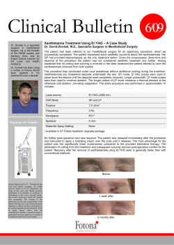


© Copyright 2026