
78K0S/Kx1+ Application Note Sample Program (Interrupt)
Application Note
78K0S/Kx1+
Sample Program (Interrupt)
External Interrupt Generated by Switch Input
This document describes an operation overview of the sample program, as well as how to use the sample
program and how to set and use the interrupt function. In the sample program, an interrupt is generated by
detecting the falling edge of the switch input and an LED lighting pattern is displayed according to the
number of switch inputs.
Target devices
78K0S/KA1+ microcontroller
78K0S/KB1+ microcontroller
78K0S/KU1+ microcontroller
78K0S/KY1+ microcontroller
Document No. U18812EJ1V0AN00 (1st edition)
Date Published October 2007 N
2007
Printed in Japan
CONTENTS
CHAPTER 1 OVERVIEW ....................................................................................3
1.1 Main Contents of Initial Settings ..............................................................3
1.2 Contents Following the Main Loop...........................................................4
CHAPTER 2 CIRCUIT DIAGRAM .......................................................................5
2.1 Circuit Diagram ........................................................................................5
2.2 Peripheral Hardware ................................................................................5
CHAPTER 3 SOFTWARE ...................................................................................6
3.1 File Configuration.....................................................................................6
3.2 Internal Peripheral Functions to Be Used ................................................7
3.3 Initial Settings and Operation Overview...................................................7
3.4 Flow Chart ...............................................................................................8
CHAPTER 4 SETTING METHODS .....................................................................9
4.1 Interrupt Setting .......................................................................................9
4.2 Processing During Interrupt ...................................................................15
CHAPTER 5 OPERATION CHECK USING SYSTEM SIMULATOR SM+ .......18
5.1 Building the Sample Program ................................................................18
5.2 Operation with SM+ ...............................................................................19
CHAPTER 6 RELATED DOCUMENTS............................................................24
APPENDIX A PROGRAM LIST.........................................................................25
APPENDIX B REVISION HISTORY ..................................................................34
• The information in this document is current as of June, 2007. The information is subject to change
without notice. For actual design-in, refer to the latest publications of NEC Electronics data sheets or
data books, etc., for the most up-to-date specifications of NEC Electronics products. Not all
products and/or types are available in every country. Please check with an NEC Electronics sales
representative for availability and additional information.
• No part of this document may be copied or reproduced in any form or by any means without the prior
written consent of NEC Electronics. NEC Electronics assumes no responsibility for any errors that may
appear in this document.
• NEC Electronics does not assume any liability for infringement of patents, copyrights or other intellectual
property rights of third parties by or arising from the use of NEC Electronics products listed in this document
or any other liability arising from the use of such products. No license, express, implied or otherwise, is
granted under any patents, copyrights or other intellectual property rights of NEC Electronics or others.
• Descriptions of circuits, software and other related information in this document are provided for illustrative
purposes in semiconductor product operation and application examples. The incorporation of these
circuits, software and information in the design of a customer's equipment shall be done under the full
responsibility of the customer. NEC Electronics assumes no responsibility for any losses incurred by
customers or third parties arising from the use of these circuits, software and information.
• While NEC Electronics endeavors to enhance the quality, reliability and safety of NEC Electronics products,
customers agree and acknowledge that the possibility of defects thereof cannot be eliminated entirely. To
minimize risks of damage to property or injury (including death) to persons arising from defects in NEC
Electronics products, customers must incorporate sufficient safety measures in their design, such as
redundancy, fire-containment and anti-failure features.
• NEC Electronics products are classified into the following three quality grades: "Standard", "Special" and
"Specific".
The "Specific" quality grade applies only to NEC Electronics products developed based on a customerdesignated "quality assurance program" for a specific application. The recommended applications of an NEC
Electronics product depend on its quality grade, as indicated below. Customers must check the quality grade of
each NEC Electronics product before using it in a particular application.
"Standard": Computers, office equipment, communications equipment, test and measurement equipment, audio
and visual equipment, home electronic appliances, machine tools, personal electronic equipment
and industrial robots.
"Special": Transportation equipment (automobiles, trains, ships, etc.), traffic control systems, anti-disaster
systems, anti-crime systems, safety equipment and medical equipment (not specifically designed
for life support).
"Specific": Aircraft, aerospace equipment, submersible repeaters, nuclear reactor control systems, life
support systems and medical equipment for life support, etc.
The quality grade of NEC Electronics products is "Standard" unless otherwise expressly specified in NEC
Electronics data sheets or data books, etc. If customers wish to use NEC Electronics products in applications
not intended by NEC Electronics, they must contact an NEC Electronics sales representative in advance to
determine NEC Electronics' willingness to support a given application.
(Note)
(1) "NEC Electronics" as used in this statement means NEC Electronics Corporation and also includes its
majority-owned subsidiaries.
(2) "NEC Electronics products" means any product developed or manufactured by or for NEC Electronics (as
defined above).
M8E 02. 11-1
2
Application Note U18812EJ1V0AN
CHAPTER 1 OVERVIEW
In this sample program, an example of using the interrupt function is presented. An LED lighting pattern is
displayed according to the number of switch inputs, by detecting the falling edge of the switch input and performing
interrupt servicing.
1.1
Main Contents of Initial Settings
The contents of the initial settings are as follows.
• Selecting the high-speed internal oscillator as the system clock sourceNote
• Stopping watchdog timer operation
• Setting the CPU clock frequency and peripheral hardware clock frequency to 2 MHz
• Setting I/O ports
• Setting the valid edge of INTP1 (external interrupt) to the falling edge
• Enabling interrupt
Note This is set by using the option byte.
Application Note U18812EJ1V0AN
3
CHAPTER 1 OVERVIEW
1.2
Contents Following the Main Loop
Interrupt servicing is performed by detecting the falling edge of the INTP1 pin, caused by switch input. In interrupt
servicing, the LED lighting pattern is changed by confirming that the switch is on, after about 10 ms have elapsed after
the falling edge of the INTP1 pin was detected. If the switch is off, after about 10 ms have elapsed, processing is
identified as chattering and the LED lighting pattern is not changed.
<Input>
<Output>
Switch turned on once
(kept on at least 10 ms)
78K0S/Kx1+
78K0S/Kx1+ microcontroller
SW
Note
LED2
LED1
LED Output
Number of Switch
Inputs
LED3
LED3
LED2
LED1
0
OFF
OFF
OFF
1
OFF
OFF
ON
2
OFF
ON
OFF
3
OFF
ON
ON
4
ON
OFF
OFF
5
ON
OFF
ON
6
ON
ON
OFF
7
ON
ON
ON
Note The lighting patterns from the zeroth switch input are repeated after the eighth switch input.
Caution
For cautions when using the device, refer to the user’s manual of each product (78K0S/KU1+,
78K0S/KY1+, 78K0S/KA1+, 78K0S/KB1+).
[Column] Chattering
Chattering is a phenomenon in which the electric signal repeats turning on and off due to a mechanical
flip-flop of the contacts, immediately after the switch has been pressed.
4
Application Note U18812EJ1V0AN
CHAPTER 2 CIRCUIT DIAGRAM
This chapter describes a circuit diagram and the peripheral hardware to be used in this sample program.
2.1
Circuit Diagram
A circuit diagram is shown below.
VDD
VDD
VDD
RESET
VSS
78K0S/Kx1+ P22
microcontroller
VDD
LED3
VDD
LED2
VDD
P21
LED1
SW
Note
INTP1
P20
Note INTP1/P43: 78K0S/KA1+ and 78K0S/KB1+ microcontrollers
INTP1/P32: 78K0S/KY1+ and 78K0S/KU1+ microcontrollers
Cautions 1. Connect the AVREF pin directly to VDD (only for the 78K0S/KA1+ and 78K0S/KB1+
microcontrollers).
2. Connect the AVSS pin directly to GND (only for the 78K0S/KB1+ microcontroller).
3. Leave all unused pins open (unconnected), except for the pins shown in the circuit diagram
and the AVREF and AVSS pins.
2.2
Peripheral Hardware
The peripheral hardware to be used is shown below.
(1) Switch (SW)
A switch is used as an input to control the lighting of an LED.
(2) LEDs (LED1, LED2, LED3)
The LEDs are used as outputs corresponding to switch inputs.
Application Note U18812EJ1V0AN
5
CHAPTER 3 SOFTWARE
This chapter describes the file configuration of the compressed file to be downloaded, internal peripheral functions
of the microcontroller to be used, and initial settings and operation overview of the sample program, and shows a flow
chart.
3.1
File Configuration
The following table shows the file configuration of the compressed file to be downloaded.
File Name
Description
main.asm
Source file for hardware initialization processing and main
(Assembly language
processing of microcontroller
Compressed (*.zip) File Included
zNote 1
zNote 1
z
z
version)
main.c
(C language version)
Assembler source file for setting the option byte (sets the
op.asm
system clock source)
int.prw
Work space file for integrated development environment PM+
z
int.prj
Project file for integrated development environment PM+
z
int.pri
Project files for system simulator SM+ for 78K0S/Kx1+
zNote 2
I/O panel file for system simulator SM+ for 78K0S/Kx1+ (used
zNote 2
int.prs
int.prm
int0.pnl
z
for checking peripheral hardware operations)
Timing chart file for system simulator SM+ for 78K0S/Kx1+
int0.wvo
z
(used for checking waveforms)
Notes 1. “main.asm” is included with the assembly language version, and “main.c” with the C language version.
2.
Remark
These files are not included among the files for the 78K0S/KU1+ microcontroller.
: Only the source file is included.
: The files to be used with integrated development environment PM+ and 78K0S/Kx1+ system
simulator SM+ are included.
: The microcontroller operation simulation file to be used with system simulator SM+ for
78K0S/Kx1+ is included.
6
Application Note U18812EJ1V0AN
CHAPTER 3 SOFTWARE
3.2
Internal Peripheral Functions to Be Used
The following internal peripheral functions of the microcontroller are used in this sample program.
• Switch input: INTP1Note (external interrupt)
• LED output: P20, P21, P22 (output ports)
Note INTP1/P43: 78K0S/KA1+ and 78K0S/KB1+ microcontrollers
INTP1/P32: 78K0S/KY1+ and 78K0S/KU1+ microcontrollers
3.3
Initial Settings and Operation Overview
In this sample program, the selection of the clock frequency, setting of the I/O ports, setting of interrupts, and the
like are performed in the initial settings.
After completion of the initial settings, interrupt servicing is performed by detecting the falling edge of the switch
input (SW) and the lighting of the three LEDs (LED1, LED2, and LED3) is controlled according to the number of switch
inputs.
The details are described in the state transition diagram shown below.
Initial settings
•
•
•
•
•
•
•
Referencing the option byte
• Selecting the high-speed internal oscillator as
the system clock source
• The low-speed internal oscillator can be stopped
by software.
• The P34/RESET pin is used as the RESET pin.
Stack pointer setting
Stopping watchdog timer operation
Setting the CPU clock frequency and peripheral
hardware clock frequency to 2 MHz
Stopping the oscillation of the low-speed internal
oscillator
I/O port setting
• Setting only P43/INTP1Note as an input port and
using an internal pull-up resistor
• P20 = P21 = P22 = 1
(LED1 = LED2 = LED3 = OFF)
Interrupt setting
• Setting the valid edge of INTP1 (external
interrupt) to the falling edge
• Enabling interrupt
LED lighting patterns
Waiting for switch input
INTP1 falling edge
detection
INTP1 = High level
(chattering detection)
10 ms wait
Clearing the INTP1
interrupt request
No. of SW inputs LED3
OFF
0
OFF
1
OFF
2
OFF
3
ON
4
ON
5
ON
6
ON
7
INTP1 = Low level
LED2
OFF
OFF
ON
ON
OFF
OFF
ON
ON
LED1
OFF
ON
OFF
ON
OFF
ON
OFF
ON
* The lighting patterns from the zeroth switch input
are repeated after the eighth switch input.
Note INTP1/P43: 78K0S/KA1+ and 78K0S/KB1+ microcontrollers
INTP1/P32: 78K0S/KY1+ and 78K0S/KU1+ microcontrollers
Application Note U18812EJ1V0AN
7
CHAPTER 3 SOFTWARE
3.4
Flow Chart
A flow chart for the sample program is shown below.
<Processing after reset release>
<INTP1 (external interrupt) servicing>
Start
Interrupt servicing start
Referencing the option byteNote
Saving the AX register data
Stack pointer setting
Stopping watchdog
timer operation
10 ms wait
Setting the CPU clock
frequency to 2 MHz
Stopping the oscillation of the
low-speed internal oscillator
Clearing the INTP1
interrupt request
Initial settings
High level
INTP1 pin level
I/O port setting
Low level
Generating the data to be
displayed next
Initializing LED outputs
(turning all off)
INTP1 setting
LED outputs from port 2 (P2)
Enabling interrupt
Restoring the AX register data
Infinite loop
Return
Note Referencing the option byte is automatically performed by the microcontroller after reset release. In this
sample program, the following contents are set by referencing the option byte.
• Using the high-speed internal oscillation clock (8 MHz (TYP.)) as the system clock source
• The low-speed internal oscillator can be stopped by using software
• Using the P34/RESET pin as the RESET pin
8
Application Note U18812EJ1V0AN
CHAPTER 4 SETTING METHODS
This chapter describes how to set interrupts, as well as interrupt servicing.
For other initial settings, refer to the 78K0S/Kx1+ Sample Program (Initial Settings) LED Lighting Switch
Control Application Note.
For how to set registers, refer to the user’s manual of each product (78K0S/KU1+, 78K0S/KY1+, 78K0S/KA1+,
78K0S/KB1+).
For assembler instructions, refer to the 78K/0S Series Instructions User’s Manual.
4.1
Interrupt Setting
The interrupt functions are controlled by using the following four types of registers.
• Interrupt request flag registers 0, 1Note (IF0, IF1Note)
• Interrupt mask flag registers 0, 1Note (MK0, MK1Note)
• External interrupt mode registers 0, 1Note (INTM0, INTM1Note)
• Program status word (PSW)
The names of interrupt request flags and interrupt mask flags for various interrupt requests are shown below.
Interrupt Request Signal Name
Interrupt Request Flag
Interrupt Mask Flag
INTLVI
LVIIF
LVIMK
INTP0
PIF0
PMK0
INTP1
PIF1
PMK1
INTTMH1
TMIFH1
TMMKH1
INTTM000
TMIF000
TMMK000
INTTM010
TMIF010
TMMK010
INTAD
ADIF
ADMK
INTP2
INTP3
Note
Note
INTTM80
Note
INTSRE6
INTSR6
INTST6
Note
Note
Note
PIF2
PIF3
Note
PMK2
Note
PMK3
Note
TMIF80
SREIF6
SRIF6
STIF6
Note
Note
TMMK80
Note
Note
Note
SREMK6
Note
SRMK6
Note
STMK6
Note
Note
Note Only 78K0S/KA1+ and 78K0S/KB1+ microcontrollers
Application Note U18812EJ1V0AN
9
CHAPTER 4 SETTING METHODS
(1) Interrupt request flag setting
An interrupt request flag is set to 1 when the corresponding interrupt request is generated, or when an
instruction is executed. It is cleared to 0 when an interrupt request is acknowledged, a reset is executed, or an
instruction is executed.
To use the interrupt function, clear to 0 the interrupt request flag to be used before the interrupt request is
generated.
Figure 4-1. Format of Interrupt Request Flag Registers 0, 1Note (IF0, IF1Note)
IF0
ADIF
TMIF
TMIF
TMIFH
010
000
1
STIF6
SRIF6
SREIF6
Note
Note
Note
PIF1
PIF0
LVIIF
0
IF1Note
0
TMIF
PIF3
Note
PIF2
Note
0
Note
80
Interrupt request flag
0
No interrupt request signal has been generated.
1
An interrupt request signal has been generated
and an interrupt is being requested.
(2) Interrupt servicing enable/disable setting
An interrupt mask flag is used to enable (0) or disable (1) the corresponding interrupt servicing.
To use the interrupt function, clear to 0 the interrupt mask flag to be used before the interrupt request is
generated.
Figure 4-2. Format of Interrupt Mask Flag Registers 0, 1Note (MK0, MK1Note)
MK0
ADMK
TMMK TMMK TMMK
010
000
PMK1
PMK0
LVIMK
1
TMMK
PMK3
PMK2
1
Note
Note
H1
MK1Note
1
STMK6 SRMK6
Note
Note
SRE
MK6
Note
Note
80
Interrupt servicing control
0
Enables interrupt servicing.
1
Disables interrupt servicing.
Note Only 78K0S/KA1+ and 78K0S/KB1+ microcontrollers
10
Application Note U18812EJ1V0AN
CHAPTER 4 SETTING METHODS
(3) External interrupt valid edge setting
INTM0 and INTM1Note are used to set the valid edges of INTP0, INTP1, INTP2Note, and INTP3Note (external
interrupts).
Figure 4-3. Format of External Interrupt Mode Registers 0 and 1Note (INTM0, INTM1Note)
INTM0
ES21
Note
ES20
Note
ES11
ES10
ES01
ES00
0
0
0
0
0
0
INTM1Note
0
0
ES31
Note
ES30
Note
INTPn valid edge selection (n = 0, 1, 2Note, 3Note)
0
0
Falling edge
0
1
Rising edge
1
0
Setting prohibited
1
1
Both rising and falling edges
The combinations of external interrupts and valid edge setting flags are shown below.
Setting Flag
External Interrupt
Note
INTP3Note
ES21Note
ES20Note
INTP2Note
ES11
ES10
INTP1
ES01
ES00
INTP0
ES31
Note
ES30
Note Only 78K0S/KA1+ and 78K0S/KB1+ microcontrollers
(4) Interrupt enable/disable setting
The IE flag of the program status word (PSW) is used to enable (1) or disable (0) interrupt. The IE flag can be
manipulated by using a dedicated instruction (EI: enable interrupt, DI: disable interrupt).
When the interrupt mask flag is cleared to 0 and the IE flag is set to 1, an interrupt request is generated and an
interrupt is acknowledged when the interrupt request flag is set to 1.
When the interrupt is acknowledged, the PSW is automatically saved to the stack and the IE flag is cleared to 0.
Figure 4-4. Format of Program Status Word (PSW)
PSW
IE
Z
0
AC
0
0
1
CY
Used in the execution of normal instructions
Enabling or disabling of interrupt acknowledgment
0
Disabled
1
Enabled
Application Note U18812EJ1V0AN
11
CHAPTER 4 SETTING METHODS
[Example] Performing interrupt servicing by detecting the falling edge of INTP1 (same content as the sample program
setting)
z Register settings
• Clearing to 0 the interrupt request flag (PIF1) corresponding to INTP1
• Clearing to 0 the interrupt mask flag (PMK1) corresponding to INTP1
• Setting the valid edge of INTP1 to “Falling edge”
• Enabling interrupt by executing the EI instruction
IF0
0
0
0
0
0
0
0
0
Interrupt request flag
0
No interrupt request signal has been generated.
MK0
1
1
1
1
0
1
1
1
Interrupt servicing control
0
Enables interrupt servicing.
INTM0
0
0
0
0
0
0
0
0
INTP1 valid edge selection
0
0
Falling edge
PSW
1
0
0
0
0
0
1
0
Enabling or disabling of interrupt acknowledgment
1
Remark
Enabled
Set the port shared with INTP1 (P43: 78K0S/KA1+ and 78K0S/KB1+ microcontrollers, P32:
78K0S/KY1+ and 78K0S/KU1+ microcontrollers) to “Input port”. Furthermore, set to “Use internal pullup resistors” because the circuit configuration in this sample program is set not to connect pull-up
resistors outside the microcontroller. The use of the internal pull-up resistors is not a setting required
when using external interrupts.
For the port settings, refer to 78K0S/Kx1+ Sample Program (Initial Settings) LED Lighting Switch
Control Application Note.
12
Application Note U18812EJ1V0AN
CHAPTER 4 SETTING METHODS
z Assembly language program example
(Same content as the 78K0S/KB1+ microcontroller sample program setting)
XVCT
CSEG
DW
DW
DW
DW
DW
DW
DW
DW
DW
DW
DW
DW
DW
DW
DW
DW
DW
XMAIN CSEG
RESET_START:
AT
0000H
RESET_START
RESET_START
RESET_START
RESET_START
RESET_START
INTERRUPT_P1
RESET_START
RESET_START
RESET_START
RESET_START
RESET_START
RESET_START
RESET_START
RESET_START
RESET_START
RESET_START
RESET_START
•
•
•
UNIT
INTP1 settings
Enabling of
interrupt
MOV
CLR1
CLR1
EI
MAIN_LOOP:
NOP
BR
Interrupt servicing is started
from the “INTERRUPT_P1” symbol when
an interrupt is generated, by describing the
initial value (“INTERRUPT_P1”) using the
DW pseudo instruction.
•
•
•
Setting P43 shared with the
INTP1 pin as an input port
MOV
MOV
MOV
;(00) RESET
;(02) -;(04) -;(06) INTLVI
;(08) INTP0
;(0A) INTP1
;(0C) INTTMH1
;(0E) INTTM000
;(10) INTTM010
;(12) INTAD
;(14) -;(16) INTP2
;(18) INTP3
;(1A) INTTM80
;(1C) INTSRE6
;(1E) INTSR6
;(20) INTST6
P4,
PU4,
PM4,
#00000000B
#00001000B
#00001000B
•
•
•
INTM0, #00000000B
PIF1
PMK1
$MAIN_LOOP
;Set output latches of P40-P47 as low
;Connect on-chip pull-up resistor to P43
;Set P43 as input mode, P40-P42 and
;P44-P47 as output mode
;Set the valid edge of INTP1 to falling edge
;Clear invalid interrupt requests in advance
;Release the INTP1 interrupt mask
;Enable vector interrupt
;Go to the MAIN_LOOP
INTERRUPT_P1:
PUSH
AX
•
•
•
Interrupt servicing is started from
“INTERRUPT_P1” by detecting the valid
edge (falling edge) of INTP1.
RETI
Application Note U18812EJ1V0AN
13
CHAPTER 4 SETTING METHODS
z C language program example
(Same content as the 78K0S/KB1+ microcontroller sample program setting)
#pragma interrupt INTP1 fn_intp1
•
•
•
void hdwinit(void){
Setting P43 shared with
the INTP1 pin as an input
port
P4
PU4
PM4
•
•
•
= 0b00000000;
= 0b00001000;
= 0b00001000;
/* Interrupt function declaration: INTP1 */
Interrupt servicing is started from the interrupt
function declared with the _interrupt modifier
when an interrupt is generated, by declaring
the INTP1 interrupt function (“fn_intp1” in this
case) in the preprocessing directive (#pragma
directive) and declaring that interrupt function
using the _interrupt modifier.
/* Set output latches of P40-P47 as low */
/* Connect on-chip pull-up resistor to P43 */
/* Set P43 as input mode, P40-P42 and */
/* P44-P47 as output mode */
•
•
•
INTM0 = 0b00000000;
PIF1 = 0;
PMK1 = 0;
/* Set the valid edge of INTP1 to falling edge */
/* Clear invalid interrupt requests in advance */
/* Release the INTP1 interrupt mask */
INTP1 settings
return;
}
void main(void){
Enabling of
interrupt
EI();
while (1){
NOP();
NOP();
}
}
/* Enable vector interrupt */
Interrupt servicing is started from
“fn_intp1” by detecting the valid edge
(falling edge) of INTP1.
__interrupt void fn_intp1(){
unsigned int unChat; /* 16-bit variable for the chattering removal timer */
•
•
•
return;
}
14
Application Note U18812EJ1V0AN
CHAPTER 4 SETTING METHODS
4.2
Processing During Interrupt
The processing during interrupt is described below.
(1) Assembly language
The following operations are performed in the assembly language processing during interrupt.
<1>
An interrupt request is generated by switch input and interrupt servicing is started.
<2>
AX register data is saved to the stack.
<3>
Processing waits for 10 ms.
<4>
PIF1 (INTP1 interrupt request flag) is cleared to 0.
<5>
The pin status of INTP1/P43Note is checked.
• INTP1/P43Note = Low level → <5>
• INTP1/P43Note = High level (chattering detection) → <9>
<6>
The P2 data currently output is read.
<7>
The read data is decremented by 1.
<8>
The values of bits other than bits 0 to 2, among the data in <7>, are set to 0.
<9>
The data in <8> is output to P2.
<10> The data saved to the stack is restored to the AX register.
<11> Processing is returned from interrupt servicing.
Note INTP1/P43: 78K0S/KA1+ and 78K0S/KB1+ microcontrollers
INTP1/P32: 78K0S/KY1+ and 78K0S/KU1+ microcontrollers
Remarks 1. <1> to <11> mentioned above correspond to <1> to <11> on the next page.
2. The content of the program example on the next page is the same as that of the 78K0S/KB1+
microcontroller sample program.
Application Note U18812EJ1V0AN
15
CHAPTER 4 SETTING METHODS
RAM area setting
XRAM
DSEG
CNT_1: DS
CNT_2: DS
SADDR
1
1
; For major loop
; For minor loop
Saves the work area (1 byte × 2)
of RAM to be used for interrupt
servicing.
Interrupt servicing
<1>
<2>
INTERRUPT_P1:
PUSH AX
;-----
; Save the AX register data to the stack
10 ms wait to handle chattering ----MOV
CNT_1, #28
; Assign the count value for the major loop
NOP
(a) 6 clocks
MOV
CNT_2,
#70
(c) 6 clocks
NOP
DBNZ
DBNZ
CLR1
CNT_2,
CNT_1,
PIF1
$LOOP_2
$LOOP_1
LOOP_1:
<3>
(d) 2 clocks
; Minor loop
; Major loop
; Clear the INTP1 interrupt request
;-----
Identification of chattering detection ----BT
P4.3,
$END_INTP1 ; Branch if there is no switch input
;-----
LED lighting processing ----MOV
A,
P2
; Read the current output value
DEC
A
; Decrement the A register value by 1
AND
A,
#00000111B ; Mask bits other than bits 0 to 2
MOV
P2,
A
; Output the LED light
<5>
(e) 8 clocks
(f) 8 clocks
INTP1/P43 = Low level
END_INTP1:
POP
RETI
<10>
<11>
; Assign the count value for the minor loop
(b) 2 clocks
LOOP_2:
<4>
<6>
<7>
<8>
<9>
Number of
clocks of the
instruction
INTP1/P43 = High level (chattering detection)
AX
; Restore the AX register data
; Return from interrupt servicing
Correspondences between the input data and output data are shown below.
Note
P22, P21, P20 Output Data
LED Lighting
Number of Switch Inputs
0
P22 = P21 = P20 = 1
7
Turns off all LEDs.
1
P22 = P21 = 1, P20 = 0
6
LED3, LED2: off, LED1: on
2
P22 = 1, P21 = 0, P20 = 1
5
LED3: off, LED2: on, LED1: off
3
P22 = 1, P21 = P20 = 0
4
LED3: off, LED2, LED1: on
4
P22 = 0, P21 = P20 = 1
3
LED3: on, LED2, LED1: off
5
P22 = 0, P21 = 1, P20 = 0
2
LED3: on, LED2: off, LED1: on
6
P22 = P21 = 0, P20 = 1
1
LED3, LED2: on, LED1: off
7
P22 = P21 = P20 = 0
0
Lights all LEDs.
Note The lighting patterns from the zeroth switch input are repeated after the eighth switch input.
Remarks 1. The wait time (10 ms) at <3> indicated above can be calculated by the following expressions.
• 1 clock = 1/2 MHz = 0.5 μs
• Number of clocks at <3> = (a) + (b) + { (c) + ((d) + (e)) × 70 + (f) } × 28
Repeats (c) to (f)
28 times
Repeats (d) + (e) 70 times
• Wait time at <3> = [ (a) + (b) + { (c) + ((d) + (e)) × 70 + (f) } × 28] × 0.5 μs
= [ 6 + 2 + {6 + (2 + 8) × 70 + 8} × 28] × 0.5 μs
= 20,000 × 0.5 μs = 10,000 μs = 10 ms
2. <1> to <11> mentioned above correspond to <1> to <11> on the previous page.
16
Application Note U18812EJ1V0AN
CHAPTER 4 SETTING METHODS
(2) C language
Similar operation as with the assembly language is performed with C language interrupt servicing.
Remark
The content of the following program example is the same as that of the 78K0S/KB1+
microcontroller sample program.
Interrupt servicing
__interrupt void fn_intp1(){
unsigned int unChat;
/* 16-bit variable for the chattering
removal timer */
for (unChat = 0; unChat < 278; unChat++){
/* Wait for about 10 ms (for chattering
removal) */
NOP();
}
PIF1 = 0;
if (!P4.3){
10 ms or more */
P2 = (P2 - 1) & 0b00000111;
SW inputs */
}
/* Clear the INTP1 interrupt request */
/* Processing performed if SW is on for
/* LED output according to the number of
return;
}
Correspondences between the input data and output data are shown below.
Note
P22, P21, P20 Output Data
LED Lighting
Number of Switch Inputs
0
P22 = P21 = P20 = 1
7
Turns off all LEDs.
1
P22 = P21 = 1, P20 = 0
6
LED3, LED2: off, LED1: on
2
P22 = 1, P21 = 0, P20 = 1
5
LED3: off, LED2: on, LED1: off
3
P22 = 1, P21 = P20 = 0
4
LED3: off, LED2, LED1: on
4
P22 = 0, P21 = P20 = 1
3
LED3: on, LED2, LED1: off
5
P22 = 0, P21 = 1, P20 = 0
2
LED3: on, LED2: off, LED1: on
6
P22 = P21 = 0, P20 = 1
1
LED3, LED2: on, LED1: off
7
P22 = P21 = P20 = 0
0
Lights all LEDs.
Note The lighting patterns from the zeroth switch input are repeated after the eighth switch input.
Application Note U18812EJ1V0AN
17
CHAPTER 5 OPERATION CHECK USING SYSTEM SIMULATOR SM+
This chapter describes how the sample program operates with system simulator SM+ for 78K0S/Kx1+, by using the
assembly language file that has been downloaded by selecting the
Caution
icon.
System simulator SM+ for 78K0S/Kx1+ is not supported with the 78K0S/KU1+ microcontroller (as
of June 2007). The operation of the 78K0S/KU1+ microcontroller can therefore not be checked by
using system simulator SM+ for 78K0S/Kx1+.
5.1
Building the Sample Program
To check the operation of the sample program by using system simulator SM+ for 78K0S/Kx1+ (hereinafter referred
to as “SM+”), SM+ must be started after building the sample program. This section describes an example of the
operation sequence, from building the sample program with integrated development environment PM+, using the
assembly language file that has been downloaded by selecting
, up to starting SM+.
For the details of how to operate PM+, refer to the PM+ Project Manager User’s Manual.
(1) Start PM+.
(2) Select “int.prw” by clicking [Open Workspace] from the [File] menu and click [Open]. A workspace into which
the source file will be automatically read will be created.
(3) Select [Project Settings] from the [Project] menu. When the [Project Settings] window opens, select the name
of the device to be used (the device with the largest ROM or RAM size will be selected by default), and click
[OK].
Click
Select the device name
Click the [OK] button
18
Application Note U18812EJ1V0AN
CHAPTER 5 OPERATION CHECK USING SYSTEM SIMULATOR SM+
(4) Click
([Build → Debug] button). When the “main.asm” and “op.asm” source files are built normally, the
message “I3500: Build completed normally.” will be displayed.
(5) Click the [OK] button in the message window to automatically start SM+.
Click
Click
SM+ starts automatically.
5.2
Operation with SM+
This section describes examples of checking the operation on the I/O panel window or timing chart window of SM+.
For the details of how to operate SM+, refer to the SM+ System Simulator Operation User’s Manual.
Application Note U18812EJ1V0AN
19
CHAPTER 5 OPERATION CHECK USING SYSTEM SIMULATOR SM+
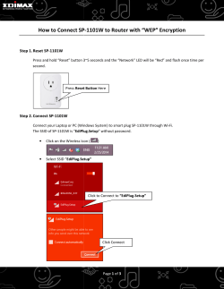
(1) When SM+ is started by clicking [Build → Debug] on PM+ (refer to 5.1), the following screen will be displayed.
(This is a screen example when the assembly language source file is used.)
(2) Click
([Restart] button). The program will be executed after the CPU is reset and the following screen will
be displayed.
Click
This turns red
during program
execution.
20
Application Note U18812EJ1V0AN
CHAPTER 5 OPERATION CHECK USING SYSTEM SIMULATOR SM+
(3) Click the [SW] button in the I/O panel window, during program execution.
Check that the lighting of [LED1] to [LED3] in the I/O panel window, as well as the waveforms in the timing
chart window change, depending on the number of [SW] button inputs.
I/O panel window
Timing chart window
P20: H output
All LEDs turn off.
P21: H output
P22: H output
Do not click.
P20: L output
Only LED1 lights.
P21: H output
P22: H output
Click once.
Note
P20: H output
Only LED2 lights.
P21: L output
P22: H output
Click twice.
•
•
•
•
•
•
P20: L output
All LEDs light.
P21: L output
P22: L output
Click seven times.
Note The lighting patterns from the zeroth switch input are repeated after the eighth switch input.
Remark
H: High level, L: Low level
Application Note U18812EJ1V0AN
21
CHAPTER 5 OPERATION CHECK USING SYSTEM SIMULATOR SM+
[Supplement 1] The changes in the data value of port 2 can be checked by using the SM+ watch function.
<1> Select [Watch] from the [Browse] menu to open the [Watch] window.
<2> Click [Add] to open the [Add Watch] window. (At this time, the [Watch] window is kept opened.)
<3> Enter “P2” in the [Name] field and click the [OK] button to register “P2” in the [Watch] window and close
the [Add Watch] window.
Enter “P2”, then click the
[OK] button.
Click
P2 is registered.
This is an example of the screen after
CPU reset. The data value of P2 is as
follows after CPU reset.
• P2: 0x00
<4> Execute the program and click the [SW] button in the I/O panel window. Check that the data value of P2
in the [Watch] window changes, depending on the number of [SW] button inputs.
Note
Number of [SW] Button Inputs
Data Value in [Watch] Window
0
P2: 0x07
1
P2: 0x06
2
P2: 0x05
3
P2: 0x04
4
P2: 0x03
5
P2: 0x02
6
P2: 0x01
7
P2: 0x00
Note The lighting patterns from the zeroth switch input are repeated after the eighth switch input.
22
Application Note U18812EJ1V0AN
CHAPTER 5 OPERATION CHECK USING SYSTEM SIMULATOR SM+
[Supplement 2] The [SW] button hold time can be set to less than 10 ms to check whether chattering is being
detected.
<1> Select
on the toolbar.
<2> Right-click the [SW] button in the I/O panel window and select [Properties].
<3> Enter “9” for the Hold Time and click the [OK] button.
Enter “9”, then click
the [OK] button.
<4> Select
on the toolbar.
<5> Execute the program and click the [SW] button. Even if the [SW] button is clicked, chattering will be
identified and the LED lighting pattern will not change, because the button hold time is 9 ms.
Application Note U18812EJ1V0AN
23
CHAPTER 6 RELATED DOCUMENTS
Document Name
78K0S/KU1+ User’s Manual
PDF
78K0S/KY1+ User’s Manual
PDF
78K0S/KA1+ User’s Manual
PDF
78K0S/KB1+ User’s Manual
PDF
78K/0S Series Instructions User’s Manual
PDF
RA78K0S Assembler Package User’s Manual
CC78K0S C Compiler User’s Manual
24
Japanese/English
Language
PDF
Operation
PDF
Language
PDF
Operation
PDF
PM+ Project Manager User’s Manual
PDF
SM+ System Simulator Operation User’s Manual
PDF
78K0S/Kx1+ Sample Program (Initial Settings) LED Lighting Switch Control Application Note
PDF
78K0S/Kx1+ Sample Program Startup Guide Application Note
PDF
Application Note U18812EJ1V0AN
APPENDIX A PROGRAM LIST
As a program list example, the 78K0S/KB1+ microcontroller source program is shown below.
z main.asm (Assembly language version)
;*****************************************************************************
;
;
NEC Electronics
78K0S/KB1+
;
;*****************************************************************************
;
78K0S/KB1+ Sample program
;*****************************************************************************
;
Interrupt
;*****************************************************************************
;<<History>>
;
2007.6.-Release
;*****************************************************************************
;
;<<Overview>>
;
;This sample program presents an example of using the interrupt function.
;An LED lighting pattern according to the number of switch inputs is displayed
;by detecting the falling edge of the switch input and generating an interrupt.
;Here, chattering within 10 ms will not be counted as a switch input, because
;a chattering removal time of 10 ms is set immediately after the interrupt.
;
;
; <Principal setting contents>
;
; - Set the vector table
; - Set the stack pointer
; - Stop the watchdog timer operation
; - Set the CPU clock frequency to 2 MHz
; - Set the valid edge of external interrupt INTP1 to falling edge
; - Set the chattering detection time during switch input to 10 ms;
;
;
; <Number of switch inputs and LED lighting patterns>
;
;
+------------------------------------+
;
| SW Inputs | LED3 | LED2 | LED1 |
;
|
(P43)
| (P22) | (P21) | (P20) |
;
|------------|-----------------------|
;
|
0 times | OFF | OFF | OFF |
;
|
1 time
| OFF | OFF | ON
|
;
|
2 times | OFF | ON
| OFF |
;
|
3 times | OFF | ON
| ON
|
;
|
4 times | ON
| OFF | OFF |
;
|
5 times | ON
| OFF | ON
|
;
|
6 times | ON
| ON
| OFF |
;
|
7 times | ON
| ON
| ON
|
;
+------------------------------------+
;
# The lighting patterns from the zeroth switch input are repeated after
the eighth switch input.
;
;
Application Note U18812EJ1V0AN
25
APPENDIX A PROGRAM LIST
;<<I/O port settings>>
;
; Input: P43
; Output: P00-P03, P20-P23, P30-P33, P40-P42, P44-P47, P120-P123, P130
; # All unused ports are set as the output mode.
;
;*****************************************************************************
;=============================================================================
;
;
Vector table
;
;=============================================================================
XVCT CSEG AT
0000H
DW
RESET_START
;(00) RESET
DW
RESET_START
;(02) -DW
RESET_START
;(04) -DW
RESET_START
;(06) INTLVI
DW
RESET_START
;(08) INTP0
DW
INTERRUPT_P1
;(0A) INTP1
DW
RESET_START
;(0C) INTTMH1
DW
RESET_START
;(0E) INTTM000
DW
RESET_START
;(10) INTTM010
DW
RESET_START
;(12) INTAD
DW
RESET_START
;(14) -DW
RESET_START
;(16) INTP2
DW
RESET_START
;(18) INTP3
DW
RESET_START
;(1A) INTTM80
DW
RESET_START
;(1C) INTSRE6
DW
RESET_START
;(1E) INTSR6
DW
RESET_START
;(20) INTST6
;=============================================================================
;
;
Define the RAM
;
;=============================================================================
XRAM DSEG SADDR
CNT_1:
DS
1
; For major loop
CNT_2:
DS
1
; For minor loop
;=============================================================================
;
;
Define the memory stack area
;
;=============================================================================
XSTK DSEG AT
0FEE0H
STACKEND:
DS
20H
; Memory stack area = 32 bytes
STACKTOP:
; Start address of the memory stack area = FF00H
;*****************************************************************************
;
;
Initialization after RESET
;
;*****************************************************************************
XMAIN CSEG UNIT
RESET_START:
26
Application Note U18812EJ1V0AN
APPENDIX A PROGRAM LIST
;----------------------------------------------------------------------------;
Initialize the stack pointer
;----------------------------------------------------------------------------MOVW AX,
#STACKTOP
MOVW SP,
AX
; Set the stack pointer
;----------------------------------------------------------------------------;
Initialize the watchdog timer
;----------------------------------------------------------------------------MOV
WDTM, #01110111B
; Stop the watchdog timer operation
;----------------------------------------------------------------------------;
Initialize the clock generators
;----------------------------------------------------------------------------MOV
PPCC, #00000010B
; The clock supplied to the peripheral
hardware (fxp) = fx/4 (= 2 MHz)
MOV
PCC,
#00000000B
; The clock supplied to the CPU (fcpu) = fxp
(= 2 MHz)
MOV
LSRCM, #00000001B
; Stop the oscillation of the low-speed
internal oscillator
;----------------------------------------------------------------------------;
Initialize the port 0
;----------------------------------------------------------------------------MOV
P0,
#00000000B
; Set output latches of P00-P03 as low
MOV
PM0,
#11110000B
; Set P00-P03 as output mode
;----------------------------------------------------------------------------;
Initialize the port 2
;----------------------------------------------------------------------------MOV
P2,
#00000111B
; Set output latches of P20-P22 as high (turn
off LED1-LED3), P23 as low
MOV
PM2,
#11110000B
; Set P20-P23 as output mode
;----------------------------------------------------------------------------;
Initialize the port 3
;----------------------------------------------------------------------------MOV
P3,
#00000000B
; Set output latches of P30-P33 as low
MOV
PM3,
#11110000B
; Set P30-P33 as output mode
;----------------------------------------------------------------------------;
Initialize the port 4
;----------------------------------------------------------------------------MOV
P4,
#00000000B
; Set output latches of P40-P47 as low
MOV
PU4,
#00001000B
; Connect on-chip pull-up resistor to P43
MOV
PM4,
#00001000B
; Set P43 as input mode, P40-P42 and P44-P47
as output mode
;----------------------------------------------------------------------------;
Initialize the port 12
;----------------------------------------------------------------------------MOV
P12,
#00000000B
; Set output latches of P120-P123 as low
MOV
PM12, #11110000B
; Set P120-P123 as output mode
;----------------------------------------------------------------------------;
Initialize the port 13
;----------------------------------------------------------------------------MOV
P13,
#00000001B
; Set output latch of P130 as high
Application Note U18812EJ1V0AN
27
APPENDIX A PROGRAM LIST
;----------------------------------------------------------------------------;
Set the interrupt
;----------------------------------------------------------------------------MOV
INTM0, #00000000B
; Set the valid edge of INTP1 to falling edge
CLR1 PIF1
; Clear invalid interrupt requests in advance
CLR1 PMK1
; Release the INTP1 interrupt mask
EI
; Enable vector interrupt
;*****************************************************************************
;
;
Main loop
;
;*****************************************************************************
MAIN_LOOP:
NOP
BR
$MAIN_LOOP
; Go to the MAIN_LOOP
;*****************************************************************************
;
;
External interrupt INTP1
;
;*****************************************************************************
INTERRUPT_P1:
PUSH AX
; Save the AX register data to the stack
;----- 10 ms wait
MOV
CNT_1,
NOP
LOOP_1:
MOV
CNT_2,
LOOP_2:
NOP
DBNZ CNT_2,
DBNZ CNT_1,
CLR1
to handle chattering ----#28
; Assign the count value for the major loop
#70
; Assign the count value for the minor loop
$LOOP_2
$LOOP_1
; Minor loop
; Major loop
PIF1
; Clear the INTP1 interrupt request
;----- Identification of chattering detection ----BT
P4.3, $END_INTP1
; Branch if there is no switch input
;----- LED
MOV
DEC
AND
MOV
lighting processing
A,
P2
A
A,
#00000111B
P2,
A
END_INTP1:
POP
RETI
AX
;
;
;
;
----Read the current output value
Decrement the A register value by 1
Mask bits other than bits 0 to 2
Output the LED light
; Restore the AX register data
; Return from interrupt servicing
end
28
Application Note U18812EJ1V0AN
APPENDIX A PROGRAM LIST
z main.c (C language version)
/***************************************************************************
NEC Electronics
78K0S/KB1+
****************************************************************************
78K0S/KB1+ Sample program
****************************************************************************
Interrupt
****************************************************************************
<<History>>
2007.6.-Release
****************************************************************************
<<Overview>>
This sample program presents an example of using the interrupt function.
An LED lighting pattern according to the number of switch inputs is
displayed by detecting the falling edge of the switch input and generating
an interrupt.
Here, chattering within 10 ms will not be counted as a switch input, because
a chattering removal time of 10 ms is set immediately after the interrupt.
<Principal setting contents>
-
Declare a function run by an interrupt: INTP1 -> fn_intp1()
Stop the watchdog timer operation
Set the CPU clock frequency to 2 MHz
Set the valid edge of external interrupt INTP1 to falling edge
Set the chattering detection time during switch input to 10 ms
<Number of switch inputs and LED lighting patterns>
+------------------------------------+
| SW Inputs | LED3 | LED2 | LED1 |
|
(P43)
| (P22) | (P21) | (P20) |
|------------|-----------------------|
|
0 times | OFF | OFF | OFF |
|
1 time
| OFF | OFF | ON
|
|
2 times | OFF | ON
| OFF |
|
3 times | OFF | ON
| ON
|
|
4 times | ON
| OFF | OFF |
|
5 times | ON
| OFF | ON
|
|
6 times | ON
| ON
| OFF |
|
7 times | ON
| ON
| ON
|
+------------------------------------+
# The lighting patterns from the zeroth switch input are repeated after
the eighth switch input.
<<I/O port settings>>
Input: P43
Output: P00-P03, P20-P23, P30-P33, P40-P42, P44-P47, P120-P123, P130
# All unused ports are set as the output mode.
Application Note U18812EJ1V0AN
29
APPENDIX A PROGRAM LIST
***************************************************************************/
/*==========================================================================
Preprocessing directive (#pragma)
==========================================================================*/
#pragma
SFR
/* SFR names can be described at the C
source level */
#pragma
EI
/* EI instructions can be described at the
C source level */
#pragma
NOP
/* NOP instructions can be described at
the C source level */
#pragma interrupt INTP1 fn_intp1 /* Interrupt function declaration:INTP1 */
/***************************************************************************
Initialization after RESET
***************************************************************************/
void hdwinit(void){
/*-------------------------------------------------------------------------Initialize the watchdog timer
--------------------------------------------------------------------------*/
WDTM = 0b01110111;
/* Stop the watchdog timer operation */
/*-------------------------------------------------------------------------Initialize the clock generators
--------------------------------------------------------------------------*/
PPCC = 0b00000010;
/* The clock supplied to the peripheral
hardware (fxp) = fx/4 (= 2 MHz) */
PCC
= 0b00000000;
/* The clock supplied to the CPU (fcpu) =
fxp (= 2 MHz) */
LSRCM = 0b00000001;
/* Stop the oscillation of the low-speed
internal oscillator */
/*-------------------------------------------------------------------------Initialize the port 0
--------------------------------------------------------------------------*/
P0
= 0b00000000;
/* Set output latches of P00-P03 as low */
PM0
= 0b11110000;
/* Set P00-P03 as output mode */
/*-------------------------------------------------------------------------Initialize the port 2
--------------------------------------------------------------------------*/
P2
= 0b00000111;
/* Set output latches of P20-P22 as high
(turn off LED1-LED3), P23 as low */
PM2
= 0b11110000;
/* Set P20-P23 as output mode */
/*-------------------------------------------------------------------------Initialize the port 3
--------------------------------------------------------------------------*/
P3
= 0b00000000;
/* Set output latches of P30-P33 as low */
PM3
= 0b11110000;
/* Set P30-P33 as output mode */
/*-------------------------------------------------------------------------Initialize the port 4
30
Application Note U18812EJ1V0AN
APPENDIX A PROGRAM LIST
--------------------------------------------------------------------------*/
P4
= 0b00000000;
/* Set output latches of P40-P47 as low */
PU4
= 0b00001000;
/* Connect on-chip pull-up resistor to P43 */
PM4
= 0b00001000;
/* Set P43 as input mode, P40-P42 and P44-P47 as
output mode */
/*-------------------------------------------------------------------------Initialize the port 12
--------------------------------------------------------------------------*/
P12
= 0b00000000;
/* Set output latches of P120-P123 as low */
PM12 = 0b11110000;
/* Set P120-P123 as output mode */
/*-------------------------------------------------------------------------Initialize the port 13
--------------------------------------------------------------------------*/
P13
= 0b00000001;
/* Set output latch of P130 as high */
/*-------------------------------------------------------------------------Set the interrupt
--------------------------------------------------------------------------*/
INTM0 = 0b00000000;
/* Set the valid edge of INTP1 to falling
edge */
PIF1 = 0;
/* Clear invalid interrupt requests in
advance */
PMK1 = 0;
/* Release the INTP1 interrupt mask */
return;
}
/***************************************************************************
Main loop
***************************************************************************/
void main(void){
EI();
/* Enable vector interrupt */
while (1){
NOP();
NOP();
}
}
/***************************************************************************
External interrupt INTP1
***************************************************************************/
__interrupt void fn_intp1(){
unsigned int unChat;
/* 16-bit variable for the chattering removal
timer */
for (unChat = 0; unChat < 278; unChat++){ /* Wait for about 10 ms (for
chattering removal) */
NOP();
}
PIF1
= 0;
/* Clear the INTP1 interrupt request */
Application Note U18812EJ1V0AN
31
APPENDIX A PROGRAM LIST
if (!P4.3){
/* Processing performed if SW is on for 10 ms or
more */
P2 = (P2 - 1) & 0b00000111; /* LED output according to the
number of SW inputs */
}
return;
}
32
Application Note U18812EJ1V0AN
APPENDIX A PROGRAM LIST
z op.asm (Common to assembly language and C language versions)
;===========================================================================
;
;
Option byte
;
;===========================================================================
OPBTCSEG AT
0080H
DB
10011100B
; Option byte area
;
||||
;
|||+--------- Low-speed
internal
oscillator
can
be
stopped by software
;
|++---------- High-speed internal oscillation clock (8
MHz) is selected for system clock source
;
+------------ P34/RESET pin is used as RESET pin
DB
mode)
;
;
11111111B
; Protect byte area (for the self programming
||||||||
++++++++--------- All blocks can be written or erased
end
Application Note U18812EJ1V0AN
33
APPENDIX B REVISION HISTORY
Edition
1st edition
34
Date Published
October 2007
Page
Revision
−
−
Application Note U18812EJ1V0AN
For further information,
please contact:
NEC Electronics Corporation
1753, Shimonumabe, Nakahara-ku,
Kawasaki, Kanagawa 211-8668,
Japan
Tel: 044-435-5111
http://www.necel.com/
[America]
[Europe]
[Asia & Oceania]
NEC Electronics America, Inc.
2880 Scott Blvd.
Santa Clara, CA 95050-2554, U.S.A.
Tel: 408-588-6000
800-366-9782
http://www.am.necel.com/
NEC Electronics (Europe) GmbH
Arcadiastrasse 10
40472 Düsseldorf, Germany
Tel: 0211-65030
http://www.eu.necel.com/
NEC Electronics (China) Co., Ltd
7th Floor, Quantum Plaza, No. 27 ZhiChunLu Haidian
District, Beijing 100083, P.R.China
Tel: 010-8235-1155
http://www.cn.necel.com/
Hanover Office
Podbielskistrasse 166 B
30177 Hannover
Tel: 0 511 33 40 2-0
Munich Office
Werner-Eckert-Strasse 9
81829 München
Tel: 0 89 92 10 03-0
Stuttgart Office
Industriestrasse 3
70565 Stuttgart
Tel: 0 711 99 01 0-0
United Kingdom Branch
Cygnus House, Sunrise Parkway
Linford Wood, Milton Keynes
MK14 6NP, U.K.
Tel: 01908-691-133
Succursale Française
9, rue Paul Dautier, B.P. 52
78142 Velizy-Villacoublay Cédex
France
Tel: 01-3067-5800
Sucursal en España
Juan Esplandiu, 15
28007 Madrid, Spain
Tel: 091-504-2787
Tyskland Filial
Täby Centrum
Entrance S (7th floor)
18322 Täby, Sweden
Tel: 08 638 72 00
Filiale Italiana
Via Fabio Filzi, 25/A
20124 Milano, Italy
Tel: 02-667541
Shanghai Branch
Room 2509-2510, Bank of China Tower,
200 Yincheng Road Central,
Pudong New Area, Shanghai, P.R.China P.C:200120
Tel:021-5888-5400
http://www.cn.necel.com/
Shenzhen Branch
Unit 01, 39/F, Excellence Times Square Building,
No. 4068 Yi Tian Road, Futian District, Shenzhen,
P.R.China P.C:518048
Tel:0755-8282-9800
http://www.cn.necel.com/
NEC Electronics Hong Kong Ltd.
Unit 1601-1613, 16/F., Tower 2, Grand Century Place,
193 Prince Edward Road West, Mongkok, Kowloon, Hong Kong
Tel: 2886-9318
http://www.hk.necel.com/
NEC Electronics Taiwan Ltd.
7F, No. 363 Fu Shing North Road
Taipei, Taiwan, R. O. C.
Tel: 02-8175-9600
http://www.tw.necel.com/
NEC Electronics Singapore Pte. Ltd.
238A Thomson Road,
#12-08 Novena Square,
Singapore 307684
Tel: 6253-8311
http://www.sg.necel.com/
NEC Electronics Korea Ltd.
11F., Samik Lavied’or Bldg., 720-2,
Yeoksam-Dong, Kangnam-Ku,
Seoul, 135-080, Korea
Tel: 02-558-3737
http://www.kr.necel.com/
Branch The Netherlands
Steijgerweg 6
5616 HS Eindhoven
The Netherlands
Tel: 040 265 40 10
G0706


© Copyright 2026