
ニュー 09 09004 09000
0
00
0
09
00
04
40
1
00
00
00
00
0
Fc
C 12w
M
P
0
0
00
0
00
09
04
40
1
0
0
00
09
0
00
SU 211
B w
19
7
Fc
P
2
c1
M
C
00
1
0
6
F
0
90
0
44
1
0
07
35
6
07
35
7
09
0
00
5
73
6
0
1
0
44
C
M
P
00
0
0
40
4
19
00
0
w
12
Fc
00
00
04
1W
21
FC
09
00
0
SU
B
07
35
7
09
Sample of programs
07
35
4
00
ニュー
09
0
>
w
16 F-5
→ 1
4 0
90
04
09
00
4
FI 70w
LE
F-
F
O -4
N 7
LS
FFI 70W
LE
00
00
0
F
O -4
N 7
LS
04
40
0
Version 1.0
Produced in March 1997
51
F-
F-
0
00
00
02
09
00
0
04
40
1
00
16
1
→
09
4 0
FC
00
90
0
04
C 12
M W
09
P
09
00
09
00
4
00
6
4
00
00
00
04
40
0
Sharp Programmable Controller
NEW
00
0
F
O -4
N 8
LR
4
5
73
00
Fc
SU 211
B w
09
00
09
4
5
73
Fc
M 215
U
L
0
4
09
F
04
40
2
00
00
02
00
09
00
6
1
00
4
04
01
w
12
Fc
00
04
00
1w
21
c
F
09
0
00
19
09
4 0
90
04
→
51
F-
SU
B
Fc
C 12
M w
P
16
00
09
C
M
P
07
35
7
FFI 70w
LE
F
O -4
N 7
LS
04
40
0
Satellite
00
07
35
7
07
35
4
40
0
¤
↓
04
2
40
0
0
00
2
0
44
2
0
5
73
7
0
00
0
Introduction
This booklet gave you hits of program plan using various kinds of program example with understood
the great variety and easy to use of application instructions of sharp programmable controller new
satellite JW series.
This booklet is composed of next four chapters and appendix. Please read only necessary passage.
Chapter 1 : Basic circuit
Chapter 2 : Data processing circuit
Chapter 3 : How to use special instruction
Chapter 4 : Example of applications program
Appendix : Description of instruction words
Refer to instruction manual, users manual , and programming manual of each programmable
controller in detail.
Note
・The contents of this manual have been carefully written. However, if you have a problem,
contact your dealer.
・The whole or partial photocopy of this booklet is prohibited.
・Contacts of this booklet may be revised for improvement without notice.
Table of contents
Prior to using this manual
Chapter 1: Basic circuit ••••••••••••••••••••••••••••••••••••••••••
1−1
1−2
1−3
1−4
1−5
1−6
1−7
1−8
1−9
1 −10
1 −11
1 −12
1 −13
1 −14
1 −15
1 −16
1 −17
1 −18
1 −19
1 −20
1 −21
1 −22
1 −23
1 −24
1 −25
1 −26
Normally circuit ••••••••••••••••••••••••••••••••••••••••••••••••••••••••••••••••••••••••••••
Circuit from which 1 pulse is generated at power ON •••••••••••••••••••••••••••••
Oscillation circuit ••••••••••••••••••••••••••••••••••••••••••••••••••••••••••••••••••••••••••
Rise edge differentiation ••••••••••••••••••••••••••••••••••••••••••••••••••••••••••••••••
Fall edge differentiation •••••••••••••••••••••••••••••••••••••••••••••••••••••••••••••••••
Self-hold circuit ( reset in priority ) •••••••••••••••••••••••••••••••••••••••••••••••••••••
Self-hold circuit ( set in priority ) •••••••••••••••••••••••••••••••••••••••••••••••••••••••
Priority circuit ••••••••••••••••••••••••••••••••••••••••••••••••••••••••••••••••••••••••••••••
Alternate circuit •••••••••••••••••••••••••••••••••••••••••••••••••••••••••••••••••••••••••••
n bit shift register •••••••••••••••••••••••••••••••••••••••••••••••••••••••••••••••••••••••••
ON delay timer ••••••••••••••••••••••••••••••••••••••••••••••••••••••••••••••••••••••••••••
OFF delay timer •••••••••••••••••••••••••••••••••••••••••••••••••••••••••••••••••••••••••••
ON/OFF delay timer ••••••••••••••••••••••••••••••••••••••••••••••••••••••••••••••••••••••
One shot timer at the input rise edge(1) •••••••••••••••••••••••••••••••••••••••••••••
One shot timer at the input rise edge(2) •••••••••••••••••••••••••••••••••••••••••••••
One shot timer at the input fall edge ••••••••••••••••••••••••••••••••••••••••••••••••••
One shot timer at rise/fall edge ••••••••••••••••••••••••••••••••••••••••••••••••••••••••
ON delay one shot timer ••••••••••••••••••••••••••••••••••••••••••••••••••••••••••••••••
Equivalent pulse generation circuit ••••••••••••••••••••••••••••••••••••••••••••••••••••
Duty variable pulse generator circuit(1) ••••••••••••••••••••••••••••••••••••••••••••••
Duty variable pulse generator circuit(2) ••••••••••••••••••••••••••••••••••••••••••••••
Long time timer(1) ••••••••••••••••••••••••••••••••••••••••••••••••••••••••••••••••••••••••
Long time timer(2) ••••••••••••••••••••••••••••••••••••••••••••••••••••••••••••••••••••••••
Large capacity counter(1) •••••••••••••••••••••••••••••••••••••••••••••••••••••••••••••••
Large capacity counter(2) •••••••••••••••••••••••••••••••••••••••••••••••••••••••••••••••
Counter that counts at the rise or fall edge of counter input •••••••••••••••••••••
Chapter 2 : Data processing circuit •••••••••••••••••••••••••••••
2−1
2−2
2−3
2−4
2−5
2−6
2−7
2−8
2−9
1•1 to 1•18
1• 1
1• 2
1• 3
1• 4
1• 4
1• 5
1• 6
1• 7
1• 8
1• 9
1•10
1•10
1•11
1•11
1•12
1•12
1•13
1•13
1•14
1•15
1•15
1•16
1•16
1•17
1•17
1•18
2•1 to 2•74
Change of operation execution condition •••••••••••••••••••••••••••••••••••••••••••••
Register clear ••••••••••••••••••••••••••••••••••••••••••••••••••••••••••••••••••••••••••••••
Masking data •••••••••••••••••••••••••••••••••••••••••••••••••••••••••••••••••••••••••••••••
Set/reset bits •••••••••••••••••••••••••••••••••••••••••••••••••••••••••••••••••••••••••••••••
Decomposition of number •••••••••••••••••••••••••••••••••••••••••••••••••••••••••••••••
Composition of number ••••••••••••••••••••••••••••••••••••••••••••••••••••••••••••••••••
Comparison with setting value ••••••••••••••••••••••••••••••••••••••••••••••••••••••••••
Window comparator •••••••••••••••••••••••••••••••••••••••••••••••••••••••••••••••••••••••
Comparator having undetectable zone •••••••••••••••••••••••••••••••••••••••••••••••
2• 1
2• 2
2• 2
2• 3
2• 4
2• 5
2• 6
2• 8
2• 9
2 −10
2 −11
2 −12
2 −13
2 −14
2 −15
2 −16
2 −17
2 −18
2 −19
2 −20
2 −21
2 −22
2 −23
2 −24
2 −25
2 −26
2 −27
2 −28
2 −29
2 −30
2 −31
2 −32
2 −33
2 −34
2 −35
2 −36
2 −37
2 −38
2 −39
2 −40
2 −41
2 −42
2 −43
2 −44
Timer that multiple number of set points ••••••••••••••••••••••••••••••••••••••••••••• 2•10
Obtaining the BCD result by the signed absolute value ••••••••••••••••••••••••••• 2•11
Multiplication of BCD 8 digits ••••••••••••••••••••••••••••••••••••••••••••••••••••••••••• 2•12
BCD 8 digits ÷ BCD 4 digits ••••••••••••••••••••••••••••••••••••••••••••••••••••••••••• 2•14
Division of BCD 4 digits ••••••••••••••••••••••••••••••••••••••••••••••••••••••••••••••••• 2•15
Drum seqencer •••••••••••••••••••••••••••••••••••••••••••••••••••••••••••••••••••••••••••• 2•19
Timer current value external output ••••••••••••••••••••••••••••••••••••••••••••••••••• 2•20
Counter current value external output •••••••••••••••••••••••••••••••••••••••••••••••• 2•23
Input of timer setting value from external device ••••••••••••••••••••••••••••••••••• 2•25
Input of counter setting value from external device •••••••••••••••••••••••••••••••• 2•27
Input of multiple numbers of timer and counter setting value from external devices •••••••••••••••• 2•30
Hour/minute/second setting subtract timer •••••••••••••••••••••••••••••••••••••••••• 2•34
Dynamic input ••••••••••••••••••••••••••••••••••••••••••••••••••••••••••••••••••••••••••••• 2•35
Dynamic output ••••••••••••••••••••••••••••••••••••••••••••••••••••••••••••••••••••••••••• 2•37
Synchronous type FIFO stack register ••••••••••••••••••••••••••••••••••••••••••••••• 2•39
Data distribution •••••••••••••••••••••••••••••••••••••••••••••••••••••••••••••••••••••••••• 2•40
Data extraction •••••••••••••••••••••••••••••••••••••••••••••••••••••••••••••••••••••••••••• 2•43
Insert data •••••••••••••••••••••••••••••••••••••••••••••••••••••••••••••••••••••••••••••••••• 2•46
Delete data •••••••••••••••••••••••••••••••••••••••••••••••••••••••••••••••••••••••••••••••• 2•48
Data search(1) •••••••••••••••••••••••••••••••••••••••••••••••••••••••••••••••••••••••••••• 2•50
Data search(2) •••••••••••••••••••••••••••••••••••••••••••••••••••••••••••••••••••••••••••• 2•51
Data verification ••••••••••••••••••••••••••••••••••••••••••••••••••••••••••••••••••••••••••• 2•53
Obtaining the minimum and maximum value of BCD 4 digits •••••••••••••••••••• 2•55
Obtaining mean value of BCD 2 digits numbers •••••••••••••••••••••••••••••••••••• 2•57
Clear area assignment of file register •••••••••••••••••••••••••••••••••••••••••••••••• 2•59
Read of a number from the ten keyboard •••••••••••••••••••••••••••••••••••••••••••• 2•60
8 to 256 decoder •••••••••••••••••••••••••••••••••••••••••••••••••••••••••••••••••••••••••• 2•62
256 to 8 encoder •••••••••••••••••••••••••••••••••••••••••••••••••••••••••••••••••••••••••• 2•63
7SEG encoder •••••••••••••••••••••••••••••••••••••••••••••••••••••••••••••••••••••••••••• 2•65
Conversion from gray code to binary code •••••••••••••••••••••••••••••••••••••••••• 2•66
BCD 6 digits up/down counter ••••••••••••••••••••••••••••••••••••••••••••••••••••••••• 2•67
24 bits shift register •••••••••••••••••••••••••••••••••••••••••••••••••••••••••••••••••••••• 2•69
Measurement of scan time ••••••••••••••••••••••••••••••••••••••••••••••••••••••••••••• 2•71
BCD code creation ••••••••••••••••••••••••••••••••••••••••••••••••••••••••••••••••••••••• 2•72
Display current value of the high-speed counter with sign ••••••••••••••••••••••• 2•73
Chapter 3 : How to use special instructions ••••••••••••••••••
3−1
3−2
3−3
3−4
3•1 to 3•22
I/O refresh instruction and interruption processing •••••••••••••••••••••••••••••••••
Special I/O data refresh instruction (F-81) ••••••••••••••••••••••••••••••••••••••••••••
Reading from special I/O (F-85) and writing to special I/O (F-86) •••••••••••••••
Send instruction (F-204) and receive instruction (F-205) ••••••••••••••••••••••••••
3• 1
3• 5
3• 8
3•12
3 − 5 MD (maintenance display) instruction (F-20) •••••••••••••••••••••••••••••••••••••••• 3•17
Chapter 4 : Example of application programs ••••••••••••••••
4•1 to 4•31
4 − 1 Detection of position deviation ••••••••••••••••••••••••••••••••••••••••••••••••••••••••••
4 − 2 Obtain folding length an iron plate (using F-23 (COS) instruction) ••••••••••••••
4 − 3 Search and delete PC board cartridges •••••••••••••••••••••••••••••••••••••••••••••••
4 − 4 Warehouse/delivery management of automatic warehouse •••••••••••••••••••••••
4 − 5 Analog output voltage setting •••••••••••••••••••••••••••••••••••••••••••••••••••••••••••
4 − 6 Data verification •••••••••••••••••••••••••••••••••••••••••••••••••••••••••••••••••••••••••••
4 − 7 Slit data creation •••••••••••••••••••••••••••••••••••••••••••••••••••••••••••••••••••••••••••
4 − 8 Scale conversion ••••••••••••••••••••••••••••••••••••••••••••••••••••••••••••••••••••••••••
4 − 9 Day or night judgment ••••••••••••••••••••••••••••••••••••••••••••••••••••••••••••••••••••
4 −10 Switchover of operation time ••••••••••••••••••••••••••••••••••••••••••••••••••••••••••••
4 −11 Communication between PCs using computer link •••••••••••••••••••••••••••••••••
4• 1
4• 2
4• 3
4• 5
4• 8
4•10
4•14
4•17
4•24
4•26
4•29
Appendix : Description of instruction words •••••••••••••••••••••••• App•1 to App•11
Prior to using this model
1.
Applicable models
・Programs described in this manual can be used with the following JW series PCs.
PC model name
Module(CPU) model name
JW10
JW-1324K, JW-1424K, JW-1624K
JW20H
JW-21CU, JW-22CU
JW30H
JW-31CUH, JW-32CUH, JW-33CUH
JW50H
JW-50CUH
JW70H
JW-70CUH
JW100H
JW-100CUH
J-board
Z-311J, Z-312J
Note 1: Some programs described in this manual are limited to use with specific PC models.
Programs having no noted applicable PC models can be used with all the models above.
Note 2: J-board has the same instruction word system as that of JW20H. Programs nominated to
be applicable with JW20H are also applicable with J-board.
Note 3: Some programs in this manual can be used with the previous models (W10/W16/W51/
W100/W70H/W100H).
2.
Numeric value expression methods
1 ) The following notations are used for numeric value expression method of addresses and set values:
Octal notation : Put (8) after the numeric value. Ex.: 377(8)
Decimal notation : Decimal notation: Put (D) after the numeric value or no mark. Ex: 255(D), 255
Hexadecimal notation : Put (H) after the numeric value. Ex.: FF(H)
2 ) The following methods are employed for expressing the register data length:
Byte (8 bit) processing
: Indicates register number only.
Ex.: 09000
Word (16 bit) processing
: Affix “w” to register number.
Ex.: 09000w (Use 09000, 09001)
Double words (32 bit) processing : Affix “d” to register number.
Ex.: 09000d (Use 09000 to 09003)
3.
Programs
1 ) The program examples shown in this manual are created based on the minimum requirements for
operation. Therefore, at actual programming, you may need to add a conditional signal to make a
command signal effective/ineffective or add an interlock signal.
2 ) To express data memory numbers such as relay numbers, numbers are applied in this manual as
they are with JW10. This is because JW10 has fixed input and output relay areas (input: from 00000,
output: from 00400), and data memory area such as JW10 registers are contained in other PC’s data
memory area. However, in the case of PCs having maximum control input/output of 256 (JW-21CU,
J-board), these PCs have input/output relay area from 00000 to 00377, and output relay numbers
nominated in this manual should be replaced with relay numbers available for each PC. Relay num
bers in the program examples of this manual are freely allocated. You have to input the required
numbers of relays to match with your system.
3 ) This manual doesn’t use double word instruction (such as F-00d or F-10d) for application instruc
tions. This is because JW10 does not have double word instruction function. In some models such
as JW30H, use of double word instruction may simplify program.
Ex.: Transfer data from register 09000 to 09003 to register 19000 to 19003
a ) Program in this manual b ) Program available to be created by JW30H
F-00w
09000 19000
XFER
F-00d
09000 19000
XFER
F-00w
09002 19002
XFER
or
F-70
FILE
004
09000 19000
4 ) This manual uses only F-70 (“n” bytes batch transfer) and F-70w ((“n” word batch transfer) which
can use indirect address. This is because JW10 and JW20H have no other instructions which can
use indirect address. By using indirect address for JW30H or the like, some programs may be simpli
fied.
Ex. 1: Transfer contents in register numbers 09000, 09001 and 09002 as indirect address to the 19000.
a ) Program in this manual b ) Program available to be created by JW30H
F-70
FILE
001 @09000 19000
F-00
@09000 19000
XFER
Ex. 2: Set an indirect address register 19000 to the registers 09000 to 09002.
a ) Program in this manual b ) Program available to be created by JW30H
F-08w
005000 09000
OCT
F-01
BCD
00
F-100
19000 09000
ADRS
09002
5 ) END instruction (F-40) is omitted.
Chapter 1: Basic circuit
This chapter introduces basic circuits using contacts, coils, timers, and counter instructions which are
basic instructions of ladder program.
1−1
1−2
1−3
1−4
1−5
1−6
1−7
1−8
1−9
1 −10
1 −11
1 −12
1 −13
1 −14
1 −15
1 −16
1 −17
1 −18
1 −19
1 −20
1 −21
1 −22
1 −23
1 −24
1 −25
1 −26
Normally ON circuit ••••••••••••••••••••••••••••••••••••••••••••••••••••••••
Circuit from which 1 pulse is generated at power ON ••••••••••••••
Oscillation circuit •••••••••••••••••••••••••••••••••••••••••••••••••••••••••••
Rise edge differentiation ••••••••••••••••••••••••••••••••••••••••••••••••••
Fall edge differentiation •••••••••••••••••••••••••••••••••••••••••••••••••••
Self-hold circuit (reset in priority) ••••••••••••••••••••••••••••••••••••••••
Self-hold circuit (set in priority) ••••••••••••••••••••••••••••••••••••••••••
Priority circuit •••••••••••••••••••••••••••••••••••••••••••••••••••••••••••••••
Alternate circuit •••••••••••••••••••••••••••••••••••••••••••••••••••••••••••••
n bit shift register •••••••••••••••••••••••••••••••••••••••••••••••••••••••••••
ON delay timer •••••••••••••••••••••••••••••••••••••••••••••••••••••••••••••
OFF delay timer ••••••••••••••••••••••••••••••••••••••••••••••••••••••••••••
ON/OFF delay timer •••••••••••••••••••••••••••••••••••••••••••••••••••••••
One shot timer at the input rise edge(1) •••••••••••••••••••••••••••••••
One shot timer at the input rise edge(2) •••••••••••••••••••••••••••••••
One shot timer at the input fall edge •••••••••••••••••••••••••••••••••••
One shot timer at rise/fall edge ••••••••••••••••••••••••••••••••••••••••••
ON delay one shot timer ••••••••••••••••••••••••••••••••••••••••••••••••••
Equivalent pulse generation circuit •••••••••••••••••••••••••••••••••••••
Duty variable pulse generator circuit(1) •••••••••••••••••••••••••••••••
Duty variable pulse generator circuit(2) •••••••••••••••••••••••••••••••
Long time timer(1) •••••••••••••••••••••••••••••••••••••••••••••••••••••••••
Long time timer(2) •••••••••••••••••••••••••••••••••••••••••••••••••••••••••
Large capacity counter(1) ••••••••••••••••••••••••••••••••••••••••••••••••
Large capacity counter(2) ••••••••••••••••••••••••••••••••••••••••••••••••
Counter that counts at the rise or fall edge of counter input •••••••
1• 1
1• 2
1• 3
1• 4
1• 4
1• 5
1• 6
1• 7
1• 8
1• 9
1•10
1•10
1•11
1•11
1•12
1•12
1•13
1•13
1•14
1•15
1•15
1•16
1•16
1•17
1•17
1•18
1 - 1 Normally ON circuit
00400
07366
STR
NOT
OUT
● As
special relay 07366 is normally an OFF contact, coil
00400 is normally ON. If 00400 is set in “area to be OFF
at stoppage,” this coil is turned OFF at switching program mode or when the PC stops operation by self-diagnosis function. Therefore this special relay can be used
as indication of PC run condition.
use “b” contact of 07366 for input condition of application instruction.
(Ex.1) In case of an instruction to be executed when
input signal is ON.
Note 1 To set an output to “area to be OFF at stoppage,”
model.
PC model name
System memory
JW10
#206
JW20H
#232, #233
JW30H
#232, #233, #252, #253
JW50H/70H/100H
#232, #233
00400
Reference In order to execute operation of the application instruction operation in every operation cycle,
07366
use the following system memory. For details, see
programming manual or user’s manual of each
07366
Normally executes
F-12
Compare contents between
09000 09001
CMP
09000 with 09001
(Ex.2) In case of an instruction to be executed when
input signal is changed OFF to ON.
F-47
ONLS Set level operation condition
07366
Normally executes
F-00
XFER
09000 09001
Transfer contents
of 09000 to 09001
F-48
ONLR Reset level operation condition
1-1
1 - 2 Circuit from which 1 pulse is generated at power ON
04001
04000
07366
04001
STR
NOT
04001
OUT
STR
04000
NOT
07366
OUT
Power ON
I/O
1 scan time
User program execution
I/O
User program execution
I/O
04001
Note 2 No pulse is generated when 04001 is in the latch
function assigned area.
(Reason) 04001 turns ON upon preceding power
04000
ON and retains ON during a power failure time.
To assign the latch function area, set the following
04001
Note 1 No pulse is generated when the program sequence
is changed.
07366
04001
system memory. For details, see appropriate programming manual or user’s manual for that model
PC.
System memory
PC model
#230, 231
JW10
04000
04001
Power ON
I/O
User program execution
I/O
User program execution
04001
OUT 04001
04000
JW20H
#230, #231
JW30H
#230, #231, #250, #251
JW50H/70H/100H
#230, #231
Note 3 This pulse is used to clear registers at power ON
and to preset constants.
Ex.: Clear register 09000 contents at power ON.
ÅEIn case of JW50H/70H/100H
04000
STR NOT 04001(04001 is already ON)
F-01
BCD
00
09000
・In case of JW10, JW20H, and JW30H
F-47 Set level operation
ONLS condition
04000
F-01
BCD
00
09000
F-48 Reset level operation
ONLR condition
In case of the JW10, JW20H, or JW30H, when this
pulse is used as input signal for instructions which
are triggered by rising edge of an input signal (such
as F-01), it should be used within the level operation conditions.
Reference An initializing pulse (07362) is provided as a
special relay to turn ON for one scan time interval
at turning ON the power.
1-2
1 - 3 Oscillation circuit
04000
04000
STR
NOT
04000
OUT
● ON
and OFF are repeated at every 1 scan.
04000
Reference Method to perform operation at every 1 scan cycle
When the oscillator circuit clock is programmed for
1scan time
the data processing instruction execution condition,
operation takes place every 1 scan cycle.
I/O User program execution I/O User program execution I/O
1scan time
04000
04000
04000
Depends on the location where this instruction is written.
This pulse is used for the basic clock of the blink circuit
04000
or operation start signal at every 1 scan.
Note 1 At which point of the scan cycle it changes from
ON to OFF depends on where the instruction is
04000
F-00
XFER
∼
∼
∼
∼
∼
∼
∼
∼
04000
F-00
XFER
09001
F-13
AND
c
09100
n+1
n+2
In case operation has to be done at every operational cycle, the following programming is required.
04000
04000
09101
∼
∼
00010
n
09000
09100
04000
04000
b
∼
∼
09000
09000
04000
written in program steps.
a
F-63
INC
04000
F-63
INC
09000
F-63
INC
09000
09101
04000
I/O User program execution① I/O User program execution② I/O
04000
04000
09000
00010
c Executed
b Executed
a Not executed
c Not executed
(until 00010 changes from
OFF to ON next time)
b Not executed
a Executed
n n+1 n+2 n+3 n+4
Using F-47 (setting level operation condition) or F48 (reset level operation condition), you can execute
cycle operation of each operation.
When the operation “c” is executed in the scan cycle
of the user program execution (1), the result of
“a”executed in scan cycle 1 step before is used for
the operation of “c” because “a” is not executed in
this scan cycle.
F-47
ONLS
07366
F-63
INC
09000
Normally OFF contact
F-48
ONLR
See “2-1 Change of operation execution condition”.
1-3
1 - 4 Rise edge differentiation
00000
04000
04001
04001
00000
STR
00000
AND
04001
OUT
04000
STR
NOT
OUT
●
When 00000 changes from OFF to ON, 04000 goes ON
for a period of 1 scan time.
I/O
User program execution
I/O
User program execution
I/O
00000
04001
Note 1 No pulse is generated when the program sequence
is changed.
Reference
Use of F-44 completes the operation by 1 instruction.
00000
(Data memory)
00000
1 scan time
F-44
04000
↑
04000
04001
1 - 5 Fall edge differentiation
00000
04001
00000
●
STR
04000
04001
When 00000 changes from OFF to ON, 04000 goes ON
for a period of 1 scan time.
I/O
User program execution
I/O
User program execution
04000
04001
1-4
00000
AND
04001
OUT
04000
STR
00000
OUT
04001
Note 1 No pulse is generated when the program sequence
is changed.
Reference
Use of F-44 completes the operation by 1 instruction.
00000
(Data memory)
I/O
NOT
1 scan time
00000
F-45
↓
04000
1 - 6 Self-hold circuit (reset in priority)
00000
00010
(Set)
(Reset)
04000
04000
STR
00000
OR
04000
AND
NOT
00010
OUT
●
04000
When the set input is turned ON once with the reset
Note 1 When the data memory in the latch function as-
input in ON state (continuing in the ladder chart), the
state is retained even after the set input went OFF, until
signed area is used for an output, the state immediately before a power failure can be retained, pro-
the reset input is turned ON or power is turned OFF.
vided that the normally open contact is used for the
external contact and AND is used by program, the
I/O User program execution I/O User program execution I/O User program execution
Set input
00000
(Data memor)
Reset input
00010
self-fold will be reset when the input power supply
is shut off before the power supply of the PC.
Reference The self latch circuit also can be constructed
using F-32 (set coil) or F-33 (reset coil) instructions.
(Data memory)
04000
00000
F-32
SET
04000
F-33
RST
04000
(Set)
00010
(Reset)
1-5
1 - 7 Self-hold circuit (with set in priority)
04000
00000
(Set)
04000
00010
(Reset)
STR
00000
STR
04000
AND
NOT
OR
STR
00010
OUT
●
When the set input is turned ON once regardless of ON
and OFF state of the reset input, the output is turned ON
and the state is retained even after the set input gone
Note When the data memory in the latch function assigned area is used for an output , the state immediately before a power failure can be retained , provided that the normally open contact is used for the
OFF.
● Even if the reset input is turned OFF (non-continuing in
the ladder chart) with the set input in the OFF state, the
output retains the ON state with reset being invalid.
●
Output will be turned OFF when the reset is turned ON
or power is turned OFF with the set input in the OFF
state.
Set input
00000
04000
external contact of the reset input and made AND
NOT program-wise.
●
If the normally closed contact is used for the external
contact and AND is used by program ;
1If the input power supply module shut OFF before the
PC power supply when a power failure is encountered
while the set input is OFF , reset will be carried out even
if the reset external contact is closed.
00010
2If the input power supply should rise later than the PC
power supply when a power failure is restored while the
04000
set input is OFF , reset will be carried out even if the
reset external contact is closed.
Reset input
Reference The self latch circuit also can be constructed
using F-32 (set coil) or F-33 (reset coil) instructions.
00010
(Reset)
00000
(Set)
1-6
F-33
RST
04000
F-32
SET
04000
1 - 8 Priority circuit
(a) In case input is a level signal
STR
00000
(Input A)
00001
04001
04000
04000
04001
AND
NOT
04000
STR
00001
NOT
OUT
●
Input A or input B whichever comes first takes preference over the other and the input that follows will be
treated invalid.
04001
OUT
AND
(Input B)
00000
04000
04001
Note 1 If the input A and input B go on in the same scan
cycle , the one appearing first in the program takes
preference over the other.
Input A
00000
04000
Input B
00001
04001
Input B comes first
Input A comes first
(b) In case input is a pulse signal
00000
04001
(Input A)
04000
00001
(Input B)
04001
00002
04000
(Reset)
04000
00002
04001
(Reset)
STR
00000
OR
04000
AND
NOT
04001
AND
NOT
00002
OUT
04000
STR
00001
OR
04001
AND
NOT
04000
AND
NOT
00002
OUT
●
04001
This signal is used for the output that should not turn ON
at the same time (forward/reverse rotation of the motor
and so on).
1-7
1 - 9 Alternate circuit
STR
00000
F-44
04000
F-44
↑
(Input)
04000
00400
00400
(Output)
04000
00000
00400
OUT
04000
STR
04000
AND
NOT
00400
STR
NOT
04000
AND
00400
OR
STR
OUT
●
Each time the input goes ON, it makes the output inverted. It is possible to produce an alternate output when
connected with the contact of the momentary switch.
●
When this circuit is used repeatedly for n-times, it will
00400
(Input)
00000 04000 (Output)
00400 constitute the divider circuit of n-stages.
00000
F-44
04000
↑
04000
00400
04000
00400
①
00400
②
③
④
⑤
⑥
⑦
⑧
00000
00400
00401
00400
F-45
04001
↓
04001
00401
04001
00401
00401
F-45
00401
00402
00403
04002
↓
04002
00402
04002
00402
00402
F-45
00402
(Note) F-45 (fall edge differentiation) after the second stage.
04003
↓
04003
00403
(Reference) When output of 00400 to 00403 is used, it constitute the binary
counter.
00403
00000
04003
1-8
00403
Same as
F-63
INC
コ0040
1 - 10 n bit shift register
00000
04000
F-44
↑
STR
Rise edge differntiation
(Shift input)
04000
04103
04000
04104
04000
04102
00002
04104
(Reset input)
00002
F-44
OUT
04000
STR
04000
AND
04103
STR
04103
00000
NOT
04000
AND
04000
04103
04000
04101
04000
04102
04000
04100
04000
04101
04000
00001
00002
04102
00002
04101
00002
04100
OR
STR
AND
NOT
00002
OUT
04104
00000 Shift input
(Data input)
04000
04104
04100
00001 Data input
00002 Reset input
Shift input 00000
Data input 00001
Reset input 00002
Shift input 00000
04100
04101
04102
04103
04104
Note 1 To retain the shift state at a time of power failure, it
becomes necessary to use the latch function assigned data memory area for 04100 to 04104.
Reference Use of F-60 enables to constitute the shift register by one instruction.
Differentiation
signal 04000
Data input 00001
07366
(Shift direction)
00001
Reset input 00002
(Data input)
04104
00000
F-60
SFR
コ0410
(Shift input)
04103
00002
04102
(Reset input)
04101
04100
1-9
1 - 11 ON delay timer
00000
TMR
000
0100
STR
00000
TMR
000
0100
00400
TMR000
STR
TMR
000
OUT
Note 2 If a power failure is met while the input is ON, the
state of the output upon power recovery differs de-
00000
TMR000
●
Setting time
(10 second)
Setting time
(10 second)
Output turns ON with a delay by the setting time after
the input turns ON. If the input ON time is less than the
setting time, the output would not turn ON.
●
00400
When the input turned OFF, it also makes the output
turned OFF.
Note 1 By means of the system memory #201, it would be
possible to make choice whether the current value
pending on how #201 is programmed.
(a) #201 is 000(8) - Current value is reset
After power recovery, the output turns ON with a
delay by the setting time.
(b) #201 is 001(8) - Current value is retained
(b)-1 If time is up before the power failure :
After power recovery, the output turns ON in
the first scan cycle.
(b)-2
is reset or retained at a time of power failure.
{
Setting #201
If time is not up before the power failure :
After power recovery, the output turns ON with
a delay by the time of (setting value - current
value at the time of power failure).
000(8) The current value is reset
(the setting value is assumed).
001(8) The current value is retained.
1 - 12 OFF delay timer
00000
TMR
000
STR
0100
NOT
00000
TMR
000
0100
00400
TMR000
STR
NOT
TMR
OUT
after the input turns OFF. If the input OFF time is
less than the setting time, the output would not turn
TMR000
●
●
Setting time
(10 second)
Setting time
(10 second)
Output turns OFF with a delay by the setting time after
the input turns OFF. If the input OFF time is less than
OFF.
(a) #201 is 000(8) - Current value is reset
After power recovery, the output turns ON for a
period of the setting time.
(b) #201 is 001(8) - Current value is retained
(b)-1 If time is up before the power failure :
the setting time, the output would not turn OFF.
When the input turned OFF, it also makes the output
turned OFF.
00400
Note1Output turns OFF with a delay by the setting time
00000
00400
000
The output would not turn ON after power recovery.
(b)-2
If time is not up before the power failure :
After power recovery, the output turns ON for a
period of (setting value - current value at the
time of power failure).
1-10
1 - 13 ON/OFF delay timer
00000
TMR
000
ON delay setup
t1
0100
STR
00000
TMR
000
0100
TMR000
TMR
001
STR
0050
OFF delay setup
t2
NOT
TMR
TMR
001
0050
00400
TMR001
STR
NOT
TMR
OUT
TON
000
001
00400
TOFF
●
00000
The output turns ON with a delay of t1 after the input has
turned ON, and the output turns OFF with a delay of t2
after the input has turned OFF.
TMR000
TMR000
If the input ON time (Ton) is smaller than the ON delay
setting time (t1), the output would not turn ON.
TMR001
Note 1 For state of the output at a time of power failure,
refer to "1-11 ON delay timer" and "1-12 OFF delay
●
Not turn ON
timer".
00400
t1
t2
(10 sec.)
t1
(5 sec.)
(10 sec.)
1 - 14 One shot timer at the input rise edge (1)
STR 00000
TMR
000
0030
ON delay setup
t1
00000
TMR
000
0030
00000
TMR000
TON
STR
00400
NOT
TMR
000
AND 00000
OUT
00400
TON
●
At rising edge of the input signal (OFF to ON) , a pulse
●
whose width is the setting time (t1) is issued.
If the input ON time (Ton) is smaller than the setting
00000
TMR000
time(T1), the width of the output pulse will be Ton.
TMR000
00400
t1
(3 sec.)
t1
(3 sec.)
1-11
1 - 15 One shot timer at the input rise edge (2)
STR
(A)
F-44
↓
00000
00400
TMR000
00000
F-44
OR
00400
AND
04000
04001
TMR
0010
000
ON delay setup
t1
00400
NOT
TMR
000
OUT
00400
TMR
000
0010
TON
TON
●
00000
(A)
●
t1+Δt
00400
t1+Δt
Δt
At rising edge of the input signal (OFF to ON) , a pulse
whose width is the (setting time t1 + Δt) is issued.
Where, Δt is 1 scan time.
Irrespective of the input ON time (Ton) , the output pulse
width of the output will be t1 + Δt.
Δt
TMR000
t1
t1
(1 sec.)
(1 sec.)
1 - 16 One shot timer at the input fall edge
STR
00000
TMR
010
0020
ON delay setup
t1
NOT
00000
TMR
010
0020
TMR010
00400
00000
STR
NOT
AND
NOT
OUT
TMR010
00000
00400
ing on how the system memory #201 is programmed.
t1
(2 sec.)
●
010
Note1 When a power failure is met while the input is OFF,
the output after power recovery may differ depend-
00000
00400
TMR
At falling edge of the input signal (ON to OFF), a pulse
whose width is the setting time issued.
(a) #201 is 000(8) - Current value is reset
After power recovery, the output turns ON for a
period of the setting time.
(b) #201 is 000(8) - Current value is retained
(b)-1
(b)-2
If time is not up before the power failure :
The output would not turn ON after power recovery.
If time is not up before the power failure :
After power recovery, the output turns ON for a
period of (setting value - current value at the
time of power failure ).
1-12
1 - 17 One shot timer at rise/fall edge
00000
TMR
000
0010
STR
00000
TMR
000
ON delay setup
t1
0010
STR NOT
00000
TMR
001
0010
OFF delay setup
t2
TMR
00000
TMR001
00000
00400
001
0010
STR
TMR000
00000
NOT
TMR
AND
00000
STR
NOT
AND
NOT
OR STR
TMR
TMR000
TMR001
001
00000
OUT
00000
000
00400
●
At rising and falling edge of the input, output signals (t1
●
and t2) are turned ON, respectively.
This signal is used to detect a change in the state of the
●
input.
Also used to multiply input pulse frequency.
00400
t1
t2
1 - 18 ON delay one shot timer
STR
(A)
F-44
↓
00000
F-44
04000
TMR001
00000
OR
AND
04000
TMR
000
0010
ON delay setup
t1
04000
NOT
TMR
001
OUT
04000
TMR
000
0010
TMR000
TMR000
TMR
001
TMR001
0020
ON delay setup
t2
STR
TMR
TMR
000
001
0020
00400
STR
AND
OUT
NOT
TMR
000
TMR
001
00400
1-13
TON
●
The output having the pulse width of t2 is issued with a
delay of setting value t1 from the rise edge of the input.
●
Change of the input during the time (t1+ t2) is disregarded.
00000
(A)
04000
TMR000
Δt
TMR001
00400
t1
t2
Δt … 1 scan time
1 - 19 Equivalent pulse generation circuit
STR
AND
00000
TMR000
00400
TMR000
00400
NOT
0030
00000
00400
0030
NOT
TMR000
00400
1-14
t1
000
00400
TMR
AND
NOT
OR
STR
000
00400
AND
00000
OUT
00400
While the input is ON, the pulse whose ON and OFF
periods are equal (50% duty cycle) is issued. ON and
OFF period may be set as desired using the TMR set-
t1 t1
t1
t1+Δt
TMR
AND
●
Δt
000
000
ON delay setup
t1
STR
00000
TMR
TMR
TMR
000
STR
TMR000
00000
ting value (t1). The pulse width shall be t1 + Δt.
Δt … 1 scan time
1 - 20 Duty variable pulse generator circuit (1)
STR
TMR001
00000
TMR
000
0010
ON delay setup
t1
AND
00000
NOT
TMR
001
TMR
TMR000
TMR
001
0020
ON delay setup
t2
000
0010
STR
TMR
000
TMR
001
00400
0020
OUT
●
00000
t1
t2+Δt
TMR000
(00400)
t2
00400
When the input is ON, the pulse having t2+ Δt for the
ON period and t1 for the OFF period is issued.
Δt
TMR001
Δt … 1 scan time
1 - 21 Duty variable pulse generator circuit (2)
STR
TMR001
00000
TMR
000
0010
ON delay setup
t1
AND
TMR
00000
NOT
TMR
001
000
0010
TMR
001
0040
ON delay setup
t2
TMR
001
00400
●
00000
t1
TMR000
t2−t1+Δt
t2
When the input is ON, the pulse having t2 - t1 + Δt for the
ON period and t1 for the OFF period is issued.
Note 1 t1 must be smaller than t2.
Δt
TMR001
Δt … 1 scan time
1-15
1 - 22 Long time timer (1)
00000
TMR
000
0100
ON delay setup
t1
STR
00000
TMR
000
0100
TMR000
TMR
001
0010
ON delay setup
t2
STR
TMR
TMR
001
0010
00400
TMR001
STR
TMR
OUT
●
00000
TMR001
t1
TMR000
000
001
00400
After the input turned ON, the output becomes ON with
a delay of t1 + t2.
t2
t1+t2
1 - 23 Long time timer (2)
STR
TMR000
00000
TMR
000
0050
ON delay setup
t1 AND
00000
NOT
TMR
TMR
000
TMR000
0050
CNT
001
00000
0020
Counter setup
n
STR
STR
TMR
CNT
OUT
TMR000
●
Δt t1
t1
(t1+Δt)
CNT001
t1+(t1+Δt)×(n−1)≒(t1+Δt)×n
Δt … 1 scan time
1-16
001
0020
STR
00000
000
00000
NOT
00400
CNT001
000
CNT
001
00400
After the input turned ON, the output becomes ON with
a delay of (t1 + Δt ) × n.
1 - 24 Large capacity counter (1)
STR
00000
Setting value n1
00001
CNT
004
CNT004
1000
STR
AND
00000
00001
NOT
CNT
CNT
004
004
CNT004
1000
Setting value n2
CNT
005
00001
0050
00400
CNT005
STR
CNT
004
STR
00001
CNT
005
0050
STR
Setting value 1000×50=50000
(CNT is ON reset)
CNT
OUT
Reset input
00001
●
Counter input
00000
005
00400
When the setting value exceeds 1999, programming it
in the above manner will realize the counter of the setting value (n1 × n2).
Δt
CNT004
00400
Δt … 1 scan time
1 - 25 Large capacity counter (2)
00000
Setting value n1
CNT
006
00001
1999
STR
00000
STR
00001
CNT
006
1999
00000
CNT006
STR
Setting value n2
CNT
007
00001
1002
00400
CNT007
AND
00000
CNT
006
STR
00001
CNT
007
1002
STR
Setting value 1999 + 1002−1=3000
(CNT is ON reset)
Reset input
00001
●
n1
007
00400
It establishes the counter of the setting value (n1 +n2 1).
Counter input
00000
CNT006
OUT
CNT
n2
(A)
00400
1-17
1 - 26 Counter that counts at the rise or fall edge of counter input
STR
00000
F-44
F-44
↓
STR
F-44
00000
00000
F-44
CNT
100
1000
OR
↓
00001
00400
CNT100
00000
NOT
STR
STR
00001
CNT
100
1000
STR
CNT
OUT
Reset input
00001
●
Current value
00400
1-18
1000
999
998
997
1
0
0
0
1000
00400
It is the counter that decrements when the counter input
changes from OFF to ON or ON to OFF.
Counter input
00000
100
Chapter 2: Data processing circuit
This chapter mainly introduces general data processing circuit using a variety of application instructions of JW series PCs.
2 − 1 Change of operation execution condition •••••••••••••••••••••••••••••• 2• 1
2 − 2 Register clear •••••••••••••••••••••••••••••••••••••••••••••••••••••••••••••••• 2• 2
2 − 3 Masking data •••••••••••••••••••••••••••••••••••••••••••••••••••••••••••••••• 2• 2
2 − 4 Set/reset bits ••••••••••••••••••••••••••••••••••••••••••••••••••••••••••••••••• 2• 3
2 − 5 Decomposition of number ••••••••••••••••••••••••••••••••••••••••••••••••• 2• 4
2 − 6 Composition of number •••••••••••••••••••••••••••••••••••••••••••••••••••• 2• 5
2 − 7 Comparison with setting value ••••••••••••••••••••••••••••••••••••••••••• 2• 6
2 − 8 Window comparator •••••••••••••••••••••••••••••••••••••••••••••••••••••••• 2• 8
2 − 9 Comparator having undetectable zone ••••••••••••••••••••••••••••••••• 2• 9
2 −10 Timer that multiple number of set points •••••••••••••••••••••••••••••• 2•10
2 −11 Obtaining the BCD result by the signed absolute value •••••••••••• 2•11
2 −12 Multiplication of BCD 8 digits •••••••••••••••••••••••••••••••••••••••••••• 2•12
2 −13 BCD 8 digits ÷ BCD 2 digits •••••••••••••••••••••••••••••••••••••••••••• 2•14
2 −14 Division of BCD 4 digits ••••••••••••••••••••••••••••••••••••••••••••••••••• 2•15
2 −15 Drum sequencer ••••••••••••••••••••••••••••••••••••••••••••••••••••••••••• 2•19
2 −16 Timer current value external output •••••••••••••••••••••••••••••••••••• 2•20
2 −17 Counter current value external output ••••••••••••••••••••••••••••••••• 2•23
2 −18 Input of timer setting value from external device •••••••••••••••••••• 2•25
2 −19 Input of counter setting value from external device ••••••••••••••••• 2•27
2 −20 Input of multiple numbers of timer and counter setting value from external devices ••••••••••••• 2•30
2 −21 Hour/minute/second setting subtract timer •••••••••••••••••••••••••••• 2•34
2 −22 Dynamic input •••••••••••••••••••••••••••••••••••••••••••••••••••••••••••••• 2•35
2 −23 Dynamic output ••••••••••••••••••••••••••••••••••••••••••••••••••••••••••••• 2•37
2 −24 Synchronous type FIFO stack register ••••••••••••••••••••••••••••••••• 2•39
2 −25 Data distribution (storage to data table) ••••••••••••••••••••••••••••••• 2•40
2 −26 Data extraction (take out data from table) ••••••••••••••••••••••••••••• 2•43
2 −27 Insert data ••••••••••••••••••••••••••••••••••••••••••••••••••••••••••••••••••• 2•46
2 −28 Delete data •••••••••••••••••••••••••••••••••••••••••••••••••••••••••••••••••• 2•48
2 −29 Data search(1) •••••••••••••••••••••••••••••••••••••••••••••••••••••••••••••• 2•50
2 −30 Data search(2) •••••••••••••••••••••••••••••••••••••••••••••••••••••••••••••• 2•51
2 −31 Data verification •••••••••••••••••••••••••••••••••••••••••••••••••••••••••••• 2•53
2 −32 Obtaining the minimum and maximum value of BCD 4 digits ••••• 2•55
2 −33 Obtaining mean value of BCD 2 digits numbers ••••••••••••••••••••• 2•57
2 −34
2 −35
2 −36
2 −37
2 −38
2 −39
2 −40
2 −41
2 −42
2 −43
2 −44
Clear area assignment of file register ••••••••••••••••••••••••••••••••••
Read of a number from the ten keyboard •••••••••••••••••••••••••••••
8 to 256 decoder •••••••••••••••••••••••••••••••••••••••••••••••••••••••••••
256 to 8 encoder •••••••••••••••••••••••••••••••••••••••••••••••••••••••••••
7SEG encoder ••••••••••••••••••••••••••••••••••••••••••••••••••••••••••••••
Conversion from gray code to binary code •••••••••••••••••••••••••••
BCD 6 digits up/down counter •••••••••••••••••••••••••••••••••••••••••••
24 bits shift register ••••••••••••••••••••••••••••••••••••••••••••••••••••••••
Measurement of scan time •••••••••••••••••••••••••••••••••••••••••••••••
BCC code creation•••••••••••••••••••••••••••••••••••••••••••••••••••••••••
Display current value of the high-speed counter with sign •••••••••
2•59
2•60
2•62
2•63
2•65
2•66
2•67
2•69
2•71
2•72
2•73
2 - 1 Change of operation execution condition
●
Data processing application instructions consist of instructions which execute when input condition changes
●
from OFF to ON, and ones which execute every scan
cycle while input condition is ON.
a) Instructions to execute when input condition changes
from OFF to ON.
tween F-47 (set level operation condition) and F-48 (reset level operation condition).
●
F-00 (Data transfer between registers)
●
F-63 (Addition counter) etc.
To make item a) instructions execute each scan cycle
while input condition is ON, program its instructions be-
To make item b) instructions execute only when input
condition changes from OFF to ON, program F-44 (differentiate at ON state) after the input condition
Instructions F-47, F-48, and F-44 can be used more than
one time in a program so that different operation execution condition can be set for each instruction.
b) Instructions to execute for every scan cycle while in
put condition is ON (ON level operation).
F-12 (Comparison between registers)
F-141 (Jump to a label) etc.
1 scan
Scan cycle
04000
04000
F-63
INC
09000
09000
000
001
002
04000
F-63
INC
09001
ON level operation
F-47
ONLS
04000
09001
000
001
002
003
004
005
006
007
008
F-48
ONLR
1 scan 1 scan
04001
04001
04001
F-63
INC
04001
(Oscillating circuit)
09002
09002
000
001
002
003
004
005
F-47
ONLS
04000
F-44
↑
F-63
INC
09003
F-63
INC
09004
ON level operation
04000
04000
09003
000
09004
000
001
002
003
004
001
005
006
007
008
002
F-48
ONLR
2-1
2 - 2 Register clear
(1) Transfer of constant 0
(4) Subtract the same register
a.
F-01
BCD
00
09100
b.
F-07
DCML
000
09100
F-08
OCT
c.
000
F-11
SUB
09100 09100 09100
Fc15
MUL
09000
(5) Clear 4 bytes
09000
000
09100
Clear 4 bytes of 09000 to 09003.
(6) Clear n byte
(2) AND with constant 0
Fc13
AND
000
F-71
CONS
09100
000
09000 09077
Clear 64 bytes of 09000 to 09077.
(3) XOR with the same register
F-18
XOR
09100 09100
2 - 3 Masking data
04000
Fc13
AND
037
Necessary
data
Unnecessary
data
09200
0
1
1
09200
1
0
1
1
1
Be masked
AND
09200
0
0
0
1
0
1
0
1
1
1
1
1
0
Octal
constant
0
0
0
0
●
1
1
1
1
3
1
7
Any desired bit is set to 0 out of an 8 bits data.
Reference The JW30H and JW50H/70H/100H can mask
data using hexadecimal constants.
04000
0
Fx13
AND
1F
09200
0
0
1
2-2
F
1
1
2 - 4 Set/reset bits
(1) Set bits
04001
Fc14
OR
020
09110
Bits becomes 1
0
09110
0
0
0
1
0
0
1
Change in 1
OR
1
Octal costant
020
0
0
0
0
●
1
0
0
0
2
09110
0
0
0
1
1
0
0
1
0
0
Any desired bit is set to 1 out of an 8 bits data.
Reference The JW30H and JW50H/70H/100H can set bit
data using hexadecimal constants.
04001
Fx14
OR
10
1
09110
0
0
0
1
0
0
1
0
0
0
(2) Reset bit
04001
Fc13
AND
357
09110
Bits becomes 0
09110
0
0
0
1
1
0
0
1
Change in 0
AND
0
Octal constant
357
1
1
1
3
●
0
1
1
1
5
09110
0
0
0
0
1
0
0
1
1
7
Any desired bit is set to 0 out of an 8 bits data.
Reference The JW30H and JW50H/70H/100H can reset
bit data using hexadecimal constants.
04001
Fx13
AND
EF
0
09110
1
1
1
0
1
1
E
Reference For the JW20H, JW30H and JW50H/70H/100H,
1
1
F
bit set and bit reset instructions (F-133) are
available.
04000
Set/reset direction
04001
Set/reset
F-133
S/R
4
09110
4
7
6
5
4
3
2
1
When 04000 is ON
0
(Set)
0
09110 0
0
0
0
1
0
0
1
(Reset)
When 04000 is OFF 0
0
0
1
0
0
0
1
0
0
1
1
0
0
1
4
Bits becomes set/reset (0 to 7)
2-3
2 - 5 Decomposition of number
04011
F-00
コ0000 09000
XFER
コ0000 to 09000
Fc13
AND
Upper 4 bits are masked.
017
09000
F-55
コ0000 09100
SWAP
Fc13
AND
●
017
09100
Upper 4 bits of コ0000 are swapped with lower 4 bits and the result
are transferred to 09100.
Upper 4 bits are masked.
2 digits BCD number received from the input module is
decomposed into 1 digit number and stored in separate
register. In this example, lower 4 bits of コ0000 are transferred to 09000 and upper 4 bits to 09100.
コ0000 0
1
Octal constant
017
0
0
0
1
0
0
0
1
1
Octal constant
017
0
0
1
1
0
1
F-00
1 XFER 09000 0
1
0
Fc13
1 AND 09000 0
0
0
0
1
1
1
0
0
1
0
0
1
0
0
1
F-55
09100 0
SWAP
0
1
1
1
0
1
3
1
3
0
1
(Lower 4 bits of コ0000)
1
7
0
5
0
2-4
0
3
0
If 2 digits are used for input module in inputting multiple
number of 1 digit BCD numbers, it saves output module.
1
5
コ0000 0
●
0
1
0
1
(Upper 4 bits of コ0000)
1
7
Fc13
1 AND 09100 0
0
0
0
0
0
1
0
5
1
2 - 6 Composition of number
04002
F-00
09000 コ0040
XFER
09000 to コ0040
Fc14
OR
Upper 4 bits are set to 1.
360
コ0040
F-55
09100 09200
SWAP
Fc14
OR
F-13
AND
●
●
017
09200
09200 コ0040
Upper 4 bits of 09100 are swapped with lower 4 bits and the result
are transferred to 09200.
Lower 4 bits of 09200 are set to 1.
09200 is composed with コ0040.
09000 0
1 digit BCD numbers in two registers are outputted to
0
0
0
1
1
F-00
1 XFER コ0040 0
0
0
0
0
1
1
1
7
one output module. In this example , lower 4 bits of 09000
and 09100 are outputted to コ0040.
Octal constant
360 1
If 2 digits are used for output module in outputting multiple number of 1 digit BCD numbers, it saves output
09100 0
module.
0
1
1
1
6
0
0
0
0
0
1
0
3
0
0
0
Fc14
コ0040 1
OR
1
1
1
0
1
1
1
0
1
F-55
09200 1
SWAP
0
0
1
0
0
0
0
Fc14
09200 1
OR
0
0
1
1
1
1
1
9
Octal constant
0
0
0
0
1
1
1
1
7
1
1
1
1
0
1
1
1
0
コ0040 1
09200 1
0
0
1
1
1
1
09000
09100
F-13
コ0040 1
AND
0
0
1
0
1
9
1
1
1
7
Reference For the JW20H, JW30H and JW50H/70H/100H,
digit transfer instructions (F-69) are available.
04002
コ0040
09100
F-00
09100 コ0040
XFER
09100 to コ0040
0
F-67
NSFH
Shift lower 4 bits
to upper 4 bits
0
001
コ0040
9
0
9
9
コ0040
コ0040
Transfer lower 4 bits
of 09000 to コ0040
0
Upper shift
Input 0
コ0040
09000
F-69
09000 コ0040
NXFR
9
0
7
9
7
Digit transfer
2-5
2 - 7 Comparison with setting value
Setting value (octal)
00103
Fc12
コ0001
CMP
062
04000
07354
コ0001≧setting value
(Non-carry)
07354 07357
04001
コ0001>setting value
04002
07357
コ0001=setting value
(Zero)
07356
04003
コ0001<setting value
(Carry)
07356
Either one should be programmed
depending on application.
04004
コ0001≦setting value
(Carry)
07357
(Zero)
07354 07357
04005
コ0001≠setting value
(Non-carry) (Zero)
07356
(Carry)
The setting value must be programmed in an octal number.
(Ex. 1) In case that data in the register is a BCD number
BCD
〔Setting value: 50(BCD)〕
●
0
1
0
1
0
0
0
0
Octal
0
5
0
(Ex. 2)In case that data in the register is a binary number
BIN
〔Setting value: 50(BIN)〕
0
0
1
1
32
16
0
0
1
1
0
1
1
0
0
2
0
0
0
Octal
0
0
2
32+16+2=50
Reference To program the setting value in BCD and BIN
0
1
1
0
0
0
6
0
1
2
Transfer of the following to the register 09000.
F-01
BCD
50
09000
0
1
0
1
0
0
5
F-12
CMP
0
0
1
0
0
コ0001 09000
Transfer of the following to the register 09000.
F-07
DCML
F-12
CMP
2-6
050
09000
コ0001 09000
0
0
1
1
32
16
0
0
2
32+16+2=50
Reference For the JW30H and JW50H/70H/100H, comparison with hexadecimal set values using Fx12
instruction is also available.
00103
Hexadecimal
Fx12
CMP
コ0001
32
Reference With the JW30H, comparison instruction with
relay output (Fc180 to Fc185) is available.
00103
0
0
1
1
0
0
3
1
0
2
Fc183
コ0001
CP>=
062
04000
コ0001≧062(8) 04000 ON
Fc180
コ0001
CP>
062
04001
コ0001>062(8) 04001 ON
Fc182
コ0001
CP=
062
04002
コ0001=062(8) 04002 ON
Fc181
コ0001
CP<
062
04003
コ0001<062(8) 04003 ON
Fc184
コ0001
CP<=
062
04004
コ0001≦062(8) 04004 ON
Fc185
コ0001
CP<>
062
04005
コ0001≠062(8) 04005 ON
2-7
2 - 8 Window comparator
00100
Fc12
コ0000
CMP
07354
07357
(Non-carry)
(Zero)
Upper limit setting value
140
Data
Upper limit setting value
04000
コ0000>Upper limit
00100
07354
Lower limit setting value
Fc12
コ0000
CMP
07356
Lower limit setting value
120
04000
04000 04001
Upper limit≧コ0000≧Lower limit
(Non-carry)
(Carry)
04001
04001
04002
04002
07356
コ0000<Lower limit
(Carry)
●
When data is within the lower limit setting value and the
upper limit setting value, it makes 04001 turned ON. This
can be used for grading the acceptable from the unacceptable item (GO/NO GO).
●
In the above example, the upper limit setting value is to
140(8) (60 in BCD) and the lower limit setting value to
120(8) (50 in BCD).
It makes 04001 turned ON when 60≧コ0000≧50.
Reference Using Fc212 (window comparator), you can
execute this operation with one instruction.
JW30H and JW50H/70H/100H have window
comparator instruction (Fx212) with which
hexadecimal donation is applied for setting
values.
(1) Octal constant
(2) Hexadecimal constant
Lower limit Upper limit
Lower limit Upper limit
00100
07354
Fc212
コ0000
WNDW
00100
120
140
04000
(Non-carry)
07357
(Carry)
2-8
50
60
04000
(Non-carry)
04001
(Zero)
07356
07354
Fx212
コ0000
WNDW
07357
04001
(Zero)
04002
07356
(Carry)
04002
2 - 9 Comparator having undetectable zone
00100
Fc12
コ0000
CMP
Setting value LOW
120
Data
Setting value HIGH
04000
07356
(Carry)
00100
Setting value LOW
Fc12
コ0000
CMP
Setting value HIGH
124
04001
07354
04000
04001
(Non-carry)
04001
●
04000
When the output from the A/D converter is taken into the
●
In the above example, the high side setting value is set
input module, and compared a slight fluctuation in the
analog signal makes the A/D converter output affected
to 124(8) (50 in BCD).04001 turns ON when the contents
of コ0000 (to be a BCD code) is equal to or larger than
so that the comparison result by the sequencer may turn
ON and OFF. Use of this program permits the compari-
54, but it retains the ON state until the contents of コ0000
becomes smaller than 50, once after it has turned ON.
son without influence by the fluctuation in the A/D converter lower bits.
Setting value H
Setting value L
Comparison without
undetectable zone
Comparison with
undetectable zone
Reference Using Fc212 (window comparator), you can
execute this operation with one instruction.
JW30H and JW50H/70H/100H have window comparator
instruction (Fx212) with which hexadecimal donation is
applied for setting values.
(1) Octal constant
(2) Hexadecimal constant
LOW
00100
Fc212
コ0000
WNDW
HIGH
00100
120
124
04000
07356
(Carry)
07354
Fx212
コ0000
WNDW
LOW
HIGH
50
54
04000
07356
(Carry)
04000
04001
07354
(Non-carry)
(Non-carry)
07357
07357
(Zero)
(Zero)
04001
04001
04000
04001
2-9
2 - 10 Timer that multiple number of set points
00100
07360
(0.1s)
07354
TMR
100
1500
Setting value
To
Fc14
OR
040
コ0001
F-12w
CMP
コ0000
b0200
07360
Fc14
OR
コ0003
040
F-12w
コ0002 b0200
CMP
07354
04001
00100
(Non-carry)
04001
04000
00100
(Non-carry)
04000
コ0001,コ0000−Setting value T1, b0201,b0200 … Register that stores the TMR 100 current value
コ0003,コ0002−Setting value T2
●
By comparing the TMR current value with the setting
Note 1 The TMR current value is stored in the following
value in the register (or input module), it realizes the
timer that has a multiple number of set points.
format in bXXXX and bXXXX + 1.
7
6
bXXXX
00100
"8"
7
T0
TMR100
T0−T1
"4"
6
"2"
5
bXXXX+1
T1
T2
4
3
2
1
0
(×10−1)
"1"
4
"8"
3
"4"
2
(×102)
*
OFF OFF
04000
T0−T2
5
(×100)
"2"
1
"1"
0
(101)
1
8
4
2
1
With 1 in the bit of bXXXX + 1 marked with an aster-
04001
isk(*), it makes the timer operated.
The octal constant 040 of the figure below is ORed
by Fc14 and 1 is inserted in the position of an asterisk(*).
0
0
1
0
0
0
0
0
However, in the case of the JW10, bit marked with
* is always OFF. Therefore, Fc14 instruction is not
needed.
●
Also refer to “2-16 External output of timer current value”
and “2-18 Input timer setting value from an outside equipment.”
2-10
2 - 11 Obtaining the BCD result by the signed absolute value
S1
04000
F-11
SUB
F-11
SUB
S2
①
09000 09010 09020
}
Double length
operation
②
09001 09011 09021
07000
07354
07356
D
③
(Carry)
07000
103
102
09001
101
100
09000
S2
103
102
09011
101
100
09010
D
103
102
09021
101
100
09020
(Non-carry)
07356
F-01w
0000
BCD
(Carry)
F-11
SUB
F-11
SUB
●
S1
09100
④
09100 09020 09020
⑤
}
Double length
operation
⑥
09101 09021 09021
When subtraction of〈S1〉
〈S2〉is done using F-11, the
●
result will be obtained in complement.
(Ex.)1234−2612→8622 (complement of 10000)
It should be programmed in the above manner to obtain
the result in the signed absolute value. In this case, the
result is |S1−S2|=D and the negative sign (−) is outputted to 07000.
Carry flag
1,2
1
2
3
4
−
2
6
1
2
8
6
2
2
Complement of 10000
3
The carry flag is retained for the negative sign (-).
4
BCD constant 0000 is transferred to the register 09100,09101.
5,6
0
0
0
0
−
8
6
2
2
1
1
3
7
8
Absolute value
2-11
2 - 12 Multiplication of BCD 8 digits
S1
00200
S2
D
∼
*
F-15
MUL
09010 09000 09020
F-10
ADD
09022 09024 09022
F-15
MUL
09012 09000 09024
F-10
ADD
09023 09025 09023
F-15
MUL
09010 09002 09030
F-10
ADD
09026 09034 09024
F-15
MUL
09012 09002 09034
F-10
ADD
09027 09035 09025
F-10
ADD
09024 09030 09024
Fc10
ADD
09036
00
09026
F-10
ADD
09025 09031 09025
Fc10
ADD
09037
00
09027
F-10
ADD
09026 09032 09026
F-10
ADD
09027 09033 09027
Fc10
ADD
09036
00
09036
}
In case of ④×①+③×②,
Do carry processing.
∼
*
Fc10
ADD
09037
00
09037
S1 107 106 105 104 103 102 101 100
09013 09012 09011 09010
×)S2 107 106 105 104 103 102 101 100
09003 09002 09001 09000
S1×S2 1015 1014 1013 1012 1011 1010 109 108 107 106 105 104 103 102 101 100
09027 09026 09025 09024 09023 09022 09021 09020
2-12
09013
09012
09011
09002
09001
④
×)
09003
③
②
③×①
+)
④×②
09037
09023
09022
09027
09026
09025
09024
③×②
09033
09032
09031
09030
09035
09034
09020
09021
09020
09025
09025+09031
09026
09026+09032
09027
09027+09033
09022
09022+09024
09023+09025
09026+09034
09027+09035
09037+00
09021
09024
09024+09030
09036+00
09000
①
④×①
09036
09010
09023
09024
09025
09026
09027
09027
09026
09025
09024
09023
09022
Note 1 09030 to 09037 of register is used to temporality
store the intermediate result.
Reference With the JW20H, JW30H, and JW50H/70H/
100H, multiplication of BCD 8 digits data with
one F-15d instruction is possible.
00200
F-15d
09010 09000 09020
MUL
2-13
2 - 13 BCD 8 digits ÷ BCD 2 digits
●
F-16 is division instruction taking numerator as BCD 4
digits and denominator as BCD 2 digits. Division operation of BCD 8 digits numerator and BCD 2 digits denominator can be programmed with the following proceNumerator
Denominator
dure.
7
6
5
4
3
2
1
0
10 10 10 10 10 10 10 10
09003 09002 09001 09000
÷
1
Remainder
0
1
10 10
09010
Quotient
0
7
10 10
09024
6
5
4
3
2
1
0
10 10 10 10 10 10 10 10
09023 09022 09021 09020
Remainder
00200
7
F-16
DIV
6
5
4
F-00
09024 09002
XFER
0
5
4
1
0
3
2
1
0
÷
10 10
09010
Transfer of remainder
10 10
09024
10 10 10 10
09003 09002
09002 09010 09020
1
5
4
5
4
Quotient
7
F-16
DIV
4
3
2
÷
10 10
09010
Transfer of remainder
10 10
09027
10 10 10 10
09002 09001
09001 09010 09025
F-00
09027 09001
XFER
3
2
F-16
DIV
2
1
0
÷
10 10 10 10
09001 09000
09000 09010 09030
F-00
09030 09020
XFER
Quotient(10,1 100)
F-00
09025 09021
XFER
Quotient(10,3 102)
F-00
09032 09024
XFER
Remainder(10,1 100)
4
3
2
Quotient
3
2
10 10 0 0 10 10
09027 09026 09025
10 10
09001
Remainder
3
5
10 10
09002
Remainder
5
6
10 10 10 10 10 10
09024 09023 09022
10 10
09010
1
0
4
3
Quotient
1
0
10 10 0 0 10 10
09032 09031 09030
Reference With the JW20H, JW30H, and JW50H/70H/
100H, division of numerator BCD 8 digits and
denominator BCD digits data with one F-16d
instruction is possible.
00200
F-71
CONS
000
09011 09013
Denominator upper 6 digits=0
7
F-16d
09000 09010 09020
DIV
6
5
4
3
2
1
0
1
0
10 10 10 10 10 10 10 10
09003 09002 09001 09000
7
6
5
2
1
0
1
0
10 10 10 10 10 10 10 10 Quotient
09023 09022 09021 09020
÷
0 0 0 0 0 0 10 10
09013 09012 09011 09010
2-14
0 0 0 0 0 0 10 10 Remainder
09027 09026 09025 09024
2 - 14 Division of BCD 4 digits
F-16 is division instruction taking numerator as BCD 4
digits and denominator as BCD 2 digits. Division of a 4
(Concept)
①Shift both the numerator and denominator by the same
digits BCD numerator by a 4 digits BCD denominator can
be performed in the following way.
degree so as to obtain a 2 digits denominator for allowing operation by the F-16 instruction. Then, divide using
Reference With the JW20H, JW30H, and JW50H/70H/
100H, division of BCD 8 digits data with one F-
F-16 to obtain the quotient temporarily.
②Execute (true numerator - true denominator × tempo-
●
16d instruction is possible.
rary remainder). In case the temporary remainder is equal
or greater than 0, it will be taken for the true remainder
and the temporary quotient can then be determined to
the true quotient as a part of the denominator is discarded by the shift of digits. Then, perform (true numerator -true denominator × temporary quotient) again and
repeat it until the remainder becomes equal or greater
than 0.
(Flow chart)
Start
3
2
Denominator10, 10=0
Yes
(Judged the denominator
No
is less than 2 digits.)
Yes(Judged the denominator
is less than 2 digits.)
No(Judged the denominator
is less than 4 digits.)
3
Denominator10=0
Shift both numerator and
denominator 2 digits down.
Shift both numerator and
denominator 1 digits down.
Exexute F-16 to obtain the temporary quotient.
True numerator−true denominator×temporary quotient=temporary remainder
Temporary remainder≧0
No
Temporary quotient−1
Yes
Temporary quotient → true quotient
Temporary remainder → true remainder
End
2-15
00100
F-44
↑
00100 F-44 07357
↑
≠
07356
F-71
CONS
000
09000 09023
●
Clear 09000 to 09023
F-70
FILE
004
コ0000 09000
●
Read input data
F-70
FILE
004
コ0000 09020
●
Read input data (cope with data change until
the end of operation)
Fc12
CMP
09003
000
●
2
Denominator 10,3 10=0?
Fc12
CMP
09003
020
●
2
Denominator 10,3 10<1000?
(3 digits of 4 digits)
F-55
09000 09000
SWAP
<
(Denominator 3 digits)
Fc13
AND
017
09000
Shift the nominator 1 digit
F-55
09001 09011
SWAP
Fc13
AND
F-14
OR
360
09011
3
2
1
0
3
10 10 10 10
09001 09000
2
1
0 10 10 10
09001 09000
(Reference)
With the JW20H, JW30H, and JW50H/70H/100H,
digits shift instruction (F-68) is possible.
09011 09000
F-68
NSFL
002
09000
F-55
09001 09001
SWAP
Fc13
AND
017
09001
F-55
09002 09002
SWAP
Fc13
AND
017
09002
Shift the denominator 1 digit
2
F-55
09003 09003
SWAP
F-14
OR
07354
(Denominator 4 digits)
F-01
BCD
0
2
2
1
3
2
3
2
10 0 10 10
09003 09002
09003 09002
F-00
09001 09000
XFER
≧
1
0 10 10 10
09003 09002
00
Shift the nominator 2 digits
3
2
1
0
10 10 10 10
09001 09000
0 0 10 10
09001 09000
09001
Shift the denominator 2 digits
F-00
09003 09002
XFER
(Continued on the following page)
2-16
3
2
1
0
10 10 10 10
09003 09002
3
2
10 10 10 10
09003 09002
00100
F-16
DIV
09000 09002 09004
÷
09002
F-47
ONLS
●
Quotient
}
09001 09000
09005 09004
Remainder
09006
Set level operation condition
Temporary quotient
07366
F-15
MUL
3
2
1
True denominator
0
3
×
10 10 10 10
09005 09004
09004 09022 09012
4
3
2
1
0
10 10 10 10
09023 09022
2
1
0
0 0 0 10 10 10 10 10
09015 09014 09013 09012
True nominator
07366
F-11w
09020 09012 09006
SUB
F-11
SUB
07354
≧0
F-70
FILE
3
09004 コ0004
True denominator×Temporary quotient
1
0
0 0 10 10 10 10
09016 09021 09020
ー
4
3
2
1
0
0 10 10 10 10 10
09014 09013 09012
Temporary
4
3
2
1
0
0 0 0 10 10 10 10 10
remainder
09015 09014 09013 09012
09016 09014 09010
004
2
●
In case of temporary 09004 → コ0004 True quotient (10,1 10 0)
remainder≧0
09005 → コ0005 True quotient (10,3 10 2)
0
1
09006 → コ0006 True remainder (10,10
)
3
09007 → コ0007 True remainder (10,10 2)
07356
<0
Fc11
09004
SUB
F-48
ONLR
01
09004
●
●
If temporary remainder is <0, decrement 09001
(temporary quotient) by one.
Reset level operation condition
2-17
(State of registers)
コ0000
(Input data)
Lower 2 digits of numerator
09000
W.R
Lower 2 digits of numerator
09010
W.R Upper 2 digits of
temporary remainder
コ0001
(Input data)
Upper 2 digits of numerator
09001
W.R
Upper 2 digits of numerator
09011
W.R For shift of 1 digit
when denominator is 3 digits
コ0002
(Input data)
Lower 2 digits of denominator
09002
W.R
Lower 2 digits of denominator
09012
W.R True denominator ×
temporary quotient (101,100)
コ0003
(Input data)
Upper 2 digits of denominator
09003
W.R
Upper 2 digits of denominator
09013
W.R True denominator ×
temporary quotient (103,102)
コ0004
(Result)
Lower 2 digits of quotient
09004
W.R Lower 2 digits of
temporary quotient
09014
W.R True denominator ×
temporary quotient (105,104)
コ0005
(Result)
Upper 2 digits of quotient
09005
W.R Upper 2 digits of
temporary quotient
09015
W.R True denominator ×
temporary quotient (107,106)
コ0006
(Result)
Lower 2 digits of remainder
09006
W.R Lower 2 digits of
temporary remainder
09016
W.R Used for
examination of quotient
コ0007
(Result)
Upper 2 digits of remainder
09007
W.R Middle order 2 digits
of temporary remainder
09017
Not in use
09020
W.R
Lower 2 digits of numerator
09021
W.R
Upper 2 digits of numerator
09022
W.R
Lower 2 digits of denominator
09023
W.R
Upper 2 digits of denominator
W.R: Working register
(Number of cycles required for operation)
10 scan cycle may be required at a maximum.
(Ex.1)An example that completes in 1 scan cycle
(① represents the scan cycle.)
In case of 1234÷1010
①12÷10=1…remainder 2 (temporary remainder )
①1234−1010×1=224>0
⇒Whereas, quotient is 1 with remaider of 224.
(Ex.2)An example that required 10 cycles.
(① to ⑩ represent the scan cycle.)
In case of 9900÷109
①990÷10=99
①9900−109×99=−891<0
→ 99−1=98
②9900−109×98=−782<0
→ 98−1=97
③9900−109×97=−673<0
→ 97−1=96
④9900−109×96=−564<0
→ 96−1=95
⑤9900−109×95=−455<0
→ 95−1=94
⑥9900−109×94=−346<0
→ 94−1=93
⑦9900−109×93=−237<0
→ 93−1=92
⑧9900−109×92=−128<0
→ 92−1=91
⑨9900−109×91=−19<0
→ 91−1=90
⑩9900−109×90= 90>0
⇒Whereas, quotient is 90 with remainder of 90.
2-18
2 - 15 Drum sequencer
●
Realizes the same performance as the drum-type sequencer.
●
Prior to the start of operation , ON/OFF state at each
step is written, into the table that established after the
register 39000.(128 steps are written in this example.)
Step
Output
0
1
2
3
4
5
6
7
8
9
127
39000
39001
39002
39003
39004
39005
39006
39007
39010
39011
39177
005
007
026
212
010
125
165
076
130
017
040
00400
00401
00402
00403
コ0040
00404
00405
00406
00407
Register No.
Data (octal)
mark … Output ON
If register is written in the bit pattern mode, ON/OFF
state of the output can be written directly.
04000
04000
Oscillation circuit
00000
F-08w
007000 09000
OCT
Startup condition
00001
Stepup condition
00001
07357
Zero flag
00000
F-44
↑
00001
F-01
BCD
00
F-63
INC
09000
Fc12
CMP
09000
200
F-08
OCT
000
09000
F-70
FILE
001 @09000 コ0040
F-08
OCT
000
09002
Initialization of the stepup register (step 0)
}
09002
09001
09000
000000000000111000000000
File 0 0
0
7
0
0
0 (39000)
Step up
Is 128 step(200(8)=128) complited?
Return to 0 step , after complited 128 step.
The contents of register (39000 and after) specified
by 09000 to 09002 are transferred コ0040.
F-44
↑
00000
04000
コ0040
Output turns OFF when the startup condition is OFF.
2-19
●
When the start-up condition turns ON, it goes into the
step 0 output state. Thereafter, output goes into the step
00000
state each time the step up condition turns ON.
00001
09000
コ0040
000
001
002
39000
39001
39002
005
007
026
003
212
004
005
39003
39004
39005
010
125
00400
00401
00402
00403
00404
00405
00406
00407
●
Step in progress can be known when the register 09000
is monitored or displayed.
2 - 16 Timer current value external output
●
Current values of the timer, counter, and MD are stored
in area of b000 to b3777. Using this current value, output to an external equipment is possible.
Timer、Counter, MD number
Current value storage area
0000
b0000 , b0001
0001
b0002 , b0003
0002
b0004 , b0005
∼
∼
0377
b0776 , b0777
0400
b1000 , b1001
∼
∼
0777
b1776 , b1777
1000
b2000 , b2001
∼
∼
1377
b2776 , b2777
1400
b3000 , b3001
∼
∼
1777
b3776 , b3777
●
Relationship between the timer, counter, and MD number, and the current value storage area of bXXXX is
shown in the table below.
JW10
TMR
CNT
JW20H
JW30H
JW50H/70H
/100H
TMR
CNT
MD
DTMR
( BCD)
, UTMR
( BCD)
DTMR
(BIN)
, UTMR
(BIN)
DCNT
( BCD)
, UCNT
( BCD)
DCNT
(BIN)
, UCNT
(BIN)
TMR
CNT
Note 1 The JW50H/70H/100H can be set from TMR1000 to TMR1777, and from CNT100 to CNT1777. However, it
cannot use the current value storage area.
2-20
●
In the case of the timer, current value is stored in bXXXX
and bXXXX+1 with the data format below.
(1) TMR instruction (BCD , 0.1 to 199.9 second)
PC model
JW10
JW20H
Timer number
Data format of current storage register 7
6
0
0
7
6
0
0
000 to 277
000 to 777
JW30H
0000 to 1777
JW50H/70H/100H
000 to 777
*1
b××××+1
5 4 3 2 1
1
2
×10
×10
0
1 8 4 2
b××××+1
5 4 3 2 1
1
2
×10
×10
*2
1 8 4 2
0
7
6 5
0
×10
1
8
4
0
7
6 5
0
×10
1
8
4
2
2
b××××
4 3 2 1 0
−1
×10
1
8
4
2
1
b××××
4 3 2 1 0
−1
×10
1
8
4
2
1
*1 : The JW50H/70H/100H can be set from TMR1000 to TMR1777. However, it cannot use current value storage area.
*2 : Reset bit ("1" for operating the timer, "0" for not measuring or reset condition).
(2) TMR instruction (BCD , 0.01 to 19.99 second)
PC model
JW10
JW20H
Timer number
Data format of current storage register 7
6
0
0
7
6
0
0
300 to 377
700 to 777
*1
JW30H
0400 to 0777
*1
JW50H/70H/100H
400 to 777
*1
b××××+1
5 4 3 2 1
0
1
×10
×10
0
1 8 4 2
b××××+1
5 4 3 2 1
0
1
×10
×10
*2
1 8 4 2
0
7
b××××
6 5 4 3 2 1 0
−1
−2
×10
×10
1
8
4
0
7
b××××
6 5 4 3 2 1 0
−1
−2
×10
×10
1
8
4
2
2
1
1
8
8
4
4
2
2
1
1
*1 : 10 ms timer of JW20H, JW30H, and JW50H/70H/100H is determined by system memory #227.
*2 : Reset bit ("1" for operating the timer, "0" for not measuring or reset condition).
(3) DTMR(BCD)instruction、UTMR(BCD)instruction(0.1 to 799.9 second)
PC model
Timer number
JW20H
000 to 777
Data format of current storage register 7
JW30H
000 to 777
JW50H/70H/100H
000 to 777
*1
6
4
b××××+1
5 4 3 2 1
2
1
×10
×10
2
1
8
4
2
0
7
6 5
0
×10
1
8
4
2
b××××
4 3 2 1 0
−1
×10
1
8
4
2
1
1
0
*1: Reset bit ("1" for operating the timer, "0" for not measuring or reset condition).
(4) DTMR(BIN)instruction、UTMR
(BIN)instruction (0.1 to 3276.7 second)
PC model
Timer number
JW20H
000 to 777
Data format of current storage register 7
JW30H
000 to 777
6
14
*1 2
JW50H/70H/100H
b××××+1
5 4 3 2
13
2
12
2
11
2
10
2
1
9
2
0
8
2
7
7
2
6
6
2
5
5
2
b××××
4 3 2
4
2
3
2
2
2
1
2
0
2
000 to 777
*1 : Reset bit ("1" for operating the timer, "0" for not measuring or reset condition).
2-21
■ Programming example for the JW20H, JW30H, or JW50H/70H/100H
00000
00001
07366
Always executes
TMR
000
Setting value : 160 seconds
1600
DTMR
001
(BCD)
6000
Setting value : 600 seconds
F-47
ONLS
Set level operation condition to always output
F-00w
b0000 コ0040
XFER
b0000 to コ0040
b0001 to コ0041
Fc13
AND
Mask upper 3 bits of コ0041 (as it is other than the current value)
037
コ0041
0
0
1
}Current value of TMR000
コ0041
1 0
1 2
(×10)
0
0
0
1
0
07366
Always executes
1
1
0
1
5 1
(×10)
1
3
1
}
AND 0
1
0
0
1 2
(×10)
1
5 1
(×10)
7
Fc13
AND
Mask upper 3 bits of コ0043 (as it is other than the current value)
177
コ0043
1
0
}Current value of DTMR001
コ0043
1 1
1
1
1
0
0
1
9 1
(×10)
5 2
(×10)
0
1
7
1
1
1
}
AND 0
1
1
0
5 2
(×10)
7
■ Programming example for the JW10
2-22
0
b0002 to コ0042
b0003 to コ0043
F-48
ONLR
07366
1
F-00w
b0002 コ0042
XFER
1
00000
コ0041
1 0
TMR
000
1600
Setting value : 160 seconds
F-47
ONLS
Set level operation condition to always output
F-01w
b0000 コ0040
BCD
b0000 to コ0040
b0001 to コ0041
F-48
ONLR
Reset level operation condition
}Current value of TMR000
コ0043
1 1
0
0
9 1
(×10)
1
2 - 17 Counter current value external output
●
Like the timer, the counter’s current value is also stored
in the area of b0000 to b3777.
●
For relation between counter number and current value
storage area of bXXXX, see “2-16 External output of timer
●
In the case of the counter, the current value is stored on
bXXXX and bXXXX+1 with the following data format.
current value.”
(1)CNT instruction(BCD 1 to 1999)
PC model
Counter number
Data format of current storage area 7
JW20H
000 to 377
0
0
7
6
0
Not fixed
JW10
6
000 to 777
JW30H
0000 to 1777
JW50H/70H/100H
000 to 777
*1
b××××+1
5 4 3 2 1
3
2
10
10
0
1 8 4 2
b××××+1
5 4 3 2 1
3
2
10
10
*2
1 8 4 2
0
7
6
5
b××××
4 3 2
1
8
4
2
0
7
6
5
1
8
4
b××××
4 3 2
1
4
2
1
1
0
0
10
8
0
10
1
1
1
0
10
10
2
1
8
4
2
1
*1 : The JW50H/70H/100H can be set from CNT000 to CNT1777. However, it cannot use current value storage area.
*2 : Reset bit ("1" for operating the timer, "0" for not measuring or reset condition).
(2)DCNT(BCD) instruction、UCNT(BCD) instruction (1 to 7999)
PC model
Counter number
JW20H
000 to 777
Data format of current storage area 7
JW30H
000 to 777
JW50H/70H/100H
000 to 777
*1
6
4
b××××+1
5 4 3 2 1
3
2
10
10
0
2
1
1
8
4
2
7
6
5
b××××
4 3 2
1
8
4
1
0
0
10
10
2
1
8
4
2
1
1
0
*1 : Reset bit ("1" for operating the timer, "0" for not measuring or reset condition).
(3)DCNT(BIN)instruction、UCNT(BIN) instruction(1 to 32767)
PC model
Counter number
JW20H
000 to 777
Data format of current storage area 7
JW30H
000 to 777
6
14
*1 2
JW50H/70H/100H
b××××+1
5 4 3 2
13
2
12
2
11
2
10
2
1
9
2
0
8
2
7
7
2
6
6
2
5
5
2
b××××
4 3 2
4
2
3
2
2
2
1
2
0
2
000 to 777
*1 : Reset bit ("1" for operating the timer, "0" for not measuring or reset condition).
2-23
■ Programming example for the JW20H, JW30H, or JW50H/70H/100H.
00000
Counter input
00001
CNT
002
1200
DCNT
(BCD)
003
Setting value : 1200
Reset input
00002
Counter input
00003
2500
Setting value : 2500
Reset input
07366
Always executes
F-47
ONLS
Set level operation condition to always output
F-00w
b0004 コ0044
XFER
b0004 to コ0044
b0005 to コ0045
Fc13
AND
Mask upper 3 bits of コ0045 (as it is other than the current value)
037
コ0045
}Current value of CNT002
コ0045
1 0 0
0 0/1 1
0
0
0
07366
Always executes
1
1
1 2
(×10)
1 3
(×10)
0
0
1
1
3
1
}
AND 0
1
0
0
1 3
(×10 )
7
Fc13
AND
Mask upper 3 bits of コ0047 (as it is other than the current value)
177
コ0047
0
0
}Current value of DCNT003
コ0047
1 0 1
■ Programming example for the JW10
1
1
1
0
0
4
2
(10 )
13
(10 )
0
1
1
1
7
1
}
AND 0
1
0
0
1
7
00000
CNT
001
1600
Setting value : 1600
Reset input
07366
2-24
1
1 2
(×10)
b0006 to コ0046
b0007 to コ0047
F-48
ONLR
00001
0
F-00w
b0006 コ0046
XFER
1
Counter input
コ0045
1 0 0
F-47
ONLS
Set level operation condition to always output.
F-01w
b0002 コ0042
BCD
b0002 to コ0042
b0003 to コ0043
F-48
ONLR
Reset level operation condition
}Current value of CNT001
コ0047
1 0 1
0
4
0
2 - 18 Input of timer setting value from an external device
■ Programming example for the JW20H, JW30H, or JW50H/70H/100H
00100
Preset switch
00101
09000 → b0020
F-00w
09000 b0020
XFER
Start input
●
By reading the input when the preset switch changes from
OFF to ON, it prevent malfunction which may occur when
the timer starts while the digital switch is in manipulation.
コ0000 to 09000,コ0001 to 09001
F-00w
コ0000 09000
XFER
Fc14
OR
040
TMR
010
1999
09001 → b0021
b0021
The reset bit of b0021 is turned to 1.(cancel of reset)
The TMR setting value may be changed while the PC is
●
Connect the external switch such as the digital switch to
コ0000 and コ0001.
running, using an external device such as the digital
switch. In other words, the current value is changed from
the external source.
Input module
(JW-212N, JW-12N)
1
0
2
×10
1
−1
4
2
8
3
1
4
2
×10
5
0
4
Note 1
コ0000 The TMR setting value must be within a range of 0 to 199.9
seconds. Do not connect the digital switch position 10 to
"2", "4", "8" bit to the input module.
6
8
7
COM.A
1
×10
0
1
2
1
4
2
8
3
1
×10
4
2
2
Note 2
コ0001 Use the real code digital switch.
5
4
6
8
7
COM.B
12/24VDC
●
When the preset switch changes from OFF to ON,
the contents of コ0000 are transferred to 09000 and
the contents of コ0001 to 09001.
2-25
●
The following takes place when the start input changes
from OFF to ON.
●
①The contents of 09000 are transferred to b0020 and
the contents of 09001 to b0021
②Upper third bit of b0021 is set ON. (Fc14)
If this bit is OFF, it invalidates the external setup as the
setting value in terms of program in TMR010 (1999 in
this example ) is written again to b0020 and b0021
b0021
×102
0
0
0
×101
1
0
1
1
0
0
0
0
1
5
1
0 0
4
0
×102
0
0
0
0
0
1
1 0
1
ond. When the current value reaches 0, it makes the
TMR contact set ON.
●
When the start input is ON, the setting value in terms of
program (1999 in this example ) is set for the TMR current value and the TMR contact is turned OFF.
When the start input turns ON again, the setting value in
terms of program (1999 in this example) is disregarded
as the contents of the data memory 09000 and 09001
b0021
OR
While the start input is ON, the current value transferred
from the external device is subtracted at each 0.1 sec-
×101
1
0
1
5
ON
For data format of current value storage register (b0020,
b0021), see “2-16 External output of time current value.”
are transferred as the current value.(Make manual value
of 0 to 1999 programmed.
Note 1If forced to reset by the programmer when the start
input is ON. With the forced reset, the setting value
in terms of program (1999 in this example) becomes
the current value, not the setting value on the digital switch.
Note 2 Even if the digital switch setup is changed while
the start input is ON (timer in operation), it does not
change the current value. The new setting value
becomes effective is form a next time that the start
input turned ON after it has gone OFF once.
Reference In the cases of the JW30H and JW50H/70H/
100H, timer setting value also can be changed
using F-260 (register specifying subtraction
timer).
00100
Setting switch
00101
Start input
F-00w
コ0000 09000
XFER
F-260
09000 19000 00400
RTMR
After the start input changes from OFF to ON, 1 is
subtracted from the contents of 19000 and 19001
for every 0.1 second.
A relay to turn ON at time up (1900, 19001=0)
Timer current value
Timer setting value
2-26
digits (0000 to 9999)
}BCD4
0 to 999.9 seconds
■ Programming example for the JW10
00020
Preset switch
00021
Start input
F-00w
コ0000 09000
XFER
コ0000 → 09000
コ0001 → 09001
}Read setting value
F-00w
09000 b0002
XFER
09000 → b0002
09001 → b0003
}To current storage area
TMR
001
(In case of コ0000, コ0001=1500)
1999
00021
TMR001
Current value
1999
1500
1499
1498
0.1 second
Reference In the case of the JW10, when register number
is set for timer setting value, it functions with the
same operation as the program above.
00020
F-00w
コ0000 09000
XFER
Register number
00021
TMR
001
09000
2 - 19 Input of counter setting value from an external device
■ Programming example for the JW20, JW30H, or JW50H/70H/100H
00100
Preset switch
00300
F-00w
コ0000 09000
XFER
By reading the input when the preset switch changes
from OFF to ON, in prevent malfunction that may
occur when reset in the digital switch position.コ0000
→ 09000, コ0001 → 09001.
F-00w
09000 b0040
XFER
09000 → b0040
09001 → b0041
Fc14
OR
040
The forced reset bit of b0041 is turned to 1(cancel of reset).
CNT
020
0000
b0041
00101
Counter input
00300
Reset input
2-27
●
The CNT setting value may be changed while the PC is
running, using an external device such as the digital
●
Connect the external switch as the digital switch to コ
0000 and コ0001.
switch. In other words, the current value is changed from
the external source.
Input module
(JW-212N, JW-12N)
1
0
2
×10
1
0
4
2
8
1
4
2
×10
Note 1
コ0000 The CNT setting value must be within a range of 0 to 1999.
Do not connect the digital switch position 103 to "2", "4",
and "8" bit to the input module.
3
5
1
4
6
8
7
COM.A
1
×10
0
2
2
1
4
2
8
×10
Note 2
3
1
コ0001 Use the real code digital switch.
4
3
2
5
4
6
8
7
COM.B
12/24V DC
●
The following takes place when the reset input changes
●
While the reset input is OFF, the current value trans-
from ON to OFF.
①The contents of 09000 are transferred to b0040 and
ferred from the external device is subtracted each time
the counter input changes from OFF to ON. When the
the content s of 09001 to b0041.
②Upper third bit of b0041 is set ON.(Fc14)
current value reaches 0, it makes the CNT contact set
ON.
If this bit is OFF, it invalidates the external setup as the
setting value in terms of program in CNT 020 (0000 in
×103
×102
0 0 0 0 0 1 1 0
0
6
Octal constant
040 0
0
0 1 0 0 0 0 0
4
0
OR
b0041
×103
When the reset input turns ON, the setting value in terms
of program (0000 in this example) is set for the CNT
contact is turned OFF. When the reset input turns ON
again, the setting value in terms of program (0000 in
this example) is written again to b0040 and b0041.
b0041
●
×102
0 0 1 0 0 1 1 0
0
6
ON
For data format of current value storage register (b0040,
b0041), see “2-17 External output of time current value.”
this example) is disregarded as the contents of the data
memory コ0000 and コ0001 are transferred as the current
value. (Make manual value of 0 to 1999 programmed.)
Note 1 If forced to reset by the programmer when the reset input is OFF, it makes the current value set to 0
and the CNT contact set ON. With the forced reset,
the setting value in terms of program (0000 in this
example) becomes the current value, not the setting value on the digital switch.
Note 2 Even if the digital switch setup is changed while
the reset input is ON (counter in operation), it does
not change the current value. The new setting value
becomes effective is from a next time that the reset
input turned ON after it has gone OFF once.
2-28
Reference In the cases of the JW30H and JW50H/70H/
100H, counter setting value also can be
changed using F-261 (register specifying sub
traction timer).
00100
Preset switch
F-00w
コ0000 09000
XFER
00101
Counter input
00300
When reset input is OFF, 1 is subtracted from the
contents of19000 and 19001 at changing OFF to
ON of counter input.
F-261
09000 19000 00400
RCNT
Reset input
A relay to turn ON at count up (1900, 19001=0)
Counter current value
Counter setting value
}BCD4 digits (0000 to 9999)
■ Programming example for the JW10
00020
Preset switch
00022
Reset input
F-00w
コ0000 09000
XFER
コ0000 → 09000
コ0001 → 09001
}Read setting value
F-00w
09000 b0040
XFER
09000 → b0040
09001 → b0041
}To current storage area
00021
Counter input
00022
CNT
020
In case of system memory♯202=00(H) (reset with
resert input ON), current value is changed by rising
up 00022.(In case of コ0000=1500)
0500
00022
Reset input
CNT003 current value
0500
1500
Reference In the case of the JW10, when register number is set
for counter setting value, it functions with the same
operation as the program above.
00020
F-00w
コ0000 09000
XFER
Register number
00021
00022
CNT
020
09000
2-29
2 - 20 Input of multiple numbers of timer and counter setting value from external devices
●
If there are many timers and counters to be externally as- Set TMR/CNT
signed, it will need as many digital switches as the num- number digital switch
ber of timer and counter with the methods introduced in 2Digital switch for
18 and 2-19.
●
In this example, the external set up method is introduced
with which all 256 points of TMR and CNT are controlled
setting data
1 2 5
Setting value display unit
PC
1 8 0 0
Preset switch
using a TMR/CNT number (000 to 377) preset digital switch
(3 digits), preset data digital switch (4 digits), and setting
value display unit (4 digits).
(1) External connection(JW20H,JW30H,JW50H/70H/100H)
a. Setup external connection
TMR/CNT number
Setting data
コ0000
コ0002
×100
1
2
4
1
2
4
×100
1
2
×101
×102
コ0003
0
1
2
0
1
2
0
1
2
3
4
5
3
4
5
3
4
5
6
7
Common ×101
6
7
Common
×103
6
7
Common
×102
12/24V DC
コ0000
TMR/CNT number
Set in octal notation(000 to 377)
コ0002
Setting value lower 2 digits
Set in BCD(00 to 99)
コ0003
Setting value upper 2 digits
Set in BCD(00 to 19)
00017
Setting switch
Set with ON
Degital switch is
real code
b. Preset value display external connection (use of F-52)
a
×100
×102
b
c
コ0040
d
e
f
a
f
b
e g c
d
コ0042
g
×101
コ0041
×103
LED numerical display unit
of the anode common type.
コ0043
12/24V DC
2-30
(2)
Setting value extract program
In case of ・TMR/CNT number 002(8)
・Setting value
1802(BCD)
コ0000
00017
Preset switch
F-00
コ0000 09000
XFER
Fc215
09000
MUL
002
● Reading
TMR/CNT number
(000 to 377).
09002
● The
Fc210w
09002 007000 09004
ADD
09006
0
09003
×2 =
09002
0 0 0 0 0 0 0 0 0 0 0 0 0 1 0 0
Set setting value storage register (39004, 39005)
to indirect address.
09005
09004
0 0 0 0 0 0 0 0 0 0 0 0 1 1 1 0 0 0 0 0 0 1 0 0
File 0
0
0
7
0
0
4
コ0003
F-00w
コ0002 09010
XFER
2
set value occupies two bytes so set it to double address.
09006
00
0
09000
0 0 0 0 0 0 1 0
F-01
BCD
0 0 0 0 0 0 1 0
● Reading
setting value
(0 to 1999).
=39004
コ0002
0 0 0 1 1 0 0 0 0 0 0 0 0 0 1 0
1
8
0
2
09011
Fc14
OR
040
09011
● Release
reset (this is not
needed for the JW10).
0 0 1 1 1 0 0 0
Set bit(reset bit)
39005
F-70
FILE
002
09010 @09004
● Writing
set value.
1
●
When the preset switch is turned ON, the TMR and setting value implied by the TMR/CNT number designation
digital switch are read and multiplexed to file register
39000 to 39777 as data table.
001
002
377
8
0
2
Reference In the cases of JW30H (JW-32CUH/33CUH)
and JW50H/70H/100, using file register as data
table makes it possible to store a large amount
of data (such as assigning TMR/CNT 400 to 777).
Register
TMR/CNT number
000
39004
0 0 1 1 1 0 0 0 0 0 0 0 0 0 1 0
39000
Lower 2 digits
39001
Upper 2 digits
39002
Lower 2 digits
39003
Upper 2 digits
39004
Lower 2 digits
39005
Upper 2 digits
39776
Lower 2 digits
39777
Upper 2 digits
2-31
(3) Setting value display program
Continued from the setting value extract program.
00017
Preset value
F-70
FILE
002
@09004 09020
● Reading
setting value
from data table
09021
1
F-52
09020
→7SEG
コ0040
09020
0 0 1 1 1 0 0 0 0 0 0 0 0 0 1 0
● Lower
4 bits of 09020 are
converted into the 7 segments
data→コ0040
8
0
2
g f e d c b a
0 1 0 1 1 0 1 1
09020
F-55
09020 09020
SWAP
● Upper
4 bits are swapped with
lower 4 bits of 09020.
0 0 1 0 0 0 0 0
2
0
g f e d c b a
F-52
09020 コ0041
→7SEG
● Lower
4 bits are swapped with
lower 4 bits of 09020.→コ0041
0 0 1 1 1 1 1 1
09021
Fc13
AND
037
09021
● Upper
3 bits mask of 09021
0 0 0 1 1 0 0 0
1
F-52
09021 コ0042
→7SEG
● Lower
4 bits are swapped with
lower 4 bits of 09021.→コ0042
F-55
09021 09021
SWAP
● Upper
8
g f e d c b a
0 1 1 1 1 1 1 1
09021
4 bits are swapped with
lower 4 bits of 09021.
1 0 0 0 0 0 0 1
8
1
gf e d c b a
F-52
09021 コ0043
→7SEG
● Lower
4 bits of 09021 are
converted into the 7 segments
data→コ0043
0 0 0 0 0 1 1 0
a
●
●
The external setting value of TMR/CNT implied by the
f
TMR/CNT number preset digital switch is read out from
the data table (register 39000 to 39777) to be used for
e
the 7 segments numerical display output.
In the above example, the following is displayed as the
setting value of TMR002
コ0043 コ0042 コ0041 コ0040
2-32
7 segments decode table
Input data
Output data
g f e d c b a
00000000
00111111
00000001
00000110
00000010
01011011
00000011
01001111
00000100
01100110
00000101
01101101
00000110
01111101
00000111
00100111
00001000
01111111
00001001
01101111
00001010
01110111
00001011
01111100
00001100
00111001
00001101
01011110
00001110
01111001
00001111
01110001
g
b
c
d
Display output
(4)
Program of TMR/CNT
In case of TMR
00100
F-00w
39004 b0004
XFER
39004 → b0004
39005 → b0005
TMR
002
The setting value of TMR002 in terms of program can be
manual value within a range of 0 to 1999.
Setting value of TMR002
Start input
0000
In case of CNT
00102
Reset input
F-00w
39344 b0344
XFER
39344 → b0344
39345 → b0345
CNT
162
The setting value of CNT162 in terms of program can be
manual value within a range of 0 to 1999.
Setting value of CNT162
00101
Counter input
00102
0000
Reset input
●
In case of TMR, the external setting value is transferred
from the register, when the start input changes from OFF
to ON.
●
In case of CNT, the external setting value is transferred
from register, when the reset input changes from ON to
OFF.
Note 1 If the counter reset condition has been set to OFF
reset in the system memory #202, attention must
be paid in the operation of F-00W because F-00W is
executed with reset cancellation.
Note 2 When the TMR current value is monitored by such
as the programmer with the start input in OFF state
(counter in reset ), the setting value in the program
is displayed. It will be revised to the external setting
value when the timer and counter starts to operate.
Note 3 Change of external setting value would not be accepted when the start input is ON (timer in operation) and the counter reset input is OFF (counter in
operation). The new setting value becomes effective after a next operation.
Note 4 F-00W transfer instruction must be omitted for TMR
and CNT that needs no external preset. (Normal
TMR and CNT program)
2-33
2 - 21 Hour/minutes/second setting subtract timer
●
Digital switch for set timer
Normally, timer is set in second unit. However, this ex-
−
ample shows setting with hour, minute, and second using external setting formula.
Applicable PC models
Preset switch
−
−
−
−
0
1
4
5
0
0
+
+
+
+
+
+
JW20H(JW-22CU)
JW30H(JW-32CUH/33CUH)
JW50H/70H/100H
00030
−
F-70
FILE
003
F-01w
BCD
0001
コ0000 09000
09004
Hour
Minutes
Second
コ0002
コ0001
コ0000
●
Reading setting value
(09002 : hour 09001: minutes 09000 : second)
●
00 min. 01 sec.
Subtract time(1 second)
F-01
BCD
F-44
↓
00031
04000
00
09006
●
00 hour
●
Execution start
●
Subtract clock
(Subtract BCD)
04001
Start switch
04001
04001
07364
09002 09001 09000
F-37
09000 09004 09000
TSUB
1 second clock
07357
04000
●
Zero flag
2-34
Time up
0
1
Hour
4
5
0
0
Minutes Second
−1
2 - 22 Dynamic input
● This
function can directly read multiple digit numeric signal every 2 digits.
(1)
External connection
0
1
2
3
4
5
コ0040
6
7
DC output module
(JW-212S etc.)
COM.A
0
1
2
3
4
5
6
7
COM.A
Photocoupler
コ0000
DC input module
(JW-212N etc.)
Note1 Use a real code type digital switch.
2-35
(2)
Program
Transition in コ0400(04000 to 04007)
07366
Power supply ON
04000
04001
7
6
5
4
3
2
1
0
0
0
0
0
0
0
0
0
0
04002
F-60
SFR
07360
コ0400
(0.1s)
07366
04000
00400
04001
00401
Scan cycle 1
0
0
0
0
0
0
0
1
Scan cycle 2
0
0
0
0
0
0
1
0
Scan cycle 3
0
0
0
0
0
1
0
0
Scan cycle 4
0
0
0
0
1
0
0
0
0
04002
00402
04003
00403
Scan cycle 5
0
0
0
1
0
0
0
1
0.1 sec.
07360
07360
04000
07360
04001
07360
04002
07360
04003
0.4 seconds
F-00
コ0000 09000
XFER
F-00
コ0000 09001
XFER
04000
04001
04002
F-00
コ0000 09002
XFER
04003
F-00
コ0000 09003
XFER
07360 … 0.1 second clock
07366 … Always OFF contact
07360
コ0000 コ0000 コ0000 コ0000 コ0000
09000 09001 09002 09003 09000
●
Any 1 bit of output from 00400 to 00403 turns ON one by
one at each switching of 0.1 second clock (07360) from
OFF to ON.
●
●
When the 0.1 second clock turns OFF from ON, the PC
stores BCD 2 digits numerical value of コ0000 to register
from 09000 to 09003.
It takes 400 ms to read an 8 digits numerical value.
2-36
2 - 23 Dynamic output
●
Multiple digits of numerics are multiplexed and outputted to actuate the numerical display unit with latch.
(1)
External connection
12 to 18V DC
LE 4 5 1 1 LE 4 5 1 1 LE 4 5 1 1 LE 4 5 1 1 LE 4 5 1 1 LE 4 5 1 1 LE 4 5 1 1 LE 4 5 1 1
DC B A
DC B A
DC B A
DC B A
DC B A
DC B A
DC B A
DC B A
DC output module
(JW-212S etc.)
0
1
2
3
4
コ0040
5
6
7
COM.A
0
1
2
3
4
コ0041
5
6
7
COM.B
2-37
(2)
Program
04000
04000
Δt
07366
04000
2Δt
04010
04011
04012
04010
F-60
SFR
04000
コ0401
04011
07366
04012
04013
04010
F-09
INV
09000 コ0040
8Δt
00410
04011
04012
04013
F-09
INV
09001 コ0040
F-09
INV
09002 コ0040
F-09
INV
09003 コ0040
00411
00412
00413
Δt … 1 scan time
●
04000
04010
00410
04000
04011
00411
04000
04012
00412
04000
04013
00413
At each 2Δt, the data output to コ0040 are transferred
from 09000→09001→09002→09003→09000.The
strobe signal (00410 to 00413) is also outputted in synchronization with it.
●
It will need the time of 8Δt before outputting all 8 digits.
(40ms if 1 scan time (Δt) is 5ms.)
2-38
●
As the display circuit functions using positive logic, the
above example reverses data logic using F-09 instruction.
2 - 24 Synchronous type FIFO stack register
●
Constitutes shift register of manual desired number of bytes.
(Before operation)
09000
1
2
6
4
09000
6
4
09001
3
4
コ0000
09001
1
2
09002
5
6
09002
3
4
5
6
Shift area
09003
7
8
09003
09004
9
0
09004
7
8
09005
5
7
09005
9
0
09006
●
(After operation)
Input data
A
4
Other data
09006
A
4
Shift area
Output data
Other data
5
7
コ0040
09000 to 09005 have the newest data at all times.
Machining
From the
preceding stage
To next stage
As it performs machining after receiving the model code from the preceding stage, the information is then conveyed to
next stage.
00020
F-00
09005 コ0040
XFER
F-70
FILE
005
●
09000
09001
09002
09003
09004
09005
09000 09001
F-00
コ0000 09000
XFER
Output data of the final byte
●
09000
09001
09002
09003
09004
09005
Reading new data
2-39
2 - 25 Data distribution (storage to data table)
●
This instruction distributes register コ0000 contents which
change every second to 09000 to 09777.
コ0000
1
2
Distribution
1
2
09000
3
4
09001
5
6
09002
512 bytes
●
This instruction distributes register コ0000 contents which
change every second to 09000 to 09777.
Note 1 JW10 does not have distribution instruction (F-05).
7
A
09776
B
6
09777
(1) A program using distribution instruction (F-05)
00010
04000
04001
F-44
●
Starts distribution
コ0300
●
Initializes data pointer
F-00
コ0000 コ0301
XFER
●
Transfer data (1 to 256th byte)
F-05
コ0300 09000
DMPX
●
Distribution (09000 to 09377)
●
Addition of data pointer
●
Compared distribution of 256 bytes
(09000 to 09377)
F-00
コ0000 コ0301
XFER
●
Transfer data (257 to 512th byte)
F-05
コ0300 09400
DMPX
●
Distribution (09400 to 09777)
●
Addition of data pointer
●
Compared distribution of 256 bytes
(09400 to 09777)
↓
04000
04000
F-08
OCT
04000
07364
1 sec. clock
000
F-63
コ0300
INC
04001
04002
07357
Zero flag
04001
04001
07364
1 sec. clock
F-63
コ0300
INC
07357
Zero flag
2-40
04002
●
The extraction instruction (F-05) is defined standard
address for every 256 bytes so that a PC uses two F-06
to distribute 512 bytes.
Data table
09000(standard address)
09001
1st F-05
(Data pointer) コ0300 1 1 1 1 1 1 1 1
(Distribution data) コ0301 0 0 1 0 1 1 0 0
0 0 1 0 1 1 0 0 09377
09400 (standard address)
09401
(Data pointer) コ0300 1 1 1 1 1 1 1 1
2nd F-05
(Distribution data) コ0301 1 0 1 1 0 1 1 0
1 0 1 1 0 1 1 0 09777
A program example using indirect address
00010
F-44
↓
(2)
04000
04001
●
Starts distribution
●
Initialize pointer
(File address 004000=09000)
04000
04000
F-08w
004000 コ0300
OCT
コ0302
Note 1
04000
07364
F-01
BCD
00
F-70
FILE
001
コ0301
コ0300
0 0 0 0 0 0 0 0 0 0 0 0 1 0 0 0 0 0 0 0 0 0 0 0
コ0302
File 0
コ0000 @コ0300
0
0
4
0
0
0
●
Transfers data to register (09000 to 09777) which is
assigned by indirect address (コ0300 to コ0303)
●
Addition of pointer
●
Distribution of 1024 bytes is completed?
(File address 005000=19000)
●
Completed distribution of 512 bytes
1 sec. clock
Note 2
F-63w
コ0300
INC
04000
Fc12w
コ0300 005000
CMP
04001
07357
Zero flag
Note 1 JW30H, JW50H/70H/100H have indirect address
dress F-00 (1 byte transfer between registers).
setting instruction (F-100)
04000
Note 2 JW30H, JW50H/70H/100H can assign indirect ad-
F-100
09000 コ0300
ADRS
04000 07364
F-00
コ0000 @コ0300
XFER
F-63w
コ0300
INC
2-41
Reference Using a file register as data table makes stor
age of a large amount of data possible.
[Only JW30H(JW-32CUH/33CUH),JW50H/70H/
100H]
F-44
↓
00010
04000
04001
●
Starts distribution
●
Initializes pointer
04000
04000
19002
F-101
000000 file1 19000
SEGM
File 1 0
000=256 bytes
04000
07364
F-70
FILE
000
09000 @19000
Fc12w
19000 002000
CMP
07357
19000
0
0
0
0
0
●
Transfers 256 bytes from 09000 to 09377 to file
register 1 which is assigned by 19000 to 19002.
●
Add 256 bytes to the pointer (000400(8) = 256)
●
Distribution of 1024 bytes is completed?
(002000(8) = 1024)
●
Complited of distribution of 1024 bytes (1k bytes)
1 sec. clock
Fc210w
19000 000400 19000
ADD
19001
0 0 0 0 0 0 0 1 0 0 0 0 0 0 0 0 0 0 0 0 0 0 0 0
04001
Zero flag
●
File 1
The program example above distributes 256 byte contents of register 09000 to 09377, which change every
second, to 1k byte file register 1 from 000000 to 001777.
000000
09000
to
256 bytes
256 bytes
to
000377
09377
000400
256 bytes
to
000777
001000
256 bytes
to
001377
001400
256 bytes
to
001777
2-42
2 - 26 Data extraction (take out data from data table)
●
This instruction takes out data stored in register 09000
to 09777 every second and stores into register コ0040.
09000
1
2
09001
3
4
09002
5
6
09776
7
A
09777
B
6
Extraction
1
2
コ0040
512 bytes
●
Two methods are available: (1) using extraction instruction (F-06), and (2) assigning indirect address.
Note 1 JW10 does not have extraction instruction (F-06).
A program using extraction instruction (F-06)
00020
04004
04005
F-44
↓
(1)
●
Starts extraction
コ0310
●
Initializes data pointer
F-06
09000 コ0310
MPX
●
Extraction (09000 to 09377)
F-00
コ0311 コ0040
XFER
●
Transfers data
F-63
コ0310
INC
●
Adds data pointer
●
Complited extraction of 256bytes (09000 to 09377)
F-06
09400 コ0310
MPX
●
Extraction (09400 to 09777)
F-00
コ0311 コ0040
XFER
●
Transfer data
F-63
コ0310
INC
●
Addition of data pointer
●
Complited extraction of 256 bytes (09400 to 09777)
04004
04004
04004
F-08
OCT
07364
000
1 sec. clock
04005
04006
07357
Zero flag
04005
04005
07364
1 sec. clock
07357
04006
Zero flag
2-43
●
The extraction instruction (F-05) is defined standard
address for every 256 bytes so that a PC uses two F-06
to distribute 512 bytes.
Data pointer
(Standard address) 09000
09001
コ0310 (Data pointer) 1st F-06
1 1 1 1 1 1 1 1
0 0 1 0 1 1 0 0 コ0311 (Extraction data)
09377 0 0 1 0 1 1 0 0
(Standard address)09400
09401
コ0310 (Data pointer) 2nd F-06
1 1 1 1 1 1 1 1
1 0 1 1 0 1 1 0 コ0311 (Extraction data)
09777 1 0 1 1 0 1 1 0
A program example using indirect address
00020
F-44
↓
(2)
04004
04005
●
Starts extraction
●
Initializes pointer
(File address 004000 = 09000)
04004
04004
F-08w
004000 コ0310
OCT
コ0312
Note 1
F-01
BCD
04004
07364
1 sec. clock
F-70
FILE
00
コ0311
コ0310
0 0 0 0 0 0 0 0 0 0 0 0 1 0 0 0 0 0 0 0 0 0 0 0
コ0312
File 0
001 @コ0310 コ0040
0
0
4
0
0
0
●
Transfer data from register (09000 to 09777) which is
assigned by indirect address (コ0310 to コ0312)
●
Addition of pointer
●
Is 512 bytes complited?
(File address 005000 = 19000)
●
Completed extraction of 512 bytes
Note 2
F-63w
コ0310
INC
04004
Fc12w
コ0310 005000
CMP
04005
07357
Zero flag
Note 1 JW30H, JW50H/70H/100H have indirect address
dress F-00 (1 byte transfer between registers).
setting instruction (F-100).
04004
Note 2 JW30H, JW50H/70H/100H can assign indirect ad-
F-100
ADRS
04004
09000 コ0310
07364
F-00
@コ0310 コ0040
XFER
F-63w
INC
2-44
コ0310
Reference Using a file register as data table makes storage of a large amount of data possible.
[Only JW30H,JW-32CUH/33CUH,JW50H/70H/
100H]
00020
F-44
04004
04005
●
Starts extraction
●
Initializes pointer
↓
04004
04004
F-101
000000
SEGM
file1
19002
19000
File 1 0
000=256 bytes
04004
07364
1 sec. clock
F-70
FILE
000 @19000 09000
Fc210w
19000 000400 19000
ADD
Fc12w
19000 002000
CMP
07357
19001
19000
0 0 0 0 0 0 0 1 0 0 0 0 0 0 0 0 0 0 0 0 0 0 0 0
0
0
0
0
0
●
Transfer 256 bytes of data of file register 1 which is
assigned by 19000 to 19002 into 09000 to 09377.
●
Add 256 bytes to the pointer
●
Is 1024 bytes comlited ?(002000(8) = 1024)
●
Complited extraction of 1024 bytes (1k bytes)
04005
Zero flag
●
The program example above extracts data stored in 1 k
bytes file register 1, from 000000 to 001777, to register
09000 to 09377 every second.
File 1
000000
to
09000
256 bytes
000377
256 bytes
to
09377
000400
to
256 bytes
000777
001000
to
256 bytes
001377
001400
to
256 bytes
001777
2-45
2 - 27
●
Insert data
This instruction inserts assigned data to an assigned
09000
5
5
Data to be inserted
09003
003(8)
Address to insert
address in shift register having 1 byte data of 256.
●
This insertion is carried out only when the final address
is 0.
Before insertion
19000
19001
3
2
000
1
2
4
001
3
4
19002
5
6
002
5
6
19003
7
8
003
5
5
7
8
9
0
7
1
19004
9
0
004
19005
7
1
005
19374
8
7
374
19375
6
5
375
8
7
19376
A
0
376
6
5
0
377
A
0
19377
0
04001
F-44
↓
04000
1
After insertion
●
Turns ON 1 scan
●
Whether the last address is 00(H)?
●
Does not insert u whether the last address is 00(H)?
●
Set register 19376 (the last address - 1) to indirect address
●
Set register 19377 (the last address) to indirect address
Start
04001
04001
Fc12
CMP
07357
Zero flag
04001
19377
000
F-141
LB001
JMP
F-08w
005376 09010
OCT
F-01
BCD
00
09012
F-08w
005377 09014
OCT
F-01
BCD
00
09016
(To the next page)
2-46
F-47
ONLS
F-140
LB000
LABL
04001
07357
Zero flag
(=)
F-12
CMP
F-70
FILE
09014 09003
001
09000 @09014
F-141
LB001
JMP
04001
F-70
FILE
001 @09010@09014
●
Match with the insert address ?
●
If matched, writes data.
●
Complited.
●
Shift by 1 byte to address
increasing direction
F-64
DEC
09010
●
Indirect address −1
F-64
DEC
09014
●
Indirect address −1
F-141
LB000
JMP
●
Repeats 256 times at
maximum
Note 1
F-140
LB001
LABL
F-48
ONLR
Note 1 Be careful for scan time
(This program may repeat LB000 to LB001 a
maximum of 256 times.)
If the following conditions are made up, scan time will be
approximately 71 ms at maximum (minimum 6 ms)
- PC model: JW10 (JW-1424K/1624K)
- Insert address: 000 (09003 = 000(8))
Reference Data insertion instruction (F-170) is available
with model JW30H(JW-32CUH/33CUH), JW50H/70H/
100H.
04000
F-07
DCML
000
09002
F-170
09000 19000 09002
INS
●
Sets the shift register to 256 (256 at 000)
●
09000:Data to be inserted
09002:Number of bytes of shift register
09003:Address to insert (000 to 377(8))
19000:Top address of shift register
(shift register of 19000 to 19377)
2-47
2 - 28 Delete data
●
09001
This instruction deletes assigned address data in shift
003(8)
Data to be deleted
register having 1 byte data of 256.
●
After deletion, the program writes 0 on the final address
Before deletion
of the data.
19000
19001
3
2
000
1
2
4
001
3
4
19002
5
6
002
5
6
19003
5
5
003
7
8
8
004
9
0
0
005
7
1
1
006
8
7
19004
19005
19006
7
9
7
19375
8
7
375
6
5
19376
6
5
376
A
0
19377
A
0
377
0
0
04001
F-44
↓
04000
1
After deletion
●
Turn ON 1 scan
Start
04001
F-08w
005000 09002
OCT
F-01
BCD
00
09004
F-210
09002 09001 09002
ADD
F-00w
09002 09006
XFER
F-01
BCD
00
Sets top address 19000 (file address 005000) of the
shift register to indirect address (09002 to 09004)
●
Deletes address (000 to 377)
Sets address to delete (00500 to 005377) to indirect
address (09006 to 09010)
09010
(To the next page)
2-48
F-47
ONLS
F-140
LB000
LABL
04001
07357
Zero flag
(=)
Fc12
CMP
09002
377
●
Last address ?
F-01
BCD
00
19377
●
If it is the last address, writes 00(H).
●
Complited.
●
Deleted address + 1
●
Transfer contents of the deleted address +1
to the deleted address
09002
●
Deleted address + 1
F-141
LB000
JMP
●
Repeats until the last address
(256 times maximum)
F-141
LB001
JMP
04001
F-63
INC
F-70
FILE
F-63
INC
09006
001 @09006@09002
Note 1
F-140
LB001
LABL
F-48
ONLR
Note 1 Be careful for scan time
(This program may repeat LB000 to LB001 a maximum of 256
times.)
If the following conditions are made up, scan time will be approximately 71 ms at maximum (minimum 6 ms)
- PC model: JW10 (JW-1424K/1442K, JW-1624K/1642K)
- Insert address: 000 (09001 = 000(8))
Reference Data deletion instruction (F-171) is available with
model JW30H(JW-32CUH/H1,JW-33CUH/H1/H2/H3),
JW50H/70H/100H.
04000
F-07
DCML
000
09000
F-171
19000 09000 09001
DEL
●
Sets the shift register as 256 bytes (256 at 000)
●
19000:Top address of shift register
Shift register
09000:Number of bytes of shift register of 19000 to 19377
09001:Deletes address (000 to 377)
2-49
2 - 29 Data search (1)
Search address
●
Searches the assigned data from 1 byte data which was
stored in data table (64 pieces), and stores number of
19000
1
2
000
searches and top address of searched (000 to 077(8)).
19001
3
4
001
19002
5
6
002
09002
003
19003
3
4
003
09003
002(8)
19004
5
6
004
19076
5
6
076(8)
19077
7
8
077(8)
00000
6
Data to be searched
Number of searched
Address
Clear 09002 (number of searched) 09003(searched address)
●
Set last address + 1 (19100) of the data table to
indirect address (09004 to 09006).
(File 0: file address 005100 = register 19100)
●
Repeats 64 times (100(8) = 64)
●
Search from the last address (077)
(In order to store the first address)
●
Takes out data and sends to 09001
●
Match with searched data (09000)?
●
Search data is found
F-00
09004 09003
XFER
●
Searched address
F-63
INC
●
Counts number searched
0000
F-08
OCT
000
F-144
FOR
100
F-64
DEC
09004
F-70
FILE
001
F-12
CMP
09002
09006
@09004 09001
09001 09000
04356
07357
Zero flag
(=)
F-145
NEXT
2-50
5
●
F-01w
BCD
F-08w
005100 09004
OCT
00000
09000
09002
Reference Data search instruction (F-172) is available with JW30H (JW32CUH/H1,JW-33CUH/H1/H2/H3), JW50H/70H/100H.
00000
F-07
DCML
064
09001
●
Set number of searched bytes (64 pieces)
●
09000:Data to be searched
09001:Number of searched bytes(064)
19000:Data table top address
Search
F-172
09000 19000 09001
SRCH
19000 to 19077
09002:Number of searched
09003:Search address (000 to 077(8))
2 - 30 Data search (2)
●
Searches 1 word data stored in the data table (64 pieces)
and stores number of searched and file address of
searched register one by one.
09001
Data to be searched
1
09003
09002
Number of search 0 0 0 0 0 0 0 0 0 0 0 0 0 0 1 1
09000
2
3
4
3
Search
Data table (64)
19001
5
6
7
19003
1
2
19005
0
19007
1
File address of searched register
8
19000
29001 0 0 0 0 1 0 1 0 0 0 0 0 0 0 1 0 29000
3
4
19002
29003 0 0 0 0 1 0 1 0 0 0 0 0 0 1 1 0 29002
0
0
0
19004
29005 0 0 0 0 1 0 1 0 0 1 1 1 1 1 1 0 29004
2
3
4
19006
29007 0 0 0 0 0 0 0 0 0 0 0 0 0 0 0 0 29006
29011 0 0 0 0 0 0 0 0 0 0 0 0 0 0 0 0 29010
19011
7
8
9
0
19010
19175
5
6
4
8
19174
29175 0 0 0 0 0 0 0 0 0 0 0 0 0 0 0 0 29174
19177
1
2
3
4
19176
29177 0 0 0 0 0 0 0 0 0 0 0 0 0 0 0 0 29176
29001
29000
0 0 0 0 1 0 1 0 0 0 0 0 0 0 1 0
0 0
5
0
0
2
(File address of register 19002)
2-51
04000
F-71w
000000 29000 29176
CONS
●
Clears searched register storing register
F-07w
00000 09002
DCML
●
Clears number of searched storing register
F-08w
005000 09004
OCT
F-01
BCD
00
Sets top address (19000) of the data table to indirect
address (09004 to 09006)
(File 0 : file address 005000 = Register 19000)
09006
F-08w
006000 09010
OCT
04000
04000
04000
07357
Zero flag
(=)
04000
Sets top address (29000) of searched register storing
register to indirect address (09010 to 09012)
(File 0: File address 006000 = Register 29000)
F-01
BCD
00
F-144
FOR
100
F-70w
FILE
001 @09004 09014
09012
Note 1
Searches 64 times (100(8) = 64)
●
Takes out data (1 word)
●
Matches with the data to be searched ?
●
Searches file address of the matched register, and
transfers to register of searched register storing address.
Fc210w
09010 000002 09010
ADD
●
Indirect address of searched register storing address + 2
F-63w
09002
INC
●
Counts number searched
Fc210w
09004 000002 09004
ADD
●
Indirect address of data table address + 2
F-12w
09014 09000
CMP
F-70w
FILE
001
09004 @09010
F-145
NEXT
Note 1 If constant of F-144 (FOR) is set as 000, a PC can
search up to 256 data tables. In this instruction,
however, scanning time must be taken into account.
2-52
●
2 - 31 Data verification
●
This instruction verifies each 64 bytes (32 words) data
09000
1
2
1
2
19000
of register 09000 to 09077 and register 19000 to 19077.
09001
5
6
5
6
19001
09002
8
7
8
7
19002
09076
4
3
4
3
19076
09077
9
0
9
0
19077
(1)
Verify
In case of continuous use of comparison instruction (double-length operation)
00000
F-12w
09000 19000
CMP
F-12w
09002 19002
CMP
F-12w
09004 19004
CMP
Compare 09000 to 09007 with 19000 to 19077
immediately using F-12w instruction continuously
32 times.
F-12w
09074 19074
CMP
F-12w
09076 19076
CMP
04000
07357
Verification result is OK.
Zero flag (match)
Note 1 The PC cannot executes double-length operation
unless input conditions are commonly used.
00000
00000
00000
07357
F-12w
09000 19000
CMP
①
Reference Continuous 16 times use of F-12d instruction
(comparison of double word) is possible with
JW20H, JW30H, JW50H/70H/100H.
00000
F-12d
09000 19000
CMP
F-12d
09004 19004
CMP
F-12w
09074 19074
CMP
31
①
F-12w
09076 19076
CMP
①
32
F-12d
16 pieces
F-12d
09070 19070
CMP
04000
In the example above, if 09076w and 19076w are
equal, 04000 turns ON. (Reflects operation result
F-12d
09074 19074
CMP
07357
04000
32 and does not reflect operation results from ①
of ⃝
31
to ⃝.)
2-53
(2)
In case of using F-144 (FOR) to F-145 (NEXT) instructions
00000
F-08w
004000 29000
OCT
Set file address of register 09000 to indirect address
29000 to 29002.
F-01
BCD
00
29002
F-08w
005000 29004
OCT
Set file address of register 19000 to indirect address
29004 to 29006.
00000
00000
00000
07357
Zero flag (match)
F-01
BCD
00
F-144
FOR
040
●
Repeat 32 items (040(8) = 32)
F-70w
FILE
001 @29000 29010
●
09000w to 09076w is transferred to 29010w.
F-70w
FILE
001 @29004 29012
●
19000w to 19076w is transferred to 29012w.
●
Compares 29010w with 29012w.
29006
F-12w
29010 29012
CMP
Fc210w
29000 000002 29000
ADD
When they are equal, pointer + 2.
Fc210w
29004 000002 29004
ADD
F-145
NEXT
00000
Fc12w
29000 004100
CMP
●
Completed comparison from 09000w to 09076w ?
●
Verification result is OK.
04000
07357
Zero flag (match)
(3)
In case of using F-112w (“n” word batch comparison) [JW30H, JW50H/70H/100H only]
00000
F-07
DCML
032
● Set
29000
F-112w
09000 19000 29000
NCMP
07357
number of words to compare.
● Compare
32 words from 09000w to 09076w with
19000w to 19076w at one time.
04000
● Verification
Zero flag (match)
Reference If 29000 is set to 000, batch comparison of 256
words is possible.
2-54
result is OK.
2 - 32 Obtaining the minimum and maximum value of BCD 4 digits
●
●
Obtain the minimum and maximum values from a group
of BCD 4 digits numerical values stored in the data table
Register
Contents
09000 Data taken out from the data table (lower digits)
(256 pieces), and then obtain the file address of this register.
09001 Data taken out from the data table (lower digits)
09002
If more than one same data exists, the one having smaller
address number is stored.
For minimum value storage (101,100)
09003
For minimum value storage (103,102)
09004
For maximum value storage (101,100)
For maximum value storage (103,102)
09005
09006 Indirect address taken from the data table(upper digits)
09007 Indirect address taken from the data table(lower digits)
09010 Indirect address taken from the data table (file No.)
(Example)
1
2
3
11
(
(
(
19000
19005
1
6
(
19024
7
6
1
2
19001
3
4
19002
5
6
19003
2
3
19004
0
4
19025
9
09005
Maximam value
8
09011
Not in use
09012
File address of minimum value (lower)
09013
File address of minimum value (upper)
09014
File address of maximum value (lower)
09015
File address of maximum value (upper)
09016
Working register for operation
09017
Working register for operation
09004
09015
9
8
7
6
103
102
101
100
09014
0000101000010100
0
0
5
0
2
4
(File address of register19024)
65
(
19200
19201
0
0
1
0
09003
Minimum value
09002
09013
0
0
0
1
103
102
101
100
09012
0000101010000000
0
0
5
2
0
0
(File address of register 19200)
In the example above, the minimum value 0001 is stored together with 19200w and 19776w.
However, only the 19200 file address having smaller address number is stored.
255
256
(
(
19774
0
1
19775
0
0
19776
2
3
19777
1
2
2-55
00000
F-08w
005000 09006
OCT
00000
F-44
Sets top address of the data table as indirect address.
(005000 of file 0 = register 19000)
F-01
BCD
00
09010
F-01w
BCD
9999
09002
●
Maximum value 9999 is setted to the minimum value storage
register.
F-01w
BCD
0000
09004
●
Minimum value 0000 is setted to the maximum value storage
register.
●
Operation starts (reset is done after the operation of the
final data)
●
Sets level operation condition (operated with the
amount of data)
●
Extracts data 09000w drom the data table.
F-00w
09006 09016
XFER
●
Hold address
Fc12w
09006 005776
CMP
●
Final file address(19776)?
●
ON at final file address
●
Address + 2
F-12w 09000 09002
CMP
●
Compare with the minimum value of 1 scan cycle before.
(At the beginning, compare it with 9999)
F-00w
09000 09002
XFER
●
If smaller than the preceding, transfer the data to the
minimum value storage register.
F-00w
09016 09012
XFER
●
Transfer file address of minimum value register
F-12w
09000 09004
CMP
●
Compare with the maximum value of 1 scan cycle before.
(At the beginning, compare it with 0000)
F-00w
09000 09004
XFER
●
If bigger than the preceding, transfer the data to the
maximum value storage register.
F-00w
09016 09014
XFER
●
Transfer file address of maximum value register
04000
04001
↓
04000
F-47
ONLS
04000
F-70w
FILE
001 @09006 09000
04001
07357
=
07356
Fc210w
09006 000002 09006
ADD
<
04000
07356
<
04000
07354
07357
>
F-48
ONLR
2-56
2 - 33 Obtaining mean value of BCD 2 digits numbers
●
Mean value is obtained for BCD 2 digits numbers stored
in the data table (max.99 pieces).
●
Mean value is rounded off below the 3rd decimal.
Data table
Contents
Register
09000
Indirect address of the data table (lower digits)
09001
Indirect address of the data table (upper digits)
09002
Indirect address of the data table (file 0)
09003
Not in use
09004
End address of data table (lower digits)
09005
End address of data table (upper digits) 09006
Read out data
09007
For division of integer section
09010
Total value (101,100)
09011
Total value (103,102)
09012
Average value (101,102)
1
0
09013
Average value (10 ,10 )
09014
Average value (103,102)
19000
1
2
1st data
19001
3
4
2nd data
19002
5
8
3rd data
19003
6
9
4th data
19141
7
3
98th data
19142
2
1
99th data
09015
Remainder after division of integer section
09016
For operation of lower 2 digits the decimal points
コ0040
101
100
09017
For operation of lower 2 digits the decimal points (quotient)
コ0041
103
102
09020
For operation of lower 2 digits the decimal points (quotient)
コ0042
10−1
10−2
09021
For operation of lower 2 digits the decimal points (remainder)
コ0043
101
100
09022
Numerical of data
コ0044
103
102
Total value
Average value
2-57
00000
F-71
CONS
000
09000 09021
F-08w
005000 09000
OCT
F-03
09022 09004
→BIN
Fc210w
09004 005000 09004
ADD
00000
F-44
●
Clears 09000 to 09021
●
Sets top address of the data table into indirect address.
(File address 005000 = register 19000)
●
Converts number of data (BCD 2 digits) to BIN (1 to 143).
●
End file address (005000 to 005142)
●
Starts operation (reset is done after operating last data).
●
Set level operation condition (operate with the
amount of data)
04000
04001
↓
04000
F-47
ONLS
04000
F-70
FILE
07354
001 @09000 09006
●
Shifts data to address 09006 from the data table.
F-10w
09006 09010 09010
ADD
●
Total data
F-63w
09000
INC
●
Indirect address + 1
F-12w
09000 09004
CMP
●
End file address ?
●
Turn ON when the result exceeds the end file address.
04001
07357
>
F-48
ONLR
(Total)
04001
F-16
DIV
09010 09022 09013
103
102
101
(Number of data)
100
÷
09011 09010
101 100
09022
→
101 100 Remainder
09015
F-02
09015 09016
XCHG
(Remainder)
F-16
DIV
09015 09022 09017
103 102 101 100 Quotient
09014 09013
101
100
0 0
09016 09015
(Number of data)
÷
101
100
09022
→
(Below 2 decimals)
0 0 10-110-2 Quotient
09020 09017
Remainder
F-00
09017 09012
XFER
09021
●
F-70
FILE
005
09010 コ0040
Data output
103 102 101 100
09011 09010
103 102 101 100 10-110-2
09014 09013 09012
2-58
→ Total
103 102 101 100
コ0041 コ0040
→ Mean value103 102 101 100 10-110-2
コ0044 コ0043 コ0042
2 - 34 Clear area assignment of file register
●
If a file register is cleared using hand-held programmer
JW-13PG, entire file (64 k-bytes) of the specified file
number is cleared. However, using this function, only
the required block (256 bytes unit) of the file register
can be cleared).
Applicable PC models
JW30H/JW-32CUH/33CUH
JW50H/70H/100H
Note 1 Usable file register areas vary with each PC model.
See manual for each model.
File number
File address
Block No.
File 1
000
000000 to 000377
File 2
001
000400 to 000777
File 3
002
001000 to 001377
File 4
003
001400 to 001777
File 5
004
002000 to 002377
File 6
005
002400 to 002777
373
175400 to 175777
374
176000 to 176377
375
176400 to 176777
177000 to 177377
177400 to 177777
File 7
コ0001
コ0000
376
0 0 0 0 0 0 1 0
1 1 1 1 1 1 0 0
377
2
00100
Clear
3
F-08
OCT
7
(Block No. and file address are expressed with octal)
4
09000
●
Clear data, file address (lower digits)
F-00
コ0000 09001
XFER
●
Block No.
F-00
コ0001 09002
XFER
●
File No.
●
File 1 to 7?
000
Fc212
09002
WDNW
001
007
09002
07357
Zero flag
F-74
nXFR
000
09000 @09000
File 2 1
Transfer 256 bytes
09001
09000
000000101111110000000000
09000
00000000
7
6
0
0
0
File 2
0 0 0 0 0 0 0 0 176000
0 0 0 0 0 0 0 0 176001
0 0 0 0 0 0 0 0 176377
2-59
2 - 35 Read of a number from the ten keyboard
●
A BCD 4 digits number entered on the ten key keyboard is read in the register.
Ten key keyboard
7 8 9
PC
Data display
4 5 6
1 2 3
3
2
09003
0 Clear
5
4
09004
(1)
External connection
0
0
0
1
1
1
2
2
2
3
3
4
4
5
5
5
6
6
6
コ0000
コ0040
COM.A
4
0
0
9
1
1
2
2
3
4
12/24V DC
4513
COM
8
Clear
コ0001
コ0041
4
5
6
6
7
JW-12N
JW-212N etc.
4513
3
5
COM.B
2-60
3
7
7
7
Decode
driver
4513
7
COM
JW-12S
JW-212S etc. 12 to 18VDC
4513
(2)
Programming
F-44
00000
04002
04000
00012
04001
↑
●
With depression of one of keys 0 to 9, it turns ON for a period
of 1 scan cycle. (However, entry of more than 4 digits is prohibited.)
●
Turns ON from the scan cycle that follows the execution of the first digit.
(Depression of the CLEAR key is OFF.)
●
Data register is shifted by one after entry at second through fourth digit.
00001
00002
00003
00004
00005
00006
00007
00010
00011
04000
F-45
↓
04001
04000 04001
04000
Fc15
MUL
09003
010
09003
0 0 0 5
09004 09003
Clear
F-00w
コ0000 09000
XFER
0 1 0
Constant
0 0 0 0 0 0 5 0
09006 09005 09004 09003
4
●
11011000 00010000
コ0001
コ0000
Mask
11011000 00010000
09001
09000
Mask
09001
●
0 0 00 0 0 1 1
0
0
3
0 0 00 0 0 0 0
09001
F-51
09000 09002
16→4
●
0 0 0 0 0 0 0 0 00 0 1 0 0 0 0
09001
09000
4
0 0 00 0 1 0 0
09002
OR
5
0 1 01 0 0 0 0
09003
0 0 00 0 1 0 0
09002
Fc13
AND
003
4
F-14
OR
09002 09003
F-64
DEC
09007
●
●
Digit counter −1
●
ON when the digit counter becomes 000.
(OFF with clear)
●
Depression of the CLEAR key transfers 0040
to the digit counter (09007).
04002
07357(Zero) 00012
04002
00012
F-08
OCT
5
4
01 010 100
09003
004
09007
Clear
F-71
CONS
04000
00012
F-09
INV
F-09
INV
000
09000 09006
●
●
09003 コ0040
09004 コ0041
09007
0
0
4
Read 0
1st digit
0
3
Read
0
2nd digit
0
2
Read
3rd digit 0
0
1
Read
0
4th digit
0
0
Clears 09000 to 09006.
Data display
(As the display circuit functions using
positive logic, it reverses the logic here.)
2-61
2 - 36 8 to 256 decoder
●
An 8 bits binary data of 0 to 255 are decoded and 1 bit
within that 256 bits is set ON.
[ extend F-50,(4 to 16 decoder)〕
(1) A program using division instruction (F-05w). (This is not used with the JW10.)
00010
F-71
CONS
Clear decode result storage area
(256 bits of 04000 to 04377)
コ0000
●
000
コ0400 コ0437
1 1 1 1 1 1 1 1 (Ex.255)
×2
F-55
コ0000 09000
SWAP
Fc13
AND
017
Fc215
09000
MUL
Data pointer
09000
002
09000
4 to 16 decode
09000 0 0 0 1 1 1 1 0
コ0400
09001
コ0401
09002 0 0 0 0 0 0 0 0
コ0402
09003 1 0 0 0 0 0 0 0
F-50
コ0000 09002
4→16
Demultiplex
0 0 0 0 0 0 0 0 コ0436
F-05w
09000 コ0400
DMPX
●
1 0 0 0 0 0 0 0 コ0437
As the JW10 does not have division instruction (F-05w),
it uses the batch transfer instruction (F-70) with indirect
addressing.
(2) A program using the indirect address.
00010
F-71
CONS
000
コ0400 コ0437
F-55
コ0000 09000
SWAP
Fc13
AND
017
Fc215
09000
MUL
09000
002
09000
F-08w
000400 09004
OCT
F-01
BCD
00
09006
F-210w
09000 09004 09004
ADD
F-50
コ0000 09002
4→16
F-70
FILE
2-62
002
09002 @09004
●
Clear decode result storage area (256 bits of 04000 to 04377)
●
Upper 4 bits of コ0000 are swapped with
its lower 4 bits and transferred to 09000.
●
Mask of lower 4 bits
●
To double in order to 16 bits data.
}
●
Set コ0400 with file address
09006
09005
09004
0 0 0 0 0 0 0 0 0 0 0 0 0 0 0 10 0 0 0 0 0 0 0
File 0 0
0
0
4
0
0
(コ0400)
●
Add コ0400 and data pointer
●
4 to 16 decode (lower 4 bits)
●
Transfer decode value to register of indirect address
2 - 37 256 to 8 encoder
●
Data of 256 points of 04000 to 04377 are encoded.
If more than 2 points are to go ON at the same time, the
〔extend F-51, (16 to 4 encoder)〕
relay number that has a upper number takes preference
among others for operation.
00000
F-08w
000436 09000
OCT
F-01
BCD
00000
F-44
↓
●
04401
00
●
Set 09000 to 09002 to indirect address of コ0436
(コ0436 is end address of 32 blocks)
●
Operation starts
●
Set level operation condition (max. 32scan)
●
Transfers 16 bit data of indirect address to 09004.
09002
04400
04402
04400
F-47
ONLS
04400
F-70w
FILE
07354
001
@09000 09004
F-51
09004 09006
16→4
●
Encodes 16 bit data and transfers to 09006.
Fc12w
09004 000000
CMP
●
Whether the 16 bit data has ON bit.
●
There is ON bit
Fc211w
09000 000002 09000
SUB
●
If there is no ON bit, the PC subtracts 2 from the
indirect address.
Fc12w
09000 000400
CMP
●
Is this the lowest address?
●
Turn ON if the program exceeds the lowest address.
●
Reset level operation condition
Fc211w
09000 000400 09010
SUB
●
Obtain block No.(0, 2, 4, 6 ・・・ 30)
Fc215
09010
MUL
●
Block No. ×8. Obtain upper 4 bits.
●
Combine the upper 4 bits with lower 4 bits.
04401
07357
>
07357
=
04402
07356
<
F-48
ONLR
04401
F-14
OR
010
09012 09006
09012
2-63
●
●
This program treats 256 bits as lower 16 bits x upper 16
bits.
Register
Contents
09000
Indirect address of コ0400 to コ0436 (lower digits)
Using indirect address assignment, 16 bit data extracted
from every 2 bytes are encoded from 16 to 4 (lower 4
09001
Indirect address of コ0400 to コ0436 (upper digits)
09002
Indirect address of コ0400 to コ0436 (file No.)
bits) and they are ORed with upper 4 bits obtained from
16 block numbers (even number).
09003
Not in use
09004
16 bits data of 1 block (lower digits)
09005
16 bits data of 1 block (upper digits)
09006
Encode result
09007
Not in use
09010
Block No.(lower digits)
09011
Block No.(upper digits)=00(H)
09012
Block No.×8=upper 4 bits
09013
Block No.×8=00(H)
コ0400
( Block 0
( Block 2
コ0401
コ0402
コ0403
16 to 4
encode
0000 1101
13
コ0434 0 0 0 0 0 0 0 0
コ0435 0 0 1 0 0 0 0 0
コ0436 0 0 0 0 0 0 0 0
コ0437 0 0 0 0 0 0 0 0
09012
( Block 28 × 8 =
( Block 30
OR
09006
1 1 1 0 1 1 0 1 Encode result
237
2-64
1110 0000
224
2 - 38 7SEG encoder
●
This instruction gets numeric value from 7 segment data of 7 bits.
●
This instruction can be used to inspect illumination of 7 segment display unit.
00100
00100
00100
F-08w
005000 09000
OCT
F-01
BCD
00
F-144
FOR
020
F-70
FILE
001 @09000 09004
Set address of data table (19000 to 19017) to indirect
address (09000 to 09002).
(File 0: File address 0050000 is register 19000)
09002
●
Repeats 16 times (020(8) = 16)
09000
コ0000
F-12
CMP
07357
=
00100
コ0000 09004
Data table
00 0 0 0 1 1 1 1 1 19000
Compare
01011011
Matched
address
コ0040
F-00
09000 コ0040
XFER
0
2
01 0 0 0 0 0 1 1 0 19001
02 0 1 0 1 1 0 1 1 19002
0E 0 1 1 1 1 0 0 1 19016
0F 0 1 1 1 0 0 0 1 19017
F-63
INC
09000
●
Address + 1
F-145
NEXT
a
●
The above program stores 7 segment data in advance
in 16 data table and compares them with input data.
f
g
e
b
c
d
Input letter
Reference This function can be executed also using data
search instruction (F-172) with JW30H (JW-32CUH/
33CUH), JW50H/70H/100H.
00100
F-07
DCML
016
コ0036
F-172
コ0000 19000 コ0036
SRCH
コ0036:Number of searching bytes
コ0037:Number of searched
Results
コ0040:Searched address
Input data
g f e d c b a
Output data
00111111
00000000
00000110
00000001
01011011
00000010
01001111
00000011
01100110
00000100
01101101
00000101
01111101
00000110
00100111
00000111
01111111
00001000
01101111
00001001
01110111
00001010
01111100
00001011
00111001
00001100
01011110
00001101
01111001
00001110
01110001
00001111
2-65
2 - 39 Conversion from gray code to binary code
●
This function converts gray codes, which are used with
electronic weight or absolute rotary encoder, to binary
codes.
●
The below shows an example of converting コ0200 (8 bit
gray code) to コ0400 (8 bit binary code).
04007
02007
02006
02006
02005
02005
02004
02004
02003
02003
02002
04006
04005
04006
04005
04004
04005
04004
04003
04004
04003
04003
02001
04002
02001
04002
02000
04006
04007
02002
02000
2-66
04007
04001
04001
04002
〔コ0200〕
〔コ0400〕
Gray code (8 bits)
Binary code (8 bits)
0
00000000
00000000
1
00000001
00000001
2
00000011
00000010
3
00000010
00000011
4
00000110
00000100
5
00000111
00000101
6
00000101
00000110
7
00000100
00000111
8
00001100
00001000
9
00001101
00001001
10
00001111
00001010
11
00001110
00001011
12
00001010
00001100
13
00001011
00001101
14
00001001
00001110
15
00001000
00001111
16
00011000
00010000
17
00011001
00010001
18
00011011
00010010
19
00011010
00010011
20
00011110
00010100
21
00011111
00010101
22
00011101
00010110
23
00011100
00010111
24
00010100
00011000
25
00010101
00011001
249
10000101
11111001
250
10000111
11111010
251
10000110
11111011
252
10000010
11111100
253
10000011
11111101
254
10000001
11111110
255
10000000
11111111
04001
04000
2 - 40 BCD 6 digits up/down counter
●
This function adds and subtract BCD 6 digits (00000 to
Reference BCD 8 digit up/down counter (F-62d) is avail-
999999) in accordance with up or down instruction input, and outputs auxiliary relay as flag for certain opera-
able with JW20H, JW30H and JW50H/70H/100H.
tion results.
Up/down
direction input
00000:Up/down direction input
(ON:up OFF:down)
00001:Counter input (ON rise up OFF to ON)
00002:Reset input(clears the register from OFF to ON,
ON
the PC does not count during ON signal)
04354:Non carry flag
04355:Error flag
04354 04355 04356 04357
999999 + 1
0
0
1
1
000000 to 999998 + 1
1
0
0
0
Numeric values other
0
1
0
0
000000−1
0
0
1
0
000001−1
1
0
0
1
than BCD format
}
Opereation flag
04356:Carry flag
04357:Zero flag
Non carry Error Carry Zero
Result
OFF
000002 to 999999−1
1
0
0
0
04350 to 04353:Not fixed (prohibited to be used with
Numeric values other
0
1
0
0
other circuit)
than BCD format
09002
09000 to 09002:Register for BCD 6 digits
105
(Program example 1)
104
09001
103
09000
102
101
100
04354
07366
Always OFF
●
Non carry flag
●
Error flag
04355
04356
●
Carry flag
●
Zero flag
Clear flag at not executing
and at resetting.
04357
F-44
↓
00001
Count input
00000
Fc10w
09000
ADD
0001
09000
00
09002
Up
Fc10
ADD
09002
Up counter of BCD 6 digits
F-00
コ0735 コ0435
XFER
Count input
F-44
↓
00001
00000
Fc11w
09000
SUB
0001
09000
00
09002
Down
Fc11
SUB
09002
Down counter of BCD 6 digits
F-00
コ0735 コ0435
XFER
F-47
ONLS
00002
F-71
CONS
000
09000 09002
●
Clear register at ON reset input
Reset input
F-48
ONLR
2-67
(Program example 2)
00001
Count input
Fc13
AND
017
コ0435
F-01
BCD
00
09003
●
F-10w
09000 09002 09004
ADD
07355
00002
Error flag
00000
Reset input
Up/down instruction input
00001 F-44
↓
Count input
00002
Reset input
00000
04355
Error
Clears operation flag
09000:lower 2 digits (00 to 99)
BCD6 digits ? 09001:Medium 2 digits (00 to 99)
09002:Upper 2 digits (00 to 99)
04355
F-62w 09000
U/DC
●
Error flag
●
00000
●
XX0001 − 1
●
00000
●
999999 + 1
●
000000 − 1
●
Non-carry flag
●
Is it 000001 − 1 ?
●
Zero flag
●
Carry flag
At ON, lower 4 digits + 1
At OFF, lower 4 digits − 1
04000
07357
Zero flag
04001
07354
Non-carry flag
00000
Up/down instruction input
07356
F-62
09002
U/DC
Carry flag
00002
Reset input
00000
07357
00000
Zero flag
07356
At ON, upper 2 digit +1
At OFF, upper 2 digit −1
04002
04003
Carry flag
04354
07354
Non-carry flag
04001
04000
07357
Fc12
CMP
09002
000
04357
04002
04002
04003
2-68
04356
2 - 41 24 bits shift register
●
By using shift register instruction (F-60) multiply, “n” bits
shift register can be created.
●
The below shows a program example of 24 bits shift
register.
00000
00000 : Shift direction instruction input
1
00001
00001 : Data input
00000
00002 : Shift input
00420
00000
00003 : Reset input
コ0040
F-60w コ0040
SFR
2
コ0041
00002
24 bits (04000 to 04027)
コ0042
00003
(1) Shift left (00000 = ON)
07356
04000
00000
3
(Carry)
04001
コ0042
07356
コ0041
コ0040
(Data)
00001
00000
6
4
07356
4
①
00000
(2) Shift right (00000 = OFF)
00001
00000
F-60
SFR
5
(Data)
00001
コ0042
コ0042
コ0041
コ0040
(Carry)
04000
00002
5
2
③
00003
07356
00000
04001
6
04000
04002
●
Carry flag
04001
2-69
Reference With JW30H, JW50H/70H/100H, the same
operation can be realized with “n” bit shifter register instruction (Fc160). (Maximum 256 bits)
(1) Shift left (00000 = ON)
00000
(Carry)
07356
Shift direction instruction input
コ0042
コ0041
コ0040
(Data)
00001
コ0040
(Carry)
07356
00001
Data input
Fc160
NSFR
00002
Shift 1 bit
コ0040
0
024
(2) Shift right (00000 = OFF)
Shift input
00003
(Data)
00001
コ0042
コ0041
Reset input
Shift 24 bits
Shift 1 bit
Shift from 0th bit of コ00040
(1) Example of left shift (00000 = ON)
コ0042
(Before operation)
コ0041
コ0040
00001
1
0
0
1
0
1
1
0
1
1
1
0
0
0
1
0
1
1
0
0
1
0
1
1
0
0
1
0
1
1
0
1
1
1
0
0
0
1
0
1
1
0
0
1
0
1
1
1
1
07356
(After operation) 1
(2) Example of right shift (00000 = OFF)
コ0042
00001
(Before operation)
0
コ0041
コ0040
0
1
1
1
0
0
1
0
1
0
1
1
0
1
0
1
1
1
0
0
1
0
1
0
0
0
1
1
1
0
0
1
0
1
0
1
1
0
1
0
1
1
1
0
0
1
0
1
07356
(After operation)
2-70
0
2 - 42 Measurement of scan time
●
This function measures scan time of a PC using the oscillation circuit.
●
The measured result can be stored into a register so that scan time can be output outside.
●
04000
04000
1 scan
Oscillation circuit
1 scan
04000
04000
CNT000
CNT000
CNT
000
0500
500 ×2 × [1 scan time] = 100 ms×[F-62w count value]
(Setting value of CNT000)
(07360) (09000,09001)
1
1 scan time =―×(09000,09001)ms
10
F-00w
09000 コ0040
XFER
コ0041
102
101
コ0040
100
10−1
(0.1 to 999.9ms)
07366
Up counter
07360
0.1 sec. clock
CNT000
F-62w
09000
U/DC
Reference Scan time can be confirmed by system memory
#030 to #035. (unit = ms)
#030, #031
Minimum value of scan time
#032, #033
Current value of scan time
#034, #035
Maximum value of scan time
2-71
2 - 43 BCC code creation
●
In case of serial communication of a PC with a display
unit or with measurement device, BCC codes are required to be put at the end of communication data for
sending and receiving data.
Display unit etc.
JW-10SU
JW50H/70H/100H
Data section
31 32 33 34 35 36 37 38
B
C
C
RS-232C
●
BCC doe is created by XOR (logical exclusive OR) of
binary value for each character in data.
04000
Register
Data(H)
Binary value
19000
31
00110001
19001
32
00110010
XOR
00110001
19002
33
00110011
XOR
00000011
19003
34
00110100
XOR
00110000
19004
35
00110101
XOR
00000100
19005
36
00110110
XOR
00110001
19006
37
00110111
XOR
00000111
19007
38
00111000
XOR
00110000
19010
08
Result (2)
Result (3)
Result (4)
Result (5)
Result (6)
Result (7)
00001000
F-01
BCD
00
19010
F-08w
005000 09000
OCT
04000
Result (1)
F-01
BCD
00
F-144
FOR
010
F-70
FILE
09002
BCC code
Clears BCC code
●
Set indirect address (09000 to 09002) to top address
(19000) of data section.
(File 0: File address 0050000 is register 19000)
●
Number of data: 8 (010(8) = 8), available up to 256.
001 @09000 09003
XOR of 19000 to 19007 is transferred to 19010
F-18
XOR
09003 19010
F-63w
09000
INC
F-145
NEXT
2-72
●
Number of data + 1
2 - 44 Display current value of the high-speed counter with sign
●
Negative value of the counter current value (-8,388,608
to 8,388,607) of the high-speed counter unit (JW-21HC/
22HC) for JW20H/30H is expressed as complement of
2. Therefore, the values discontinue at the both limits.
●
By using F-57d (complement of 2 for 2 words data), value
continues at the both limits.
Applicable PC models
JW20H, JW30H
■ Counter current value (In case of using CH1 of module No. switch 0 for JW20H)
コ0202
コ0203
コ0204
27
26
25
24
128
84
32
16
23
22
21
20
8
4
2
1
215
214
213
212
211
210
29
28
32768
16384
8192
4096
2048
1024
512
256
222
221
220
219
218
217
216
524288
262144
131072
65536
Sign
4194304 2097152 1048576
OFF(0):+
O N (1):−
Sign 222 221 220 219 218 217 216 215 214 213 212 211 210 29 28 27 26 25 24 23 22 21 20
Decimal
0
0
0
1
1
1
1
1
1
1
1
1
1
1
1
1
1
1
1
1
1
1
1
1
1
1
1
1
1
1
1
1
1
1
1
1
1
1
1
1
1
1
1
1
1
1
1
1
1
1
1
1
1
1
1
1
1
1
1
1
1
1
1
1
1
1
1
1
0
1
0
1
8,388,607
8,388,606
8,388,605
0
0
0
0
1
1
1
0
0
0
0
1
1
1
0
0
0
0
1
1
1
0
0
0
0
1
1
1
0
0
0
0
1
1
1
0
0
0
0
1
1
1
0
0
0
0
1
1
1
0
0
0
0
1
1
1
0
0
0
0
1
1
1
0
0
0
0
1
1
1
0
0
0
0
1
1
1
0
0
0
0
1
1
1
0
0
0
0
1
1
1
0
0
0
0
1
1
1
0
0
0
0
1
1
1
0
0
0
0
1
1
1
0
0
0
0
1
1
1
0
0
0
0
1
1
1
0
0
0
0
1
1
1
0
0
0
0
1
1
1
0
0
0
0
1
1
1
0
0
0
0
1
1
1
1
1
0
0
1
1
0
1
0
1
0
1
0
1
3
2
1
0
−1
−2
−3
1
1
1
0
0
0
0
0
0
0
0
0
0
0
0
0
0
0
0
0
0
0
0
0
0
0
0
0
0
0
0
0
0
0
0
0
0
0
0
0
0
0
0
0
0
0
0
0
0
0
0
0
0
0
0
0
0
0
0
0
0
0
0
0
0
0
1
0
0
0
1
0
−8,388,606
−8,388,607
−8,388,608
Count value (discontinued value)
Count value (continued value)
コ0202
コ0400
コ0203
コ0401
コ0204
コ0402
コ0403
04040
Sign
+:OFF
−:ON
2-73
F-47
ONLS
02047
Sign bit (+)
02047
F-00d
コ0202 コ0400
XFER
●
Transfers 2 words data
F-07
DCML
000
●
Transfers 000(D)
F-33
RST
04040
●
Resets sign relay
F-00d
コ0202 コ0400
XFER
●
Transfers 2 words data
F-07
DCML
●
Transfers 255(D)
コ0403
In case of positive value
Sign bit (−)
255
コ0403
In case of negative value
F-57d
コ0400 コ0400
2NEG
F-32
SET
04040
●
Complement of 2 for 2
words data
●
Sets sign relay
F-48
ONLR
Reference Complement of 2 is a value in which all bits of
data are reversed (from 0 to 1, from 1 to 0) and
added 1.
02047
07357
Carry
2-74
F-09d
コ0400 コ0400
INV
●
Bit reverse of コ0400 to コ0403
F-63w
コ0400
INC
●
Binary addition to コ0400 to コ0401(+ 1)
●
When コ0401 is rounded up, binary addition to コ0402 to コ0403
F-63w
INC コ0402
Chapter 3: How to use special instructions
This chapter describes the instructions effective for interruption, or ones used for the special I/O
module and communication module.
3−1
3−2
3−3
3−4
3−5
I/O refresh instruction and interruption processing •••••••••••••••••••
Special I/O data refresh instruction (F-81) •••••••••••••••••••••••••••••
Reading from special I/O (F-85) and writing to special I/O (F-86) •••••••••
Send instruction (F-204) and receive instruction (F-205) •••••••••••
MD (maintenance display) instruction (F-20) ••••••••••••••••••••••••••
3• 1
3• 5
3• 8
3•12
3•17
3 - 1 I/O refresh instruction and interruption processing
●
[Scan cycle]
"I/O refresh" means to exchange data between an I/O
module and a data memory of a PC.
Checks hardware
Input module
Data memory
I/O processing
Output module
●
●
Normally, a PC executes I/O refresh (I/O process) one
time for one scan cycle.
Therefore, a maximum of one scan time delay occurs
for data exchange between the I/O module and data
memory.
1scan
Optional processing
Processing user program
Using I/O refresh instruction, the PC executes I/O
process at I/O refresh so that high speed response
regardless of scan cycle can be realized.
(b) In the case of using I/O refresh instruction
F-80 F-80
F-80 F-80
(a) In the case of not using I/O refresh instruction
I/O processing
1 scan time
Scan cycle
I/O Processing user program I/O
I/O
I/O
I/O
I/O
Input module
Data memory
Delay
Max. 1 scan time
Delay
Unable to recognize OFF status
Recognizes ON
Recognizes OFF
● In
I/O refresh instruction (F-80), data required to be set
vary with each PC model.
PC model name
Symbol
F-80
IORF
D
F-81
IORF
n
F-80
IORF
R-S
Data range
D
コ0000 to コ0077
n
0 to 7
D
コ0000 to コ0077
R
0 to 3
S
0 to 7
R
0 to 7
Function
Refreshes 1 byte data of I/O section which
is assigned by D.
JW10
JW20H
JW30H
JW50H
JW70H
JW100H
F-80
IORF
R-S-B
D
S
B
0 to F(H)
(0 to 15 for decimal)
00 to 1F(H)
(0 to 31 for decimal)
Refreshes 1 bit data of "n"th bit in I/O
section which is assigned by D.
Refreshes all data (max. 32 points) of the
I/O module which are assigned by R (rack
No.) and S (slot No.).
Refreshes 1 byte data of "B" th byte in the
I/O module which is assigned by R (rack
No.) and S (slot No.).
3-1
●
Using I/O refresh instruction together with interruption
function may achieve high speed response of I/O processing.
●
Both timer interrupt and input interrupt are available for
interruption.
〔1〕Timer interruption
●
Shifts execution program to a subroutine assigned
by an interruption label for every interruption cycle
(minimum 1 ms), and returns to the program before
(Example) In the case of JW10
A
00000
LB177
the interruption by return instruction (F-143).
●
A
Interruption is carried out not only during execution
of user program, but during I/O processing.
F-40
END
Note 1 Set the interruption program within operation
time of the interruption cycle.
B
RET
LB177
10ms
B
F-140
LABL
RET
LB177
10ms
LB177
B
B
RET
F-143
RET
A:Main
program
program
B:Interruption
●
For setting timer interruption, set the system memory.
PC model name
JW10
Setting of the system memory
10ms interruption (label LB177)
#244= 01(H)
7
6
5
4
3
2
1
0
0:No interruption 1:Interruption〔Priority〕
10ms interruption (label LB1354) 9
#240
Note 1
20ms interruption (label LB1355) 10
JW20H
50ms interruption (label LB1356) 11
100ms interruption (label LB1357) 12
7
6
5
4
3
2
1
0
#240
0:No interruption 1:Interruption〔Priority〕
JW30H
1ms interruption (label LB1353) 17
JW50H
2ms interruption (label LB1354) 18
JW70H
5ms interruption (label LB1355) 19
JW100H
Note 1 If more than one interruption occurs at the same
time, one having higher priority (smaller priority
number) will be processed first. Input interruption is also included in this priority order.
3-2
10ms interruption (label LB1356)
20
20ms interruption (label LB1357)
21
Note 1
〔2〕Input interruption
●
(Example) Interruption at rising edge of input relay 00000
This instruction executes a subroutine program
which is assigned by an interruption label at rising
or falling edge of input signal from the assigned
A
00000
00000
input module, and returns to the program before
interruption by return instruction (F-143).
●
LB1360
A
B
F-40
END
RET
I/O refresh of assigned input signal is carried out
00000
every 10 ms for JW20H and every 1 ms for JW30H,
JW50H/70H/100H.
LB1360
F-140
LB1360
LABL
B
RET
B
F-143
RET
A:Main
program
B:Interruption program
● For
setting input interruption, use the system memory.
PC model name
JW20H
JW30H
● Set
Setting of the system memory
input module for interruption
7
0
#241
6
5
4
3
2
1
0
JW20H/30H:Rack No.:0 to 3, Slot No.:0 to 7
(Set #241 = FF(H) to prohibit interruption)
JW50H
JW50H/70H/100H:Rack No.:0 to 7, Slot No.:0 to C
Rack No.
JW70H
Slot No.
(Set #241 = 00(H) to prohibit interruption)
JW100H
● Set
interruption condition (rising/falling edge of signal)
7
6
5
4
3
2
1
0
〔Priority〕
#242
Input 0 (label LB1360) 1
Input 1 (label LB1361) 2
Input 2 (label LB1362) 3
Input 3 (label LB1363) 4
Input 4 (label LB1364) 5
Input 5 (label LB1365) 6
Input 6 (label LB1366) 7
Input 7
7
6
5
4
3
2
1
0
#243
Note 1
(label LB1367) 8
〔Priority〕
Input 10 (label LB1370) 9
Input 11 (label LB1371) 10
Input 12 (label LB1372) 11
Input 13 (label LB1373) 12
Input 14 (label LB1374) 13
Input 15 (label LB1375) 14
Input 16 (label LB1376) 15
Input 17 (label LB1377) 16
0: Interrupt at falling edge of signal (from ON to OFF) 1: Interrupt at rising edge of signal (from OFF to ON)
Note 1 #243 setting is not available with JW20H ( it has
only 8 points).
Note 2 In the case of a 16-point and a 32-point module
of JW20H, the first 8 points can be used as interrupt
input. In the case of a 32-point module of JW30H
and JW50H/70H/100H, the first 16 points can be
used as interrupt input.
Note 3 When more than one interruption occurs at the
same time, one having higher priority (having
smaller priority number) is processed first. The
timer interrupt is also contained in priority order.
3-3
■ In the case of outputting information obtained from the input
module to the output module.
(1) When I/O refresh instruction is not used
01000
01040
Input relay
Output relay
It takes at maximum 2 scan times to turn ON output 01040
F-40
END
from the time input contact 01000 is turned ON.
(Except response time of the input module and output module)
1 scan time
I/O Processing user program I/O Processing user program I/O Processing user program I/O Processing user program I/O
Input
(01000)
Recognizes ON status
Recognizes OFF status
Input
(01040)
Delay
(Maximum 2 scan time)
(2) When I/O refresh instruction and 1 ms timer interruption are used
2
JW-34N
JW70H
1
3
……
JW-32S
0
C
Rack 4
7
6
5
4
3
2
1
0
#240 0
0
0
0
0
0
0
1
1 ms interruption
01040 to 01077 (32 points output)
01000 to 01037 (32 points input)
F-40
END
07366
F-140
LB1353
LABL
●
F-80
IORF
● Refreshes 0th byte (01000 to 01007) of the input module
(JW-34N) in slot 2 of rack 4.
4-2-00
01000
01040
Input relay
Output relay
07366
F-80
IORF
4-3-00
● Refreshes 0th byte (01040 to 01047) of the output
module (JW-32S) in slot 3 of rack 4.
●
F-143
RET
1 ms timer interrupt label
End of the interruption subroutine
1 scan time
I/O Processing user program I/O Processing user program I/O Processing user program I/O
1 ms interruption
Input
(01000)
Output
(01040)
3-4
Delay (max. 1 ms),
except response time of input module and output module.
3 - 2 Special I/O data refresh instruction (F-81)
●
Special I/O modules, such as high speed counter
module (JW-2HC) of JW50H/70H/100H, use two data
memories: 2 bytes of I/O relay and data register for
data.
●
Data conversion (data refresh) between a special I/O
module and a data register is carried out by I/O processing
of scan cycle.
●
Special I/O module
(I/O relay)
2 bytes
(Data register)
Data for output
64 bytes
Data for input
Normally I/O processing is carried out one time for
every one scan cycle.
Therefore, maximum one scan time delay occurs for
data exchange between special I/O module and data
〔Scan cycle〕
register.
●
Using data refresh instruction (F-81), the PC executes
Checks hardware
I/O processing at refresh operation, so that high response
regardless of scan cycle is possible.
● The
I/O processing
example shows a program of data refresh instruction,
Optional processing
I/O refresh instruction, and interruption process using
1 scan
high speed counter module (JW-2HC) .
Processing user program
Positioning of a single axis table
System configuration
JW-32S
JW-34N
Applicable PC models : JW50H/70H/100H
JW-2HC
JW-70CUH
JW-1PU
① ② ③
Driver
CH- 1
Start signal 00060
Operation circuit
Start signal 00020
Table
Encoder
Motor
+LS
Home position −LS
Point A …Stop by counting 152400
Rack No. Slot No.
I/O relay
Data register
①
JW-2HC
0
2
00000 to 00017
49000 to 49007
②
③
JW-34N
0
3
00020 to 00057
―
JW-32S
0
4
00060 to 00117
―
3-5
Data memory of JW-2HC
(1) I/O relay
Relay contents of CH- 1
●
Relay name Relay No.
HLS
(Z)
B
ORG
A
HLS
(Z)
B
A
コ0000
ORG
コ0001
ORG
Z
C-DIS C-RST
RST SELECT
ORG
Z
C-DIS C-RST
RST SELECT
CH- 2
CH- 1
Contents
I/O
A
00000
Phase A
Input
B
00001
Phase B
Input
HLS(Z)
00002
Home position LS
Input
ORG
00003
Home position
Input
C-RST
00010
Resets counter
Output
Output
C-DIS
00011
Stops counting
Z-SELECT
00012
Display phase Z despite HLS display Output
ORG RST
00013
Reset ORG
Output
(2) Data register
●
49000
49001
49002
CH-1
count value
49003
49004
49005
49006
CH-2
count value
Data contents of CH- 1
7
6
5
4
3
2
1
0
49000
27
26
25
24
23
22
21
20
49001
215
214
213
212
211
210
29
28
49002
223
222
221
220
219
218
217
216
49003
0
0
0
0
0
0
0
0
Count value is 24 bit binary (0 to 16777215)
49007
(49010 to 49077 are not used)
Note 1 I/O relay address and data register address are determined by I/O registration.
The example shows a case using automatic I/O registration.
System memory
#240
7
6
5
4
3
2
1
0
0
0
0
0
0
0
0
1
1 ms timer interruption
Program
●
When the counted value matches with the set value
(point A), the motor stops rotation.
●
Reading count value and stop of motor rotation are
instructed using data refresh instruction (F-81), I/O
refresh instruction (F-80), and 1 ms timer interruption.
3-6
Note 2 Concerning I/O refresh instruction (F-80) and timer
interruption, see "3-1 I/O refresh instruction and
interruption" in this manual.
00021
F-97
DML8
Preparation
00020
Start
00020
0015
2400
09000
Transfers A point count value (152400) to comparison
register 09000 to 09003.
00010
F-44
↑
F-44
●
● Resets
counter (CH-1)
00060
00022
↑
●
Starts motor rotation
Error reset
00060
F-40
END
F-140
LB1353
LABL
00060
00060
07357
Zero flag
07366
F-81
DTRF
0-2
F-12d
CMP
49000
F-33
RST
00060
F-80
IORF
0-4-00
F-143
RET
●1
ms timer interruption label.
● Data
refreshes the special I/O module (JW-2HC).
(Module in slot 2 of rack 0)
09000
●
Compares the count current value (49000 to 49003)
with the preset value (09000 to 09003).
●
When the count current value matches with the
preset value, the motor stops rotation.
●
I/O refreshes 00060 (0th bytes of slot 4 of rack 0).
●
Returns from the subroutine.
3-7
3 - 3 Reading from special I/O (F-85) and writing to special I/O (F-86)
●
Beside 2 bytes of I/O relays and 2 data memory for
data register, special I/O modules such as serial interface
module (JW-21SU) of JW20H/30H use special I/O
module internal memory.
●
Internal memory of the special I/O module has four PC main body memory
Special I/O module
I/O relay
(2 bytes:dummy)
JW-21SU
blocks, one block is 256 bytes.
●
Instruction F-85 and F-86 exchange data between
Data for output
internal memory of the special I/O module and PC
Data register
(16 bytes)
main body memory.
●
Data for input
This paragraph shows an example of data communication
with a small image sensor camera (IV-S10) using a
256 bytes × 4
serial interface module (JW-21SU).
Block 0
Writing (F-86)
Block 1
Block 2
Reading (F-85)
Block 3
System configuration
Area measurement using IV-S10 camera
JW20H
JW-212S
JW-214N
JW-21SU
JW-22MA
JW-21PU
JW-22CU
Applicable PC models:JW20H/30H
OK
NG
Monitor
Module No. switch 0 RS-232C
Branch
box
IV-S10 (measures area)
Data flow
JW-22MA
JW-21SU
09000
to
8 bytes
F-86
Block 0
09007
Command (8 bytes)
:Be01@@CR
IV-S10
19000
to
19027
3-8
F-85
24 bytes
Block 2
Response (24 bytes)
:Be・・・・・ CR
09000
Command
・ B
・
e
09007
0
1
@ @ C
R
Checksum code (Does not check in the case of @)
Window No. (01 to 64)
Process code (area measurement)
19000
Response
・ B
・
e
19005
0
0
0
0
3
19027
1
2
4
Area value
(000000 to 245760)
5
3
0
0
2
5
0
+
0
0
@ @ C
R
Gravity center X Gravity center Y Spindle angle
(000 to 511) (000 to 479) (-89 to +90)
Checksum code
Judged result (0: OK, 1: NG): Set judgment criteria at IV-S10.
Termination code (00: Normal termination, other than 00: Error code)
Process code (area measurement)
JW-21SU parameter
Address
Parameter name
Setting value(H)
000
Parameter transfer
22
Executes
001
BCC calculation
01
Executes
002
Communication system
00
RS-232C
Yes
003
Transfer system
00
Full-duplex
Yes
004
Transfer spped (baud rate)
01
9600 bits/s
Yes
005
Data length
01
7 bits
Yes
006
Stop bit
00
2 bits
Yes
007
Parity
00
Odd
010
Control signal
00
None
011
Transfer code conversion
00
Not converted
012
Sending time-out time
01
100ms
013
Receiving time-out time
01
100ms
014
EXP 1 header
3A
: (colon)
015
EXP 1 header
00
016
EXP 1 header
00
017
EXP 1 header
00
020
EXP 1 terminator
0D
021
EXP 1 terminator
00
022
to
Contents
Setting of IV-S10
CR
No need to set
177
3-9
Program
00020
Command setting
00021
Starts measurement
F-01
BCD
3A
09000
:
F-01
BCD
42
09001
B
F-01
BCD
65
09002
e
F-01
BCD
30
09003
0
F-01
BCD
31
09004
1
F-01
BCD
40
09005
@
F-01
BCD
40
09006
@
F-01
BCD
0D
09007
F-01
BCD
11
コ0203
F-01w
BCD
0000
Area measurement command (window 01)
C
R
● Sending
Receiving header/terminator →EXP 1(:/CR)
●
コ0204
F-47
ONLS
00021 F-44
02011 02017
↑
TREQ
URDY
F-86
PRWR
Number of sending bytes -> Variable data length
Number of transfer bytes (010(8) = 8 bytes)
Sending data top address
010
09000
0-0
04000
● Transfer
8 bytes data of register 09000 to 09007
to the special I/O module of module No. switch 0.
Block 0
Module No. switch 0 (00 in case of JW30H)
Retries
F-48
ONLR
07354
02011
Data sending control relay of JW-21SU
Control relay Name
Contents
04000
● Retries
Waits for transfer
header/terminator →EXP 1( : /CR)
TREQ
Retries
02001
TRDY
02011
TREQ Request to send data
URDY Enable module
02017
(Relay numbers are determined with module No. switch.)
07355
No response
07356
02011
02001
● Waits
Compared transfer
02001
TRDY
3-10
Enable sending operation
TREQ
TRDY
for transfer
Number of transfer bytes (030(8) = 24 bytes)
F-47
ONLS
02014
F-44
02013
↑
RACK
RRDY
F-85
PRRD
Receive data storage top address
030
0-2
19000
04001
● Store 24 bytes data from the special I/O module
of module No. switch 0 to 19000 to 19027.
Block 2
Module No. switch 0(00 in case of JW30H)
Retries
F-48
ONLR
07354
Data receive control relay for JW-21SU
Control relay Name
Contents
04001
02013
● Retries
Waits for tansfer
RRDY
Retries
07355
No response
02013
07356
02013
02017
Complited
transfer
RRDY
URDY
02003
RREQ Request to transfer received data
02013
RRDY Enable transfer received data
02014
RACK Allowed to transfer received data
02017
URDY Enable module operation
(Relay number is determined by module No. switch.)
02003
● Received
RRDY
02003
data exists.
RREQ
RREQ
F-47
ONLS
07366
Fc12
CMP
19005
●
061
(ASCII code 31(H) = 061(8))
00060
07357
●
07366
Is judged result 1 (NG) ?
F-252
19006
→HEX
006
F-55
SWAP
19100
コ0011
F-55
SWAP
19101
コ0010
F-55
SWAP
F-48
ONLR
19102
コ0007
19100
Judged as NG.
● Displays
area value.
19006
3 0
19007
3 3
19010
3 1
19011
3 2
19012
3 4
19013
3 5
19100
3 0
コ0011
0 3
19101
2 1
コ0010
1 2
19102
5 4
コ0007
4 5
ASCII to HEX Exchange upper and lower 4 bits
(F-252)
(F-55)
3-11
3 - 4 Send instruction (F-204) and receive instruction (F-205)
JW50H/70H/100H
Master station (00)
JW30H
JW30H
Slave station 01
JW-20CM
JW-22CM
JW50H/70H/100H
JW-20CM
By connecting PCs using the satellite net, you can
realize data link between PCs at a maximum of 64.
JW-20CM
●
Slave station 02
Slave station 77(8)
Maximum of 64 stations with
total extension length 1 km.
● There
are two communication methods for data link
1) Relay link / register link
- Always communicates with all the stations at the set link area by master station parameter.
(Programless link)
1 Relay link
2 Register link
Master station Slave station 01 Slave station 02 Slave station 03
Master station Slave station 01 Slave station 02 Slave station 03
Maximum
2048 points
(256 bytes)
Maximum
2048
bytes
●:Sending ○:Receiving
2) SEND/RECEIVE function
- Communicates only when a PC sends or receives data with an opposite station using send or receive instruction.
1 SEND function
2 RECEIVE function
Master station Slave station 01 Slave station 02 Slave station 03
Write request
(send instruction)
Read request
(Receive instruction)
Response
Response
● This paragraph shows an example using send instruction
(F-204) and receive instruction (F-205).
Applicable PC models
JW30H
(installing JW-22CM)
JW50H/70H/100H (installing JW-20CM)
3-12
Master station Slave station 01 Slave station 02 Slave station 03
[1] An example of send instruction (F-204)
(1) In the case of single layer communication
Own station
(installed on port 2)
Target station
JW70H
JW-20CM
JW-20CM
JW70H
Master
station 00
●
Own station
Target station
JW30H
JW50H/70H/100H
JW-22CM
JW-20CM
Slave station 03
Write 4 bytes data to slave station 03
Own station
Sending data
コ1000
0
1
コ1001
0
2
コ1002
0
3
コ1003
0
4
Target station
Receiving data register
PORT2
CH0 Sending
Target station
Register
Response
0
1
09000
0
2
09001
0
3
09002
0
4
09003
03(8)
Flag
(Note 1)
00000
F-44
F-32
SET
↑
Send
14000
14000
F-202
2-0-03
OPCH
Sending
F-204
SEND
14000
07354
Non-carry
TMR000
07355
F-44
07357
Carry
F-33
RST
↑
(Note 2)
コ1000
004
07356
Error
004000
file0
TMR
000
Zero
0010
14000
●
Sets sending relay
●
●
Sets own station (PORT2、CH0)
Sets target station
(Station No. 03, file 0, file address 004000 = 09000)
●
Sends 4 bytes of コ1000 to コ1003.
●
Detects non-execution at power input
(the flag does not change for one second).
●
Resets 14000 at the end of the execution.
07355
Error
07356
Carry
Note1 The flag changes as follows after execution of F-204.
Flag Zero
Carry
Error Non-carry
07357
07356
07355
07354
No response from a port
0
0
1
0
Communication jam
0
0
0
1
Communicating
1
0
0
1
Normal end
0
1
0
0
Error end
0
1
1
0
Prohibited writing to opposite station
1
1
1
0
Communication contents
Note 2 If own station is JW30H(0 to 6) on F-202.
Module No.2
F-202
OPCH
2-0-03
file0
004000
3-13
(2) In case of two layer communication (own station should be JW30H)
Junction station 1(module No.0)
Junction station 2(module No.2)
JW30H(B)
JW30H(C)
Master 00
Slave 01
Own station
JW30H
JW50H/70H/100H
JW-22CM
―
JW-22CM
JW-20CM
Junction station 1
Master 00
〔1st layer〕
Junction station 2
Targrt station
Slave 04
〔2nd layer〕
Writes 4 bytes data in JW30H (C)from JW30H (A) via JW30H (B).
Sending data
19000
0
1
19001
0
2
19002
0
3
19003
0
4
Response
Slave station 01(module No.0)
Master station 00(module No.2)
Send
Response
Target station
register
Master station
(module No.1)
CH0 Send
Relay station 1
Own station
Relay station 2
●
Target station
JW-22CM
JW-22CM
JW-22CM
JW30H(A)
JW-22CM
Own station (module No.1)
Target station
Receiving data register
0
1
39000
0
2
39001
0
3
39002
0
4
39003
04(8)
Flag
(Note 1)
00002
F-44
F-32
SET
14002
F-206
EOP1
1-0
↑
Send
14002
Sending
14002
2
(Note 2)
Sets the data sending relay
●
Sets own station (module No. 1, CH0)
Sets junction station 1 (station No. 01) Sets junction station 2 (module No. 2)
●
●
07354
Non-carry
TMR002
01
●
F-44
↑
F-207
EOP2
04
file0
F-204
SEND
004
19000
07355
Error
07356
Carry
F-33
RST
07357
Zero
14002
006000
TMR
002
0010
●
Sets opposite station
(Station No. 04, file 0, file address 006000 = 39000)
●
Sends 4 bytes from 19000 to 19003
Detects non-execution at power input
(flag does not change for 1 second)
●
●
Resets 14002 at termination of execution.
07355
Error
07356
Carry
Note 1 Flag status after executing F-204 is the
same as single layer communication.
Note 2 When junction station is JW50H/70H/100H, set
port No. (2 to 7) for F-206.
Port 2
F-206
EOP1
3-14
1-0
01
2
[2] An example of using receive instruction (F-205)
(1) In the case of single layer communication
Own station
(install on port 2)
Target station
JW70H
JW-20CM
JW-20CM
JW70H
Master station
00
● Reads
Own station
Target station
JW30H
JW50H/70H/100H
JW-22CM
JW-20CM
Slave station
03
4 bytes data from slave station 03.
Own station Assign target station
Target station
register Receiving station
0
1
09001
0
2
09002
0
3
09003
0
4
Target station
09000
Reading data register
PORT2
CH0 Send
Response
0
1
19000
0
2
19001
0
3
19002
0
4
19003
03(8)
Flag
(Note 1)
F-44
00001
F-32
SET
↑
Receive
14001
14001
F-202
2-0-03
OPCH
Receiving
F-205
RCV
14001
07354
07355
Non-carry
TMR001
F-33
RST
↑
●
Sets own station ( port 2, CH0)
Sets opposite station
(station No. 03, file 0, file address 005000 = 19000)
(Note 2)
07357
Carry
Sets receiving relay.
●
09000
07356
Error
F-44
004
005000
file0
●
●
TMR
001
Zero
0010
14001
Store 4 bytes of the received data into
09000 to 09993.
● Detects non-execution at power input.
(Flag does not change for one second)
●
Reset 14001 at the end of execution.
07355
Error
07356
Carry
Note 1 The flag status will become as follows after
executing F-205.
Note 2 When own station is JW30H, sets module No.
(0 to 6) in F-202.
Zero
Carry
Error Non-carry
07357
07356
07355
07354
No response from the port
0
0
1
0
Communication jam
0
0
0
1
Communicating
1
0
0
1
Normal end
0
1
0
0
Error end
0
1
1
0
Flag Communication contents
Module No.2
F-202
2-0-03
OPCH
file0
005000
3-15
(2) In the case of two layer communication (own station should be JW30H)
Junction station 1 (module No.0)
Slave 01
Master 00
〔1st layer〕
●
Target station
Own station
JW-22CM
JW-22CM
JW30H(B)
JW-22CM
JW30H(A)
Junction station 2
(module No.2)
JW30H(C)
JW-22CM
Own station
(module No.1)
Master 00
JW30H
JW50H/70H/100H
JW-22CM
―
JW-22CM
JW-20CM
Junction station 1
Junction station 2
Target station
Slave 04
〔2nd layer〕
Reads 4 bytes data from JW30H (A) via JW30H(B).
Sets target station
1
0
2
29002
0
3
29003
0
4
Response
Send
Response
Target station
0
29001
Target station
Reading data register
Mater station 00(module No.2)
Relay station 2
29000
Slave station 01(module No.0)
Relay station 1
Master station
(module No.1)
CH0
Send
Own station
Received data
register
(8)
04
0
1
39000
0
2
39001
0
3
39002
0
4
39003
Flag
(Note 1)
00003
F-44
↑
F-32
SET
14003
F-206
EOP1
1-0
●
Sets receiving relay.
●
Sets own station (muddle No. 1, CH0)
Receive
14003
Receiving
01
2
(Note 2)
Sets opposite station (station No. 01) Set junction station 2 (module No. 2)
● Sets opposites station
(Station No. 04、file 0、file address 006000 = 39000)
●
●
14003
07354
Non-carry
TMR003
F-44
↑
F-207
EOP2
04
file0
F-205
RCV
004
29000
07355
Error
F-33
RST
07356
Carry
07357
Zero
006000
TMR
003
0010
●
Store 4 bytes of the received data into 29000 to
29003.
●
Detects non-execution at power input (flag does
not change for one second)
●
14003
Resets 14003 at the end of execution.
07355
Error
07356
Carry
Note 1
Flag status after executing F-205 is the same as
single layer communication.
Note 2 When junction station is JW50H/70H/100H, set
port No. (2 to 7) for F-206.
Port 2
F-206
EOP1
3-16
1-0
01
2
3 - 5 MD (maintenance display) instruction (F-20)
●
The MD instruction monitors operation condition of devices to be controlled by on-line bases, and outputs hint
1
for error cause when an error occurs on the devices to
be controlled, and makes investigation of error cause
2
easier.
3
5
MD
6
7
4
Applicable PC models JW20H
JW30H
JW50H/70H/100H
1
6MD number (000 to 777)
2
Input information 7MD data (000 to 999)
3
(コ0000 to コ1576)
4 Output direction
5 Extension output
[1] MD display of intermittent errors
(Ex. 1) Error detection of exclusive input
00001
00002
MD
005
001
Forward end Reverse end
LS2
LS1
MD
006
002
STR
00001
AND
00002
MD
005
001
MD
006
002
●
In the case in which both forward end limit switch LS1
(00001) and reverse end limit switch LS2 (00002) do
not turn ON simultaneously, if the both LSs turn ON at
the same time due to an error such as welding, a PC
stores contents and displays.
●
In this program example, MD function is used by ex-
LS1
LS2
panding to two stages, and allocating output indication
terminal 00001 to output data 001 and 00002 to 002 in
order to easily determine fault of limit switches (LS1 or
LS2 in this case). In this case, however, input information ①, ②, and ③ are not used.
(Ex. 2) Detection of ON time error in input device
00022
LS3
TMR
010
0050
STR
00022
TMR
010
0050
TMR010
STR
MD
002
022
MD
TMR
010
002
022
●
In a normal sequence, ON time of limit switch LS3
③, as well as extension output ⑤, are not used.
(00022) should be less than 5.0 sec. When ON time of
LS3 exceeds 5.0 sec, a PC displays MD current value
022. In this case, however, input information ①, ②, and
3-17
[2] MD display of cycle number
●
MD display of cycle number and cycle status (operation
instruction, operation start check, operation termination
check) make detection of error cause for equipment to
be controlled easier, and significantly shorten down time
of the equipment.
(Ex. 1) MD display of serial operation
●
Taking the dotted line cycle as an example, let us look
at shift register and MD display program having no parallel operation.
Home position
5
6
7
8
SOL5
(00202)
SOL6
(00203)
SOL7
(00204)
SOL8
(00205)
−
00004
+ −
00005 00001
+ −
00000 00006
+ −
00007 00005
+
00004
Confirms end of operation
Operation instruction
Confirms start of operation
Figure 1: Dotted lines of cycle (serial operation)
(Shift register program)
00202
04004
04006
04005
Cycle 5
04005
00203
04005
04007
04006
●
Cycle 6
Operation instruction of cycle 6
ON, the program advances to cycle 6.
04006
●
00204
04006
04010
04007
04007
04011
04010
Cycle 8
3-18
●
Therefore, as sequence program advances in sequence of 5, 6, 7, and 8, shift register functions.
04007
04010
Cycle 6 condition (auxiliary relay 04006) turns On
and cycle 5 condition (04005) is reset at next operation cycle, and the result of advanced to cycle 6
Cycle 7
00205
When cycle 5 is executed (auxiliary relay 04005 turns
ON) and cycle 6 operation instruction (000203) turns
(MD display prpgram)
00202
Operation instruction
01000 ● 1
00004
01001 ⃝ 2
Comfirms start of operation MD
00005
コ0100
01002 ● 4
005
Cycle 5
コ0100
MD data 100
01003 ⃝ 8
Comfirms end of operation
04005
01004 ⃝ 1
Condition for cycle 5
00203
01006 ⃝ 4
01005 ⃝ 2
MD data 101
Cycle number (BCD)
01007 ⃝ 8
01010 ⃝ 1
00001
01011 ⃝ 2
MD
コ0100
00000
006
MD data 102
01012 ⃝ 4
Cycle 6
コ0101
04006
00204
01013 ⃝ 8
01014 ⃝
Input information ① (operation instruction)
01015 ●
Input information ② (confirm start of operation)
01016 ⃝
Input information ③ (confirm end of operation)
01017 ●
Turns ON whenever MD is functioning
00006
00007
MD
コ0100
007
Cycle 7
MD
コ0100
008
Cycle 8
04007
00205
00005
00004
04010
Cycle
Shift register
MD data (BCD)
●
5
6
7
8
04005
04006
04007
04010
005
006
007
008
Operation instruction
+00202
+00203
+00204
+00205
Confirms start operation
−00004
−00001
−00006
−00005
Confirms end operation
+00005
+00000
+00007
+00004
In normal operation, shift register ON status shifts (->
04005 -> 04006 -> 04007 -> 04010 ->) as per cycle operation (-> 5 -> 6 -> 7-> 8->), and MD display contents
also changes as per the table above.
3-19
(Example of error diagnostic)
Status No.
MD display
relay No. Display contents
1
2
3
4
5
1
2
3
4
5
1
2
3
4
5
1
2
3
4
5
01000
to
01013
Cycle number
(BCD)
01014
Operation instruction
⃝ ● ● ● ⃝ ⃝ ● ● ● ⃝ ⃝ ● ● ● ⃝ ⃝ ● ● ● ⃝
01015
Confirms start operation
● ● ⃝ ⃝ ⃝ ● ● ⃝ ⃝ ⃝ ● ● ⃝ ⃝ ⃝ ● ● ⃝ ⃝ ⃝
01016
Confirms end operation
⃝ ⃝ ⃝ ● ● ⃝ ⃝ ⃝ ● ● ⃝ ⃝ ⃝ ● ● ⃝ ⃝ ⃝ ● ●
01017
MD
005
●
006
007
008
● ● ● ● ● ● ● ● ● ● ● ● ● ● ● ● ● ● ● ●
●
⃝ Lights OFF ● Lights ON
●
In normal operation, MD displays cycle number and input information such as status No. 1 to 5, and display
contents changes one after the other.
●
When an error occurs on the equipment to be controlled,
and it doesn’t execute sequence operation normally,
namely if the MD function displays cycle number 005,
and input information display is No. 3, possible cause of
the error will be as follows:
1) Operation instruction does not reach to SOL 5 (00202). → Fault of wiring schematic to SOL 5, blown fuse, others.
2) Malfunction of SOL 5.
3) Though SOL 5 functions normally, the PC cannot con→ Fault of LS 5 (00005), fault of wiring schematic from LS5,
firm end of operation.
others.
(Ex. 2) MD display of parallel operation
●
For MD display of parallel operation shown in figure 2, a
virtual cycle should be created on a shift register. Be
careful that if the virtual cycle is not set, the PC may not
get proper information.
Home position
4
5
6
7
8
SOL5
(00202)
SOL6
(00203)
SOL7
(00204)
SOL8
(00205)
−
00004
+ −
00005 00001
+ −
00000 00006
101
102
SOL101
(00301)
SOL102
(00302)
−
00010
+ −
00011 00012
+
00013
+ −
00007 00005
Parallel operation of cycle 5, 6, and 7, or
101 and 102.
Figure 2: Dotted line of cycle (parallel operation)
3-20
+
00004
(Shift register program)
00202
04005
04006
04004
Cycle 5
04005
00203
04006
04007
04005
Cycle 6
04006
00204
04007
04010
04006
Cycle 7
Condition for entering cycle 8
04007
00301
04101
04102
04004
Cycle 101
04101
00302
04102
04150
04101
Cycle 102
Condition of
Operation instruction Condition of
of cycle 102
previous cycle virtual cycle
04102
00012
00013
04102
04010
04150
Virtual cycle of cycle 102
(operation confirmation cycle
of cycle 102)
Confirmation of start Confirmation of end
operation for cycle 102 operation for cycle 102
04150
00205
04007
04150
04011
04010
Cycle 8
Operation instruction Condition of
of cycle 8
previous cycle 7
04010
●
The virtual cycle is required at last cycle of parallel op-
executed when condition of previous cycle 4 is turned
eration. It is used to confirm end of cycles of parallel
ON. Therefore, if an error occurs in cycle 6 and program
does not advance to cycle 7, 101 and 102, parallel op-
operation.
●
As shown in the ladder chart of cycle 102 and virtual
cycle of cycle 102 (turns ON operation instruction 00302
erations, will be executed normally.
If a virtual cycle is not set, shift register of cycle 5, 6, and
and previous cycle 101 condition 04101 is ON), advance
program to cycle 102 will turn ON shift register 04102.
7 stop at error cycle 6. Cycle 102 condition 04102 in
parallel operation 101 and 102 shift register turns ON
Next, when cycle 102 has completed operation, virtual
cycle condition 04150 turns ON. As a result, cycle 102
(both 04006 and 04102 turn ON with MD output indication). In this stage, MD displays normal cycle 102, not
condition 04102 is reset. Therefore, at completion of
parallel operation 101 and 102, condition 04101 and
error cycle 6, as cycle nearer to the last program is ef-
04102 turn OFF, as they display 101 and 102 conditions
as MD display.
●
●
Parallel operation 5, 6, 7 and 101, 102 are independently
fective in MD display.
●
If a virtual cycle is set, even if an error occurs on cycle 6,
condition 04102 is reset at completion of cycle 102, so
MD display only turns ON condition 04006 of error cycle
6, and displays correct data.
3-21
(MD display program)
00202
Operation instruction
00004
Confirms start of operation MD
00005
コ0100
005
Cycle 5
MD
コ0100
006
Cycle 6
MD
コ0100
007
Cycle 7
MD
コ0100
101
Cycle 101
MD
コ0100
102
Cycle 102
MD
コ0100
008
Cycle 8
Confirms end of operation
04005
Cycle 5 conditions
00203
00001
00000
04006
00204
00006
00007
04007
00301
00010
00011
04101
00302
00012
00013
04102
Cycle 102 conditions
00205
00005
00004
04010
3-22
Chapter 4: Example of application programs
This chapter introduces examples of concrete application programs.
4 − 1 Detection of position deviation ••••••••••••••••••••••••••••••••••••••••••• 4• 1
4 − 2 Obtain folding length an iron plate (using F-23(COS) instruction) •••••• 4• 2
4 − 3 Search and delete PC board cartridges •••••••••••••••••••••••••••••••• 4• 3
4 − 4 Warehouse/delivery management of automatic warehouse ••••••• 4• 5
4 − 5 Analog output voltage setting •••••••••••••••••••••••••••••••••••••••••••• 4• 8
4 − 6 Data verification ••••••••••••••••••••••••••••••••••••••••••••••••••••••••••••• 4•10
4 − 7 Slit data creation •••••••••••••••••••••••••••••••••••••••••••••••••••••••••••• 4•14
4 − 8 Scale conversion •••••••••••••••••••••••••••••••••••••••••••••••••••••••••••• 4•17
4 − 9 Day or night judgment ••••••••••••••••••••••••••••••••••••••••••••••••••••• 4•24
4 −10 Switchover of operation time ••••••••••••••••••••••••••••••••••••••••••••• 4•26
4 −11 Communication between PCs using computer link •••••••••••••••••• 4•29
4 - 1 Detection of position deviation
Convert rated feed amount of a plate lifter into number
of pulses.
● The high speed counter module (JW-2HC) reads pulses
generated by an encoder, and a PC checks whether
the lifter table is within the allowable range of positioning.
●
Plate lifter
Feed amount (max. 50mm)
Position allowance: –32 pulses
JW-2HC
JW50H/70H/100H
・Encoder: 600 pulse/revolution
Ball screw
Pulse input
(24 bits binary)
・Ball screw: 5mm/revolution
Number of pulses = Feed amount ×10-3
×600
5
= Feed amount ×6 ÷50
(Feed amount consists of 2 digits integer and 3 digits decimal)
Pulse motor
Encoder
Applicable PC models
JW50H/70H/100H
Rated feed amount (in case of 35mm)
09003 09002 09001 09000
04000
Fc15d 09000
MUL
0
0006 09010
0
0
3
5
Integer
0
0
0
×
0
0
0
6
÷
0
0
5
0
=
Decimal
09010
to
09017
09013 09012 09011 09010
Fc16d
09010
DIV
0
0050 09020
0
2
1
0
0
0
0
09023 09022 09021 09020
0
0
0
Quotient
04000
07354
≧
0
4
2
0
0
09024 to 09027(remainder)
(number of pulses)
F-03w
09020 09030
→BIN
●
BCD to BIN conversion (16 bits)
Fc12w 49000 09030
CMP
●
Comparison of high speed counter current value
(49000w) with calculated value (09030w)
F-211w
49000 09030 09040
SUB
●
Balance when current value ‡ calculated value
04000
Fc12w
49000 09030
CMP
07356
F-211w
09030 49000 09040
SUB
●
Balance when current value < calculated value
Fc12w
09040 000040
CMP
●
–32 pulse? (000040(8) = 32)
●
Allowance range
<
04000
07356
04200
<
4-1
4 - 2 Obtain folding length of an iron plate [using F-23(COS) instruction]
●
When making a gutter by folding an iron plate, obtain
length X from groove depth A and folding angle q.
X
A
A
θ
θx=θ−90°=30.15°
A=100.30
θ=120.15°
X
A 100.30 100.30 A=100.30 θ=120.15° X =
=
=
= 115.99
COSθx COS30.15° 0.8647
Applicable PC models
JW30H (JW-32CUH/33CUH)
JW50H/70H/100H
09003 09002 09001 09000
00100
Fc15d
09000
MUL
0100 19000
0
0
0
1
0
0
Integer
3
0
×
0
F-23
COS
09100 19100
3
0
Integer
1
0
=
5
19000
to
19007
Get to 4 decimal places
09102 09101 09100
0
0
Decimal
A
0
1
19103 19102 19101 19100
COS30.15°
Decimal
0
0
0
0
8
Sign (+) Integer
6
4
7
Decimal
COS30.15°=0.8647
19003 19002 19001 19000
F-116
19000 19100 19200
DIV
0
1
0
0
3
0
0
0
19103 19102 19101 19100
÷
0
0
0
19205 19204 19203 19202 19201 19200
0
0
0
0
0
Integer
4-2
1
1
5
9
9
3
Decimal
9
0
8
6
4
7
4 - 3 Search and delete PC board cartridges
● There
are four positions to load and unload PC boards
from cartridges. When cartridges arrive at each position,
the PC transfers cartridge number from 1 to 4 in order of
arrival to register 19000 to 19003.
● When any cartridge has completed processing, and moved out from the position, the PC deletes cartridge number so that it is removed from register 19000 to 19003.
When cartridge No. 1 has
completed processing.
At arrival
Load
PC board
Processing
device
Cartridge
No.1
Cartridge
No.2
Cartridge
No.3
Cartridge
No.4
3
1
4
2
19000
0
2
19001
0
4
19002
0
1
19003
0
3
Delete
Shift
0
2
0
4
0
3
0
0
Unload
In order of arrival time
(example)
Applicable PC models
JW30H (JW-32CUH/33CUH)
JW50H/70H/100H
Processed contents
1. Searches cartridge No. to remove (process completed
cartridge) using F-172 (data search ) instruction.
2. When the searching data is found, the PC deletes
the respective cartridge No. using F-171 (data deletion)
instruction.
Data memory
Relay
Contents
Register
Contents
Data to be searched (01 to 04)
04000
Completed processing cartridge No. 1
09000
04001
Completed processing cartridge No. 2
09001
04002
Completed processing cartridge No. 3
09002
Number of searched bytes (4 bytes)
04003
Completed processing cartridge No. 4
09003
Number of searched data
09004
Searched address (000 to 003)
19000
For cartridge No. storage (1st)
19001
For cartridge No. storage (2nd)
19002
For cartridge No. storage (3rd)
19003
For cartridge No. storage (4th)
4-3
04000
Completed processing
cartridge No. 1
04000
04001
Completed processing
cartridge No. 2
04001
04002
Completed processing
cartridge No. 3
04002
04003
Completed processing
cartridge No. 4
04003
F-01
BCD
01
09000
F-142
LB0000
CALL
F-01
BCD
02
09000
F-142
LB0000
CALL
F-01
BCD
02
09000
F-142
LB0000
CALL
F-01
BCD
03
09000
F-142
LB0000
CALL
F-40
END
F-140
LB0000
LABL
07366
Normally executes
F-01
BCD
04
09002
F-172
09000 19000 09002
SRCH
07356
Searching data exists
F-171
19000 09002 09004
DEL
F-143
RET
4-4
●
Sets data to search (01)
●
Calls search and delete process subroutine
●
Sets data to search (02)
●
Calls search and delete process subroutine
●
Sets data to search (03)
●
Calls search and delete process subroutine
●
Sets data to search (04)
●
Calls search and delete process subroutine
●
End of the program
●
Search and delete process subroutine label
●
Sets number of search bytes (4 bytes)
●
Searches 09000 data with 4 bytes from 19000 to 19003.
09003 Number of searched data
09004 Searched address (000 to 003)
●
Delete data of 09004 address with 4 bytes from 19000 to 19003
(Ex.) At completion of processing cartridge No. 1 (04000 turns ON from OFF)
19000
0
2
19001
0
4
19002
0
1
19003
0
3
Delete
Shift
0
2
0
4
0
3
0
0
Enters 00(H)
4 - 4 Warehouse/delivery management of automatic warehouse
●
The example manages warehouse/delivery processes
●
of an automatic warehouse using F-172 (search), F-5
(distribution), and F-06 (extraction) instructions.
64 shelves are provided, and each shelf is managed
with a stored item code and quantity.
1
2
A
5
09000
1
1
19000
0
4
2
09001
2
2
19001
0
9
3
09002
0
0
19002
0
0
4
09003
4
4
19003
0
2
61
C
C
5
09004
5
5
19004
0
4
6
7
8
6
09005
0
0
19005
0
0
62
63
64
0
19076
0
0
0
19077
0
0
A
D
D
D
D
Quantity
1
4
B B B
B B B
B B B
A
A
3
Item code
Shelf No.
Shelf No.1
Item A(item code:11(H)) , Quantity : 4
Applicable PC models
63
09076
0
64
09077
0
JW30H(JW-32CUH/33CUH)
JW50H/70H/100H
Data memory
Relay
Contents
Register
Contents
Register
09000
00040
Warehouses
コ0000
Warehoused item code
00041
Check as quantity
コ0001
Warehoused quantity
00042
Delivers
コ0002
Delivered item code
09077
00043
Resets
コ0003
Delivered quantity
19000
00100
No vacant shelf
コ0400
Data to be searched
00101
No delivered item
コ0410
Number of shelves
コ0411
Number of searched
コ0412
Search address (000 to 077)
コ0413
Distribution and extraction data
to
to
Contents
Item code (64)
Quantity of item
19077
4-5
(1) Warehousing process
●
Stores item having an item code set by コ0000 on a
vacant shelf with quantity set by コ0000.
Warehoused item code
コ0000
3
Warehoused quantity
コ0001
3
Item code
0
5
Quantity
09000
1
1
19000
1
2
09001
2
2
19001
5
6
09002
0
0
19002
0
0
09003
4
4
19003
3
09077
0
0
19077
0
00040
Warehouses
07357
07356
Item code
Quantity
09000
1
1
19000
1
2
09001
2
2
19001
5
6
09002
3
3
19002
0
5
6
09003
4
4
19003
3
6
0
09077
0
0
19077
0
0
Warehousing
F-00
XFER
コ0000
コ0413
●
F-01
BCD
00
コ0400
●
Vacant shelf data 00(H) (search data)
F-07
DCML
064
コ0410
●
Number of shelves: 60 (search area)
F-172
SRCH
コ0400
09000
●
Searches vacant shelf
コ0410
Reads warehoused item code.
3
3
Number of searched
0
2
No vacant shelf
No data to be searched Searched data exists Reset
00100
07356
F-05
コ0412
DMPX
Vacant shelf exists
●
09000
F-00
XFER
コ0001
コ0413
F-05
DMPX
コ0412
19000
Warehouses item to the
vacant shelf
●
●
Reads number of warehoused.
● Standard quantity
コ0413
09002
3
3
3
Standard address
1
1
09001
2
2
09002
0
0
09003
4
4
09077
0
0
Data pointer
F-172
コ0412 0 0 0 0 0 0 1 0
コ0413
F-05 (item code)
コ0413
0
0
5
4-6
5
コ0413
19002
0
0
5
Standard address
09000
1
1
19000
1
2
09001
2
2
19001
5
6
09002
3
3
19002
0
5
09003
4
4
19003
3
6
09077
0
0
19077
0
0
F-05 (Quantity)
3
コ0001
The program above uses the search address obtained
by F-173 as data pointer of F-05.
09000
3
コ0412 0 0 0 0 0 0 1 0 Searched address
0
●
コ0413
3
コ0411
00100
00043
コ0000
5
(2) Delivery process
●
Confirms quantity of the item having set code in コ0002.
●
After the confirmation, the system takes out number of items set in コ0003.
Delivery item code
コ0002
3
3
Delivery quantity
コ0003
Item code
0
2
Quantity
Quantity
09000
1
1
19000
1
2
19000
1
2
09001
2
2
19001
5
6
19001
5
6
09002
3
3
19002
0
5
19002
0
3
09003
4
4
19003
3
6
19003
3
6
09077
0
0
19077
0
0
19077
0
0
00041
F-44
↑
Checks quantity
00042
F-44
↑
Delivery
07357
07356
Delivery
F-00
XFER
コ0002
コ0400
●
F-07
DCML
064
コ0410
●
F-172
SRCH
コ0400
09000
00043
Item code
When quantity
is 00(H)
Reads delivery item code.
09000
1
1
09001
2
2
09002
0
0
09003
4
4
09077
0
0
コ0002
コ0400
3
3
3
3
Number of shelves: 64 (search area)
コ0411
Number of searched
Search for stored
position of the delivery itemコ0412 0 0 0 0 0 0 1 0 Searched address
●
コ0410
00101
●
No stock of the delivery item.
●
Checks quantity of delivery item
No data to be searched Searched data exists Reset
00101
00041
Checks quantity
00042
00101
Delivery
07357
Zero
00042
●
00101
F-06
MPX
19000
コ0412
F-11
SUB
コ0413
コ0003
F-05
DMPX
コ0412
09000
F-05
DMPX
コ0412
19000
Deducts by
the delivery
quantity.
●
コ0413
●
●
19002
コ0413
0
0
5
5
コ0413
コ0003
コ0413
0
0
0
5
2
3
When balance quantity
becomes zero, the PC
clears this item code.
コ0413
09002
0
0
Store quantity
コ0413
19002
0
0
0
3
0
3
The program above uses the address searched by F172 for data pointer of F-06 and F-05.
Standard address
09000
1
1
09001
2
2
09002
3
3
09003
4
4
09077
0
0
Data pointer
F-172
コ0412 0 0 0 0 0 0 1 0
コ0413
F-06
Standard address
Standard address
19000
1
2
09000
1
1
19000
1
2
19001
5
6
09001
2
2
19001
5
6
19002
0
5
09002
0
0
19002
0
3
19003
3
6
09003
4
4
19003
3
6
19077
0
0
09077
0
0
19077
0
0
F-05 (item code:00)
F-05 (quantity)
4-7
4 - 5 Analog output voltage setting
●
Uses an analogue output module JW-2DA for this program.
●
Outputs preset voltage after the set time.
●
Until the set time, output voltage increases on linear curve.
(Resolution: 0.1 sec. unit)
(Ex.1) Set time : 20 seconds
Set voltage : 10.0V
(Ex.2) Set time : 10 seconds
Set voltage : 8.2V
10V
8.2V
20 sec.
JW-2DA voltage output characteristics
(2047,10.23)
10V
0
JW-32S
JW-32N
JW-2DA
JW-1PU
0
10 sec.
JW70H
JW-70CUH
0
2000
Operation indication lamp 00060
Degital value 0 to 2047 input
Analog value 0 to 10.23V
output
Operation complited lamp 00061
Start switch 00020
CH1
49000
2
7
26
2
5
2
4
2
3
2
2
210
49001
1
2
29
28
49002
49003
Reset switch 00021
0
2
Time setting digital switch コ0003
(0 to 30 sec.)
コ0003
Example
2
0
0
20 sec.
Integer
Voltage setting digital switch コ0004, コ0005
(0 to 10.2V)
コ0004
コ0005
Sign bit +:0 (0 in this example) −:1
JW-2DA outputs voltage only by setting digital value
on the register above.
Applicable PC models
Example
JW50H/70H/100H
0
1
0
0
10.0V
Integer Decimal
Data memory
Relay
00020
00021
Contents
Start switch
Reset switch
00060
00061
Operating
Complited operation
Register
Contents
コ0003 Time setting value
コ0004
コ0005
4-8
Voltage setting value
Voltage setting value
09000
09001
Contents
Set voltage (binary)
Set voltage (binary)
09002
09003
Time set counter
Time set counter
09004
09005
Set time (binary)
Set time (binary)
09006
09007
Number of outputs
Number of outputs
09022
09023
Analog outputvalue (binary)
Analog outputvalue (binary)
Register
Register
Contents
09010
to
09021
49000
49001
49002
49003
Working register for
opration
Analog output area
Analog output area
Analog output area
Analog output area
00020
00021
Start
Reset
00060
00061
●
Operating
Complited operation
00060
00021
Reset
00060
Operating
F-71
CONS
000
49000 49003
●
Clears analog output area (49000 to 49003)
F-01w
BCD
0000
09002
●
Clears times setting counter
F-01w
BCD
0000
09002
●
Convert setting voltage from BCD to BIN
F-03w
コ0004 09000
→BIN
●
Convert setting time from BCD to BIN
F-03
コ0003 09004
→BIN
●
Set time (1 sec. unit) x 10 = 0.1 sec. unit
●
Time setting counter +1: 1 to 300 (30 sec.)
●
Time setting counter +1: 1 to 300 (30 sec.)
F-07
DCML
000
09005
Fc215w
09004 000012 09006
MUL
00060
07360
Operating 0.1 sec.
clock
F-63w
09002
INC
Fc215w
09000 000002 09012
MUL
(09000w)
2000 Voltage set value
1
Timer set counter ×
× × × Time set value
10 (V)
10
(09002w)
(09004w)
F-215w
09002 09002 09016
MUL
= 09000w × 2 × 09002 w ÷ 09004w
= 09022w
w:Word unit
F-216w
09016 09004 09022
DIV
07357
00021
1
10
F-00w
09022 49000
XFER
●
Analog voltage output (JW-2DA)
F-12w
09002 09006
CMP
●
Compares the set time and number of outputs.
●
Competed operation
00061
Match
00061
4-9
4 - 6 Data verification
●
In a production serial number printing system, a PC verifies and judges whenever the currently input data
matches with the instruction data from the host computer.
Host computer
RS-485
JW70H
RS232C/
422 converter
I/O connection
JW-10CM
1
2
3
4
Production serial number printing system
Applicable PC models
Entire JW series
Processed contents
コ0002
0 to 127
Data instruction No.
00040:Automatic verification switch
× 4 + 005000
Data from the host computer
(ASCII 4 bytes)
19000
Data 0 1st digit
19001
Data 0 2nd digit
19002
Data 0 3rd digit
19003
Data 0 4th digit
19004
Data 1 1st digit
19005
Data 1 2nd digit
19006
Data 1 3rd digit
19007
Data 1 4th digit
09012
19011
00041:Verification start switch
00042:Verified data change switch
19010
Reading address pointer
00043:Reading address pointer
forced change switch
00044:Error reset switch
09004
ASCII data buffer
Conversion from ASCII to HEX
09006
Input data (0 to 9, A to F)
2nd digit
1st digit
コ0000
4th digit
3rd digit
コ0001
09024
Binary data buffer
09020 Instructed data 1st digit
Comparison
Input data 1st digit
19774
Data 127 1st digit
09021 Instructed data 2nd digit
Comparison
Input data 2nd digit 09025
19775
Data 127 2nd digit
09022 Instructed data 3rd digit
Comparison
Input data 3rd digit
09026
19776
Data 127 3rd digit
09023 Instructed data 4th digit
Comparison
Input data 4th digit
09027
19777
Data 127 4th digit
Verify error 00400 to 00420
Normal end 04010
●
Instruction data from the host computer is stored in 19000 to 19777.
●
Top address of verify start data is set in コ0002.
If data from the host computer is not ASCII, the PC turns ON error relay (00420).
●
●
Verifies data from the host computer with input data (set by コ0000 to コ0001). When verify error occurs, the PC turns ON
00410 to 00413.
●
If the verification ends normally, reading address printer shifts to the next data address. If the verification result is an error,
the PC turns ON error reset switch (00044) and shifts to next data address by turning ON the reading address pointer
forced change switch.
4-10
00040
00042
Change verify data
00041
F-44
↑
Starts verification
F-00
コ0002 09000
XFER
●
Reads data instruction No. (0 to 127)
●
Verifying
04000
04010
Ends verification
04000
04000
Fc215
09000
MUL
Verifying
004
09002
Set read address pointer (19000 to 19777)
09012
Fc210w
09002 005000 09010
ADD
File 0 0
F-01
BCD
00
09011
09010
000000000000101000000000
0
5
0
0
0
= 19000
09012
F-08w
004020 09014
OCT
Set instructed data comparison register (02920 to 09232)
09016
09015
09014
000000000000100000010000
04000
04000
04000
F-01
BCD
00
F-144
FOR
004
F-70
FILE
001
Fc212
09004
WNDW
09016
@09010 09004
060
04000
Fc212
09004
WNDW
101
0 to 9
106
04002
04003
Fc11
SUB
F-32
SET
00420
A to F
●
ASCII (0 to 9) ?
●
ASCII (0 to 9)
●
ASCII (A to F) ?
●
ASCII (A to F)
2
0
= 09020
30(H) ≦ 09004 ≦ 39(H)
(060(8) ) (071(8) )
41(H)≦ 09004 ≦ 46(H)
(101(8) ) (106(8) )
09004
30
If the data is not ASCII (0 to 9, A to F) code, the PC
turns ON 00420 (instruction data NG) 09006
Fc11
SUB
09004
31
09006
F-03
09006 09006
→BIN
04000
Read instruction data
0
●
F-03
09006 09006
→BIN
04003
●
4
04003
07357
04002
071
0
04002
07357
04000
File 0 0
F-70
FILE
001
09006 @09014
●
30 to 39 → 00 to 09(BCD)
●
00 to 09(BCD)→ 0 to 9(HEX)
●
41 to 46 → 10 to 15(BCD)
●
10 to 15(BCD)→ A to F(HEX)
●
Transfers to the instruction data comparison register
(09020 to 09023)
(To the next page)
4-11
04000
F-63w
09010
INC
F-63w
09014
INC
●
Reading address pointer + 1
●
Instruction data comparison register + 1
F-145
NEXT
F-47
ONLS
07366
F-00
コ0000 19024
XFER
Input data 1st digit (09024)
Fc13
AND
017
09024
F-55
コ0000 09025
SWAP
Input data 2nd digit (09025)
Fc13
AND
017
09025
F-00
コ0001 09026
XFER
Input data 3rd digit (09026)
Fc13
AND
017
09026
F-55
コ0001 09027
SWAP
Input data 4th digit (09027)
Fc13
AND
017
09027
F-48
ONLR
04000
Verifying
Fc12
CMP
09020 09024
Fc12
CMP
09021 09025
Fc12
CMP
09022 09026
1st digit verify error
●
Compares 2nd digit
●
2nd digit verify error
●
Compares 3rd digit
●
3rd digit verify error
●
Compares 4th digit
00412
07357
04000
●
00411
07357
04000
Compares 1st digit
00410
07357
04000
●
Fc12
CMP
09023 09027
(To the next page)
4-12
00413
07357
00410
00044
1st digit verify error
Error reset
●
4th digit verify error
●
Error
●
Resets instruction data NG
●
Normal end
●
End verify
●
Data pointer + 1
00400
00411
2nd digit verify error
00412
3rd digit verify error
00413
4th digit verify error
00420
Instruction data NG
00400
00044
F-33
RST
Error reset
04000
00400
00044
Verifying
Error
Error reset
00420
04011
04010
04011
00044
04011
00040
Normal end
Auto verify
F-63
INC
09000
00043
Forced change
4-13
4 - 7 Slit data creation
●
Counts up pulse input (liquid flow rate, received power, production results etc.) and displays the result on a display unit such
as ZM-61E.
① Cumulative values at each an hour
② Total of a day
Store today's data as well as data from the last two days.
③ Minimum value of a day
④ Maximum value of a day
⑤ Average value of a day
Example of screen display
LCD control terminal
List of flow rate total values
JW70H
ZM-61E
Pulse input
JW-10CM
Converter Flow meter
Applicable PC models 0:00∼
100m3
1:00∼
92m3
2:00∼
105m3
Previous
screen
Next
screen
Total of today 970m3
3:00∼
79m3
Minimum 42m3
4:00∼
130m
5:00∼
140m3
Maximum 140m3
Average 94m3
3
Note 1 This program does not contain a program
to display data on a display unit.
JW10 (JW-1424K/1442K/1624K/1642K)
JW20H (JW-22CU), J-board (Z-312J)
JW30H (JW-32CUH/H1,JW-33CUH/H1/H2/H3)
JW50H/70H/100H
Processing contents
●
Stores total cumulative amount in 09000w taking 00000 as in
09000w Total cumulative amount
09002w Time cumulative amount (Total cumulative amount - at the last noon)
09004w
put pulse.
1) Contents to executes normally
Last noon time
cumulative amount
Today’s data
・Stores increased amount from noon in 09400 as time cumula- 09400w 00
tive amount.
09402w 01
・Takes today’s time cumulative amount added value as total
09404w 02
value, and stores it in 09464w.
09406w 03
Last day data
to 01 o’clock
09500w 00 to 01 o’clock
to 02 o’clock
09502w 01 to 02 o’clock
to 03 o’clock
09504w 02 to 03 o’clock
to 04 o’clock
09506w 03 to 04 o’clock
09410w 04 to 05 o’clock
09510w 04 to 05 o’clock
09454w 22 to 23 o’clock
・Takes the result the total of which is divided by number of
09456w 23 to 24 o’clock
samplings of time cumulative amount as average value, and
09554w 22 to 23 o’clock
09460w Minimum value
09560w Minimum value
09462w Maximum value
09562w Maximum value
09464w
Total value
09564w
Total value
09470w
Average value
09570w
Average value
2) Contents to execute for each noon (process at time renewal )
・Takes the minimum value from time cumulative amounts as
minimum value, and stores it in 09460w.
・Takes the maximum value from time cumulative amounts as
maximum value, and stores it in 09460w.
stores in 09470w.
3) Contents when data is changed (day shift new time processing)
・Transfers data (09400 and up) of item 1) and 2) above, into
09556w 23 to 24 o’clock
the last day data area.
・Zero clears today’s data area (09400 and up).
(Minimum value area is cleared by FF(H))
Note 2 Clock register number varies
between JW10 and other PC
models. This program describes
PC numbers other than JW10.
4-14
09476w Number of samplings
JW10
Other PC
Year
コ1575
99775
Month
コ1574
99774
Date
コ1573
99773
Time
コ1572
99772
09576w Number of samplings
F-47
ONLS
07362
Initializes pulse
F-12
CMP
Clock current Date and
time buffer
value
99773 09103
F-12
CMP
99774 09104
F-12
CMP
99775 09105
Year
99775
09105
Month
99774
09104
99773
09103
99772
09102
Compares preset date
and time (year/month/
Date
date) and date time buffer
Time
07362
07357
Zero flag
F-00w
09000 09004
XFER
F-70
FILE
F-71
CONS
100
●
09400 09500
Total cumulative amount →
last noon cumulative amount
Today's data (09400 to 09477)
→ Last day (09500 to 09577)
●
At reinputting power,
renew date.
●
Clears today's data
●
Clears today 's minimum value
F-63w
09000
INC
●
Counts
F-07w
00000 09000
DCML
●
Clears total cumulative amount
F-00w
09000 09004
XFEX
●
Clears last noon total cumulative amount
●
09000w (total cumulative amount) − 09004w
(last noon cumulative amount) → 09002w
(time cumulative amount)
●
09002w (time cumulative amount) → 09400w
to (time wise))
●
09002w (time cumulative amount) + 09006
(total value buffer) → 09464w (today total value)
●
Compare current date/time (time) and date/time
buffer (time)
●
Renew time
000
09400 09477
F-08w
177777 09460
OCT
F-48
ONLR
00000
Counts pulse
00001
Reset total
cumulative amount
F-47
ONLS
07366
Executes at normal
F-211w
09000 09004 09002
SUB
F-70w
FILE
001
09002 @09010
F-210w
09002 09006 09464
ADD
F-48
ONLR
07366
07357
F-12
CMP
99772 09102
04000
Zero flag
(To the next page)
4-15
F-63w
09476
INC
●
Number of sampling +1
●
09464w (today total value) / 09476w
(number of sampling) → 09470w (day
average value)
F-00w
09000 09004
XFER
●
09000w (total cumulative amount) →
09004w (last noon cumulative amount)
F-00w
09464 09006
XFER
●
90464w (today’s total value) →
09006w (total value buffer)
F-12w
09002 09460
CMP
●
Compares 09002w (time cumulative amount)
with 90460w (today minimum value)
●
If the result is smaller than the minimum value,
09002w (time cumulative amount) → 09460w
(today minimum value)
●
Compares 09002w (time cumulative amount)
with 90462w (today maximum value)
●
If the result is larger than the maximum value,
09002w (time cumulative amount) → 09462w
(today maximum value)
●
Convert time data to binary
09010
●
Doubles as it is word data
Fc210w
09010 004400 09010
ADD
●
Add time data to file address
of today data register 09400
●
Compares current date and time (date) with date/time
buffer (date).
●
Renews date
F-216w
09464 09476 09470
DIV
04000
07356
F-00w
09002 09460
XFER
Carry
04000
F-12w
09002 09462
CMP
07354
F-00w
09002 09462
XFER
Non-carry
04000
F-03
99772 09010
→BIN
Fc215
09010
MUL
F-01
BCD
07366
04000
F-12
CMP
00
002
Renew date
Time renewal
time process
(09400~)
09012
99773 09103
04001
07357
04001
F-70
FILE
100
09400 09500
● Today’s data (09400 to 09477)
→ Last date data (09500 to 09577)
F-71
CONS
000
09400 09477
●
Clears today data
F-08w
177777 09460
OCT
●
Clears today minimum value
F-08w
000000 09006
OCT
●
Clears total value buffer
●
Current date/time (year/month/date/time)
→ Date/time buffer
F-47
ONLS
07366
Executes at normal
F-70
FILE
F-48
ONLR
4-16
Date renewal time process
Renew time
004
99772 09102
Date renewal time process
04000
4 - 8 Scale conversion
●
Receives analog water level data such as that of an inplant water storage tank, and converts the data so that it
can display the level with a LCD control terminal
By setting uppermost limit, upper limit, lower limit, and
lowermost limit using the LCD control terminal, the PC
outputs alarms on these four levels.
Example of the system
LCD control terminal
Water storage tank
JW-8AD
JW70H
JW-10CM
●
ZM-61E
HH
H
L
LL
Alarm lamp
Water level meter
An example of screen display on ZM-61E
If the water level gauge is 4 to 20 mA output type:
●
Tank A water level at daytime
Current value 2.00m
4
HH
H
Night time
2
L
Upper limit warning 3.50m
Lower limit caution 1.50m
Set
0
LL
(In this example, sets 0000 for 0 m)
●
Upper limit caution 2.50m
Lower limit warning 0.50m
The value at 4 mA output is referred to as “base scale.”
The value at 20 mA output is referred to as “full scale.”
(In this example, sets 4000 for 4 m)
●
A margin width is provided at recovery to prevent setting
off the alarm. This width is referred to as “hysterics width.”
(In this example, set hysterics width as 2% makes 0.08
m in level so sets 0080)
●
Current water level is displayed on the bar graph. (Use 0 to 100 data)
●
●
Displays digital value for current value indication. (Use scale conversion data)
When the set switch is pressed, numeric keys appear. Change alarm setting value using these numeric keys. (This
●
numeric key display function is not included in this program.)
Press the “nighttime” switch to change the screen to nighttime setting.
Applicable PC models All models of JW series
●
If alarm setting value is set for daytime and nighttime separately, internal clock function is need. In
this case, PCs which do not have clock function inside (JW-1324K/1342K, JW-21CU, JW31CUH/H1,
or Z-311J) cannot be used.
4-17
Data memory
Relay
Contents
Register
Contents
Register
Contents
00400 Data NG (other than BCD data)
09000 Data (200 to 1000)
09100 Data processing buffer
00410 Alarm output
HH
09001 Data (200 to 1000)
09101 Data processing buffer
00411 Alarm output
H
09002 Data (0 to 100)
09102 Data processing buffer
00412 Alarm output
L
09003 Data (0 to 100)
09103 Data processing buffer
LL
00413 Alarm output
Self
oscillation
pulse
04000
09004 Data (scale)
09104 Data processing buffer
09005 Data (scale)
09105 Data processing buffer
04020 Data<setting value
04021 Data>setting value
HH
09006
09106 Data processing buffer
H
09007
09107 Data processing buffer
04022 Data<setting value
04023 Data<setting value
L
09010 Base scale set value
09110 Data processing buffer
LL
09011 Base scale set value
09111 Data processing buffer
04024 Data<Alarm recovery value HH
04025 Data<Alarm recovery value H
09012 Full scale set value
09112 Data processing buffer
09013 Full scale set value
09113 Data processing buffer
04026 Data>Alarm recovery value L
04027 Data>Alarm recovery value LL
09014 Hysterics set value
09114 Data processing buffer
09015 Hysterics set value
09115 Data processing buffer
04100 Data 1st digit
04101 Data 1st digit
1
09016
09116 Current time comparison buffer
2
09017
09117 Current time comparison buffer
04102 Data 1st digit
04103 Data 1st digit
4
09020 Alarm set value(daytime) HH
09120 Set value buffer
HH
8
09021 Alarm set value(daytime) HH
09121 Set value buffer
HH
04104 Data 2nd digit 1
04105 Data 2nd digit 2
09022 Alarm set value(daytime) H
09122 Set value buffer
H
09023 Alarm set value(daytime) H
09123 Set value buffer
H
04106 Data 2nd digit 4
04107 Data 2nd digit 8
09024 Alarm set value(daytime) L
09124 Set value buffer
L
09025 Alarm set value(daytime) L
09125 Set value buffer
L
04110 Data 3rd digit
04111 Data 3rd digit
1
09026 Alarm set value(daytime) LL
09126 Set value buffer
LL
2
09027 Alarm set value(daytime) LL
09127 Set value buffer
LL
04112 Data 3rd digit
04113 Data 3rd digit
4
09030 Alarm set value(nighttime) HH
09130 Alarm recovery buffer HH
8
09031 Alarm set value(nighttime) HH
09131 Alarm recovery buffer HH
04114 Data 4th digit
04115 Data 4th digit
1
09032 Alarm set value(nighttime) H
09132 Alarm recovery buffer H
2
09033 Alarm set value(nighttime) H
09133 Alarm recovery buffer H
4
09034 Alarm set value(nighttime) L
09134 Alarm recovery buffer L
8
09035 Alarm set value(nighttime) L
09135 Alarm recovery buffer L
09036 Alarm set value(nighttime) LL
09136 Alarm recovery buffer LL
09037 Alarm set value(nighttime) LL
09137 Alarm recovery buffer LL
04116 Data 4th digit
04117 Data 4th digit
Register
Contents
19000 Source data (200 to 1000)
19001 Source data (200 to 1000)
Program This program handles word unit.
(Express as “register 09000w”)
● Suppose that data is stored in 19000w. (200 to 1000)
●
This program converts date in two style. 0 to 100 are
for bar graph. Values converted by any required scale
which are set in 09010w and 09012w are used for digital values.
●
●
Alarm values are input with any required scale. Hysterics width is common for the four points.
From 09:00 to 17:00 is taken as daytime and 17:00 to
09:00 is taken as nighttime. Alarm setting value can
be set for both daytime and nighttime
independently.(This is because, water volume to be
used is much different in daytime and nighttime.)
4-18
Contents
Alarm output
Upper limit If the water level exceeds this setting value, this alarm
alarm (HH) output turns ON.
If the water level drops below the level of (setting value
- hysterics width), this alarm output turns OFF
Upper limit If the water level exceeds this setting value, this alarm
caution (H) output turns ON.
If the water level drops below the level of (setting value
- hysterics width), this alarm output turns OFF
Lower limit If the water level lowers this setting value, this alarm
caution (L) output turns ON.
If the water level exceeds the level of (setting value +
hysterics width), this alarm output turns OFF
Lower limit If the water level lowers this setting value, this alarm
alarm (LL) output turns ON.
If the water level exceeds the level of (setting value +
hysterics width), this alarm output turns OFF
●
The program consists of the following four sections:
(1) Initialize process
(2) Data conversion 1
(3) Data conversion 2
(4) Comparison with the alarm setting values
(1) Initialize process
●
The PC judges whether the received data is BCD code or not. If the result is NG, the PC does not enter conversion process.
●
The PC judges that the data is not less than 200. If the data is less than 200, it sets to 200.
04000
04000
04000
04103
●
Self oscillation pulse
F-00w
19000 09000
XFER
●
19000w (source data) → 09000w (data)
F-00w
09000 コ0410
XFER
●
09000w (data) → コ0410w (data buffer)
●
The received data is not BCD code.
Fc12w
09000 001000
CMP
●
09000w (data) ≧ 200?
F-01w
BCD
●
00400
04101
1st digit (8) 1st digit (2)
04103
04102
1st digit (8) 1st digit (4)
04107
04105
2nd digit (8) 2nd digit (2)
04107
04106
2nd digit (8) 2nd digit (4)
04113
04111
3rd digit (8) 3rd digit (2)
04113
04112
3rd digit (8) 3rd digit (4)
04117
04115
4th digit (8) 4th digit (2)
04117
04116
4th digit (8) 4th digit (4)
00400
07356
Carry
0200
09000
(001000(8)= 200(BCD))
When 09000w (data) < 200
0200 → 09000w
4-19
(2) Data conversion 1 (convert for bar graph display)
●
Convert data (200 to 1000) to (0 to 100) (for bar graph display).
(Data − 200)
Conversion value = 8
F-47
ONLS
00400
Executes when data
is BCD code
07354
Non-carry
00400
Fc11w
09000
SUB
09100
08
Fc12
CMP
09102
004
Fc10w
09100
ADD
09100
09100w (Quotient)
Data (200 to 1000) − 200
→
09102 (Remainder)
8
Fc16
DIV
09100
When reminder is larger than 4, add 1 to quotient (rounding)
0001
F-00w
09100 09002
XFER
F-48
ONLR
4-20
0200
09100
● Transfer data to bar graph displayed data (0 to 100)
area (09002w)
(3) Data conversion 2 (conversion by any required scale)\
●
Converts data from 200 to 1000 to any required scale with setting
(Data − 200) × (Full scale − Base scale)
Conversion value = + Base scale
800
F-47
ONLS
00400
Executes when the
data is BCD code
00400
00400
00400
07354
Non-carry
00400
Fc11w
09000
SUB
0200
09100
● Data
F-11w
09012 09010 09104
SUB
Fc16
DIV
09104
08
Fc12
CMP
09106
004
(09012w)
(09010w)
Full scale − Base scale
8
→
09104w (Quotient)
09106 (Remainder)
09104
When reminder is more than 4, add 1 to quotient (rounding)
Fc10w
09104
ADD
F-15
MUL
(200 to 1000) − 200 → 09100w
0001
09104
09100 09104 09110
●
(Data − 200) × (Full scale − Base scale)
8
→
09110
to
09113
F-55
09110 09114
SWAP
07354
Non-carry
00400
Fc13
AND
017
09114
Fc12
CMP
09114
005
Fc10
ADD
09111
01
09111
Fc10
ADD
09112
00
09112
Fc10
ADD
09111 09010 09111
When upper 4 bits of 09110 is larger than 5,
adds 1 to 09111 and 09112 (rounding 10 digit)
Add 09010w (base scale) to 09111 and 09112.
Fc10
ADD
00400
F-70
FILE
09112 09011 09112
Transfer data taking 2nd byte (09111) as the lowest bit (/100)
(Data − 200) × (Full scale− Base scale)
+ Base scale
800
→ 09004w
●
002
09111 09004
F-48
ONLR
4-21
(4) Comparison with alarm setting values
●
If the current time is daytime, the PC sets daytime setting value on comparison area . If not, the PC sets nighttime
setting value.
●
The PC compares the converted data with the setting values (HH, H, L, or LL).
The PC compares the converted data with alarm recovery values (HH, H, L, or LL) after adding or subtracting the
●
hysterics width.
F-47
ONLS
07366
F-70
FILE
Normally executes
Set コ1571
for JW10
002
99771 09116
Fc212w
09116 004400 013400
WNDW
Current time (minute)→ 09116
Current time (hour) → 09117
●
●
9:00 ≦ Current time ≦ 17:00 ?
0900(BCD),013400(8) = 1700(BCD) )
(004400(8) =
04002
07357
●
Now is daytime
●
Daytime alarm setting value (09020 to 09027)
Zero
04002
F-70
FILE
F-43
010
09020 09120
Setting value buffer (09120 to 09127)
F-70
FILE
010
09030 09120
●
Nighttime alarm setting value (09030 to 09037)
F-48
ONLR
07366
Normally executes
07354
07357
Non-carry
Zero
F-12w
09004 09120
CMP
● Compare conversion data (09004w) with HH
setting value (09120w).
04020
●
07366
07354
F-12w
09004 09122
CMP
● Compare conversion data (09004w) with H
set value (09122w).
04021
07357
●
07366
Conversion data > HH set value
F-12w
09004 09124
CMP
Conversion data > H set value
● Compare conversion data (09004w) with
set value (09124w)
04022
07356
●
Conversion data < L set value
Carry
07366
07356
F-12w
09004 09126
CMP
● Compare conversion data (09004w) with LL
set value (09126w)
04023
●
Conversion data < LL set value
(To the next page)
4-22
F-47
ONLS
07366
Normally executes
07366
HH set value (09120w)− Hysterics (09014w)
→ HH alarm recovery value (09130w)
F-11w
09120 09014 09130
SUB
●
F-12w
09004 09130
CMP
● Compares conversion data (09004w) with
HH alarm recovery value (09130w)
04024
07356
●
Conversion data < HH alarm recovery value
●
H set value (09122w)− Hysterics (09014w) → HH alarm recovery value (09132w)
●
Compares conversion data (09004w) 0 with
H alarm recovery value (09132w)
●
Conversion data < H alarm recovery value
●
L set value (09124w) + Hysterics (09014w)
→ L alarm recovery value (09134w)
Carry
07366
F-11w
09122 09014 09132
SUB
07366
F-12w
09004 09132
CMP
04025
07356
07366
F-10w
09124 09014 09134
ADD
07366
F-12w
09004 09134
CMP
07354
07357
Non-carry
Zero
● Compares conversion data (09004w) with
alarm recovery value (09134w)
04026
●
07366
F-10w
09126 09014 09136
ADD
07366
07354
F-12w
09004 09136
CMP
Conversion data > L alarm recovery value
LL set value (09126w) + Hysterics(09014w)
→ LL alarm recovery value (09136w)
●
● Compares conversion data (09004w) with
LL alarm recovery value (09136w)
04027
07357
●
Conversion data > LL alarm recovery value
●
HH alarm output
●
H alarm output
●
L alarm output
●
LL alarm output
F-48
ONLR
04020
04024
04010
04010
04021
04025
00411
04011
04022
04026
00412
00412
04023
04027
00413
00413
4-23
4 - 9 Day or night judgment
●
●
In a system such as program example “4-8 Scale conversion,” when operation
process should be changed according to set time, the PC should judges its set
value and current time.
This program example judges whether it is daytime or nighttime.
Applicable PC models
JW10 (JW-1424K/1442K/1624K/1642K)
JW20H(JW-22CU)
JW30H(JW-32CUH/H1, JW-33CUH/H1/H2/H3)
JW50H/70H/100H
J-board(Z-312J)
}
PCs having clock function
Processing contents
(Shift time from daytime to nighttime) (Shift time from nighttime to daytime)
(Set example 1)
09001
09000
09003
09002
1
0
0
0
7
0
17:00
(Set example 2)
09000
09003
09002
0
0
0
0
1
0
9
0
09:00
→ 09:00 to 01:00 Daytime
09001
09000
09003
09002
0
0
0
0
7
0
7
0
07:00
→ Always daytime
To judge whether it is daytime or nighttime, the following three case are considered:
Shift time set value
(Set example 1) Day → Night > Night → Day
(Set example 2)Day → Night < Night → Day
(Set example 3)Day → Night = Night → Day
●
→ 09:00 to 17:00 Daytime
09001
07:00
●
0
09:00
01:00
(Set example 3)
9
Judgment
Current time
YES
YES
Day → Night ≧ Current time ≧ Night → Day
Day → Night ≧ Current time ≧ Night → Day
YES
NO
Daytime
YES
With the processes as above, even with a setting across
the current value, the program can judge day or night.
(Ex.) When current time is 16:30, and shift time is
changed from 17:00 to 16:00, the PC judges as
“night” immediately.
Data memory
Relay
04000
04001
04002
04003
04004
4-24
Contents
Now is daytime
When 04004 is ON, it is daytime
When 04004 is ON, it is nighttime
Shift time setting is the same
Day and night shift relay
Register
09000
09001
09002
09003
09010
09011
09012
09013
09014
09015
Contents
Set value of shift from day to night
Set value of shift from day to night
Set value of shift from night to day
Set value of shift from night to day
Current time data buffer
Current time data buffer
Time comparison buffer
Time comparison buffer
Time comparison buffer
Time comparison buffer
07366
Normally executes
07354
Non-carry
● Compares shift time from day to night (09000w) with
shift time from night to day (09002w)
F-12w
09000 09002
CMP
04001
07357
●
09000w > 09002w
(When 04004 is ON, it is daytime)
Zero
04002
07356
●
09000w < 09002w
(When 04004 is ON, it is nighttime)
Carry
09000w
Ex.) 1 7 0 0
09002w
0 9 0 0
09002w
09000w
Ex.) 0 1 0 0
0 9 0 0
04003
07357
●
09000w = 09002w (no changeover between day and night)
F-47
ONLS
04001
F-00w
09002 09012
XFER
F-00w
09000 09014
XFER
04002
Transfers shift time to the day/night judgment register
(09012w, 09014w)
F-00w
09000 09012
XFER
F-00w
09002 09014
XFER
07366
F-70
FILE
99771 09010
●
Transfers hour (99772) and minute (99771)
F-212w
09010 09012 09014
WNDW
●
09012w ≦ 09010w ≦ 09014w ?
●
Day/night shift relay
●
Now is daytime
04004
07357
04001
04002
002
04000
04004
04004
04003
F-48
ONLR
4-25
4 - 10 Switchover of operation time
●
JW70H
If two motors are coupled to a machine, including one
backup motor, and normally one motor is operated, this
program changes operation of two motors and makes
cumulative operation time of the two even.
Applicable PC models All models of JW series
Processing contenst
No.1 motor
M
No.2 motor
Operation circuit Driver
・Measures No. 1 operation time using No. 1 operation output
and 1 sec. clock.
・Measures No. 2 operation time using No. 2 operation output
and 1 sec. clock.
Measure operation time
Compares operation time of
each motor
Switchovers motors
M
・Compares No. 1 operation time and No. 2 operation time, and
deducts smaller operation time from larger one.
・Compares difference of two motors’ operation time and
sets allowable time, and if the difference is larger that the
set allowable value, the PC changes operation to another motor.
・During automatic operation, the PC output instruction is
output by operation time difference. At other than automatic
operation, the PC outputs instruction by manual operation
instruction input.
Data memory
Relay
4-26
Contents
Register
Contents
00040
Automatic
09000
No.1 operation time (second)
00041
No.1 manual operation
09001
No.1 operation time (minute)
00042
No.2 manual operation
09002
No.1 operation time (hour)
00400
No.1 operation
09003
No.1 operation time (time)
00401
No.2 operation
09004
No.2 operation time (second)
04000
No.1>No.2 (operation time difference)
09005
No.2 operation time (minute)
04001
No.1<No.2 (operation time difference)
09006
No.2 operation time (hour)
04002
Operation time difference>Set allowable value
09007
No.2 operation time (hour)
04010
Selecting No.1
09010
Difference of operation time
04011
Selecting No.2
09011
Difference of operation time
09012
Set allowance value of operation time difference
09013
Set allowance value of operation time difference
00400
07364
No.1 operation 1 sec. clock
00400
07357
=
00400
07357
00401
07364
No.2 operation 1 sec. clock
00401
07357
00401
07357
Fc10
ADD
09000
01
Fc12
CMP
09000
140
Fc10
ADD
09001
01
F-01
BCD
00
Fc12
CMP
●
No.1 operation time (second)
●
60 sec. (140(8)= 60(BCD) ) ?
●
No.1 operation time (minute)
09000
●
Second = 00
09001
140
●
60 min. (140(8)= 60(BCD))?
Fc10w
09002
ADD
0001
●
No.1 operation time (hour)
●
Minutes = 00
●
No.2 operation time (second)
●
60 sec. (140(8)= 60(BCD))?
●
No.2 operation time (minute)
F-01
BCD
00
09001
Fc10
ADD
09004
01
Fc12
CMP
09004
140
Fc10
ADD
09005
01
07354
07357
09001
09002
09004
09005
Measures No. 1
operation time
Measures No. 2
operation time
F-01
BCD
00
09004
●
Second = 00
Fc12
CMP
09005
140
●
60 min. (140(8)= 60(BCD))?
Fc10w
09006
ADD
0001
●
No.2 operation time (hour)
09005
●
Minute = 00
F-12w
09002 09006
CMP
●
Compares No. 1 operation time with No. 2 operation time
●
No.1 > No.2
●
No.1 < No.2
F-01
BCD
07366
09000
00
09006
04000
>
07356
04001
<
(To the next page)
4-27
F-47
ONLS
04000
No.1>No.2
04001
No.1<No.2
F-11w
09002 09006 09010
SUB
●
F-11w
09006 09002 09010
SUB
●
No.1 − No.2
Opration time difference (09010w)
No.2 − No.1
F-48
ONLR
07366
F-12w
09010 09012
CMP
● Operation time difference (09010w) is within the
allowable range (09012w)?
04002
07354
●
Larger than allowable range
≧
04001
07362
04002
04002
F-45
↑
04000
Initializes
00040
F-33
RST
04010
●
Stops operation of No. 1
F-32
SET
04011
●
Starts operation of No. 2
F-33
RST
04011
●
Stops operation of No. 2
F-32
SET
04010
●
Starts operation of No. 1 (No. 1 is operated at power input)
●
No. 1 operation
00400
04010
Auto No.1 operation
00040
00041
00042
No.1 manual operation
00040
00401
04011
●
Auto No.2 operation
00040
00041
00042
No.2 manual operation
4-28
No. 2 operation
4 - 11 Communication between PCs using computer link
●
Note 1 For details of computer link, see the instruction
manual for link module JW-10CM or JW-21CM.
This example communicates data using computer link
between serial I/F module JW-10SU and communication port of JW70H/100H.
JW-70CUH
JW-1PU
JW-32S
JW-32S
JW-32N
JW-1PU
JW-10SU
PC-B
JW-70COH
PC-A
Command
Communication port
RS-422
Response
Applicable PC models
PC-A : JW50H/70H/100H
PC-B : JW50H/70H/100H
JW30H(JW-32CUH/H1, JW-33CUH/H1/H2/H3)
JW20H(JW-22CU)
Wriring method
JW-10SU (D-sub15 pin)
JW-70CUH(D-sub15 pin)
Port 1
Communication port
Signal name
Pin No.
Pin No.
Signal name
RD(+)
12
10
TxD
RD(−)
13
11
TxD
SD(+)
10
12
RxD
SD(−)
11
13
RxD
FG 1
Communication contents
Twisted pair shield cable
1
FG
6
Termination
resistance
Monitor 4 bytes data of register 2900 to 29003
Checksum range
Command
(PC-A→PC-B)
・ ・
0
・ ・
1
?
4
Header Station No.
M R G
2
9
0
0
0
Register read Reads top address
command
Response time (40ms)
Command
2
9
0
0
3
4
D
C
R
Terminator
Reads last address Sum check code
Note 2
Checksum range
Normal response ・ ・
(PC-B→PC-A) ・ ・ 0
1
HeaderStation No.
Normal response
(% at error)
#
4
M R G
2
9
0
0
0
Register read Reads top address
command
Response time (40ms)
2
9
0
0
3
1
A
2
B
3
C
4
D
9
5
C
R
Reads last address Contents Contents Contents Contents Sum check
of
of
of
of
code
29000 29001 29002 29003
Terminator
4-29
Note 2
Sum check code is obtained as follows: Totals data from top of station number to just before the sum check code with ASCII code format,
and gets complement of 2 from this total amount.
30 + 31 + 3F + 34 + 4D + 52 + 47 + 32 + 39 + 30 + 30 + 30 + 32 + 39 + 30 + 30 + 33
(0)
(1)
(?)
(4) (M) (R) (G) (2) (9)
(0)
(0) (0) (2)
(9)
(0)
(0)
(3)
Complement of 2
= 3B3 → B3 → 4D
●
●
B3(H) →
“Complement of 2” is obtained by reversing all bits of
10110011
binary data (0 -> 1, 1 -> 0) and adding 1 to it.
↓ Bit reverse
01001100
In this program example, F-77 and F-78 instructions are
used for getting sum check codes.
↓ +1
01001101 → 4D(H)
Switch setting of JW-10SU
Change display
0 (Module operation indication)
4
Port 0 termination resistance
―
3
Port 1 termination resistance
ON
2
Not used
―
1
Mode change
During setting parameter: OFF During communication: ON
SW1
SW2
Set
Contents
Switch
Parameter setting of JW-10SU
Address(8)
000000
Set value(H) Set contents
Contents
00
}
Address(8)
000112
000001 Flag top address
02
000002
00
}
000100 Port 1 transfer procedure
01
No procedure
000115
000101 Port 1 transfer speed
01
19200 bits/sec.
000116
000102 Port 1 transfer system
02
Full duplex
000117
000103 Port 1 parity
03
Even
000126
000104 Port 1 communication line
03
RS-422 4-line system
000127
000105 Port 1 data length
01
7 bits
000130
コ1000 to
000113
000114
000106 Port 1 stop bit
02
2 bits
000131
000107 Port 1 transfer code conversion
02
No conversion
000132
000110 Port 1 control signal
03
None
000133
000111 Port 1 control character
01
EXP1
000134
000135
Contents
Set value(H) Set contents
3A
}
EXP1 header
}
Max.
} text length
EXP1 terminator
}
}
Sending data top
address
Receiving data top
address
003777 Start ready switch
:
3A
:
00
NUL
00
NUL
0D
CR
00
NUL
40
00
64 bytes
00
09000∼
08
(FIle address
00
004000)
40
09100∼
08
(File address
00
81→01
004100)
Enable communication setting
PC-B system memory setting
4-30
Address(8)
Contents
Set value(H)
#236
Communication port transfer specifications
30
19200 bits/sec., Odd parity, Stop bit : 2
#237
Communication port station number
01
Station No. 01
Setting contents
PC-A program
00000
Sends command
F-71
CONS
000
F-91
BCD8
343F
F-91
BCD8
3247
F-91
BCD8
3030
3039
09010
F-91
BCD8
0 3 0 3 0 3 9
0
0
0
9
09017 09016 09015 09014
3030
3932
09014
3
F-01
BCD
33
コ0004 コ0010
●
Clears data display register
09003 09002 09001 09000
3130
09000
3
4
3
F
3
1
3
0
4
?
1
0
09007 09006 09005 09004
524D 09004
3
2
4
7
5
2
4
D
2
G
R
M
09013 09012 09011 09010
3
0
0
3
0
3
0
09020
9
9
3
Sets sending data
2
2
09020
3
3
3
F-07
DCML
017
●
09200
F-77
09200 09000 09201
CHKC
F-252
09202
→ASC
Stores sum check code of 17 bytes from 09000 to
09020 in 0920
●
09201
0001
09021
4
F-02
09021 09022
XCHG
F-07w
00019 コ1010
DCML
00000
F-44
10014
10004
TRDY
(Port 1)
TREQ
(Port 1)
10015
10005
RD
(Port 1)
RREQ
(Port 1)
↑
10004
10014 F-44
↑
RD
10005
10005 F-45
↓
F-253
09121
→HEX
0012
F-175
コ0004
NSWP
0005
F-07
DCML
09202
F-78
CHK
025
RD
07357
コ0004
09202 09100 コ0010
00120
↓
Fx12
CMP
D
F-252
09022 09021
3 4 4 4
ASCII
conversion
F-02
Data exchange
4 4 3 4
●
Sets number of sending bytes
●
Sends data
●
Receives data
Sets sum check
code in sending area
Converts contents of 10 bytes (0012 with octal) from
09121 to 09132 to hexadecimal and store in コ0004
to コ0010
● Exchanges 5 bytes of
コ0004 1 A Detail of 29000
upper and lower bits in
コ0005 2 B Detail of 29001
コ0004 to コ0010
コ0006 3 C Detail of 29002
● Sets number of data to
calculate sum check code コ0007 4 D Detail of 29003
●
コ0010 9 5 sum check code
Calculate 25 bytes of sum
check codes from 09100 to
09130, and compare this amount with
the received sum check code コ0010.
● If they do not match, it is treated as sum check error.
●
07355
Error flag
10005 F-45 00120
Sets number of sum check code calculation data
09102
23
●
Checks receive response (#?)
●
Normal response
00121
Zero flag (match)
4-31
Appendix. Description of instruction words
Instruction
Function
Symbol
PC model (J-board includes JW20H)
JW10
JW20H
JW30H
JW50H/70H/100H
○
○
○
○
○
○
○
○
STR NOT
Starts at open contact and intermediate result
is stored.
Starts at normally closed contact and intermediate result is stored.
AND
AND
○
○
○
○
AND NOT
AND NOT
○
○
○
○
OR
OR
○
○
○
○
OR NOT
OR NOT
○
○
○
○
AND STR
AND with the intermediate result
○
○
○
○
OR STR
OR with the intermediate result
○
○
○
○
OUT
Output result
○
○
○
○
○
○
○
○
×
○
○
○
×
○
○
○
×
○
○
○
×
○
○
○
○
○
○
○
×
○
○
○
×
○
○
○
×
○
○
○
×
○
○
○
×
○
○
○
STR
Timer(decremental)
TMR
①
TMR
②
①Start input (operation with ON)
②TMR number
③Setting value (0.1 to 199.9 sec.)
(0.01 to 19.99 sec.)
③
※1
Timer(decremental)
DTMR
(BCD)
①
DTMR
(BCD)
①
DTMR
(BIN)
UTMR
(BCD)
①
UTMR
(BCD)
②
③
UTMR
(BIN)
①
UTMR
(BIN)
②
③
CNT
①
②
CNT
③
④
DCNT
(BCD)
①
②
DCNT
(BCD)
③
④
DCNT
(BIN)
①
②
DCNT
(BIN)
③
④
②
③
①Start input (operation with ON)
②TMR number(000 to 777)
③Setting value (0.1 to 799.9 sec.)
Timer(decremental)
DTMR
(BIN)
②
③
①Start input (operation with ON)
②TMR number(000 to 777)
③Setting value (0.1 to 3276.7 sec.)
Timer(incremental)
①Start input (operation with ON)
②TMR number(000 to 777)
③Setting value (0.1 to 799.9 sec.)
Timer(incremental)
①Start input (operation with ON)
②TMR number(000 to 777)
③Setting value (0.1 to 799.9 sec.)
Counter(decremental)
①Counter input
②Reset input
③CNT number
④Setting value(1 to 1999)
※1
Counter (decremental)
①Counter input
②Reset input
③CNT number(000 to 777)
④Setting value(1 to 7999)
Counter (decremental)
①Counter input
②Reset input
③CNT number(000 to 777)
④Setting value(1 to 32767)
Counter (incremental)
UCNT
(BCD)
①
②
UCNT
(BIN)
③
④
UCNT
(BIN)
①
②
UCNT
(BCD)
③
④
①Counter input
②Reset input
MD
(F-20)
⑤
Maintenance display
MD
①
②
③
④
⑦
①Counter input
②Reset input
③CNT number(000 to 777)
④Setting value(0 to 7999)
Counter (incremental)
⑥
③CNT number(000 to 777)
④Setting value(1 to 32767)
①, ②, ③input information
④Output direct terminal ⑥MD number (000 to 777)
⑦MD data(000∼999)
⑤Expansion output
※1 It can be used register number for TMR setting value ③ and CNT setting value ④.
Appendix・1
Symbol
Instruction
Function
PC model (J-board includes JW20H)
JW20H JW30H JW50H/70H/100H
JW10
F-00
F-00
XFER
S
D
Transfer data register to data register (1 byte)
○
○
○
○
F-00w
F-00w
XFER
S
D
Transfer data register to data register (1 word)
○
○
○
○
F-00d
F-00d
XFER
S
D
Transfer data register to data register
(2 words)
×
○
○
○
F-01
F-01
BCD
n
D
Transfer BCD constant (2 digits)
○
○
○
○
F-01w
F-01w
BCD
n
D
Transfer BCD constant (4 digits)
○
○
○
○
F-02
F-02
XCHG
D1
D2
Exchange registers (1 byte)
○
○
○
○
F-02w
F-02w
XCHG
D1
D2
Exchange registers (1 word)
○
○
○
○
F-02d
F-02d
XCHG
D1
D2
Exchange registers (2 words)
×
○
○
○
F-03
F-03
BIN
S
D
Convert 2 digits BCD to 8 bits binary
○
○
○
○
F-03w
F-03w
BIN
S
D
Convert 4 digits BCD to 16 bits binary
○
○
○
○
F-04
F-04
BCD
S
D
Convert 8 bits binary to 2 digits BCD
○
○
○
○
F-04w
F-04w
BCD
S
D
Convert 16 bits binary to 6 digits BCD
○
○
○
○
F-05
F-05
DMPX
S
D
Demultiplex 1 byte data
×
○
○
○
F-05w
F-05w
DMPX
S
D
Demultiplex 1 word data
×
○
○
○
F-06
F-06
MPX
S
D
Multiplex 1 byte data
×
○
○
○
F-06w
F-06w
MPX
S
D
Multiplex 1 word data
×
○
○
○
F-07
F-07
DCML
n
D
Transfer 1 byte decimal constant
○
○
○
○
F-07w
F-07w
DCML
n
D
Transfer 1 word decimal constant
○
○
○
○
F-08
F-08
OCT
n
D
Transfer 1 byte octal constant
○
○
○
○
F-08w
F-08w
OCT
n
D
Transfer 1 word octal constant
○
○
○
○
F-09
F-09
INV
S
D
Complement 8 bits data
○
○
○
○
F-09w
F-09w
INV
S
D
Complement 16 bits data
○
○
○
○
F-09d
F-09d
INV
S
D
Complement 32 bits data
×
○
○
○
F-10
F-10
ADD
S1
S2
D
Add register and register (BCD 2 digits)
○
○
○
○
F-10w
F-10w
ADD
S1
S2
D
Add register and register (BCD 4 digits)
○
○
○
○
F-10d
F-10d
ADD
S1
S2
D
Add register and register (BCD 8 digits)
×
○
○
○
Fc10
Fc10
ADD
S1
n
D
○
○
○
○
Fc10w
Fc10w
ADD
S1
n
D
○
○
○
○
Fc10d
Fc10d
ADD
S1
n
D
×
○
○
○
F-11
F-11
SUB
S1
S2
D
○
○
○
○
F-11w
F-11w
SUB
S1
S2
D
○
○
○
○
F-11d
F-11d
SUB
S1
S2
D
×
○
○
○
Appendix・2
Add register (BCD 2 digits) and constant
(BCD 4 digits)
Add register (BCD 4 digits) and constant
(BCD 4 digits)
Add register (BCD 8 digits) and constant
(BCD 4 digits)
Subtract register from register
(BCD 2 digits)
Subtract register from register
(BCD 4 digits)
Subtract register from register
(BCD 8 digits)
Symbol
Instruction
Function
Fc11
Fc11
SUB
S1
n
D
Fc11w
Fc11w
SUB
S1
n
D
Fc11d
Fc11d
SUB
S1
n
D
F-12
F-12
CMP
S1
S2
F-12w
F-12w
CMP
S1
F-12d
F-12d
CMP
Fc12
Fc12w
Subtract constant (BCD 2 digits) from
register (BCD 2 digits)
Subtract constant (BCD 4 digits) from
register (BCD 4 digits)
Subtract constant (BCD 4 digits) from
register (BCD 8 digits)
PC model ( J-board includes JW20H)
JW20H
JW30H JW50H/70H/100H
JW10
○
○
○
○
○
○
○
○
×
○
○
○
Compare register with register(1 byte)
○
○
○
○
S2
Compare register with register(1 word)
○
○
○
○
S1
S2
Compare register with register(2 words)
×
○
○
○
Fc12
CMP
S1
n
Compare register with octal constant (1 byte)
○
○
○
○
Fc12w
CMP
S1
n
Compare register with octal constant (1 word)
○
○
○
○
×
×
○
○
Fx12
Fx12
CMP
S1
n
Compare register with hexadecimal constant
(1 byte)
Fx12w
Fx12w
CMP
S1
n
Compare register with hexadecimal constant
(1 word)
×
×
○
○
F-13
F-13
AND
S
D
AND register with register (1 byte)
○
○
○
○
F-13w
F-13w
AND
S
D
AND register with register (1 word)
○
○
○
○
F-13d
F-13d
AND
S
D
AND register with constant (2 words)
×
○
○
○
Fc13
Fc13
AND
n
D
AND register with octal constant (1 byte)
○
○
○
○
Fc13w
Fc13w
AND
n
D
AND register with octal constant (1 word)
○
○
○
○
Fx13
Fx13
AND
n
D
×
×
○
○
Fx13w
Fx13w
AND
n
D
×
×
○
○
F-14
F-14
OR
S
D
OR register with register (1 byte)
○
○
○
○
F-14w
F-14w
OR
S
D
OR register with register (1 word)
○
○
○
○
F-14d
F-14d
OR
S
D
OR register with register (2 words)
×
○
○
○
Fc14
Fc14
OR
n
D
OR register with octal constant (1 byte)
○
○
○
○
Fc14w
Fc14w
OR
n
D
OR register with octal constant (1 word)
○
○
○
○
Fx14
Fx14
OR
n
D
×
×
○
○
Fx14w
Fx14w
OR
n
D
×
×
○
○
F-15
F-15
MUL
S1
S2
D
Multiply register by register(BCD 4 digits)
○
○
○
○
F-15d
F-15d
MUL
S1
S2
D
Multiply register by register(BCD 8 digits)
×
○
○
○
Fc15
Fc15
MUL
S1
n
D
○
○
○
○
Fc15d
Fc15d
MUL
S1
n
D
×
○
○
○
F-16
F-16
DIV
S1
S2
D
○
○
○
○
F-16d
F-16d
DIV
S1
S2
D
Devide register(BCD 8 digits) by register
(BCD 8 digits)
×
○
○
○
Fc16
Fc16
DIV
S1
n
D
○
○
○
○
Fc16d
Fc16d
DIV
S1
n
D
Devide register(BCD 4 digits) by constant
(BCD 2 digits)
Devide register(BCD 8 digits) by constant
(BCD 4 digits)
×
○
○
○
AND register with hexadecimal constant
(1 byte)
AND register with hexadecimal constant
(1 word)
OR register with hexadecimal constant
(1 byte)
OR register with hexadecimal constant
(1 word)
Multiply register (BCD 4 digits) by costant
(BCD 3 digits)
Multiply register (BCD 8 digits) by costant
(BCD 4 digits)
Devide register(BCD 4 digits) by register
(BCD 2 digits)
Appendix・3
Symbol
Instruction
Function
PC model (J-board includes JW20H)
JW10
JW20H JW30H JW50H/70H/100H
F-17
F-17
XNR
S
D
Exclusive NOR register with register(1 byte)
×
○
○
○
F-17w
F-17w
XNR
S
D
Exclusive NOR register with register(1 word)
×
○
○
○
F-17d
F-17d
XNR
S
D
Exclusive NOR register with register(2 words)
×
○
○
○
Fc17
Fc17
XNR
n
D
×
○
○
○
Fc17w
Fc17w
XNR
n
D
×
○
○
○
Fx17
Fx17
XNR
n
D
Exclusive NOR register with hexadecimal
constant(1 byte)
×
×
○
○
×
×
○
○
Exclusive NOR register with octal constant
(1 byte)
Exclusive NOR register with octal constant
(1 word)
Fx17w
Fx17w
XNR
n
D
Exclusive NOR register with hexadecimal
constant(1 word)
F-18
F-18
XOR
S
D
Exclusive OR register with register(1 byte)
○
○
○
○
F-18w
F-18w
XOR
S
D
Exclusive NOR register with register(1 word)
○
○
○
○
F-18d
F-18d
XOR
S
D
Exclusive NOR register with register(2 words)
×
○
○
○
○
○
○
○
Fc18
Fc18
XOR
n
D
Exclusive OR register with octal constant
(1 byte)
Fc18w
Fc18w
XOR
n
D
Exclusive OR register with octal constant
(1 word)
○
○
○
○
×
×
○
○
×
×
○
○
①, ②, ③Input information
④Output direct terminal ⑥MD number(000 to 777)
⑦MD data (000 to 999)
⑤Expansion output
×
○
○
○
Fx18
Fx18
XOR
n
D
Exclusive OR register with hexadecimal
constant(1 byte)
Fx18w
Fx18w
XOR
n
D
Exclusive OR register with hexadecimal
constant(1 word)
⑤
Maintenance display
F-20
①
②
③
④
MD
(F-20)
⑦
⑥
※3
F-21
F-21
SQRT
S
D
Square root of BCD register (8 digits)
×
○
○
F-22
F-22
SIN
S
D
Execution of trigonometic function(SIN)
×
×
○
F-23
F-23
COS
S
D
Execution of trigonometic function(COS)
×
×
○
F-24
F-24
TAN
S
D
Execution of trigonometic function(TAN)
×
×
○
F-25
F-25
ASIN
S
D
Execution of trigonometic function(SIN−1 )
×
×
○
F-26
F-26
ACOS
S
D
Execution of trigonometic function(COS−1 )
×
×
○
F-27
F-27
ATAN
S
Execution of trigonometic function(TAN−1 )
D
Exchange the rectangular coordinate system
(X,Y) data to polar coordinate system(γ,θ)
Exchange the polar coordinate system(γ,θ)
data to rectangular coordinate system(X,Y)
※3
※3
※3
※3
※3
※3
○
○
○
○
○
○
○
×
×
○
×
×
○
×
×
○
○
※3
F-28
F-28
XY→
S
D
F-29
F-29
→XY
S
D
F-30
F-30
MCS
Set master control
○
○
○
○
F-31
F-31
MCR
Reset master control
○
○
○
○
F-32
F-32
SET
OUT
Set coil
○
○
○
○
F-33
F-33
RST
OUT
Reset coil
○
○
○
○
F-34
F-34
TSET
n1
Comparision with current value of clock
(specified relay set)
○
F-35
F-35
TRST
n1
n2
n2
BIT
BIT
Comparision with current value of clock
(specified relay reset)
※1 JW-1424K and JW-1624K can program, but JW-1324K can’t program.
※2 JW-22CU and Z-312J can program, but JW-21CU and Z-311J can’t program.
※3 JW-32CUH and JW-33CUH can program, but JW-31CUH can’t program.
Appendix・4
※1
※1
○
※2
○
※2
○
※3
※3
○
※3
○
○
○
○
Symbol
Instruction
Function
F-36
F-36
TADD
S1
S2
D
Addition of time
F-37
F-37
TSUB
S1
S2
D
F-38
F-38
TXFR
D
F-40
PC model (J-board includes JW20H)
JW20H
JW30H JW50H/70H/100H
JW10
※2
※3
○
×
○
Subtraction of time
×
○
Transfer of current value of clock
×
○
○
○
F-40
END
End instruction
○
○
○
○
F-41
F-41
JCS
Set jump control
○
○
○
○
F-42
F-42
JCR
Reset jump control
○
○
○
○
Complement bit (ACC contents)
○
○
○
○
Differentiate at ON
○
○
○
○
Differentiate at OFF
○
○
○
○
F-43
F-43
F-44
F-44
F-45
F-45
※2
※2
○
※3
○
※3
○
F-47
F-47
ONLS
ON level set
○
○
○
○
F-48
F-48
ONLR
ON level reset
○
○
○
○
F-49
F-49
ENDC
Conditional end
×
○
○
○
F-50
F-50
4 16
S
D
Decode 4 to 16
○
○
○
○
F-51
F-51
16 4
S
D
Encode 16 to 4
○
○
○
○
F-52
F-52
7SEG
S
D
Decode to 7 segments data
○
○
○
○
F-53
F-53
BIN
S
D
Convert 4 digits BCD to 16 bits binary
○
○
○
○
F-54
F-54
BCD
S
D
Convert 16 bits BCD to 6 digits binary
○
○
○
○
F-55
F-55
SWAP
S
D
Swap upper 4 bits with lower 4 bits
○
○
○
○
F-56
F-56
NEG
S
D
Complement of 10 of 1 byte data
×
○
○
○
F-56w
F-56w
NEG
S
D
Complement of 10 of 1 word data
×
○
○
○
F-56d
F-56d
NEG
S
D
Complement of 10 of 2 words data
×
○
○
○
F-57
F-57
2NEG
S
D
Complement of 2 of 1 byte data
×
○
○
○
F-57w
F-57w
2NEG
S
D
Complement of 2 of 1 word data
×
○
○
○
F-57d
F-57d
2NEG
S
D
Complement of 2 of 2 words data
×
○
○
○
F-58
F-58
ΣBIT
n
S
Total of ON bits
○
○
○
○
○
○
○
○
○
○
○
○
×
○
○
○
D
Shift register bidirectional (1 byte)
F-60
①
②
③
④
F-60
SFR
D
F-60w
①
②
③
④
F-60w
SFR
D
F-60d
①
②
③
④
F-60d
SFR
D
① Shift direction input
② Data input
③ Shift input
④ Reset input
Shift register bidirectional (1 word)
① Shift direction input
② Data input
③ Shift input
④ Reset input
Shift register bidirectional (2 words)
① Shift direction input
② Data input
③ Shift input
④ Reset input
※2 JW-22CU and Z-312J can program, but JW-21CU and Z-311J can’t program.
※3 JW-32CUH and JW-33CUH can program, but JW-31CUH can’t program.
Appendix・5
Instruction
Symbol
Function
Shift register asynchronous (1 byte)
F-61
①
②
F-61
ASFR
D
F-61w
①
②
F-61w
ASFR
D
F-61d
①
②
F-61d
ASFR
D
F-62
①
②
③
F-62
U/DC
D
① Up/down counter direction input
② Counter input ③ Reset input
F-62w
①
②
③
F-62w
U/DC
D
① Up/down counter direction input
② Counter input ③ Reset input
F-62d
①
②
③
F-62d
U/DC
D
PC model (J-board includes JW20H)
JW10
JW20H
JW30H JW50H/70H/100H
×
○
○
○
×
○
○
○
×
○
○
○
○
○
○
○
○
○
○
○
① Up/down counter direction input
② Counter input ③ Reset input
×
○
○
○
① Shift direction input ② Shift input
Shift register asynchronous (1 word)
① Shift direction input ② Shift input
Shift register asynchronous (2 words)
① Shift direction input ② Shift input
2 digits BCD up/down counter
4 digits BCD up/down counter
8 digits BCD up/down counter
F-63
F-63
INC
D
Add binary counter (1 byte)
○
○
○
○
F-63w
F-63w
INC
D
Add binary counter (1 word)
○
○
○
○
F-64
F-64
DEC
D
Subtract binary counter (1 byte)
○
○
○
○
F-64w
F-64w
DEC
D
Subtract binary counter (1 word)
○
○
○
○
F-65
F-65
BCDI
D
BCD increment counter (1 byte)
×
○
○
○
F-65w
F-65w
BCDI
D
BCD increment counter (1 word)
×
○
○
○
F-66
F-66
BCDD
D
BCD decrement counter (1 byte)
×
○
○
○
F-66w
F-66w
BCDD
D
BCD decrement counter (1 word)
×
○
○
○
F-67
F-67
NSFH
n
D
Digit shift (up)
×
○
○
○
F-68
F-68
NSFL
n
D
Digit shift (down)
×
○
○
○
F-69
F-69
NXFR
S
D
Data transfer
×
○
○
○
F-70
F-70
FILE
n
S
D
Transfer n byte block
○
○
○
○
F-70w
F-70w
FILE
n
S
D
Transfer n word block
○
○
○
○
F-71
F-71
CONS
n
D1
D2
Transfer octal constant block (1 byte)
○
○
○
○
F-71w
F-71w
CONS
n
D1
D2
Transfer octal constant block (1 word)
○
○
○
○
※3
F-72
F-72
DMPX
n
S
D
Demultiplex n byte to file 1 register
×
×
○
F-72w
F-72w
DMPX
n
S
D
Demultiplex n word to file 1 register
×
×
○
F-73
F-73
MPX
n
S
D
Multiplex n byte from file 1 register
×
×
※3
※3
○
※3
○
○
○
F-73w
F-73w
MPX
n
S
D
Multiplex n word from file 1 register
×
×
○
○
F-74
F-74
nXFR
n
S
D
Transfer n bytes
○
○
○
○
F-74w
F-74w
nXFR
n
S
D
Transfer n words
○
○
○
○
F-76
F-76
FILR
S1
S2
D
×
×
○
○
F-76w
F-76w
FILR
S1
S2
D
Transfer n byte (indirect in register S1)
block
Transfer n byte (indirect in register S1)
block
×
×
○
○
F-77
F-77
CHKC
S1
S2
D
Generate checksum code
×
×
○
○
F-78
F-78
CHK
S1
S2
S3
Check data
×
×
○
○
※3 JW-32CUH and JW-33CUH can program, but JW-31CUH can't program.
Appendix・6
Function
Symbol
Instruction
F-79
F-79
SORT
F-79w
F-79w
SORT
S1
F-80
IORF
D
F-80
IORF
R-S
F-80
IORF
R-S-B
F-81
IORF
n
F-81
DTRF
F-82
n2
Sort register 1 byte data
n2
PC model (J-board includes JW20H)
JW10
JW30H JW50H/70H/100H
JW20H
※3
×
×
○
Sort register 1 word data
×
×
○
○
I/O refresh (1 byte)
○
×
×
×
I/O refresh (1 module)
×
○
○
×
I/O refresh (1 byte)
×
×
×
○
I/O refresh (1 bit)
○
×
×
×
R-S
Special I/O data refresh
×
×
×
○
F-82
IORF
SW
Special I/O data refresh
×
○
○
×
F-85
F-85
PRRD
n1
SW-n2
D
Read from special I/O
×
○
○
×
F-86
F-86
PRWR
n1
D
SW-n2
Write to special I/O
×
○
○
×
F-90
F-90
REM
n
Remark n=0000 to 3777
○
○
○
○
F-91
F-91
BCD8
n1
n2
D
Transfer BCD constant (8 digits)
×
×
○
○
F-97
F-97
DML8
n1
n2
D
Transfer decimal constant (8 digits)
×
×
○
○
F-100
F-100
ADRS
S
D
Set indirect address
×
×
○
○
F-101
F-101
SEGM
n
file N
Set direct address
×
×
○
○
×
×
○
×
×
○
×
×
○
×
×
F-80
F-81
S1
n1
n1
D
D
Read from the register of direct address
(1 byte)
Read from the register of direct address
(1 word)
Write to the register of direct address
(1 byte)
Write to the register of direct address
(1 word)
※3
○
※3
○
※3
○
※3
○
○
※3
○
×
○
○
×
×
○
○
Devide register (BCD 8 digits) by register (BCD 8 digits)
(Quotient has 8 digits integer part and 4 decimal fraction)
×
○
○
○
S2
Multiplex bit (indirect address)
×
○
○
○
n
S
Multiplex bit (direct address)
×
○
○
○
×
○
○
○
×
○
○
○
F-102
F-102
MRD
n
file N
D
F-102w
F-102w
MRD
n
file N
D
F-103
F-103
MWR
S
n
file N
F-103w
F-103w
MWR
S
n
file N
F-112
F-112
NCMP
S1
S2
S3
Compare n bytes block
×
F-112w
F-112w
NCMP
S1
S2
S3
Compare n words block
F-116
F-116
DIV
S1
S2
D
F-130
F-130
BIT
S1
F-131
F-131
BIT
Set/reset bits (indirect address)
① Set/reset indication ② Execution input
Set/reset
bits (direct address)
① Set/reset indication ② Execution input
F-132
①
②
F-132
S/R
S
D
F-133
①
②
F-133
S/R
n
D
F-140
F-140
LABL
LBn
Set label
○
○
○
○
F-141
F-141
JMP
LBn
Jump to label
○
○
○
○
F-142
F-142
CALL
LBn
Call subroutine label
○
○
○
○
F-143
F-143
RET
Return from subroutine
○
○
○
○
F-144
F-144
FOR
Set loop count
○
○
○
○
F-145
F-145
NEXT
END of loop
○
○
○
○
n
※3 JW-32CUH and JW-33CUH can program, but JW-31CUH can program.
Appendix・7
Symbol
Instruction
F-146
F-146
FORR
F-147
F-147
EXIT
F-148
F-148
CAL+
F-149
F-149
RETC
F-151
F-151
JMP+
LBn
F-153
F-153
BIN
F-154
F-154
BCD
Function
PC model (J-board includes JW20H)
JW10
JW20H
JW30H JW50H/70H/100H
Set loop count register
×
×
○
○
Exit loop (conditional)
×
×
○
○
Call subroutine by register setting label
×
×
○
○
Return from subroutine (conditional)
×
×
○
○
S
Jump to register setting label
×
×
○
○
S
D
Convert BCD (8 digits) to BIN (32 bits)
×
○
○
○
S
D
Convert BIN (32 bits) to BIN (8 digits)
×
○
○
○
Convert hours (BCD 4 digits),minutes (BCD 2 digits),
×
×
○
×
×
○
○
×
×
○
○
① Shift direction input
③ Shift input
② Data input
④ Reset input
(Shift is 1 bit) n1=0 to 377 n2=0 to 7
×
×
○
○
S
LBn
S
F-155
F-155
SEC
S
D
F-156
F-156
HMS
S
D
and seconds (BCD 2 digits) into seconds (BCD 8 digits)
Convert seconds (BCD 8 digits) into hours(BCD 4 digits),
minutes (BCD 2 digits),and seconds (BCD 2 digits)
※3
※3
○
Shift register bidirectional (n bits)
F-160
①
②
③
④
Fc160
①
②
③
④
Fc160
NSFR
n1
n2 F-161
①
②
F-161
NASR
D
n
Shift register asynchronous (n byte)
① Shift direction input ② Shift input
×
×
○
○
F-161w
①
②
F-161w
NASR
D
n
Shift register asynchronous (n word)
① Shift direction input ② Shift input
×
×
○
○
F-163
F-163
INC2
D
Add binary (+2) counter (1 byte) ×
○
○
○
F-163w
F-163w
INC2
D
Add binary (+2) counter (1 word) ×
○
○
○
F-164
F-164
DEC2
D
Subtract binary (−2) counter (1 byte) ×
○
○
○
F-164w
F-164w
DEC2
D
Subtract binary (−2) counter (1 word)
×
○
○
○
F-170
F-170
INS
S
Insert of data (1 byte)
×
×
○
F-170w
F-170w
INS
S
D1
D2
Insert of data (1word)
×
×
○
F-171
F-171
DEL
S1
S2
S3
Delate of data (1 byte)
×
×
○
F-171w
F-171w
DEL
S1
S2
S3
Delate of data (1 word)
×
×
○
F-160
NSFR
S1
S2
D
① Shift direction input
③ Shift input
② Data input
④ Reset input
(Shift is 1 bit) S1=0 to 256 S2=0 to 7
Shift register bidirectional (n bits)
D1
D
D2
※3
※3
※3
※3
※3
F-172
F-172
SRCH
S
D1
D2
Search of data (1 byte)
×
×
○
F-172w
F-172w
SRCH
S
D1
D2
Search of data (1 word)
×
×
○
F-173
CHNG
S
D1
D2
Search and replace of data (1 byte)
×
×
○
F-173
①
②
①
②
F-173w
CHNG
S
D1
F-174
F-174
VREV
D
F-175
F-175
NSWP
F-176
F-177
F-173w
① Mode indication input ② Execution input
Search and replace of data (1 word)
※3
※3
※3
○
○
○
○
○
○
○
① Mode indication input ② Execution input
×
×
○
○
n
Exchange data (n byte) between registers
(1 byte)
×
×
○
○
D
n
Swap upper 4 bits with lower 4 bits (n byte)
×
×
○
○
F-176
DFRD
S
file N
D
×
×
○
F-177
DFWR
S
D
file N
×
×
○
D2
Read from the register of a direct address
(256 bytes)
Write to the register of a direct address
(256 bytes)
※3 JW-32CUH and JW-33CUH can program, but JW-31CUH can't program.
Appendix・8
※3
※3
○
○
Symbol
Instruction
Function
F-180
F-180
CP>
S1
S2
BIT
F-180w
F-180w
CP>
S1
S2
BIT
Fc180
Fc180
CP>
S
n
BIT
Fc180w
Fc180w
CP>
S
n
BIT
F-181
F-181
CP<
S1
S2
BIT
F-181w
F-181w
CP<
S1
S2
BIT
Fc181
Fc181
CP<
S
n
BIT
Fc181w
Fc181w
CP<
S
n
BIT
F-182
F-182
CP=
S1
S2
BIT
F-182w
F-182w
CP=
S1
S2
BIT
Fc182
Fc182
CP=
S
n
BIT
Fc182w
Fc182w
CP=
S
n
BIT
F-183
F-183
CP>=
S1
S2
BIT
F-183w
F-183w
CP>=
S1
S2
BIT
Fc183
Fc183
CP>=
S
n
BIT
Fc183w
Fc183w
CP>=
S
n
BIT
F-184
F-184
CP<=
S1
S2
BIT
F-184w
F-184w
CP<=
S1
S2
BIT
Fc184
Fc184
CP<=
S
n
BIT
Fc184w
Fc184w
CP<=
S
n
BIT
F-185
F-185
CP< >
S1
S2
BIT
F-185w
F-185w
CP< >
S1
S2
BIT
Fc185
Fc185
CP< >
S
n
BIT
Fc185w
Fc185w
CP< >
S
n
BIT
F-200
F-200
→POR TASK n
@S
PORT n
F-201
F-201 TASK n
PORT n
POR→
F-202
F-203
@D
Compare between register and register
(1 byte)(>,with relay output)
Compare between register and register
(1 word)(>,with relay output)
Compare register with constant (1 byte)
(<,with relay output)
Compare register with constant (1 word)
(<,with relay output)
Compare between register and register
(1 byte)(>,with relay output)
Compare between register and register
(1 word)(>,with relay output)
Compare register with constant (1 byte)
(<,with relay output)
PC model (J-board includes JW20H)
JW30H JW50H/70H/100H
JW20H
JW10
×
×
○
×
×
×
○
×
×
×
○
×
×
×
○
×
×
×
○
×
×
×
○
×
×
×
○
×
Compare register with constant (1 word)
(<,with relay output)
Compare between register and register
(1 byte)(=,with relay output)
Compare between register and register
(1 word)(=,with relay output)
Compare register with constant (1 byte)
(=,with relay output)
Compare register with constant (1 word)
(=,with relay output)
Compare between register and register
(1 byte)(≧,with relay output)
Compare between register and register
(1 word)(≧,with relay output)
Compare register with constant (1 byte)
(≧,with relay output)
Compare register with constant (1 word)
(≧,with relay output)
Compare between register and register
(1 byte)(≦,with relay output)
Compare between register and register
(1 word)(≦,with relay output)
Compare register with constant (1 byte)
(≦,with relay output)
Compare register with constant (1 word)
(≦,with relay output)
Compare between register and register
(1 byte)(><,with relay output)
Compare between register and register
(1 word)(><,with relay output)
Compare register with constant (1 byte)
(><,with relay output)
Compare register with constant (1 word)
(><,with relay output)
×
×
○
×
×
×
○
×
×
×
○
×
×
×
○
×
×
×
○
×
×
×
○
×
×
×
○
×
×
×
○
×
×
×
○
×
×
×
○
×
×
×
○
×
×
×
○
×
×
×
○
×
×
×
○
×
×
×
○
×
×
×
○
×
×
×
○
×
Write to port
×
×
×
○
Read from port
×
×
×
○
F-202 UNOPCH CH-ST
file N
n
Open channel (set octal station constant)
×
×
○
×
F-202 PORTOPCH CH-ST
file N
n
Open channel (set octal station constant)
×
×
×
○
F-203 UNOPCH CH-ST
file N
n
Open channel (set hexadecimal station constant)
×
×
○
×
F-203 PORTOPCH CH-ST
file N
n
Open channel (set hexadecimal station constant)
×
×
×
○
Appendix・9
Symbol
Instruction
Function
PC model (J-board includes JW20H)
JW10
JW20H
JW30H
JW50H/70H/100H
F-204
F-204
SEND
n
S
Send data
×
×
○
○
F-205
F-205
RCV
n
D
Receive data
×
×
○
○
F-206
F-206
UN1- CH
EOP1
F-207
F-207
EOP2
F-210
ST1
UN2
Open channel 1 (set hierarchical communication)
×
×
○
×
ST2
file N
n
Open channel 2 (set hierarchical communication)
×
×
○
×
F-210
ADD
S1
S2
D
Add registers in binary (8 bits + 8 bits)
○
○
○
○
F-210w
ADD
S1
S2
D
Add registers in binary (16 bits + 16 bits)
○
○
○
○
F-210d
F-210d
ADD
S1
S2
D
Add registers in binary (32 bits + 32 bits)
×
○
○
○
Fc210
Fc210
ADD
S1
n
D
○
○
○
○
Fc210w
Fc210w
ADD
S1
n
D
○
○
○
○
Fc210d
Fc210d
ADD
S1
n
D
×
○
○
○
F-211
F-211
SUB
S1
S2
D
○
○
○
○
F-211w
F-211w
SUB
S1
S2
D
○
○
○
○
F-211d
F-211d
SUB
S1
S2
D
×
○
○
○
Fc211
Fc211
SUB
S1
n
D
○
○
○
○
Fc211w
Fc211w
SUB
S1
n
D
○
○
○
○
Fc211d
Fc211d
SUB
S1
n
D
Subtract constant from register in binary
(32 bits − 16 bits)
×
○
○
○
F-212
F-212
WNDW
S1
S2
S3
Window comparator (1 byte register)
○
○
○
○
F-212w
F-212w
WNDW
S1
S2
S3
Window comparator (1 word register)
○
○
○
○
F-212d
F-212d
WNDW
S1
S2
S3
Window comparator (2 words register)
×
○
○
○
Fc212
Fc212
WNDW
S1
n1
n2
○
○
○
○
Fc212w
Fc212w
WNDW
S1
n1
n2
○
○
○
○
Fx212
Fx212
WNDW
S1
n1
n2
×
×
○
○
Fx212w
Fx212w
WNDW
S1
n1
n2
Window comparator (between 1 word hexadecimal constants)
×
×
○
○
F-215
F-215
MUL
S1
S2
D
Multiply register by register in binary
(8 bits × 8 bits)
○
○
○
○
F-215w
F-215w
MUL
S1
S2
D
○
○
○
○
F-215d
F-215d
MUL
S1
S2
D
×
○
○
○
Fc215
Fc215
MUL
S1
n
D
○
○
○
○
Fc215w
Fc215w
MUL
S1
n
D
○
○
○
○
Fc215d
Fc215d
MUL
S1
n
D
×
○
○
○
F-210w
Appendix・10
Add register and constant in binary
(8 bits + 8 bits)
Add register and constant in binary
(16 bits + 16 bits)
Add register and constant in binary
(32 bits + 16 bits)
Subtract register from register in binary
(8 bits − 8 bits)
Subtract register from register in binary
(16 bits − 16 bits)
Subtract register from register in binary
(32 bits − 32 bits)
Subtract constant from register in binary
(8 bits − 8 bits)
Subtract constant from register in binary
(16 bits − 16 bits)
Window comparator (between 1 byte octal
constants)
Window comparator (between 1 word octal
constants)
Window comparator (between 1 byte hexadecimal constants)
Multiply register by register in binary
(16 bits × 16 bits)
Multiply register by register in binary
(32 bits × 32 bits)
Multiply register by constant in binary
(8 bits × 8 bits)
Multiply register by constant in binary
(16 bits × 16 bits)
Multiply register by constant in binary
(32 bits × 32 bits)
Symbol
Instruction
Function
PC model (J-board includes JW20H)
JW10
JW30H JW50H/70H/100H
JW20H
Devide register by register in binary
(8 bits ÷ 8 bits)
○
○
○
○
Devide register by register in binary
(15 bits ÷ 15 bits)
Devide register by register in binary
(31 bits ÷ 31 bits)
Devide register by constant in binary
(8 bits ÷ 8 bits)
○
○
○
○
○
○
○
○
○
○
○
○
Devide register by constant in binary
(15 bits ÷ 15 bits)
Devide register by constant in binary
(31 bits ÷ 15 bits)
○
○
○
○
×
○
○
○
F-231
MCRN
Master control reset nesting
×
×
○
×
F-242
F-242
JCRN
Jump control reset nesting
×
×
○
×
F-252
F-252
ASC
S
n
D
Convert HEX code into ASCII code
×
○
○
○
F-253
F-253
HEX
S
n
D
Convert ASCII code into HEX code
×
○
○
○
F-260
F-260
RTMR
S
D
BIT
Timer instruction available register address
for current value and setting value
×
×
○
○
Fc260
Fc260
RTMR
n
D
BIT
Timer instruction available register address
for current value (setting value is BCD constant)
×
×
○
○
Counter instruction available register address for current
value and setting value ① Counter input ② Reset input
×
×
○
○
(setting value is BCD constant) ① Counter input ② Reset input
×
×
○
○
F-216
F-216
DIV
S1
S2
D
F-216w
F-216w
DIV
S1
S2
D
F-216d
F-216d
DIV
S1
S2
D
Fc216
Fc216
DIV
S1
n
D
Fc216w
Fc216w
DIV
S1
n
D
Fc216d
Fc216d
DIV
S1
n
D
F-231
F-261
①
②
F-261
RCNT
S
D
BIT
Fc261
①
②
Fc261
RCNT
n
D
BIT
F-263
F-263
INC4
D
Add binary (+4) counter (1 byte)
×
×
○
○
F-263w
F-263w
INC4
D
Add binary (+4) counter (1 byte)
×
×
○
○
F-264
F-264
DEC4
D
Subtract binary (−4) counter (1 byte)
×
×
○
○
F-264w
F-264w
DEC4
D
Subtract binary (−4) counter (1 word)
×
×
○
○
F-310
F-310
SADD
S1
S2
D
×
×
○
×
F-311
F-311
SSUB
S1
S2
D
×
×
○
×
F-315
F-315
SMUL
S1
S2
D
×
×
○
×
F-316
F-316
SDIV
S1
S2
D
×
×
○
×
○
○
○
○
NOP
Counter instruction available register address for current value
Add registers in binary with sign
(31 bits + 31 bits)
Subtract registers in binary with sign
(31 bits − 31 bits)
Multiply registers in binary with sign
(31 bits × 31 bits)
Devide registers in binary with sign
(31 bits ÷ 31 bits)
Non-operation instruction
(Note) Step flowchart instruction of JW20H (F-380 to F-396) are omitted.
Appendix・11
TINSJ5301NCZZ
96L 1 O ①
1996 年 11 月作成


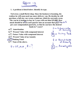


© Copyright 2026