ABC
docz
Explore
Log in
Create new account
Download
Report
No category
300 GHz microbolometer double-dipole antenna for focal
Marine and Land Based AM/FM Antenna
Product sheet
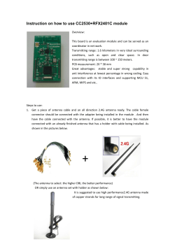
Instruction on how to use CC2530+RFX2401C module
Multi-beam Patch Antenna Design Mustafa Konca Supervisor: Prof. Dr. Sener Uysal
TCS Consultants, Inc. RF Coverage Site Data & Coverage Criteria Form
Coordinators ANTENNA THEORY & DESIGN
VQ4100 Quick Reference Guide
M i d S u s s e x M a t t e r s - Mid Sussex Amateur Radio Society
Quick start Guide Typical Use:
product brochure
© Copyright 2026
About abcdocz
DMCA / GDPR
Report