ABC
docz
Explore
Log in
Create new account
Download
Report
technology and computing
consumer electronics
Old Company Name in Catalogs and Other Documents
Old Company Name in Catalogs and Other Documents
How to Reboot/Shutdown Splicecom Maximiser 4140 Callserver
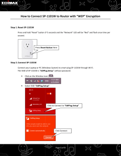
Edimax SP-1101W WEP Setup Guide
Business Plan
THE HOOK (AND PATTERN INTERRUPT)
How to upgrade your DualRunners ?
Sample Problem Set #2 - SOLUTIONS
APPLICATION NOTE R32C/100 Series Abstract Products
Awana Ministry Conference 2010 1
How to operate and set T100 series timer
© Copyright 2026
About abcdocz
DMCA / GDPR
Report