
Non-Destructive X-ray Characterization of Wide-Bandgap Semiconductor Materials and Device Structures
Non-Destructive X-ray Characterization of Wide-Bandgap Semiconductor Materials and
Device Structures
A dissertation submitted in partial fulfillment of the requirements for the degree of
Doctor of Philosophy at George Mason University
By
Nadeemullah A. Mahadik
Bachelor of Science
Old Dominion University, 2003
Director: Mulpuri V. Rao, Professor
Electrical and Computer Engineering
Fall Semester 2008
George Mason University
Fairfax, VA
Copyright: 2008 Nadeemullah A. Mahadik
All Rights Reserved
ii
DEDICATION
This work is dedicated to my parents, Mr. Anwar Ali Khan Mahadik and Mrs. Noorbanu
Anwar Mahadik for all the love and support, without which this work would not have
been possible.
iii
ACKNOWLEDGEMENTS
First and foremost, I would like to thank my advisors, Prof. Rao Mulpuri, and Prof. Syed
B. Qadri in their guidance and support throughout my graduate studies. I am grateful for
their encouragement to instill in me the drive to conduct research and solve fundamental
scientific problems.
I gratefully acknowledge the support from the following grants that made this work
possible: Army Research Office (Dr. Prater) under Grant # W911NF-04-1-0428, National
Science Foundation under Award # ECS-0618948.
Thanks are due to Dr. Siddharth Sundaresan (GeneSiC Semiconductor), Dr. Madhu
Gowda (GMU), Dr. Albert Davydov (NIST), Dr. Jaime Freitas (NRL), Dr. Abhishek
Motayed (NIST), Dr. Steven Binari (NRL), Dr. Michael Miller (NRL), Hany Issa
(GMU), and Geetha Aluri (GMU). Each has helped me greatly in this work.
I appreciate my dissertation committee members, Professors Dr. Mulpuri, Dr. Qadri, Dr.
Sutton, Dr. Berry, and Dr. Schreifels for their time and efforts in this work.
I would like to greatly thank my wife, Mrs. Fatma Cobb, my sisters, Mrs. Ghazala
Mahadik and Ms. Fazeela Mahadik, and my friends Mr. Mohammed Khaleeluddin and
Mr. Ayaz Sheikh for their love and support during my entire graduate studies.
iv
TABLE OF CONTENTS
Page
List of Tables………………………………………………………………………...….vi
List of Figures…………………………………………………………………….….....vii
Abstract.................................................................................................................……...ix
Introduction ......................................................................................................................1
X-ray Characterization Techniques ................................................................................11
Defects in Freestanding Gallium Nitride ........................................................................19
Lattice quality of Microwave Annealed Al ion-implanted SiC .....................................47
Microwave Annealed Mg-implanted GaN......................................................................61
Correlation of Strain and Bias in AlGaN/GaN Heterostructured Devices .....................75
Conclusions and Future Work ........................................................................................94
List of References………………………………………………………………………98
v
LIST OF TABLES
Table
Page
1. Material properties of SiC and GaN, in comparison with those of Si and GaAs ........3
2. The c and a lattice parameters, and the FWHM values
for HVPE grown GaN films ...........................................................................................25
3. Comparison of the rocking curve FWHM’s ωi, the normal, and lateral average grain
size as measured from the rocking curves and the HRXT images .................................39
4. FWHM’s of the (004) reflection of virgin, Al as-implanted and implanted/various
temperature annealed 4H-SiC ........................................................................................54
5. Calculation of the structure factor, |F|; penetration depth, ‘t’ and expected rocking
curve FWHM’s for the symmetrical reflections of 4H-SiC ...........................................57
6. Multiple energy Mg implantation schedule for GaN films ........................................63
7. c lattice parameters and rocking curve FWHM values of the multiple energy Mgimplanted 5 s microwave annealed GaN films ..............................................................65
8. a and c lattice parameters and FWHM values of the virgin, implanted and 15 s
microwave annealed GaN films .....................................................................................68
9. c lattice parameters and FWHM values of the 5 s annealed GaN films ....................69
vi
LIST OF FIGURES
Figure
Page
1. Rigaku ATX-E high resolution x-ray diffraction system at US Naval Research
Laboratory ......................................................................................................................14
2. Double crystal x-ray topography system at the US Naval Research Laboratory ......18
3. Experimental setup for GID measurement .................................................................21
4. 2θ / θ diffraction scan of Sample A HVPE GaN ........................................................24
5. GID spectra of Sample A at an angle of incidence 0.54o to the surface ....................27
6. The variation of the a-lattice parameter with the depth from the surface ...................27
7. The variation of FWHM with depth from the surface ................................................28
8. 71Ga NMR spectrum of Sample A oriented with
c-axis parallel to the magnetic field ................................................................................29
9. 71Ga NMR spectra of the left ST of Sample A oriented as in Fig. 8 ...........................31
10. Fully-relaxed 71Ga NMR spectra of the three GaN films .........................................33
11. High resolution double crystal x-ray topography arrangement ................................36
12. High resolution rocking curve for (006) GaN peak for Sample A ..........................38
13. HRXT image for Sample A using (104) reflection ...................................................40
14. HRXT image for Sample B using (104) reflection ...................................................41
15. HRXT image for Sample C using (104) reflection ...................................................42
16. Stationary HRXT measurements for measuring the sample warpage ......................44
17. 2θ/θ profiles for graphite capped SiC before and after 30s isochronal microwave
anneals at various temperatures ......................................................................................52
18. Narrow θ-2θ x-ray diffraction scan around the (0,0,4) reflection for the Al asimplanted 4H-SiC sample, showing the Kiessig fringes ................................................53
19. High resolution rocking curve using CuKα1 radiation for (004) SiC peak for the
virgin, as-implanted, conventional and microwave annealed samples ...........................54
20. Measured and expected FWHM values of the virgin and implanted/microwave
annealed sample as a function of increasing depth into the sample ...............................58
21. XRD spectra of the multiple energy Mg ion-implanted and microwave annealed
samples for 5 s duration ..................................................................................................64
22. XRD spectra of the 150 keV Mg ion-implanted and microwave annealed samples
for 15 s duration ..............................................................................................................66
23. GaN (004) XRD spectra of the microwave annealed 150 keV Mg ion-implanted
samples for 5 s duration ..................................................................................................67
24. Comparision of the x-ray rocking curve FWHM for implanted and 15 s
annealed GaN samples ....................................................................................................71
vii
25. Two-probe conductivity measurements on the single energy Mg-implanted, 15 s
microwave annealed samples ..........................................................................................72
26. Low-temperature PL spectra of virgin, as-implanted and microwave annealed
Mg-implanted GaN films ................................................................................................73
27. High resolution x-ray rocking curve (top) and high resolution x-ray diffraction
spectra (bottom) of GaN from AlGaN/GaN HEMT wafer .............................................80
28. Spatial distribution of the in-plane strain in GaN channel as measured by x-ray
diffraction on AlGaN/GaN HEMT wafer .......................................................................82
29. Spatial distribution of the electrical resistivity on the AlGaN/GaN HEMT wafer ...82
30. Forward I-V curve of the AlGaN/GaN Schottky diode ............................................85
31. High resolution x-ray rocking curve of GaN from AlGaN/GaN devices .................87
32. Change in the rocking curves positions with applied (a) forward and
(b) reverse bias for the GaN channel of the AlGaN/GaN Schottky diodes ....................88
33. The in-plane strain in the GaN channel with applied (a) forward bias, and
(b) reverse bias ................................................................................................................90
viii
ABSTRACT
NON-DESTRUCTIVE X-RAY CHARACTERIZATION OF WIDE-BANDGAP
SEMICONDUCTOR MATERIALS AND DEVICE STRUCTURES
Nadeemullah A. Mahadik, PhD
George Mason University, 2008
Dissertation Director: Prof. Mulpuri V. Rao
In this work non-destructive x-ray characterization techniques have been used to
study undoped and intentionally doped bulk and epitaxial layers, and device structures of
wide bandgap semiconductor materials, GaN and SiC. Novel non-destructive x-ray
characterization methods were developed to evaluate the uniformity of strain in
AlGaN/GaN device structures across the wafer and the results were correlated with
device electrical characteristics. In-situ bias induced strain measurements were also
carried out for the first time on the AlGaN/GaN Schottky diodes to estimate change in
piezoelectric polarization charge at the heterojunction interface with the gate bias voltage.
A variety of high resolution x-ray measurements were performed on freestanding
Gallium Nitride (GaN) films grown by three different laboratories using hydride phase
vapor epitaxy (HVPE) technique. The lattice parameters of the quasi-bulk films were
obtained using high-resolution x-ray diffraction spectra. The crystalline quality of the
films was determined by measuring the x-ray rocking curves and by
71
Ga nuclear
magnetic resonance (NMR) technique. The anisotropic in-plane strain was determined
using a novel grazing incidence x-ray diffraction technique (GID) and conventional x-ray
diffraction measurements. Based on these measurements the best free standing films have
surface strain anisotropy of 4.0791 x 10⁻³ up to a depth of 0.3 μm and the dislocation
density is in the range of 105-107 /cm2. High resolution x-ray topography (HRXT)
measurements were also performed on the freestanding GaN films. Complete mapping of
defects for the entire surface of the GaN films was obtained in a non-destructive way.
From these measurements, the lateral dimensions of crystallites and cavities in the films
are in the range, 200-500 nm, and 0.5-400 μm, respectively. The GaN films were found
to be warped with a radius of curvature of about 0.5 m. The warpage is attributed to
thermal mismatch between GaN and the sapphire substrate during growth. The
characteristics of freestanding GaN films measured in this work are detrimental to the
fabrication of high-speed devices such as high electron mobility transistors (HEMT)
because their performance is highly dependent on the surface and interface quality.
High resolution x-ray measurements were also performed on Al+ ion-implanted
4H-Silicon Carbide (SiC) epitaxial layers, before and after 30s ultra-fast microwave
annealing in the temperature range 1750-1900 oC, to examine the crystalline quality of
the material. Based on the FWHM values of the rocking curves, an improvement in the
crystalline quality of the microwave annealed samples was observed compared to the
conventional furnace annealed sample. The sample annealed at 1900 oC showed the best
rocking curve FWHM of 9 ± 2 arcsecs, which not only confirmed annihilation of the
defects introduced during the Al+ ion-implantation process, but also an improvement in
crystalline quality over the as-grown virgin 4H-SiC sample that had a rocking curve
FWHM of 18.7 ± 2 arcsecs. The theoretical and measured rocking curve FWHM values
were obtained and correlated with the depth dependent microwave absorption in the SiC
epilayer. These results are very significant for optimizing the annealing parameters to
achieve the highest possible implant activation, carrier mobility and crystal quality.
Magnesium ion-implantation doped GaN films were also characterized using xray diffraction measurements after microwave annealing in the temperature range of 1300
o
C – 1500 oC for 5 – 15 s. The FWHM values of the in-situ Mg-doped samples did not
change with the microwave annealing for 5 s anneals. The electrical measurements on
these samples also showed poor electrical activation of the Mg-implant in the GaN films.
These results may be due to the presence of a high concentration of implant generated
defects still remaining in the material, even after high temperature annealing for 5 s.
From the FWHM values, the 15 s annealing showed an improvement in the crystalline
quality of the GaN samples. Also the x-ray diffraction measurements show activation of
the Mg implant. Electrical conductivity was observed in these samples, which is due to
significant improvement in the crystalline quality and sufficient activation of the Mg
implant.
In this work, x-ray measurements were also performed on AlGaN/GaN device
structures to study the effect of localized strain on the transport measurements across the
wafer. The map of in-plane strain of the AlGaN/GaN HEMT wafer showed a one-to-one
correspondence with the variation in electrical resistivity. The in-plane strain variation is
in the range of 2.295x10⁻⁴ – 3.539x10⁻⁴ resulting in a sheet resistance variation of 345 411 Ω/.
The in-situ high resolution x-ray diffraction measurements, performed on the
AlGaN/GaN device structures under variable bias conditions, showed in-plane tensile
strain for forward bias conditions, and compressive strain for reverse bias. A linear
variation in the strain was observed with the bias voltage, which results in a change in the
piezoelectric charge at the AlGaN/GaN interface with bias. This variation needs to be
considered for the correct modeling of the device transport characteristics.
1. INTRODUCTION
1.1 Materials characteristics of gallium nitride and silicon carbide
High-power, high-frequency and opto-electronic applications like power
conversion, microwave and millimeter wave reception, blue light emission, etc. have
received much attention in the past decade. These applications are increasingly being
used in the telecommunication, transportation, aerospace, power transmission,
information storage, and various other industries. Wide bandgap materials offer
numerous benefits over silicon (Si) due to their favorable material properties. Advantages
of the wide bandgap materials over Si and gallium arsenide (GaAs) include:
1. Higher breakdown voltages (>1000 V) due to the larger breakdown electric field.
2. Better thermal conductivity, which results in easier cooling of the devices, and
consequently reliable device operation.
3. Unipolar devices like metal oxide semiconductor field effect transistors
(MOSFETs) fabricated in wide bandgap semiconductors have thinner depletion
regions and have lower on-state resistance, thus reducing conduction losses and
increasing the power efficiency. Thus, the disadvantages such as higher power
losses in Si-based bipolar devices like insulated gate bipolar transistors (IGBTs)
1
and PiN diodes can be avoided by replacing them with the wide-bandgap
semiconductor unipolar devices like MOSFETs and schottky diodes.
4. Wide bandgap semiconductor based devices also have lower switching losses due
to better reverse recovery properties. Hence, these devices can be operated at
higher frequencies.
The material properties of the two wide bandgap semiconductors of interest, namely
gallium nitride (GaN) and silicon carbide (SiC), in comparison with the traditional
semiconductors like Si and GaAs are given below in Table 1.
2 Table 1: Material properties of SiC and GaN, in comparison with those of Si and GaAs.
Si
GaAs
6H-SiC
4H-SiC
GaN
Bandgap (eV)
1.12
1.43
3.02
3.2
3.4
Breakdown field (kV/cm)
300
400
2500
2200
2000
Electron mobility (cm2/V.s)
1500
8500
500
1000
1200
Hole mobility (cm2/V.s)
600
400
100
115
850
Saturation velocity (cm/s)
1 x 10⁷ 1 x 10⁷ 2 x 10⁷
2 x 10⁷
2.2 x 10⁷
Thermal conductivity (W/cm.K)
1.5
4.9
1.3
0.46
3
4.9
The Gallium Nitride (GaN) is a wide bandgap material and has become very
important because of its potential electronic, optoelectronic, high-temperature, and highpower applications [1, 2]. GaN has a hexagonal wurtzite (α-GaN) structure with a direct
band gap of 3.4 eV. It also exists in a metastable cubic zinc-blende phase (β-GaN) having
a slightly lower band gap (3.2 eV). Due to its direct bandgap, GaN is very useful for
opto-electronic applications such as blue LEDs. Also, GaN has higher bandgap compared
to SiC, and higher carrier mobilities, hence GaN offers best performance in high
frequency devices. The GaN is also suitable for the growth of heterostructures using
AlxGa1-xN of variable Al concentration to fabricate high electron mobility transistors
(HEMTs). These HEMT structures exhibit very high electron mobilities (>1500 cm2/V.s)
due to quantum confinement of the electrons and the tunneling phenomena in the 2
dimensional electron gas (2DEG) at the AlGaN/GaN interface. These device structures
can be used for very high frequency (THz range) applications [3, 4]. Another attractive
feature of GaN is the possibility of inherent spontaneous and piezoelectric polarizationinduced three-dimensional doping [3, 4]. The strong piezoelectric effect and a large
spontaneous polarization allow for the incorporation of a large electric field (> 106 V/cm)
and a high sheet charge density (> 1013 cm-2) without any intentional doping. This
indicates a potential for fabrication of high-performance and high-power microwave
devices.
The SiC is another wide bandgap semiconductor material widely used for its
application in high-power, high temperature and high frequency devices, and also for its
chemically inert and diamond like characteristics [5]. The SiC has various polytypes of
4
which the 3C, 4H and the 6H polytypes are the most prominent. The 3C polytype has a
cubic zinc-blende type structure and has a much lower bandgap (~2.4 eV). The 6H and
the 4H-SiC polytypes have a wurtzite type hexagonal structure with higher bandgaps, 3
eV and 3.2 eV respectively. The fabrication of the 4H-SiC polytype needs precisely
controlled growth conditions and has been commercially available. This polytype has the
highest bandgap, and carrier mobilities among the SiC polytypes as seen from Table 1.
Also, the carrier mobilities are isotropic in all crystallographic directions for the 4H-SiC
whereas it is anisotropic for the 6H-SiC. Hence, the 4H polytype is more suited for the
high power devices.
1.2 Defects in gallium nitride and silicon carbide materials and devices
Gallium Nitride films are usually grown on substrates such as Al2O3, SiC, Si,
GaAs and MgO. These films are deposited on large substrates using some variation of
vapor-phase or molecular beam epitaxial growth. Due to mismatch of lattice parameters
and difference in coefficients of thermal expansion between GaN and its substrates, GaN
films are normally in a state of stress, which has a strong bearing on their opto-electronic
properties. None of the available substrates provide an excellent match for the
heteroepitaxial growth of GaN [6].
In order to reduce the number of defects found in GaN films grown on foreign
substrates, recently freestanding GaN films have been fabricated [7]. Thick layers of GaN
films are grown by hydride vapor phase epitaxy (HVPE) on sapphire substrates and then
lifted off. Since these films are pseudo-bulk, they are expected to have better crystalline
5
quality and fewer defects compared to the layers on mismatched substrates due to the
strain relaxation. Problems such as mismatch in coefficient of thermal expansion with the
substrate can also be avoided [7]. Although the freestanding GaN films are expected to
have better crystalline quality compared to the layers grown on SiC or sapphire
substrates, a lot of growth and surface treatment related defects may still exist in the films
due to the mismatched substrate used for the Hydride Vapor Phase Epitaxy (HVPE)
growth, even though the films are lifted off from the substrate. These structural defects
decrease the electron mobility [8], which is detrimental for high frequency devices; and
decrease the recombination lifetime, which results in poor luminescence [9, 10]. The
defects in the GaN films also result in generation of further defects in the heterostructures grown on the GaN material causing lowering of 2DEG mobility.
Silicon Carbide also faces several challenges in order to fabricate the planar high
power devices. One of these challenges is the inability to use diffusion for selective area
doping to form the necessary active and body regions of the device. This is because
thermal diffusion of most impurities into SiC is impractical even at temperatures in
excess of 1800 oC [11, 12]. Ion-implantation is the only known method to achieve
successful planar selective area doping [13, 14]. The ion-implantation process introduces
ions of the desired dopant species into the SiC samples at quite high energies (keV range)
causing significant lattice damage and introduction of defects, and also the dopant species
rest in the interstitial sites of the SiC lattice. In order to obtain the desired device
operation, the dopant species have to be electrically activated by driving them into
substitutional sites in the SiC lattice to either create a free electron or a hole, and also the
6
lattice damage has to be removed since the defects in the SiC will lower the carrier
mobility due to various defect scattering mechanisms.
1.3 Characterization of defects in gallium nitride and silicon carbide
High resolution x-ray diffraction (HRXRD) is a non-destructive technique that is
very useful in obtaining the precise lattice parameters, and defect information such as
strain distribution and misfit dislocation density in materials. Furthermore, spatially
resolved distribution of defects can be obtained with a length scale approaching a few
microns. The HRXRD measurements can also be used to observe any change in
crystalline symmetry in materials. It is also very useful to characterize the implanted
samples. Subsidiary peaks known as Kiessig fringes occur due to the interference of the
x-rays reflected from the top and bottom faces of the finite damaged layer. The absence
of these fringes in annealed material indicates removal of implant lattice damage. The
thickness of the implant layer can also be measured from the HRXRD measurements.
X-ray rocking curve measurement technique is also a non-destructive method to
evaluate the crystalline quality of the semiconductor materials. The full width at half
maximum (FWHM) of the high resolution rocking curves is a convolution of the
contributions arising due to random array of dislocations, particle size, strain and wafer
curvature [15]. This measurement provides a comprehensive measure of the crystalline
quality.
The high resolution x-ray diffraction and the rocking curve measurements can
also be modified to obtain localized lattice parameters, localized micro-strain, and the
7
crystalline quality from a region of the sample. Such measurements provide unique
opportunity to correlate lattice quality results with independently measured electrical
characteristics of the devices fabricated on the semiconductor materials. Furthermore, insitu characterization, using x-ray diffraction and rocking curve measurements, can also be
used to understand the physical phenomenon that takes place in the device structures
under variable bias conditions. These results are very helpful in developing accurate
models for device operation.
Double crystal high resolution x-ray topography analysis is a non-destructive
technique and is a very effective tool in evaluating the crystalline quality and its
uniformity across the wafer. Information on features such as average dislocation density,
surface defects and morphology, average strain, average crystallite sizes, detection of
stacking faults, voids or over-growths in the crystal can be obtained from these
measurements.
1.4 What is done in this work?
In this work, a variety of non-destructive x-ray characterization techniques were
used to study defects in Gallium nitride and Silicon Carbide. The virgin films,
doped/annealed films and the films after the complete device fabrication were
characterized and the results are analyzed in this work. The results are also correlated
with electrical characteristics of the devices.
Freestanding GaN films, grown using HVPE technique on c-plane sapphire and
separated from the substrate using laser lift-off process at three different laboratories,
8
were characterized for their lattice perfection. These films are considered quasi-bulk
because of the absence of the substrate, which results in a higher crystalline quality
compared to the films on the substrate. Defects introduced in the epilayers on the
substrate due to lattice mismatch and mismatch in thermal expansion coefficient can be
minimized in free standing layers separated from the substrates. Although the free
standing GaN films have lesser defects, surface polishing and the lift off process may
introduce some defects in these films. These defects are characterized using both
conventional high resolution x-ray diffraction and grazing angle x-ray diffraction
techniques for studying the dislocation density, and any strain in the material as a
function of increasing depth into the films. Furthermore, high resolution x-ray
topography was performed on these films to obtain a comprehensive mapping of defects
over the entire surface of the film. These measurements were performed for the first time
on free standing GaN films and provided important information on the nature of defects
in the films.
High resolution x-ray diffraction measurements were also performed on ion
implantation doped GaN films grown on sapphire substrate. These films were doped with
Mg+ to obtain p-type material, which is necessary for both high efficiency LEDs and
many high power devices. The x-ray diffraction and rocking curve measurements were
performed on the virgin, as-implanted and microwave annealed (1300 -1500 oC for 5-15
s) samples to study the crystalline quality and the defect density in these films.
Virgin, Al ion implanted and microwave annealed SiC films were analyzed using
high resolution x-ray diffraction and rocking curve measurements. The SiC films were
9
grown homoepitaxially on SiC substrates, and implanted with Al+ ions to obtain p-type
material. These films were annealed using the microwave annealing process in the
temperature range of 1700 -1900 oC for 30s. The x-ray measurements were performed to
study the crystalline quality and the defect density in these films. The depth of the
implant was checked using the Kiessig fringes obtained from high resolution x-ray
diffraction measurements. The annealing process was performed in order to activate the
implanted Al by moving them from interstitial sites to substitutional sites in the SiC
lattice and remove the defects in the SiC films caused by the implantation process. The
successful annealing schedules were determined by monitoring the rocking curve widths
and the sub-lattice peak intensities in the x-ray diffraction spectra.
The AlGaN/GaN device structures were characterized using conventional high
resolution x-ray diffraction, x-ray micro-diffraction, in-situ diffraction with variable
applied bias and high resolution rocking curve measurements. These studies were
performed in order to correlate the material characteristics of the AlGaN/GaN devices
with the electrical properties. These results are very helpful in improving the design,
processing conditions, and modeling of the devices.
10
2. X-RAY CHARACTERIZATION TECHNIQUES
In this chapter different non-destructive x-ray characterization techniques used in
this work are described. Details of novel x-ray arrangements used in this work are also
provided.
2.1 High resolution x-ray diffraction
X-rays were discovered in 1895 by Rontgen, who at that time did not know that
they were a form of electromagnetic radiation similar to light. These rays were
immediately put to use by medical professionals for x-ray radiography imaging, since
they could penetrate through less dense material like skin, muscle, and tissues. Using the
differing absorption of the x-rays by the dense bones and the less dense body material,
doctors could identify fracture or other anomalies in the body. At this time, the physical
properties of these electromagnetic x-rays were not understood. In 1912, the exact nature
of x-rays was found, and x-ray diffraction by crystals was discovered.
X-rays are produced when a metal target in vacuum is bombarded with an
electron beam above a certain critical power. The metal target produces x-rays of
characteristic wavelengths. These spectral lines fall into sets and are referred to as K, L,
and M lines. Usually, the K lines are used for x-ray diffraction measurements because
11
they are the most intense and also do not get absorbed easily. The x-rays are usually
monochromatized either by using elemental filters or by using a perfect crystal set at the
Bragg reflection to obtain the particular wavelength of x-rays.
High resolution x-ray diffraction is the only technique available to obtain the
precise lattice parameters, crystal orientation, and the phases of the material in a nondestructive manner. This technique is based on observing the scattered intensity of an Xray beam hitting a sample as a function of incident and scattered angle, polarization, and
wavelength or energy. When x-rays hit an atom, they either get absorbed with emission
of an electron or they cause the electrons in the atom to accelerate, which results in
scattered x-rays with the same frequency as the incident beam. This is known as Rayleigh
scattering. These scattered x-rays interfere with each other either constructively or
destructively, producing a diffraction pattern recorded by an x-ray detector. Since x-ray
wavelengths (λ ~ 1.5 Å) are comparable with inter-atomic distances (d-spacing) of most
atoms, they are an excellent match to find the inter-atomic spacing in materials.
The Bragg condition is met, resulting in diffraction, when the scattered x-rays
undergo mutually reinforcing constructive interference at a particular Bragg angle, θ, and
the d-spacing is then given by the Bragg’s law as:
λ = 2d sin θ
(1)
The diffraction happens due to the periodicity of atoms in a crystal lattice. When
the x-rays are scattered by the atoms of a crystal in phase with each other, their individual
amplitudes are summed together resulting in a diffracted beam. Hence, x-ray diffraction
can only be observed from materials having a crystalline symmetry. Materials lacking
12
this symmetry produce scattered radiation, which is not in phase and result in a weak
observable intensity. The intensity of the diffracted beam from crystalline materials can
be measured in a detector, which provides the Bragg angle of diffraction. The lattice
parameters of various materials can be obtained from their d-spacings obtained from the
Bragg angle of diffraction. The detailed derivation of the Bragg’s law can be found from
the original report of Bragg [16].
The x-ray diffraction system used in this work is a Rigaku ATX-E, high
resolution system, shown in figure 1. A high power (18kW) Cu rotating anode generator,
which produces much higher intensity compared to sealed tube generator, is used to
produce the incident x-rays. In this four crystal diffractometer, two channel cut Ge (220)
crystals are used to monochromatize the incident beam in order to obtain a pure Cu Kα1
(λ = 1.5405 Å) beam. A channel cut Ge (220) crystal can also be used to analyze the
diffracted beam from the sample. This arrangement removes the horizontal divergence of
the x-ray beam and provides accurate lattice parameters. The diffractometer also has an
open Eulerian cradle with independent χ (tilt), and φ (rotation) movements and an x, y, z
moving stage. This enables the user to align the sample perfectly. Additionally, in this xray diffraction system the maximum limit of the 2θ angle is greater than 155o, making the
measurement of lattice parameters highly accurate as given by the equation,
Δd
= −(cot θ )Δθ .
d
13
(2)
This equation is obtained by differentiating the Bragg law and simplifying it. Hence it
can be seen from this equation that as the Bragg angular separation, 2Δθ, becomes larger,
we get better resolution and more accurate lattice parameters.
Figure 1: Rigaku ATX-E high resolution x-ray diffraction system at US Naval Research
Laboratory.
14
2.2 High resolution x-ray rocking curve measurements
High resolution rocking curve measurements are performed on the same Rigaku
diffractometer, as shown in figure 1. After the sample is mounted, perfectly aligned, and
set at the Bragg diffraction angle, the single crystalline sample is rotated in the plane of
the x-ray beam, over a small angle. The x-ray reflection as a function of the rotation angle
is the rocking curve of the sample. The full width at half maximum (FWHM) of this
spectrum is a direct measure of the average dislocation density, thickness of thin films,
composition, and strain state of epitaxial single crystal films. The FWHM is broadened
by the contributions arising due to random array of dislocations, particle size, strain, and
wafer curvature. These individual effects can be decoupled by either taking multiple
reflections or by varying the wavelength of the incident x-ray beam. Since wide bandgap
semiconductors like GaN and SiC are epitaxially grown, defects such as dislocations play
an important role in the performance of these materials. Hence, the rocking curve
technique is very useful in characterizing the defects in these materials.
2.3 Double crystal x-ray topography
Double crystal (or high resolution) x-ray topography (HRXT) is a nondestructive
technique for imaging micrometer to centimeter sized defects in crystals using a
monochromatic incident x-ray beam. HRXT imaging can be done in two modes, either by
diffraction, where the diffracted image of the sample is measured, or transmission mode,
where the x-rays pass through the sample, and the image is obtained. In this work,
diffraction topography was used. The HRXT image provides a two-dimensional spatial
15
intensity map of reflected x-rays. This comprehensive mapping depicts the distribution of
scattering power from the crystal, revealing any defects in the lattice structure such as:
•
Dislocations or bundles of dislocations.
•
Crystal deformation and strain
•
Voids or inclusions in the crystal
•
Cracks and any surface scratches
•
Phase, Twin, or Grain boundaries
•
Non-crystalline areas of the wafer
•
Stacking faults
•
Growth striations, point defects or other defect clusters
In this technique, diffraction contrast mechanisms like structure factor, orientation
contrast and extinction contrast can be used. These contrast mechanisms are presented
below:
2.3.1 Structure factor contrast
The structure factor of a Bragg reflection is a mathematical description of the
intensity with which a crystal scatters the incident x-ray radiation. The diffracted
intensity is proportional to the square of the structure factor. The structure factor can be
calculated for most reflections of a particular phase of any crystalline material. Materials
with different structure factors will show different contrast in the HRXT image. Hence,
materials with twin phases or domains having different structures can be characterized
using this contrast mechanism.
16
2.3.2 Orientation contrast
If the material to be characterized has multiple crystallographic orientations, they
can be identified by this contrast mechanism. The aligned regions of the sample in the
Bragg condition will produce more intensity compared to the misaligned region. Multiple
HRXT images recorded with different Bragg conditions will show the multiple
crystallographic orientations in the sample. This contrast mechanism is useful in
characterizing materials, having a small variation in the orientation of neighboring
crystallites, especially observed in many epitaxial films.
2.3.3 Extinction contrast
This contrast mechanism is most useful in the characterization of defects such as
dislocations, point defects, strain, etc. It was first used by Lang [17] to observe
dislocations in a nearly perfect crystal, although the procedure followed was not a double
crystal arrangement. Extinction contrast can be explained using the dynamical scattering
theory. The diffracted beams are attenuated by both absorption and primary extinction in
perfect crystal regions, but are only attenuated by absorption in the areas surrounding a
defected region [18, 19]. Hence, the diffracted beam has higher intensity from the defect
regions. This results in a clear contrast in the HRXT image showing the defects.
The spatial resolution of the HRXT images is governed by the relation:
δ=
17
LV
,
D
(3)
where L is the distance of the photographic film to the sample, V is the fixed width of the
incident x-ray beam, and D is the distance of the sample from the x-ray source. For the
system used in this work, which is shown in figure 2, D is kept at 1.5 m in order to
minimize the vertical divergence of the incident beam, and the distance L is minimized in
order to get the smallest possible resolution. This system is capable of providing a
resolution of ~1 μm. Also, in this system, an asymmetrically cut (111) Si monochromator
is used, which is cut 1 o off the Bragg angle to provide a horizontal magnification of 26.
After exposure, the films are developed and digitized to analyze the results.
Figure 2: Double crystal x-ray topography system at the US Naval Research Laboratory.
18
3. Defects in Freestanding Gallium Nitride
Introduction
This Chapter deals with characterization of near surface defects in free standing
GaN films grown by a recently developed HVPE method.
Depth resolved x-ray
measurements and x-ray topography measurements were performed on freestanding GaN
films obtained from three different sources, to evaluate their quality. Grazing angle x-ray
diffraction as well as conventional x-ray diffraction measurements were also performed
on the films. The GaN films grown by HVPE technique on sapphire substrate were
subsequently separated from the sapphire substrate using laser lift off technique.
Although there have been numerous studies on the x-ray characterization of strain
in GaN films grown on sapphire substrates, not many reports exist on the evaluation of
free-standing GaN films. The process of surface polishing of such films generates
structural defects that may result in additional strain. These surface defects are
detrimental for device performance and may eventually lead to device failure. Grazing
incidence x-ray diffraction (GID) is used to measure the surface damage as a result of
mechanical and chemical processing of GaN films grown by hydride vapor phase epitaxy
(HVPE). In this novel technique, the x-ray beam is kept incident below the critical angle
to create an evanescent wave with finite penetration depth into the sample. The depth
19
dependant FWHM and in-plane lattice parameters are determined. In addition,
conventional HRXRD measurements are made to measure strain at greater depths. Also,
a new NMR spectroscopic approach was also applied to characterize the bulk GaN films
[20], relying on the sensitivity of
71
Ga NMR (I=3/2, 39.89% natural abundance) to
effects from conduction electrons [20, 21].
In addition to the depth resolved measurements, x-ray topography was performed
to obtain a complete mapping of defects in the GaN films. There have been a few reports
[22- 24] on investigating such defects in HVPE grown freestanding GaN, but there is no
comprehensive study on complete mapping of defects for the entire surface of the films in
a non-destructive way. Double crystal x-ray topography and high resolution rocking
curve measurements are non-destructive techniques and are very effective tools in
evaluating the crystalline quality. Information on features such as average dislocation
density, surface defects and morphology, average strain, average crystallite sizes,
detection of stacking faults, voids or over-growths in the crystal can be obtained from
these measurements.
The surface structure of freestanding GaN films is determined using the highresolution x-ray diffraction measurements. In addition, the possible origins of the defects
such as hexagonal cavities have been explained. In this work, the warpage and the
bending radius in the single crystalline freestanding GaN films is also investigated, which
results from the procedure of lifting off from the sapphire substrates.
20
3.1 Depth Resolved Determination of Surface Strain in Free Standing GaN Films
3.1.1 Experimental procedure
Unintentionally doped freestanding n-GaN films were used for this work. They
were epitaxially grown by hydride vapor phase epitaxy (HVPE) technique on (0001)
basal plane sapphire substrates and subsequently the substrates were removed. The x-ray
diffraction data was measured on an 18kW high-resolution Rigaku ATX-E four-circle
diffractometer using CuKα1 radiation. Rocking curves were also measured on the Rigaku
ATX-E diffractometer.
Grazing incidence angle (GID) diffraction normal to the (110) basal plane, was
performed to investigate the variation of the a-lattice parameter with depth as shown in
figure 3.
Figure 3: Experimental setup for GID measurement. ki is the incident x-ray beam, and kf
is the diffracted x-ray beam.
21
The angle of incidence of the x-ray beam to the surface was varied from 0.24o –
0.94o. The corresponding penetration depths into the surface of the HVPE GaN were
calculated using the X-Ray mass attenuation coefficient. A narrow beam of
monochromatic photons with an incident intensity Io, penetrating a layer of material with
mass thickness t and density ρ, emerges out with intensity I given by the exponential
attenuation law
⎡ μ ⎤
I = I o exp ⎢− t ⎥
⎣ ρ ⎦
(4)
where μ is the x-ray mass attenuation coefficient of the material for a given wavelength
of the incident x-ray beam. The attenuation coefficient can be computed from equation
(5) as:
μ=
ρ
⎛I ⎞
ln⎜ o ⎟
t ⎝ I ⎠
(5)
These coefficients have been computed and tabulated for all elements in a wide range of
energies. The attenuation coefficient for compounds, like GaN can be computed using the
summation by atomic weight percentages of the individual elements i and is given by the
relation,
μGaN = ρGaN∑mi (μi / ρi ) ,
(6)
i
Now the penetration depth of the x-rays for the GID measurement is computed as:
depth =
sin(θ i )
μGaN
22
(7)
Hence, the lattice parameters and the x-ray rocking curves of the GID peaks were
obtained to get a profile of the strain distribution at varying depths.
The
71
Ga static nuclear magnetic resonance (NMR) spectra were obtained at a
Larmor frequency of 152 MHz on a Bruker Avance DMX-500 NMR spectrometer. The
samples were placed in a high-power broadband probe equipped with a 7-turn flat coil
oriented so that the c-axis normal to the film, which coincides with the axis of the 71Ga
nuclear quadrupole coupling and chemical shift anisotropy tensors [20], could be aligned
at various angles with respect to the external magnetic field of 11.7 T. The NMR
measurements were performed by Dr. Yesinowski at the U.S. Naval Research
Laboratory.
3.1.2 Results and Discussion
Figure 4 shows an overlay of X-Ray diffraction scans of HVPE-grown GaN for
(00l) and (10l) reflections. The rocking curves were obtained for symmetric (002), (004)
and (006) reflections. The c-parameter was obtained from the specular (00l) reflections
using the relations,
d=
and
λ
2sinθ
,
c = d *l
23
(8)
(9)
(106)
(105)
(006)
(104)
200000
(004)
(002)
Intensity (arbitrary units)
250000
200000
150000
100000
50000
3000
2500
2000
1500
1000
500
300000
250000
200000
150000
100000
50000
250000
150000
100000
50000
0
20
40
60
80
100
2θ (degrees)
120
Figure 4: 2θ / θ diffraction scan of Sample A HVPE GaN
24
140
The Raleigh-Nelson correction was also applied to obtain the corrected value of c. The aparameter was obtained from the asymmetric (10l) reflections using the relation,
a =
1
⎛ 1
l
0 . 75 ⎜⎜ 2 − 2
c
⎝d
2
(10)
⎞
⎟⎟
⎠
The results, in Table 2, show that the c- and a- lattice parameters for all three samples are
similar to the GaN bulk values (c=5.1855 Å, a=3.189 Å) [25]. There is some variation in
the a-lattice parameter as a function of depth from the different (10l) planes, which
shows depth-resolved variation in strain. The epitaxial layers exhibit good crystalline
quality as determined by the narrow full width at half maximum (FWHM) of the rocking
curves.
Table 2: The c- and a-lattice parameters for HVPE GaN 2θ-θ reflection are given. The c-
parameter is the Raleigh-Nelson corrected value. ψ is the angle of incidence for the (104)
and the (106) reflections. Full width at half maximum (FWHM) of the rocking curves are
also specified.
Sample
c (Å)
(104)
a (Å)
(106)
ψ (deg)
(006) FWHM
a (Å)
ψ (deg)
(arc sec)
Sample A
5.1856
3.1861
17.015
3.1874
52.071
116.98
Sample B
5.1859
3.1980
15.24
3.1883
51.047
76.978
Sample C
5.1855
3.1828
15.629
3.1819
51.361
84.78
25
The results from the GID measurements show an expansion in the a-lattice
parameter as a function of depth and are tending towards the values obtained by
conventional HRXRD measurements for higher depths of 9-25 μm. Figure 5 shows the
diffraction pattern for an angle of incidence of 0.54o with the surface. The variation of the
a-lattice parameter with depth is shown in figure 6. It is observed that at a thickness less
than 0.3 μm the enlarged a-lattice parameter remains the same, giving an in-plane strain
anisotropy of 4.079 x 10⁻³ calculated using the relation:
a '− a 0
a0
26
(11)
Intensity (arb. units)
500
400
300
200
100
56.8
57.2
57.6
58.0
58.4
2θ (degrees)
Figure 5: GID spectra of Sample A at an angle of incidence 0.54o to the surface.
3.201
3.200
a (Å)
3.199
3.198
3.197
3.196
0.1
0.2
0.3
0.4
Depth (μm)
0.5
Figure 6: The variation of the a-lattice parameter with the depth from the surface.
27
The lattice parameter then decreases up to a thickness of 0.6 μm and relaxes to the
normal lattice parameter values at the higher depths as determined by the conventional
HRXRD measurements. The variation in strain as a function of depth is attributed to the
surface damage as a result of mechanical and chemical polishing and processing. The
FWHM of the rocking curves of the GID spectra are also shown in figure 7 as a function
of depth. The decrease in the average FWHM as a function of increasing depth also
suggests that the average strain relief occurs at greater depth, in agreement with the
lattice parameter measurements by conventional HRXRD. Similar general behavior of
lattice parameters and rocking curves was observed for the other two samples.
200
180
arc (s)
160
140
120
100
80
0.1
0.2
0.3
0.4
0.5
0.6
Depth (μm)
Figure 7: The variation of FWHM with depth from the surface.
28
The full
71
Ga NMR spectrum of Sample A is shown in Figure 8. A schematic
energy-level diagram is included for the four-level I=3/2
71
Ga spin in a high (Zeeman)
magnetic field and perturbed by a nuclear electric quadrupolar interaction (arising from
the presence of electric field gradients at the Ga sites) [26]. The central transition (CT)
between 1/2↔-1/2 levels occurs at a spectral position known as the “chemical shift”
(defined in “ppm” with respect to a reference compound); in highly-doped GaN samples,
an additional shift to high frequency known as the “Knight shift” arises from the
interaction of conduction electrons with the nucleus [20,21,26]. There are also two
satellite transitions (ST) between ±1/2↔±3/2 levels that give rise to a doublet, whose
splitting reflects the nuclear quadrupole coupling constant and hence electric field
gradient, and whose linewidths increase in the presence of any distribution of these
parameters due to defects.
Figure 8: 71Ga NMR spectrum of Sample A oriented with c-axis parallel to the magnetic
field.
29
A CT-selective saturation-recovery pulse sequence [27] was used to measure the
spin-lattice relaxation times T1 of the left and right CT peaks shown in the inset, with
resultant values of 0.34 s and 3.6 s respectively. This accords with the finding that the
Knight-shifted
71
Ga peaks in GaN have significantly shorter T1 values than the main
unshifted peak due to Korringa-type relaxation by conduction electrons, and correspond
to regions in the film with carrier concentrations above the Mott metal-insulator
transition.
Fig. 9 shows 71Ga spectra of the left (high-frequency) ST of Sample A, obtained
with a Hahn spin echo in order to reliably observe the broad peaks, for two different
values of relaxation delays, and the difference spectrum between the two spectra. The
difference spectrum (7c) shows that the more rapidly-relaxing broad component extends
over greater than a 100 kHz range (the true width may be broader but limited by the
excitation bandwidth of the echo sequence). Observation of similar behavior for the right
ST indicates that the broader ST component is associated with the rapidly-relaxing left
CT peak in Fig. 8 arising from a Knight shift. Similar two-component ST peaks have
been reported [20], and indicate that the regions of sample with high carrier
concentrations (and hence Knight shifts) also have a distribution of nuclear quadrupole
coupling constants and hence electric field gradients. Whether this distribution originates
from substitutional dopants such as oxygen or from other types of lattice defects is not
yet established.
30
Figure 9:
71
Ga NMR spectra of the left (high-frequency) ST of Sample A oriented as in
Fig. 8, obtained using a 90°-τ-180°-τ-Acquire Hahn spin-echo sequence
The half-height width of the fully-relaxed (long relaxation delay, i.e. quantitative)
71
Ga ST spectra for the three samples having a perpendicular c-axis orientation was
about 7.5 kHz for Samples A and C, and 8.7 kHz for Sample B, comparable to previous
values. It can be seen from Fig. 9c, a simple measurement is not very sensitive to
bimodal distributions with greatly differing linewidths, as might be anticipated for sample
B as well.
Figure 10 shows the fully-relaxed 71Ga NMR CT spectra of all three samples for
the perpendicular c-axis orientation. The differences in the chemical shift position of the
31
main peaks from those seen in Fig. 8 arise from a small chemical shift anisotropy and
second-order quadrupolar effects. The fact that the Knight-shifted left peak of Sample A
is still about 60 ppm to higher frequency from the main peak in this different orientation
(Fig. 8) implies that its chemical shift anisotropy (and quadrupole coupling) must be very
similar. Peak integration suggests that about 15% of the sample contributes to this
Knight shifted peak, which exhibits inhomogeneous broadening due to a distribution of
Knight shifts.
32
Figure 10: Fully-relaxed
71
Ga NMR spectra of three GaN film samples with c-axis
perpendicular to the magnetic field, recycle delay = 20 s, either 90° pulses (Samples A
and B) or Hahn spin-echo with delay interval = 40 μs (Sample C), line-broadening = 100
Hz. The slight 3 ppm shift to higher frequency of Sample C relative to the main peak in
other samples is of uncertain significance.
33
Similarly large Knight Shifts have been shown in polycrystalline GaN samples to
arise from degenerate electrons above the Mott transition, and the Knight shift
distributions analyzed to yield probability density functions for carrier concentrations, an
approach which could be applied here as well. A more intense Knight-shifted peak is
observed for Sample B. The
71
Ga spectrum of Sample C only has, in addition to the
major unperturbed GaN peak shown, a smaller shoulder to high-frequency with a shorter
T1 relaxation time (data not shown), suggesting also the existence of a much smaller
Knight shift effect.
These results show that HVPE GaN film samples can contain substantial portions
of the sample having much higher carrier concentrations that give rise to Knight-shifted
peaks, without such regions being evident in the lattice parameters or rocking curve width
measurements. Their inhomogeneous distribution makes characterization by electrical
measurements difficult, but Raman micro imaging has been successfully used to observe
carrier distributions in HVPE GaN films. It should also be possible to use spatiallylocalized
71
Ga NMR (either laterally or with vertical depth profiling) to observe the
spatial distribution of Knight-shifted peaks, and thus carrier concentrations.
34
3.2 Study of GaN freestanding films using double crystal x-ray topography
3.2.1 Experimental Details
High-resolution rocking curves were obtained using a triple axis four-circle
Rigaku ATX-E diffractometer. The HRXT measurements were taken using a double
crystal arrangement, as shown in figure 11, in which the distance between the source and
the first monochromating crystal was kept at 1.5 meters to minimize vertical divergence.
A Si (111) crystal, asymmetrically cut 1o off the Bragg reflection, was used to select
CuKα radiation and to provide a horizontal magnification for the incident x-ray beam.
The freestanding HVPE grown GaN samples were aligned in the (104) Bragg condition,
which is close to 90o with respect to the incident beam, allowing us to minimize the GaN
sample to the photographic film distance giving us the highest spatial resolution.
Because the GaN films were warped, only a small portion of the film diffracted at a time.
To obtain the full diffraction image of the sample, a modified Schwuttke technique [28]
was used. In this technique, the warped crystal is oscillated about its axis using external
computer control while the image is recorded on a stationary photographic film, which is
mounted parallel to the surface of crystal and at the closest possible distance to minimize
vertical divergence. Thus the high-resolution topographs of the entire films were
achieved by this new technique in a double crystal arrangement.
35
Figure 11: High resolution double crystal x-ray topography arrangement for imaging of
GaN films.
In addition to HRXT measurements in which the sample crystal was oscillating,
stationary HRXT images were taken to obtain the radius of curvature of the warpage in
the GaN crystals. These images were also taken using the similar double crystal
arrangement. The two stationary images were produced on a photographic film for a
fixed angular displacement of the GaN sample. The lateral displacement between the two
HRXT patterns was directly measured from the stationary images produced.
allowed us to calculate the radius of curvature for the warped film.
36
This
3.2.2 Results and Discussion
The rocking curves for the (00l) reflections of the freestanding GaN samples
were measured and their FWHMs (ωi) were between 60 and 88 arcseconds for the three
samples obtained from three different sources, indicating a reasonably good crystalline
quality. A representative rocking curve for Sample A taken for (006) reflection is shown
in Figure 12. Neglecting the contributions to the width of the rocking curves from finite
particle size, the upper limit of the average dislocation density is calculated using the
following equation [ 29- 31]
ρ=
ωi 2
4.35b 2
(12)
where, b (~5.1855 Å) is the length of the burgers vector, which is taken as equal to c-axis
lattice parameter [32]. Thus the upper limit of the dislocation density is estimated to be of
the order of ~107 lines/cm2 and is consistent with the topographs. The topographs tend to
show a uniform intensity distribution once the dislocations exceed 105 lines/cm2. Thus
the dislocation density can be between 105 – 107 lines/cm2. Similarly, assuming the
contribution to the width of the rocking curve only due to finite particle size, the lower
limit of the average crystallite size ‘t’ of the samples can be estimated using the Scherrer
equation [33]
t=
0.94λ
2ω i cos θ
(13)
where, θ (~60o) is the Bragg angle of the diffracting plane, and λ (=1.5405Å) is the
wavelength of the incident x-ray beam. The lower limit of the average crystallite sizes for
37
the GaN samples in the perpendicular direction were determined to be between 340-500
nm.
Figure 12: High resolution rocking curve for (006) GaN peak for Sample A
The HRXT images taken using (104) asymmetric reflections are shown in Figures
13 – 15 for the three GaN samples, and they reveal high dislocation densities based on
the FWHMs of the rocking curves. The average lateral dimensions of the crystallites were
obtained from the HRXT images, and are in the 200-500 nm range. The FWHMs of (006)
38
reflection and the average dimensions of the crystallites obtained from both rocking
curves and topographs are given in Table 3.
Table 3: Comparison of the rocking curve FWHM’s ωi, the normal, and the lateral
average grain size as measured from the rocking curves and the HRXT images.
Sample
Rocking curve FWHM
Normal crystallite size
Lateral crystallite size
A
60 arcsecs
500 nm
500 nm
B
70 arcsecs
427 nm
250 nm
C
88 arcsecs
340 nm
200 nm
In Figure 13, the HRXT image shows many surface features having dimensions in
the range of 300-1000 μm. These surface features emerge due to the damage induced by
post-fabrication surface polishing treatment. From the earlier GID studies we have found
that the surface damage is only at the surface and extends only to a depth of 0.5 to 0.6
μm.
39
1 mm
[104]
Figure 13: HRXT image for Sample A using (104) reflection. Surface features in the
order of 300-1000 μm are observed.
40
It can be seen from figures 14 and 15 that cavities and ridges are present in the
samples. The measured sizes of these cavities range from 0.5 to 400 μm. These defects
are observed for the first time by HRXT, and their origin is believed to be due to the
escape of nitrogen creating voids in the free standing GaN, as suggested by the TEM
work of Matsubara et. al. [34].
Figure 14: HRXT image for Sample B using (104) reflection. The surface is relatively
smooth. Small hexagonal cavities and ridges are observed.
41
Figure 15: HRXT image for Sample C using (104) reflection. The surface is marred with
ridges and large hexagonal cavities.
During the HVPE growth of GaN on sapphire, there is some nitrogen trapped by
dangling bonds between the GaN epilayers and the substrate. During the laser lift-off
process, it is possible that many of these dangling bonds are broken and nitrogen escapes
from the films. These voids have a hexagonal core as suggested by the TEM work and
such features are also observed in the HRXT images. Similar voids are also reported in an
earlier study [23] by Liliental-Weber et. al. Another defect observed in these samples is
the formation of ridges in the films with a periodicity of 2.375 mm and 1.66 mm,
respectively, in samples B and C. It can be observed that bundle of dislocations are either
42
originating or terminating at these ridges. These ridge formations are also believed to be
due to the effect of the laser lift-off process of the GaN films from the substrate used for
the HVPE growth, which may result in the desorption and re-deposition of the GaN at the
interface. This deformation may also produce numerous dislocations parallel to the
interface.
Furthermore, the topographic studies showed warpage in the films.
This
warpage is induced due to plastic deformation causing residual strain in the HVPE grown
GaN resulting from the large thermal expansion mismatch between sapphire and GaN at
the growth temperature of 1073K. Once the films are lifted off, the warpage sets in due to
this thermal expansion mismatch, although the GaN films are not warped originally on
the substrates. The radius of curvature r of the free-standing GaN samples can be
obtained from the stationary HRXT images as shown in figure 16. The displacement
l (~0.8 mm) in the image was measured as a function of angular displacement Δθ (~0.1o)
of the sample. Using the relation:
l = r Δθ
(14)
the radius of curvature was found to be of the order of 0.5 m. From the HRXT
measurements the sagittal radius s is computed, which quantifies the extent of bowing
from a flat sample surface, in the GaN samples using the expression:
s=
l Δθ
⋅
2 2
(15)
and was found to be ~0.35μm, which is significant to produce malfunctional devices,
particularly those that are fabricated in the wafer edges. The warpage induced after the
43
lift-off process in the GaN samples is thus detrimental to the fabrication and the yield of
operational devices from a single free-standing GaN wafer. Since large area (~300mm)
GaN wafers like silicon wafers are not commercially available, the effect of warpage in
the GaN samples is a huge concern that needs to be seriously considered for the
advancement in GaN wafer processing technology.
Figure 16: Stationary HRXT measurements showing the images after an angular
displacement of the sample to compute the radius of curvature for the sample warpage.
44
Summary of the results
The following conclusions can be drawn from the high-resolution x-ray diffraction,
grazing incidence diffraction (GID), high resolution x-ray topography and
71
Ga NMR
studies of the HVPE-grown freestanding GaN films:
(1) The a-lattice parameter shows an expansion up to a thickness of 0.6 μm, whereas
the c-axis lattice parameter is in agreement with the bulk GaN.
(2) Up to a thickness of 0.3 μm, the strain was of the order of 4.079 x 10⁻³. The
expansion in the lattice parameter is attributed to the defects and strain induced at
the surface due to mechanical and chemical polishing.
(3) The rocking curve measurements indicate the average strain distribution is due to
surface damage as a function of depth.
(4) Based on the topographs and the rocking curves the dislocation density is
estimated to be in the range of 105 – 107 lines/cm2.
(5) Surface features were found in the order of 300-1000 μm, and cavities of the
order of 0.5-400 μm were observed. The surface defects are due to the post grown
surface treatments, and the hexagonal cavities can be attributed to the escape of
trapped nitrogen leaving behind voids.
(6) The GaN samples are warped and have a radius of curvature in the order of 0.5m
as calculated from the HRXT measurements. This curvature is due to plastic
deformation and residual stress caused by a large thermal expansion mismatch
between the GaN film and the sapphire substrate at the growth temperature of
1073K. This curvature causes a bowing having a sagittal radius of ~0.35μm. The
45
wafer curvature may be detrimental to the fabrication and yield of devices made
from a single GaN freestanding wafer.
(7) A variety of 71Ga NMR measurements show, in addition to the peaks expected for
the highest purity c-plane GaN film sample studied by NMR6, broad and rapidly
relaxing high-frequency peaks in varying amounts for the three samples. These
additional peaks arise from Knight Shifts due to conduction electrons. They
reflect inhomogeneous distributions of carrier concentrations in the samples and
are associated with larger distributions of electric field gradients from defects.
(8) The high-resolution conventional and grazing incidence x-ray diffraction
measurements and the NMR studies provide complementary information about
the quality of the film.
46
4. Lattice Quality of Microwave Annealed Al Ion-Implanted
SiC
Introduction
In this work characterization of virgin, Al ion-implanted, and microwave annealed
Silicon Carbide (SiC) material has been carried out to establish the optimum annealing
parameters. Most of the devices like DMOSFETs, fabricated using the 4H-SiC polytype,
require selective area doping to create p-type and n-type regions, which can only be
achieved successfully by ion-implantation; but, the ion implantation process induces
lattice damage and the implanted ions introduced into the SiC lattice are located mostly in
the electrically inactive interstitial sites. Hence, post-implant annealing is required to
remove the lattice damage and also to electrically activate the implanted species.
Typically, annealing done in conventional furnaces is relatively long (~ 5-30
mins), which may cause the SiC surface to sublimate [35] and may also introduce some
new defects into the SiC sample. Ultra-rapid microwave heating technique [36] can be
used to anneal the implanted SiC samples at high temperatures (>1900 oC) for a short
time. Since, the microwave annealing is done for a much shorter duration (~ 30 sec),
compared to the conventional furnace annealing, the SiC surface sublimation and
diffusion of dopants and defects, which occur during the longer furnace annealing
47
process, can be avoided. The structural defects in SiC reduce the electron mobility and
hence lower the current density of the power devices. In order to study the average defect
density and to correlate the defect density with the annealing temperature, high resolution
rocking curve measurements were used in this work to evaluate the lattice quality of
microwave annealed SiC samples and to compare the results of the microwave annealing
with those of conventional annealing. The full width at half maximum (FWHM) of the
high resolution rocking curves is a convolution of the contributions arising due to random
array of dislocations, particle size, strain and wafer curvature.
It provides a
comprehensive measure of the crystalline quality.
In this work, the effectiveness of the microwave annealing technique is studied,
with respect to the conventional annealing, in restoring the crystalline quality of the ionimplanted SiC epilayers. It is shown how the crystalline quality at different depth
locations into the sample is affected by the new microwave annealing technique. Since,
the active device region in many device applications includes both the implanted and the
unimplanted regions, the effect of the microwave annealing on the crystalline quality of
both the regions is important for the device performance and reliability. Due to this
reason, the implanted region as well as the unimplanted region underneath the implanted
region was studied.
48
4.1 Effect of Microwave Annealing on Crystalline Quality of Al Ion-Implanted SiC
Epitaxial Layers
4.1.1 Experimental procedure
Lightly doped n-type (5 x 1016 cm-3), 6 μm thick, 4H-SiC epilayers, grown on
heavily doped n-type 4H-SiC substrates, which were cut 4o off axis from the normal
towards the [1120] direction, were used for this study. Multiple energy Al+ ion
implantation was performed at 500 oC to obtain a p-type implanted layer of ~0.3 μm
thickness. The multiple energy implantation schedules were designed to result in a
uniform Al concentration of 1.3 x 1020 cm-3. The implanted epilayers were spin-coated
with standard photoresist, heat treated in a furnace, and microwave heated at 1050 oC in
N2 ambient for 5s to form a graphite capping layer to protect the surface of the SiC
epilayers from possible sublimation during the microwave and conventional furnace
annealing processes. The graphite capped samples were microwave annealed in the
temperature range of 1750 – 1900 oC for 30s. For comparison conventional furnace
anneals were performed at 1800 oC for 5 min. Further details on the annealing procedure
are described elsewhere [37]. The graphite capping and annealings in this work were
done by Dr. Siddarth Sundaresan at George Mason University.
High resolution XRD measurements were taken on an 18kW Rigaku rotating
anode diffractometer using CuKα radiation. High-resolution rocking curves were
obtained using the triple axis four-circle Rigaku ATX-E diffractometer. The expected
FWHM values and penetration depths for the 4H-SiC samples were computed using the
49
dynamical scattering theory and Darwin treatment [38] for a perfect crystal. These values
were correlated with the measured FWHM values obtained from the high resolution x-ray
rocking curve measurements.
4.1.2 Results and Discussion
Figure 17 shows the (0,0,12) reflection XRD profiles for the graphite capped Alimplanted SiC epilayers before and after 30s isochronal microwave anneals at various
temperatures. The figure also shows the XRD profile for the conventionally annealed
(1800 oC/5 min) sample. All the diffraction profiles indicate very high crystalline quality
as evidenced from complete resolution of the Kα1 and the Kα2 components of the CuKα
radiation. Even in case of as-implanted sample the crystallinity remained because the
implants were performed at 500 oC. The lattice parameters were calculated using the
relation:
c = d *l ,
(16)
where d is the inter-atomic d-spacing and l is the Miller index and it is equal to 12 in
these measurements.
For the as-implanted sample, in addition to the SiC (0,0,12) reflection, sub-lattice
peaks (magnified 6 times) are observed on the low angle sides of the Bragg peak. These
peaks indicate the presence of a defect sub-lattice with larger d-spacing as compared to
the virgin sample caused by the implanted Al atoms occupying the interstitial lattice
positions. Additionally, subsidiary peaks also known as Kiessig fringes, shown in figure
18, appear between the main peak and the defect sub-lattice. This is due to the
50
interference of the x-rays reflected from the top and bottom faces of the finite Alimplanted SiC damaged layer. The thickness t of the implant layer can be calculated from
the equation
t=
λ
2(sin θ n − sin θ n −1 )
(17)
where, λ is the wavelength of the x-rays, θn and θn-1 are the Bragg angles of the nth and
the (n-1)th Kiessig fringe. The calculated thickness of the Al-implanted layer was found
to be 0.3μm, which correlates with the implantation profile from the SIMS measurements
(not shown). For all the annealed samples, the disappearance of the sub-lattice peaks (Fig.
17) indicates that the implanted species are incorporated into the lattice and that the
lattice damage due to implantation is removed.
51
Al+ implanted graphite capped SiC from Cree
o
1800 C Conventional Anneal
o
Intensity (arbitrary units)
Anneal 1900 C
o
Anneal 1850 C
o
Anneal 1750 C
As-implant
virgin
130.0 130.5 131.0 131.5 132.0 132.5 133.0 133.5 134.0 134.5 135.0
2θ (degrees)
Figure 17: 2θ/θ profiles for graphite capped SiC before and after 30s isochronal
microwave anneals at various temperatures.
52
Intensity (arbitrary units)
main (004)
peak
4
10 defect sublattice
peak
Kiessig fringes
3
10
2
10
1
10
35.3
35.4
35.5
35.6
2θ (º)
Figure 18: Narrow θ-2θ x-ray diffraction scan around the (0,0,4) reflection for the
Al as-implanted 4H-SiC sample, showing subsidiary peaks known as Kiessig fringes
between the defect sub-lattice peak and the main epilayer peak
Figure 19 shows the rocking curves for the (004) reflections of the virgin, asimplanted, conventionally annealed, and variable temperature microwave annealed 4HSiC samples. The FWHMs of the rocking curves, given in Table 4, show that the asgrown 4H-SiC virgin sample has a narrow rocking curve indicating excellent crystalline
quality.
53
High resolution rocking curves of 4H-SiC (004) reflection
Intensity (arbitrary units)
16000
14000
12000
10000
conventionally
annealed
o
1900 C
virgin
o
1850 C
as-implanted
8000
o
1750 C
6000
4000
2000
0
o
Δθ =0.03
Figure 19: High resolution rocking curve using CuKα1 (λ=1.5405 Å) radiation for (004)
SiC peak for the virgin, as-implanted, conventional and microwave annealed samples.
Table 4: FWHM’s of the high resolution rocking curves taken for the (004) reflection of
virgin, Al as-implanted and implanted/various temperature annealed 4H-SiC.
Sample
Virgin As-implanted Conv. Anneal
1750 oC
1850 oC
1900 oC
20.73
16.88
9.05
FWHM
(arcsecs)
18.71
41.35
34.11
54
After ion implantation, the FWHM increases due to the damage introduced by the
implanted species in the surface region (0.3 μm) of the material. Subsequently, the
microwave annealed samples showed a reduction in the FWHM for all the annealing
temperatures. Although the conventional annealing process was carried out at 1800 oC for
5 mins, there seems to be a very small reduction in the FWHM as compared with the
FWHM of the as-implanted sample. The electrical measurements also suggested that the
microwave annealed material has better properties (lower sheet resistance) compared to
the conventionally annealed material. Thus, the rocking curve FWHM values may
provide a quantitative measure on the effectiveness of the microwave annealing
technique in removing the implant lattice damage. Although, the conventional annealing
process is successful in activating the implanted species and consequently in generating a
sufficient number of carriers, a relatively high density of residual defects in the material
play a very significant role in lowering the carrier mobility. This is due to defect
scattering mechanisms, which affect the sheet resistance of the implanted 4H-SiC
samples by ~ one order of magnitude, as reported earlier [39]. The 1900 oC microwave
annealed sample shows a very low FWHM (9 ± 2 arcsecs) for the (004) SiC reflection,
which is lower than the FWHM of the virgin sample (18.7 ± 2 arcsecs), indicating that
the sample surface has a better crystalline quality than the virgin sample, and the
microwave annealing technique is effective in removing the epitaxial growth related
defects in the implanted region as well.
In order to study the crystalline quality as a function of depth, rocking curves
were obtained, on the virgin sample and implanted/1900 oC microwave annealed sample,
55
for higher order reflections. These results were compared with the expected FWHM and
the penetration depths calculated based on the dynamical theory of x-rays. The 4H-SiC
has a hexagonal structure with the P63mc (186) space group and two basis atoms in the
2a and 2b positions. The positions for the atoms are given as
0
0
⎧2 a 0
C⎨
⎩2b 1 / 3 − 1 / 3 0.25
0 3 / 16
⎧2 a 0
Si ⎨
⎩2b 1 / 3 1 / 3 7 / 16
and
The structure factor for a given reflection (hkl) is given as [40]
F (hkl ) = ∑ f r exp[2πi (hx r + ky r + l z r )]
(18)
r
where the summation is taken for all the atomic positions. After computing the structure
factors for all the required reflections for the 4H-SiC, the x-ray attenuation factor can be
computed as [38]
τ=
where,
π ⎛ e2 ⎞
⎟N λ F
⎜
2 ⎜⎝ mc 2 ⎟⎠
(19)
e2
= 2.82 x10 −13 , N is the atoms per cm3, λ is the wavelength of the x-rays,
2mc 2
and |F| is the average structure factor. Assuming the intensity attenuates as 1/e, the
penetration depth ‘t’ for a given reflection is given by,
t=
1
(20)
τ
The rocking curve FWHM (in arcsecs) for a particular reflection is calculated as [38],
s=
180 ⎛ e 2
×⎜
π ⎜⎝ mc 2
2
⎞ N λ F ⎛ 1 + cos(2θ )
⎜
⎟⎟
⎜
2
⎠ π sin(2θ ) ⎝
56
⎞
⎟
⎟
⎠
(21)
FWHM = 2.12 × s
(22)
where, θ is the angle of the particular Bragg reflection. The values for the structure
factors, expected FWHM, and penetration depths for the various symmetrical reflections
are given in Table 5. The as-grown virgin sample has higher FWHM values than the
expected FWHM for the (004) reflection, which shows the presence of growth-related
defects in the epilayer.
Table 5: Calculation of the structure factor, |F|; penetration depth, ‘t’; and expected
rocking curve FWHMs for the symmetrical reflections of 4H-SiC.
Expected FWHM
Reflection
|F|
d (Å)
θ
τ
t (μm)
(arcsecs)
(0,0,4)
41.32795
2.51325
0.3115
3428.91
2.92
7.29
(0,0,8)
21.06418
1.2566
0.6598
1747.66
5.72
3.08
(0,0,12)
22.20810
0.83775
1.16671
1842.57
5.43
5.88
After microwave annealing at 1900 oC, the FWHM values are comparable to the
expected FWHM values for the (004) reflection. Since, the devices to be fabricated will
have their active region within the top implanted layer of ~0.3 μm, and/or in the region
immediately under the implanted region, both the implanted region and the unimplanted
region underneath was probed. The expected penetration depth for the (004) reflection is
~3 μm, which is an order higher than the implanted region thickness. Hence, the above
57
results suggest that the novel microwave annealing process has not only removed the
implant generated defects, but also successfully produced a more desirable defect free
SiC epilayer. For comparison, the expected and measured FWHM values of various
symmetrical reflections are shown in fig. 20 for the virgin, and the 1900 oC microwave
annealed samples. From the FWHM values it can be seen that the lattice quality of the
top 3 μm of the implanted and annealed SiC epilayer has been significantly improved
after the microwave annealing.
Figure 20: Measured and expected FWHM values of the virgin sample and
implanted/microwave annealed sample as a function of increasing depth into the sample.
58
Also the FWHM of the rocking curves obtained from the reflections with greater
penetration depths have either same or better FWHM values for the microwave annealed
sample with respect to the virgin sample. This result can be explained by the fact that in
the microwave annealing technique, the conductivity of the sample plays an important
role in the absorption of the microwaves and consequently on the effective heating of the
sample [36]. Since, the sample is ion-implanted only at the surface, there is a
conductivity gradient across the epilayer thickness resulting in a more effective heating of
the surface region of the epilayer. This result shows that the microwave annealing
technique can be used successfully to obtain an implanted material having a very good
crystalline quality, and also to reduce defect concentration in the epitaxial layer in which
the implants are performed.
Summary of the results
High resolution x-ray rocking curve measurements (FWHM values of the rocking
curves) have been used to determine the crystalline quality of the virgin and ion
implanted 4H-SiC epilayers, before and after ultra-fast microwave annealing in the
temperature range of 1700 – 1900 oC. The microwave annealing technique is successful
in removing the lattice damage induced by the ion implantation process, and in activating
the implanted species in the 4H-SiC. The microwave annealing process also appears to
improve the crystalline quality of the epilayer region as compared to the virgin sample.
Since, the devices are fabricated using the implanted layer or the region just below it, the
microwave annealing appears to be a very promising technique for both activating the
59
implant and for significantly improving the crystalline quality of the entire epilayer,
which will result in an excellent device performance and reliability.
60
5. Microwave Annealed Mg-Implanted GaN
Introduction
In this Chapter, the feasibility of microwave annealing process for achieving Mgimplant activation in GaN films is studied using HRXRD and rocking curve
measurements. Using these results, the annealing parameters were optimized to obtain the
best crystalline quality and highest Mg implant activation in the GaN films for the first
time. Ion implantation is the only known selective doping method for GaN, since high
temperature thermal diffusion leads to incongruent evaporation of GaN, which leads to
creation of nitrogen vacancies. Ion-implantation also allows precise control of dopant
concentration and depth distribution. Since, as grown GaN is inherently n-type a much
higher implant activation of acceptor ions like Mg is necessary for realization of p-type
GaN material. Unfortunately, the high implant dose introduces lattice damage, and the
activated p-type carriers are easily trapped and compensated by the radiation defects,
resulting in less effective net acceptor activation [41]. Hence, high temperature (>1200
ºC) annealing is required for removing the implantation generated defects in GaN and
also to activate the Mg-implant. The GaN epilayers cannot withstand temperatures in
excess of 1100 ºC for more than a few seconds, due to low incongruent sublimation
temperature of N. Hence, to preserve surface morphology, the ramping rate to reach the
61
annealing temperature should be very fast, and the duration of the anneal should be
limited to few seconds [42, 43]. A novel ultra fast microwave annealing technique,
having a ramp rate of ~500 oC/s, was used to anneal the GaN samples in the temperature
range of 1300 – 1500 °C for 5 – 15 s durations. Additionally, the surface of the GaN
films was protected with an AlN capping layer deposited using pulsed laser deposition
technique.
5.1 Effect of Microwave Annealing on Crystalline Quality of Mg Ion-Implanted
GaN Epitaxial Layers
5.1.1 Experimental procedure
HVPE grown, 3 μm thick, GaN epilayers on sapphire substrates were obtained
from commercial sources. Single energy (150 keV) Mg-ion implantation was performed
at 500 oC to obtain a p-type implanted layer of ~0.2 μm thickness. The implantation
schedules were designed to result in a uniform Mg concentration of 5 x 1014 cm-3. A 0.6
μm thick AlN capping layer was deposited on the GaN films to protect the surface of the
epilayers from possible sublimation during the microwave annealing processes. The AlN
capped samples were microwave annealed in the temperature range of 1300 – 1500 oC,
for 5 – 15 s durations. The AlN capping layer was removed using chemical etching
before characterization.
For comparison, x-ray diffraction was also performed for microwave annealed
multiple energy Mg ion-implanted GaN films. The Mg ion-implantation was performed
at 500 oC, and the schedule is given in Table 6.
62
Table 6: Multiple energy Mg implantation schedule for GaN films
Implant Energy (keV)
Dosage (x1014 cm-2)
10
38
25
3.3
55
1.7
110
4.1
225
8.3
300
8.3
High-resolution x-ray diffraction and rocking curve measurements were
performed using the triple axis four-circle Rigaku ATX-E diffractometer. Symmetric and
asymmetric reflections were obtained to calculate both the a and c lattice parameters
before and after the microwave annealing process. The measured rocking curve FWHM
values were used to measure the crystalline quality of the samples.
Photoluminescence (PL) studies were performed using a He-Cd laser with an
excitation intensity of 2.5 mW to correlate with the HRXRD measurements. These
measurements were performed by Dr. Madhu Gowda at the US Naval Research
Laboratory.
63
5.1.2 Results and Discussion
Fig. 21 shows HRXRD spectra for the GaN (004) reflections on the as-implanted
and microwave annealed multiple energy Mg ion-implanted samples. It can be seen from
the HRXRD spectra that the sub-lattice defect peak for the annealed samples does not
disappear. This is due to the excessive damage produced by the multiple energy
implantation process in the GaN films, which cannot be reduced by the microwave
annealing process.
Figure 21: XRD spectra of the multiple energy Mg ion-implanted and the
microwave annealed samples for 5 s duration
64
The lattice parameters and rocking curve FWHM values for the multiple energy Mg
implanted GaN films are given in Table 7. From the FWHM values no significant
improvement is seen upon annealing of these samples. Due to the fact that the multiple
energy implantation process causes severe damage in the samples, single energy Mg ionimplantation was performed for further study of Mg acceptor activation in GaN.
Table 7: c lattice parameters and rocking curve FWHM values of the multiple energy
Mg-implanted 5 s microwave annealed GaN films.
Samples Reflection FWHM (arcsecs)
2θ (degrees)
c (Å)
as-imp
(004)
311.8
72.829
5.1903
1300 oC
(004)
309.5
72.785
5.1931
1400 oC
(004)
297.6
72.800
5.1921
Figures 22 and 23 show HRXRD spectra for the (004) reflections on the virgin,
as-implanted, and microwave annealed (15 s and 5 s, respectively) single energy Mg ionimplanted samples. The sub-lattice peak, which appeared in the as-implanted sample due
to the interstitial Mg atoms in the GaN lattice, disappeared after annealing. This shows
that the microwave annealing technique is successful in driving interstitial Mg atoms into
65
the substitutional positions. The lattice parameters were obtained from the HRXRD
measurements of the symmetric GaN (004) and asymmetric (104) reflections.
Figure 22: XRD spectra of the 150 keV Mg ion-implanted and the microwave annealed
samples for 15 s duration
66
Figure 23: GaN (004) XRD spectra of the microwave annealed 150 keV Mg ionimplanted samples for 5 s duration
The a, and c – parameters were computed using the equations,
c = d 004 × 4 ,
and
a =
⎡
⎤
⎥
4⎢
1
⎢
⎥
16 ⎥
3⎢ 1
− 2
⎢d2
c ⎥⎦
⎣ 104
67
(23)
(24)
The lattice parameters and rocking curve full width at half maximum (FWHM) values for
the virgin, as-implanted, and 15 s microwave annealed samples are given in Table 8.
Table 9 shows the c lattice parameters and FWHM values of the 5 s microwave annealed
samples.
Table 8: a and c lattice parameters and rocking curve FWHM values of the virgin,
implanted and 15 s microwave annealed GaN films.
Sample
Reflection
θ
Virgin
(004)
36.745
293.0
72.900
5.1860
(104)
16.918
209.1
82.040
3.1890
(004)
36.819
310.7
72.900
5.1860
(104)
16.741
231.5
82.027
3.1915
(004)
36.132
273.9
72.908
5.1855
(104)
15.545
197.6
82.036
3.1914
(004)
36.098
248.5
72.907
5.1856
(104)
15.508
206.8
82.035
3.1913
(004)
36.732
252.8
72.906
5.1857
(104)
16.879
207.9
82.038
3.1906
as implanted
1300 oC
1400 oC
1500 oC
FWHM (arcsecs) 2θ
68
c/a (Å)
Table 9: c lattice parameters and rocking curve FWHM values of the 5 s microwave
annealed GaN films.
Sample
Reflection FWHM (arcsecs)
2θ
c (Å)
1500 oC (004)
245.3
72.886 5.1869
1400 oC (004)
225.9
72.892 5.1865
1300 oC (004)
233.4
72.888 5.1867
The lattice parameters of the 15 s microwave annealed samples appear better compared to
the 5 s annealed samples. After annealing at 15 s, both the a, and c lattice parameters of
the GaN films are same as the values reported for bulk GaN material. This shows that the
microwave annealing at 15 s is very successful in removing strain in the GaN films. The
rocking curve measurements on the 5 s and 15 s annealed samples were performed at
different times and the system was reinitialized before the measurements in each case.
Hence, there is a possibility of small variation in the divergence present in the incident xray beam. This may cause the FWHM values to increase slightly. Hence, the FWHM
values of the 15 s and the 5 s annealed samples may vary slightly and can’t be compared.
For 5s annealing the lattice parameters show an expanded lattice and did not match with
the bulk GaN values even after 1500 C annealing. The FWHM values also did not show a
definitive improvement with increasing annealing temperature. This indicates that even
though the sub-lattice peak in the as-implanted sample disappeared a significant
concentration of defects still remains in the sample and are not annihilated by the 5 s
annealing. Two-probe electrical measurements on these samples did not show any
69
evidence of Mg electrical activation as in case of multiple energy Mg ion-implanted
samples. Based on the above results the annealing duration was extended from 5 s to 15 s.
Figure 24 shows the variation of the FWHM values of the implanted and 15 s
microwave annealed samples. It can be seen that the FWHM values decrease with
increasing annealing temperature till 1400 oC, and are same for both the 1400 oC and
1500 oC annealed samples. This shows an improvement in lattice quality and lower
dislocation density for the samples annealed at temperatures ≥ 1400 oC for 15 s.
Furthermore, from the FWHM values, the 1400 oC and 1500 oC 15 s annealed samples
also show a marginal improvement over the virgin sample, as observed before for ionimplanted SiC in the previous chapter . This shows that the microwave annealing process
is also successful in removal of the growth related defects.
70
Figure 24: Comparision of the x-ray rocking curve FWHM for implanted and 15 s
annealed GaN samples.
These results correlate well with two-probe conductivity measurements, shown in
fig. 25 on these films, which show that the 1400 C/ 15 s and 1500 oC/15 s microwave
annealed samples are conductive, whereas the samples annealed at lower temperature and
time are non-conductive. Hence, we observe that the 15 s microwave annealing of the
Mg-implanted samples at 1500 oC is successful in activating the Mg implant as well as
improve the crystalline quality of the GaN films. The net Mg acceptor activation stems
from the fact that the density of compensating donor defects in the lattice are effectively
decreased by the 15 s anneals for temperatures ≥ 1400 oC.
71
Figure 25: Two-probe conductivity measurements on the single energy Mg-implanted, 15
s microwave annealed samples.
Low-temperature PL, shown in Fig. 26, was performed on the virgin, implanted as
well as 15 s microwave annealed GaN films. The PL spectra shows an increase in Mg
activation for the 1300 ºC / 15 s annealed film by the presence of an intense Ultra violet
light (UVL) band at 3.29 eV zero phonon line (ZPL) as well as a relatively stronger nearband-edge emission (NBE) band at 3.46 eV with its phonon replica (1LO-NBE) at 3.37
eV. Upon increasing the annealing temperature to 1400 ºC/15s and 1500 ºC/15s, the
intensity of NBE band decreases with an increase in the intensity of broad near-UVL
band (2.7 – 3.1 eV). A broad yellow luminescence is also observed (2.0 –2.4 eV) in the
72
spectra of the annealed sample. An increase in the intensity and structure of the DonorAcceptor Pair (DAP) band with increasing temperature is also observed. These results
also correlate well with that of the HRXRD and two-probe electrical measurements, and
confirm the increase in the concentration of Mg acceptors at higher annealing
temperatures.
Figure 26: Low-temperature (5 K) PL spectra of virgin, as-implanted and microwave
annealed Mg-implanted GaN grown on sapphire; for 1300 ºC, 1400 ºC, and 1500 ºC. All
anneals were performed for 15 s.
73
Summary of the results
High resolution XRD and x-ray rocking curve measurements were used to
optimize the annealing parameters for achieving the best crystalline quality and highest
implant activation in Mg implanted GaN films. The crystalline quality was determined
for the virgin, as-implanted, and ultra-fast microwave annealed GaN epilayers in the
temperature range of 1300 – 1500 oC for 5 – 15 s durations. Based on the disappearance
of the sub-lattice peak in the HRXRD spectra and an improvement in the FWHM values,
the microwave annealing technique is found to be successful in removing the lattice
damage induced by the Mg ion implantation process, and in activating the implanted Mg
in the GaN films. This behavior, however, was observed only for single energy implanted
samples for an annealing temperature ≥ 1400 oC for a duration of 15 s. In case of multiple
energy Mg-implantation even 15 s annealing couldn’t result in any Mg activation due to
large degree of lattice damage, which introduces compensating donor levels. The
microwave annealing done at 1500 oC for 15 s also appears to improve the crystalline
quality of the epilayer below the implanted region as well. The crystalline quality and
percent of implant activation is very important in operation of the high power and high
frequency devices in the GaN films. Hence, optimized microwave annealing parameters
are necessary to realize fabrication of devices with excellent device performance and
reliability.
74
6. Correlation of Strain and Bias in AlGaN/GaN
Heterostructured devices
Introduction
This
Chapter
deals
with
the
characterization
of
Aluminum
Gallium
Nitride/Gallium Nitride (AlGaN/GaN) based devices. Recently, AlGaN/GaN high
electron mobility transistors (HEMT) have become important because of their potential
applications in electronic, optoelectronic, high-temperature, and high-power devices
[44,45]. AlGaN/GaN HEMTs have the desirable characteristics to replace GaAs based
power amplifiers due to the very high breakdown field of GaN which is estimated to be
3MV/cm [46]. However, heteroepitaxially grown GaN tends to have structural defects
arising due to mismatch in lattice parameters and, difference in coefficients of thermal
expansion between the GaN epilayers and the substrates such as silicon carbide or
sapphire.
Significant progress has been made in the fabrication and electrical
characterization of the HEMT devices [45,47- 50]. The AlGaN/GaN HEMT structures
have shown high electron mobility (>1500 cm2/V.s) resulting in low specific resistivity
values. However, for achieving more reliable device yields it is important to have
homogeneity in electrical transport properties across the entire wafer. To improve the
75
device performance and reliability, it is important to know the reasons for the variation in
the electrical properties across the wafer. In this work, the spatial variation of in-plane
strain in the GaN channel region of the HEMT devices is correlated with the variation in
device channel resistance across the wafer. The localized lattice parameters and rocking
curves at each point were measured to determine microscopic strain, crystalline quality
and dislocation density. These point-wise strain measurements were used for comparison
with the corresponding channel resistance measurements. Furthermore, these
measurements are benign to the overall device performance and are non-destructive in
nature. Hence, the x-ray micro-diffraction technique is unique in providing much needed
information on the range of variation in electrical characteristics of the HEMT devices on
the wafer even before the devices are made.
It has been known that both for zinc-blende semiconductors with a (111)
orientation [51] as well as for III-nitrides with a (0001) orientation [52] that piezoelectric
effects can vary the charge density and electric field distributions within these materials.
It has been shown that piezoelectric polarization in hexagonal AlGaN/GaN
heterostructures leads to an increase in the carrier concentration at the interface [53- 57].
In addition, pseudomorphically grown AlGaN/GaN layers have strain, which contributes
to a piezoelectric field at the interface. It has also been reported that due to this
polarization, the electron and hole wave functions are spatially separated in the
AlGaN/GaN quantum well thereby affecting the 2d electron gas (2DEG) [58].
Furthermore the polarization effects due to piezoelectric fields and other surface
states in AlGaN/GaN HEMT devices have been reported and correlated to the density of
76
the 2DEG [59,60]. They show a significant increase in the carrier concentration as a
result of increase in the strain induced piezoelectric charge at the AlGaN/GaN interface.
It has been found in these studies that both when the Al concentration is increased or
when the AlGaN layer thickness is increased the piezoelectric charge increases due to the
strain at the AlGaN/GaN interface. This was experimentally verified by measuring the
2DEG density as a function of the AlGaN layer thickness. The 2DEG density increases
initially due to an increase in the carrier concentration but starts to decrease later due to
an increase in carrier scattering effects.
Although the correlation of strain induced piezoelectric charges and carrier
concentration at the AlGaN/GaN interface has been studied, it is important to know the
variation in the strain with applied bias in these devices. This would provide further
insight into the 2DEG density in the GaN channel and the transport properties of the
AlGaN/GaN devices. In this work, the variation in strain due to the change in bias
applied to the AlGaN/GaN Schottky diodes was studied. Using in-situ high resolution xray micro-diffraction technique, the localized strain, and the respective rocking curves of
the GaN channel were obtained. This non-destructive technique is very useful because it
provides the bias dependant variation in the material parameters, within the active device
region. Additionally, the extrapolated piezoelectric charges from the strain measurements
were correlated with the bias applied to the device.
77
6.1 Surface Strain and its Impact on the Electrical Resistivity in GaN channel of
AlGaN/GaN HEMT
6.1.1 Experimental Procedure:
The AlGaN/GaN HEMT wafer was grown epitaxially on silicon carbide substrate.
A 0.1μm AlN nucleation layer was deposited followed by an unintentionally doped 1μm
GaN buffer/channel layer, and an undoped 250 Å Al0.25Ga0.75N layer. The devices were
fabricated using traditional photolithography and liftoff process. Ni/Au was used for the
Schottky gate metal and Ti/Al/Ni/Au was used for the ohmic contacts.
High resolution x-ray diffraction (HRXRD) and rocking curve measurements
were performed using the triple axis four-circle Rigaku ATX-E diffractometer. In order
to get the localized lattice parameters, strain, and the rocking curves from a specific
section of the wafer, incident beam slits were used to collimate the incident x-ray beam
and diffraction spectrum was obtained only from the required area on the sample. These
results from the specific regions of the wafer were then compared with the corresponding
electrical measurements.
The sheet resistance map was obtained by device I-V measurements across the
entire wafer.
78
6.1.2 Results and Discussion
Figure 27 shows a rocking curve measured for the (004) reflection of the GaN
channel in the HEMT device wafer. The FWHM value is ~200 arcseconds, suggesting
the dislocation density of ~1x10⁸ lines/cm2, which could be attributed to the strain arising
due to lattice mismatch of GaN with the substrate [61- 63]. The average crystallite size
was calculated to be ~ 100 nm from the Scherrer equation.
79
Figure 27: High resolution x-ray rocking curve (top) and high resolution x-ray diffraction
spectra (bottom) of GaN from AlGaN/GaN HEMT wafer.
80
The high resolution x-ray micro-diffraction measurements taken as a function of
the (x,y) coordinates on the (004) reflection of the GaN channel provide the spatial clattice parameters. The out of plane and the in-plane strain are computed using the
relations:
ε⊥ =
and
Δc
,
c
ε || = −νε ⊥ ,
(25)
(26)
where ε⊥ is the out of plane strain, ε|| is the in-plane strain, and (ν = 0.183) is the
poisson’s ratio of GaN [64]. The measured in-plane strain was in the range of 2.295x10⁻⁴
– 3.539x10⁻⁴ and the resistivity was in the range of 345 – 411 Ω/. The spatially resolved
in-plane strain is compared one-to-one with the resistivity measurements of the HEMT
devices on the wafer. Figure 28 and figure 29 show the spatial map of the in-plane strain
and the measured electrical resistivity, respectively. It can be seen from figures 28 and 29
that the variation in the in-plane strain correlates well with the variation in the electrical
resistivity of the sample. This result shows that the effect of tensile strain in the GaN
channel may result in a change of electrical resistivity.
81
Figure 28: Spatial distribution of the in-plane strain in GaN as measured by x-ray
diffraction on AlGaN/GaN HEMT wafer.
Figure 29: Spatial distribution of the sheet resistance on the AlGaN/GaN HEMT wafer.
82
It has been shown that the resistivity of semiconductor materials increases
exponentially with the increase in tensile strain [65]. The strain may be due to a
combination of different factors in the fabrication of the HEMT devices. The heteroepitaxial growth of the GaN channel region on the substrate, surface polishing, and
interfacial defects such as interface roughness between AlGaN and GaN may cause strain
in the GaN channel. Schottky gate metallization on AlGaN also contributes to the strain.
Non uniformities in AlGaN gate, the gate metal, GaN channel layer thickness can lead to
variation in strain across the wafer. If these measurements are performed on the samples
after growing each layer it is possible to find out cause for the major contribution of the
strain variation across the wafer. The non-destructive x-ray micro-diffraction
measurements of the lattice parameters provide a comprehensive analysis of the localized
strain. These results suggest that in order to have homogenous transport properties across
the wafer, the growth parameters of AlGaN layer, GaN channel, and the buffer layer have
to be optimized to reduce the strain and the strain variation across the wafer. This study
proves that x-ray micro-diffraction mapping is a useful tool in screening wafers for
achieving uniformity in electrical characteristics across the wafer. These unique
measurements can provide guidance in the fabrication of the AlGaN/GaN based devices
and on the areas to be improved and optimized in order to increase the wafer yield and in
improving the performance of the device.
83
6.2 In-situ Strain Measurements on GaN/AlGAN Hetrostructure Schottky Barrier
Diodes under Variable Bias Conditions
6.2.1 Experimental Procedure
The AlGaN/GaN samples were grown epitaxially on sapphire substrate using
metalorganic chemical vapor deposition (MOCVD) technique. An unintentionally doped
2μm thick GaN channel layer was grown followed by an undoped 250 Å Al0.25Ga0.75N
layer. The Schottky diodes were fabricated by lift-off lithography using Ni/Au
metallization. The diode structure consists of 115 µm diameter Schottky dots separated
from the field metal by exposed (lifted-off metal) ring areas. The separation between a
dot and the field metal area is 70 µm. The field metal surrounding the exposed ring
regions is considered as the body metal contact for the semiconductor. This structure
inherently has a high series resistance due to the field metal being on the AlGaN layer,
which results in a large forward voltage drop. The series resistance was measured from
the inverse slope of the linear segment of the forward I-V characteristics, shown in figure
30, and was found it to be ~ 2.7 kΩ.
84
Figure 30: Forward I-V curve of the AlGaN/GaN Schottky diode
High-resolution x-ray rocking curve measurements were made using the triple
axis four-circle Rigaku ATX-E diffractometer. In order to obtain the rocking curves from
the region of the device under bias, the incident beam slits were used to collimate the
incident x-ray beam to get diffraction only from the area of interest on the sample. X-ray
rocking curves were measured by varying bias conditions. Thus, the measured rocking
curves provide structural information on strain located in the device area under variable
bias conditions.
85
A Tektronix Type 576 Curve tracer was used to apply/measure the bias applied
in-situ during the high resolution x-ray measurements. Wire bonding was performed in
order to make contacts to the Schottky diode dots and the GaN body contact. Forward
bias was applied in the range of 0 to 10 V and reverse bias was applied in the range of 0
to -100 V. Large forward bias is the result of large series resistance between the
electrodes of the diode. The device under bias was allowed to settle for 10 s before
making the x-ray measurements.
6.2.3 Results and Discussion
Figure 31 shows a rocking curve measured for the (004) reflection of the GaN
channel under no bias condition. The FWHM value is ~300 arcseconds suggesting a
dislocation density of ~2x10⁸ lines/cm2 and this high dislocation density is attributed to
the strain arising due to lattice mismatch of GaN with the sapphire substrate and the
AlGaN/GaN interface [61]. The average crystallite size was calculated to be ~ 100 nm
from the Scherrer equation.
86
Fig. 31: High resolution x-ray rocking curve of GaN from AlGaN/GaN devices.
The Schottky diodes were forward biased in the range of 0 to 10V and reverse
biased in the range of 0 to -100V, and the corresponding in-situ x-ray rocking curves
were recorded as a function of variable bias. Figure 32 shows the rocking curves obtained
for various bias conditions of the GaN channel region. It can be seen from figure 32a that
on application of forward bias the peak position shifts towards the high-angle side
indicating an increase in the compressive strain in the perpendicular direction of the GaN
channel region, whereas application of reverse bias, as seen in figure 32b, causes an
opposite shift in the rocking curves, which reflects a tensile strain in the GaN channel.
87
The compressive to tensile shift in strain with bias polarity change is due to piezoelectric
behavior of AlGaN/GaN heterojunction.
Fig. 32: Change in the rocking curves positions with applied (a) forward and (b) reverse
bias for the GaN channel of the AlGaN/GaN Schottky diodes.
88
The out of plane strain, ε⊥ is computed using equation (27) and the in-plane strain
ε|| is related to ε⊥ by equation (28) [66]
ε⊥ = −
and
Δθ
,
tan θ
(27)
ε || = −νε ⊥ ,
(28)
where θ is the Bragg angle, and ν (= 0.183) is the poisson’s ratio for GaN. For the
forward bias measurements in the range of 0 to 10 V the in-plane strain variation was in
the range of 1.7x10⁻⁵ – 3.36x10⁻⁵, and for the reverse bias of 0 to -100V the strain
variation was in the range of -7.7x10⁻⁵ to -111.4x10⁻⁵. Figure 33 shows the variation of
the in-plane strain with forward and reverse bias. It can be seen from figure 33(a) that the
strain is positive, which reflects increasing tensile strain in the GaN channel, whereas in
figure 33(b) the strain is negative and decreasing, which means that a compressive strain
is developed in the GaN channel. Also in figure 33(b) a discontinuity is observed in the
strain after -50V, which is due to the depletion of the entire GaN layer causing
considerably high strain in the material. The depletion width with applied bias for a
Schottky diode is calculated using the relation:
⎡ 2ε (Vo − V ) 1 ⎤
W =⎢
⎥
q
Nd ⎦
⎣
1/ 2
,
(29)
where ε (= 8.41x10⁻¹³ F/cm) is the permittivity of GaN, q is the electric charge, and Nd
(~1016 /cm3) is the doping concentration. The depletion width for 50 V reverse bias is
calculated to be 2.2 μm, which is roughly the thickness of the GaN layer for this device
structure.
89
(a)
(b)
Fig. 33: The in-plane strain in the GaN channel with applied (a) forward bias, and (b)
reverse bias.
90
Using least square fitting the following equations were obtained for the in-plane strain:
For forward bias:
For reverse bias < 50V:
ε || = 1.3652 x10 −5 + 1.9715 x10 −6V
(30)
ε || = 3.1899 x10 −5 − 4.3545 x10 −6V
(31)
The piezoelectric polarization in a strained material can be computed using the relation
[60]:
PPE = e33ε ⊥ + 2e31ε ||
(32)
where e33 (=1 C/m2) [67] and e31 (= -0.49 C/m2) [68] are piezoelectric coefficients of
GaN. The AlGaN/GaN interface has much higher piezoelectric polarization compared to
other III-nitride semiconductor heterostructures even at zero bias due to strain at the
interface. In this study the strain relative to the strain at zero bias is measured for the
calculation of the piezoelectric polarization. Also, assuming that all the bias induced
strain may contribute to the piezoelectricity, the upper limit of the polarization field is
found to be in the range of -1.1x10⁻⁴ to -2.1x10⁻⁴ C/m2 for forward bias and 5x10⁻⁴ C/m2
to 12x10-4 C/m2 for reverse bias before the possible depletion of the entire GaN layer.
The maximum change in the sheet carrier concentration is calculated using the relation:
Δn s =
PPE
e
(33)
The change in the sheet carrier concentration with applied bias is found to be in the range
of 1010 to 1012 cm-2. This change in the sheet concentration is significant for reliable
91
of the strain in an operating AlGaN/GaN HEMT device on the effective 2DEG density
needs to be considered for an accurate device modeling.
Summary of the results
The high-resolution x-ray diffraction and rocking curve measurements were
performed on AlGaN/GaN HEMT devices as a function of (x, y) coordinates on the
wafer. Based on these measurements, the average dislocation density is estimated to be of
the order of 108 lines/cm2. The localized in-plane strain was found to be tensile in nature
for the GaN channel region of the AlGaN/GaN HEMT devices and in the range of
2.295x10⁻⁴ – 3.539x10⁻⁴. The corresponding electrical resistivities were in the range of
345 – 411 Ω/. The spatial map of the in-plane strain and the electrical resistivity map of
the wafer showed one-to-one correspondence. The origin of the in-plane tensile strain can
be attributed to a combination of different factors such as random array of dislocations,
surface polishing, lattice and thermal mismatch in the GaN channel/buffer region of the
HEMT device.
The high-resolution x-ray rocking curve measurements were performed in situ on
AlGaN/GaN Schottky diodes as a function of applied bias for the first time. The in-plane
strain for the GaN channel region of the AlGaN/GaN Schottky diodes as a function of the
applied forward and reverse bias was in the range of 1.7x10⁻⁵ – 3.36x10⁻⁵ for 0 to 10 V
forward bias and -7.7x10⁻⁵ to -111.4x10⁻⁵ for the reverse bias of 0 to -100V. The strain
was found to vary linearly with increasing bias, but there was a discontinuity in the strain
measurements for reverse bias greater than 50V due to possible depletion of the entire
92
GaN layer. The upper limit for piezoelectric polarization due to the bias induced strain is
calculated and found to be in the range of -1.1x10⁻⁴ to -2.1x10⁻⁴ C/m2 for forward bias
and 5x10⁻⁴ C/m2 to 12x10-4 C/m2 for reverse bias before the entire GaN layer is depleted.
This polarization causes a change in the sheet carrier concentration in the range of 1010 to
1012 cm-2, which may cause a variation in the 2DEG density in the GaN channel of the
AlGaN/GaN devices. The variation in the 2DEG density due to the bias induced strain
may result in unpredictable operation of the device and needs to be considered for the
correct modeling of the device transport characteristics.
93
7. CONCLUSIONS AND FUTURE WORK
7.1 Conclusions
In this work, the defects in wide bandgap semiconductor materials were studied
using non destructive characterization techniques. Novel x-ray characterization methods
were used for the first time in order to study the uniformity of strain in AlGaN/GaN
device structures across the wafer and the results were correlated with device electrical
characteristics. Additionally, bias induced strain in AlGaN/GaN Schottky diodes was
measured, and the results were correlated with the change in the piezoelectric charges at
the AlGaN/GaN interface. This phenomenon was studied for the first time, in this work.
Results of this work can be used in order to optimize the modeling and growth/processing
conditions of AlGaN/GaN devices.
Defects in freestanding GaN films were studied using high resolution x-ray
diffraction, grazing angle diffraction and x-ray topography. Anisotropic depth dependant
in-plane strain measured in these films was found to be 4.0791 x 10⁻³ up to a depth of 0.3
μm. High resolution x-ray topography studies provided a comprehensive map of defects
on the GaN films. The HRXT images showed presence of ridges, and cavities in these
films. Warpage was found in these films in the order of 0.5 m, which is detrimental to the
yield of devices fabricated on these films.
94
Virgin and Al ion-implanted 4H-SiC epitaxially grown films were characterized
using x-ray diffraction and rocking curve measurements to optimize the microwave
annealing parameters for best crystalline quality of the SiC films. Post implant
microwave annealed samples in the temperature range of 1700 oC – 1900 oC for 30 s
duration were used in this work. The x-ray diffraction measurement spectra show that the
microwave annealing process is successful in removing the lattice damage and in
activating the implant. From the FWHM values of the microwave annealed samples, it
can be seen that there is a significant improvement in the crystalline quality of the SiC
samples. The sample annealed at 1900 oC had the best rocking curve FWHM of 9 ± 2
arcsecs, which not only confirmed annihilation of the defects introduced during the Al+
ion-implantation process, but also an improvement in crystalline quality over the asgrown virgin 4H-SiC sample that had a rocking curve FWHM of 18.7 ± 2 arcsecs.
Single-energy Mg ion-implantation doped GaN films, characterized by using xray diffraction measurements after microwave annealing in the temperature range of 1300
o
C – 1500 oC for 15 s, showed activation of the Mg implant through the disappearance of
the sub-lattice peak observed in the as-implanted sample. From the rocking cuve FWHM
values, the 15 s annealing showed an improvement in the crystalline quality of the GaN
samples as compared to the as-implanted samples. Also electrical conductivity was
observed in these samples due to Mg implant activation.
The x-ray measurements performed on the AlGaN/GaN device structures show
the effect of localized strain on the sheet resistance across the wafer. The map of in-plane
strain in the AlGaN/GaN HEMT wafer was measured for the first time and it showed a
95
near one-to-one correspondence with the variation in device channel sheet resistance. The
in-plane strain variation is in the range of 2.295x10⁻⁴ – 3.539x10⁻⁴ resulting in a sheet
resistance variation of 345 - 411 Ω/.
The in-situ high resolution x-ray diffraction measurements, performed on the
AlGaN/GaN Schottky diodes under variable bias conditions, showed in-plane tensile
strain for forward bias conditions, and compressive strain for reverse bias. A linear
variation in the strain was observed with the bias voltage, which resulted in a change in
the piezoelectric charge in the range of -1.1x10⁻⁴ to -2.1x10⁻⁴ C/m2 for forward bias and
5x10⁻⁴ C/m2 to 12x10-4 C/m2 for reverse bias. The change in the sheet carrier
concentration with the applied bias was found to be in the range of 1010 to 1012 cm-2. This
variation needs to be considered for the correct modeling of the device transport
characteristics.
7.2 Future Work
It has been shown by in-situ x-ray diffraction, that the application of bias causes a
change in the piezoelectric charge at the AlGaN/GaN interface. This effect has to be
accounted for in the device models. Modeling parameters have to be developed in order
to account for the change in sheet carrier concentration of these devices with gate bias
voltage. Also, the relation of this effect to the current and power densities need to be
studied. The first step in order to perform this modeling, is to make similar measurements
on several high quality AlGaN/GaN device structures grown using different techniques.
The results have to be analyzed carefully and correlated with the applied bias. After
96
obtaining more results, the individual contributions of the interface strain such as the
piezoelectric effects, spontaneous polarization effects, etc. need to be identified. These
effects can then be added to the device models. Additional measurements such as in-situ
x-ray topography with variable bias at a synchrotron source should also be performed to
confirm these results.
The piezoelectric effect at the AlGaN/GaN interface is very high and can be used
for some novel applications. The effect of high pressure in this material is not studied and
may result in some unique findings. If sufficient strain is developed as a result of
application of high pressures, this might lead to creation of a piezoelectric charge at the
AlGaN/GaN interface and this charge in turn may yield current flow. High pressure x-ray
diffraction studies of this material in a diamond anvil cell should be carried out to find
this potential application.
With respect to acceptor implantation doping in GaN films, a detailed study
involving different doping concentrations need to be studied for developing ion
implantation conditions for efficient p-type doping.
97
LIST OF REFERENCES
98
LIST OF REFERENCES
[1] S. Nakamura, G. Fasol, The blue laser diode – GaN based light emitters and
lasers, Springer, Berlin, (1997)
[2] M. A. Kahn, M. S. Shur, J. N. Kuznia, Q. Chen, J. Burm, W. Schaff, Appl. Phys.
Lett. 63 (1993) 1214
[3] S.J. Pearton, C.R. Abernathy, F. Ren, Gallium Nitride Processing for Electronics,
Sensors, and Spintronics, Springer-Verlag, London (2006)
[4] Z. C. Feng (ed.), III-Nitride Semiconductor Materials, Imperial College Press.
London (2006)
[5] C.E. Weitzel, J.W. Palmour, A.H. Carter, K. Moore, K.K. Nordquist, S. Allen, C.
Thero, M. Bhatnagar, IEEE Trans. Electron Dev. 43 (1996) 1732
[6] T.D. Moustakas, T. Lei, R.J. Molnar, Physica B 185 (1993) 36
[7] Hermann M, Gogova D, Siche D, Schmidbauer M, Monemar B, Stutzmann M,
Eickhoff M, J. Crystal Growth 293 (2006) 462-468
[8] X.A. Cao, J.M. Teetsov, M.P. D’Evelyn, D.W. Merfeld, C.H. Yan, Appl. Phys.
Lett. 85 (2004) 7
[9] G. Franssen, S. Grzanka, R. Czernecki, T. Suski, L. Marona, T. Riemann, J.
Christen, H. Teisseyre, P. Valvin, P. Lefebvre, P. Perlin, M. Leszczynski, I.
Grzegory, J. Appl. Phys. 97 (2005) 103507
[10] M. Misheva, H. Larsson, D. Gogova, B. Monemar, Phys. Stat. Sol. (a) 202
(2005) 713
[11] S.C Singhal, J. Mater. Sci. 11 (1976) 1246
[12] G. Pensl, V. Afanasev, M. Bassler, M. Schadt, T. Troffer, J. Heindl, H. Strunk,
M. Maier, and W. Choyke, Inst. Phys. Conf. Ser. 142 (1996) 275
99
[13] J.B. Tucker, S. Mitra, N. Papanicolaou, A. Siripuram, M.V. Rao, O.W. Holland,
Diamond Relat. Mater 11 (2002) 392
[14] S-H. Ryu, S. Krishnaswami, M. O’Loughlin, J. Richmond, A. Agarwal, J.
Palmour, A.R. Hefner, IEEE Electron Device Lett. 25 (2004) 556
[15] M. J. Hordon, and B. L. Averbach, Acta Metall. 9 (1961) 237
[16] W.L. Bragg, Proceedings of the Cambridge Philosophical Society, 17 (1913), 43
[17] R. Lang, J. Appl. Phys. 30 (1959) 1748
[18] G.H. Schwuttke, Gen. Tel. Elec. Develop. J. 1 (1961) 68
[19] J. B. Newkirk, Trans. AIME 215 (1959) 483
[20] J.P. Yesinowski, phys. stat. sol. (c) 2 (2005) 2399
[21] Yesinowski, J.P.; Purdy, A.P.; Wu, H.; Spencer, M.G.; Hunting, J.; DiSalvo, F.J,
J. Am. Chem. Soc. March 2006
[22] T. Hashimoto, K. Fujito, F. Wu, B. A. Haskell, P. T. Fini, J. S. Speck and S.
Nakamura, Jpn. J. Appl. Phys. 44 (2005) L797
[23] Z. Liliental-Weber, Y. Chen, S. Ruvimov, and J. Washburn, Phys. Rev. Lett. 79
(1997) 2835
[24] F. A. Ponce, D. Cherns, W. T. Young, and J. W. Steeds, Appl. Phys. Lett. 69
(1996) 770
[25] H. Juza, Z. Anorg. Chem. 239 (1938) 285
[26] Slichter, C.P. Principles of Magnetic Resonance, 3d ed., Springer Series in
Solid-State Sciences, Springer-Verlag NY (1989)
[27] Yesinowski, J.P., J. Magn. Reson., 180 (2006) 147
[28] G. H. Schwuttke, J. Appl. Phys. 36 (1965) 2712
[29] P. Gay, P. B. Hirsch, and A. Kelly, Acta Metall. 1 (1953) 315
[30] M. J. Hordon, and B. L. Averbach, Acta Metall. 9 (1961) 247
[31] S. B. Qadri, and J. H. Dinan, Appl. Phys. Lett. 47 (1985) 1066
100
[32] J. Elsner, R. Jones, P. K. Sitch, V. D. Porezag, M. Elstner, and Th. Frauenheim,
M. I. Heggie, S. Öberg, and P. R. Briddon, Phys. Rev. Lett. 79 (1997) 3672
[33] P. Scherrer, Nachr. Gottingen, 2 (1918) 98
[34] T. Matsubara and K. Shoda, Jpn. J. Appl. Phys. 45 (2006) 279
[35] J. Senzaki, K. Fukuda, K. Arai, J. Appl. Phys. 94 (2003) 2942
[36] S. G. Sundaresan, M. V. Rao, Y. L. Tian, J. A. Schreifels, M. C. Wood, K. A.
Jones, A. V. Davydov, J. Elec. Mater. 36 (2007) 324
[37] S. G. Sundaresan, Y. L. Tian, J. A. Schreifiels, J. J. Kopanski, M. V. Rao, J.
Appl. Phys. 101 (2007) 073708
[38] B. E. Warren, X-ray Diffraction, Chap. 14 (1990)
[39] S. G. Sundaresan, Y. L. Tian, M. C. Ridgeway, N. A. Mahadik, S. B. Qadri, M.
V. Rao, Nuc. Inst. Meth. B 261 (2007) 616
[40] B. D. Culity, Elements of X-ray Diffraction (2001)
[41] C. Ronning et al. Phys. Reports 351 (2001) 349
[42] R.Y. Korotkov, J.M. Greigie, B.W. Wessels, Appl. Phys. Lett. 78 (2001) 222
[43] H.Y.A. Chung et al. J. Crys. Growth 230 (2001) 549
[44] U. K. Mishra, P. Parikh, and Y. F. Wu, Proceedings of the IEEE, 90 (2002) 1022
[45] G.H. Jessen, R.C. Fitch, J.K. Gillespie, G.D. Via, N.A. Moser, M.J. Yannuzzi, A.
Crespo, J.S. Sewell, R.W. Dettmer, T.J. Jenkins, R.F. Davis, J. Yang, M.A. Khan,
S.C. Binari, IEEE Elec. Dev. Lett. 24 (2003) 677
[46] V. A. Dmitriev, K.G. Irvine, C.H. Carter, N.I. Kuznetsov, E.V. Kalinina Appl.
Phys. Lett. 68 (1996) 229
[47] S.C. Binari K. Ikossi, J.A. Roussos, W. Kruppa, D. Park, H.B. Dietrich, D.D.
Koleske, A.E. Wickenden, R.L. Henry, IEEE Trans. Elec. Dev. 48 (2001) 465
[48] D.S. Katzer, S.C. Binari, D.F. Storm, J.A. Roussos, B.V. Shanabrook, E.R.
Glaser, Elec. Lett. 38, 1740 (2002)
101
[49] P.B. Klein, J.A. Mittereder, S.C. Binari, J.A. Roussos, D.S. Katzer, D.F. Strom,
Elec. Lett. 39 (2003) 1354
[50] A.P. Edwards, J.A. Mitereder, S.C. Binari, D.S. Katzer, D.F Storm, J.A.
Roussos, IEEE Elec. Dev. Lett. 26 (2005) 225
[51] E. A. Cardi, T. Y. Chang, K. W. Goosen, and L. F. Eastman, Appl. Phys. Lett. 56
(1990) 659
[52] W. Q. Chen, and S. K. Hark, J. Appl. Phys. 77 (1995) 5747
[53] Bykhovski, B. L. Gelmont, and M. S. Shur, J. Appl. Phys. 81 (1997) 6332
[54] P. M. Asbeck, E. T. Yu, S. S. Lau, G. J. Sullivan, J. Van Hove, and J. M.
Redwing, Elect. Lett., 33 (1997) 1230
[55] E. T. Yu, G. J. Sullivan, P. M. Asbeck, C. D. Wang, D. Qiao, and S. S. Lau,
Appl. Phys. Lett., 71 (1997) 2794
[56] M. B. Nardelli, K. Rapcewicz, and J. Bernholc, Appl. Phys. Lett 71 (1997) 3135
[57] T. Takeuchi, H. Takeuchi, S. Sota, H. Sakai, H. Amano, and I. Akasaki, Jpn. J.
Appl. Phys. Part 2, 36 (1997) L177
[58] Hangleiter, J. S. Im, H. Kollmer, S. Heppel, J. Off, and F. Scholz, MRS Internet
J. Nitride Sem. Res. 3 (1998) 15
[59] J. P. Ibbetson, P. T. Fini, K. D. Ness, S. P. DenBaars, J. S. Speck, and U. K.
Mishra, Appl. Phys. Lett. 77 (2000) 250
[60] O. Ambacher, J. Smart, J. R. Shealy, N. G. Weimann, K. Chu, M. Murphy, W. J.
Schaff, L. F. Eastman, R. Dimitrov, L. Wittmer, Stutzmann, W. Rieger, and J.
Hilsenbeck, J. Appl. Phys. 85 (1999) 3222
[61] P. Gay, P. B. Hirsch, and A. Kelly, Acta Cryst. 7 (1954) 41
[62] M. J. Hordon, and B. L. Averbach, Acta Metall. 6 (1958) 446
[63] S. B. Qadri, and J. H. Dinan, Appl. Phys. Lett. 47 (1985) 1066
[64] M.A. Moram, Z.H. Barber, C.J. Humphreys, J. Appl. Phys. 102 (2007) 23505
[65] R. Gosh, D. Basak, S. Fujihara, J. Appl. Phys. 96 (2004) 2689
102
[66] D. I. Ma, S. B. Qadri, M. C. Peckerar, and D. McCarthy, Thin Sol. Films, 206
(1991) 18
[67] G. D. O’Clock, and M. T. Duffy, Appl. Phys. Lett. 23 (1973) 55
[68] F. Bernardini, V. Fiorentini, and D. Vanderbilt, Phys. Rev. B 56 (1997) 10024
103
CURRICULUM VITAE
Nadeemullah Mahadik graduated with his Bachelors in electrical engineering from Old
Dominion University, Norfolk, Virginia in 2003. He worked at George Mason
University, Fairfax, Virginia as a graduate research assistant and conducted his research
at the US Naval Research Laboratory, Washington, DC and at the National Institute of
Standards and Technology, Gaithersburg, MD.
104


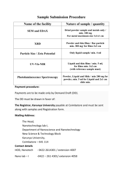

© Copyright 2026