
Reference Manual Tiger
Reference Manual DOC. REV. 1/23/2014 Tiger (VL-EPM-24) Intel Atom SBC with Ethernet, Video, USB, and PC/104-Plus interface WWW.VERSALOGIC.COM 12100 SW Tualatin Road Tualatin, OR 97062-7341 (503) 747-2261 Fax (971) 224-4708 Copyright © 2014 VersaLogic Corp. All rights reserved. Notice: Although every effort has been made to ensure this document is error-free, VersaLogic makes no representations or warranties with respect to this product and specifically disclaims any implied warranties of merchantability or fitness for any particular purpose. VersaLogic reserves the right to revise this product and associated documentation at any time without obligation to notify anyone of such changes. PC/104 and the PC/104 logo are trademarks of the PC/104 Consortium. VL-EPM-24 Reference Manual ii Product Release Notes Rev 1.00 – Commercial release. Support Page The VL-EPM-24 support page, at http://www.versalogic.com/private/tigersupport.asp, contains additional information and resources for this product including: Reference Manual (PDF format) Operating system information and software drivers Data sheets and manufacturers’ links for chips used in this product Photograph of the circuit board BIOS information and upgrades This is a private page for VL-EPM-24 users that can be accessed only by entering this address directly. It cannot be reached from the VersaLogic homepage. The VersaTech KnowledgeBase is an invaluable resource for resolving technical issues with your VersaLogic product. VersaTech KnowledgeBase VL-EPM-24 Reference Manual iii Contents Introduction ................................................................................................................... 1 Description.......................................................................................................................... 1 Features and Construction ..................................................................................... 1 Technical Specifications ..................................................................................................... 2 VL-EPM-24 Block Diagram ............................................................................................... 3 RoHS Compliance .............................................................................................................. 4 About RoHS........................................................................................................... 4 Warnings ............................................................................................................................. 4 Electrostatic Discharge .......................................................................................... 4 Lithium Battery...................................................................................................... 4 Handling Care ........................................................................................................ 5 Earth Ground Requirement .................................................................................... 5 Technical Support ............................................................................................................... 5 Repair Service........................................................................................................ 6 Configuration and Setup ............................................................................................... 7 Initial Configuration ........................................................................................................... 7 Basic Setup ......................................................................................................................... 7 CMOS Setup ....................................................................................................................... 9 Operating System Installation ............................................................................................. 9 Physical Details ........................................................................................................... 10 Dimensions and Mounting ................................................................................................ 10 VL-EPM-24 Dimensions ..................................................................................... 10 VL-CBR-5012 Dimensions ................................................................................. 11 Hardware Assembly............................................................................................. 12 Stack Arrangement Example ............................................................................... 12 External Connectors ......................................................................................................... 13 VL-EPM-24 Connector Locations – Top ............................................................ 13 VL-EPM-24 Connector Locations – Bottom ....................................................... 14 VL-EPM-24 Connector Functions and Interface Cables ..................................... 15 Connector Locations – VL-CBR-5012 ................................................................ 16 VL-CBR-5012 Connector Functions ................................................................... 16 Jumper Blocks .................................................................................................................. 17 Jumpers As-Shipped Configuration ..................................................................... 17 Jumper Summary ................................................................................................. 18 System Features .......................................................................................................... 19 Power Supply .................................................................................................................... 19 Power Connectors ................................................................................................ 19 Power Requirements ............................................................................................ 20 Power Delivery Considerations ........................................................................... 20 Power Cycling ..................................................................................................... 21 Lithium Battery.................................................................................................... 21 VL-EPM-24 Reference Manual iv Contents CPU................................................................................................................................... 21 System RAM..................................................................................................................... 21 CMOS RAM ..................................................................................................................... 22 Resetting CMOS and RTC .................................................................................. 22 CMOS Setup Defaults ...................................................................................................... 22 Default CMOS RAM Setup Values..................................................................... 22 Real Time Clock ............................................................................................................... 22 Setting the Clock.................................................................................................. 22 ACPI Power Management ................................................................................................ 23 S3 Sleep State ...................................................................................................... 23 Setup .................................................................................................................... 23 Entering Standby Mode ....................................................................................... 23 Wakeup ................................................................................................................ 24 Power Button Functionality ................................................................................. 24 Watchdog Timer ............................................................................................................... 25 Interfaces and Connectors ......................................................................................... 26 Ethernet Interface (J5) ...................................................................................................... 26 Ethernet Connector .............................................................................................. 26 Ethernet Status LEDs........................................................................................... 26 Video Interface (J11) ........................................................................................................ 27 Configuration ....................................................................................................... 27 LVDS Flat Panel Display Connector................................................................... 27 Compatible LVDS Panel Displays ...................................................................... 28 VGA Output......................................................................................................... 28 Console Redirection ............................................................................................ 29 IDE / PATA Interface (J3) ................................................................................................ 30 Loading Software onto a Disk on Module Device .............................................. 31 Main I/O Connector (J4) ................................................................................................... 32 Serial Ports ........................................................................................................................ 33 Serial (COM) Port Configuration ........................................................................ 33 Serial (COM) Port Connector Pin Functions....................................................... 34 USB Interface ................................................................................................................... 35 USB Client Mode ................................................................................................ 36 Programmable LED .......................................................................................................... 36 Internal Speaker ................................................................................................................ 36 Pushbutton Reset .............................................................................................................. 36 Audio ................................................................................................................................ 37 Expansion Buses ............................................................................................................... 37 PC/104-Plus (PCI + ISA) AND PCI-104 (PCI only).......................................... 37 PC/104 I/O Cycle Support ................................................................................... 38 PC/104 Memory Cycle Support ........................................................................... 38 IRQ Support ......................................................................................................... 38 DMA and Bus Master Support ............................................................................ 38 SPX Expansion Bus (J6)................................................................................................... 39 VersaLogic SPX Expansion Modules ................................................................. 39 SPI Registers ........................................................................................................ 40 System Resources and Maps ..................................................................................... 43 VL-EPM-24 Reference Manual v Contents Memory Map .................................................................................................................... 43 I/O Map ............................................................................................................................. 43 Interrupt Configuration ..................................................................................................... 44 Special Registers ........................................................................................................ 45 PLED and Product ID Register ......................................................................................... 45 Revision and Type Register .............................................................................................. 46 GPI Jumper Register ......................................................................................................... 47 Watchdog Timer Register ................................................................................................. 48 PC/104 I/O Block Enable Registers.................................................................................. 49 PC/104 Interrupt Request Enable Registers ..................................................................... 51 Appendix A – References............................................................................................ 53 VL-EPM-24 Reference Manual vi Introduction 1 Description FEATURES AND CONSTRUCTION The VL-EPM-24 is a feature-packed single board computer (SBC) designed for OEM control projects requiring fast processing and designed-in reliability and longevity (product lifespan). Its features include: Intel Atom processor Z530P, 1.6 GHz 533 MT/s FSB (standard temperature); Z520PT, 1.33 GHz, 533 MT/s FSB (extended temperature) Seven USB 2.0 ports (one client and six host) for keyboard, mouse, and other devices on two breakout boards TVS devices for ESD protection Up to 2 GB DDR2 memory, one SODIMM Intel High Definition Audio (HDA) compatible PATA Disk on Module, plugs directly into IDE connector SMSC hardware monitor Intel 82574IT-based Ethernet interface, autodetect 10Base-T / 100Base-TX / 1000Base-T Four RS-232/422/485 COM ports, 460 Kbps PC/104 compliant 4.49” x 3.78” footprint Field upgradeable BIOS with OEM enhancements ACPI 2.0 compatible Customization available PC/104-Plus (PCI + ISA) expansion IDE controller (ATA/ATAPI-6, UDMA 5, 100 MB/s), one channel, up to two devices LVDS flat panel display support The VL-EPM-24 is a single board computer (SBC) with an Intel Atom Z5xx (Menlow XL) processor. The board is compatible with popular operating systems such as Windows, Windows Embedded, Linux, VxWorks, and QNX. The VL-EPM-24 features high-reliability design and construction, including voltage sensing reset circuits and self-resetting fuses on the +5V supplies to the user I/O connectors. VL-EPM-24 boards are subjected to 100% functional testing and are backed by a limited twoyear warranty. Careful parts sourcing and US-based technical support ensure the highest possible quality, reliability, service, and product longevity for this exceptional SBC. The VL-EPM-24 is available with a multifunction utility cable (breakout board) that provides standard I/O connectors, including four COM ports, two USB host ports, one USB client port, and audio jacks. I/O expansion is available through the PC/104-Plus (PCI + ISA) and SPX connectors. VL-EPM-24 Reference Manual 1 Introduction Technical Specifications Specifications are typical at +25°C with +5V supply unless otherwise noted. Board Size: Audio: 4.49” x 3.78” (PC/104 compliant) Intel High Definition Audio compatible, stereo line in/out Storage Temperature: -40° to +85°C SPX: Supports four external SPI chips of user design or any SPX series expansion board Operating Temperature: VL-EPM-24SU: 0° to +60°C free air, no airflow VL-EPM-24EU: -40° to +60°C free air (100 LFPM from +60° to +85°C) Power Requirements: (with 2 GB RAM, Ethernet, keyboard, and mouse running Windows XP on a 3.5" PATA drive) +5V 5% VL-EPM-24SU: 1.20A (6.0W) typ./0.21A (1.1W) S3 VL-EPM-24EU: 1.18A (5.9W) typ./0.21A (1.1W) S3 +3.3V or ±12V may be required by some expansion modules System Reset: Watchdog timeout (warm/cold reset) Pushbutton reset ACPI: ACPI 2.0 compatible BIOS: Phoenix Technologies Embedded BIOS with OEM enhancements. Field reprogrammable. Support for USB boot. User-configurable CMOS defaults. Bus Speed: CPU FSB: 533 MT/s PCI: 2.5 Gbps LPC: 33.33 MHz ISA: 8.33 MHz Compatibility: PC/104-Plus – Partial compliance Weight: (no memory installed) DRAM: One SO-DIMM socket, 256 MB to 2 GB, DDR2, eight chips max. JEDEC raw card types A and C SO-DIMMs. Use VL-MM8 approved modules. VL-EPM-24SU – 0.265 lbs (0.120 kg) VL-EPM-24EU – 0.286 lbs (0.129 kg) Video Interface: Up to 1280 x 1024 (24 bits) @ 85 Hz LVDS output for TFT FPDs VGA output with VL-CBR-2010/12 cable and VLCBR-2014 adapter card IDE/PATA Interface: One channel, 44-pin, 2 mm connector. Supports up to and including ATA-6, UDMA/100 interface Supports two Parallel ATA IDE devices (hard drive, CD-ROM, CF, etc.) Flash Storage: 44-pin PATA Disk on Module (DOM). Shares IDE channel, master or slave Ethernet Interface: Intel 82574IT-based 10Base-T / 100Base-TX / 1000Base-T Ethernet controller COM1-4 Interface: RS-232/422/485, 16C550 compatible, 460 Kbps max., 4-wire RS-232 (only CTS and RTS handshaking) USB: Seven USB ports on two I/O connectors. One client and six host. Client and five host are 2.0/1.1 ports; one host port is 2.0 only. Client port can be configured as host in CMOS Setup. Specifications are subject to change without notification. VL-EPM-24 Reference Manual 2 Introduction VL-EPM-24 Block Diagram Intel Atom XL Processor PATA LVDS Video DDR2 SDRAM DDR2 SDRAM DDR2 SDRAM DDR2 SDRAM DDR2 SDRAM DDR2 SDRAM DDR2 SDRAM DDR2 FSB PATA / IDE DDR2 SDRAM SO-DIMM Intel HDA LVDS Intel System Controller Hub (SCH) Intel HD Audio Codec Audio Line In/Out (3) USB 1.1/2.0 PCI v2.3 PCIe Bridge PCIe x 1 PCI LPC (4) USB 1.1/2.0 USB3 1.1/2.0 USB4 1.1/2.0 USB5 1.1/2.0 USB6 2.0 USB2 1.1/2.0 Client Audio Line In Audio Line Out USB0 1.1/2.0 COM1 COM2 USB1 1.1/2.0 COM3 COM4 I/O Connector LPC Super I/O Serial I/O Connector LPC ISA Intel 82574IT Gigabit Ethernet MAC/PHY (CPLD) FWH LPC-to-PC/104 Bridge VersaRegs PC/104 SPI SS0/1/2/3 System Management Controller SPX SPX Controller Figure 1. System Block Diagram VL-EPM-24 Reference Manual 3 Introduction RoHS Compliance The VL-EPM-24 is RoHS compliant. ABOUT ROHS In 2003, the European Union issued Directive 2002/95/EC regarding the Restriction of the use of certain Hazardous Substances (RoHS) in electrical and electronic equipment. The RoHS directive requires producers of electrical and electronic equipment to reduce to acceptable levels the presence of six environmentally sensitive substances: lead, mercury, cadmium, hexavalent chromium, and the presence of polybrominated biphenyls (PBB) and polybrominated diphenyl ethers (PBDE) flame retardants, in certain electrical and electronic products sold in the European Union (EU) beginning July 1, 2006. VersaLogic Corp. is committed to supporting customers with high-quality products and services meeting the European Union’s RoHS directive. Warnings ELECTROSTATIC DISCHARGE Warning! Electrostatic discharge (ESD) can damage circuit boards, disk drives, and other components. The circuit board must only be handled at an ESD workstation. If an approved station is not available, some measure of protection can be provided by wearing a grounded antistatic wrist strap. Keep all plastic away from the board, and do not slide the board over any surface. After removing the board from its protective wrapper, place the board on a grounded, static-free surface, component side up. Use an antistatic foam pad if available. The board should also be protected inside a closed metallic antistatic envelope during shipment or storage. Note: The exterior coating on some metallic antistatic bags is sufficiently conductive to cause excessive battery drain if the bag comes in contact with the bottom side of the VL-EPM-24. LITHIUM BATTERY Warning! To prevent shorting, premature failure, or damage to the lithium battery, do not place the board on a conductive surface such as metal, black conductive foam, or the outside surface of a metalized ESD protective pouch. The lithium battery may explode if mistreated. Do not recharge, disassemble, or dispose of in fire. Dispose of used batteries promptly and in an environmentally suitable manner. VL-EPM-24 Reference Manual 4 Introduction HANDLING CARE Warning! Care must be taken not to touch the exposed circuitry with your fingers when handling the board. Though it will not damage the circuitry, it is possible that small amounts of oil or perspiration on the skin could have enough conductivity to cause the contents of CMOS RAM to become corrupted through careless handling, resulting in CMOS resetting to factory defaults. EARTH GROUND REQUIREMENT Warning! All mounting standoffs (four on PC/104 boards, eight on EBX and EPIC boards) should be connected to earth ground (chassis ground). This provides proper grounding for EMI purposes. Technical Support If you are unable to solve a problem after reading this manual, please visit the VL-EPM-24 product support web page below. The support page provides links to component datasheets, device drivers, and BIOS and PLD code updates. VL-EPM-24 Support Page http://www.versalogic.com/private/tigersupport.asp The VersaTech KnowledgeBase contains a wealth of technical information about VersaLogic products, along with product advisories. Click the link below to see all KnowledgeBase articles related to the VL-EPM-24. VersaTech KnowledgeBase If you have further questions, contact VersaLogic Technical Support at (503) 747-2261. VersaLogic support engineers are also available via e-mail at [email protected]. VL-EPM-24 Reference Manual 5 Introduction REPAIR SERVICE If your product requires service, you must obtain a Return Material Authorization (RMA) number by calling (503) 747-2261. Please provide the following information: Your name, the name of your company, your phone number, and e-mail address The name of a technician or engineer that can be contacted if any questions arise Quantity of items being returned The model and serial number (barcode) of each item A detailed description of the problem Steps you have taken to resolve or recreate the problem The return shipping address Warranty Repair All parts and labor charges are covered, including return shipping charges for UPS Ground delivery to United States addresses. Non-warranty Repair All non-warranty repairs are subject to diagnosis and labor charges, parts charges, and return shipping fees. Please specify the shipping method you prefer and provide a purchase order number for invoicing the repair. Note: VL-EPM-24 Reference Manual Please mark the RMA number clearly on the outside of the box before returning. 6 Configuration and Setup 2 Initial Configuration The following components are recommended for a typical development system with the VLEPM-24 computer: ATX power supply DDR2 memory module (see “System RAM”) LVDS display (or analog display with VL-CBR-2014 adapter card) Standard I/O breakout board (VL-CBR-5012) USB keyboard and mouse USB SSD or floppy disk drive (optional) IDE hard drive (optional) IDE CD-ROM drive (optional) The following VersaLogic cables are recommended: VL-CBR-2012 (24-bit, Hirose) or VL-CBR-2011 (18-bit, JAE) or VL-CBR-2010 (18-bit, Hirose) – LVDS adapter cable VL-CBR-4406 – IDE data cable VL-CBR-4405 – IDE adapter board, if you are using drives with 40-pin connectors VL-CBR-1008 – Power adapter cable You will also need an operating system (OS) installation CD-ROM. Basic Setup The following steps outline the procedure for setting up a typical development system. The VLEPM-24 should be handled at an ESD workstation or while wearing a grounded antistatic wrist strap. Before you begin, unpack the VL-EPM-24 and accessories. Verify that you received all the items you ordered. Inspect the system visually for any damage that may have occurred in shipping. Contact [email protected] immediately if any items are damaged or missing. Gather all the peripheral devices you plan to attach to the VL-EPM-24 and their interface and power cables. It is recommended that you attach standoffs to the board (see Hardware Assembly) to stabilize the board and make it easier to work with. Figure 2 shows a typical start-up configuration (using RoHS-compatible cables). VL-EPM-24 Reference Manual 7 Configuration and Setup USB Keyboard and USB Mouse LVDS J1 J4 J3 J4 VL-EPM-24 TIGER VL-CBR- 5012 J11 VL-CBR- 2012 or VL-CBR-2011 J9 VL-CBR- 4406 Hard Drive VL-CBR- 1008 ATX Power Supply CD-ROM Drive OS Installation CD-ROM Power to Drives Figure 2. Typical Start-up Configuration 1. Install Memory Insert the DDR2 DRAM module into the SO-DIMM socket J10 on the bottom side of the board and latch it into place. 2. Attach Cables and Peripherals Plug the LVDS cable VL-CBR-2012 or VL-CBR-2011 or VL-CBR-2010 into socket J11 on the bottom side of the board. Attach the cable to the LVDS display. (Note: You can attach an analog monitor to connector J11 using the VL-CBR-2014 adapter card.) Plug the breakout board VL-CBR-5012 into socket J4. Plug a USB keyboard and USB mouse into socket J1 of the breakout board. (Note: In DOS, input is through a keyboard only. Due to a limitation of the BIOS, mouse function is not supported in DOS.) Plug the hard drive data cable VL-CBR-4406 into socket J3. Attach a hard drive and CDROM drive to the connectors on the cable. If the hard drive is 3.5”, use the 2 mm to 0.1” adapter VL-CBR-4405 to attach the IDE cable. Attach an ATX power cable to any 3.5” drive (hard drive or CD-ROM drive). VL-EPM-24 Reference Manual 8 Configuration and Setup Set the hard drive jumper for master device operation and the CD-ROM drive jumper for slave device operation. 3. Attach Power Plug the power adapter cable VL-CBR-1008 into socket J9. Attach the motherboard connector of the ATX power supply to the adapter. 4. Review Configuration Before you power up the system, double check all the connections. Make sure all cables are oriented correctly and that adequate power will be supplied to the VL-EPM-24 and peripheral devices. 5. Power On Turn on the ATX power supply and the video monitor. If the system is correctly configured, a video signal should be present. 6. Select a Boot Drive During startup, press the CTRL-B key to display the boot menu. Insert the OS installation CD in the CD-ROM drive and select to boot from the CD-ROM drive. 7. Install Operating System Install the OS according to the instructions provided by the OS manufacturer. (See Operating System Installation.) Note: If you intend to operate the VL-EPM-24 under Windows XP or Windows XP Embedded, be sure to use Service Pack 3 (SP3) for full support of the latest device features. CMOS Setup See VersaLogic Knowledgebase article VT1666 - VL-EPM-24 CMOS Setup Reference for complete information on CMOS Setup parameters. Operating System Installation The standard PC architecture used on the VL-EPM-24 makes the installation and use of most of the standard x86-based operating systems very simple. The operating systems listed on the VersaLogic OS Compatibility Chart use the standard installation procedures provided by the maker of the OS. Special optimized hardware drivers for a particular OS, or a link to the drivers, are available at the VL-EPM-24 Product Support web page at http://www.versalogic.com/private/tigersupport.asp. VL-EPM-24 Reference Manual 9 3 Physical Details Dimensions and Mounting VL-EPM-24 DIMENSIONS 3.050 + + 3.350 0.150 The VL-EPM-24 complies with PC/104-Plus dimensional standards. Dimensions are given below to help with pre-production planning and layout. 3.575 3.375 3.250 3.175 0.125 DIA x4 Use 3mm or #4 standoffs J5 0.11 0.200 + J9 0.38 3.820 –0.200 0.000 -0.670 + 3.150 3.350 0.125 0.000 -0.200 Figure 3. VL-EPM-24 Dimensions and Mounting Holes (Not to scale. All dimensions in inches.) VL-EPM-24 Reference Manual 10 Physical Details 0.45 0.44 0.06 Figure 4. VL-EPM-24 Height Dimensions (Not to scale. All dimensions in inches.) VL-CBR-5012 DIMENSIONS 5.50 5.10 1.57 1.17 1.95 1.24 0.065 Figure 5. VL-CBR-5012 Dimensions and Mounting Holes (Not to scale. All dimensions in inches.) VL-EPM-24 Reference Manual 11 Physical Details HARDWARE ASSEMBLY The VL-EPM-24 provides both ISA and PCI connectors for adding expansion modules to the top and bottom of the stack. PC/104 (ISA only) modules must not be positioned between the VLEPM-24 and any PC/104-Plus (PCI + ISA) or PCI-104 (PCI only) modules on the stack. The entire assembly can sit on a table top or be secured to a base plate. When bolting the unit down, make sure to secure all four standoffs to the mounting surface to prevent circuit board flexing. Standoffs are secured to the top circuit board using four pan head screws. See page 10 for dimensional details. Standoffs and screws are available as part number VL-HDW-105. An extractor tool is available (part number VL-HDW-201) to separate the expansion modules from the stack. Use caution when using the extractor tool not to damage any board components. STACK ARRANGEMENT EXAMPLE Figure 6. Stack Arrangement Example VL-EPM-24 Reference Manual 12 Physical Details External Connectors VL-EPM-24 CONNECTOR LOCATIONS – TOP J4 COM1-4, USB 0-2, PLED, Speaker, Reset, Power Button, Audio line in/out J3 IDE J1 JTAG J2 PCI 1 2 J6 SPX J8 ISA J7 USB 3-6 15 16 J5 Ethernet J9 Power 2 1 10 9 = Pin 1 Figure 7. Connector Locations (Top) VL-EPM-24 Reference Manual 13 Physical Details VL-EPM-24 CONNECTOR LOCATIONS – BOTTOM J10 SO-DIMM J11 LVDS = Pin 1 Figure 8. Connector Locations (Bottom) VL-EPM-24 Reference Manual 14 Physical Details VL-EPM-24 CONNECTOR FUNCTIONS AND INTERFACE CABLES Table 1 provides information about the function, mating connectors, and transition cables for VL-EPM-24 connectors. Page numbers indicate where a detailed pinout or further information is available. Table 1: Connector Functions and Interface Cables Connector J1 J2 Transition Cable Mating Connector JTAG in-system programming PCI — — — 3.220 3.494 — AMP 1375799-1 FCI 89947-144LF — — 0.450 3.139 37 VL-CBR44062 12" 44-pin 2 mm latching / two 44-pin 2 mm 50-pin I/O cable to breakout board -0.258 1.211 30 -0.500 1.228 32 — 2 mm 14-pin IDC, 2 or 4 SPX device cable 0.024 0.523 26 — — 39 12" 2 mm 16-pin to 16pin IDC — Interface from standard ATX power supply — 3.120 0.504 35 0.050 0.298 0.200 -0.126 37 19 — — 21 — — 27 J3 IDE – HD, CDROM, or DOM J4 Main I/O – 4 COM, 2 USB host, 1 USB client, audio in/out, LED, speaker, power button, reset Gigabit Ethernet FCI 89361-350LF VL-CBR-5012 RJ45 SPX FCI 89361-714LF J7 USB 3-6 FCI 89361-716LF — VL-CBR-1401 or VL-CBR-1402 VL-CBR-1603 J8 J9 ISA Main Power Input — VL-CBR-1008 J10 SO-DIMM AMP 1375795-2 Berg 69176-010 (housing) + Berg 47715-000 (pins) DDR2 RAM J11 LVDS3 Molex 51146-2000 (housing) Molex 50641-8041 (pins) VL-CBR-2012 or VL-CBR-2010 or VL-CBR-2011 J5 J6 — Cable Description Pin 1 Location1 x coord. y coord. Function 24-bit TFT FPD using 20-pin Hirose conn. or 18-bit TFT FPD using 20-pin Hirose conn. or 18-bit TFT FPD using 20-pin JAE conn. 1. The PCB Origin is the mounting hole to the lower left. 2. VL-CBR-4405 44-pin to 40-pin adapter required to connect to 3.5" IDE drives with 40-pin connectors. 3. A VGA monitor can be connected to J11 using the VL-CBR-2014 LVDS to VGA adapter card. VL-EPM-24 Reference Manual 15 Page Physical Details CONNECTOR LOCATIONS – VL-CBR-5012 1 2 49 50 J5 COM3 J4 Paddle Board Adapter SP1 Speaker 5 5 1 J6 COM4 1 J2 COM1 (Top) COM2 (Bottom) J1 USB0 (Top) USB1 (Bottom) J7 USB2 J3 S1 D1 S2 Audio Power PLED Reset In (Top) (Top) Out (Bottom) Power LED (Bottom) Figure 9. VL-CBR-5012 Connector Locations VL-CBR-5012 CONNECTOR FUNCTIONS Table 2: VL-CBR-5012 Connector Functions and Interface Cables Connector J1 J2 J3 J4 J5 J6 J7 D1 S1 S2 SP1 Function PCB Connector Description USB0, USB1 COM1, COM2 Audio In/Out High Density Connector COM3 COM4 USB2 PLED (Top), Power LED (Bottom) Power Button Reset Button Speaker USB Type A Kycon K42-E9P/P-A4N 3.5 mm dual audio jack FCI 98414-F06-50ULF Conta-Clip 10250.4 Conta-Clip 10250.4 USB Type B LED Pushbutton Pushbutton Piezo speaker USB Host Dual DB-9 male – 2 mm, 50-pin, keyed header 5-pin screw terminal 5-pin screw terminal USB Client – – – – VL-EPM-24 Reference Manual 16 Physical Details Jumper Blocks JUMPERS AS-SHIPPED CONFIGURATION V1 2 8 V3 V2 4 6 1 1 2 3 1 2 3 4 7 Figure 10. Jumper Block Locations VL-EPM-24 Reference Manual 17 Physical Details JUMPER SUMMARY Table 3: Jumper Summary Jumper Block Description V1[1-2] COM1 Rx End-point Termination In – 120 Ohm termination active Out – No termination Places terminating resistor across COM1 RS-485 TXRX+/TXRX- or RS-422 RX+/RX- differential pair. Jumper must be out for RS-232 operation. V1[3-4] COM2 Rx End-point Termination In – 120 Ohm termination active Out – No termination Places terminating resistor across COM2 RS-485 TXRX+/TXRX- or RS-422 RX+/RX- differential pair. Jumper must be out for RS-232 operation. V1[5-6] COM3 Rx End-point Termination As Shipped Out (Rev. 1.01 and later) Page 33 In (Rev. 1.00) Out (Rev. 1.01 and later) 33 In (Rev. 1.00) In 33 In 33 [1-2] In 22 In 47 In 47 In – 120 Ohm termination active Out – No termination Places terminating resistor across COM3 RS-485 TXRX+/TXRX- or RS-422 RX+/RX- differential pair. Jumper must be out for RS-232 operation. V1[7-8] COM4 Rx End-point Termination In – 120 Ohm termination active Out – No termination Places terminating resistor across COM4 RS-485 TXRX+/TXRX- or RS-422 RX+/RX- differential pair. Jumper must be out for RS-232 operation. V2[1-2-3] RTC/CMOS Reset [1-2] In – Normal operation [2-3] In – RTC/CMOS reset V3[1-2] General Purpose Input Bit 1 In – Bit D1 of GPI register reads as 1 Out – Bit D1 of GPI register reads as 0 V3[3-4] General Purpose Input Bit 2 In – Bit D0 of GPI register reads as 1 Out – Bit D0 of GPI register reads as 0 VL-EPM-24 Reference Manual 18 System Features 4 Power Supply POWER CONNECTORS Main power is applied to the VL-EPM-24 through a 10-pin polarized connector, with mating connector Berg 69176-010 (housing) + Berg 47715-000 (pins). See the table below for connector pinout and page 13 for location information. Warning! To prevent severe and possibly irreparable damage to the system, it is critical that the power connectors are wired correctly. Make sure to use all +5 VDC pins and all ground pins to prevent excess voltage drop. The power connector is not fuse or diode protected. Proper polarity must be followed or damage will occur. Some manufacturers include a pin-1 indicator on the crimp housing that corresponds to pin-10 of the pinout shown in Figure 11. Table 4: Main Power Connector Pinout Note: J9 Pin Signal Name Description 1 2 3 4 5 6 7 8 9 10 GND +5 VDC GND +12 VDC GND -12 VDC +3.3 VDC +5 VDC GND +5 VDC Ground Power Input Ground Power Input Ground Power Input Power Input Power Input Ground Power Input The +3.3 VDC, +12 VDC and -12 VDC inputs are necessary for expansion modules that require these voltages. Figure 11 shows the VersaLogic standard pin numbering for this type of 10-pin power connector and the corresponding mating connector. VL-EPM-24 Reference Manual 19 System Features Some manufacturers include a pin-1 indicator that corresponds to pin-10 of the power connector pinout J9 10 6 8 2 4 10 8 6 4 2 7 9 1 3 5 9 7 5 3 1 VL-CBR-1008 Figure 11. J9 and VL-CBR-1008 Pin Numbering POWER REQUIREMENTS The VL-EPM-24 requires only +5V (±5%) for proper operation. The voltage required for the RS-232 ports is generated with an on-board DC/DC converter. Variable low-voltage supply circuits provide power to the CPU and other on-board devices. The exact power requirement of the VL-EPM-24 depends on several factors, including memory configuration, CPU speed, peripheral connections, and the type and number of expansion modules and attached devices. For example, driving long RS-232 lines at high speed can increase power demand. POWER DELIVERY CONSIDERATIONS Using the VersaLogic approved power supply (VL-PS200-ATX) and power cable (VL-CBR1008) will ensure high quality power delivery to the board. Customers who design their own power delivery methods should take into consideration the guidelines below to ensure good power connections. Also, the specifications for typical operating current do not include any off-board power usage that may be fed through the VL-EPM-24 power connector. Expansion boards and USB devices plugged into the board will source additional power through the VL-EPM-24 power connector. Do not use wire smaller than 22 AWG. Use high quality UL 1007 compliant stranded wire. The length of the wire should not exceed 18". Avoid using any additional connectors in the power delivery system. The power and ground leads should be twisted together, or as close together as possible to reduce lead inductance. A separate conductor must be used for each of the power pins. All power input pins and all ground pins must be independently connected between the power source and the power connector. Use a high quality power supply that can supply a stable voltage while reacting to widely varying current draws. VL-EPM-24 Reference Manual 20 System Features POWER CYCLING To ensure reliable power up when cycling power, you must allow the power to remain off for a minimum of three seconds. This ensures that all internal clocks and phased-lock loop (PLL) circuitry have settled before powering back on. The three second minimum is a requirement of the Intel chipset architecture and not the design of the VL-EPM-24. In order to reduce boot failures when power is cycled in less than three seconds, the system's watchdog timer is enabled by default during the power-on self-test (POST) pre-boot sequence. With the POST Watchdog parameter enabled in CMOS Setup, a hang condition during POST will cause the watchdog to timeout and reboot the board. If disabled, a hang caused by quick power cycling will cause a boot failure. LITHIUM BATTERY Warning! To prevent shorting, premature failure, or damage to the lithium battery, do not place the board on a conductive surface such as metal, black conductive foam, or the outside surface of a metalized ESD protective pouch. The lithium battery may explode if mistreated. Do not recharge, disassemble or dispose of in fire. Dispose of used batteries promptly. Normal battery voltage should be at least +3V. If the voltage drops below +2V, contact the factory for a replacement (part number HB3/0-1). The life expectancy under normal use is approximately 10 years. CPU The Intel Atom Z5xx is a low power, single core processor with HyperthreadingTM support and clock rates of 1.6 GHz (VL-EPM-24SU) and 1.33 GHz (VL-EPM-24EU), with a 533 MT/s FSB and 512 KB L2 cache. The CPU has a typical power consumption of 2.2W. The Intel System Controller Hub (SCH) chipset features DDR2 SDRAM support, integrated LVDS and display control, USB 2.0/1.1, PATA/ IDE, and PCI Express, among other interfaces. System RAM The VL-EPM-24 has one DDR2 SO-DIMM socket with the following characteristics: Storage Capacity Voltage Type Note: 256 MB to 2 GB for standard temperature product 256 MB to 1 GB for extended temperature product Eight chips max. (JEDEC SO-DIMM raw card types A or C) +1.8V Unbuffered PC2-4200 or faster (DDR2) The Intel Atom Z5xx processors support only JEDEC SO-DIMM raw card types A or C. They currently do not support most 16-chip memory modules, raw card type E. Use only the VersaLogic VL-MM8 family of approved memory modules. As Intel issues microcode updates, additional memory vendors may be qualified. Contact VersaLogic Sales for more information. VL-EPM-24 Reference Manual 21 System Features CMOS RAM RESETTING CMOS AND RTC You can reset CMOS to factory defaults and clear the real-time clock with the following procedure: 1. Power off the VL-EPM-24. 2. Install the jumper on V2[2-3] and leave it for three seconds. 3. Move the jumper back to V2[1-2]. 4. Power on the VL-EPM-24. CMOS Setup Defaults The VL-EPM-24 permits users to modify CMOS Setup defaults. This allows the system to boot up with user-defined settings from cleared or corrupted CMOS RAM, battery failure, or batteryless operation. All CMOS Setup defaults can be changed, except the time and date. CMOS Setup defaults can be updated with the BIOS Update Utility. See the General BIOS Information page for details. Warning! If CMOS Setup default settings make the system unbootable and prevent the user from entering CMOS Setup, the VL-EPM-24 needs to be serviced by the factory. DEFAULT CMOS RAM SETUP VALUES After CMOS RAM is cleared, the system will load default CMOS RAM parameters the next time the board is powered on. The default CMOS RAM setup values will be used in order to boot the system whenever the main CMOS RAM values are blank, or when the system battery is dead or has been removed from the board. Real Time Clock The VL-EPM-24 features a year 2000-compliant, battery-backed 146818-compatible real-time clock/calendar chip. Under normal battery conditions, the clock maintains accurate timekeeping functions when the board is powered off. SETTING THE CLOCK The CMOS Setup utility (accessed by pressing the Delete key during the early boot cycle) can be used to set the time and date of the real-time clock. VL-EPM-24 Reference Manual 22 System Features ACPI Power Management The VL-EPM-24 supports the Advanced Configuration and Power Interface (ACPI) via a LVCMOS-level input or pushbutton (or relay attached to the pushbutton interface). Power consumption in standby mode is approximately 1 watt. Wakeup typically occurs in 1 to 6 seconds. Standby mode functionality has been tested under Windows XP and Linux. S3 SLEEP STATE The ACPI Specification defines the S3 sleeping state as a low wake latency sleeping state where all system context is lost except system memory. CPU, cache, and chipset context are lost in this state. The hardware maintains memory context and restores some CPU configuration context. Control starts from the processor’s reset vector after the wake event. Since the state of the OS and all applications (including open documents) is sustained in main memory, the system can resume work exactly where it left off. The contents of main memory when the computer wakes from standby are the same as when it was put into standby. SETUP To setup the VL-EPM-24 to use ACPI power management: 1. Verify that the CMOS Setup ACPI setting is set to Enabled. This is the default setting. 2. Install the most current drivers for all system devices. If a driver is not installed in Windows correctly, an exclamation point will appear before the device name in Device Manager. Incorrectly installed or older drivers may prevent the system from entering standby mode. ENTERING STANDBY MODE Standby mode can be entered through the OS (by configuring the standby settings in Power Options Properties) or programmatically, through a function call or the execution of a shutdown utility. SetSystemPowerState Function The “Power Management Reference” in the MSDN Library contains complete information on the API available for power control under Windows. The “Power Management Functions” section provides complete information on the use of the API. The function used to set the system power state is SetSystemPowerState. This function suspends the system by shutting power down. Depending on the ForceFlag parameter, the function either suspends operation immediately or requests permission from all applications and device drivers before doing so. BOOL SetSystemPowerState( BOOL fSuspend, BOOL fForce ); VL-EPM-24 Reference Manual 23 System Features Parameters: fSuspend [in] If this parameter is TRUE, the system is suspended. If the parameter is FALSE, the system hibernates. This parameter is ignored in Windows Me/98/95. fForce [in] If this parameter is TRUE, the function broadcasts a PBT_APMSUSPEND event to each application and driver, then immediately suspends operation. If the parameter is FALSE, the function broadcasts a PBT_APMQUERYSUSPEND event to each application to request permission to suspend operation. WAKEUP The system will wake with one power button push. It can also wake (with software support) from the Ethernet, serial port, or USB. POWER BUTTON FUNCTIONALITY The power button input of the VL-EPM-24 is a simplified version of that described in ACPI Specification 2.0. There is no software interface to observe or configure its behavior. The power button has direct control of the system power state. When the system is in the S0 state (fully on), pressing the power button will shut off the VL-EPM-24 and place it into the S5 state (off). No event signal is given to the OS and the system will not wait for the OS to shutdown before removing power to the CPU and chipset. VL-EPM-24 Reference Manual 24 System Features Watchdog Timer A watchdog timer can be implemented using the VL-EPM-24 WDT register and the SMSC SCH3114 Super I/O chip. The BIOS initializes the SCH3114 WDT registers during post. See the SCH311X Datasheet for detailed Super I/O chip information. 1. Configure PLD Watchdog control bits (0x1D3.5:4). Examples: a. 0x1D3 POR default = 00h b. 0x1D3 = 00h = Do Nothing c. 0x1D3 = 10h = Cold Reset d. 0x1D3 = 20h = Power Cycle (3 sec. off time) e. 0x1D3 = 30h = Power Off 2. Configure Super I/O WDT (GP60) pin (0x0C47.7,3:0). Examples: a. 0x0C47 POR default = 0Eh b. 0x0C47 = 0Eh = WDT enable, Push-Pull, Inverted 3. Configure Timescale (0x0C65.7). Examples: a. 0x0C65 POR default = 08h b. 0x0C65 = 00h = Minutes c. 0x0C65 = 80h = Seconds 4. Configure Timeout value (0x0C66.7:0). Examples: a. 0x0C66 POR default = 00h b. 0x0C66 = 00h = WDT disabled c. 0x0C66 = 01h to FFh = Timeout value + 1 (min./sec.) 5. (optional) Read SIO WDT status bit (0x0C68.1). Examples: a. 0x0C68 POR default = 00h b. 0x0C68 = 00h = timer counting c. 0x0C68 = 01h = timeout occurred (Note: Bit 0 is not automatically cleared by PCI reset but can be reset by software.) 6. (optional) Read PLD WDT status bit (0x1D3.7). Examples: a. 0x1D3 POR default = 00h b. 0x1D3 = 00h = No timeout has occurred c. 0x1D3 = 80h = timeout has occurred 7. (optional) “Feeding” the watchdog. a. Repeat step 4 VL-EPM-24 Reference Manual 25 Interfaces and Connectors 5 Ethernet Interface (J5) The VL-EPM-24 features an on-board Intel 82574IT gigabit Ethernet controller, which provides a standard IEEE 802.3 Ethernet interface for 1000Base-T, 100Base-T, 100Base-TX, and 10BaseT applications. The 82574IT consumes one PCIe lane operating at 2.5 Mbps with sufficient bandwidth to support a 1000 Mbps transfer rate. ETHERNET CONNECTOR A board-mounted RJ45 connector is provided to make connection with a Category 5 or 6 Ethernet cable. The 82574IT Ethernet controller auto-negotiates connection speed. The interface uses IEC 61000-4-2-rated TVS components to help protect against ESD damage. ETHERNET STATUS LEDS The RJ-45 connector has two built-in LEDs to provide an indication of the Ethernet status as shown in the following table. Table 5: Ethernet Status LEDs LED State Description Green/Orange (Link Speed) Orange 1 Gbps speed Green 100 Mbps speed Off 10 Mbps speed or cable not plugged into active hub On Activity detected on cable (intermittent with activity) Off No activity detected on cable Yellow (Activity) VL-EPM-24 Reference Manual 26 Interfaces and Connectors Video Interface (J11) An on-board video controller integrated into the chipset provides high-performance LVDS video output for the VL-EPM-24. The VL-EPM-24 can also be operated with a VGA monitor through an adapter. CONFIGURATION The VL-EPM-24 uses a shared-memory architecture. This allows the video controller to use 256 MB of system DRAM for video RAM. LVDS FLAT PANEL DISPLAY CONNECTOR The integrated LVDS flat panel display in the VL-EPM-24 is an ANSI/TIA/EIA-644-1995 specification-compliant interface. It can support up to 24 bits of RGB pixel data plus three bits of timing control (HSYNC/VSYNC/DE) on the four differential data output pairs. The LVDS clock frequency ranges from 25 MHz to 112 MHz. Table 6: LVDS Flat Panel Display Pinout VL-EPM-24 Reference Manual J11 Pin Signal Name Function 1 2 3 4 5 6 7 8 9 10 11 12 13 14 15 16 17 18 19 20 GND NC LVDSA3 LVDSA3# GND LVFSCLK0 LVDSCLK0# GND LVDSA2 LVDSA2# GND LVDSA1 LVDSA1# GND LVDSA0 LVDSA0# GND GND +3.3V +3.3V Ground No Connection Diff. Data 3 (+) Diff. Data 3 (–) Ground Differential Clock (+) Differential Clock (–) Ground Diff. Data 2 (+) Diff. Data 2 (–) Ground Diff. Data 1 (+) Diff. Data 1 (–) Ground Diff. Data 0 (+) Diff. Data 0 (–) Ground Ground Protected Power Supply Protected Power Supply 27 Interfaces and Connectors COMPATIBLE LVDS PANEL DISPLAYS The following list of flat panel displays is reported to work properly with the integrated graphics video controller chip used on the VL-EPM-24. Table 7: Compatible Flat Panel Displays Manufacture eVision Displays au Optronix eVision Displays au Optronix Sharp eVision Displays* Model Number Panel Size Resolution Interface Panel Technology xxx084S01 series B084SN01 xxx104S01 series B104SN01 LQ121S1LG411 xxx141X01 series 8.4” 8.4” 10.4” 10.4” 12.1” 14.1” 800 x 600 18-bit 800 x 600 18-bit 800 x 600 18-bit 800 x 600 18-bit 800 x 600 18-bit 1024 x 768 18-bit LVDS LVDS LVDS LVDS LVDS LVDS TFT TFT TFT TFT TFT TFT * Compatible with DOS or Windows Generic VGA driver, but not the GX Windows driver. VGA OUTPUT A VGA monitor can be attached to the J6 connector using the VL-CBR-2014 LVDS to VGA adapter card. Follow the procedure below to do this. 1. Plug LVDS cable VL-CBR-2012 or VL-CBR-2010 into connector J11 of the VL-EPM-24. 2. Plug the LVDS cable into connector J1 of the VL-CBR-2014 adapter card (see Figure 12). 3. Attach the VGA monitor data cable to connector CN1 of the VL-CBR-2014 adapter cable. = Pin 1 J1 LVDS CN1 VGA Figure 12. VL-CBR-2014 LVDS to VGA Adapter Card VL-EPM-24 Reference Manual 28 Interfaces and Connectors CONSOLE REDIRECTION The VL-EPM-24 can be operated without using the on-board video output by redirecting the console to a serial communications port. CMOS Setup and some operating systems such as DOS can use this console for user interaction. Console redirection settings are configured on the Features tab of CMOS Setup. The default setting (On Remote User Detect) causes the console not to be redirected to COM1 unless a signal (a Ctrl-C character) is detected from the terminal. Console redirection can also be set to Always or Never. You can direct console output to any COM port. Notes on console redirection: When console redirection is enabled, you can access CMOS Setup by typing Ctrl-C. The decision to redirect the console is made early in BIOS execution and cannot be changed later. The redirected console uses 115200 baud, 8 data bits, 1 stop bit, no parity, and no flow control. Null Modem The following diagram illustrates a typical DB-9 to DB-9 RS-232 null modem adapter. System 1 <--> System 2 Name Pin Pin Name -----------------------------------TX 3 ---> 2 RX RX 2 <--3 TX RTS 7 ---> 8 CTS CTS 8 <--7 RTS GND 5 <--> 5 GND DTR 4 <-| |-> 6 DSR DSR 6 <-| |-> 4 DTR CD 1 <-| |-> 1 CD Pins 1, 4, and 6 are shorted together on each connector. Unlisted pins have no connection. VL-EPM-24 Reference Manual 29 Interfaces and Connectors IDE / PATA Interface (J3) The IDE interface is available to connect up to two IDE devices, such as hard disks, CD-ROM drives, or Disk on Module devices. Connector J3 is the IDE controller with a 44-pin 2 mm connector. Use CMOS Setup to specify the drive parameters of the drive. If you attach only one IDE, it must be configured (jumpered) as the master device; a single IDE device configured as a slave device can cause system failures. Cable length must be 18" or less to maintain proper signal integrity. This interface supplies power to 2.5" IDE drives. If you are connecting a 3.5" drive to the interface (using the VL-CBR-4405 44-pin to 40-pin IDE adapter), you must supply external power to the drive. The power cable attached to a 3.5" drive must be properly grounded so that motor current is not returned via the grounds in the data cable. VersaLogic offers a number of Disk on Module (DOM) flash storage devices, in capacities from 1 to 8 GB, that attach to the IDE connector. The VL-F20 series of DOMs have a 44-pin 2 mm connector and are secured to the board with one M2.5 x 6 mm nylon pan head Philips screw. Screws are available in 10-count packages as part number VL-HDW-108. Table 8: J3 IDE Hard Drive Connector Pinout Pin Signal Name Function Pin Signal Name Function 1 2 3 4 5 6 7 8 9 10 11 12 13 14 15 16 17 18 19 20 21 22 ResetGround DD7 DD8 DD6 DD9 DD5 DD10 DD4 DD11 DD3 DD12 DD2 DD13 DD1 DD14 DD0 DD15 Ground NC PDMARQ Ground Reset signal from CPU Ground Data bus bit 7 Data bus bit 8 Data bus bit 6 Data bus bit 9 Data bus bit 5 Data bus bit 10 Data bus bit 4 Data bus bit 11 Data bus bit 3 Data bus bit 12 Data bus bit 2 Data bus bit 13 Data bus bit 1 Data bus bit 14 Data bus bit 0 Data bus bit 15 Ground Key DMA request Ground 23 24 25 26 27 28 29 30 31 32 33 34 35 36 37 38 39 40 41 42 43 44 DIOW Ground DIOR Ground IORDY CSEL DMACKGround INTRQ NC DA1 PDIAG DA0 DA2 CS0 CS1 DASPGround Power Power Ground NC I/O write Ground I/O read Ground I/O ready Cable select DMA acknowledge Ground Interrupt request No connection Device address bit 1 Passed diagnostics Device address bit 0 Device address bit 2 Chip select 0 Chip select 1 LED Ground +5V +5V Ground No connection VL-EPM-24 Reference Manual 30 Interfaces and Connectors LOADING SOFTWARE ONTO A DISK ON MODULE DEVICE VersaLogic recommends that you load operating systems or other software onto a DOM device via a USB drive or through the Ethernet interface. Warning! If you attach a DOM to an IDE cable, be careful to preserve proper signal-to-signal integrity. Using a male-to-male adapter can cause a signal mismatch as shown below. This could result in damage to the DOM. 43 44 44 43 1 2 2 1 Female IDE Connector Male-to-Male Adapter Female DOM Connector Figure 13: Incorrect Mating of DOM to IDE Cable VL-EPM-24 Reference Manual 31 Interfaces and Connectors Main I/O Connector (J4) The J4 50-pin main I/O connector incorporates the serial (COM) ports, USB ports, PLED, speaker, and the reset button. Table 9 shows the function of each pin and the pinout assignments to connectors on the VL-CBR-5012 breakout board. The +5V power provided to pins 49 and 50 of J4 is protected by a 1 amp fuse. Table 9: J4 Utility Connector Pinout J4 Pin VL-CBR-5012 Connector J4 Pin Signal VL-CBR-5012 Connector RS-232 RS-422 RS-485 1 COM1 GND GND GND 29 USB1 2 J2 Top RXD RXD– RXD– 30 J1 Bottom 3 CTS RXD+ RXD+ 31 4 GND GND GND 32 5 TXD TXD– TXD– 33 USB2 6 RTS TXD+ TXD+ 34 J7 7 COM2 GND GND GND 35 8 J2 Bottom Signal USB1 power (+5V isolated) Data + Data Ground USB Client Detect Input Data + Data - RXD RXD– RXD– 36 9 CTS RXD+ RXD+ 37 D1 10 GND GND GND 38 SP1 11 TXD TXD– TXD– 39 S1 Power Button Pushbutton Reset 12 Ground Programmable LED Speaker RTS TXD+ TXD+ 40 S2 13 COM3 GND GND GND 41 Audio In 14 J5 RXD RXD– RXD– 42 J3 Top 15 CTS RXD+ RXD+ 43 HDA Ground (isolated) 16 GND GND GND 44 Audio Right In 17 TXD TXD– TXD– 45 Audio Out HDA Ground (isolated) 18 RTS TXD+ TXD+ 46 J3 Bottom Audio Left Out HDA Ground (isolated) Audio Left In 19 COM4 GND GND GND 47 HDA Ground (isolated) 20 J6 RXD RXD– RXD– 48 Audio Right Out 21 CTS RXD+ RXD+ 49 +5V (fuse protected) 22 GND GND GND 50 +5V (fuse protected) 23 TXD TXD– TXD– 24 RTS TXD+ TXD+ 25 USB0 USB0 power (+5V isolated) 26 J1 Top Data + 27 Data - 28 Ground VL-EPM-24 Reference Manual 32 Interfaces and Connectors Serial Ports The VL-EPM-24 features four on-board 16550-based serial communication channels (COM ports) located at standard PC I/O addresses. Connector J4 provides interfaces to the serial ports. All serial ports can be operated in RS-232, RS-422, or RS-485 modes. The mode is selected in CMOS Setup . The default mode is RS-232. Note: To operate a serial port in RS-232 mode, the termination jumper for the port must be removed from jumper block V1 (see Jumper Summary). Failure to remove the jumper will cause RS-232 communications to fail. Additional non-standard baud rates are also available (programmable in the normal baud registers) up to 460 Kbps. The RS-232 interface is 4-wire with CTS and RTS hardware handshaking. Interrupt assignment for each serial port is handled in CMOS Setup, and each port can be independently enabled or disabled. Note: It is possible to create a resource conflict if a serial port is enabled in CMOS and its I/O address space is forwarded to the PC/104 (ISA) bus. Note: You can improve the reliability of serial port traffic running at 11520 bps or greater by disabling the Periodic SMI option in CMOS Setup. Enabling this option gives periodic CPU time slices to Firmbase after POST completes. Firmbase primarily allows USB keyboards and mass storage devices to behave as legacy PS/2 and IDE devices for operating systems such as DOS, which don't natively support USB. All serial ports are protected against ESD damage. SERIAL (COM) PORT CONFIGURATION Jumper block V1 controls termination of the RS-422/485 differential pairs. See the Jumper Summary on page 18 for details on termination configuration. For RS-232 operation, the jumper must be removed. Note: To operate a serial port in RS-232, the termination jumper for the port must be removed from jumper block V1 (see Jumper Summary). Failure to remove the jumper will cause RS-232 communications to fail. VL-EPM-24 Reference Manual 33 Interfaces and Connectors SERIAL (COM) PORT CONNECTOR PIN FUNCTIONS The following tables show the pinouts for the serial port connectors on the VL-CBR-5012 breakout board. See Table 9 for the serial port pinouts on connector J4 of the motherboard. Note: The pins indicated as shorted in the following table are shorted only on the VLCBR-5012 breakout board, not connector J4 of the motherboard. Table 10: VL-CBR-5012 COM1 and COM2 Pinout J2 Top DB-9 Pin Signal Name Function 1 2 3 4 5 6 7 8 9 CD RXD* TXD* DTR GND DSR RTS CTS RI Shorted to pins 4 & 6 Receive Data Transmit Data Shorted to pins 1 & 6 Ground Shorted to pins 1 & 4 Request to Send Clear to Send Not connected J2 Bottom DB-9 Pin Signal Name Function 1 2 3 4 5 6 7 8 9 CD RXD* TXD* DTR GND DSR RTS CTS RI Shorted to pins 4 & 6 Receive Data Transmit Data Shorted to pins 1 & 6 Ground Shorted to pins 1 & 4 Request to Send Clear to Send Not connected Table 11: VL-CBR-5012 COM3 and COM4 COM3 J5 Pin COM4 J6 Pin RS-232 RS-422 RS-485 1 2 3 4 5 1 2 3 4 5 Ground RXD CTS TXD RTS Ground RxDRxD+ TxDTxD+ Ground RxDRxD+ TxDTxD+ VL-EPM-24 Reference Manual 34 Interfaces and Connectors USB Interface The USB interface on the VL-EPM-24 is UHCI (Universal Host Controller Interface) and EHCI (Enhance Host Controller Interface) compatible, which provides a common industry software/hardware interface. Connector J4 includes interfaces for three USB ports (USB0-2). The VL-CBR-5012 breakout board connects to J4 and provides two Type A USB connectors and one Type B USB connector. Connector J7 includes interfaces for four additional USB ports (USB3-6), one of which (USB6) is USB 2.0 compatible only. The pinout for connector J7 is shown below. Table 12: J7 USB Connector Pinout J7 Pin Signal Name Function 1 2 3 4 5 6 7 8 9 10 11 12 13 14 15 16 Power USB3_N USB3_P Ground Power USB4_N USB4_P Ground Power USB5_N USB5_P Ground Power USB6_N USB6_P Ground +5V USB3 Data – USB3 Data + Ground +5V USB4 Data – USB4 Data + Ground +5V USB5 Data – USB5 Data + Ground +5V USB6 Data – USB6 Data + Ground The VL-CBR-1603 breakout board connects to J7 and provides four Type A USB ports. The bottom left port (USB6) supports only USB 2.0 devices, as shown below. If connecting a USB 1.1 device to the VL-CBR-1603, use one of the other three ports J3 USB5 (Top) USB6 (Bottom) J2 USB3 (Top) USB4 (Bottom) Bottom left connector (USB6) supports only USB 2.0. Figure 14. VL-CBR-1603 USB Board Connectors VL-EPM-24 Reference Manual 35 Interfaces and Connectors USB CLIENT MODE One of the USB channels (USB2) can be configured in CMOS Setup to operate in Host or Client mode. When operated in Client mode, USB2 can operate as a USB networking or a USB mass storage device when connected to an external host computer. In other words, the Tiger can appear as a USB mass storage device to a standard Windows XP workstation. When operated in Host mode, external USB power must be provided for any device attached via the USB Type B (J7) connector on the VL-CBR-5012. Programmable LED Connector J4 includes an output signal for a programmable LED. Connect the cathode of the LED to J4 pin 37; connect the anode to +5V. A 330 Ohm on-board resistor limits the current to 15 mA when the LED is shorted. A programmable LED is provided on the VL-CBR-5012 breakout board. The programmable LED is the top LED at position D1. To turn the LED on and off, set or clear bit D7 in I/O port 1D0h. When changing the register, make sure not to alter the value of the other bits. The following code examples show how to turn the LED on and off. LED On MOV DX,1D0H IN AL,DX OR AL,80H OUT DX,AL Note: LED Off MOV DX,1D0H IN AL,DX AND AL,7FH OUT DX,AL The LED is turned on by the BIOS during system startup. This causes the light to function as a "power on" indicator if it is not otherwise controlled by user code. The BIOS also flashes the LED in sync with “Beep Codes” when an error occurs. Internal Speaker Connector J4 includes a speaker output signal at pin 38. The VL-CBR-5012 breakout board provides a Piezoelectric speaker. Pushbutton Reset Connector J4 includes an input for a pushbutton reset switch. Shorting J4 pin 40 to ground causes the VL-EPM-24 to reboot (this is a hardware warm reset in which power is not removed). VL-EPM-24 Reference Manual 36 Interfaces and Connectors Audio The audio interface on the VL-EPM-24 is implemented using an Integrated Device Technology, Inc. 92HD87B1X5 Audio Codec. This interface is Intel High Definition Audio compatible. Drivers are available for most Windows-based and Linux operating systems. To obtain the most current versions, consult the VL-EPM-24 product support page. The J4 main I/O connector provides the line-level stereo input and line-level stereo output connection points. The outputs will drive most standard-powered PC speaker sets. The following table shows the pinout of the audio connector J3 on the VL-CBR-5012 breakout board. See Table 9 for the audio pinout on connector J4 of the motherboard. Table 13: VL-CBR-5012 J3 Audio Connector Pinout J3 Pin 1 2 3 4 5 6 Note: Signal Name Function LINE_INL LINE_INR HDA_GND LINE_OUTL LINE_OUTR HDA_GND Line-In Left Line-In Right HDA Ground Line-Out Left Line-Out Right HDA Ground In Windows, the rear line-in audio input is configured by default as a microphone input. To configure it for audio input, disable the microphone boost to eliminate audio distortion. Expansion Buses The VL-EPM-24 supports PC/104-Plus expansion via the PCI and/or ISA buses. Be sure to check the requirements of your expansion card against the capabilities listed below. The VLEPM-24 implements an LPC to ISA bridge. PC/104-PLUS (PCI + ISA) AND PCI-104 (PCI ONLY) PC/104-Plus and PCI-104 modules can be secured directly to the top or bottom of the VL-EPM24. Make sure to correctly configure the slot position jumpers on each module appropriately. PC/104 (ISA only) modules must not be positioned between the VL-EPM-24 and any PC/104Plus or PCI-104 modules in the stack. The VL-EPM-24 is compliant with revision 2.0 of the PC/104-Plus specification and can support four bus master capable PC/104-Plus modules. The BIOS automatically allocates I/O and memory resources. However, manual PCI Interrupt routing is used. VL-EPM-24 Reference Manual 37 Interfaces and Connectors PC/104 I/O CYCLE SUPPORT I/O cycles are 8-bit by default. 16-bit cycles are supported with the following caveats: All PC/104 modules are 16-bit capable and must assert IOCS16# 16-bit cycles are enabled in CMOS Setup All cycles are 16-bit only The ISA I/O ranges listed below are supported. The I/O ranges allocated to other LPC-based devices (on-board serial ports) can conflict if forwarded to ISA bus PC/104 modules. Be sure to configure the ISA I/O ranges and the on-board serial ports in CMOS Setup to avoid conflicts with one another. 0x080 0x100 – 0x1CF 0x1D0 – 0x1DF 0x200 – 0x2E7 0x2E8 – 0x2EF 0x2F0 – 0x2F7 0x2F8 – 0x2FF 0x300 – 0x377 0x3F0 – 0x3F7 0x3F8 – 0x3FF 0x400 – 0xAFF 0x378 – 0x3E7 0x3E8 – 0x3EF Available base I/O addresses for COM ports are: 220h, 228h, 238h, 2E8h, 2F8h, 338h, 3E8h, and 3F8h. PC/104 MEMORY CYCLE SUPPORT The VL-EPM-24 does not support standard ISA memory cycles due to limitations of the Intel Atom architecture. The VL-EPM-24 does provide a way to map up to 64 KB of ISA memory (starting at the 0xD000 segment) to the top of the board's memory map. The base address of this memory map location is at 0xFFD00000. The 64 KB of ISA memory can be enabled in four 16 KB blocks through the PC104_IRQ_EN1 register. All four memory range blocks are enabled by default. The VL-EPM-24 only supports 8-bit ISA memory transaction; the 16BIT_EN register has no effect on ISA memory transactions. IRQ SUPPORT The following IRQs are available on the ISA bus: IRQ 3, IRQ 4, IRQ 5, IRQ 6, IRQ 7, IRQ 9, IRQ 10, IRQ 11, IRQ 12, and IRQ 15 Each of the IRQs must be enabled in CMOS Setup before it can be used on the ISA bus. Because ISA IRQ sharing is not supported, make sure that any IRQ channel used for an ISA device is not used elsewhere. For example, if ISA IRQ 4 is enabled, you must use a different IRQ for COM1. IRQs may not be available to the ISA bus due to operating system limitations. DMA AND BUS MASTER SUPPORT The VL-EPM-24 does not support PC/104 DMA or Bus Mastering. VL-EPM-24 Reference Manual 38 Interfaces and Connectors SPX Expansion Bus (J6) Up to four serial peripheral expansion (SPX) devices can be attached to the VL-EPM-24 at connector J6 using the VL-CBR-1401 or VL-CBR-1402 cable. The SPX interface provides the standard serial peripheral interface (SPI) signals: SCLK, MISO, and MOSI, as well as four chip selects, SS0# to SS3#, and an interrupt input, SINT#. The +5V power provided to pins 1 and 14 of J6 is protected by a 1 amp fuse. Table 14: SPX Connector Pinout J6 Pin Signal Name Function 1 2 3 4 5 6 7 8 9 10 11 12 13 14 V5_0 SCLK GND MISO GND MOSI GND SS0# SS1# SS2# SS3# GND SINT# V5_0 +5V (protected) Serial Clock Ground Serial Data In Ground Serial Data Out Ground Slave Select 0 Slave Select 1 Slave Select 2 Slave Select 3 Ground Interrupt Input +5V (protected) SPI is, in its simplest form, a three-wire serial bus. One signal is a Clock, driven only by the permanent on-board Master device. The others are Data In and Data Out with respect to the Master. The SPX implementation adds additional features, such as slave selects and an interrupt input to the Master. The Master device initiates all SPI transactions. A slave device responds when its slave select is asserted and it receives Clock pulses from the Master. The SPI clock rate can be software configured to operate at speeds between 1 MHz and 8 MHz. Please note that since this clock is divided from a 33 MHz PCI clock, the actual generated frequencies are not discrete integer MHz frequencies. All four common SPI modes are supported through the use of clock polarity and clock idle state controls. VERSALOGIC SPX EXPANSION MODULES VersaLogic offers a number of SPX modules that provide a variety of standard functions, such as analog input, digital I/O, CANbus interface, and others. These are small boards (1.2” x 3.78”) that can mount on the system stack using standoffs (VL-HDW-105) or up to two feet away from the baseboard. For more information, contact VersaLogic at [email protected]. VL-EPM-24 Reference Manual 39 Interfaces and Connectors SPI REGISTERS A set of control and data registers are available for SPI transactions. The following tables describe the SPI control registers (SPICONTROL and SPISTATUS) and data registers (SPIDATA3-0). SPICONTROL (READ/WRITE) 1D8h D7 D6 D5 D4 D3 D2 D1 D0 CPOL CPHA SPILEN1 SPILEN0 MAN_SS SS2 SS1 SS0 Table 15: SPI Control Register Bit Assignments Bit Mnemonic D7 CPOL D6 CPHA D5-D4 SPILEN Description SPI Clock Polarity – Sets the SCLK idle state. 0 = SCLK idles low 1 = SCLK idles high SPI Clock Phase – Sets the SCLK edge on which valid data will be read. 0 = Data read on rising edge 1 = Data read on falling edge SPI Frame Length – Sets the SPI frame length. This selection works in manual and auto slave select modes. SPILEN1 0 0 1 1 SPILEN0 0 1 0 1 Frame Length 8-bit 16-bit 24-bit 32-bit D3 MAN_SS SPI Manual Slave Select Mode – This bit determines whether the slave select lines are controlled through the user software or are automatically controlled by a write operation to SPIDATA3 (1DDh). If MAN_SS = 0, then the slave select operates automatically; if MAN_SS = 1, then the slave select line is controlled manually through SPICONTROL bits SS2, SS1, and SS0. 0 = Automatic – default 1 = Manual D2-D0 SS SPI Slave Select – These bits select which slave select will be asserted. The SSx# pin on the baseboard will be directly controlled by these bits when MAN_SS = 1. VL-EPM-24 Reference Manual SS2 SS1 SS0 0 0 0 0 1 1 1 1 0 0 1 1 0 0 1 1 0 1 0 1 0 1 0 1 Slave Select None, port disabled SPX Slave Select 0, J13 pin-8 SPX Slave Select 1, J13 pin-9 SPX Slave Select 2, J13 pin-10 SPX Slave Select 3, J13 pin-11 Unused Unused Unused 40 Interfaces and Connectors SPISTATUS (READ/WRITE) 1D9h D7 D6 D5 D4 IRQSEL1 IRQSEL0 SPICLK1 SPICLK0 D3 D2 HW_IRQ_EN LSBIT_1ST D1 D0 HW_INT BUSY Table 16: SPI Control Register Assignments Bit Mnemonic Description IRQ Select – These bits select which IRQ will be asserted when a hardware interrupt from a connected SPI device occurs. The HW_IRQ_EN bit must be set to enable SPI IRQ functionality. IRQSEL1 IRQSEL0 IRQ 0 0 IRQ3 0 1 IRQ4 1 0 IRQ5 1 1 IRQ10 SPI SCLK Frequency – These bits set the SPI clock frequency. SPICLK1 SPICLK0 Frequency 0 0 1.042 MHz 0 1 2.083 MHz 1 0 4.167 MHz 1 1 8.333 MHz D7-D6 IRQSEL D5-D4 SPICLK D3 HW_IRQ_EN Hardware IRQ Enable – Enables or disables the use of the selected IRQ (IRQSEL) by an SPI device. 0 = SPI IRQ disabled – default 1 = SPI IRQ enabled Note: When an IRQ is enabled for the SPX bus, it has priority over the ISA bus. For example, if IRQ5 is routed to the ISA bus and enabled for the SPX bus, it will not be available to the ISA bus. D2 LSBIT_1ST SPI Shift Direction – Controls the SPI shift direction of the SPIDATA registers. The direction can be shifted toward the least significant bit or the most significant bit. 0 = SPIDATA data is left-shifted (MSbit first) – default 1 = SPIDATA data is right-shifted (LSbit first) D1 HW_INT D0 BUSY SPI Device Interrupt State – This bit is a status flag that indicates when the hardware SPX signal SINT# is asserted. 0 = Hardware interrupt on SINT# is deasserted 1 = Interrupt is present on SINT# This bit is read-only and is cleared when the SPI device’s interrupt is cleared. SPI Busy Flag – This bit is a status flag that indicates when an SPI transaction is underway. 0 = SPI bus idle 1 = SCLK is clocking data in and out of the SPIDATA registers This bit is read-only. VL-EPM-24 Reference Manual 41 Interfaces and Connectors SPIDATA0 (READ/WRITE) 1DAh D7 D6 D5 D4 D3 D2 D1 MSbit D0 LSbit SPIDATA1 (READ/WRITE) 1DBh D7 D6 D5 D4 D3 D2 D1 MSbit D0 LSbit SPIDATA2 (READ/WRITE) 1DCh D7 D6 D5 D4 D3 D2 D1 MSbit D0 LSbit SPIDATA3 (READ/WRITE) 1DDh D7 D6 MSbit D5 D4 D3 D2 D1 D0 LSbit SPIDATA3 contains the most significant byte (MSB) of the SPI data word. A write to this register will initiate the SPI clock and, if the MAN_SS bit = 0, will also assert a slave select to begin an SPI bus transaction. Increasing frame sizes from 8-bit uses the lowest address for the least significant byte of the SPI data word; for example, the LSB of a 24-bit frame would be SPIDATA1. Data is sent according to the LSBIT_1ST setting. When LSBIT_1ST = 0, the MSbit of SPIDATA3 is sent first, and received data will be shifted into the LSbit of the selected frame size set in the SPILEN field. When LSBIT_1ST = 1, the LSbit of the selected frame size is sent first, and the received data will be shifted into the MSbit of SPIDATA3. VL-EPM-24 Reference Manual 42 System Resources and Maps 6 Memory Map The lower 1 MB memory map of the VL-EPM-24 is arranged as shown in the following table. Various blocks of memory space between A0000h and FFFFFh are shadowed. Table 17: Memory Map Start Address F0000h End Address FFFFFh Comment E0000h C0000h A0000h 00000h EFFFFh DFFFFh BFFFFh 9FFFFh Extended System BIOS Area Expansion Area Legacy Video Area Legacy System Area System BIOS Area I/O Map The following table lists the common I/O devices in the VL-EPM-24 I/O map. User I/O devices should be added using care to avoid the devices already in the map as shown in the following table. Table 18: On-Board I/O Devices I/O Device PLED and Product ID Register Revision and Type ID Register Video BIOS and GPI Register WDT and HWM Register ISA Block Enable Registers SPX Registers ISA IRQ Enable Registers Primary Hard Drive Controller COM4 Serial Port Default COM3 Serial Port Default COM2 Serial Port Default COM1 Serial Port Default Note: Standard I/O Addresses 1D0h 1D1h 1D2h 1D3h 1D4h – 1D5h 1D8h – 1DDh 1DEh – 1DFh 1F0h – 1F7h 2E8h – 2EFh 3E8h – 3EFh 2F8h –2FFh 3F8h – 3FFh The I/O port traffic is always present on the LPC bus and care must be taken to avoid conflicts among on-board devices and expansion modules. VL-EPM-24 Reference Manual 43 Interfaces and Connectors Interrupt Configuration Table 19: Interrupt Configuration = default setting = allowed setting Source 0 1 Timer 0 IRQ 3 4 5 6 7 COM1 COM2 COM3 COM4 Keyboard 2 8 9 10 11 12 13 14 15 Slave PIC RTC Mouse Math Chip Pri. IDE ISA IRQ3 ISA IRQ4 ISA IRQ5 ISA IRQ6 ISA IRQ7 ISA IRQ9 ISA IRQ10 ISA IRQ11 ISA IRQ12 ISA IRQ15 PCI INTA# PCI INTB# PCI INTC# PCI INTD# VL-EPM-24 Reference Manual 44 Special Registers 7 PLED and Product ID Register PLEDPC (Read/Write) 1D0h D7 D6 D5 D4 D3 D2 D1 D0 PLED PC6 PC5 PC4 PC3 PC2 PC1 PC0 Table 20: PLED and Product Code Register Bit Assignments Bit Mnemonic D7 PLED D6-D0 PC VL-EPM-24 Reference Manual Description Light Emitting Diode — Controls the programmable LED on connector J4. 0 = Turns LED off 1 = Turns LED on Product Code — These bits are hard-coded to represent the product type. The VLEPM-24 always reads as 0000111. Other codes are reserved for future products. PC6 PC5 PC4 PC3 PC2 PC1 PC0 Product Code 0 0 0 0 1 1 1 VL-EPM-24 These bits are read-only. 45 Special Registers Revision and Type Register REVTYP (Read Only) 1D1h D7 D6 D5 D4 D3 D2 D1 D0 PR4 PR3 PR2 PR1 PR0 TEMP CUSTOM BETA This register is used to indicate the revision level of the VL-EPM-24 PLD firmware. Table 21: Revision and Type Register Bit Assignments Bit Mnemonic D7-D3 PR D2 TEMP D1 CUSTOM PLD Class — This bit indicates whether the PLD code is standard or customized. 0 = Standard PLD code 1 = Custom PLD code This bit is read-only. D0 BETA PLD Level — This bit indicates if the PLD code is at the beta or production level. 0 = Production level PLD 1 = Beta level PLD This bit is read-only. VL-EPM-24 Reference Manual Description PLD Revision Code — These bits are hard-coded and represent the CPLD revision. PR4 PR3 PR2 PR1 PR0 Revision 0 0 0 0 0 Initial Release These bits are read-only. Temperature Rating — This bit indicates whether the VL-EPM-24 is rated for commercial (0° to +60°C) or industrial (-40° to +85°C) temperature operation. 0 = Commercial temperature operation 1 = Industrial temperature operation This bit is read-only. 46 Special Registers GPI Jumper Register GPI (Read Only) 1D2h D7 D6 D5 D4 D3 D2 D1 D0 Reserved Reserved Reserved Reserved Reserved Reserved GPI1_JMP GPI2_JMP Table 22: GPI Jumper Register Bit Assignments Bit Mnemonic Description D7-D2 Reserved These bits have no function. D1 GPI1_JMP General Purpose Input 1 Jumper — Indicates the status of jumper V3[1-2]. 0 = Jumper out 1 = Jumper in This bit is read-only. D0 GPI2_JMP General Purpose Input 2 Jumper — Indicates the status of jumper V3[3-4]. 0 = Jumper out 1 = Jumper in This bit is read-only. VL-EPM-24 Reference Manual 47 Special Registers Watchdog Timer Register This register controls the behavior of the System Management Controller if the Super I/O watchdog timer interrupt pins have been asserted. The actual conditions and setup of the watchdog timer are configured in the SMSC SCH3114 and Intel SCH ACPI register interface. WDTHWM (Read Only) 1D3h D7 D6 D5 WDT_ST Reserved WDT_MD1 D4 D3 WDT_MD0 HWM_INT_ST D2 D1 D0 Reserved HWM_INT1 HWM_INT0 Table 23: Watchdog Timer Register Bit Assignments Bit Mnemonic Description D7 WDT_ST Watchdog Timer Status – This bit shows the condition of the GP60/nLED1/WDT pin (pin 94) on the SMSC3114. This pin can be configured as the watchdog timer flag to assert when a timeout has occurred. 0 = when the super I/O pin GP60/nLED1/WDT WDT = 1 1 = when the super I/O pin GP60/nLED1/WDT WDT = 0 D6 Reserved This bit has no function. D5-D4 WDT_MD Watchdog Timer Mode – These bits set the behavior of the System Management Controller for the watchdog timer. On detecting a watchdog timeout, the System Mgt. Controller can perform a system-wide hardware reset (power is not removed), cold reset (power is shutdown for approx. 4 sec.), or can shut down the board. WDT_MD1 WDT_MD0 Mode 0 0 Do nothing 0 1 Warm reset 1 0 Cold reset 1 1 Power off D3 HWMINT_ST Hardware Monitor Interrupt Status – This bit shows the condition of the nHWM_INT pin (pin 114) on the SMSC3114. This pin can be set up as the hardware monitor interrupt flag to assert when a configured fault condition occurs. 0 = when the super I/O pin, nHWM_INT = 1 1 = when the super I/O pin, nHWM_INT = 0 D2 Reserved This bit has no function. D1-D0 HWM_INT Hardware Monitor Interrupt – These bits set the behavior of the System Management Controller for the hardware monitor. On detecting the nHWM_INT super I/O pin asserted, the System Management Controller can activate the thermal alarm to the US15WP/T SCH, perform a cold reset (power is shut down for approx. 4 sec.), or can shut down the board. The thermal alarm can be used by ACPI software to tell the SCH to initiate configurable thermal control measures for the CPU and chipset I/O devices. HWM_INT1 HWM_INT0 INT 0 0 Do nothing 0 1 Assert THRM# 1 0 Cold reset 1 1 Power off VL-EPM-24 Reference Manual 48 Special Registers PC/104 I/O Block Enable Registers These registers are used to configure the LPC-to-PC/104 bus bridge. I/O port addresses are divided into blocks. Each block has its own enable bit that allows the I/O ports within the block to be forwarded from the LPC bus to the PC/104 bus and vice versa. These registers are set in CMOS Setup, but are accessible to user software for runtime configuration as well. Enabling a particular I/O range block does not necessarily mean the full range will be available on the PC/104 bus if other devices are already consuming ports within the block range. See the "I/O Map" section. PC104_BLK_EN0 (Read/Write) 1D4h D7 D6 D5 D4 D3 D2 D1 D0 IOBLK_EN7 IOBLK_EN6 IOBLK_EN5 IOBLK_EN4 IOBLK_EN3 IOBLK_EN2 IOBLK_EN1 IOBLK_EN0 Table 24: PC/104 I/O Block Enable Register 0 Bit Assignments Bit Mnemonic Description D7 IOBLK_EN7 PC/104 I/O port range 0x378 - 0x3E7 enable 0 = disabled on PC/104 bus 1 = enabled on PC/104 bus D6 IOBLK_EN6 PC/104 I/O port range 0x300 - 0x377 enable 0 = disabled on PC/104 bus 1 = enabled on PC/104 bus D5 IOBLK_EN5 PC/104 I/O port range 0x2F8 - 0x2FF enable 0 = disabled on PC/104 bus 1 = enabled on PC/104 bus D4 IOBLK_EN4 PC/104 I/O port range 0x2F0 - 0x2F7 enable 0 = disabled on PC/104 bus 1 = enabled on PC/104 bus D3 IOBLK_EN3 PC/104 I/O port range 0x2E8 - 0x2EF enable 0 = disabled on PC/104 bus 1 = enabled on PC/104 bus D2 IOBLK_EN2 PC/104 I/O port range 0x200 - 0x2E7 enable 0 = disabled on PC/104 bus 1 = enabled on PC/104 bus D1 IOBLK_EN1 PC/104 I/O port range 0x100 - 0x1CF enable 0 = disabled on PC/104 bus 1 = enabled on PC/104 bus D0 IOBLK_EN0 PC/104 I/O port 0x080 enable 0 = disabled on PC/104 bus 1 = enabled on PC/104 bus (default) VL-EPM-24 Reference Manual 49 Special Registers PC104_BLK_EN1 (Read/Write) 1D5h D7 D6 D5 D4 Reserved Reserved Reserved Reserved D3 D2 D1 IOBLK_EN11 IOBLK_EN10 IOBLK_EN9 D0 IOBLK_EN8 Table 25: PC/104 I/O Block Enable Register 1 Bit Assignments Bit Mnemonic D7-D4 Reserved D3 IOBLK_EN11 PC/104 I/O port range 0x400 - 0xAFF enable 0 = disabled on PC/104 bus 1 = enabled on PC/104 bus D2 IOBLK_EN10 PC/104 I/O port range 0x3F8 - 0x3FF enable 0 = disabled on PC/104 bus 1 = enabled on PC/104 bus D1 IOBLK_EN9 PC/104 I/O port range 0x3F0 - 0x3F7 enable 0 = disabled on PC/104 bus 1 = enabled on PC/104 bus D0 IOBLK_EN8 PC/104 I/O port range 0x3E8 - 0x3EF enable 0 = disabled on PC/104 bus 1 = enabled on PC/104 bus VL-EPM-24 Reference Manual Description These bits have no function. 50 Special Registers PC/104 Interrupt Request Enable Registers These registers are used to configure PC/104 bus IRQs. Legacy IRQs on the Serial IRQ (LPC) bus each have an enable bit that allows the IRQ to be forwarded from the PC/104 bus to the Serial IRQ (LPC) bus. These registers are set in CMOS Setup, but are accessible to user software for runtime configuration as well. Not all IRQs listed will necessarily be available for use on the PC/104 bus. Be sure to note which legacy IRQs are assigned by the operating system to other devices before enabling them for the PC/104 bus to avoid conflicts. PC104_IRQ_EN0 (Read/Write) 1DEh D7 D6 D5 D4 D3 D2 D1 D0 IRQ11_EN IRQ10_EN IRQ9_EN IRQ7_EN IRQ6_EN IRQ5_EN IRQ4_EN IRQ3_EN Table 26: PC/104 Interrupt Request Register 0 Bit Assignments Bit Mnemonic Description D7 IRQ11_EN PC/104 IRQ11 enable 0 = disabled on PC/104 bus 1 = enabled on PC/104 bus D6 IRQ10_EN PC/104 IRQ10 enable 0 = disabled on PC/104 bus 1 = enabled on PC/104 bus D5 IRQ9_EN PC/104 IRQ9 enable 0 = disabled on PC/104 bus 1 = enabled on PC/104 bus D4 IRQ7_EN PC/104 IRQ7 enable 0 = disabled on PC/104 bus 1 = enabled on PC/104 bus D3 IRQ6_EN PC/104 IRQ6 enable 0 = disabled on PC/104 bus 1 = enabled on PC/104 bus D2 IRQ5_EN PC/104 IRQ5 enable 0 = disabled on PC/104 bus 1 = enabled on PC/104 bus D1 IRQ4_EN PC/104 IRQ4 enable 0 = disabled on PC/104 bus 1 = enabled on PC/104 bus D0 IRQ3_EN PC/104 IRQ3 enable 0 = disabled on PC/104 bus 1 = enabled on PC/104 bus VL-EPM-24 Reference Manual 51 Special Registers PC104_IRQ_EN1 (Read/Write) 1DFh D7 D6 D5 D4 D3 D2 D1 D0 16BIT_EN MEM_EN3 MEM_EN2 MEM_EN1 MEM_EN0 Reserved IRQ15_EN IRQ12_EN Table 27: PC/104 Interrupt Request Register 1 Bit Assignments Bit Mnemonic Description D7 16BIT_EN PC/104 16 bit I/O cycle enable – This bit controls 16bit I/O cycles on the PC/104 bus. When enabled, the bridge expects two consecutive 8-bit cycles from the LPC bus before forwarding the data to the PC/104 bus as a single 16-bit cycle. 0 = all I/O cycles are 8-bit on PC/104 bus 1 = 16-bit I/O cycles enabled on PC/104 bus D6 MEM_EN3 ISA Memory Access – 16 KB ISA memory window 0x000DC000 to 0x000DFFFF forwarded to 0xFFD0C000 to 0xFFD0FFFF. 0 = disable on PC/104 bus 1 = enable on PC/104 bus D5 MEM_EN2 ISA Memory Access – 16 KB ISA memory window 0x000D8000 to 0x000DBFFF forwarded to 0xFFD08000 to 0xFFD0BFFF. 0 = disable on PC/104 bus 1 = enable on PC/104 bus D4 MEM_EN1 ISA Memory Access – 16 KB ISA memory window 0x000D4000 to 0x000D7FFF forwarded to 0xFFD04000 to 0xFFD07FFF. 0 = disable on PC/104 bus 1 = enable on PC/104 bus D3 MEM_EN0 ISA Memory Access – 16 KB ISA memory window 0x000D0000 to 0x000D3FFF forwarded to 0xFFD00000 to 0xFFD03FFF. 0 = disable on PC/104 bus 1 = enable on PC/104 bus D2 Reserved These bits have no function. D1 IRQ15_EN PC/104 IRQ15 enable 0 = disabled on PC/104 bus 1 = enabled on PC/104 bus D0 IRQ12_EN PC/104 IRQ12 enable 0 = disabled on PC/104 bus 1 = enabled on PC/104 bus VL-EPM-24 Reference Manual 52 Appendix A – References Processor + Chipset Intel Atom Z5xx (Menlow XL) Intel Atom Datasheet Ethernet Controller Intel 82574L Ethernet Controller Intel 82574L Datasheet PC/104 PC/104 Specification PC/104-Plus PC/104-Plus Specification VL-EPM-24 Reference Manual A 53


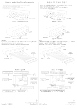
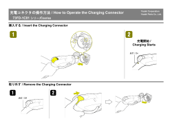
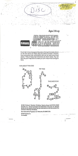

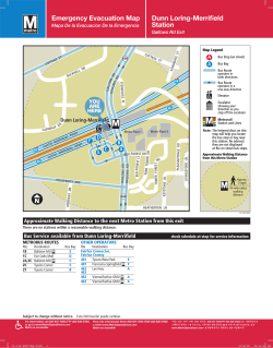
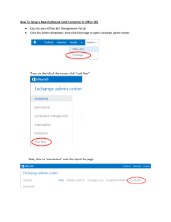

© Copyright 2026