
TECHNICAL MANUAL VERSION 9.2
TECHNICAL MANUAL VERSION 9.2
TECHNICAL MANUAL VERSION 9.2
CIRTECH ELECTRONICS (PTY) LTD
INDEX
Section
Contents
1.
2.
3.
4.
4.1
4.2
4.2.1
4.2.2
4.2.3
4.2.4
4.2.5
4.2.6
4.2.7
4.2.8
4.2.9
4.2.10
4.2.11
4.2.12
4.2.13
4.2.14
4.2.15
5.
5.1
5.2
5.2.1
5.2.2
5.2.3
5.2.4
5.2.5
5.2.6
5.2.7
5.2.8
5.2.9
5.2.10
5.2.11
5.2.12
5.2.13
5.2.14
5.2.15
5.2.16
How to Contact Us
Revision Control
Introduction
Local Manufacturing
Product Listing
Capabilities
Laminate Thickness
Copper Plating
Maximum Panel Sizes
Holes (Drilled)
Aspect Ratio
Annular Ring (Edge of Drill to Edge of Pad)
Track and Gap
Minimum Copper Clearance for PCB Profiling
Surface Finishes
Masks and Inks
Inspection and Testing
Reports
Preferred Software Formats
Warp and Twist Factor
Quality Standards and Systems
Offshore Manufacturing
Product Listing
Capabilities
Material Types
Laminate thickness tolerance
Conductor Widths and Spacing
Drilled Hole Diameters
Hole Positional Tolerances
Hole Size Tolerances
Requirements for resin hole plugging
Countersunk holes
Conductor Metal Finishes
Screen Printed Inks
Soldermask
Legend (Silkscreen)
Board Profiling
Slot Tolerances
Minimum Distance Between Holes / Slots
Warp and Twist
© Cirtech Electronics 2012. All Rights Reserved. www.cirtech-electronics.com
Page No.
4
5
6
8
8
8
8
8
9
9
9
9
9
9
10
10
10
10
10
10
10
11
11
11
12
12
12
13
13
13
14
14
14
15
16
16
16
17
17
17
PAGE 2 OF 72
TECHNICAL MANUAL VERSION 9.2
CIRTECH ELECTRONICS (PTY) LTD
INDEX CONTINUED…
Section
Contents
5.2.17
5.2.18
6.
7.
8.
9.
10.
Bare Board Electrical Testing
Quality Standards and Systems
Design Guidelines
RoHS Compliance
Glossary of Terms
Appendix
Personal Notes
© Cirtech Electronics 2012. All Rights Reserved. www.cirtech-electronics.com
Page No.
17
18
19
55
58
67
72
PAGE 3 OF 72
TECHNICAL MANUAL VERSION 9.2
CIRTECH ELECTRONICS (PTY) LTD
1. HOW TO CONTACT US
Cape Town Head Office
Cirtech House, Unit A
Stibitz Road
Westlake Business Park 2
Tokai 7945
Cape Town
South Africa
PO BOX 166
Constantia
7848
Cape Town
Telephone
Fax
+ 27 21 700 4900
+ 27 21 701 2322
Operations Director
Stephen Sher
[email protected]
021 700 4906
Financial Director:
Sascha Bierberg
[email protected]
021 700 4911
Customer Service:
Libby Van Zyl
[email protected]
021 700 4905
Quotes and Sales:
Marcel Henry
[email protected]
021 700 4918
Technical Engineer:
Kevin Emslie
[email protected]
021 700 4900
Leon Poulton
[email protected]
083 364 5728
Gauteng Sales
Sales & Marketing Manager:
© Cirtech Electronics 2012. All Rights Reserved. www.cirtech-electronics.com
PAGE 4 OF 72
TECHNICAL MANUAL VERSION 9.2
CIRTECH ELECTRONICS (PTY) LTD
2.REVISION CONTROL
Manual
Revision
Date of
Issue
Page No
Revision Details
1
2
3
4
4.1
4.2
4.3
4.4
5.0
5.1
6.0
6.0A
7.0
8.0
9.0
9.1
9.2
24-Jan-2000
27-Jul-2000
03-Aug-2000
31-Nov-2000
06-Nov-2000
04-April-2001
28-May-2001
14-March-2002
05-March-2003
28-Aug-2003
09-Feb-2005
28-June-2006
05-March-2007
14-March-2008
28-Jan-2009
03-Dec-2009
26-Jan-2012
All
All
All
All
All
All
All
All
All
1&2
1&2
2&3
All
All
All
All
All
First issue.
Added Material Construction Section 5.3
Added Section “How to Contact Us”.
Company Name changed.
Contact Details and Logo Modification.
All sections updated to latest specifications.
Contact Details, drawing added and new cover design.
Updated Gauteng Sales details.
Added Microvia Design Rules and Updated all specifications and drawings.
Updated Section “How to Contact Us”
Updated Section “How to Contact Us”
Updated Section “How to Contact Us”
Updated total manual to include RoHS and CircuitExpress
Updated total manual and CircuitExpress details
Updated total manual and CircuitExpress details
Removed CircuitExpress page
Updated total manual, included Cirtech local manufacturing
© Cirtech Electronics 2012. All Rights Reserved. www.cirtech-electronics.com
PAGE 5 OF 72
TECHNICAL MANUAL VERSION 9.2
CIRTECH ELECTRONICS (PTY) LTD
3.INTRODUCTION
Objective of this Manual
To present the full range of products and services offered by Cirtech Electronics to people involved in
the design and purchase of Printed Circuit Boards.
Detailed descriptions of the technology and its capabilities are presented along with the materials
and manufacturing tolerances applicable to the various materials and product types.
Design Guide
Containing production costs without sacrificing quality and standards is always a delicate balancing
act that begins at the design stage. Section 6: Design Guidelines, details design and material
utilization methods that will ensure more cost effective and reliable PCB production.
Total Quality Control
To ensure the delivery of a superior product, total Quality Control is essential. To this end, Cirtech
personnel undertake regular inspection visits to the facilities of our offshore suppliers. We audit their
processes and documentation control to ensure that quality is not being compromised. We only use
manufacturers with facilities that carry international standards certification.
Staying Abreast of Technology
With the constant advances in manufacturing and component technology, boards are getting
increasingly smaller and more densely populated. PCB designers are squeezing more and more
performance from their products. Manufacturers have to maintain quality and meet the challenges
that miniaturisation, higher component density and increased performance bring. The off-shore
manufacturing facilities we use are continually updating their plants and the skills of their personnel
to ensure that they keep pace with developments.
Cirtech Manufacturing – South African PCB Fabrication
Since the world-wide economic turmoil of 2007 / 2008, there has been an increasing demand for a
more secure and reliable source of quality electronic products and components. In response to this,
the Cirtech Group acted on a long held plan to open a PCB manufacturing plant in Cape Town.
Cirtech Manufacturing started production at the beginning of 2010.
The facility was commissioned from scratch and is equipped with the latest and most advanced PCB
fabricating equipment available. To ensure that the plant performed to its highest capabilities,
internationally recognized engineers were brought in to assist with the commissioning and running of
the plant.
In accordance with best practice, the entire manufacturing process is contained under one roof, in a
dust proof, air conditioned environment. Temperature-sensitive materials used in PCB manufacture
are stored in a dedicated cold-room. Everything from front-end engineering to the packaging of the
finished product is done on the premises.
To reduce human interaction with the manufacturing process as much as possible, our line is fully
© Cirtech Electronics 2012. All Rights Reserved. www.cirtech-electronics.com
PAGE 6 OF 72
TECHNICAL MANUAL VERSION 9.2
CIRTECH ELECTRONICS (PTY) LTD
3.INTRODUCTION CONTINUED…
automated.
The plant has an in-house chemistry laboratory which is dedicated to maintaining the bespoke
chemistry used in the various processes on the line. This facility ensures that the chemicals in the
plating tanks are kept to optimum levels and that specifications are rigidly adhered to.
Quality Control is an integral part of the manufacturing process. Automated Optical Inspection (AOI)
is carried out on the inner layers during manufacture; micro-sectioning and comprehensive electrical
testing is carried out on all orders. All product leaves the plant in hermetically sealed packaging to
guarantee protection against moisture and dust which would adversely affect solderability.
The plant is set up on a “per panel” policy. This enables us to schedule jobs as they come in,
regardless of their size or complexity. We don’t have to re-jig the line to accommodate each job.
This gives us the greatest possible flexibility and excellent turn-around time.
Peripheral Products
Apart from sourcing and manufacturing PCBs, Cirtech Electronics supplies comprehensive range of
high quality peripheral equipment and components such as stainless steel, laser-cut solder paste
stencils, semi-rigid and flexi-circuits and the entire range of Xiamen Zettler equipment which includes
the highest quality liquid crystal displays and a full range of transformers. Please contact us for
detailed information on the peripheral equipment we supply.
Customer Satisfaction through Communication
Cirtech staff members pride themselves on knowing what our clients’ needs are and how best to meet
them. Our well established network of component suppliers and PCB manufacturers coupled with our
own manufacturing capacity allows us to access the best possible solution for your requirements.
This Technical Manual is also available on our website, see
http://www.cirtech-electronics.com/downloads.html
© Cirtech Electronics 2012. All Rights Reserved. www.cirtech-electronics.com
PAGE 7 OF 72
TECHNICAL MANUAL VERSION 9.2
CIRTECH ELECTRONICS (PTY) LTD
4.LOCAL MANUFACTURING
4.1. PRODUCT LISTING
1.
2.
3.
4.
5.
Single Sided PCB
Double Sided Non-Plated Through Hole PCB
Double Sided Plated Through Hole PCB
Multilayer PCB Up To 4 Layers
Laser Cut Stencils (Sourced Offshore)
4.2. CAPABILITIES
This section describes in detail the currently available PCB manufacturing technology levels at our
local manufacturing facility.
4.2.1. Laminate Thickness
Single Sided PCB
1.0mm FR4 35/00
1.6mm FR4 35/00
1.6mm CEM1 35/00
Double Sided PCB
0.8mm
1.0mm
1.0mm
1.6mm
1.6mm
4 Layer Multilayer PCB
0.8mm FR4 18/18 Core Material
1.0mm FR4 35/35 Core Material
Outer Layer Copper Foils
18um
Pre-Pregs
1060
1080
2113
7628
=
=
=
=
FR4
FR4
FR4
FR4
FR4
2.1
2.5
3.8
7.0
18/18
18/18
35/35
18/18
35/35
mil
mil
mil
mil
=
=
=
=
0.053mm
0.063mm
0.100mm
0.180mm
4.2.2. Copper Plating
Finished Copper Thickness
Edge Plated Half Holes
38um and 55um
as Per Customer Specification
© Cirtech Electronics 2012. All Rights Reserved. www.cirtech-electronics.com
PAGE 8 OF 72
TECHNICAL MANUAL VERSION 9.2
CIRTECH ELECTRONICS (PTY) LTD
4.LOCAL MANUFACTURING CONTINUED…
4.2.3. Maximum Panel Sizes
Single and Double Sided
Multilayer
425mm x 500mm
245mm x 365mm
4.2.4. Holes (Drilled)
Minimum Hole Diameter
Hole Tolerances
Maximum Hole Diameter
0.3mm
PTH <1.5mm = ±0.05mm
PTH ≥1.5mm = ±0.1mm
NPTH <1.0mm = ±0.05mm
NPTH ≥1.0mm = ±0.1mm
5.0mm
4.2.5. Aspect Ratio
Maximum (1.6mm)
5.3 : 1 (Board Thickness / Hole Diameter)
4.2.6. Annular Ring (Edge of Drill to Edge of Pad)
Minimum for Vias
Minimum for Components
Minimum for Non Plated Hole
0.150mm
0.200mm
0.225mm
4.2.7. Track and Gap
Minimum Track and Gap 35um Copper Finish
Minimum Track and Gap 55um Copper Finish
Minimum Soldermask Line (Between IC Pads)
Minimum Solder Mask Pad Swell
Minimum Edge of Drill to Conductor
Inner Layer Copper Clearance
Drilled Hole Edge to copper on inner layers
0.15mm (6 mil)
0.254mm (10 mil)
0.1524mm (6 mil)
8 mil larger than copper pad
0.1524mm (6 mil)
0.25mm (10 mil)
0.25mm (10 mil)
4.2.8. Minimum Copper Clearance for PCB Profiling
Edge of board for NC Routing
NC Routing Tolerance
Edge of Board for V-Scoring
V-Scoring Tolerance
V-Scoring Web Thickness
V-Score Angle
0.35mm (14 mil)
± 0.2mm
0.5mm (20 mil)
± 0.20mm
0.4mm
30º
© Cirtech Electronics 2012. All Rights Reserved. www.cirtech-electronics.com
PAGE 9 OF 72
TECHNICAL MANUAL VERSION 9.2
CIRTECH ELECTRONICS (PTY) LTD
4.LOCAL MANUFACTURING CONTINUED…
Any combination of the above methods may be utilized to achieve the final board profile within the
required panel layout.
4.2.9. Surface Finishes
H.A.S.L
ENIG
(Tin / Lead)
(RoHS Compliant)
For more detail on the finishes refer to Appendix “B”.
4.2.10. Masks and Inks
Solder Mask
Ledgend
Peelable Mask
Green (Preferred). Also Blue, Black, White and Red on request. (PhotoImagable)
White (Preferred). Black on Request. (Photo-Imagable)
Peters SD2954 and Peters SD2955.
4.2.11. Inspection and Testing
Visual Inspection
Fly Probe
100% on all products
100% Tested (Available on Request)
4.2.12. Reports
Inspection Report
Micro Section
Available on Request
Available on Request
4.2.13. Preferred Software Formats
Gerber
Drill
PCB Spec / Instructions
RS274X
Excellon
PDF, Word or mechanical gerber layer.
4.2.14. Bow and Twist Factor
Single Sided PCB
Double Sided PCB
Multilayer PCB
1.0%
0.75%
0.75%
4.2.15. Quality Standards and Systems
IPC-A-600
ISO9002 / 2008
See Appendix “C” for a description of the above.
© Cirtech Electronics 2012. All Rights Reserved. www.cirtech-electronics.com
PAGE 10 OF 72
TECHNICAL MANUAL VERSION 9.2
CIRTECH ELECTRONICS (PTY) LTD
5. OFFSHORE MANUFACTURING
5.1. PRODUCT LISTING
1. Single Sided PCB
2. Double Sided Non-Plated Through Hole PCB
3. Double Sided Plated Through Hole PCB
4. Multilayer PCB From 4 To 40 Layers Count
5. Blind And Buried Via Technology Multilayers
6. Single Sided Flexible And Flexi Rigid Circuits
7. Double Sided Through Hole Plated Flexible And Flexi Rigid Circuits
8. Multilayer Flexible And Flexi Rigid Circuits
9. Special Materials (Rogers Corp, Aluminium Substrate, HDI Etc)
10. Membrane Switches, Plastic Enclosures, Moulded Plastic Parts, Silicone Rubber
11. Keypads, LCD Displays, Transformers And Coils
12. Laser Cut Stencils
5.2. CAPABILITIES
This section describes in detail the currently available PCB manufacturing technology levels at our
offshore facilities.
Rigid boards
Flexi-rigid boards
up to 40 layer multilayer
up to 20 layer multilayer
Rigid PCB thickness range
0.13mm to 7.0mm
Maximum PCB / panel size
584mm x 889mm
Minimum core thickness
0.05mm (2mil) without blind and buried vias
0.13mm (5mil) with blind and buried vias.
Impedance testing tolerance
±5Ω for requirements under 50 Ω
±10% for 50Ω and above
Tolerance for multi-layer registration is ≤ 0.127mm (5 mil).
© Cirtech Electronics 2012. All Rights Reserved. www.cirtech-electronics.com
PAGE 11 OF 72
TECHNICAL MANUAL VERSION 9.2
CIRTECH ELECTRONICS (PTY) LTD
5. OFFSHORE MANUFACTURING CONTINUED…
5.2.1. Material Types
CEM-1
CEM-3
FR4 Normal Tg
FR4 High Tg
FR4 Normal Tg Halogen Free
FR4 High Tg Halogen Free
Hydrocarbon Ceramic high freq
PTFE high frequency material
PTFE Bonding Film
Operating temp 130ºC, CTE 1.3, Water absorption 0.30
Operation temp 130ºC, CTE 1.2, Water absorption 0.25
S1141
FR408, IT180A, PCL-370HR, N4000-13, N4000-13SI
S1155
S1165
Rogers4350, Rogers4003, 25FR, 25N
Rogers Series, Taconic Series, Arlon Series, Nelco Series
RO3001 (1.5mil), HT1.5 (1.5mil), Cuclad6700 (1.5mil)
5.2.2. Laminate thickness tolerance
+/-0.1mm for boards less than or equal to 1.0mm thick.
+/-10% for boards greater than 1.0mm thick.
5.2.3. Conductor Widths and Spacing
Inner Layer
Copper weight
0.5oz Copper
1oz Copper
2oz Copper
3oz Copper
4oz Copper
5oz Copper
Minimum Width
0.076mm (3mil)
0.076mm (3mil)
0.127mm (5mil)
0.152mm (6mil)
0.178mm (7mil)
0.254mm (10mil)
Minimum Spacing
0.076mm (3mil)
0.102mm (4mil)
0.127mm (5mil)
0.178mm (7mil)
0.279mm (11mil)
0.406mm (16mil)
Outer Layer
Copper Weight
0.5oz Copper
1oz Copper
2oz Copper
3oz Copper
4oz Copper
5oz Copper
Conductor width tolerance
Minimum Width
0.089mm (3.5mil)
0.114mm (4.5mil)
0.152mm (6mil)
0.203mm (8mil)
0.254mm (10mil)
0.305mm (12mil)
Minimum Spacing
0.089mm (3.5mil)
0.127mm (5mil)
0.203mm (8mil)
0.356mm (14mil)
0.406mm (16mil)
0.508mm (20mil)
≤0.254mm (10mil): ±0.0254mm (1.0mil)
>0.254mm (10mil): ±0.0381mm (1.5mil)
© Cirtech Electronics 2012. All Rights Reserved. www.cirtech-electronics.com
PAGE 12 OF 72
TECHNICAL MANUAL VERSION 9.2
CIRTECH ELECTRONICS (PTY) LTD
5. OFFSHORE MANUFACTURING CONTINUED…
5.2.4. Drilled Hole Diameters
Mechanical Drilling (finished hole size)
Overall 0.10mm to 6.5mm (4mil to 256mil)
Minimum hole size for PTFE material
Maximum hole size for blind and buried vias
Maximum hole size for solder mask plugging
Minimum connecting hole size
0.25mm
0.30mm
0.30mm
0.35mm
(10mil)
(12mil)
(12mil)
(13.8mil)
Hole sizes when plugging with resin 0.10mm (4mil) to 0.4mm (16 mil)
Maximum PCB thickness for 0.10mm (4mil) mechanically drilled hole is 0.6mm (24mil)
Maximum PCB thickness for a 0.15mm (6mil) mechanically drilled hole is 1.2mm (47mil)
Laser Drilling (finished hole size)
Blind hole size if plugging with resin
Blind hole size if filling with plating
0.075mm (3mil) to 0.15mm (6mil)
0.075mm (3mil) to 0.127mm (5mil)
The aspect ratio is less than or equal to 16:1 (tool size greater than 0.2mm)
Laser drilling technology makes diameters of 0.1mm and smaller possible for blind and buried via
hole technology multilayers.. Minimum hole size is dependant on the thickness of the inner layer core
material.
5.2.5. Hole Positional Tolerances
Tolerances
Drilled hole to drilled hole (same set up)
± 0.08mm (3.15mil)
Drilled hole to second drilled hole ( different set up)
± 0.15mm (6mil)
Reference drilled hole to routed edge
± 0.13mm (5mil)
Reference drilled hole to V-Cut edge
± 0.13mm (5mil)
5.2.6. Hole Size Tolerances
PTH hole size tolerance
NPTH size tolerance
© Cirtech Electronics 2012. All Rights Reserved. www.cirtech-electronics.com
±0.076mm (±3mil)
±0.051mm (±2mil)
PAGE 13 OF 72
TECHNICAL MANUAL VERSION 9.2
CIRTECH ELECTRONICS (PTY) LTD
5. OFFSHORE MANUFACTURING CONTINUED…
5.2.7. Requirements for resin hole plugging (finished hole size and pcb thickness)
Finished Hole Size
0.10mm (4mil) and 0.15mm (6mil)
0.20mm (8mil)
0.25mm (9.8mil)
0.3mm (11.8mil)
PCB Thickness
≤1.6mm (63mil)
≤2.4mm (94mil)
≤2.8mm (110mil)
≤3.2mm (126mil)
5.2.8. Countersunk holes
Special drill bits 82º, 90º and 120º, hole sizes 0.3mm (12mil) to 10mm (393.7mil).
Standard drill bit 130º, hole sizes less than or equal to 3.175mm (125mil).
Standard drill bit 165º, hole sizes between 3.175mm (125mil) and 6.5mm (256mil).
Angle tolerance
Hole size tolerance
Depth tolerance
±10º
±0.20mm (7.8mil)
±0.15mm (6mil)
5.2.9. Conductor Metal Finishes
There are various types of surface finishes that can be applied to the PCB and the following table
briefly describes the types that Cirtech currently supplies.
Board Finish
Advantage
Organic Coating
(OSP)
Good co-planarity
Hot Air Solder
Level (HASL)
Tin / Lead
Hot Air Solder
Level (HASL)
Lead Free
Electroless
Nickel
Immersion Gold
(ENIG)
Full Gold
Good solderability
Good solderability
Remarks
Copper finish PCB coated with an
anti tarnish coating. Limited shelf
life.
Exposed copper areas are coated
with Tin –Lead after Soldermask
application.
Exposed copper areas are coated
with Tin –Lead after Soldermask
application.
RoHS Compliance
RoHS Compliant
Non RoHS
Complaint
Non RoHS
Complaint
Good co-planarity
Soft gold, coated only on pads free
from Soldermask. Cirtech’s
preferred RoHS finish
RoHS Compliant
Hard Gold for
Sliding Contact
Surfaces
Hard Gold plated prior to etching.
Other exposed copper areas are TinLead coated.
Non RoHS
Complaint
© Cirtech Electronics 2012. All Rights Reserved. www.cirtech-electronics.com
PAGE 14 OF 72
TECHNICAL MANUAL VERSION 9.2
CIRTECH ELECTRONICS (PTY) LTD
5. OFFSHORE MANUFACTURING CONTINUED…
5.2.9. Conductor Metal Finishes Continued…
Board Finish
Advantage
Remarks
RoHS Compliance
Immersion
Silver
Good co-planarity
Coated only on pads free from
Soldermask.
RoHS Compliant
Immersion Tin
Good co-planarity
Coated only on pads free from
Soldermask. Very limited shelf
life.
RoHS Compliant
OSP for BGA’s, ENIG. OSP has a
very limited shelf life.
RoHS Compliant
ENIG and OSP
Good co-planarity
Minimum gap between pads for ENIG is 0.10mm (4mil).
Minimum gap between gold fingers is 0.15mm (6mil).
Minimum gap between pads for HASL is 0.178mm (7mil).
For more detail on the finishes refer to appendix “B” on page 67.
5.2.10 Screen Printed Inks
5.2.10.1. Conductive Ink
Touch Contact Pads and Links.
Minimum gap between carbon pads
Thickness range
Carbon Print to Conductive Pattern tolerance
5.2.10.2. Peelable Blue Mask Ink
0.38mm (15mil)
0.10mm (4mil) to 0.35mm (14mil)
± 0.25mm (10mil)
To mask off areas not required to be wave soldered.
Short shelf life.
Minimum gap ( peelable solder mask and pad)
0.4mm (16mil)
Thickness range
0.2mm (8mil) to 0.5mm (20 mil)
Peelable mask to Conductive Pattern tolerance
± 0.40 (16mil)
© Cirtech Electronics 2012. All Rights Reserved. www.cirtech-electronics.com
PAGE 15 OF 72
TECHNICAL MANUAL VERSION 9.2
CIRTECH ELECTRONICS (PTY) LTD
5. OFFSHORE MANUFACTURING CONTINUED…
5.2.11. Soldermask
Liquid Photo-imagible Solder Mask
Curtain Coat and Flood Screen application methods.
Available in Green (preferred), yellow, black, blue, red,
white and matt green.
Minimum gap ( solder mask and pad)
0.15mm (6mil)
Thickness range
10um to 18 um on copper area
5um to 8 um on via pad and line corner
Solder mask to Conductive Pattern tolerance
± 0.13 (5mil)
Minimum bridge width (green)
0.10mm (4mil)
Minimum bridge width (other colors)
0.127mm (5mil)
5.2.12. Legend (Silkscreen)
Available in White, yellow and black.
Serial number, bar code and planar code can be printed if using the white legend.
Minimum text width (0.5oz based Copper)
0.1mm (4mil)
Minimum text height (0.5oz Copper)
0.6mm (23mil)
Legend to Conductive Pattern tolerance
0.15mm (6mil)
5.2.13. Board Profiling
Punching
Hardened tool for cost effective profiling of volume PCB’s.
Punch & Pushback
Board punched and returned to the panel for easy
removal after assembly. Tool required.
NC-Routing
Tab Break-away methods.
Minimum distance between PCB edge and nearest copper feature
is .2mm (8mil).
Slot size tolerance is 0.15mm (6mil)
V-Scoring
Remaining web thickness 0.4mm.
Angle tolerance is +/- 5º
Symmetrical tolerance is +/-0.10mm (4mil)
Web thickness tolerance is +/-0.10mm (4mil)
© Cirtech Electronics 2012. All Rights Reserved. www.cirtech-electronics.com
PAGE 16 OF 72
TECHNICAL MANUAL VERSION 9.2
CIRTECH ELECTRONICS (PTY) LTD
5. OFFSHORE MANUFACTURING CONTINUED…
Any combination of the above methods may be utilized to achieve the final board profile within the
required panel layout.
V-Scoring - Distance required between PCB edge and nearest copper feature
V-Scoring
tool angle
20º
30º
45º
60º
Less than or
equal to 1.0mm
0.30mm (12mil)
0.33mm (4mil)
0.37mm (15mil)
0.42mm (17mil)
Above 1mm and up
to 1.6mm
0.36mm (14mil)
0.40mm (16mil)
0.50mm (20mil)
0.60mm (24mil)
Above 1.6mm and up
to 2.4mm
0.42mm (17mil)
0.51mm (20mil)
0.64mm (25mil)
0.80mm (31mil)
Between 2.5mm and
3.0mm
0.47mm (19mil)
0.59mm (23mil)
0.77mm (30mil)
0.97mm (38mil)
PCB outline dimension and location tolerance is +/-0.1mm.
5.2.14. Slot Tolerances
Slot Width Tolerance
Slot Length Tolerance
± 0.15mm (6mil)
± 0.15 (6mil)
5.2.15. Minimum Distance Between Holes / Slots
Min distance hole wall to hole wall 0.2mm (8mil)
5.2.16. Warp and Twist Factor
PCB
–
0.1%
Warp and Twist Flatness
PCB Thickness
Percentage
mm
inches
0.8 ~ 1.60
0.032 ~ 0.063
0.75
5.2.17 Bare Board Electrical Testing
Fine lead pitch SMD devices with 0.254mm (10mil) pitch between leads.
Net List testing to Gerber data utilising dedicated Test Fixtures.
Dual access fixtures for simultaneous testing of Double Sided SMD boards.
© Cirtech Electronics 2012. All Rights Reserved. www.cirtech-electronics.com
PAGE 17 OF 72
TECHNICAL MANUAL VERSION 9.2
CIRTECH ELECTRONICS (PTY) LTD
5. OFFSHORE MANUFACTURING CONTINUED…
Maximum test voltage
Maximum test current
–
–
500V
200mA
The test fixture is a dedicated hardware tool that is built up specifically for the particular PCB and the
spring loaded test pins are permanently fastened to the fixture plates ensuring long term reliability
and repeatability.
The cost of these dedicated pins is a major contributor to the overall cost of the test fixture.Design of
the test pin requirements is generated from the original gerber data as supplied by the customer
through the use of software that creates the net-list that results in the drill file for creating the test
fixture plates. The net-list is consequently used to program the test equipment computer to that
specific board layout.
If the board design has Surface Mount Components on both sides, a double sided fixture is created
that allows simultaneous testing of both sides to ensure complete testing on nets that originate on one
side and terminate on the other side through via holes.
Testing with a dedicated net-list driven test fixture is one of the best methods as this will ensure that
testing is 100%.
5.2.18. Quality Standards and Systems
UL94
IPC-A-600
QS9000
ISO9002:2000
ISO14001
TS16949
See Appendix “C” for a description of the above.
© Cirtech Electronics 2012. All Rights Reserved. www.cirtech-electronics.com
PAGE 18 OF 72
TECHNICAL MANUAL VERSION 9.2
CIRTECH ELECTRONICS (PTY) LTD
6. DESIGN GUIDELINES
Manufacturing of Printed Circuit Boards, whether they be Single Sided, Double Sided or Multilayer,
requires a certain sequence of operations that vary depending upon the type and complexity of the
design. The number of major operations ranges from 8 for a simple Single Sided board to in excess of
25 for complex Multilayer boards. Each of these manufacturing stages has optimum parameters and
associated tolerances that have a direct influence on the cost of the finished product. By designing
within these parameters it is possible to substantially reduce the cost of a PCB design. To achieve the
goal of cost reduction, the designer should have an in depth understanding of the processes. It is the
objective of this section to provide the designer of Printed Circuit Boards with all the information
required to generate cost effective PCB layouts.
This section also includes design tips and information that will enhance the final quality of the PCB
being designed.
Section Contents:
DATA PACKAGE FOR COSTING PURPOSES (6.1)
This sub-section details the type of information that must be included in the submitted data package
so that accurate quotations can be generated.
PRINTED CIRCUIT BOARD MANUFACTURING PROCESS FLOW (6.2)
Flow diagrams and descriptions of the various processes required to manufacture the three different
classes of PCB, which are Single Sided, Double Sided and Multilayer.
DESIGNING TO PROCESS PARAMETERS (6.3)
The criteria for each process are evaluated with respect to cost reduction and quality issues where
applicable. Through the use of drawings, tables and text, the optimum design parameters will be
revealed.
DESIGN RULES FOR MICROVIA (BLIND AND BURIED VIA) (6.4)
With the use of Laser-via process, blind micro-via can be obtained, resulting in much desired PCB
miniaturization. Available laser-via sizes range from 75µm to 250µm. Less space is required on the
PCB for laser drilling than for mechanical drilling.
© Cirtech Electronics 2012. All Rights Reserved. www.cirtech-electronics.com
PAGE 19 OF 72
TECHNICAL MANUAL VERSION 9.2
CIRTECH ELECTRONICS (PTY) LTD
6. DESIGN GUIDELINES CONTINUED…
6.1. DATA PACKAGE FOR COSTING PURPOSES
To ensure accurate costing of the PCB design, the following information must be included in the
package:
6.1.1. GERBER DATA
Gerber data files may be supplied in either of the following two formats:
RS-274-D
RS-274-X
Non-embedded aperture data format.
Embedded aperture data format (Preferred).
Example RS-274-D
Example RS-274-X
G04 Layer 7
G54D71*
G54D233*
X9910Y10731D03*
X9932Y10865D03*
X10207Y10830D03*
X10042Y11145D03*
X9852Y11235D03*
X9832Y11490D03*
X9847Y11645D03*
X9912Y11935D03*
X10002Y11885D03*
Y11985D03*
X9917Y12035D03*
X9927Y12135D03*
X9932Y12215D03*
Y12335D03*
X10002Y12400D03*
Y12255D03*
X9997Y12085D03*
X10297D03*
X10272Y12240D03*
G04 Layer 4
%FSLAX53Y53*%
%MOIN*%
%SFA1.000B1.000*%
%MIA0B0*%
%IPPOS*%
%ADD15C,0.04000*%
%ADD22USER22*%
%ADD26C,0.05900*%
%ADD27C,0.06000*%
%ADD72R,0.11800X0.04000*%
%ADD35USER35*%
%ADD39O,0.06000X0.08000*%
%LN1620c042.spl*%
%SRX1Y1I0J0*%
G54D15*
%LPD*%
G54D63*
X3419Y5919D03*
Y6116D03*
G54D22*
X3345Y6633D03*
© Cirtech Electronics 2012. All Rights Reserved. www.cirtech-electronics.com
PAGE 20 OF 72
TECHNICAL MANUAL VERSION 9.2
CIRTECH ELECTRONICS (PTY) LTD
6. DESIGN GUIDELINES CONTINUED…
Gerber files for the following layer types must be included, depending on the PCB type:
(S/S = Single Sided D/S = Double Sided MLB = Multilayer)
Component Side Peelable Mask
Component Side Silkscreen Legend
Component Side Soldermask
Component Side Conductive Carbon
Component Side Solderpaste Stencil
Component Side Copper Circuit Layer
Inner Ground Plane Layer
Inner Power Plane Layer
Inner Signal Layers
Solder Side Copper Circuit Layer
Solder Side Solderpaste Stencil
Solder Side Conductive Carbon
Solder Side Soldermask
Solder Side Silkscreen Legend
Solder Side Peelable Mask
Mechanical Drawing
(D/S, MLB)
(S/S, D/S, MLB)
(S/S, D/S, MLB)
(D/S, MLB)
(D/S, MLB)
(D/S, MLB)
(MLB only)
(MLB only)
(MLB only)
(S/S, D/S, MLB)
(S/S, D/S, MLB)
(S/S, D/S, MLB)
(S/S, D/S, MLB)
(D/S, MLB)
(S/S, D/S, MLB)
(S/S, D/S, MLB)
6.1.2. APERTURE LIST
Aperture lists are only required if the Gerber data is supplied in the RS-274-D format. The table below
describes the minimum required data to be included in the aperture listing.
D-CODE
SHAPE
X Mils
Y Mils
D10
Round
20.00
D11
Square
60.00
60.00
D12
Rectangle
16.00
80.00
D13
Round Rectangle
40.00
100.00
D14
Oblong
70.00
30.00
D15
Octagon
120.00
120.00
D16
Thermal
68.00
56.00
D17
Annulus
90.00
75.00
D18
Target
150.00
10.00
© Cirtech Electronics 2012. All Rights Reserved. www.cirtech-electronics.com
PAGE 21 OF 72
TECHNICAL MANUAL VERSION 9.2
CIRTECH ELECTRONICS (PTY) LTD
6. DESIGN GUIDELINES CONTINUED…
6.1.3. LAYER LISTING
To assist the PCB manufacturer to easily identify which gerber files are used for the
individual layers, it is recommended that a text file is included in the package. This text file must
describe the function of each gerber file. The table below is an example of this requirement.
GERBER FILE NAME
LAYER DESCRIPTION
1820D002.GBR
Component Side Silkscreen
1820D022.GBR
Component Side Soldermask
1820D032.GBR
Component Side Copper Circuit Layer
1820D042.GBR
Solder Side Copper Circuit Layer
1820D052.GBR
Solder Side Soldermask
1820D062.GBR
Mechanical Drawing
1820D072.DRL
Excellon Drill File
Metric Leading Format 4.3
6.1.4. DRILLING DATA FILE
The most commonly used format for Drill Files is the Excellon Format, which is supported on output
by most CAD software packages. Below is an abbreviated example of such a file.
M48
T1C28F0S0
T2C36F0S0
T3C40F0S0
%
T01
X379Y1213
X1474Y2493
X1294Y2838
T02
X1734Y1293
X999Y2783
T03
X294Y1493
X315Y2831
M30
© Cirtech Electronics 2012. All Rights Reserved. www.cirtech-electronics.com
PAGE 22 OF 72
TECHNICAL MANUAL VERSION 9.2
CIRTECH ELECTRONICS (PTY) LTD
6. DESIGN GUIDELINES CONTINUED…
6.1.5. MECHANICAL DRAWING
The mechanical drawing should be generated on any of the standard paper sizes such as A4, A3 and
A2 with the following information included on the drawing:
Revision Level of the Drawing/PCB
Part Number or Description of PCB
Material Type
–
Base Material, Copper Thickness and Laminate Thickness
Soldermask Ink type and Colour
Component Ink type and Colour
Carbon Conductive Ink requirements
Peelable Mask Ink requirements
Metal Finishes
–
Flux, OSP, Hot Air Level, Immersion Nickel Gold,
Gold Edge Connectors or other types of finish.
Tolerance of Board Profile Dimensions
Tolerance of Hole Size Diameters
Layer Build-up Sequence for Multilayers
Reference to in-house or International Specifications
Special Instructions
Drawing of the PCB Mechanical Profile Dimensions with Hole Position Symbol designations
Drawing of the PCB Panel Layout Dimensions (Fiducials and Tooling Holes)
See Appendix “A” for an example of a typical drawing that includes all of the above requirements.
© Cirtech Electronics 2012. All Rights Reserved. www.cirtech-electronics.com
PAGE 23 OF 72
TECHNICAL MANUAL VERSION 9.2
CIRTECH ELECTRONICS (PTY) LTD
6. DESIGN GUIDELINES CONTINUED…
PRINTED CIRCUIT BOARD MANUFACTURING PROCESS FLOW
6.2.1. SINGLE SIDED PROCESS FLOW
Copper Clad Laminate Preparation
Copper Pattern Image Resist Printing
Copper Etching
Resist Image Stripping
Soldermask Image Printing
Hot Air Leveling or Fluxing
Holes Punched or Drilled
© Cirtech Electronics 2012. All Rights Reserved. www.cirtech-electronics.com
PAGE 24 OF 72
TECHNICAL MANUAL VERSION 9.2
CIRTECH ELECTRONICS (PTY) LTD
6. DESIGN GUIDELINES CONTINUED…
6.2.2. DOUBLE SIDED AND MULTILAYER PROCESS FLOW
OUTE R LAYER PROCESS
Copper Clad Laminate Preparation
CNC Drilling
Electroless Copper Plating
INNE R LAYER PROCE SS
Copper Clad Innerco re
Preparation
Photo Imaging
Etching of Copper
Resist Stripping
Photo Imaging
Black Oxide
Copper Plating
Tin-Lead Plating
Layup (4 layer M ultilayer)
Resist Stripping
Vacuum Lamination
Etching of Copper
Tin-Lead Stripping
Soldermask Prin tin g
Hot Air Lev eling
© Cirtech Electronics 2012. All Rights Reserved. www.cirtech-electronics.com
PAGE 25 OF 72
TECHNICAL MANUAL VERSION 9.2
CIRTECH ELECTRONICS (PTY) LTD
6. DESIGN GUIDELINES CONTINUED…
6.3. DESIGNING TO PROCESS PARAMETERS
The following five subsections deal with the specific processes that are directly influenced by the
layout of the design and ultimately affect the price and quality of the final product.
6.3.1. MATERIAL UTILISATION
As the base material constitutes some 30% to 40% of the cost in PCB manufacturing, optimum
material utilisation plays an important role in a cost effective design through careful selection of
board and panel layout dimensions. Good material utilisation will result in 80% of the standard
manufacturing panel being used for actual board production.
For the purpose of optimising handling, material utilisation, transportation and inventory, the
following panel sizes are available:
Panel Sizes
Usable Panel Area
mm
inches
mm
inches
457 x 610
18 x 24
427 x 580
16.81 x 22.83
530 x 610
21 x 24
500 x 580
19.68 x 22.83
610 x 610
24 x 24
580 x 580
22.83 x 22.83
(Preferred Panel Size)
As can be seen from the above table of panel dimensions, the usable panel area is less than that of
the actual panel size. This is due to the manufacturer requiring a minimum border of 15mm all
around the panel for process tooling holes, identification data and clamping during plating processes.
To obtain optimum material usage from the manufacturing panel, the customer panel or individual
board size needs to be calculated back from the usable area dimensions as per the above table of
dimensions.
The three different methods of profiling panels and individual boards will have an influence on the
utilisation factor due to the different spacing requirements needed to achieve the profiles.
© Cirtech Electronics 2012. All Rights Reserved. www.cirtech-electronics.com
PAGE 26 OF 72
TECHNICAL MANUAL VERSION 9.2
CIRTECH ELECTRONICS (PTY) LTD
6. DESIGN GUIDELINES CONTINUED…
The following table and drawing indicate the spacing required for the panel profiling methods:
Profiling Method
Space Between Boards or Panels
Drawing Designation
V-Scoring
0.0mm
S
NC Routing
3.0mm
S
Punching 1.0mm
5.0mm
S
Punching 1.6mm
8.0mm
S
PANEL WIDTH
S
PCB 3
PCB 4
PCB 1
PANEL LENGTH
S
PCB 2
© Cirtech Electronics 2012. All Rights Reserved. www.cirtech-electronics.com
PAGE 27 OF 72
TECHNICAL MANUAL VERSION 9.2
CIRTECH ELECTRONICS (PTY) LTD
6. DESIGN GUIDELINES CONTINUED…
The carrier strips that are used on the customer panels for the purpose of assembly processes have a
negative influence on material utilisation. The drawing as below shows the four alternative methods of
using carrier strips, where applicable to the assembly process.
FOUR CARRIER STRIPS
TWO CARRIER STRIPS
ONE CARRIER STRIP
NO CARRIER STRIPS
Space wasted between the individual boards on the panel. The following drawing clearly indicates the
above criteria:
PANEL 1 V-Scored
PANEL 2 NC-Routed
Real Board Usage Area
Wasted Panel Area
Carrier Strip Area
3.0mm Router Path Area
© Cirtech Electronics 2012. All Rights Reserved. www.cirtech-electronics.com
PAGE 28 OF 72
TECHNICAL MANUAL VERSION 9.2
CIRTECH ELECTRONICS (PTY) LTD
6. DESIGN GUIDELINES CONTINUED…
The following drawing is an example of maximum material utilisation of the preferred panel size of
457mm x 610mm with an 88% utilisation factor.
457
213.0
213.0
15.0
15.0
15.0
PANEL 5
PANEL 6
193.0
PANEL 4
PANEL 3
193.0
PANEL 1
PANEL 2
193.0
© Cirtech Electronics 2012. All Rights Reserved. www.cirtech-electronics.com
610
15.0
PAGE 29 OF 72
TECHNICAL MANUAL VERSION 9.2
CIRTECH ELECTRONICS (PTY) LTD
6. DESIGN GUIDELINES CONTINUED…
SUMMARY:
1.
2.
3.
4.
Choose panel sizes that will best fit the usable area of the manufacturer’s panel.
Keep the carrier strip area of the panel to the minimum required.
Where possible, design rectangular boards for maximum material utilisation.
For irregular profile shapes, use rotations to best-fit shapes utilising combinations of NC
Routing and V-Scoring to achieve finished board/panel profiles.
© Cirtech Electronics 2012. All Rights Reserved. www.cirtech-electronics.com
PAGE 30 OF 72
TECHNICAL MANUAL VERSION 9.2
CIRTECH ELECTRONICS (PTY) LTD
6. DESIGN GUIDELINES CONTINUED…
6.3.2 DRILLING PARAMETERS
Drilling is one of the more expensive processes in PCB manufacturing and should therefore be given
detailed attention during the design stage. As the density of PCB design increases, the size of holes
and the relative pad sizes decrease correspondingly. Smaller drills tend to break more easily and
have a greater deflection during drilling. Consequently the drilling of small holes requires greater
precision machining. To maintain accuracy, the number of panels per stack for each drill spindle
and the in-feed rate has to be reduced. All these factors increase the cost for drilling of small Holes.
NOTE: COUNTER SUNK HOLES ARE NOT AVAILABLE AS A PROCESS
Due to the high cost factor of drilling, it is essential to note the following points during the design
stage.
6.3.2.1 SMALL DIAMETER HOLE DRILLING:
The table below indicates the relationship between drill diameters and stack heights of the base
laminate during the drilling process.
Drill Diameter
Material Stack Height 1.6mm Thick
Double Sided PCB
Multilayer PCB
< 0.40mm
2 up
2 up
0.40mm to 0.65mm
3 up
2 up
> 0.65mm
4 up
3 up
When selecting the finished hole sizes for components and via holes, the following data must be taken
into account as the actual drill size will be larger than the specified finished hole size. The reason for
this being that allowance for the copper, tin-lead or gold plating thickness must be made as specified
in the table below.
Metal Finish Type
Plating Thickness Allowance
Hot Air Leveled
Add 0.15mm (0.0006”)
Gold Finish
Add 0.10mm (0.004”)
Organic Surface Preparation
Add 0.10mm (0.004”)
© Cirtech Electronics 2012. All Rights Reserved. www.cirtech-electronics.com
PAGE 31 OF 72
TECHNICAL MANUAL VERSION 9.2
CIRTECH ELECTRONICS (PTY) LTD
6. DESIGN GUIDELINES CONTINUED…
From the above two tables it can be seen that selecting a 0.55mm finished via hole size in
conjunction with Hot Air Level finish, will result in a stack of 4 up with 1.6mm thick material.
The following drawing shows the difference between stack heights when using small diameter drill
bits.
Double Sided PcB
Finished Hole Size 0.55mm
Metal Finish: Hot Air Level
Drill Diameter:
(0.55 + 0.15) = 0.7mm
Stack Height = 4 up
Multilayer PcB
Finished Hole Size 0.40mm
Metal Finish: Gold Plated
Drill Diameter:
(0.40 + 0.10) = 0.5mm
Stack Height = 2 up
Drill Bit 0.7mm
Drill Bit 0.5mm
Entry Material
4 Sheets of
1.6mm
Material
2 Sheets of
1.6mm
Material
Back-up Material
6.3.2.2 GROUPING OF HOLE DIAMETERS
During the drilling cycle, all holes of the same diameter are drilled before the drill bit is changed for
the next diameter size. Re-tooling the drilling machine and in some cases re-stacking the boards,
takes time and lengthens the drilling cycle, thereby adding to cost. Where ever possible, keep the
number of different hole diameters to a minimum.
The following is an example of total drill bit reduction:
Drill List Strictly to Design Rules
0.7mm 0.8mm 0.9mm
1.2mm 1.3mm 1.4mm
Drill List Optimised
0.8mm
1.3mm
1.8mm 1.9mm 2.0mm
1.9mm
Through optimising the above example, the total number of drill sizes has been reduced from 9 bits
down to 3 bit sizes, thereby reducing the time cycle of drilling and consequently the cost.
© Cirtech Electronics 2012. All Rights Reserved. www.cirtech-electronics.com
PAGE 32 OF 72
TECHNICAL MANUAL VERSION 9.2
CIRTECH ELECTRONICS (PTY) LTD
6. DESIGN GUIDELINES CONTINUED…
6.3.2.3 NON PLATED THROUGH HOLES
An additional drilling cycle will be required if Non Plated Through Holes are drilled through copper
areas such as pads or ground planes. This additional drilling cycle will lead to higher cost of the
finished product. To avoid the additional drilling cycle, the NTHP and the THP holes must be drilled
in the same cycle. During the Photo-printing process the NTHP holes will be tented by the Photoresist
film only if there is no copper area around the NTHP holes. The tenting action will prevent the copper
plating solution from entering the barrel of the hole thereby retaining the hole as Non Plated.
The following drawings show in detail the methods required to achieve the above:
Non Plated Through Hole
with Copper Pads Requires
second drilling cycle.
Non Plated Through Hole
with no Copper Pad allows
Tenting of the hole by
Photoresist Film to prevent
plating of the hole.
Fibre Glass
Photoresist Film
Copper Pad
For Non Plated Through Hole
in Copper Ground Plane the
copper must be relieved by
=>1.0mm around the
circumference of the hole.
When routing tracks adjacent to
Non Plated Through Holes, there
must be =>1.0mm space between
the edge of the track and the hole
circumference.
1.0mm wide ring of Fibre Glass
Copper Ground Plane
=>1.0mm
NTHP Hole
© Cirtech Electronics 2012. All Rights Reserved. www.cirtech-electronics.com
PAGE 33 OF 72
TECHNICAL MANUAL VERSION 9.2
CIRTECH ELECTRONICS (PTY) LTD
6. DESIGN GUIDELINES CONTINUED…
6.3.2.4 SLOT DRILLING
Slots are produced either by drilling or routing. The choice depends on the size and finishing of these
slots. Drilling of slots is achieved by drilling a series of holes overlapping each other, until the full
length of the slot is reached. Inherent in such a process, are drill deflection issues that lead to slots
that are not straight (bean shaped), slot length reduced, broken drills and loss in positional accuracy.
To reduce such defects, the following details must be observed when designing slots:
DRILLED SLOT
SLOT WIDTH >= 1.0mm Diameter
W
SLOT LENGTH >= 2 times of the Slot Width
Length
6.3.2.5 ASPECT RATIO
The aspect ratio is defined as the panel thickness divided by the drilled hole diameter. This ratio
defines the limits for the capability of plating the barrel of the hole. The higher the aspect ratio
number, the greater the difficulty in achieving complete barrel plating.
Preferred Aspect Ratio Number:
Maximum Aspect Ratio Number:
6
8
The drawing below graphically displays examples of calculating the aspect ratio.
ASPECT RATIO 1
ASPECT RATIO 2
1.6mm / 0.3mm = 5.3
3.2mm / 0.4mm = 8
0.4mm
0.3mm
1.6mm
© Cirtech Electronics 2012. All Rights Reserved. www.cirtech-electronics.com
3.2mm
PAGE 34 OF 72
TECHNICAL MANUAL VERSION 9.2
CIRTECH ELECTRONICS (PTY) LTD
6. DESIGN GUIDELINES CONTINUED…
6.3.3
PHOTO-IMAGING OF COPPER CIRCUIT PATTERN
This section handles the aspects of copper circuit pattern layout with regards to all Plating and
Mechanical processes that follow on after the Photo-imaging process.
6.3.3.1 DENSITY DISTRIBUTION OF CIRCUITRY PATTERN
After imaging, the hole barrels and the circuitry pattern are plated to effect the necessary
interconnection between layers and the fulfillment of the current-carrying capacity that the PCB has
been designed for.
Copper is first plated, followed by a coating of tin-lead as an etch resist. This is an electrolytic plating
process, with the Electroless Copper (plated prior to photo-imaging), as the conductive base. By
means of electric current, Copper is plated onto the areas that are exposed from photo-resist. As only
one current can be applied to the panels, isolated traces and pads tend to accumulate more plating
whilst the high density copper areas will have a thinner distribution of Copper plating.
Uneven plating across the board will impair etching capabilities, resulting in over or under etching of
the PCB. This in turn, will translate into costly defects such as shorts, opens or reduced track widths
and spacing. Uneven plating will also lead to over and under sized hole diameters.
Circuit Density must be balanced across the entire surface of the PCB and this also applies to the
panel layout.
To achieve a balanced circuit density, the following points must be taken into account at the design
stage:
1.
2.
3.
Spread circuit density evenly across the whole surface of the PCB
Avoid isolated pads
Add plating robbers on “free” or less dense areas
By following the three points above, the following advantages will be achieved:
1.
2.
3.
Reduction of over-plating in less dense areas
Reduction of warp/twist incidence
Elimination of funneled through plated holes
© Cirtech Electronics 2012. All Rights Reserved. www.cirtech-electronics.com
PAGE 35 OF 72
TECHNICAL MANUAL VERSION 9.2
CIRTECH ELECTRONICS (PTY) LTD
6. DESIGN GUIDELINES CONTINUED…
The following drawing will graphically display the criteria for Balanced Circuit Layout.
PcB DESIGN WITH UNEVEN CIRCUIT DISTRIBUTION
HIGH DENSITY COPPER AREA
EXAMPLE PCB
LOW DENSITY COPPER AREA
EXAMPLE PCB
PcB DESIGN WITH ADDITIONAL COPPER ADDED TO BALANCE AREA
COPPER AS PER ORIGINAL UNBALANCED DISTRIBUTION OF AREA
ADDITIONAL COPPER ADDED TO BALANCE OUT THE COPPER AREA
© Cirtech Electronics 2012. All Rights Reserved. www.cirtech-electronics.com
PAGE 36 OF 72
TECHNICAL MANUAL VERSION 9.2
CIRTECH ELECTRONICS (PTY) LTD
6. DESIGN GUIDELINES CONTINUED…
6.3.3.2 CROSS- HATCHING OF GROUND PLANE COPPER AREA
Large Ground Plane areas should be crosshatched instead of creating solid areas of copper. There
are two advantages to using cross-hatching:
1.
2.
Reduction of high density plating areas that assists in balancing out copper density.
Improved adhesion of the Soldermask ink.
The following parameters should be applied when designing the crosshatched areas:
1.
2.
Minimum Line width
Minimum Space between Lines
0.4mm (0.016inch)
0.4mm (0.016inch)
The reason for preferring a minimum space of 0.4mm is to prevent the small squares of 0.4mm
Photo-resist Film from flaking of the base copper and creating open and short circuits.
The above points are detailed in the following drawing:
Detail
>=0.4mm
SOLID GROUND PLANE
CROSS HATCHED PLANE
LOW SOLDERMASK
ADHESION
GOOD SOLDERMASK ADHESION
POOR DENSITY DISTRIBUTION
IMPROVED DENSITY DISTRIBUTION
>=0.4mm
6.3.3.3 COPPER RELIEF FROM PROFILE EDGES
During the design stages, copper conductors must be kept clear of all profile edges. This will ensure
that during the profiling process, no copper will be exposed or burred. Ground planes on inner layers
of Multilayer boards must have copper relieved from the profile edges as per the drawings below. The
following profiling methods and profile shapes need to be considered as certain types require more
clearance than others.
© Cirtech Electronics 2012. All Rights Reserved. www.cirtech-electronics.com
PAGE 37 OF 72
TECHNICAL MANUAL VERSION 9.2
CIRTECH ELECTRONICS (PTY) LTD
6. DESIGN GUIDELINES CONTINUED…
1.
2.
3.
NC Routing
Punching
V-Scoring
–
–
–
Board Profile, Slots, Internal Cutouts
Board Profile, Slots, Internal Cutouts
Board Profile
The drawings below describe the clearance widths required for each of the three profiling methods.
NC Routing
NC ROUTING
NC ROUTING
Board Profile Clearance
NC ROUTING
Slot Profile Clearance
Internal Cutout Clearance
INTERNAL
>=0.3mm
CUTOUT
CLEARANCE
>=0.3mm
CLEARANCE
>=0.3mm
CLEARANCE
Board Edge
Ground / Trace
Ground / Trace
Ground / Trace
Slot Edge
Punching
PUNCHING
PUNCHING
Board Profile Clearance
PUNCHING
Slot Profile Clearance
Internal Cutout Clearance
INTERNAL
CUTOUT
>=0.5mm
CLEARANCE
>=0.5mm
CLEARANCE
>=0.5mm
CLEARANCE
Board Edge
Ground / Trace
Ground / Trace
Ground / Trace
Slot Edge
V-Scoring
V-SCORING
Board Profile Clearance
>=0.5mm
CLEARANCE
Copper Ground / Trace
Board Edge
V-Cut
© Cirtech Electronics 2012. All Rights Reserved. www.cirtech-electronics.com
PAGE 38 OF 72
TECHNICAL MANUAL VERSION 9.2
CIRTECH ELECTRONICS (PTY) LTD
6. DESIGN GUIDELINES CONTINUED…
6.3.3.4 THERMAL PADS ON GROUND PLANES
Thermal pads should be utilised when placing leaded component holes into ground plane areas. The
thermal pads will assist the soldering process by reducing the heat-sink effect created by the large
copper ground plane area. Without thermal pads, dry solder joints will result due to the soldering
heat being drawn away by the large copper plane area. These pads must be placed on outer layers
and inner layers of Multilayers that have ground plane layers. This will also apply to Double Sided
boards with ground plane areas.
Drawings below display examples of thermal pad shapes and clearance dimensions from the edge of
the hole to the inner ring of the thermal pad.
Thermal Pad Shapes
ROUND THERMAL
WITH FOUR SPOKES
AT 90 DEG ANGLE
ROUND THERMAL
WITH TWO SPOKES
AT 90 DEG ANGLE
>= 0.4mm
>= 0.4mm
SQUARE THERMAL
WITH FOUR SPOKES
AT 45 DEG ANGLE
>= 0.4mm
>= 0.3mm
>= 0.3mm
SQUARE THERMAL
WITH FOUR SPOKES
AT 90 DEG ANGLE
>= 0.3mm
CLEARANCE PAD
= Copper Ground Plane Area
>= 0.4mm
>= 0.5mm
>= 0.3mm
Care should be taken when placing thermal pads adjacent to clearance pads as a poor combination of
clearance pads around the thermal pad could effectively remove the spoke connections to the ground
plane causing the thermal pad to become isolated from the copper plane.
© Cirtech Electronics 2012. All Rights Reserved. www.cirtech-electronics.com
PAGE 39 OF 72
TECHNICAL MANUAL VERSION 9.2
CIRTECH ELECTRONICS (PTY) LTD
6. DESIGN GUIDELINES CONTINUED…
6.3.3.5 PHOTO-RESIST SLIVERS
Slivers are defined as very fine pieces of Photo-resist film that flake off the base copper during the
copper plating process. These slivers of film will then re-deposit on to the board surface and possibly
result in open or short circuits. If the film sliver deposits across a track, the tin-lead will not plate in
this area; during etching an open circuit will be created.
The following drawing graphically displays the two most common causes of slivers.
Tapers to below
0.10mm thickness
< 0.10mm
Sliver Potential
Photo-Resist Film
Sliver Potential
Copper Area
6.3.3.6 TRACK WIDTHS VERSUS BASE COPPER THICKNESS
After copper and tin-lead plating, the photo-resist film is stripped and the base copper is chemically
etched to form the circuit pattern. During the etching cycle the copper is removed vertically and
horizontally with the result that the original design width of the copper conductor will be reduced. A
designed line width of 0.20mm may be reduced to a width of 0.16mm after etching, depending on
the base copper foil thickness specified.
The use of 17.5uM (0.5oz) copper foil as the base copper is preferred as this will assist in reducing
the amount of horizontal etching.
See Section 5.2.3 for the Table containing the correct copper foil thickness to be used for a specified
line thickness.
© Cirtech Electronics 2012. All Rights Reserved. www.cirtech-electronics.com
PAGE 40 OF 72
TECHNICAL MANUAL VERSION 9.2
CIRTECH ELECTRONICS (PTY) LTD
6. DESIGN GUIDELINES CONTINUED…
6.3.4 SOLDERMASK; SILKSCREEN; PEELABLE MASK AND CARBON PRINTING
The following four subsections describe the image requirements for printing of Soldermask,
Component Silk-screens, Peelable Masks and Conductive Carbon Inks.
6.3.4.1 SOLDERMASK PRINTING
Soldermask is applied to the board surface after copper etching. It prevents the copper signal
conductors from being soldered during the Wave Soldering Process in assembly and prevents
oxidization of the copper conductors.
The following drawings are guidelines for ensuring quality printed soldermask images that will result
in quality solder joints without solder bridging.
>= 0.15mm
Soldermask Clearance to large that
will result in Solder Bridging onto
the exposed copper conductor
>= 0.10mm
6.3.4.2 COMPONENT SILKSCREEN PRINTING
The Component Silkscreen or Legend is printed onto the board surface by traditional screen printing
methods utilising a screen and squeegee to transfer the ink through the screen image onto the board.
Screen-printing has certain limitations with regards to the image definition and to positional
accuracy.
© Cirtech Electronics 2012. All Rights Reserved. www.cirtech-electronics.com
PAGE 41 OF 72
TECHNICAL MANUAL VERSION 9.2
CIRTECH ELECTRONICS (PTY) LTD
6. DESIGN GUIDELINES CONTINUED…
To achieve a legible print and to prevent ink spreading onto solder pads the following drawing with
dimensions are supplied.
Line Width = 0.20mm (M in)
R39
Minimum Line Width = 0.20mm
Height = 1.5mm
Minimum Letter Height = 1.50mm
Minimum Clearance = 0.30mm
= Copper Solder Pad
= Silkscreen Ink
Legend Clearance = 0.30mm
6.3.4.3 PEELABLE MASK PRINTING
Peelable Mask inks are screen-printed using the same printing equipment as utilised for Component
Legend printing. It therefore has similar printing limitations. These masks are printed over certain
solder pads to prevent soldering of these pads during the wave soldering process, to enable the
components to be placed or inserted at a later stage.
For easy removal of the mask after assembly, the mask has to be relatively thick in comparison to
Legend print; this enables it to to retain its elasticity after repeated heat cycles. If more than two heat
cycles are to be utilised in the assembly process, the PCB supplier must be notified in writing (noted
on drawing) of the number and type of heat cycles applicable. These heat cycles would include baking
prior to assembly, glue dot curing, wave soldering and reflow solder-paste.
To achieve the thick deposit of ink required, a screen of coarse mesh and high viscosity ink must be
used. Because of this, the edge definition of printed peelable mask is relatively poor, a factor that
must be taken into account when designing the areas of peelable mask. After printing the size of the
shape of the mask can increase by 0.3mm due to the ink spreading, which is a result of the high
viscosity and the necessary thickness of the print. Therefore care must be taken, when designing the
layout to allow for sufficient space between pads and the adjacent areas that are to be masked.
Wherever possible it is desirable to link small areas of mask. This reduces the time taken to remove
the mask after assembly.
© Cirtech Electronics 2012. All Rights Reserved. www.cirtech-electronics.com
PAGE 42 OF 72
TECHNICAL MANUAL VERSION 9.2
CIRTECH ELECTRONICS (PTY) LTD
6. DESIGN GUIDELINES CONTINUED…
Peelable mask cannot effectively tent across holes and will fill the holes to varying degrees dependant
upon the hole diameter. Holes with a diameter greater than 3.0mm should not have mask printed
over them as the ink will not fill the hole and will result in poor edge definition in this area.
The following drawings highlight the points described above.
PEELABLE INK EDGE DEFINITION
Ink printed
to design
width
Ink spread after
curing
Peelable Mask Ink
Copper Solder Pads
Fibre Glass Material
Insufficient
space between the adjacent pads and spread of ink after printing has
caused the ink to flow onto the adjacent solder pads.
INK OVERLAP AND ADJACENT PAD CLEARANCE
>= 0.4mm
INK
OVERLAP
1.5mm Min
ADJACENT PAD
CLEARANCE
>= 0.4mm
1.5mm Min
ADJACENT PAD
CLEARANCE
The above
dimensions must be observed to ensure complete ink coverage of solder pads
and to prevent ink spread onto adjacent solder pads.
© Cirtech Electronics 2012. All Rights Reserved. www.cirtech-electronics.com
PAGE 43 OF 72
TECHNICAL MANUAL VERSION 9.2
CIRTECH ELECTRONICS (PTY) LTD
6. DESIGN GUIDELINES CONTINUED…
LINKING OF INDIVIDUAL MASK AREAS
Individual Mask areas.
Time consuming
to
remove.
Individual areas are
linked to reduce
removal time.
HOLE FILLING WITH MASK INK
0.8
mm
1.8
mm
2.5
mm
As the hole diameter increases so the amount of ink
deposit in the barrel of the hole increases.
© Cirtech Electronics 2012. All Rights Reserved. www.cirtech-electronics.com
PAGE 44 OF 72
TECHNICAL MANUAL VERSION 9.2
CIRTECH ELECTRONICS (PTY) LTD
6. DESIGN GUIDELINES CONTINUED…
If peelable ink is to be printed on both sides of the board and over the same holes, it may prove
difficult to remove the plug of ink in hole diameters exceeding 1.5mm. For holes that exceed 3.0mm
diameter it is recommended that a clearance hole within the mask pattern be created to prevent ink
entering the hole and the smudging of edge definition.
6.3.4.4 CARBON CONDUCTIVE INK PRINTING
Carbon conductive inks are used for push button type contact pads and jumper links. They are not
suitable for use as sliding contacts with plug-in edge connectors due to the abrasive surface finish of
the carbon ink.
The following drawings display the required dimensions for printing of carbon directly onto fiber
glass, over copper pattern and the soldermask requirements for jumper links.
CARBON KEY CONTACT
CARBON KEY CONTACT
( CARBON OVER COPPER PATTERN )
( CARBON OVER FIBRE GLASS )
A
A
B
E
B
C
D
C
CARBON CONDUCTIVE INK
COPPER PATTERN
DESCRIPTION
DESIGN REQUIREMENTS
DESCRIPTION
DESIGN REQUIREMENTS
A = Carbon width
B = Between carbon
C = Between carbon
>/= 0.25mm
>/= 0.40mm
>/= 0.40mm
A = Carbon width
B = Between carbon
C = Between carbon
D = Copper width
E = Between copper pattern
>/= 0.65mm
>/= 0.40mm
>/= 0.40mm
>/= 0.25mm
>/= 0.80mm
© Cirtech Electronics 2012. All Rights Reserved. www.cirtech-electronics.com
PAGE 45 OF 72
TECHNICAL MANUAL VERSION 9.2
CIRTECH ELECTRONICS (PTY) LTD
6. DESIGN GUIDELINES CONTINUED…
CARBON JUMPER LINKS
Extra Soldermask print to prevent
Carbon from shorting to the copper
tracks
Link Pad
Copper Tracks
Link Pad
Carbon Jumper Link
Additional Soldermask Print
Copper Conductors
Normal Soldermask Print
Base Material Fibre Glass
Carbon jumper links are required to bridge copper signal tracks and to ensure that the carbon
does not short to these tracks, an extra layer of soldermask is printed over the track area.
6.3.5
BOARD AND PANEL FINAL PROFILING
These following three subsections handle the mechanical aspects of profiling the board and panels.
Profiling is the last process in the manufacturing cycle prior to Electrical Test and Final Inspection.
6.3.5.1 NC ROUTING
NC Routing of board profiles is the most expensive method when compared to the other three
methods. The choice of using either Routing or Punching is a volume related question. If the volume
is small then the initial cost of the Punch tool is not justified. NC Routing is only carried out if the
board profile is not a perfect rectangle or if internal cutouts are required.
Router bit diameters range from 1.0mm up to 3.2mm and increase in size in increments of 0.1mm.
The use of router bits under 1.6mm diameter is not recommended. Extra costs will be incurred
because the stack heights must be reduced. For instance, a 1.0mm router bit can only handle one
sheet of 1.6mm FR4 material; a 1.6mm bit can handle a stack of three.
The two preferred router bit diameters are 2.40mm and 3.20mm as they allow maximum stack
heights and experience minimum bit deflection. Router bit breakage is considerably reduced with the
use of these two sizes.
© Cirtech Electronics 2012. All Rights Reserved. www.cirtech-electronics.com
PAGE 46 OF 72
TECHNICAL MANUAL VERSION 9.2
CIRTECH ELECTRONICS (PTY) LTD
6. DESIGN GUIDELINES CONTINUED…
During the design stage of the panel, attention must be paid to overall board size tolerances. If a
2.40mm router bit is to be used, the gap between the boards must be 3.00mm. The reason for the
additional gap is:
The router bit rotates in a clockwise direction , therefore the direction or path must be anticlockwise to ensure a smooth cut to the left of the cutter path. The cut on the right of the
cutter path is rough. The gap accommodates the rough cut which is later removed without
compromising the size of the board adjacent to the rough cut. This factor will be graphically
displayed on the following page as a drawing.
Break-off tabs are required to hold the individual boards within the panel and these need to be
made as small as possible to enable easy removal of the boards without damaging the
material adjacent to the tab. They must also be strong enough to allow handling of the panel
during assembly processes.
Router bits cannot produce square internal corners, therefore a radius must be specified,
preferably that of the 3.20 bit which has a radius of 1.6mm. If a radius cannot be accepted
then an alternative method is to rout past the one edge. This is shown on the drawing below.
The following drawings are used to graphically describe the text of the previous page.
DIRECTION OF ROUTER BIT
INTERNAL CORNER ROUTING
ALTERNATIVES
3.0mm Gap
0.6mm
Circuit Board
Material
Finished Edge
2.4mm
Diam.
This edge always
receives a clean
cutter flute
1.6mm Radius
PATH OF TOOL
THROUGH
MATERIAL
Rout past edge
to obtain square
internal corner
True Edge of
adjacent board
© Cirtech Electronics 2012. All Rights Reserved. www.cirtech-electronics.com
PAGE 47 OF 72
TECHNICAL MANUAL VERSION 9.2
CIRTECH ELECTRONICS (PTY) LTD
6. DESIGN GUIDELINES CONTINUED…
DETAILS OF TAB ROUTING ALTERNATIVES
DETAIL "A"
TYPE 2
3.0mm
A
TYPE 1
3.0mm
PCB 1
PCB 2
3.8mm
1.5mm Diam
5.0mm
3.0mm Diam
Board Edge
6.3.5.2 V-SCORING
The method of V-Scoring is second only to Punching from a cost perspective, without the initial cost
of punch tooling. For effective V-Scoring the board profile should be a perfect rectangle, but a
combination of V-Scoring and Routing can be used if the profile edge requires cutouts. The gap
between the individual boards on the panel is 0.0mm when using V-Scoring and if any edge profile
cutouts are to be Routed , half the diameter of the Router bit will enter the edge of the adjacent
board. If this is not acceptable, there are two methods of overcoming this problem. One method is to
create a gap of 5.0mm between boards to facilitate the Router bit. This method would increase cost
as additional V-Cuts would have to be made and material would be wasted on the 5.0mm gaps. The
other method used is to rotate the boards so that the edge cutouts align opposite each other. This
means that the cutouts need to be symmetrically placed along the board profile to facilitate the
rotation and alignment.
© Cirtech Electronics 2012. All Rights Reserved. www.cirtech-electronics.com
PAGE 48 OF 72
TECHNICAL MANUAL VERSION 9.2
CIRTECH ELECTRONICS (PTY) LTD
6. DESIGN GUIDELINES CONTINUED…
The following two drawings will explain the principal of V-Scoring and the above methods.
V-SCORING OF PERFECT
RECTANGULAR PROFILE
X
X
V-SCORING OF RECTANGLE
WITH EDGE CUTOUTS WITH
EXTRA SPACE BETWEEN
CREATES ADDED V-CUTS
X
X
X
X
PCB 4
X
PCB 2
X
X
X
X
X
X
X
X
X
X
PCB 3
PCB 1
PCB 2
X
X
X
X
X
X
X
X
X
X
X
X
PCB 4
X
X
X
PCB 3
PCB 1
X
V-SCORING OF RECTANGLE
WITH EDGE CUTOUTS. NO
EXTRA V-CUT AS BOARDS
ARE ROTATED TO FACILITATE
ROUTING
X
Router Path
X = V-Score lines
X
X
X
X
Carrier Material
CALCULATION FOR COPPER CLEARANCE FROM EDGE OF BOARD TO COPPER PATTERN
Example:
45.00∞
D
H
1.6MM
Material Thickness = 1.6mm
V-Cut Remaining
Thickness
= 0.40mm
Cutter
= 45 deg
D = H x tan angle
D = 0.6 x tan 22.5deg
D = 0.25mm
Clearance for Copper:D + V-Cut Deviation + Photo Print Deviation
0.25mm + 0.15mm + 0.15mm = 0.55mm
Clearance = 0.55mm
© Cirtech Electronics 2012. All Rights Reserved. www.cirtech-electronics.com
PAGE 49 OF 72
TECHNICAL MANUAL VERSION 9.2
CIRTECH ELECTRONICS (PTY) LTD
6. DESIGN GUIDELINES CONTINUED…
6.3.5.3 PUNCHING
Punching of PCB can be carried out in a number of ways and in conjunction with V-Scoring to
complete the panel layout. This method of board profiling is the most economical for large volume
PCB runs as the initial cost of tooling is easily offset against the large quantities.
Punching of boards can be done as per the following three methods:
1. Punch Profile and Holes
Materials
–
FR1, FR2 and CEM Materials
Delivery
–
Single board or Panel Form
2. Punch Profile
Materials
–
Delivery
–
All types
Single board or Panel Form
3. Punch & Pushback
Materials
–
FR1, FR2 and CEM to a Minimum Thickness of 1.2mm
FR4 to a Maximum Thickness of 1.2mm
Delivery
–
Only in Panel Form
When using the Punch Profile in Panel Form method, the profile is punched out in the form of
slots. To retain the boards in the panel form, break-off tabs must be used. These tabs may be
in the same format as for Routing as per Section 8.3.5.1 Drawing. The spacing between the
individual boards must be taken from the Table in Section 8.3.1
The Punch and Pushback method has a number of limitations and these are described in the
following drawing.
CRITERION FOR PUSH BACK PCB PANEL
Internal Stress causes warpage
1. FOR BOARD THICKNESS BETWEEN 0.8 TO 1.2mm
PCB 1
PCB 2
PCB 3
PCB 4
2. FOR SMALL PCB NOT GREATER THAN 30.0 x 30.0mm
3. USUALLY USED ON CIRCULAR OR IRREGULAR
SHAPES THAT ARE NOT SUITABLE FOR V-SCORING
4. THE DISADVANTAGE OF PUSH BACK IS WARPAGE.
THE ASSEMBLY PROCESS MUST BE ABLE TO
TOLERATE A CERTAIN LEVEL OF WARPAGE.
Warpage factor
5. DUE TO WARPAGE THE PANEL SIZES MUST BE KEPT
RELATIVELY SMALL. PLEASE CONSULT WITH US
BEFORE USING THIS METHOD.
© Cirtech Electronics 2012. All Rights Reserved. www.cirtech-electronics.com
PAGE 50 OF 72
TECHNICAL MANUAL VERSION 9.2
CIRTECH ELECTRONICS (PTY) LTD
6. DESIGN GUIDELINES CONTINUED…
6.4. DESIGN RULES FOR MICROVIA (Blind and Buried Via)
6.4.1. HDI TYPE I – 1[C]1 LEVEL OF COMPLEXITY : 1
B
F
H
E
G
A
D
C
T1
Build-up Layer
T2
Core Layer
Build-up Layer
T1
Description
Item
A/B
C/D
Standard
( µ m)
[mil]
High End
( µ m)
[mil]
Outer-layer line width & air gap (cu thk ≤ 42µm)
100
4
75
3
Outer-layer line width & air gap (cu thk > 42µm)
125
5
100
4
Inner-layer line width & air gap (cu thk ≤ 35µm)
100
4
75
3
100~200
4~8
75
3
250+φ
10+φ
200+φ
8+φ
300
12
250
10
350+φ
14+φ
350+φ
14+φ
2.6
80
3.2
100~1600
4~63
50~2000
2~79
10
0.4
13
0.5
0.8 : 1
0.8 : 1
1:1
1:1
E
Microvia size (as formed)
F
Microvia target land & capture land
G
Through hole size (as formed)
H
Through hole pad size (with AR 50µm)
T1
Build-up dielectric thickness
T2
Inner-layer core thickness*1 (incl. base cu.)
65
*1 Finish thickness > 0.40mm
*
Microvia plated copper thickness, minimum
*
Blind via aspect ratio
(depth : drill)
Type I HDI Design Rules
© Cirtech Electronics 2012. All Rights Reserved. www.cirtech-electronics.com
PAGE 51 OF 72
TECHNICAL MANUAL VERSION 9.2
CIRTECH ELECTRONICS (PTY) LTD
6. DESIGN GUIDELINES CONTINUED…
6.4.2. HDI TYPE II – 1[C]1 LEVEL OF COMPLEXITY : 1.5 - 3
B
F
E
A
D
T1
J
H
G
I
Build-up
Layer
C
T2a
Core Layer
Build-up
Layer
T1
Description
Item
A/B
C/D
Standard
( µ m)
[mil]
High End
( µ m)
[mil]
Outer-layer line width & air gap (cu thk ≤ 42µm)
100
4
75
3
Outer-layer line width & air gap (cu thk > 42µm)
125
5
100
4
Inner-layer line width & air gap (cu thk ≤ 17µm or ≤ 35µm including
plated cu for buried via)
100
4
75
3
100~200
4~8
75
3
250+φ
10+φ
200+φ
8+φ
300
12
250
10
350+φ
14+φ
350+φ
14+φ
300~350
12~14
250
10
300+φ
12+φ
250+φ
10+φ
65
2.6
80
3.2
E
Microvia size (as formed)
F
Microvia target land & capture land
G
Through hole size (as formed)
H
Through hole pad size (with AR 50µm)
I
Buried via size (as formed)
J
Buried via pad size (with AR 25µm)
T1
Build-up dielectric thickness
T2a
Inner-layer core thickness (incl. base cu.)
340~745
13~29
238~800
9~31
*
Microvia plated copper thickness, minimum
10
0.4
13
0.5
*
Buried via plated copper thickness, minimum
10
0.4
13
0.5
*
Blind via aspect ratio (depth : drill)
0.8 : 1
0.8 : 1
1:1
1:1
Type II HDI Design Rules
© Cirtech Electronics 2012. All Rights Reserved. www.cirtech-electronics.com
PAGE 52 OF 72
TECHNICAL MANUAL VERSION 9.2
CIRTECH ELECTRONICS (PTY) LTD
6. DESIGN GUIDELINES CONTINUED…
6.4.3. HDI TYPE III – 2[C]2 LEVEL OF COMPLEXITY : 4 – 8
M
B
F
J
H
E
I
G
L
A
D
C
K
Build-up Layer
T1
Build-up Layer
T1
T2a
Core Layer
T1
T1
Build-up Layer
Description
Item
A/B
C/D
Build-up Layer
Standard
( µ m)
[mil]
High End
( µ m)
[mil]
Outer-layer line width & air gap (cu thk ≤ 42µm)
100
4
75
3
Outer-layer line width & air gap (cu thk > 42µm)
125
5
100
4
Inner-layer line width & air gap (cu thk ≤ 17µm or ≤ 35µm including
plated cu for buried via)
100
4
75
3
100~200
4~8
75
3
250+φ
10+φ
200+φ
8+φ
300
12
250
10
350+φ
14+φ
350+φ
14+φ
300~350
12~14
250
10
300+φ
12+φ
250+φ
10+φ
150~250
6~10
250+φ
10+φ
E
Microvia size (as formed)
F
Microvia target land & capture land
G
Through hole size (as formed)
H
Through hole pad size (with AR 50µm)
I
Buried via size (as formed)
J
Buried via pad size (with AR 25µm)
K
Buried micro-via size (as formed)
L
Buried micro-via target land & capture land
M
Buried micro-via land to micro-via land pitch
50
2
25
1
T1
Build-up dielectric thickness
65
2.6
80
3.2
T2a
Inner-layer core thickness (incl. base cu.)
340~745
13~29
238~800
9~31
*
Microvia plated copper thickness, minimum
10
0.4
13
0.5
*
Buried via plated copper thickness, minimum
10
0.4
13
0.5
*
Blind via aspect ratio (depth : drill)
0.8 : 1
0.8 : 1
1:1
1:1
Type III HDI Design Rules
© Cirtech Electronics 2012. All Rights Reserved. www.cirtech-electronics.com
PAGE 53 OF 72
1000 hours: 85°C & 85%RH
1000 hours: 40°C & 90%RH,
100VDC bias.
In-house
In-house
IPC-6012 Class 3
& IPC-6016
IPC-TM-650-2.5.10
& 2.5.11
IPC-TM-650-2.4.8
IPC-TM-650-2.5.7
Thermal Cycle
High temperature and
Humidity Storage
Electrical Corrosion
Insulation Resistance for
Inter- & Intra layer
Interconnect Resistance
Peel Strength
Dielectric Withstanding
Voltage
Chemical Resistance
4.
5.
6.
7.
© Cirtech Electronics 2012. All Rights Reserved. www.cirtech-electronics.com
8.
9.
10.
11.
In-house
DIN IEC 326-T2,T3
Wave solder → apply solvent
1000VDC 30sec
As received & with wave solder
Nil
10 cycles: 25° C to 65° C
180min, 90%RH, 100VDC bias.
5 cycles: -65°C 30min to 125°C
30min thru 25°C
100 cycles: -55°C 15min to
125°C 15min.
IPC-TM-6502.6.7.2
Thermal Shock
3.
288°C for 20sec.
In-house
Solder Float
5 cycles: 288°C 10sec and 25°C
for 10sec.
Test Conditions
2.
IPC-TM-650-2.6.8
References
Thermal Stress
Test Conducted
1.
No
No dilution of marking &
soldermask.
No flashover, spark-over or
breakdown between conductors.
Peel strength ≥ 1.0N/mm
Resistance variation < 5%.
a) Insulation resistance > 500MΩ.
b) No sign of measling,
delamination or other
degradations.
a) Resistance variation <10%.
b) Micro-vias to be free of
delamination & plating issues.
c) No sign of measling, blistering
or other degradation.
a) Micro-vias to be free of
delamination & plating issues.
b) No sign of measling, blistering
or other degradation.
Test Criteria
TECHNICAL MANUAL VERSION 9.2
CIRTECH ELECTRONICS (PTY) LTD
6. DESIGN GUIDELINES CONTINUED…
6.4.4. RELIABILITY OF MICROVIA / BUILD-UP
PAGE 54 OF 72
TECHNICAL MANUAL VERSION 9.2
CIRTECH ELECTRONICS (PTY) LTD
7. RoHS COMPLIANCE DATA
7.1. DEFINITION OF RoHS
Restriction of Hazardous Substances
7.2. RoHS Compliance
There is a common misconception that being lead-free, is the only step required for RoHS
compliance. This is not true as Lead along with the following five substances have been banned since
01-July-2006 by the EU and China.
Banned Substances
1.
2.
3.
4.
5.
6.
Lead (Pb)
Mercury (Hg)
Hexavalent Chromium (CrVI)
Cadmium (Cd)
Polybrominated biphenyl (PBB) flame retardant
Polybrominated diphenyl ether (PBDE) flame retardant
Printed Circuit Boards manufactured prior to 01-July-2006 using standard FR4 laminate and Hot Air
Solder Leveling finishes would not comply with RoHS as they contained the following banned
substance.
1.
2.
3.
Lead (Pb)
Polybrominated biphenyl (PBB) flame retardant
Polybrominated diphenyl ether (PBDE) flame retardant
7.3. RoHS Compliant Laminates
The banned flame retardants Polybrominated biphenyl (PBB) and Polybrominated diphenyl ether
(PBDE) produce Halogen during combustion of the FR4 laminate. Halogen however is not a banned
substance. New laminates have been developed using TetrabromoBisphelol (TBBPA) as the flame
retardant mechanism for RoHS compliant laminate. These new laminates are currently supplied as
standard practice by Cirtech.
© Cirtech Electronics 2012. All Rights Reserved. www.cirtech-electronics.com
PAGE 55 OF 72
TECHNICAL MANUAL VERSION 9.2
CIRTECH ELECTRONICS (PTY) LTD
7. RoHS COMPLIANCE DATA CONTINUED…
7.4. Selection of RoHS Laminates
The requirement of Lead-free soldering has resulted in higher soldering temperatures. The specific
rise in temperature is dependant upon the type of lead-free solder selected for both wave soldering
and reflow soldering. Below is a table of alternative lead-free solder alloy types that are currently
used.
SnCu
Melting Point or
Range/°C
227e
SnAg
221e
SnAgCu
~217e
SnAgBi
205-215
SnZnBi
189
Alloy Type
Advantages
Disadvantages
Low Cost
Well Established
Good Solderability
Recent Development
Better Solderability and
reliability than SnAg or SnCu
Lower melting temperature,
good Solderability
High Melting Point
Melting point close to that of
conventional tin-lead
Melting Point
Melting Point
Bismuth associated with
fillet lifting, sensitive to lead
Short paste shelf life.
Oxidation, needs active
fluxes
The PCB laminates can be broadly categorized into two temperature ranges as indicated below.
Standard Tg (130-140)
High Tg (170)
The choice of whether to select Standard Tg or High Tg laminate requires the following points to be
considered.
Type of PCB
• Double Sided low density
• Double Sided high density
• Multilayer low density low layer count
• Multilayer high density high layer count (High Tg required)
Solder Alloy Selection
• High melting point between 217°C and 227°C
• Low melting point between 189°C and 215°C
© Cirtech Electronics 2012. All Rights Reserved. www.cirtech-electronics.com
PAGE 56 OF 72
TECHNICAL MANUAL VERSION 9.2
CIRTECH ELECTRONICS (PTY) LTD
7. RoHS COMPLIANCE DATA CONTINUED…
Reflow Oven Support
Does the conveyor completely support the full panel?
Wave Solder Oven
If the complete panel is to be transported is there sufficient support under the panel to prevent
warping. Consider using jigs to transport individual boards
Component Types
BGA will require High Tg for stability
All these factors have to be determined and defined prior to deciding whether Standard or High
temperature laminates are to be used. For low end designs Standard Tg laminates may well be
compatible but this can only be verified through actual testing of both reflow and wave solder
processes.
All of the above points require careful consideration as the cost of High Tg laminates is about 1.5
times that of Standard Tg laminate which would have a significant impact upon the PCB unit price.
7.5. Making the move to Lead Free soldering
Equipment Considerations
Higher corrosive tin contents require some retrofitting for wave solder machines.
Generally higher zone reflow ovens are required to control the ramp rate to the higher reflow
temperatures.
Wave pallet materials require higher temperature materials such as Durostone (350°C), as opposed
the FR4 G10 or G11 (250°C).
Stencil aperture design guidelines change to compensate for reduced wetting, increased tomb
stoning and different surface finishes. Change square SMT pads to square round to assist wetting.
Dedicated soldering irons capable of high thermal recovery and control as well as limiting lead
contamination.
Increased X-ray utilization for BGA voiding control
Data infrastructure additions to address lead free logistics and physical separation, handling and
labeling requirements.
© Cirtech Electronics 2012. All Rights Reserved. www.cirtech-electronics.com
PAGE 57 OF 72
TECHNICAL MANUAL VERSION 9.2
CIRTECH ELECTRONICS (PTY) LTD
8. GLOSSARY OF PRINTED CIRCUIT BOARD TERMS
Activating
A treatment that renders nonconductive material receptive to
electroless deposition. Also called seeding, catalyzing or sensitizing.
Additive Process
Any process in printed circuit board manufacture where the circuit
pattern is produced by the addition of metal.
Annular Ring
The conductive material surrounding a hole.
Aspect Ratio
The ratio of the board thickness to the smallest drilled hole diameter.
B-Stage Material
Sheet material (fiberglass cloth) impregnated with a resin cured to an
intermediate stage (B-stage resin). Prepreg is the preferred term.
Barrel
The cylinder formed by plating a drilled hole.
Base Copper
Copper foil provided in sheet form and clad to one or both sides of
laminate used as either internal or external layers of a circuit board.
Base Laminate
The dielectric material upon which the conductive pattern may be
Formed. The base material may be rigid or flexible.
Bleeding
A condition in which a plated hole discharges process material or
Solution from crevices or voids.
Blind Via Hole
A plated through hole connecting an outer layer to one or more
internal conductor layers of a multilayer board but not extending
fully through all of the layers of the base material of the PCB.
Blister
A localized swelling and separation between any of the layers of a
laminated base material, or between base material and conductive foil. It is a
form of delamination.
Blow Hole
A solder joint void caused by out-gassing of process solutions during
thermal cycling.
Bond Strength
The force per unit area required to separate two adjacent layers of a
board when applied perpendicular to the board surface. See Peel
Strength.
Breakdown Voltage
The voltage at which an insulator or dielectric ruptures, or at which
ionization and conduction takes place in a gas or vapor.
© Cirtech Electronics 2012. All Rights Reserved. www.cirtech-electronics.com
PAGE 58 OF 72
TECHNICAL MANUAL VERSION 9.2
CIRTECH ELECTRONICS (PTY) LTD
8. GLOSSARY OF PCB TERMS CONTINUED…
Bridging Electrical
The formation of a conductive path between two insulated conductors such as
adjacent traces on a circuit board, thus creating a short circuit.
C-Stage
The condition of a resin polymer when it is in the fully cured, cross
linked solid state, with high molecular weight.
Center to Center
Spacing
The nominal distance between the centers of adjacent features or
traces on any layer of a PCB. Also known as “pitch”.
Chamfer
A corner that has been rounded to eliminate an otherwise sharp edge.
Characteristic
Impedance
Compound measurement of the resistance, inductance, conductance
and capacitance of a transmission line expressed in ohms. In printed
wiring its value depends on the width and thickness of the conductor,
the distance from the conductor to ground plane(s), and the dielectric
constant of the insulating media.
Circuit Board
The general term for a printed circuit board. It includes single, double
or multiple layer boards, both rigid and flexible. See PCB.
Circuitry Layer
The layer of a PCB containing conductors, including ground and
voltage planes.
Clad or Cladding
A thin layer or sheet of copper foil which is bonded to a laminate core
to form the base material for PCB. See Base Copper.
Clearance Hole
A hole in the conductive pattern larger than, but concentric with, a
hole in the PCB base material.
Coefficient of
Expansion, Thermal
The fractional change in dimension of a material for a unit change in
temperature.
Component Hole
A hole used for the attachment and electrical connection of
component terminations, including pins and wires, to the PCB.
Component Side
The PCB side on which most of the components will be mounted.
Conductive Pattern
The configuration or design of the conductive material on the base laminate
through which electrical energy passes. Includes conductors, lands, and
through hole connections.
© Cirtech Electronics 2012. All Rights Reserved. www.cirtech-electronics.com
PAGE 59 OF 72
TECHNICAL MANUAL VERSION 9.2
CIRTECH ELECTRONICS (PTY) LTD
8. GLOSSARY OF PCB TERMS CONTINUED…
Conductor
A thin conductive area on a PCB surface or internal layer usually
composed of lands (to which component leads are connected) and
paths (traces).
Conductor to Hole
Spacing
The distance between the edge of a conductor and edge of a hole.
Conductor
Thickness
The thickness of the trace or land including all metallic coatings.
Conductor Width
The observable width of the pertinent conductor at any point chosen
at random on the PCB.
Contaminant
An impurity or foreign substance whose presence on PCB assemblies could
electrolytically, chemically, or galvanically corrode the system.
Continuity
An uninterrupted flow of electrical current in a circuit.
Cosmetic Defect
A defect such as a slight change in its usual colour that does not affect
board’s electrical functionality.
Cover Lay,
Cover Coat
Outer layer(s) of insulating material applied over the conductive
pattern on the surface of a Rigid PCB or Flexible PC.
Current Carrying
Capacity
The maximum current that can be carried continuously, under
specified conditions, by a conductor without causing degradation of
electrical or mechanical properties of the PCB.
Datum Reference
A defined point, line or plane used to locate the pattern or layer for
manufacturing, inspection, or for both purposes.
De-burring
Process of removing traces of base copper materials that remain
around holes after drilling.
Defect
Any deviation from the normally accepted characteristics of a product
or components. See Major Defect and Minor Defect.
Definition
The accuracy of pattern edges in a PCB relative to the master pattern.
De-smear
Removal of epoxy smear (melted resin) and drilling debris from a
drilled hole wall.
© Cirtech Electronics 2012. All Rights Reserved. www.cirtech-electronics.com
PAGE 60 OF 72
TECHNICAL MANUAL VERSION 9.2
CIRTECH ELECTRONICS (PTY) LTD
8. GLOSSARY OF PCB TERMS CONTINUED…
Develop
An imaging operation in which un-polymerized (unexposed) photoresist is dissolved or washed away to produce a copper board with
a photo-resist pattern either in negative or positive image for etching
or plating.
De-wetting
A condition which occurs when molten solder has coated a surface
and then recedes, leaving irregularly shaped globules of solder
separated by areas covered with a thin solder film: base metal not
exposed.
Dielectric
An insulating medium which occupies the region between two or
or more conductors.
Dielectric Constant
Is the ratio of permittivity of the material to that of a vacuum (referred
to as relative permittivity).
Dimensional
Stability
A measure of dimensional change caused by factors such as
temperature, humidity, chemical treatment, age or stress; usually
expressed as units/unit.
Double Side PCB
A circuit board with conductive patterns on both sides and plated
through holes.
Drills
Solid carbide cutting tools with four facet points and two helical flutes
designed specifically for the fast removal of chips in extremely
abrasive materials.
Dry Film Resists
Coating material in the form of laminated photosensitive sheets
specifically designed for use in the manufacture of PCBs. They are
resistant to various electroplating and etching processes.
Edge Bevel
A bevel operation performed on edge connectors to improve their
wear and ease of insertion into the connector block.
Edge Connector
A connector designed specifically for making removable and reliable
interconnection between the edge connectors and the motherboard
connector plug block.
Edge Dip
Solder-ability Test
A solder-ability test performed by taking a specially prepared
specimen, fluxing it with a non-activated rosin flux, and then
immersing it into a pot of molten solder at a pre-determined rate of
immersion for a pre-determined dwell time, and then withdrawing it
at a pre-determined rate.
© Cirtech Electronics 2012. All Rights Reserved. www.cirtech-electronics.com
PAGE 61 OF 72
TECHNICAL MANUAL VERSION 9.2
CIRTECH ELECTRONICS (PTY) LTD
8. GLOSSARY OF PCB TERMS CONTINUED…
Electroless Plating/ The disposition of metal from an autocatalytic plating solution
Electroless
without application of electrical current. Short for “electrode-less”.
Deposition
this process is required to plate the nonconductive hole walls in order
that they may be subsequently electroplated. Also called “PTH”.
Electroplating
The electro-deposition of a metal coating on a conductive object. The
object to be plated is placed in an electrolyte solution and connected
to one terminal of a d-c voltage source. The metal to be deposited is
similarly immersed and connected to the other terminal. Ions of the metal
transfer to the conductive object as they make up the current flow between the
electrodes.
Etching
Chemical removal of metal (copper) to achieve the circuit pattern.
Etch-back
The controlled removal of all components of base material (glass and resin) by
a chemical process on the sidewalls of holes in order to
expose additional copper on internal layers of multilayer PCB.
Fiducial Pad
Etched feature or drilled hole used for optical alignment during
assembly operations.
Fixture
A device that enables interfacing a PCB with a spring contact probe
pattern.
Flux
A substance used to promote or facilitate fusion such as a material
used to remove oxides from surfaces to be joined by soldering.
Glass Transition
Temperature
The temperature at which an amorphous polymer changes from hard
and relatively brittle condition to a viscous or rubbery condition.
When this transition occurs, many physical properties undergo significant
changes. Some of those properties are hardness, brittleness, coefficient of
thermal expansion and specific heat.
Ground Plane
A conductor layer, or portion of a layer, used as a common reference
point for circuit returns, shielding or heat sinking.
Hole Breakout
A condition in which a hole is not completely surrounded by the land.
Hole Void
A void in the metallic deposit of a plated through hole exposing the base
material.
Inner-layer
Any layer that will be pressed on the inside of a multilayer board.
© Cirtech Electronics 2012. All Rights Reserved. www.cirtech-electronics.com
PAGE 62 OF 72
TECHNICAL MANUAL VERSION 9.2
CIRTECH ELECTRONICS (PTY) LTD
8. GLOSSARY OF PCB TERMS CONTINUED…
Insulation
Resistance
The electrical resistance of the insulating material (determined underspecified
conditions) as measured between any pair of conductors.
Laminate
A product made by bonding together two or more layers of material.
Laminating Press
Equipment that applies both pressure and heat to base laminate, prepreg and
copper foil to make multilayer boards.
Land
A portion of a conductive pattern usually, but not exclusively, used for the
connection and/or attachment of components. Also called Pad.
Landless Hole
A plated through hole without land(s).
Layer to Layer
Spacing
The thickness of dielectric material between adjacent layers or
conductive circuitry in a multilayer PCB.
Major Defect
A defect that could result in a failure or significantly reduce the
usability of the part for its intended purpose.
Micro-sectioning
The preparation of a specimen for microscopic examination of the
material, usually by cutting out a cross section,
followed by encapsulation, polishing, etching, staining etc.
Microvia
A via used to make connection between two adjacent layers, typically
less than 6 mils (0.15mm) in diameter. May be formed by laser
ablation or plasma etching.
Mil
One thousandth of an inch (0.001”)
Minimum Annular
Ring
The minimum metal width, at the narrowest point, between the
circumference of the hole and the outer circumference of the land.
Minimum Electrical
Spacing
The minimum allowable distance between adjacent conductors is
sufficient to prevent dielectric breakdown, corona, or both, between
the semiconductors at any given voltage and altitude.
Minor Defect
A defect that is not likely to reduce the usability of the unit for its
intended purpose.
Multilayer Circuit
Board
The general term for completely processed printed circuit board
configurations consisting of alternative layers of conductive patterns
and insulating materials bonded together in more than two layers.
© Cirtech Electronics 2012. All Rights Reserved. www.cirtech-electronics.com
PAGE 63 OF 72
TECHNICAL MANUAL VERSION 9.2
CIRTECH ELECTRONICS (PTY) LTD
8. GLOSSARY OF PCB TERMS CONTINUED…
Nail Heading
The flared condition of copper on the inner conductor layers of a
multilayer board caused by poor hole drilling.
Negative
An artwork master or production master in which the intended
conductive pattern is transparent and the areas to be free from
conductive materials are opaque.
Nonfunctional
Land
A land on internal or external layers, not connected to the conductive
pattern on its layer.
Outer Layer
A conductive layer that lies on the outside of a multilayer PCB.
Out-gassing
De-aeration or other gaseous emission from a PCB when exposed to
the soldering operation.
Overhang
Increase in conductor width caused by undercutting during etching or
plating build up.
Oxide
A chemical treatment to inner layers prior to lamination, for the
purpose of increasing the roughness of copper to improve laminate
bond strength.
Pad
A portion of a conductive pattern usually, but not exclusively, used
for the connection and/or attachment of components.
Panel
The square or rectangular base material containing one or more circuit
patterns that passes successively through the production sequence and from
which PCBs are extracted.
Permittivity
Is the measure of the ability of a material to store electrical energy
when exposed to an electrical field.
Photo-tool
A silver halide or diazo image on a transparent substrate that is used
to either block or pass light.
Photoresist
A light sensitive material that is used to establish an image by
exposure to light and chemical development.
Plated Through
Hole (PTH)
A hole in a circuit board that has been plated with metal (usually
copper) on its sides to provide electrical connections between
conductive pattern layers of a PCB.
© Cirtech Electronics 2012. All Rights Reserved. www.cirtech-electronics.com
PAGE 64 OF 72
TECHNICAL MANUAL VERSION 9.2
CIRTECH ELECTRONICS (PTY) LTD
8. GLOSSARY OF PCB TERMS CONTINUED…
Polyimide Resins
High temperature thermoplastics used with glass to produce printed
circuit laminates for multilayer and other circuit applications that
require high temperature performance.
Resistivity
The ability of a material to resist the passage of electrical current
through it.
Screen
A mesh (usually polyester or stainless steel) coated with a
pattern that determines the flow and location of inks forced through
its openings.
Single Sided
Board
Circuit board with conductors on one side only and no plated through
holes.
Hot Air Solder
Leveling
The process of dipping printed circuit boards into molten solder and
leveling with hot air.
Soldermask
A coating applied to a circuit board to prevent solder from flowing
onto any areas where its not required or from bridging across closely
spaced conductors.
Solder-ability
Testing
The evaluation of a metal to determine its ability to be wetted by
solder.
Squeegee
The tool used in silk-screening to force the ink through the mesh.
Step and Repeat
A method by which successive exposures of a single image are made to
produce a multiple image production master.
Strip
The chemical removal of developed photo-resist or plated metal.
Tooling Holes
Two or more specified holes on a printed circuit board used to
position the board during assembly operations.
Underwriters
Symbol
A logotype denoting that the product conforms to the Underwriters
Laboratories Inc. (UL).
Via Hole
A plated through hole that is used as a layer to layer connection, but
does not have components fitted into it.
Wave Soldering
An assembly process wherein PCBs are brought into contact with a
continuously flowing and circulating mass of solder.
© Cirtech Electronics 2012. All Rights Reserved. www.cirtech-electronics.com
PAGE 65 OF 72
TECHNICAL MANUAL VERSION 9.2
CIRTECH ELECTRONICS (PTY) LTD
8. GLOSSARY OF PCB TERMS CONTINUED…
Abbreviations
ANSI
American National Standards Institute.
BOM
Bill of Materials
CAD
Computer Aided Design
CAE
Computer Aided Engineering
CAM
Computer Aided Manufacturing
CIM
Computer Integrated Manufacturing
HASL
Hot Air Solder Leveling
IPC
Institute for Interconnecting and Packaging Electronic Circuits
ISO
International Standards Organization
PCB
Printed Circuit Board
PWB
Printed Wiring Board
SMD
Surface Mount Device
UL
Underwriters Laboratory
© Cirtech Electronics 2012. All Rights Reserved. www.cirtech-electronics.com
PAGE 66 OF 72
TECHNICAL MANUAL VERSION 9.2
CIRTECH ELECTRONICS (PTY) LTD
9. APPENDIX
9.1. APPENDIX A
© Cirtech Electronics 2012. All Rights Reserved. www.cirtech-electronics.com
PAGE 67 OF 72
TECHNICAL MANUAL VERSION 9.2
CIRTECH ELECTRONICS (PTY) LTD
9. APPENDIX CONTINUED…
9.2. APPENDIX B
Organic Surface Preparation (RoHS Compliant Finish)
This process commonly known as OSP was introduced as a cheaper alternative to the Immersion
Gold process. The objective of both these processes is to achieve flat SMD pads to assist the accurate
placement of fine pitch Surface Mount Components. The OSP method of surface finish utilises an
organic solution that interacts with the copper and forms a barrier layer that prevents corrosion and
assists in the soldering process.
The flat surface finish is obtained with a number of disadvantages when compared to the other type
of metal finishes. Shelf life is limited to 3 months, after which the solder-ability may be affected.
Controlled storage conditions may prolong the shelf life. The number of soldering cycles is normally
limited to one but may be extended to two if the second soldering process takes place immediately
after the first.
•
The coating thickness for OSP is between 0.2um and 0.3um.
Hot Air Solder Leveling (HASL Tin Lead) (Non RoHS Compliant Finish)
This metal finish was the most prolific method used by PCB manufacturers as it offered the most cost
effective solution compared to the other types. HASL has its limitations when applied to designs
incorporating fine pitch SMD, as a flat solder surface is not obtainable. This process requires the
complete manufacturing panel be vertically submerged into a bath of molten Tin Lead (SnPb) and
then passed through high pressure hot air to remove the excess Tin Lead. Due to the PCB being
vertical, the molten SnPb tends to run down to one end of the pad resulting in a partial flat area with
a convex shaped deposit at one end. This surface profile is not suitable for placing fine pitch SMD.
Due to non RoHS compliance HASL with Tin Lead will eventually be phased out of use.
The coating thickness ranges from 2um to 40um.
Electroless Nickel Immersion Gold (ENIG) (RoHS Compliant Finish)
Immersion Nickel/Gold was the first successful process to be introduced to achieve the desired flat
SMD pad surface for fine pitch SMD. This process is slightly more expensive when compared to all
the other type of metal finishes, but has a number of advantages over
them such as long shelf
life and excellent solder-ability.
The Immersion Nickel/Gold is only applied after the Soldermask has been printed with the result that
only the exposed copper areas are Gold plated, thus saving on Gold. This process does not use
electrical current to plate the Nickel/Gold onto the copper, but utilizes a chemical process that
deposits the metal only onto the exposed copper surfaces and not onto the soldermask surfaces.
Immersion Nickel/Gold has a satin appearance and does not have a high reflective quality as
compared to the Flash Gold finish. Immersion Nickel Gold is the first choice of Cirtech for RoHS
compliance.
•
The plating thickness of the nickel is 3um to 5um and the gold is 0.05um to 0.1um.
© Cirtech Electronics 2012. All Rights Reserved. www.cirtech-electronics.com
PAGE 68 OF 72
TECHNICAL MANUAL VERSION 9.2
CIRTECH ELECTRONICS (PTY) LTD
9. APPENDIX CONTINUED…
Immersion Silver and Immersion Tin
These finishes are less common than ENIG. Being single layers, they both give thinner protective
layers than either HASL or ENIG. The resultant surfaces are extremely flat and therefore provide an
excellent surface for fine-pitch components.
In the past, these finishes were susceptible to corrosion and had short shelf lives. The more recent
versions usually contain an organic component that resists corrosion and oxidation.
Both tin and silver have excellent solderability. The one negative aspect they have relates to press-fit
components. Repeated insertion and removal of the components may cause the thin coating to wear
through. The copper track will be exposed to oxidisation and corrosion which will lead to loss of
electrical connectivity.
One drawback with these two finishes is that they cannot be used with Peelable Solder Mask. The
mask tends to leave behind a yellow residue which compromises the solderability of the board.
•
•
The plating thickness for Immersion Silver ranges from 0.1um to 0.3um.
The plating thickness for Immersion Tin is greater than or equal to 1.0um.
Full Gold with HASL (Non RoHS Compliant Finish)
This Gold plating process is only applied to the edge connectors of the plug in type. The sliding action
requires that the Gold plating be of a harder nature and a thicker deposit than the other two types of
Gold plating. This plating process takes place prior to etching and requires that the areas
surrounding the edge connector tabs be masked off to prevent contamination of the Gold solution
from the Tin Lead. The edge connector tabs are connected to the plating bar of the manufacturing
panel and current is applied via the panel-plating bar to achieve the desired plating thickness. . In
most cases the Immersion Nickel Gold method could be utilised as a more cost effective process.
Hard Gold
•
The plating thickness is less than or equal to 2.5um.
Hard Gold is used where either a very resilient surface finish is required, or in the case of edge
connectors a wear resistant oxide free finish is required.
Unlike electroless finishes being an electrolytic process an electric current is required to plate the
gold onto the board. The thickness of the gold coating can be easily controlled by the plating current
and plating time. To plate an edge connector a panel is normally masked with tape of peelable resist
then edge dipped into the plating solution.
Drawbacks are cost and the finish is not re-workable.
© Cirtech Electronics 2012. All Rights Reserved. www.cirtech-electronics.com
PAGE 69 OF 72
TECHNICAL MANUAL VERSION 9.2
CIRTECH ELECTRONICS (PTY) LTD
9. APPENDIX CONTINUED…
9.3. APPENDIX C
APPLICABLE DOCUMENTS
9.3.1
The Institute for Interconnecting and Packaging Electronic Circuits (IPC)
IPC-T-50
Terms and Definitions for Interconnecting and Packaging Electronic Circuits.
IPC-D275
Design Standard for Rigid Printed Circuit Boards and Rigid Printed Board
Assembly.
IPC-6011
Generic Performance Specification for Printed Boards.
IPC-6012
Qualification and Performance Specifications for Rigid Printed
Circuit Boards.
IPC-D-300G
Printed Board Dimensions and Tolerances.
IPC-D-325-A
Documentation Requirements for Rigid Boards.
IPC-SM-840B
Qualification and Performance of Permanent Polymer Coatings
(Soldermask) for Printed Boards.
IPC-A-600-H
Acceptance of Printed Boards.
IPC-TM-650
Test Methods Manual.
J-STD-003
Solderability Tests for Printed Boards.
9.3.2
American National Standard (ANSI)
ANSI/ASQC Z1.4
9.3.3
Sampling Procedure and Tables for Inspection by Attributes.
Military Standards (MIL)
MIL-STD-13949
MIL-P-55110E
Laminate Materials
General Specifications for Printed Wiring Boards, Rigid.
© Cirtech Electronics 2012. All Rights Reserved. www.cirtech-electronics.com
PAGE 70 OF 72
TECHNICAL MANUAL VERSION 9.2
CIRTECH ELECTRONICS (PTY) LTD
9. APPENDIX CONTINUED…
9.3.4
Underwriters Laboratories (UL)
UL 94
UL 796
Standards for Safety, Tests for Flammability.
Standards for Safety, Printed Wiring Boards.
9.3.5 Other
QS9000
International quality management system (QMS) standard for the automotive
industry.
ISO9002
Model for quality assurance in production, installation and servicing.
ISO14001
Environmental Management System
TS16949
New International Automotive Quality System Specification (replacing the
QS9000 system)
© Cirtech Electronics 2012. All Rights Reserved. www.cirtech-electronics.com
PAGE 71 OF 72
TECHNICAL MANUAL VERSION 9.2
CIRTECH ELECTRONICS (PTY) LTD
10. PERSONAL NOTES
© Cirtech Electronics 2012. All Rights Reserved. www.cirtech-electronics.com
PAGE 72 OF 72
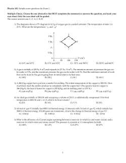


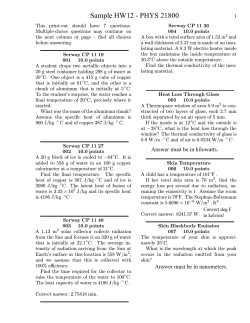


© Copyright 2026