
Monolithic Amplifier GVA-123+ Flat Gain, Ultra-Wideband
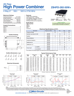
Flat Gain, Ultra-Wideband Monolithic Amplifier 50Ω GVA-123+ 0.01 to 12 GHz The Big Deal • Ultra broadband performance • Excellent Gain Flatness • Broadband without external matching components SOT-89 PACKAGE Product Overview GVA-123+ (RoHS compliant) is an advanced ultra-wideband amplifier fabricated using GaAs HBT technology and offers excellent gain flatness over a broad frequency range. In addition, the GVA-123+ has good input and output return loss over this frequency range without the need for external matching components. Lead finish is tin-silver over nickel. It has repeatable performance from lot to lot and is enclosed in a SOT-89 package for very good thermal performance. Key Features Feature Advantages Ultra Broad Band: 0.01 to 12 GHz Broadband covering primary wireless communications bands: Cellular, PCS, LTE, WiMAX in a single amplifier. Ultra Flat Gain ±0.7 dB typ: 0.05 - 8 GHz Ultra Flat Gain, eliminates need for compensation networks to achieve published results No External Matching Components Required GVA-123+ provides good Input and Output Return Loss of 12-28 dB over 0.05 - 6 GHz without the need for any external matching components Excellent ESD HBM: class 1C (1000 to <2000V) MM: class M2 (100 to <200V) Simplifies ESD handling. Notes A. Performance and quality attributes and conditions not expressly stated in this specification document are intended to be excluded and do not form a part of this specification document. B. Electrical specifications and performance data contained in this specification document are based on Mini-Circuit’s applicable established test performance criteria and measurement instructions. C. The parts covered by this specification document are subject to Mini-Circuits standard limited warranty and terms and conditions (collectively, “Standard Terms”); Purchasers of this part are entitled to the rights and benefits contained therein. For a full statement of the Standard Terms and the exclusive rights and remedies thereunder, please visit Mini-Circuits’ website at www.minicircuits.com/MCLStore/terms.jsp Mini-Circuits ® www.minicircuits.com P.O. Box 350166, Brooklyn, NY 11235-0003 (718) 934-4500 [email protected] Page 1 of 5 Flat Gain, Ultra-Wideband Monolithic Amplifier 0.01-12 GHz Product Features • Excellent Gain Flatness, ±0.7 dB, 0.05-8 GHz • Gain, 16.9 dB typ. at 2 GHz • Excellent return loss, 20 dB typ., 2 GHz CASE STYLE: DF782 PRICE: $5.95 ea. QTY. (10) Typical Applications • Base station infrastructure • Test instruments • MMDS & Wireless LAN • LTE • Satellite communication • Avionics GVA-123+ +RoHS Compliant The +Suffix identifies RoHS Compliance. See our web site for RoHS Compliance methodologies and qualifications General Description GVA-123+ (RoHS compliant) is an advanced ultra wideband amplifier fabricated using GaAs HBT technology and offers a broad frequency range. In addition, the GVA-123+ has good input and output return loss over this frequency range without the need for external matching components. Lead finish is tin-silver over nickel. It has repeatable performance from lot to lot and is enclosed in a SOT-89 package for very good thermal performance. simplified schematic and pin description 3 RF-OUT & DC-IN RF-OUT and DC-IN RF-IN 2 GROUND 4 1 RF-IN GND Function Pin Number RF IN 1 RF input pin. This pin requires the use of an external DC blocking capacitor chosen for the frequency of operation. RF-OUT and DC-IN 3 RF output and bias pin. DC voltage is present on this pin; therefore a DC blocking capacitor is necessary for proper operation. An RF choke is needed to feed DC bias without loss of RF signal due to the bias connection, as shown in “Recommended Application Circuit”, Fig. 2 GND 2,4 Description Connections to ground. Use via holes as shown in “Suggested Layout for PCB Design” to reduce ground path inductance for best performance. Notes A. Performance and quality attributes and conditions not expressly stated in this specification document are intended to be excluded and do not form a part of this specification document. B. Electrical specifications and performance data contained in this specification document are based on Mini-Circuit’s applicable established test performance criteria and measurement instructions. C. The parts covered by this specification document are subject to Mini-Circuits standard limited warranty and terms and conditions (collectively, “Standard Terms”); Purchasers of this part are entitled to the rights and benefits contained therein. For a full statement of the Standard Terms and the exclusive rights and remedies thereunder, please visit Mini-Circuits’ website at www.minicircuits.com/MCLStore/terms.jsp Mini-Circuits ® www.minicircuits.com P.O. Box 350166, Brooklyn, NY 11235-0003 (718) 934-4500 [email protected] REV. A M148071 GVA-123+ TH/RS/CP 140918 Page 2 of 5 GVA-123+ Monolithic InGap HBT MMIC Amplifier Electrical Specifications at 25°C and Vcc=5V, R= 16.5Ω unless noted Parameter Condition (GHz) Frequency Range Gain 0.05 0.85 2.0 6.0 8.0 10.0 12.0 0.05-8 0.05 0.85 2.0 6.0 8.0 10.0 12.0 0.05 Output Return Loss 16.2 17.2 16.9 16.4 16.3 12.5 7.1 ±0.7 12.7 24.9 23.8 22.2 9.2 7.5 6.3 14.4 15.2 16.0 0.85 2.0 6.0 8.0 10.0 12.0 6.0 0.05 0.85 2.0 6.0 8.0 10.0 12.0 0.2 0.85 2.0 6.0 8.0 10.0 12.0 0.2 0.85 2.0 6.0 8.0 12.0 Reverse Isolation Output Power at 1dB Compression Output IP3 Noise Figure Supply Operating Voltage (Vcc) Device Operating Current Device Current Variation vs. Temperature2 Device Current Variation vs. Voltage Thermal Resistance, junction-to-ground lead (2) Typ. 0.01 Gain Flatness Input Return Loss (1) Min. 31.0 23.5 15.5 9.0 7.4 6.0 20.7 15.9 16.3 16.2 13.4 10.3 7.4 5.1 30.2 31.1 29.9 24.5 21.8 19.1 14.9 3.8 3.9 4.0 4.4 4.9 6.9 5.0 52 56 0.020 156 4.8 Max. Units 12.0 GHz dB 18.6 dB dB dB dB dBm dBm dB 5.2 57 V mA µA/°C mA/mW °C/W Measured on Mini-Circuits Characterization test board TB-665+. See Characterization Test Circuit (Fig. 1) (Current at 85°C — Current at -45°C)/130 Absolute Maximum Ratings(3) Parameter Ratings Operating Temperature (ground lead) Storage Temperature Operating Current at 5V (Vcc) & 16.5Ω resistor Power Dissipation Input Power (CW) DC Voltage on Pin 3 -40°C to 85°C -65°C to 150°C 100 mA 0.34 W 28 dBm (5 min max.) 11 dBm (continuous) 6V (3) Permanent damage may occur if any of these limits are exceeded. Notes A. Performance and quality attributes and are conditions not expressly stated in normal this specification document are intended to be excluded and do not form a part of this specification document. Electrical maximum ratings not intended for continuous operation. B. Electrical specifications and performance data contained in this specification document are based on Mini-Circuit’s applicable established test performance criteria and measurement instructions. C. The parts covered by this specification document are subject to Mini-Circuits standard limited warranty and terms and conditions (collectively, “Standard Terms”); Purchasers of this part are entitled to the rights and benefits contained therein. For a full statement of the Standard Terms and the exclusive rights and remedies thereunder, please visit Mini-Circuits’ website at www.minicircuits.com/MCLStore/terms.jsp Mini-Circuits ® www.minicircuits.com P.O. Box 350166, Brooklyn, NY 11235-0003 (718) 934-4500 [email protected] Page 3 of 5 GVA-123+ Monolithic InGap HBT MMIC Amplifier Characterization Test Circuit Fig 1. Block Diagram of Test Circuit used for characterization. (DUT soldered on Mini-Circuits Characterization test board TB-665+) Gain, Return loss, Output power at 1dB compression (P1 dB) , output IP3 (OIP3) and noise figure measured using Agilent’s N5242A PNA-X microwave network analyzer. (R=16.5Ω) Conditions: 1. Gain and Return loss: Pin= -25dBm 2. Output IP3 (OIP3): Two tones, spaced 1 MHz apart, 0 dBm/tone at output. Recommended Application Circuit Fig 2. Test Board includes case, connectors, and components soldered to PCB (Cblock=0.001 µF, Cbypass=0.1 µF, R=16.5Ω) Product Marking V123 Notes A. Performance and quality attributes and conditions not expressly stated in this specification document are intended to be excluded and do not form a part of this specification document. B. Electrical specifications and performance data contained in this specification document are based on Mini-Circuit’s applicable established test performance criteria and measurement instructions. C. The parts covered by this specification document are subject to Mini-Circuits standard limited warranty and terms and conditions (collectively, “Standard Terms”); Purchasers of this part are entitled to the rights and benefits contained therein. For a full statement of the Standard Terms and the exclusive rights and remedies thereunder, please visit Mini-Circuits’ website at www.minicircuits.com/MCLStore/terms.jsp Mini-Circuits ® www.minicircuits.com P.O. Box 350166, Brooklyn, NY 11235-0003 (718) 934-4500 [email protected] Page 4 of 5 GVA-123+ Monolithic InGap HBT MMIC Amplifier Additional Detailed Technical Information additional information is available on our dash board. To access this information click here Data Table Performance Data Swept Graphs S-Parameter (S2P Files) Data Set (.zip file) Case Style DF782 (SOT 89) Plastic package, exposed paddle, lead finish: tin- Tape & Reel F55 Standard quantities available on reel 7” reels with 20, 50, 100, 200, 500 or 1K devices Suggested Layout for PCB Design PL-370 Evaluation Board TB-781+ (0.05 - 10 GHz) Environmental Ratings ENV08T1 silver over nickel ESD Rating Human Body Model (HBM): Class 1C (1000 to <2000V) in accordance with ANSI/ESD STM 5.1 - 2001 Machine Model (MM): Class M2 (100 to <200V) in accordance with ANSI/ESD STM5.2-1999 MSL Rating Moisture Sensitivity: MSL1 in accordance with IPC/JEDEC J-STD-020D MSL Test Flow Chart Start Visual Inspection Electrical Test SAM Analysis Reflow 3 cycles, 260°C Soak 85°C/85RH 168 hours Bake at 125°C, 24 hours Visual Inspection Electrical Test SAM Analysis Finish Additional Notes A. Performance and quality attributes and conditions not expressly stated in this specification document are intended to be excluded and do not form a part of this specification document. B. Electrical specifications and performance data contained in this specification document are based on Mini-Circuit’s applicable established test performance criteria and measurement instructions. C. The parts covered by this specification document are subject to Mini-Circuits standard limited warranty and terms and conditions (collectively, “Standard Terms”); Purchasers of this part are entitled to the rights and benefits contained therein. For a full statement of the Standard Terms and the exclusive rights and remedies thereunder, please visit Mini-Circuits’ website at www.minicircuits.com/MCLStore/terms.jsp Notes A. Performance and quality attributes and conditions not expressly stated in this specification document are intended to be excluded and do not form a part of this specification document. B. Electrical specifications and performance data contained in this specification document are based on Mini-Circuit’s applicable established test performance criteria and measurement instructions. C. The parts covered by this specification document are subject to Mini-Circuits standard limited warranty and terms and conditions (collectively, “Standard Terms”); Purchasers of this part are entitled to the rights and benefits contained therein. For a full statement of the Standard Terms and the exclusive rights and remedies thereunder, please visit Mini-Circuits’ website at www.minicircuits.com/MCLStore/terms.jsp Mini-Circuits ® www.minicircuits.com P.O. Box 350166, Brooklyn, NY 11235-0003 (718) 934-4500 [email protected] Page 5 of 5


© Copyright 2026