
Ultra Narrow Band Modulation Textbook Harold R. Walker
Ultra Narrow Band Modulation Textbook Harold R. Walker Pegasus Data System, Additions and corrections are made frequently. November 1, 2014 No manuscript is ever perfect. Please report any errors and suggested corrections to <[email protected]> 1 Contents: Preface Chapter 1 Chapter 2 Chapter 3 Chapter 4 Chapter 5 Chapter 6 Chapter 7 Chapter 8 Chapter 9 Chapter 10 Chapter 11 Chapter 12 Chapter 13 Chapter 14 Chapter 15 Chapter 16 Chapter 17 Chapter 18 Baseband Coding Modulation Methods Filter Effects Filters with Group Delay Bipolar Phase Shift Keying and Coded BPSK Abrupt Phase Change Modulation Methods Negative Group delay Pulse Position Phase Shift Keying Modulation with Broad Pulses Circuitry for Modulation and Detection Sideband and Carrier Vectors Unnecessary Sidebands and Grass Signals plus Interference Measuring Bit Error Rate Shannon’s Channel Capacity and BER Doppler Effects and AFC Multipath Effects Amplitude Pulse Modulation Systems Appendices: 1) Universal Resonance Curve 2) Fourier Analysis 3) Measured Effects of Abrupt Phase Change Modulation 4) Demonstrated Applications 5) Filter overload 6) Bessel Sidebands 7) Abrupt Phase Change Modulation Analysis Cover: Power Spectral Density of Ultra Narrow Band Modulation. 2 Preface Ultra Narrow Band Modulation was conceived in 1985 as a method to be used with ’FM Sub-Carriers’ ( as opposed to ‘FM Supplementary Carriers’, or ‘In Band On Channel’ Carriers ). In its original form, data rates as high as 196 kb/s were obtained from a subcarrier at 98 kHz. A pulse width modulation baseband encoding method called the “Slip Code” was used. Descriptions of this method are given in the references. That method, which was basically a baseband method, was limited in data rate and required excessive filtering, which precluded it from being a practical Ultra Narrow Band method. Bandwidth efficiencies as high as 15 bits/sec./Hz were being achieved. References: [A][B]. An improved method known as “Very Maximum Sideband Modulation” [C][E] was introduced in 1996. This newer method resulted in a suppressed carrier plus numerous sidebands, only one of which needed to be transmitted. All other sidebands were removed by filtering. The single sideband transmitted was a single frequency with no measurable bandspread due to the pulse width modulated baseband coding method used. Under those conditions, the bandwidth efficiency was equal to the data rate. The transmission method employed was ‘Single Sideband- Suppressed Carrier’ ( SSB-SC ). The pulse width modulation code used was referred to as the “Aperture Code”. Dividing the aperture code by two resulted in a significant improvement. There were thus two VMaxSK modes- VMSK/1 and VMSK/2. One important feature was noted using this method, in that the suppressed carrier did not have to be restored for detection. All the necessary information required for detection was present in a single sideband alone, which was a single frequency containing the phase reversal modulation. Since all other sidebands, harmonics and the carrier were removed, this was a single frequency method requiring only 1 Hz of transmitted bandwidth. It was noted while developing circuits for VMSK/2 that a similar result could be obtained by abrupt phase change modulation of a carrier, if the filters used had zero group delay. The mathematical precedent for this was published by Howe in 1939. Since a family of near zero group delay filters had been developed for VMSK/2, this presented no problem. The newer method using ‘Abrupt Change Phase Reversal Keying’ of the carrier was developed ( ACPRK ), and released as a possibly marketable product in 2001.[D]. The transmitted signal is a single frequency, which contains no useful sidebands, yet contains abrupt changes of phase, up to and including +- 90 degrees, as in BPSK modulation. Bipolar Phase Shift Keying ( BPSK with +- 90 degree modulation ) has a serious problem in its realization, in that it requires a restored carrier, which can be ambiguous. The data pattern is recognizable, but the ones and zeros can be interchanged, or the data can be said to be inverted. For this reason, ‘differential coding’ is used, which causes a loss of 2 dB in the resulting signal to noise ratio for a given Bit Error Rate. 3 Abrupt phase change modulation does not have this problem if +- 45 degree modulation is used instead of +- 90 degrees. It has been shown there need not be a loss in the SNR when this is done. For example BPSK and QPSK have the same theoretical SNR for a given BER, yet one uses +-90 degrees and the other +-45 degrees. The ambiguity can also be avoided by using a baseband code other than NRZ with full bit periods. For example the RZ baseband code can be used. There have been as many as a dozen or more proposed methods to achieve modulation without useful sidebands. Some are listed in the ‘Papers and Patents’ references. Some have been patented. As of early 2007, the most successful methods are ‘Pulse Position Phase Reversal Keying’ ( 3PSK) and Non Return to Zero Minimum Sideband. (NRZ-MSB). The VMSK/2 method was evaluated by Dr W.C.Y. Lee at Vodaphone, ( 40 ) who states: “VMSK can also be used. It can send a 48 kb/s data stream through a 2 kHz bandpass filter and receives with good quality. The idea is to find ways to slightly mark the states of the modulation on the carrier wave such that less distortion of the carrier waveform can be achieved. Of course we know that an undistorted CW carrier only needs a 1 Hz filter bandwidth in principle.” Dr. Lee was actually evaluating a 273 kb/s data rate in a 30 kHz channel allocation for prospective cellular phone use. [C]. This method was also evaluated by Bell South with positive comments. This 1 Hz filter statement is true for all ‘Ultra Narrow Band’ methods, if it is accepted that the transmitted signal is a single frequency bearing phase modulation without useful sidebands. However, that single frequency must contain periods of abrupt phase change from 90 to 180 degrees, lasting as short a period as one IF cycle and as long as one or more bit periods, as was disclosed by Prof. Howe in the paper published in "Wireless Engineer", Nov. 1939. pp 547. There is one important characteristic which is holding up widespread adoption of Ultra Narrow Band modulation, and that is the filters. There is no known way to ultra narrow band filter ‘Ultra Narrow Band’ modulation at baseband. At the RF level, the filters are complex and must be hand tuned. There is no known way at this time to build a zero group delay narrow band filter into a DSP, FIR or IIR filter. The author wishes to thank Drs. C.S. Koukourlis and J.C. Pliatsikas, at Demokritos University, Greece, Dr. J.N. Sahalos at Aristotle University, Greece, Dr. Kamilo Feher at University of California, Davis, Dr. Saso Tomazic, University of Ljubljana, Slovenia, Dr Mike Zierdt at Bell labs, and Dr Lenan Wu at S.E. University Nanjing, China, for their contributions. It is hoped the users will inform the author of any errors found so that they be corrected. Harold R. Walker: BS, BSEE, MSEE, PE. The author’s past experience includes serving as Head of the Infra Red Laboratory at the Naval Air Research and Development Center, as Vice President of Blonder-Tongue Labs - a Cable TV manufacturer, and Director of Research at the ‘Educasting’ subsidiary of GTE/Sylvania. 4 He has taught as Adjunct Professor at the University of Tennessee, and at the New York Institute of Technology. As a lecturer for Besser Associates, he has taught Wireless Systems Design courses at Lucent Technologies, National Semiconductor University and Hewlett Packard. He has also guest lectured at Princeton University, Villanova University, De La Salle University, Manila, and S.E. University, Nanjing, PRC. He has presented numerous technical papers and holds more than 40 patents. Papers and Patents Relating to Ultra Narrow Band Modulation: 1) H.R. Walker, A Facts About High Speed SCA Data Transmission", Proceedings of the 1988 Broadcast Engineering Conference, Society of Broadcast Engineers, Denver Col.1988. 2) H.R. Walker, ADigital Audio for Links and Subcarriers" 43 rd Annual Broadcast Engineering Proceedings, National Association of Broadcasters, April 28, 1989, Las Vegas, Nev. 3. H.R. Walker, " Field Experience With VPSK Digital STL " Proceedings of the Broadcast Engineering Conference 1992 " Society of Broadcast Engineers , pp 66-73. 4) H.R. Walker, A Digital Modulation using Single Sideband FM with VPSK Encoding Reduces Bandwidth 10/1", Proceedings R.F. Expo East, Baltimore, Md. Aug. 21, 1995 5) B. Stryzack and H.R. Walker ", Improve Data Transmission Using Single Sideband FM with Suppressed Carrier", R.F. & Microwaves Magazine, Nov. 1994 (Wireless Systems Designs Supplement) 6) B.Stryzak and H.R. Walker, A Digital Cordless Telephone Provides WLAN/ Telephone/ Video phone Service", Fourth Wireless Symposium, Santa Clara Cal., Feb. 1996. ( The paper describes a Cordless Phone for 46/47 MHz that can handle Videophone traffic at 320 Kb/s -15 bits/sec/Hz compression). 7) H.R. Walker, A The Advantages of VPSK Modulation", Transactions -IEEE Wescon, Communications Technology, Part 1., San Francisco, Cal., Nov. 1995. 8) B.Stryzak and H.R. Walker, A U-PCS Band Wireless PBX / LAN is Multimedia Ready, Fourth Wireless Symposium, Santa Clara Cal., Feb. 1996. ( Using VPSK for Wireless LANs ). 9) H.R. Walker, A A Summary of Digital Modulation Techniques". Wireless Technology Conference and Exposition, Providence R.I. Oct. 7, 1996. 10) B. Stryzak, ADigital Data Transmission at 15 Bits/Sec/Hz" Wireless Technology Conference and Exposition, Providence R.I. Oct. 7, 1996. 11) H.R. Walker, AVPSK Modulation Transmits Digital Audio at 15 Bits/Sec/Hz". Microwaves and RF Magazine, Wireless Design Supplement. Dec. 1996. 12) B. Stryzak and H.R. Walker, A VPSK Modulation on FM Subcarriers@, Wireless Symposium, Santa Clara Cal. Feb. 1997. 13) H. R. Walker, A High Data Rate Power Line Modem@ Wireless Symposium, Santa Clara Cal. Feb. 1997. New Modem using VMSK modulation. 14) H.R. Walker, A VPSK and VMSK Modulation Transmit Digital Audio and Video at 15 Bits/Sec./Hz.@ IEEE Transactions on Broadcast Engineering, March 1997. 15) H.R. Walker, A VPSK Modulation, A Tutorial@, Conference Proceedings, RF Expo West, San Diego, Cal. Jan 29, 1995 16) H.R. Walker, A Digital Cordless Telephone Provides WLAN/ Telephone/ Video phone Service@, Applied Microwaves and RF Magazine, Jan./Feb. 1997. ( Describes a Cordless Phone for 46/47 MHz that can handle Videophone traffic at 320 Kb/s -15 bits/sec/Hz compression- using VPSK modulation). Can now do 1.544 Mb/s using VMSK/2 and 5.0 Mb/s using NRZMSB. 17) H.R. Walker, A Comparison of FM vs VPSK Modulation in RPU Service@, IEEE 44 th Annual Broadcast Symposium. IEEE Broadcast Technology Society, Wash. D.C., 1994 18) H.R. Walker, @Encyclopedia of Electrical and Electronics Engineering@ John Wiley, NYC. Section Author on A Intermediate Frequency Amplifiers@, Vol. 11, Edited by Prof. John Webster, U. of Wisconsin. 19) H.R. Walker. , @Encyclopedia of Electrical and Electronics Engineering,@ John Wiley, NYC. Section Author on "Modulation Analysis@. Vol. 13. 20) H.R. Walker, AVMSK, A New Modulation Concept@, Wireless Technology Conference, Chantilly, Va. Oct. 7, 1997. 5 21) H.R. Walker, AVMSK, A New Modulation Method@, Wireless Symposium, East, Burlington, Mass. Sept 15, 1997. 22) H.R. Walker, A Universal Equation Analyzes All Modulation Methods, Applied Microwaves and RF. July/Aug. 1997. This paper also appears as -- "Modulation Analysis", H.R. Walker, @Encyclopedia of Electrical and Electronics Engineering", John Wiley, NYC, Vol. 13. 23) H.R. Walker, A Attain High Bandwidth Efficiency Using VMSK Modulation@, Microwaves and RF Magazine, Dec. 1997. 24) H.R. Walker, “High Data Rate Power Line Modem uses Biphase Modulation”, Proceedings Fifth Annual Wireless Symposium, Santa Clara Convention Center , 1997. 25) J. Pliatsikas, C. Koukourlis, J. Sahalos and H.R. Walker, A VMSK Modulation BOOSTS Wireless Communications Efficiencies@, Wireless Systems Design Magazine, Jan 1998. 26) H.R. Walker, B.Stryzak, and Mildred Walker, @VMSK Modulation, A Tutorial”. Wireless Symposium, Santa Clara Ca. Feb. 12, 1998 27) Dr. C.S. Koukourlis, J.C. Pliatsikas, Dr. J.N. Sahalos and H.R. Walker, A Spectrally Efficient Biphase modulation.@ Applied Microwave and Wireless Magazine. May 1998. 28) J.C. Pliatsikas, C.S. Koukourlis, J.N Sahalos, H.R. Walker, "Digital Implementation of Alternate Aperture Phase Shift Keying Modulation (AAPSK)", Proceeding ICT 98, Chalkidiki Greece, June 1998. ( Different name for VMSK ). 29) H.R. Walker, Dr. J. Pliatsikas, Dr. C Koukourlis and Dr. J. Sahalos, "Wireless Communications Using Spectrally Efficient VMSK/2 Modulation" In "Third Generation Mobile Telecommunication Systems" Springer Verlag, Berlin, Edited by Dr. P. Stavroulakis. 30)H.R. Walker, @Encyclopedia of Microwave and Electronic Engineering John Wiley, NYC. Section Author on Intermediate Frequency Amplifiers. Edited by Prof. Kai Chang, Texas A&M. 31) H.R. Walker, "Understanding Ultra Narrow Band Modulation", Microwaves and RF Magazine, Dec. 2003. 32) H.R. Walker, "MSB Modulation Doubles Cable TV and FM-SCA Capacity" IEEE CCNC2004, Las Vegas NV. Jan 2004. 33) H.R. Walker, "Ultra Narrow band Modulation", Wireless Systems Design Conference, San Diego CA, March 8, 2004. 34) H.R. Walker, "Ultra Narrow Band Modulation" , IEEE Sarnoff Symposium, Princeton NJ, April 26, 2004. 35) H.R. Walker, "Ultra Narrow Band Modulation". International Conference on Computing, Communications and Control Technologies, CCCT2004. 36) Bohdan Stryzak, "Comparing Ultra Wideband and Ultra Narrow Band Modulation", Wireless Systems Design Conference, San Diego CA, March 8, 2004. 37) H.R. Walker and Bohdan Stryzak, "Comparing Ultra Wideband and Ultra Narrow Band Modulation" ". International Conference on Computing, Communications and Control Technologies, CCCT2004. Austin Tx. 38) Wang Jianqing, Yu Xiaoyan, Si Hongwei, Wu Lenan, “ Performance Evaluation of LDPC Coded VWDK Modulations” International Conference on Computing, Communications and Control Technologies, CCCT2004. 39) Wang Jianqing, Si Hongwei, Wu Lenan, Li Xiaoping, “ Optimization of VWDK PSD and its Performance”, International Conference on Computing, Communications and Control Technologies, CCCT2004. Austin Tx. 40) Li Xiaoping, Si Hongwei, Wu Lenan, “ On Spectrum Structure and Optimization of VWDK Modulated Waveforms”, International Conference on Computing, Communications and Control Technologies, CCCT2004. Austin Tx. 41) Wm. C.Y. Lee, “Lee’s Essentials of Wireless Communications”, McGraw Hill 2001. 42) K. H. Saywood and Lenan Wu, "Raise Bandwidth Efficiency with Sine-WaveModulation VMSK". Microwaves and RF Magazine, April 2001. 43) Li Xiaoping and Wu Lenan,“Power Spectra Analysis for a standard sine-like VMSK modulation”, Chinese Journal of Radio Science, Dec. 2003. 44) Li Xiaoping and Lenan Wu, “On Orthogonality of Sine-Like VMSK Modulations”, Journal of Circuits and Systems, ( Chinese ). 6 45) J.S. Lin, K. Feher, “Ultra High Spectral efficiency Feher Keying (FK): Computer Aided Design and Hardware Development”, European Test and Telemetry Conference 2001, Marseilles France June 2001. 46) J.S. Lin, K. Feher, “Test and Evaluation of Ultra High Spectral efficiency Feher Keying (FK)”, Proceedings of International Telemetry Conference, Las Vegas NV, Oct 2001. 47) A. Fikry, “Code Division Multiple Access System Based on Chaos Spreader and VMSK Modulation”, ATNAC2003, available http://atnac2003.atcrc.com/POSTERS/Fikry.pdf 48) C. Koukourlis, “ Data Transmission Over Analog TV Broadcasting”, International Journal on Communications Systems, April 2008. http://www3.interscience.wiley.com/journal/117946196/grouphome/home.html 49) J.C. Pliatsikas, C.S. Koukourlis, J.N. Sahalos, “On the Combining of Amplitude and Phase Modulation in the same Signal”. IEEE Transactions on Broadcasting, June 2005. 50) H.R. Walker, “Modulation without Useful Sidebands”, 11 th World Conference on Systematics, Cybernetics and Informatics WMSCI 2007. Orlando FL. July 2007. 51) Chenhao Qi and Lenan Wu, "Hybrid Modulation for AM Broadcasting". The 3rd International Conference on Natural Computation (ICNC'07). Hainan, China. August 2007. 52) Rumin Yang, Chengbo Yu, Xinyu Yu, Zheng Zhou, “ Combination of Conventional AM with UWB Impulse Radio: A UNB Solution for Next Generation of Communications”, submitted IEEE Globecom 2007 Wireless Communications. (53) Xiaoping Li and Lenan Wu, “Power Spectra Analysis for A Standard Sine-like VMSK Modulation”, Chinese Journal of Radio Science, Vol. 18, No. 6, 2003, pp. 722-726. (54) Xiaoping Li and Lenan Wu, “On Orthogonality of Sine-like VMSK Modulations”, Journal of Circuits and Systems, Vol 9, No. 4, 2004 (Chinese). (55) Lenan Wu, “UNB Modulation in High Speed Space Communications”, Second International Conference on Space Information Technology ( ICSIT’2007 ), Wuhan China. (56) Lenan Wu, “Advances in UNB High Speed Communications”, Progress in Natural Science, 17(10),143-149(2007). (57) Lenan Wu, “UNB Transmission and Compact Spectral Communications”, Telecom Letters, 2, 16(2004), in Chinese. (58) Deng Xiao-tao, Gao Jun, Lin jing-na, “Shannon limit explanation of the UNB modulation” Journal of Shandong University of Technology, 2007, (59) Feng Man and Wu Lenan, “Extension of Shannon’s Channel Capacity”( to UNB ), International Symposium on Intelligent Signal Processing and Communications Systems ( ISPACS 2007 ). (60)Yang Rumin, Hao Jianjun, Zhou Dengyi, and Zhou Zheng, “An Ultra Narrowband System for Next Generation of Wireless Communications”, Computer Science, 2007 Vol. 34, No. 9 (Special Issue), China. (61) Zhao Cheng-shi, Wang Shu-bin, Zhao Zheng, Kwak Kyung –Sap, “ Demodulation Performances of Two Sine Like Waves That Realize UNB”, ICC'08 - General Symposium ( submitted ). (62) C.V. Whaits, R.M. Braun, “Phase Errors in the Coherent Demodulation of VPSK and a Solution Using DSSS Modulation”. Research Group, University of Capetown, Dept. of Elect. Engineering, Private Bag Rondebosch, 7700, Capetown. (63) Man Feng, Lenan Wu. Extension to Shannon’s channel capacity —— The theoretical proof. Proc. of Sixth International Conference on Information, Communications and Signal Processing (ICICS 2007), P0189, (Dec. 10- 13, 2007) (64) Feng Man, Wu Lenan, and Wei Fufeng. Blind detection in VWDK systems via sequential Monte Carlo. Proc. of 2005 International Conference on Neural Networks & Brain (ICNN&B’05), Vol. 3, 100104(Oct. 13-15, 2005), (65) Zhonghui Mei, Lenan Wu, and Shiyuan Zhang. Joint detection for a bandwidth efficient modulation method. Proc.of 9th International Conference on Knowledge-Based Intelligent Information and Engineering System, Part Ⅲ,483-487 (September 14-16, 2005), Melbourne, Australia (Lecture Notes in Artificial Intelligence 3683) (R.Khosla, R. J. Howlett, and L. C. Jain (Eds.): KES2005, LNAI 3683, 483-487, 2005) (66) Zhu Renxiang, Wu Lenan. Quantum stochastic filters for nonlinear time-domain filtering of communication signals. Journal of Southeast University (English Edition), 23(1), 22-25(Mar. 2007) 7 (67) Chen-hao Qi, Man Feng and Le-nan Wu. Analysis of transmission system based on phase locked loop. Proc. of Third International Conference on Natural Computation (ICNC 2007), Vol. 2, 415-419 (24-27, August 2007), (68) Li Xiao-Ping, Wu Le-Nan. On Optimization of VWDK Modulated Waveforms. Journal of Electronics & Information Technology, 27(11) 1714-1716(2005) (in Chinese) (69) Qi Chen-Hao, Wu Le-Nan, and Zhang Shi-Yuan. AM broadcasting schemes based on compound modulation. JOURNAL OF APPLIED SCIENCES, 25(5), 451-455(2007.9) (in Chinese) (70) Qi Chen-Hao, Wu Le-Nan. PSD Analysis on AM Broadcasting using Hybrid Modulation. JOURNAL OF APPLIED SCIENCES, 25(6), 583-588(2007.11) (in Chinese) (71) Zhang Shi-Kai, Wu Le-Nan. Orthogonality and Power Spectra of EBPSK Modulated Waves. JOURNAL OF APPLIED SCIENCES, 26(2), 127-131(2008.3) (in Chinese) (72) Rastisla Rdka. The Utilization of VMSK at the Signa Transport by Means of XDSL Technologies.Eurocon 2001 Vol. 2, IEEE pp 450-453. (73) Zheng Guoxin, Very Minimum Chirp Keying as a Novel Ultra Narrow Band Communications Scheme. ICICS, Singapore, Dec., 2007. (74) Zheng Guoxin, Non DC Offset Very Minimum Chirp Keying Modulation as a Novel Ultra Narrow Band Communications Scheme, CCWMSN07 Proceedings,pp755 -758. Shanghai, 2007. (75) Chenhao Qi and Lenan Wu. Comments on “On the combining of the amplitude and phase modulation in the same signal”. IEEE Transactions on Broadcasting, vol. 54, no.3, Sept. 2008, p.489. ( 76) Zhang, Shi-kai, “Ultra Narrow Band Modulation Salvages Spectrum”, Microwaves and RF Magazine. April, 2009. pages 55 -60. ( 77) Wu, Lenan, Advance in UNB High Speed Communications, -Progress in Natural Science, ( In Chinese ), 2007: 17(10) pp 143-149. (78) Feng Man, Wu Lenan, Gao,P. An Impulse Filter method used in ABPSK signal. Chineewse patent Publishing, 200910029875.3. (79) Feng Man, Wu L.N., and Qi C.H. Analysis and Optimization of Power Spectrum on EBPSK modulation in Throughput Efficient Wireless System. Journal of South East University (English Edition ) -148. (80) Feng He, Wu Lenan, “Analysis of Power Spectrum of Continuous Phase Waveforms for Binary Modulation Communications”, IEEE-ICUMT 2009, St Petersburg Russia. (81) Feng Man, Lenan Wu, “ A Simulation Analysis of Anti-Interference Performance in EBPSK Systems”. IEEE-ICUMT 2009, St Petersburg Russia. (82) Shikai Zhang, Lenan Wu, “ Hybrid Modulation Based on Combining of AM and UNB, Journal of Convergeance Information Technology, Sept. 2009. (83) Man Feng, Lenan Wu, “ On BER Performance of EBPSK – Modem in AWGN Channel, Sensors 2010, www.mpdi.com/journal/sensors. (84) H.R. Walker, “Experiments in Pulse Communications with Filtered Sidebands”, High Frequency Electronics magazine, Sept. 2010, pp 64-68. www.highfrequencyelectronics.com. (85) H.R. Walker, “Sidebands are not Necessary”, Microwaves and RF Magazine, August 2011. pp72. (86) http://mwrf.com/systems/assessing-different-ultranarrowband-formats (87) http://www.springerlink.com/content/572qj4n357184052/ Textbook on UNB A search using IEEE Xplore ( ieeexplore.ieee.org ) is recommended for many papers not listed. Search under VMSK, UNB, EBPSK -- and under authors names of authors listed above. Additional topics from Google, Bing etc. are “Negative Group Delay”, “Wavelet RF Filters” and “Fourier Frequency Separation”. Applicable Patents: [A] US 4,742,532, H.R. Walker, A High Speed Data Communications System" ( 1 st VPSK Pat. [B] US 5,185,765, H.R. Walker, A High Speed Data Communications System" ( 2 nd VPSK Pat.) [C] US 5,930,303, H.R. Walker, A Digital Modulation Employing Single Sideband With Suppressed Carrier", covers VMSK and VMSK/2. [D] US 6,445,737, H.R. Walker, “Pulse Position Phase Reversal Keying ( 3PRK )”, also called Missing Cycle Modulation ( MCM/3PRK ). 8 [E] US 6,748,022, H.R. Walker, “Single Sideband Suppressed Carrier Digital Communication Method and System.” ( VMSK variation ). [F] US 6,775,324, Mohan, Riedl and Zhang, “Digital Signal Modulation System”, assigned to Thompson Licensing. ( Describes a method similar to ‘765 patent plus spread spectrum ) [G] US 6,198,777, K. Feher, "Ultra High Spectral Efficiency Feher Keying" ( FK ). [H] US 6,901,246 J.A. Bobier and N. Khan. “Suppressed Cycle Based Carrier Modulation Using Amplitude Modulation”, 2005. [I] US 6,968,014 J. A. Bobier, “Missing Cycle Based Carrier Modulation”, 2005 [J] US 7,424,065 H.R. Walker, , “Apparatus and Method for Ultra Narrow Band Wireless Communications ”, 9/9/2008. [K] H.R. Walker, US Pat. 7,268,638, “ Apparatus and Method for Data Rate Multiplication”. [L] H.R. Walker Application 11,807,077, published US2007-0237218-A1 “ Analog Mod. without Sidebands”. CIP included in US 7,424,065 above. [M] J.A. Bobier, US Pat. 7,486,715, “Narrow Band Integer Cycle or Impulse Modulation Spectrum Sharing Method”. [N] H.R. Walker, Japanese Patent 4215509, “Digital Modulation Device in a system and method of using same.” [O] Feher, Kamilo, US Pat. 7,421,004, “ Broadband,Ultra Wideband and Ultra Narrow Band Reconfigurable Interoperable Systems”, 9/2/2008. [P] J.A. Bobier, US Pat. 7,003,047, Tri State Integer Cycle Modulation” [Q] H.R. Walker, Provisional Filing, 61300973, “Method and Apparatus to Improve Pulse Modulation Systems. [R] D.L. West, Application US 2010/0074371 A1, 3/25/2010, Ultra Narrow Band Frequency Selector For Zero Point Modulated Carrier. CN1889550A ( Chinese Pat. ) L. Wu and S. Zhang, “A Unitive Method for Binary Phase Modulation and Demodulation”. CN03152978.X ( Chinese Pat. ) Wu Lenan et al, “A Modulation Method for High Efficient Utilization of Frequency Bandwidth”. 2003. The US PCT for MSB ( US 7,424,065 ) is US02/02943. The following information relates to US 6,445,737, Japanese # is 2002-564837 Chinese # is I I E 0 31971 Korean file7010450/2003 European filing is 02720881.8-2215. Filed in English. Translations in progress for Germany, Sweden, Finland, France Known Abandoned Methods: 4,742,532 A High Speed Data Communications System@ ( 1 st VPSK Pat.) 5,185,765 A High Speed Data Communications System@ ( 2 nd VPSK Pat.) "Time-Shift Keying" (TSK), ISD Communications. Quick Explanation of Ultra Narrow Band Modulation. 9 All Ultra Narrow Band modulation methods are end to end pulse width amplitude modulation methods. This is true of the earliest ( VPSK ) and the most recent NRZ-MSB codes. The modulator used abruptly switches the phase of the carrier to one phase for the digital ones and to a different phase for digital zeros. The angular difference can be from 180 degrees to 90 degrees or less, though a larger angle than 90 degrees may be preferred. The UNB methods do not differ from the well known ‘Binary Phase Shift Keying’ ( BPSK ) method, except for the special narrow bandpass filters used. VMSK is referred to as coded BPSK. NRZ-MSB is the same as standard BPSK except that the shifted phase angle with binary data is less than 180 degrees. The methods are analyzed as pulse amplitude modulation methods, just as BPSK is analyzed in all the texts. They do have a pulsed carrier which has shifted phase, which qualifies them as phase modulation when detected, but they remain basically amplitude modulation methods with end to end pulses on5 the different carrier phases.4 The spectrum seen is a Fourier spectrum typical of pulsed AM. 3 2 Sidebands that are created are in phase with the carrier and do not themselves cause any phase modulation change of the carrier itself, as is done in the Armstrong method to create PM. They can be removed as seen in Appendix 3. All sidebands merely change the amplitude of the carrier. 1 D AM AM Ph 1 C B A Ph 2 Fig. 1. The carrier is switched so as to cause Ph 1 or Ph 2 to be ON/OFF. The carrier for each phase is seen as Ph1 and Ph 2. The amplitude modulation sidebands from the ON/OFF switching are seen as contra rotating vectors that do not change Ph 1 or Ph 2. The sidebands, which are originally too strong, must be reduced by special filtering, or the method does not function without errors. Decreasing the carrier by 3dB relative to the sidebands causes near 50% errors. See Appendix A3. The sidebands must cause as little AM and PM as possible. This same plot is valid for BPSK, where the difference between Ph 1 and Ph2 is 180 degrees. Normally these sideband vectors are present so as to maximize the amplitude of the PH1 or Ph 2 vectors, or to cancel them entirely while the opposite phase is switched on. It can be shown that these Fourier sidebands are removable without loss of the pulse information. When a narrow band filter having near zero group delay is used with the pulses ( Chapter 7 ), the response in terms of phase shift and amplitude is nearly instantaneous so that the phase of the carrier is passed almost exactly like the phase of the carrier at the switched inputs to generate the modulation pulses. The ultra narrow band, near zero group delay filter, reduces the sideband levels to enable the method to meet FCC regulations to be classified as ‘Ultra Narrow Band’ modulation. A complete explanation of the end to end pulse width modulation with oscilloscope photos and spectrum analyzer plots is given in Appendix A3. If the phase change is retained in the carrier, without frequency change for the entire bit period, Fourier pulse sidebands can be removed. The components of a Fourier spectrum are separable if a negative or zero group delay filter is used. Title <Title> Size A Date: 5 4 3 Document Number <Doc> Sunday, January 07, 2007 2 The ’Nyquist Bandwidth’ for Ultra Narrow Band modulation is equal to the Intermediate Frequency. The ‘Transmission Bandwidth’ is 1 (one) Hz The ‘Noise Bandwidth’ is determined by the IF filter BW, which is typically 500 Hz. 10 Sheet 1 of 1 1 Chapter 1. Baseband Coding In order to transmit digital information in a useful manner, that is a manner in which it can be detected and decoded, the data clock and the data bits must be related in some manner so that they can be restored as transmitted. Feher ( 2 ) refers to most methods as Amodifications to the clock@, which can be interpreted to also mean the carrier according to Lee (18). There are only two useful alterations possible for UNB, 1) Amplitude, and 2) Phase. Frequency modulation of the clock ( carrier ) would be counter productive, since a steady recovered carrier frequency is needed at the output. “Baseband” can be defined as all those frequencies extending from 0 Hz to the highest frequency that needs to be passed prior to RF modulation. Generally, this is ½ the data clock rate. ( * See end note and Appendix A2 for Fourier and Nyquist analysis ). N RZ Data D ata Clock Zero D C Figure 1.1. The NRZ ( Non Return to Zero ) code is the starting code for all methods, since it defines the ones and the zeros in the digital pulse stream in varying pulse widths for the signal polarities as related to the data clock. With the NRZ code, one bit period equals one clock cycle. The baseband spectral frequencies transmitted extend from zero to 2 the clock frequency. Any spectral components beyond 2 clock frequency must be attenuated to comply with regulations that limit the allowable transmitted bandwidth. Nyquist (14) has shown that with ideal filtering, all the necessary energy is available within that bandwidth. Fig. 1.1a NRZI Encoding A variation of the NRZ code is the NRZI code. The phase reverses at the start of each digital one and makes no change for a digital zero, or the coding can be reversed, changing on the zeros. This method is also known as "differential coding". NYQUIST'S Bandwidth Theorem: Theorem: “If synchronous impulses, having a symbol rate of f s symbols per second, are applied to an ideal, linear phase brick wall filter, having a bandwidth = fs, the response to these impulses can be observed independently, that is, without inter-symbol interference”. (fs = 1/Ts). This criteria is referred to later as BT=1 or B=1/T. It is a very important relationship in Ultra Narrow Band Technology 11 Rephrased: If a filter is used having a rise time or envelop group delay Tg which is less than a pulse period, or symbol period Ts, the response to these impulses can be observed independently, that is, without intersymbol interference. Nyquist also shows that the maximum bandwidth required is equal to fs. Any energy outside this bandwidth can be eliminated without creating inter-symbol interference. This has always been interpreted to mean that the bandpass filter must have a bandwidth B equal to the symbol rate = 1/Ts. Or, in the case of BPSK, the data rate, which is ½ the clock rate. Some methods combine several bits into a symbol. ( MPSK, QAM, QPSK ). See note on page 24. "The power spectral density and the correlation function of a waveform are a Fourier transform pair", Taub and Schilling, [ 7 ] Chapter 1. The applicable baseband Fourier transform for an AM pulse is: An 2 AT Sin(n T / Ts ) Ts (n T / Ts ) ( For ODD functions ) See Appendix A2 for further details. Digitally coded signals can be analyzed at baseband using the Fourier Transform. At RF, the Fourier transform applies only to the sidebands, which can be removed by zero group delay filtering. There is a different treatment for the abruptly phase changed carrier. This equation results in two spectral components. A) A DC creeping level A(t/T), and B) A group of pulses spread over a wide frequency range. ( sinx/x pulses ). Nyquist further describes a filter meeting these criteria. However, other filters such as the common LC filter, or the Gaussian filters, can often be used. These filters are often used with a 3dB bandwidth less than the Nyquist bandwidth. They remove all sidebands other than the fundamental sideband, or first sideband pair. At baseband, a low pass filter is required, since the bandpass must extend from 0 Hz to ½ clock rate. Figure 1.2. The Baseband Spectrum ( Power Spectral Density ) for BiPhaseShiftKeying ( BPSK ) Modulation. From Feher (13) Figure 1.2 shows the spectrum for BPSK modulation. Without special filtering, the spectrum has significant 3/2, 5/2, and 7/2 harmonics and nulls at multiples of the bit rate, as predicted by the Fourier transform. With special filters, that is those meeting Nyquist’s criteria, these harmonics 12 Eq. 1.1 can be removed without affecting the data, as shown by the reduced sideband levels, since all of the useful data energy is in the fundamental lobe. BPSK modulation is the comparison standard against which all other methods are compared. The theoretical characteristics are B RF Bandwidth equals Bit Rate and the Eb/n for 10-6 Bit Error Rate ( BER ) is 10.5 dB. ( Discussed in Chapter 14 ). The NRZ ( Non Return to Zero ) data is shown in the format that is used within the computer, or other data source, in Fig. 1.1. A digital one is shown as a high level and a digital zero as a low level. This method creates a 'DC Creep', or 'Wander' ( Bellamy, (6)), which has plagued designers since digital transmission and magnetic recording were first used. As the high and low levels vary over a time period according to the data pattern, the average DC voltage also varies. To remove the DC voltage and permit transmission through transformers, the original positive swing from zero volts to a higher voltage is replaced with positive and negative voltage swings. ( zero DC in Fig. 1.1 ). However, some DC Creep is still there. Various changes have been suggested for the data pulse shape to reduce the DC Creep. An interesting change occurs in the spectrum when a change in the baseband code is introduced. Fig. 1.3 shows the RZ ( Return to Zero ) code. The polarity, or phase, is changed for one half clock period for each digital one only. The data bearing pulse widths are changed. This method does not correct for DC Creep. N RZ Data D ata Clock Return to Zero Figure 1.3 Return to Zero ( RZ ) Baseband Code. Data In 1 3 RZ Out 2 Fig. 1.4. RZ Generator. Clock In The baseband code contains abrupt phase changes at the edges. This code can be applied directly to a wire line, or phase modulator, and transmitted. Why isn’t this done? There are too many harmonics, plus the DC Creep, or offset, that varies with the data pattern. ‘DC Creep’ does not have any effect on the phase change edges in the pattern [ Ref. Bellamy ( Fig 4.6)( 6 )]. A full mathematical analysis using the Fourier transform is given in Appendix A2. The power spectral density ( PSD ) of Fig. 1.2 comes from the EVEN Fourier series for a rectangular pulse, which expanded is: y(t) = Apeak(t/Tp) [ ½ +(2/π)cosθ – (2/2π)cos2θ + (2/3π)cos3θ - (2/4π)cos4θ + (2/5 π)cos5θ ---] θ = nπ(t/Tp) Aav = Apeak(t/Tp) 13 where t is pulse ON time and Tp is one cycle period ( one on plus one off period ). ( This expansion is given in detail in Appendiz 2 ). Note that it has harmonics and nulls with various values of n as shown in Fig.1.2 -- with levels of: ( 2/, 2/2), (2/3), (2/4) --, which can be filtered off as shown in Fig. 1.2. This is an EVEN Fourier function. Some data patterns may have ODD harmonics instead of EVEN harmonics, depending on (t/Tp). See Appendix 2. Note also, the Aav term. This is an amplitude term that varies with the signal time spent above or below an average DC level according to the data pattern (t/Tp). It is the mathematical expression for the DC Creep. It is a term that must be dealt with in practice and removed if possible when using pulse modulation at RF. It may carry over into phase modulation as a noise vector. With no modulation present, or with a fixed data pattern, it has no varying level when using a balanced modulator. This integrated amplitude variation term was noted years ago with double density disk recording using the Miller code. ( MFM ). It was given the name "DC Wander”, or “DC Creep" and has nothing to do with the digital data recovery, except that it is best to remove it. Many patents have been granted on methods to do so. It is referred to on the following pages as "grass" from the RADAR term for noise. Current FCC terminoogy is “Interference Temperature”. The Fourier products arising from the pulse width modulation beyond the desired fundamental are unacceptable to the regulatory authorities and hence must be reduced, or removed, with pulse shaping filters. As Nyquist has shown, and as will be shown later, these harmonic sidebands are not necessary with UNB modulation. A complete Fourier analysis is given in Appendix A2. To remove these sidebands, a bandwidth limiting filter is required as in Fig. 1.2, where a Feher FBPSK-K filter was used. At baseband, it is a low pass filter having a shaped response. Some other shaped responses are seen in Fig. 1.2 N RZ Data D ata Clock Manchester ( Ethernet ) Figure 1.5. The Manchester Code Used with Ethernet. The Manchester code used with Ethernet is another code used to reduce the ‘DC Creep’. This is a widely used method for wireless LANs and in some short range wireless transmission methods. The difference between a one and zero is in the polarity of the change relative to the clock. The method utilizes the data clock and NRZ data in combination. The encoding device is a simple XOR gate. Data In 1 3 Manchester Out 2 Clock In Figure 1.6. Manchester Encoder. 14 Coded BPSK: Coded BPSK is a baseband code that has been used in the past with VMaxSK. Assume a square wave is transmitted using phase modulation that has equal time on phase one and phase two. A data pattern of 010101010 would have this characteristic. The spectrum has a single fundamental frequency at the clock frequency, plus all odd harmonics, as predicted by the Fourier series. ( Eq. 1.2 above ). This modulation pattern does not convey any useful information, Clock Clock Late Early Late Early Late Early VMSK/1 VMSK/2 Figure 1.7. Coded BPSK. By changing the timing of the square wave edges to indicate ones and zeros, the waveform can be made to convey intelligence ( pulse width modulation ). If the change is less than 1/5 of the clock period, the single frequency sideband characteristic desired for Ultra Narrow Band use is retained. Typically, changes less than 1/8 clock period were used. An improvement was made by Dr. J. Pliatsikas, who proposed dividing the baseband waveform by 2. This is shown above as VMSK/2. In the VMSK/1 waveform, one of the the zero crossings is made early for a digital one and late for a digital zero. This starting pattern is the basis for proposed methods by several inventors. There are several problems with its practical use. The ‘DC Creep’ is present in the form of AM and corrective measures must be used to remove or reduce it. See Ref (16). The filtering required for RF use is excessive for most practical applications. The maximum data rate is limited, since 23 cycles of RF waveform are required to mark the change edges. This in turn means that the maximum usable data rate is approximately 1/15 the IF frequency. 15 Dr. C. Koukourlis, Dr. L. Wu and J. Bobier have proposed methods that remove the ‘DC Creep’. The basic waveforms are AM ‘Pulse Width’ modulating schemes analyzed by Schwartz ( 12 ). If AM Only AM +width, PM the ‘DC Creep’ can be removed or greatly amplitude level change is added to the pulse reduced. ( The VMAK method proposed by Wu ). 1 bit period 1 bit period Figure 1.8. . Removing DC Creep from VMSK/1. The pattern at the left will have a varying DC level depending on the NRZ data pattern. By raising the level for the shortest duration pulse within each bit period, the average DC level can be made to equal zero. The DC wander, or DC creep, contributes nothing to the data pattern and is a noise factor that needs to be removed. This correction factor method has been applied by several experimenters (17 ). The effect of this amplitude change is discussed mathematically in Appendix 2 and Chapter 12. See Reference (4) and Chapter 12, Fig. 12.14. The most desirable baseband codes in terms of spectral purity and ease of filtering are the very narrow pulse methods shown in Fig.1.9. A Fourier analysis for these waveforms appears in Appendix A2. Clock Data ON ON Late OFF ON ON ON OFF ON OFF ON ON OFF OFF Figure 1.9. The Very Narrow and Very Wide Pulse Baseband Codes. 16 In narrow pulse methods, a very narrow ‘turn OFF’ pulse having a pulse width of 1-2 RF cycles after modulation is triggered to mark the start of every digital one. Optionally, a second pulse which is delayed, can be triggered for a digital zero. Eliminating the pulse for zeros improves the RMS level of the method by 6 dB, hence the ones only changes are preferred. ( similar to NRZI ). The clock and data recovery circuitry does not require the zero pulse, only the transitions at the start of digital ones. Ultra Narrow Band methods use the periods with the longest time in the ON state for a phase detector reference. Unlike UNB, if the pulse is made very narrow and is ON for only a very short time, it is like a RADAR pulse. That method is also the basis for Ultra Wide Band modulation ( UWB ). It can be shown that the Fourier spectral components for AM pulses are separable - that is the carrier can be separated from the sidebands and used alone to narrow the necessary bandwidth - if zero group delay filters are used. The narrow pulses are used in three methods described in detail in the following chapters: “Pulse Position Phase Shift Keying”( 3PSK ), and “Missing Cycle Modulation”(MCM ). Many investigators have found out the hard way that you cannot analyze Ultra Narrow Band methods with baseband analysis. A carrier is absolutely required. Note Ref.(6). The transmitted and recovered signal at RF does not necessarily match the incoming baseband signal. Also, the necessary zero group delay RF filters do not have orthodox rise time vs noise bandwidth characteristics. All known simulation programs are baseband analysis methods and have only conventional filter simulations, which have too much rise time, or envelop group delay. VMaxSK, which utilizes the Coded BPSK pattern, is an uncommon bipolar AM pulse system that converts to a PM system ( SSBSC-PM ) in which only a single frequency is transmitted without the accompanying opposite sideband and harmonics. This bears no resemblance to the starting baseband waveform. There are no known baseband filters for narrow band use. VMaxSK is a pulse width modulation method using Fig. 1.8 as a baseband code, usually divided by 2. Any code that can be used on a wired connection without utilizing a modulated RF carrier is a baseband code ( defined as a ‘line code’(6) ). All of these codes are dependent upon detecting the edge change timing. Figure 1.10 shows that any conventional filter used at baseband cannot have a narrow bandwidth due to envelop group delay, hence baseband codes without RF modulation cannot be Ultra Narrow Bandwidth methods. There are no known baseband filters that will pass a narrow modulation bandwidth without losing the edges due to group delay. All of the codes described above are two level codes depending upon the zero crossing times of the edges. Fig. 1.8 adds amplitude modulation to the zero crossing times to cancel the DC Creep. Obviously it cannot be limited to remove AM for RF use. There are numerous other ‘line’ codes in use that are multilevel amplitude, phase, or multifrequency codes, which are not applicable to UNB systems. These are not relevant to this UNB discussion. Baseband coding is only the first step. The baseband code has to be applied to a modulator to produce an RF signal. There is no known way to use the baseband codes at baseband frequencies directly as an Ultra Narrow Band method. 17 Fig. 1.10. Simulation of Missing Cycle Modulation ( MCM ) when using conventional filtering. All data is lost when the 'conventional' ( integrating ) baseband or IF filter has a high Q ( or narrow bandwidth ). Filter ‘group delay’ Tg destroys the missing cycle. Tg = Q/[IF] for an LC filter. IF is the filter freq. This simulation shows clearly the necessity for a filter having a response time = 1 RF cycle. ( Q = 1 or less ). Any negative group delay, or zero group delay filter, has a 1 cycle or faster response time = Tg. The Q of these filters is therefore near zero or = 0. Courtesy of Dr. Saso Tomazic, University of Ljubljana, Slovenia, Faculty of Electrical Engineering. "The power spectral density and the correlation function of a waveform are a Fourier transform pair", Taub and Schilling, ( 7 ). See Appendix A2. 18 Digital data waveforms originate in the Time domain. There is a Fourier Frequency domain paired equivalent. Filtering removes the unnecessary frequency components in the frequency domain, leaving the desired component in the carrier, which can be converted back to the time domain in a detector. This chapter has emphasized the Fourier spectrum consisting of carrier plus sidebands. The component parts of the Fourier spectrum are separable so that only the carrier or the sidebands need be transmitted. UNB is based on transmitting the carrier alone using negative group delay filters. The Fourier sidebands as described here are removable. References: (1) H.R. Walker, Dr. J.C. Pliatsikas, Dr. C.S. Koukourlis and Dr. J.N. Sahalos " Wireless Communications Using Spectrally Efficient VMSK/2 Modulation" in, " Third Generation Mobile Telecommunications Systems", Edited by Dr. Peter Stavroulakis. Springer Verlag, Berlin, 2001. (2) K. Feher, "Ultra High Spectral Efficiency Feher Keying" ( FK ). US Pat. 6,198,777 . http://fehertechnologies.com ( Dr. Kamilo Feher ). (3) H. R. Walker, U.S. Pat. 5,930,303 Covers VMSK and VMSK/2. PCT filings cover this patent internationally. (4) K. H. Saywood and Lenan Wu, "Raise Bandwidth Efficiency With Sine-WaveModulation VMSK". Microwaves and RF Magazine, April 2001. (5) H.R. Walker, U.S. Pat 6,445,737 " Digital Modulation Device In a System and Method of Using the Same". Covers the MSB methods 3PSK and MCM. (6) Bellamy, J.C., "Digital Telephony" John Wiley. 1991. Quote, " Except for a few relatively uncommon frequency modulation systems, digitally modulated carrier systems can be designed and analyzed with baseband equivalent channels". Most Ultra Narrow Band methods fit into this exception category where filtering is involved, since there are no zero group delay baseband filters and UNB cannot be analyzed at baseband. (7) Taub and Schilling, "Principles of Communications Systems", McGraw Hill. 1986. (8) Prof. Howe. "Wireless Engineer", Nov. 1939. pp 547. (9) www.xgtechnology.com ( Joseph Bobier ). (10) H.R. Walker, US Pat. 6,748,022. (11) Mohan, Riedl and Zhang, US Pat 6,775,324, “Digital Signal Modulation System”, assigned to Thompson Licensing. ( Describes a method similar to ‘303 patent ) (12) Mischa Schwartz, " Information Transmission, Modulation and Noise" McGraw Hill.1951. (13) K. Feher, “ Wireless Digital Communications”, Prentice Hall. 1995. (14) Nyquist, H., “Certain Topics in Telegraph Transmission Theory”, Transactions of the AIEE, Vol. 47, pp 617-644, Feb. 1928. (15) Saso Tomazic, Telecommunications Basics, Publisher: University of Ljubljana, Ljubljana 2000, ISBN 961-621-97-1 (16) Transmission Systems for Communications, 5th Ed., AT&T Bell Labs. 1982. pp756. (17) Chenhao Qi and Lenan Wu, "Hybrid Modulation for AM Broadcasting". The 3rd International Conference on Natural Computation (ICNC'07). Hainan, China. August 2007. (18) Wm C.Y. Lee "Mobile Communications Engineering", McGraw Hill, 1997 19 Chapter 2. Commonly Used RF Modulation Methods BIPOLAR PHASE SHIFT KEYING: ( The old tried and true method, which is used as a reference standard ). Bipolar Phase Shift Keying utilizes the NRZ code without modification ( Fig. 2.1 ). The XOR gate used as modulator reverses the phase ( 180 degrees, or a +-90 degree change ). It also removes the carrier. This is a pulse width amplitude modulation process at baseband that changes to phase modulation. It creates a ‘Double Sideband’ phase modulation spectrum with suppressed carrier. Any remaining AM components can be removed in a limiter. DSB – minus Carrier - AM = PSK ( Feher [4] Eq. 4.3.12 ) NRZ Data 1 3 2 Bandpass Filter RF Carrier Figure 2.1. BPSK Modulator. The modulation process creates a number of Fourier ( amplitude ) sidebands that must be removed to meet regulatory standards. The RF bandpass filter performs this function. ( Fig. 2.3 ). A Fourier analysis is given in Appendix A2. Figure 2.2 Phase Reversal Keying, showing missing cycles at the phase change edges and the modulated spectrum with the suppressed carrier. fm is ½ clock rate. 20 Figure 2.3. The RF Spectrum for BPSK modulation. ( From Rappaport ). Figure 2.3 shows the power spectral density ( PSD ) for BPSK modulation. In this case, the baseband spectrum ( Fig. 1.2 ) is spread to each side of the carrier center ( f c ). In this plot, the carrier (suppressed) is not shown. In order to meet regulatory requirements, the 3/2, 5/2, and 7/2 etc. harmonics from the Fourier spectrum - seen as the humps A, must be reduced to the level B. This removal is being done in this example with a raised cosine filter with α = 0.5. Only the fundamental sidebands ( + - fm ) are retained The raised cosine filter is a reasonable approximation of the Ideal or Nyquist filter, which is approximated if α = 0. See Nyquist’s Sampling Theorem below and Chapter 1. The limits are shown for the Ideal filter, or raised cosine filter with α = 0, by the two vertical lines at the center in Fig. A2.7. Nyquist has shown that any modulation products ( harmonics ) outside the central hump, -that is anything beyond fc+-Rb,- actually fc+-Rb/2 for α = 0, are not useful, and that they can be removed without creating ‘Inter-symbol Interference’. Nyquist’s relationships can be paraphrased as: “The bandwidth ‘B’ required is the reciprocal of the pulse period ‘Ts’ ”. That is BTs = 1, or B = 1/Ts. As an example, a RADAR pulse 1 microsecond wide requires a bandwidth of 1 MHz. A digital bit period ‘T’ of 1 microsecond requires a filter with a bandwidth ‘B’ that is 1 MHz wide. Usually some excess bandwidth is used (in Fig. 2.3 it is + 50% -- α = .5),. Nyquist also says “you must sample once each symbol period ‘Ts’ if the data is to be recovered”. This rule is inviolate. 21 The Nyquist filter will round off the square edges of the rectangular input so that a sine wave of the fundamental at the modulating frequency appears at the output. The abrupt phase changes that result in missing cycles in Fig. 2.2 are smoothed over and lost. The result is called “Continuous Phase Frequency Shift Keying”, or CPFSK. In this case, PM is converted to FM. This will be discussed in a following chapter. This signal edge loss is due to the group delay Tg of the filters. To preserve the missing edge cycles in Fig. 2.2, a filter having near zero group delay is required. This in turn means it must have a very broad bandwidth ‘B’, since ‘T’ becomes very small. ‘T’ must be one RF cycle in duration, or less. There are filters with this characteristic that still exhibit the necessary sideband rejection characteristic ( noise bandwidth ) of the filters that have group delay. Note also that sampling after these filters must be at each RF cycle to comply with Nyquist’s sampling theorem. Ultra Narrow Band modulation methods in general seek to preserve these missing cycles at the bit pattern edges ( phase change edges ). ( Figure 2.2 ). FREQUENCY AND PHASE MODULATION METHODS: Vectors and Bessel Products: LSB USB C Figure 2.4. Amplitude Modulation Vectors. Amplitude modulation consists of a carrier and two sidebands which are counter rotating vectors of the same polarity. As the sideband vectors line up in the downward direction, they subtract from the carrier, causing a cancellation, or reduction in level. When they are in phase with the carrier they add to the carrier causing the level to increase up to double the unmodulated carrier level. The carrier phase never changes. For AM the spectrum is: It = Im( sin(2πF)t + 0.5K{ sin [2π(F+f)t] + sin[2π(F-f)t]}) Ref. [2.10]. The upper and lower sidebands have the same + polarity. Armstrong [2.1 ] demonstrated the first practical phase modulation method in 1936. The method used a balanced modulator to produce two sidebands without a carrier. A carrier was then added 90 degrees out of phase with the sidebands. The vector sum, seen in Fig. 2.5, resulted in the phase deviation of the carrier as seen by the vector V4. Differentiating or integrating this change leads to frequency modulation of the carrier. See Eq. 3.1.For FM It = Im( sin(2πF)t + 0.5β{ sin [2π(F+f)t] – sin[2π(F-f)t]}) The lower sideband is reversed in phase. ( See Appendix 6 ). Ref. for FM [2.10]. If one sideband is removed in Figure 2.4, phase modulation also results along with the amplitude modulation. Similarly, if the carrier is removed, the sidebands will cause phase reversal, as in BPSK. This is shown in Chapter 11. Reversing the phase of the lower sideband in Figure 2.4 also creates phase modulation of the carrier. See appendix 6 where the Bessel sideband is reversed. 22 USB V2 V3 LS B V4 fc V1 V4 Phase Modulation Vectors Figure 2.5. The Armstrong Method of Producing Phase Modulation. Direct FM is now produced in modern practice by means of oscillator, where the input control voltage changes the frequency. a voltage controlled Frequency modulation and phase modulation have a signal to noise ratio determined by the formula: SNR = (3/2) β2 Eb/n Where β is the deviation or modulation index. The total +- phase shift is 2X β. ( This ignores filter bandwidth.). To include it, SNR = (3/2) β2 C/N. C/N = [( Bit rate )/( Filter BW)] Eb/n β = ΔF/f for FM and ΔΦ/π for PM. Thus a sine wave at 10 kHz deviated 10 kHz has a modulation index of 1.0. A phase shift of π/2 radians is a modulation index of 0.5. When β = .8 radian, FM and AM are equal in SNR. For BPSK, SNR = C/N For β below 0.8, the 3/2 in the equation is omitted. ( β = approximates the sine of the modulation angle up to 90 dgrees.). To obtain FM from PM, the signal must be integrated in filter having positive group delay Although there are various digital methods that employ phase modulation with varying angles of modulation, frequency modulation as generally understood, is not in general use as a data transmission method. BPSK, QPSK and MPSK are phase modulation methods. Because digital modulation utilizes rectangular baseband waveforms as inputs, which are rich in harmonics, some filtering changes must be made to remove the harmonics, or the spectrum will be too wide. Bandpass filtering is used at the RF level ( Fig. 2.3 ). Low pass filtering at baseband ( Fig. 1.2 ) can be used to round off the input waveform to transmit a waveform without abrupt edges. Both methods are in common use to create a “Continuous Phase Frequency Shift Keying” waveform ( CPFSK ). Conventional filtering integrates the waveform due to the ‘group delay’ Tg or ‘rise time’ of the filter. The filtering used in general conforms to Nyquist’s criteria. 23 This group delay effect Tg using a conventional filter is like that of the RC integrator, which cannot pass abrupt rectangular edges. For purposes of limiting the bandwidth occupied, the modulation index is kept relatively low. BPSK could be considered to be +- 90 degree phase modulation with a modulation index of .5. (However it is usually analyzed as AM). Using a conventional FM or PM modulator, this would create too much sideband energy. For that reason, the balanced AM modulator with suppressed carrier and bandpass filtering is used. Carson's Rules: ( AM ) Bandwidth = 2 x Modulation frequency * ( FM ) Bandwidth = 2 x Modulation frequency + 2 Deviation 5 kHz AM audio needs 10 kHz of bandwidth. These rules are omitted from most texts for good reason. The FM bandwidth is not correct. FM utilizing a sine wave input is dependent on Bessel products, which cannot be separated into small fractions to match the deviation. The spread is in integral multiples of the modulating frequency. Other input waveforms have an equivalent sideband pattern There is a story going around ( unconfirmed ) that Carson published a paper in the 1920s that proved absolutely, positively, conclusively, without a doubt, that FM was an inferior modulation method that would never be used in practice. Despite this unconfirmed faux pas, Carson was a brilliant man and excellent theoretician. Jo = .51 -J1 = .56 J1 = .56 J2 = .23 -J2 = .23 Bessel Spectrum for Beta = 1.5 Figure 2.6. Bessel Products for Beta = 1.5 radians ( Modulation index = .5 ) . Jo = .846 = 0db J1=.369 =-7.2dB +J1 J2=.076 =-21dB Figure 2.7. Bessel Products for ΔΦ = 0.8 Radians ( Modulation index = .25 ) Using Bessel functions, the lower J1 sideband is reversed in polarity from the upper J 1 sideband. This contributes to the phase change as seen in Fig. 2.5. The sidebands of Fig. 2.4 for AM are converted to the sidebands causing PM in Fig. 2.5. ( Reference: Hund [2.10] and Appendix A6 ). 24 It can be seen from Figures 2.6 and 2.7 that the bandwidth occupied does not conform to Carson’s Rules. In both cases, a system that uses a filter having a bandwidth that passes only the J1 products will pass useful data. J1 is the modulation frequency. The spacing between +- J1 is the Nyquist Bandwidth required. Frequency modulation is differentiated or integrated phase modulation. It can only be produced with Bessel, or equivalent, sidebands. Mathematically, shifting the phase of a sine wave by 90 degrees is differentiation, or integration. Integrating a square wave phase change input will also produce FM. See Eq. 3.1. Gaussian Minimum Shift Keying: It has been determined that a modulation index of 0.5 results in the least sideband energy with an acceptable SNR. This modulation index is used in the Global System for Mobile Communications ( GSM ). There are several ways to create this signal. One of the most common is to use Frequency Shift Keying ( FSK ). The phase change is either direct at π/2 radians, or from the frequency change Δf/F, where F is the data rate. (The modulating frequency is half that ). A shift of 1/2 the data rate in frequency meets the 0.5 modulation index requirement. If the phase is shifted abruptly, it creates unwanted sidebands. For this reason, when the phase is shifted abruptly, a bandpass filter with rise time delay ( integration Tg ) is used to cause the phase to change gradually, resulting in what is referred to as Continuous Phase Frequency Shift Keying (CPFSK ). This is discussed in Chapter 3. NYQUIST'S Bandwidth Theorem: Theorem: If synchronous impulses, having a symbol rate of f s symbols per second, are applied to an ideal, linear phase brick wall filter, having a bandwidth = f s, the response to these impulses can be observed independently, that is without intersymbol interference. ( See Figs. 2.3 and 5.3 ). Also applies to a low pass filter with cutoff fN = fS/2 Hz. Rephrased: If a filter is used having a rise time or envelop group delay Tg which is less than a pulse period, or symbol period Ts, the reponse to these impulses can be observed independently, that is, without intersymbol interference. A filter bandwidth B equal to fs is specified by Nyquist. This a matter of terminology. A bandwidth = fs implies from 0 - fs. - Baseband fN. The “information bandwidth” is the bandwidth necessary to comply with the Nyquist theorem as stated, hence is the same as the Nyquist bandwidh. In that case, the baseband bandwidth can never be less than ½ bit rate, and the bandwidth efficiency can never be more than 2 bits/sec./Hz, since Bit Rate = ½ clock frequency. 25 The reason for the 0- fs bandwidth at baseband is that a reference is required to recover the signal correctly and that reference is 0 Hz. The UNB methods ( at RF ) are cycle by cycle methods depending upon switched carrier phases, hence each cycle is a synchronous impulse. Therefore, UNB methods also have a symbol rate equal to the number of IF cycles per second = fs, The RF case can be examined differently. If the information is in the individual IF cycles, having an impulse rate = IF, and it can be shown that the sidebands can be removed, then the 0- fs relationship is no longer applicable. The reference can be obtained from the carrier alone for a synchronous detector, hence the implied bandwidth is = fs - fs = 0. In the case of VMSK ( Ch 5 ), it can be obtained from the single sideband transmitted. We now have a new definition: “Transmission Bandwidth”. The transmission bandwidth required for baseband = bit rate, but the RF transmission bandwidth required for UNB is 1 Hz. This narrow transmission bandwidth can only be used if there is a narrow band fiter that will pass the modulation information intact (Ch. 7). The modulation information is in each IF cycle and the information bandwidth is 1 Hz, seen as a single spectral line. Nyquist’s Sampling Theorem, extended: “You must sample at least once for each symbol period ‘Ts’ to obtain meaningful data”, or “You must sample at the symbol rate 1/Ts”. Nyquist’s relationship is often expressed in a more obvious manner. “The bandwidth ‘B’ need not exceed the reciprocal of the pulse width period ‘T’ ”. That is B = 1/T. As an example, a RADAR pulse 1 microsecond wide requires a bandwidth of 1 MHz. This merely states that BT need not exceed 1. This is usually interpreted to mean that the filter in Fig. 2.3 need not have a bandwidth greater than the symbol rate = 1/Ts. Or, in the case of BPSK, = the data rate. Some methods combine several bits into a symbol. ( MPSK, QAM, QPSK ). Nyquist’s theorem does not exclude the use of a narrower bandwidth. The symbol rate and sampling rate = 1/Ts cannot be changed, but the bandwidth B is variable. BT = 0.3 is a commonly used example for some CPFSK methods. Nyquist further describes a filter meeting these criteria. However, other filters such as the common LC filter, or the Gaussian filter can often be used if the rise time Tg can be tolerated. These filters are often used with a 3dB bandwidth less than the Nyquist bandwidth. They remove all sidebands other than the fundamental, or first pair (Fig. 2.3). Detailed descriptions of other generally used modulation methods for digital data, such as GMSK, QPSK, QAM etc., are given in the texts listed in the references. 26 This discussion has been limited to two level, or two phase, systems or methods. Other commonly used methods such as GMSK, QPSK, QAM and (π/4)DQPSK are methods using more than two levels or two phases. This chapter has emphasized the Fourier spectrum consisting of carrier plus sidebands. The component parts of the Fourier spectrum are separable so that only the carrier or the sidebands need be transmitted. UNB is based on transmitting the carrier alone using negative group delay filters. The Fourier sidebands as described here are removable. This book utilizes the “Bit Rate Bandwidth” = 1/ Ts in the analysis, since it is the RF bandwidth. It is referred to in this book as the Nyquist Bandwidth. It is a common practice by others to define the Nyquist Bandwidth at the baseband level, which is = 1/2Ts. ( Figs. 1.2 and 5.11 ). This may cause some interpretive conflicts. Ts is the symbol period = 1/fs. BT=1 References: [2.1] Armstrong, E. H., “A Method of Reducing Disturbances in Radio Signaling by a System of Frequency Modulation”, Proc. IRE, May 1936, pp689. [2.2] Howe, Prof., As published in -- K.R. Sturley, “ Frequency Modulation”, Chemical Publishing Co., Brooklyn, N.Y. Originally published by Prof. Howe in "Wireless Engineer", Nov. 1939. pp 547. [2.3] Mischa Schwartz, " Information Transmission, Modulation and Noise" McGraw Hill. 1951. [2.4] K. Feher, “ Wireless Digital Communications”, Prentice Hall.1995 [2.5] Taub and Schilling, “Principles of Communications Systems” McGraw Hill. 1986. [2.6] T. Rappaport, " Wireless Communications", Prentice Hall.1996 [2.7] K. Feher, "Telecommunications Measurements, Analysis and Instrumentation", Noble Press. 1997. [2.8] J.C. Bellamy, " Digital Telephony", John Wiley. 1982, 1991. [2.9] A. Bruce Carson, "Communications Systems", McGraw Hill, 1986. [2.10] Hund, August, "Frequency Modulation", McGraw Hill 1942. [2.11] Best, R.E., "Phase Locked Loops", McGraw Hill, 1984 [2.12] Nyquist, H., “Certain Topics in Telegraph Transmission Theory”, Transactions of the AIEE, Vol. 47, pp 617-644, Feb. 1928. 27 Chapter 3. Filter Effects CPFSK: The following photos show the effects of filter group delay Tg on the phase modulated signal. The waveforms in previous chapters have assumed a 180 degree phase shift. A phase shift of any angular amount is equally applicable. Figure 3. 1. 90 Degree Phase Modulation The abrupt phase change modulation at the modulator before filtering is seen in Fig. 3.1 for a 90 phase change as used for 3PSK and NRZ-MSB. Figure 3.2 shows the preservation of the phase changes after a zero group delay ( zero rise time ) filter. ( Q = 0 ). The filter has active components, which in this case have been over driven, resulting in some second harmonic distortion. Note that the abrupt phase changes are preserved and that at the phase return point at the right a cycle inversion has been created. Fig. 3.3. After a filter with some group delay, the phase changes are no longer abrupt, but change slowly to the 90 degree position. ( A slew rate ΔФ/Δt is involved ). 28 Figure 3.3 is the waveform applicable to the commonly used Continuous Phase Frequency Shift Keying method.( CPFSK ), which involves filter group delay, or rise time Tg. The applicable equations derived from ωt = Φ are: Tg / 2f f / 2 Tg Eq. 3.1. Tg 1/ 4f Q / IF The factor 4 in the lower equation applies to the LC Filter. The factor is 2 for the ‘Ideal’ filter, which is not realizable in practice. This applies only to a slew in phase of π/2 radians for an LC filter or π radians for the ideal filter. See also Eq. 4.1. The filter rise time Tg, or a finite ΔФ/Δt instead of an abrupt infinite ΔФ/Δt, creates the FM sidebands = Δf. (Δf = ΔΦ/2π Tg ). This CPFSK method is deliberately used to move the energy from the carrier to the sidebands. This was done because there were originally no zero group delay filters and it was desired to transfer all the usable energy to the sidebands. This leads to the commonly accepted quote, “All of the useful energy is in the sidebands”, and to the desire to remove as much carrier as possible. Ultra Narrow Band methods other than VMSK seek to keep the carrier and remove the sidebands. Figure 3.4. The slow phase shift that occurs with a filter having a large group delay when used with BPSK. The maximum data rate possible depends on this phase slew rate, which is related to filter group delay, or rise time. Notice that there are no abrupt phase changes as in Figs. 3.1 and 3.2. This is a continuous phase frequency shift keying system ( CPFSK ). A finite ΔФ/Δt has been deliberately introduced. This in turn creates a Δf, and the sidebands normally observed. Figure 3.5 shows the changes in frequency resulting from ΔФ/Δt after zero group delay filtering ( vertical axis ) and for filters with a finite group delay time from 0 to ∞. The filter group delay is determined from Tg = ΔΦ/2πΔf. For no sideband (ultra narrow band) use, Δf must = 0. For abrupt phase change recovery, ΔФ/Δt must be as near zero as possible over time. With a rectangular input ( Fig. 6.1 ), the frequency change is zero at the waveform flat tops, but infinite at the edges. The frequency excursion Δf is +- infinity at the edges, and zero if ΔФ/Δt = 0, as it is on the flat tops and bottoms of the waveform. 29 Figure 3.5. Frequency Change is Dependent upon ΔΦ/Δt. If ΔΦ/Δt = 0, then Δf = 0. Or, if ΔΦ/Δt is infinite, then Δf is infinite. See Eq 3.1. In Figure 3.5 the horizontal axis is time from 0 to ∞. The vertical scale is frequency shift. The change in phase with respect to time is near infinite and the frequency shift is near infinite at rectangular pattern edges. When ΔФ/Δt is zero, there is no frequency shift. When ΔФ/Δt has a finite value the frequency shifts along the sloped curves with time. ( Eq . 3.1 ). This change with time relates to CPFSK. Refer to chapters 6 and 7 for zero group delay discussion. FM with a sine wave input is a frequency changing example. The sine wave has a continuously changing ΔФ/Δt. Figure 3.6. A zero group delay filter preserves the missing cycles ( Fig. 2.2 ) and the phase shift. In this case it is a 180 degree shift. Compare this with Fig. 6.4 for a clearer view. This result cannot be obtained with conventional filters with group delay. See Fig. 1.10. When ΔФ/Δt is zero, or near zero, the CPFSK effect is absent and there is no Δf. The instant phase change is detectable without frequency shift if the filter cannot pass a wide frequency bandwidth. 30 Figure 3.7. The Power Spectral Density ( PSD ) of BPSK Modulation Nyquist devised a filter requirement for the minimum frequency bandpass ( bandwidth ) required to transmit a signal. His analysis resulted in the raised cosine filter shown above, which is applicable to modulation with sidebands, or modulation and detection methods that require the sidebands. Basically, Nyquist says, “anything outside the bandpass of this raised cosine filter can be removed without creating inter-symbol interference” The FCC says they must be reduced or removed. See Fig. 2.3. The raised cosine and ‘Ideal Filter’ are not near zero group delay filters BPSK modulation is a standard example. This method creates a widespread Fourier series seen in Fig. 3.7 as a series of humps extending from the carrier f c to fc+-nRb. The raised cosine filter provides for an excess bandpass. In the above illustration this is α = 0.5, which results in a filter noise bandwidth 2.0 times that required for the ‘Ideal’ filter (Fig. 4.2), where α = 0. This analysis made in 1928 is accepted as incontestable fact. It can be shown to apply to ultra narrow band methods as well. The above illustration is from Rappaport, but appears in more or less the same form in all texts. While applicable also to FM, the bandpass and bandwidth are related to the data rate and the modulation index. See Chapter 2. A perhaps unexpected characteristic of filters with group delay is “grow back”. When a filter has group delay, it can cause the sidebands it is supposed to remove to be partially restored if the active components are non linear. This comes from the mathematical relationship Δf = ΔΦ/2π T g. It is particularly noticeable when using locked oscillators, or regenerative IF amplifiers, as filters. ( Reference [3.4] and Fig. 4.9. ). It has also been observed due to circuit non linearity as in cross modulation, companding and compression. References: [3.1] T. Rappaport, " Wireless Communications", Prentice Hall.1996 [3.2] Nyquist, H., “Certain Topics in Telegraph Transmission Theory”, Transactions of the AIEE, Vol. 47, pp 617-644, Feb. 1928. [3.3] Howe, Prof., "Wireless Engineer", Nov. 1939. pp 547. [3.4] H.R. Walker, “ Regenerative IF Amplifiers Improve Noise Bandwidth”, Microwaves and RF Magazine, Dec. 1995 and Jan.1996. 31 Chapter 4 Filters with Group Delay Conventional filters HOW CONVENTIONAL FILTERS WORK: Conventional filters cannot be used with Ultra Narrow Band Methods. NEGATIVE GROUP DELAY FILTERS ARE A NECESSITY THE OPTIMUM FILTER: The optimum filter is described as "the filter that passes the most signal power with the least noise power". The integrating filter usable at baseband is considered to be an optimum filter. A detector plus an integrating filter form a correlator with optimum filter effect. A Data Input Integration B C Sample Time S2 D 1 S2 2 Hold Amplifier E S1 RC Integrating Filter 1 2 Hold Amplifier S1 Crystal Filter with Group Delay Fig. 4.1. The Integrating Filter. The integrating filter used with a detector to form a correlator is shown in Fig.4.1. The circuit consists of an integrator plus a sample and hold circuit following the integrator to separate noise and data. In this case, the integrator RC time is optimized for the group delay = Tg, which is equal to the bit period Ts for 2 level modulation. See chapter end note on Correlators. Using the amplitude data pattern of ones and zeros at (A) as an input, the integrator charges positively as shown in (B) until it is sampled by S2 at its peak (C). The capacitor is then discharged by S1, to be recharged anew by the input signal at the end of a bit or symbol period, or simply left to obtain a new level from the incoming signal. The amplifier can be a sample and hold circuit as shown, or merely a clipping amplifier with a rectangular output obtained when the signal rises or falls above or below the center line seen in (B). All crystal or LC filters have the same integrating effect as the RC integrator shown. Instead of the RC rise time, there is an equivalent group delay time Tg, or slew rate optimized at Ts. The filter stores energy during the rise time, which is dissipated during 32 the fall time. If the periods average 50/50 and rapidly change, there is no DC Wander or Creep, and there is no long time stored energy. See Figures 7.1 and 12.15. The group delay ( rise time ) for conventional filters is traditionally calculated to be: Tg = [/ (2 f)] Derived from t = . Eq. 4.1 For LC or Gaussian filters, this is: Tg = [ 1/(f)] and Tg = Q/[IF] IF is the filter freq. In calculating for Q, f is assumed to be for 2π radians. For the ideal filter or raised cosine filter -Tg = [ 1/(2f)] -- where f is assumed to be for π. Radians. If the phase shift in a system is only 90 degrees, the Q can be higher Tg = Q/[4IF]. The basic equation is based on ω, which is 2π radians. The Nyquist relationship BT=1 can be derived from (f)Tg = [ 1/]. Obviously, a very narrow [f] = B = bandwidth filter has a very large group delay unless = 0, or is negative. ( Ch. 7 ).. There is an associated equation for the rise time of the conventional LC filter: Tr = 0.7/B, where B is the 3 dB bandwidth [f] of the filter. This is the time from 10% to 90% on the RC curve. Bandwidth, rise time and sampling rate are mathematically linked. The general custom in analysis is to assume Tr = 1/B and that there is an associated slew rate of 360 degrees during Tr = 1/B. ( BTr =1 ). The rise time and sampling period are related ---Tr = 1/B, where B also becomes the sampling rate, as in B = 1/Tr, which is optimized to match the signal peaks. Most engineers associate B with the filter bandwidth f, and use it as such in the Shannon Channel Capacity equation. This can lead to serious errors, since it is not the bandwidth of the RF filter used, except in the optimum case. This B must be the Nyquist bandwidth, or the bandwidth of an ‘ideal filter’, or the sampling rate 1/T, since it relates to Nyquist's sampling theorem as well. ( Reference Chapter 15 ). "Sampling must be done at the symbol ( rate ), or at a frequency higher than the symbol rate". Symbol rate and data rate are the same for 2 level methods. All conventional digital communication takes place in the form of amplitude, frequency or phase change pulses, usually rectangular pulses, which are altered by filtering. As seen in the integrating filter of Fig. 4.1, each pulse has a rise time ( group delay Tg ) using conventional filters, having a duration '' ( Tr ), and an associated optimum repetition rate B, optimized at B = 1/. Conventional filters are integrators. The rise time, which is optimized at 1 bit period, is also associated with a fixed ideal filter Bandwidth = 1/, The correlating detector and integrating filter combination are considered to be an “optimum filter” in the presence of white noise. The maximum signal power is obtained by integrating the incoming signal pulse. The noise is white and has a long term integrated output level at 0 volts. The short term signal information will have a positive or negative integrated value over a lesser time period. The input signal pulse here is considered to be rectangular, but other pulse shapes apply as well if the sample time is properly chosen. 33 The matched filter is best described as the best filter that is usable for the modulation method employed. It may or may not be the optimum filter, since the optimum filter could mask some modulation details. Generally it is the filter that results in the best SNR. All conventional filters, LC, Crystal and SAW, function on a similar principal. It is all a matter of phase shift and rise time Tr through the circuit. ( Eq. 4.1 ). The following simulation was made by Dr. Saso Tomazic, University of Ljubljana, Slovenia, Faculty of Electrical Engineering. Figure 4.2. Showing that BT should be equal to or greater than 1. Any conventional filter with Tg = rise time = bit period is a form of integrating filter. Normally, the signals are sampled at the minimum Nyquist sampling 34 rate, which is equal to two samples per bit at the baseband frequency f m, which is ½ of the bit rate fb. Thus the minimum sampling rate 'W', and the minimum bandwidth B with conventional filters, are equal to the Bit Rate = 1/, and both are tied to the rise time , or Tr. Ultra narrow band methods sample at the intermediate frequency with zero rise time filters.. The effects of filter envelop group delay, rise rime and slew rate are clearly shown in Fig. 4.2. In order to resolve a single IF cycle as shown in Fig. 1.10 and in Fig. 4.2 above, the rise time = group delay = Tg must be equal to 1 IF cycle period or less. . This shows clearly the effects of slew rate, which is related to the group delay of the filter. Ideally, the filter will slew 180 degrees in the group delay time, which for analysis purposes of conventional modulation methods is generally equal to 1 bit period. ( The filter should rise from 0 to full value in the bit period after a phase reversal, or slew from 0-180 degrees in the bit period. ). This is related to the generally standardized BT = 1 relationship, where B = Filter BW and T = Rise time, or bit period. This also corresponds to a 180 degree slew rate in the same period. The maximum data rate possible depends on this phase slew rate, which is related to filter group delay, or rise time. Refer to Figures 3.3 and 3.4. This is a continuous phase frequency shift keying system ( CPFSK ). A finite ΔФ/Δt has been deliberately introduced by the filter. This in turn creates a Δf, and the sidebands normally observed. Notice that there are no abrupt phase changes as in Figs. 3.1 and 3.2, which apply to UNB methods where the rise time desired is 1 IF cycle or less. The plots in Fig. 4.2 show the effect of envelop group delay time Tg on an abrupt phase change signal. The signal shown is BPSK, with a 180 degree phase shift. This is an example of the integrating effect shown in Fig. 4.1 when BT = 1 ( bandwidth = bit rate ). When BT = 2, or BT = 4, there is little visible rise time ( group delay effect ). When BT = 1, the signal rises in one data period and the cycle amplitude can be seen to rise accordingly. ( See Fig. 4.1 ). When BT = 1/4, the signal cannot rise in one bit period. With BT = 1/8 or greater there is so little data change visible from a bit period there is no detectable signal. Figure 1.10 also shows this effect. UNB data systems require a zero group delay filter. A true zero group delay filter has a rise time of zero and an infinite slew rate. BT = Infinity. In practice the rise time is 1 IF cycle period and the slew rate is 180 degrees in 1 IF cycle. The optimum filter is described as "the filter that passes the most signal power with the least noise power". Obviously a filter with a group delay longer than the bit period does not fit this definition, since low frequency noise when T g > T b, comes through at full strength, while the signal is reduced by the ratio T b / T g . The ideal, or brick wall filter, is shown in Fig. 4.3. This filter has a phase shift 'ΔΦ' from edge to edge of 180 degrees, or radians over a frequency shift “Δf”. Normally, ΔΦ and Δf are for one bit period. If the group delay is longer than the bit period, the output level decreases to a level = Bit Period/Group delay. ( T b / T g ). 35 Amplitude + pi/2 Group Delay -pi/2 Frequency Fig. 4.3. Ideal, or Brick Wall Filter. The closest approximation to a brick wall filter, ( which does not exist in practice ), is a raised cosine filter with = 0.0. Simpler filters, such as the 2 pole crystal filter seen in Fig.4.4, yield crude approximations. A series resonant crystal at the top in Fig. 4.4 is shunted by a parallel resonant crystal 'B'. The two operate at slightly different frequencies to yield the frequency response seen at the right. The phase shift from edge to edge is 180 degrees, so there is a resemblance to the ideal filter. The group delay is calculated in the same manner from Eq. 4.1. The bandpass is determined by the Q of the crystals. Fig. 4.4 A B Cascaded Series plus Parallel Nyquist [14] devised a filter requirement for the minimum frequency bandpass required to transmit a signal. His analysis resulted in the raised cosine filter, shown below. The raised cosine filter concept provides for an excess bandpass which is required for a practical realization, but also allows extra noise to pass. In the Fig. 4.5 illustration this is α = 0.5, which results in a filter noise bandwidth 2.0 times that required for the ‘Ideal’ filter, where α = 0. This filter will have a phase shift with frequency f depending on the realization components. See Fig. 2.3 for the effect on a BPSK modulated signal. The MSB modulation methods can be considered the equivalent of telegraph ON/OFF Keying. Missing cycle modulation is ‘Unipolar Keying’ at baseband. 3PRK amd VMSK are Bipolar Keying methods. Basically, Nyquist says, “anything outside the bandpass of the raised cosine filter can be removed without creating inter-symbol interference. The FCC and other regulatory agencies say they must be removed, or reduced.” ( Fig. 2.3 ). 36 Refer to Appendix A3 for an explanation as to how UNB methods utilize ON/OFF keying of phase one, followed by phase 2 ON/OFF keyed. Figure 4.5 Filter with bandpass meeting Nyquist’s criteria. The relationship of the raised cosine, or any other filter that meets the same criteria as the integrating filter of Fig. 4.1, follows the pure mathematical relationship BT = 1. The bandwidth B of the raised cosine filter with α = 0 is equal to 1/T. It follows then that the group delay Tg is equal to the optimum rise time. Nyquist’s sampling theorem states that the information must be sampled each symbol period Ts, as in Fig. 4.1. To comply with this rule, the sampling rate must be = B, from B = 1/Ts. This relationship indicates that a pulse width, symbol period, or rise time of 1 microsecond requires a filter with a minimum filter bandwidth of 1 MHz. Note that the actual filter bandwidth might be wider, as is the case in Fig. 4.5. The actual bandwidth, which is the “noise bandwidth” of the filter, should never be used as the sampling rate equivalent, or the Nyquist bandwidth in the Shannon channel capacity equation. ( Refer to Chapter 15 where the error resulting from this misuse is discussed ). It is not necessary to use the raised cosine filter. The tuned LC filter was used, due to its simplicity, for many years prior to the practical realization of the raised cosine filter. The LC Filter shown in Fig. 4.6 has been used with NRZ-MSB and VMSK/2 where some 37 group delay can be tolerated. This filter cannot be used with 3PSK or MCM, since the group delay destroys the modulation, where each cycle must be resolved. ( Fig. 1.10 ). In the example below ( Figs 4.6 and 4.7 ), the 3 dB BW is 1.5 MHz. The center frequency is 48 MHz. Q = 32. Tg = [ 1/(4f)] ( ΔΦ assumed to be π/2 ). Tg = Q/[IF]. IF is the filter center frequency. The factor 4 applies for LC type filters to slew 90 degrees. For the ideal filter it is 2. Allowing for the 2π correction Tg = Q/[IF] The calculated group delay is 166 nanoseconds. On a cycle by cycle basis at 48 MHz, each cycle is approximately 20 nanoseconds. It has been verified that this filter is able to ‘slew’ the phase through 90 + degrees in 8 IF cycles. ( Refer to Fig. 3.4 ). Ferrite T 1-40pf Vcc L BF966 100 1-40pf 1-40pf Fig. 4.6. Schematic of the test LC filter. Fig. 4.7. The circuit ( Fig. 4.6 ) is somewhat different from the usual LC filter in that it is double tuned and has lower shoulders than a normal single stage LC filter. See the Appendix A1 for the universal resonance curve, which applies to a normal tuned LC filter. The broadband response is shown in Fig. 4.7. Note that it is down 19 dB at +- 6 MHz, and further out on the skirts the response is down more than 30 dB. It is approaching -40 dB at +- 25 MHz. A single stage LC filter ( Appendix A1) normally has shoulders only 15- 38 18 dB below peak. This circuit is often hard to duplicate and difficult to tune. Tests confirm that the phase slew rate and rise time follow the Tg = Q/[IF] relationship. LC filters are often used with BT values lower than 1.0 in CPFSK systems. For example, in some commonly used cases, BT = 0.3 is employed. With a 6Mb/s ultra narrow band data rate, the Rb peak at + 6 MHz in Fig. 4.7 is down 19 dB and any higher sideband harmonics are correspondingly lower. This is not a significant level for the harmonics to have any influence upon the phase of the modulated signal. Harmonics will only affect the phase if the spectrum is that of a Bessel, or equivalent, function. See Figure 2.5. ODD or EVEN function Fourier harmonics will not change the phase. Further details regarding the use of this filter appear in later chapters and Appendix 5. The MC1350 amplifier has been used successfully as a pre amplifier up to 60 MHz. See Ref. [4.16] for schematics of circuit variations. See also Figure 10.15. In practice, the correlator uses a synchronous detector where a steady reference signal equal to the carrier in frequency is mixed with the carrier containing amplitude or phase modulation (distortion) ( Synchronous detection ). The output is then integrated as shown in Fig. 4.1. The ‘correlator’ is the combination of detector, integrator and sampler. This is an IF cycle by cycle process in the detector. Noise will interfere with the individual cycles, but will be integrated out with time to yield the desired restored modulation. See end note. Filter Output Limiter 1 3 2 VCO Loop RC Figure 4.8. Phase Locked Loop Used as Bandpass Filter. The phase locked loop can be used as a bandpass filter if the loop rise time is made equal to, or less than, the bit period. ( Figure 4.8 ). The filter group delay Tg is the loop RC time. This concept has been used in the past in connection with FM detection, but is equally applicable to phase detection. [2][3]. Note however that there are problems associated with using this filter with ultra narrow band methods which require zero group delay. Phase locked loop ICs such as the 74HC4046 and 74HC7046 can be used in this manner. Best [2] and Gardner [3] give circuits for using PLLs as combined FM detectors and filters. Both authors discuss the phase noise reduction associated with this type of filter. 39 Figure 4.9 shows a voltage controlled oscillator ( PLL circuit ) with phase detectors used to form a Phase Detector and Correlation Device. 1 2 3 1 VCO 3 2 Filter Limiter Loop RC Time Phase Det. Out Integrated Correlator Output Figure 4.9 The multiplier/integrator combination that forms a correlator ( Fig. 4.1 ) can be realized using a PLL to obtain a steady phase reference for the phase detector. The time constant for the VCO loop is made very large compared to a bit period. A second phase detector with a loop time equal to a bit period is then used to obtain the integrated data pattern in Fig.4.1. Level clipping will restore the original rectangular digital input. Instantaneous phase changes can be obtained from the XOR gate on the left, if taken ahead of the RC integrator. 18K .5uH 1-40pf 1 33pf 2 1-40pf 33pf 2 220pf 1 18K Figure 4.10 Locked Oscillator Circuit Figure 4.10 is another practical circuit utilizing the concept of Fig. 4.8, which uses a locked oscillator instead of a PLL. Many authors hold the locked oscillator to be a form of PLL. The output is taken from the output side of the LC to remove out of band components by passing the input through the feedback loop. A capacitive voltage divider is used to reduce the output level. The incoming ( locking ) signal can be added at the input or output side of the amplifier. Oscillation requires that the gain be greater than one and the phase shift around the loop be 0 degrees, or otherwise stated, the circuit will oscillate at the frequency at which the input phase is 0 degrees. Q eff values as high as 6,000 have been observed in LC circuits. A Q of 6,000 is a 4 KHz bandwidth at the 3 dB points at 24.0 MHz. With VMSK, or NRZMSB, the frequency is always constant, but there are abrupt phase changes, unless the CPFSK effect is present. The 40 circuit will adjust the locked phase to match the incoming phase with a time period Tg dependent upon the drive level. Filter Signal Bandwidth Phase Amplitude Noise BW Fig. 4.11 Figure 4.11 shows the relationship between the noise bandwidth and the signal tracking bandwidth for a locked oscillator. The maximum phase shift across this bandwidth is always 180 degrees, but the signal bandwidth depends on the injection level. The noise bandwidth is that of the Q of the oscillating circuit, which is also dependent on the noise injection level. This Q can be as high as 6,000. Circuits of this type were used in the early days of radio in regenerative receivers. The group delay Tg is inversely proportional to the tracking range, which in turn is dependent upon the injection level. In cases where the injected voltage is not adequate to cause synchronization or locking, the frequency of the oscillator is still shifted, or attracted toward the frequency of the injected voltage. When two signals are present in the lock range, the oscillator will lock to the stronger. These characteristics of locked oscillators have been known since the 1910s and are covered in detail by Terman [1], Best [2] and Gardner [3]. More recent papers are given by Walker [4, 9] and Uzunoglu [5, 6], which cover their use as filters in more detail. The spectrum resulting from NRZ-MSB, or VMSK/2 modulation is a single frequency spectral line with no visible frequency change. The single sideband VMSK/2 waveform is seen in Fig. 5.4. The locked oscillator will exhibit a group delay dependent upon the apparent Q of the circuit. This in turn is related to the drive power. The wider the lock range, the lower the apparent Q. Lock range is increased by increasing drive level. The group delay ( rise time ) for conventional filters is traditionally calculated to be: Tg = [/ (2 f)] Derived from t = . For LC or Gaussian filters, this is: Tg = [ 1/(f)] ( ΔΦ assumed to be 2π ). Tg = Q/[IF] freq. Where IF is the filter center .Obviously, a very narrow [f] or high Q bandwidth filter has a very large group delay unless = 0, or f is infinite. 41 The LC of the typical locked oscillator has an ‘S’ shaped phase response curve instead of the linear phase response shown in Figs. 4.3 and 4.11. The circuits devised by Uznoglu [5][6]were designed to change this to a linear response. Assuming the S curve response, the group delay is Tg = [ 1/(f)] or Tg = Q/[IF] ( based on the 3dB +- 45 degree response, not on an Ideal filter response ). Assume a symbol rate of 6 Mb/s in 2 level systems, then a Tg, or slew rate for 180 degrees, of 166 nanoseconds is required. A 90 degree shift for NRZ-MSB would require half this time. From Tg = [ 1/(f)] and f = 1/ Tg , a lock range equal to, or greater than 1.5 MHz is required. This is easily obtainable in practice when the oscillator frequency is 8x the symbol rate, or higher. An effective Q of 30 is the approximate value indicated. It might be expected that since this filter type can be used with FM, it should also be usable with the ultra narrow band modulation methods. UNB methods require zero group delay filters. The locked oscillator is not usable for 3PSK or 3PSK modulation, since the abrupt individual cycle phase changes are lost in the group delay. To be used with 3PRK at 48 MHz, a lock range of more than 12 MHz is required. The circuits are limiting, hence should only be used after all other bandpass limiting filters. The circuits might possibly be used in ultra narrow band receivers, but not in transmitters, where it is desired to remove all sinx/x products outside the required bandwidth. The circuit can cause the restoration of the sinx/x products and do little or nothing to reduce the ‘grass’. The ‘grow back’ is excessive. Detection requires a reference oscillator with a very large group delay time ( Fig. 4.9 ). A locked crystal oscillator, or crystal resonator alone, is preferred. If a feedback circuit is used only as a reference, or shaping factor, a group of filters can be designed that conform to the group delay Tg = / 2f filter relationship. This is done by utilizing a feedback network, as can be done in some feedback amplifiers.( for example 4.12 ). Such filters have been used with VMSK/2 and other ultra narrow band methods as well. The circuits of Fig. 4.5, 4.7 and 4.8 do not do this. 8V .01 39K 2 G2 G2 .01 1 .01 .01 3 .01 51 100K 500 100 LCX Xt 100 LC ZQM Filter LC, LCX and Xt variations. Fig. 4.12. Impedance Q Multiplying ( ZQM ) Filter Figure 4.12 shows an interesting feedback circuit that can be used as either a Q multiplier, or Locked Oscillator filter [13]. As shown, the gain ( hence the oscillation ) is controlled by the voltage on Gate 2 of the FET. The parallel resonant circuit in the feedback has the highest Q available. Even a parallel mode crystal can be used. The 42 drain loads ( or collector loads in the transistor equivalent ) should have a Z greater than 600 Ohms and a Q = to or less than 1. 1.8 uH with a series resistor of 470 Ohms and a shunt capacitor of 12 pf has been used satisfactorily at 48 MHz. The parallel resonant circuit was conceived to be a negative feedback circuit that reduces the gain 'off resonance'. However, the relationship is more complex than that. The feedback is such that if the gain is high and the feedback un-attenuated, the circuit oscillates. By lowering the gain, the feedback is reduced / controlled and the circuit functions as a Q multiplier. The gain is controlled by adjusting the voltage on gate 2. The response is even more complex than a simple Q multiplier. The signal path is not through the resonant circuit, but bypasses it. This is a criterion for most zero group delay filters. ( Chapter 7 ). The transition point from oscillation to Q multiplier is almost unnoticed and the circuit can be used as a narrow bandpass amplifier at low signal levels to reduce the noise bandwidth ahead of zero group delay crystal filters. Once in oscillation however, the circuit is a limiter as well as bandpass amplifier. A low group delay response ** with Q multiplication, or just below the oscillation point, is obtained when the output is taken from the source or drain of the second stage. The bandpass as a Q multiplier is approximately that of an LC circuit with a very high Q. This circuit is discussed further in Appendix 5. **This filter exhibits negative group delay when tested on a network analyzer. The circuit gain is given by: Gain K’ = K/(1-K) is the feedback component. A large negative feedback will reduce the gain to zero. A large positive component will cause the gain to increase and the circuit will eventually reach the oscillation point. It may not be apparent from the circuit that the ZQM filter is the equivalent of the Wavelet filter with a Hilbert transform in the feedback. Note from Appendix 1 that the resonant circuit has the Hilbert characteristic. Appended Notes: Grow Back: From the relationship f = / (2 Tg), it is expected there will be a f created when Tg is present ( Bessel products ). This has been verified using the filter of Fig. 4.6. The shoulder drop measured with a signal generator is -19dB. When used with NRZ-MSB modulation, the measured drop was only 9 dB. There is a 6 dB added grow back level due to Tg with 90 degrees of phase shift. The ‘grow back’ is greater with the locked oscillator ( Figure 4.10 ) since the Tg is larger. Grow back has also been observed as a result of circuit nonlinearity. Correlation is used here in the sense that it comprises a multiplier ( detecting mixerv1 v2 ) with the result of the signal plus local oscillator multiplication being integrated. ( Ref. [10] ). 43 R12 ( ) 1 T0 T0 / 2 v1 (t )v2 (t )dt , which becomes: T0 / 2 T R v1 (t )v2 (t )dt , when the time t =T. T is the bit period and t is the detected cycles 0 being integrated. References: [1] F.E. Terman, “Radio Engineers Handbook”, McGraw Hill, 1943 and later Editions. ( Oscillator Synchronizing). [2] R.E. Best, “Phase Locked Loops”, Mc Graw Hill, NYC. 1984. ( Analyzes the PLL as an FM detector, Including its filter effect and the bandwidth efficiency (processing gain). [3] F.M. Gardner, “Phaselock Techniques”, John Wiley, 1979 and later. [4] H.R. Walker, “ Regenerative IF Amplifiers Improve Noise Bandwidth”, Microwaves and RF Magazine, Dec. 1995 and Jan.1996. [5] Vasil Uzunoglu, U.S. Pats.4,335,404 and 4,356,456 [6] Vasil Uzunoglu, “ Synchronous Oscillators”, IEEE Journal on Solid State Circuits, Dec. 1985 [7] H.R. Walker, ”Linear Phase IF Filters and Detectors”, Wireless Technology Conference and Exposition. Sept. 8, 1995, Stamford Conn. ( Describes novel LC BESSEL filters). [8] H.R. Walker, ”Encyclopedia of Electrical and Electronics Engineering” John Wiley, NYC.1999. Section Author on “Intermediate Frequency Amplifiers” and “Modulation Analysis”. Set of 24 volumes. Dr. John G. Webster, U. of Wisc., Editor. [9] I . M . Gottlieb,”Basic Oscillators”, John Rider Publishing 1963 [10] Taub and Schilling, “Principles of Communications Systems” McGraw Hill. [11] K. Feher, “Wireless Digital Communications”, Prentice Hall.. [12] R. Higgins, “Digital Signal Processing in VLSI”, Prentice Hall 1990. [13] US Pat. 6,748,022, H.R. Walker, “Single Sideband Suppressed Carrier Digital Communication Method and System.” ( VMSK ). [14] Nyquist, H., “Certain Topics in Telegraph Transmission Theory”, Transactions of the AIEE, Vol. 47, pp 617-644, Feb. 1928. [15] Bellamy, J.C., "Digital Telephony" John Wiley. 1991 [16] MC1350 Data Sheet available from “Google”. —Internet– [16] http://WWW.xilinx.com [17] http://www.altera.com For FIR filter Design.. Digital filter data. 44 Chapter 5 BPSK and Coded BPSK ( VMSK ) Binary ( bipolar ) Phase Shift Keying utilizes the NRZ code without modification ( Fig. 5.1 ). The XOR gate used as modulator ( Fig. 5.2 ) reverses the phase ( 180 degrees, or a +-90 degree change ). It also removes the carrier. This is an amplitude modulation process at baseband that changes to phase modulation. ( See Chapter 2 ). N RZ Data D ata Clock Zero D C Figure 5.1 The NRZ Baseband Code. NRZ Data 1 Bandpass Filter 3 2 RF Carrier Figure 5.2. The BPSK Modulator. NRZ with a balanced modulator creates a ‘Double Sideband’ phase modulation spectrum with suppressed carrier ( Figs 2.2 and 5.3 ). The AM component can be removed in a limiter. Figure 5.3. The BPSK Power Spectral Density. A is before and B after bandpass filtering. DSB – minus Carrier- AM = PSK ( Feher [4] Eq. 4.3.12 ) 45 The modulation spectrum after the changes noted by Feher is similar to that that of a Bessel function that has the lower sideband reversed in phase compared to the upper sideband. ( See Appendix 6 ). This creates phase modulation as explained in Chapter 2, Fig. 2.5. The modulation process creates a number of Fourier ( amplitude ) sidebands outside the necessary Nyquist bandwidth ( Figs.2.2 and 5.3 ) that must be removed or reduced to meet regulatory standards. The RF bandpass filter performs this function. In Fig. 5.3 this is the raised cosine filter. Since the carrier is suppressed, all of the remaining energy after filtering is in the two fundamental sidebands that lie within the limits of the filter. To detect the signal shown in Fig. 2.2 with the filter in Fig. 5.3, a phase detector must be used that obtains a reference phase from the data in those two sidebands. Unfortunately, for BPSK this reference phase is ambiguous. Using it, the ones and zeros cannot be distinguished from one another. To overcome this problem, differential coding is used. Differential coding costs 2dB in SNR, so the SNR for 10-6 Bit Error Rate is 12.5 dB instead of the theoretical 10.5 dB. See Taub and Schilling [7]. The ambiguity can be solved by using pulse widths other than an even bit period. For example, let a digital one have a period of 0.8 bit period and digital zeros have normal periods. This keeps the reference on one phase longer than on the other and the dominant phase is the one captured for the reference. Similarly, the period on for a digital one could be 1.2 bit period. ( Ultra Wide Pulse codes ). There are two things obvious about this method: 1) It is a double sideband method with suppressed carrier. 2) The required Nyquist bandwidth is at least equal to the data rate. Nyquist’s theory ( 8 ) can be paraphrased as: “The bandwidth ‘B’ required is the reciprocal of the pulse width ‘T’ ”. That is, BT = 1, or B = 1/T. As an example, a RADAR pulse 1 microsecond wide requires a bandwidth of 1 MHz. A digital bit period ‘T’ of 1 microsecond requires a filter with a bandwidth ‘B’ that is 1 MHz wide. Usually some excess bandwidth is used, as in Fig. 5.3. The baseband filter concept in Figs. 1.2 and 1.10 can be applied. The filter must extend from 0 Hz to the highest frequency to be passed, or in the RF case, +- the baseband frequency span. All frequencies between zero and 1/T are possible, so this concept cannot be used as an Ultra Narrow Band concept. Nyquist also says “sampling must be done each symbol period ‘Ts’ if the data is to be recovered”. Coded BPSK: Coded BPSK is a baseband code that has been used in the past with ‘Very Maximum Sideband Keying’ ( VMSK ). “Maximum” is used here to designate that the sidebands are maximized. The carrier is cancelled. Refer to Chapter 1 for a description of the baseband codes. (Fig. 1.7 ). Assume a square wave is transmitted that has equal time on phase one and phase two. A data pattern of 010101010 would have this characteristic. See Figure 1.7a. By changing the timing of the square wave edges with pulse width modulation, (Fig.1.7b) the waveform can be made to convey intelligence. If the change is less than 1/5 of the clock period, the single frequency line sideband characteristic is retained. Typically, changes less than 1/8 clock period are used. 46 The spectrum has a fundamental sideband frequency at carrier +- ½ clock frequency, plus all odd harmonics as predicted by the EVEN function Fourier series. The spectrum is not frequency spread ( filled ) as in BPSK, but is confined to individual frequencies as shown by the vertical lines in Figs 2.2 and 5.4. A Fourier analysis is given in Appendix A2. Figure 5.4. The VMSK/2 Power Spectral Density ( vertical lines only ) after filtering to reduce the unnecessary Fourier sidebands. The individual ones and zeros can be detected from either of the main sideband lobes. See Figs. 2.2 and 5.7. The preferred RF transmission method used ( after filtering ) is “Single Sideband-Suppressed Carrier”. The opposite sideband and the harmonics are not required or used, and are filtered off. In figure 5.4, the upper sideband ‘N’ at (1/2) Rb has been removed. The other harmonic sidebands are reduced by the filter to a level below the peak sinx/x values ( humped peaks). Both ordinary Nyquist filters, such as the raised cosine filter shown, and the ultra narrow band zero group delay filters can be used, preferably in combination. Data Data Clock Delayed Clock 0 deg 9 180 7 0 deg 8 180 8 0 deg Figure 5.5. The waveforms for a 7,8,9 VMSK/2b code are shown in Figures 1.7 and 5.5. 47 This is the VMSK/2 code.( Coded BPSK ), which is filtered at RF ( Figs. 5.3 and 5.4 ), making it a VMSK/2b method. The phase shifts 180 degrees approximately every bit period +- a small amount introduced in the bit width. The bit period here is 8 small units. To go from a one to a zero requires a bit period stretch to 9 units. To recover back to a one, the period shortens to use only 7 units. A repeated one or zero uses the 8 unit period. The detector doesn’t care about the period between crossovers, it sees only the crossover to give a spiked output lasting 1 IF cycle. The RF power is on continuously, with a possible loss of 1 cycle during the phase shift. ( See Figure 1.7 ). + 14 Data 1 3 + 14 1 1 3 3 + 74HC08 74HC32 2 3 D Q Q 330 + 2 1 5 Baseband Pulse Width CLK 1 7 3.3K 2 2 7 14 3 4.7K 4 + 100 + PR 74HC08 7 2 CL Clock 14 1 2 6 74AHCT74 7 74HC04 Figure 5.6 Schematic of the VMSK/2 Baseband Encoder Circuit. The data clock in Fig. 5.6 is used to trigger a divide by two flip flop. If the incoming data is a digital one, there is no delay. If the data bit is a digital zero, the clock is delayed about 3 IF cycles by the RC time. This creates differences in the times between changes ( pulse width modulation ). A change to zero is a longer period. A change back to a one is a shortened period, and a repeated bit has no timing change. Figure 5.7 The Fourier Spectrum for VmaxSK/2 prior to filtering. The spectrum for VMSK/2b prior to filtering is seen in Figure 5.7. The two prominent sidebands are the only ones of interest. As shown in Fig. 5.3 for BPSK modulation, all others can be removed. Only the lower sideband is transmitted --Single Sideband Suppressed Carrier, as seen in Fig. 5.4. Note how the harmonics fall off rapidly. Also 48 note the lower baseline level in Fig. 5.7. This is referred to as “grass”. ( DC Creep ). See Chapter 12 on “grass” and Appendix A2. It is related to Aaverage in the Fourier expansion. The spectrum is an ODD Fourier function. Since VMSK has an average (t/Tp) value = ½, only that expansion need be shown for VMSK. Since the original coding was divided by 2, the frequencies resulting are in multiples of ½ bit rate. This is explained in greater detail in Appendix 2. The Fourier expansion is: ( VMSK is different from the other UNB methods ) y(t)=Apeak(t/Tp){ 1 +(2/π)sin[π(t/Tp)]+(2/2π)sin[2π(t/Tp)]+(2/3π)sin[3π(t/Tp)]+(2/4π)sin[4π(t/Tp)]+ (2/5π)sin[5π(t/Tp)]+(2/6π)sin[6π(t/Tp)] ------------} Eq. 5.1 Which peaks for (t/Tp) = ½ when n = 1,3,5, ----and nulls when n = 2,4,6, -----. Ideally, the carrier and upper sideband in this spectrum should be completely nulled. After filtering, only (2/π)sinπ(t/Tp) remains. The coding alters this to become (2/π)sinπ(T+-ΔT)/2T. The grass level for VMSK is empirically equal to -20 Log10 [ 5Tb/tb ] dB. Thus if tb = T/20, the grass level is at -40 dB. This is related to Aaverage = Apeak(t/Tp). tb varies with the data pattern. It can be calculated from (+-ΔT)/2T. Regulatory requirements demand that the upper sideband and the 3/2, 5/2, 7/2 harmonics, plus any other products, be reduced by filtering to be below certain levels. Figure 5.8 shows the spectrum after the Ultra Narrow Bandpass filter, which passes only the lower sideband. The sinx/x products ( sideband spikes from Eq. 5.1 ) are low enough to meet most FCC rules. When the sideband itself is used to obtain the reference frequency for the phase detector, the phase change in the sideband is 360 degrees. Therefore a phase detector will see only a single cycle in the IF cycle sequence being altered. 49 Figure 5.9. The detected early/late spikes marking the phase crossovers ( Fig. 5.5 ) as recovered from the phase detector. The lower trace is the recovered data clock. Carrier to Noise Ratio C/N and erfc values 1 2 3 4 5 6 7 8 9 10 11 12 13 14 10-2 10-3 BPSK -erfc -4 10 VMSK/2b 10-5 Differential BPSK 10-6 Measured for VMSK/2b Fig. 5.10. . The Measured C/N for VMSK/2b and the theoretical values for BPSK and BPSK with differential coding. The measured C/N = SNR for a given Bit Error Rate is better than BPSK by about 3 dB, and better than differentially coded BPSK by 5dB, since only one sideband is present. 50 See Chapter 14. This is related to the “post detection SNR” discussed by Bellamy (5), Eq. C34. The disadvantage is the relatively low data rate possible for a given intermediate frequency compared to other ultra narrow band methods. At least 3 IF cycles should be allowed for a phase change to keep the crossovers clearly established. This means the intermediate frequency should be approximately 15 times the bit rate. VMSK/2a: It is also possible to do the filtering at baseband. This is referred to as VMSK/2a. The coded waveform in Fig. 1.7 is passed through a low pass filter to remove the upper Fourier harmonics, leaving only the fundamental frequency, which is at ½ the clock rate. The result after the bandpass filter is shown in Fig. 5.11. The resulting coded waveform after filtering is seen in Fig. 5.12. Figure 5.11. The Power Spectral Density after the Baseband Lowpass Filter. Uncoded BPSK is the humped outline. The Coded BPSK, or VMSK/2a spectrum is the single large frequency line drawn in at .5, which is also the ‘Nyquist Baseband Bandwidth’. ( The BPSK outline with filtering is from Feher (9)). Note that on Page 26, the Nyquist Bandwidth is given as the Baseband Bandwidth, ( 1/2Ts ) while the Bit Rate Bandwidth is ( 1/Ts ). Fig. 5.11 shows the baseband bandwidth, which is ½ the bit rate, shown in Fig. 5.11 as the line at 0.5. The filter shown has excess bandwidth, that is, it is not an Ideal Brick Wall filter. 51 Figure 5.12. The Baseband Waveform after Removal of the Fourier Harmonics. See Fig. 5.16. The detector/decoder looks only for the earliest zero crossings. Figure 5.13 shows the spectrum analyzer plot of a VMSK/2a method in practice. Figure 5.13. Spectrum Analyzer Plot for VMSK/2a at baseband. The fundamental baseband frequency is the spike, accompanied by a ‘grass’ level due to DC Creep. 52 Figure 5.14. The Baseband Coded Signal ( Fig. 5.13 ) after RF modulation. There are now two sidebands with a suppressed carrier. Only one sideband is required for ‘Single SidebandSuppressed Carrier’ transmission. The upper sideband can be removed with a notch filter as seen in Figure 5.15 to yield a signal with only the lower sideband. It can be seen that Fig. 5.13 is the spectrum of Fig. 5.7 with 0 Hz as the center. The Fourier harmonics are reduced by the baseband filter, instead of by the RF bandpass filter of Figs. 5.3 and 5.4. Added stages of zero group delay filtering will reduce the grass level. Figure 5.15. The single sideband signal after a notch filter removes the upper sideband ( prior to Ultra Narrow Band filtering to reduce the grass). All of the necessary phase modulation information is in the lower sideband. 53 The Fourier expression for the baseband signal is: (2/π)sinπ(T+-ΔT)/2T. This is a single frequency resembling a distorted sine wave. ( Fig. 5.12 ). Carrier Vcc Notch Xtals 4 Coded Data NE602 1 BF966 2 5 Carrier Null Vcc VMSK Modulator and Filter 301 2 + 6 - 306 3 2 + 307 6 308 1 3 7 302 304 4 300 Notch 7 305 303 4 2 309 2 1 Notch 310 Mixer 3 Figure 5.16. Modulator with notch filters to remove Fourier harmonics using VMSK/2b ( above ) and low pass filter to remove harmonics using VMSK/2a ( below ). The bridge filter ( Chapter 7 ) at the output reduces the ‘grass’. A TRS or sideband nulling filter is preferred to the bridge filter. 3 31 References: (1) H.R. Walker, Dr. J.C. Pliatsikas, Dr. C.S. Koukourlis and Dr. J.N. Sahalos " Wireless Communications Using Spectrally Efficient VMSK/2 Modulation" in, " Third Generation Title Mobile Telecommunications Systems", Edited by Dr. Peter Stavroulakis. <Title> Springer Verlag, Berlin, 2001. Size Document Number A <Doc> (2) H. R. Walker, U.S. Pat. 5,930,303 Covers VMSK and VMSK/2. PCT filings cover Date: Tuesday , September 18, 2001 this patent internationally. (3) H.R. Walker, US Pat. 6,748,022. Describes a variation in VMSK coding. (4) K. H. Saywood and Lenan Wu, "Raise Bandwidth Efficiency With Sine-WaveModulation VMSK". Microwaves and RF Magazine, April 2001. (5) Bellamy, J.C., "Digital Telephony" John Wiley.1997 Quote, " Except for a few relatively uncommon frequency modulation systems, digitally modulated carrier systems can be designed and analyzed with baseband equivalent channels". Most Ultra Narrow Band methods fit into this exception category. UNB cannot be analyzed at baseband. (6) Taub and Schilling, "Principles of Communications Systems", McGraw Hill.1987. (7) Mohan, Riedl and Zhang, US Pat 6,775,324, “Digital Signal Modulation System”, assigned to Thompson Licensing. ( Describes a method similar to ‘303 patent ) (8) Nyquist, H., “Certain Topics in Telegraph Transmission Theory”, Transactions of the AIEE, Vol. 47, pp 617-644, Feb. 1928. (9) K. Feher, “ Wireless Digital Communications”, Prentice Hall. 1995. (10) T. Rappaport, " Wireless Communications", Prentice Hall.1996 54 Sheet 1 of 1 Chapter 6. Abrupt Phase Change Modulation Professor Howe’s Analysis Professor Howe published a paper in 1939 [6.2] analyzing Armstrong’s modulation method that utilized PM to create FM. The main point resulting from his analysis is that using abrupt phase changes ( rectangular waveforms ) instead of sine waves produces quite different results. There is a phase change but no Δf during the bit period as seen in Fig 6.1. Figure 6.1. The Change in Frequency Caused by Abrupt ( Near Instantaneous ) Phase Changes. Abrupt phase change digital modulation utilizes a rectangular coded baseband with abrupt edges, that is, the rise/fall times are as abrupt, or as near zero, as possible. Some RC rise time is inevitable, due to RC slew rates in the ICs and other parts of the circuitry. The frequency resulting from a rectangular phase change input is: F = Fcarrier + Δf. Δf can be calculated from the basic relationship ωt = Φ = 2πft. This can be rewritten in derivative form as Δf = ΔΦ/2πΔt. The rise and fall time t is fixed by the the circuit parameters. During the rise and fall times ( edges ), there is a large ΔΦ/Δt., which causes a large Δf of very short duration.( about 1 RF cycle ). At all other times, ΔΦ is zero and the frequency is constant, F = Fcarrier. A phase detector using Fcarrier as a phase reference will detect the phase changes as positive and negative voltages. A required bandpass filter delay time ( group delay ) can also be calculated from the same relationship: Tg / 2f f / 2 Tg Eq 6.1 If ΔΦ in the filter is zero, there is no group delay time Tg, or frequency change caused by 1/ 2in f Eq. 6.1 and further discussed in chapter 7. g the filter. The relationships T are shown 55 This constant frequency relationship plus phase retention in the carrier is essential to the conversion of ordinary pulse width modulated AM into a form of biphase modulation in which sidebands are unnecessary. This is discussed in Appendix 3. Figure 6.2. Abrupt Phase Changes Showing Missing Cycles at the Edges. It is clearly seen in Fig.6.2 that the carrier is uninterupted between phase reversal points, but that one cycle is missing at the change edge. A filter without group delay will pass this waveform undisturbed. A filter with group delay will smooth it over. ( Chapter 3 ). It is absolutely essential that any bandpass filter used at the transmitter have zero transient* group delay Tg to pass the instantaneous change in phase. It will not be broad enough to pass the instantaneous frequency changes (Δf). To all intents and purposes, there is no measurable frequency change, but there is a phase change in the carrier that is maintained constant between the rise and fall times. A conventional, or Nyquist pulse shaping filter, has group delay and rise time. This causes sideband spreading as seen in Fig.2.3, as opposed to the single spectral lines in Fig. 2.2. ( *See end note –Chapter 7 ) 56 Figure 6.3 Phase Reversal Keyed Waveform. This is a time overlaid photo. The reversal edge is clearly seen as an amplitude change, or short period where the frequency is 2x Fcarrier. Figure 6.4 shows the response of a zero group delay narrow bandpass filter to abrupt phase changes when only one IF cycle has been reversed. Note that the edges ( where the frequency goes to +- infinity ) show up as missing IF cycles as noted in Fig. 6.2 Figure 6.4. Response of Zero Transient Group Delay Filter to Frequencies within the Passband and Rejecting those Outside the Passband. This photo shows 1 cycle phase reversed after filtering. Figure 6.5. Narrower Pulses. ( Pulse width modulation ). Note that the carrier frequency ( center lines ) remains constant. 57 Figure 6.1 assumed NRZ pulses which are one bit period wide. The pulses can be narrower and present only for a digital one. They can be as narrow as 1 IF cycle. See Figure 1.9. Assume the pulses are 1/10 bit period wide to represent a digital one. The resulting RF spectrum is shown in Fig. 6.6. This is the spectrum for 1 of every 10 cycles removed ( missing cycles ), but the spectrum for 10% of the cycles phase reversed is similar with only a slight level difference. The period when the signal is keyed on for 90% of the time ( Ultra Wide Pulse ) is the large central frequency spike. This is the carrier bearing the Phase Modulation ( Fig. 6.1 ). The period when the signal is off, or phase reversed, is seen as the spikes spread over a large frequency bandwidth. Note that these spread amplitude spikes, which have a sinx/x distribution, are present for only 10% of the time, not the entire bit period. For the remainder of the period, the carrier phase is unchanged and the frequency is unchanged. Figure 6.7 shows how these sinx/x spikes are removable and are not required to recover the data. Figures 6.1 and 6.5 show that the phase change is still in the carrier after these phase reversals. A missing cycle is the same as a 180 degree phase reversal as far as a phase detector is concerned. A complete carrier and sideband analysis is given in the Appendix A3. Figure 6.6. Missing Cycle Modulation, or Phase Reversal Keying Spectrum, for Narrow Pulses. Prior to Ultra Narrow Band Filtering. The sinx/x sideband spikes can be greatly reduced with Ultra Narrow Band Filters. This spectrum is for a pulse 1/10 of the bit period. The Transmission Bandwidth for UNB is 1 (one) Hz. 58 Fig. 6.7. The Modulation spectrum from Figure 6.6 after Cascaded Stages of Zero Transient Group Delay Filtering. The sinx/x sidebands are greatly reduced. Figure 6.7 Shows the Spectrum of Fig. 6.6 after multiple cascaded stages of near zero group delay Filtering. There is no loss of detected phase change data, since all the necessary information is in the phase switched carrier. This confirms that the Nyquist filter bandwidth relationship also applies to the MSB method using Howe’s analysis. No sideband energy beyond the filter bandpass edges is required. Figure 6.8. The Power Spectral density for BPSK ( hump ) and MSB, or Missing Cycle modulation ( spikes ), showing the sinx/x spike frequency relationship to the bit rate Rb. Minimum Sideband modulation using phase reversal, or missing cycles, creates single spectral lines ( sidebands ) according to the Sinx/x levels that arise from the Fourier transform for a pulse. The BPSK humps are absent. Note that the sinx/x spikes are at nRb periods instead of odd periods of Rb/2 as in VMaxSK modulation. These are shown at harmonic intervals of the data rate in figures 6.6 and 6.8. The peak level of these spikes is dependant upon the ratio of the missing, or phase altered cycles, to the number of cycles not altered. (20Log10(t/T)). These sinx/x spikes are all outside the Nyquist bandwidth, which is shown extending from +R b/2 to Rb/2, hence are not required to recover the data, but which can be removed without creating ‘InterSymbol Inteference’ according to Nyquist. All of the necessary data containing information is in the carrier according to Howe, when using abrupt phase change end to end pulse width modulation. ** See end note and Appendix 3 ** The sinx/x pulses are amplitude modulation products caused by amplitude changes in the carrier and have no influence on switched carrier phase using UNB modulation. The constant frequency carrier contains all of the necessary phase change modulation ( Fig. 6.1 ). This signal can be passed through a limiter without the loss of phase information. The sinx/x spikes are the same as those Fourier peaks beyond the Nyquist bandwidth that are removable in double 59 sideband amplitude modulation. They are equally removable in ‘Minimum Sideband’ ( MSB ) modulation as seen in Figs. 6.6 and 6.7. This is shown in more detail in Appendix 3. Doubling: Figure 6.9 shows a rectangular baseband data pattern that occurs when one cycle in 10 is caused to be absent or missing. This occurs with MCM or 3PSK modulation. One cycle is removed or altered at the start of a digital one only. If two cycles are altered, but the second one is altered after a delay as in Figure 6.10, the data rate can be doubled by using two independent data channels time division multiplexed on the same carrier. Start On Off t T Ts Figure 6.9 Baseband Modulation Pattern for One Data Bit per Bit Period. 1 bit period ON OFF Figure 6.10. Baseband Modulation pattern for Two Independent Data Bits per Bit Period. Figure 6.11. Detected Pulses for Two TDM Channels in use on the Same Carrier. 60 Decoding requires establishing the time reference from the earliest pulse, then opening a gate to receive the second pulse independent of the first. ( Ref. [6.4] ). The detector has a pulse output only when the phase is reversed, or a missing cycle is present. This same pattern is obtained when the delayed second pulse is used to represent a digital zero. This second pulse is generally not used for a single channel because a 6 dB gain in RMS level is obtained by having pulses for ones only. The same pattern is obtained for the edges detected using VMSK ( Coded BPSK ) at baseband. Energy in Sinx/x Spikes: The FCC is interested in these sinx/x sideband spikes, and regulates their maximum RMS power level. These spikes can be reduced further with filtering, as in Fig. 6.7, without having any effect on the detected phase change output level. A typical receiving filter has 40 dB or more additional shoulder rejection. Figure 6.12 below shows the peak and RMS relationship. Cn A Mean Power P T A ( peak ) P = (Cn t/T)2 Average A(t/T) T t Peak Voltage Amplitude A = Cn (t/T) t Average Voltage V = A(t/T) Based on Pulse Width Figure 6.12. It has been observed that the voltage peak level for the strongest sinx/x spike is -20Log10(t/T), where t is the change period and T is the longer time between changes. This can be seen in Fig. 6.6 where the ratio is 10/1 and the sinx/x sideband peak level is -20 dB. **Nyquist’s bandpass filtering research shows the required filter bandpass to be limited to a region from +Rb/2 to -Rb/2, where Rb is the data rate.( Fig. 6.8 ). Thus any sidebands or frequency spikes outside that range can be removed without creating Inter-Symbol Interference. This is discussed further in Chapter 2. The central carrier spike is phase switch modulated as shown by Howe ( Fig. 6.1 ). The sinx/x sidebands that are removable by filtering are AM products, which have no effect on the detected phase. ( Further discussed in Chapter 12 and Appendix 3). **Note also that all ultra narrow band modulation methods contain end to end pulse width modulation AM products and not Bessel, or equivalent products as in Figs 2.6 and 2.7, which are normally associated with Phase Modulation. Bessel products have inverted polarity for the upper vs lower odd sidebands ( J1, J3, etc. – see appendix A6 ) to cause PM, while Fourier sidebands have the same polarity, causing AM.. This result of this is seen in Fig. 6.13 where the measured loss for a system with Fourier sidebands is compared with the calculated loss for Bessel or equicalent sidebands. The effect on phase is seen in Figures 2.4 and 2.5. PM theory says the phase angle should be equal to 2J 1 = Sin Φ ( assuming Jo = 1.0 ) for small phase angles [ Hund, 6.5 ]. The ultra narrow band modulation methods result in a large detected ΔΦ (90 degrees) that completely disregards any changes in AM sideband levels. There are no J n products. 61 Figure 6.13 shows the detected phase change level ( top ) vs the loss in phase ( calculated ) that would result if the Fourier sinx/x sideband products are assumed to cause the PM as Bessel products do. This is characteristic of a positive group delay filter where the carrier carries no information and all the information is in the sidebands. This can be carried to extreme where there is no carrier ( Single Sideband-Suppressed Carrier ). The calculations are given in Appendix 6. Special ultra narrow bandpass filters as described in Chapter 7 reduce the Fourier sidebands with very little or no loss in transmitted phase shift. This is characteristic of negative group delay filters. The assumed phase angle loss as calculated for Bessel products ( Appendix A6 ) is compared to the actual measured loss with Fourier products using ( 90 degree ) two phase modulation . Obviously, Fourier amplitude sinx/x sidebands do not have the same effect as Bessel sidebands and are not necessary to sustain the phase change in modulation. The reason for this is shown in Appendix 3. The measured value may be better or worse than shown in Fig. 6.13, depending on filter skew tuning. NRZ-MSB has no measured phase loss when used with the series emitter filter ( negative group delay ), and may actually have a phase gain. The series emitter filter has no measured phase loss with 90 degree modulation. A complete Fourier Analysis of the waveform is given in the Appendix A2. The FCC Mask --- Sect 22.917 (d) The FCC regulates the emission strength within and outside the allocated channel bandwidth. For conventional modulation methods, the first set of sidebands must be within the allocated channel bandwidth. Any additional sidebands or emissions outside the allocated channel bandwidth must be reduced according to the formulas below. Utilizing Figure 2.7 for FM ( assuming F1D modulation ) would yield the following results. Jo and +-J1 must be transmitted. The bandwidth required is equal to the data rate. Thus a 12.5 kHz channel allocation could tolerate a maximum data rate of 12.5 kb/s. * 62 The following rules govern the levels permitted for +- J2, J3 etc., or for the sinx/x products assumed to be equivalent in Fig. 6.8, when assuming F1D modulation.. To comply with these levels, a bandpass, or band limiting, filter must be used. **From the band edge to 250 percent of the authorized bandwidth, the attenuation must be: 116Log 10 (fd/6.1) dB or: 50 + Log 10 ( P ) dB, or 70 dB, whichever is the lesser attenuation. **Beyond 250 percent: 43 + Log10 ( P ) dB, or 80 dB, whichever is the lesser attenuation. MSB, particularly using the 3PSK method, can often meet these specifications without transmitter filtering for time periods where t/T is less than 10%. MSB as an Ultra Narrow Band digital modulation method is classified as G1D modulation by the FCC. Since there is no FM, the classification F1D does not apply. Reference: FCC Regulations on Emission and Bandwidth. CFR 47, Parts 74.535 and 101.111. ( 2006 ). (a) The mean power of emissions shall be attenuated below the mean transmitter power ( P mean ) in accordance with the following schedule: (2) When using transmissions employing digital modulation techniques: (i) For operating frequencies below 15 GHz, in any 4 kHz reference bandwidth ( B ref), the center frequency of which is removed from the assigned frequency by more than 50% up to and including 250% of the authorized bandwidth: As specified by the following equation, but in no event less than 50 decibels: A = 35 + .8(P-50) + 10 log 10B. ( Attenuation greater than 80 dB is not required ). Where: A = Attenuation in dB below the mean output power level P = Percent removed from the carrier frequency. B = Authorized bandwidth in MHz. These conditions are easily met utilizing either 3PSK or NRZMSB. * The FCC states that all measurements are RMS ( time average, mean power ) values ( Part 2., CFR47 ). References: [6.1] Armstrong, E. H., “A Method of Reducing Disturbances in Radio Signalling by a System of Frequency Modulation”, Proc. IRE, May 1936, pp689. [6.2] Howe, Prof., As published in -- K.R. Sturley, “ Frequency Modulation”, Chemical Publishing Co., Brooklyn, N.Y., 1950, Page 9. Figure 3.1 was published by Prof. Howe in "Wireless Engineer", Nov. 1939. pp 547. [6.3] US Pat. 6,445,737, H.R. Walker, “Pulse Position Phase Reversal Keying ( 3PRK ) and 3PSK”, also called Missing Cycle Modulation ( MCM/3PRK ). [6.4] H.R. Walker, US Pat. 7,268,638, “ Apparatus and Method for Data Rate Multiplication”. [6.5] Hund, August, "Frequency Modulation", McGraw Hill 1942 [6.6] US 7,424,065 H.R. Walker, , “Apparatus and Method for Ultra Narrow Band Wireless Communications ”, 9/9/2008. 63 Chapter 7. Near Zero Group Delay Filters ( Edited 12/26/2012 ) This chapter is under constant revision The group delay of a filter is determined mathematically from the following relationships and is easily measured with an RF pulse, or Dirac impulse. Note the + - signs. T g 2f Eq. 7.1 The group delay is positive when the phase shifts from – to + as the frequency rises, that is from lead to lag in phase. Positive group delay in a filter is associated with a rise and fall time in level when responding to a pulse. See Figures 4.1, 7.1 and appendix 1.. A second relationship is T g Q , showing that positive group delay is also related to resonance Q. IF See reconciliation note at end. Figure 7.1. The pulse response of a filter having positive group delay which meets the Nyquist criteria for BT = 1. The rise and fall time T is approximately 200 nanoseconds. B = 5.0 MHz. g Eq. 7.2 T 2f Negative group delay occurs when the phase shift through the filter is from + to – as the frequency rises. Negative group delay is absolutely necessary in UNB systems. 64 Figure 7.2. A filter having negative group delay has a group delay ( rise time ) approximately equal to one cycle of the pulse frequency. Since an event cannot be anticipated, group delay actually can never be less than zero, which occurs if the filter frequency is infinite. Many filters are described in this chapter, The filters described in Chapter 4 have a large positive envelop group delay, which smoothes over the phase altered, or missing cycles, that are required for optimum Ultra Narrow Band methods. (See Figs. 1.10 and 3.4). A filter is required that does not have appreciable envelop group delay (rise time) yet has acceptable shoulder reduction. This filter needs to have this effect for only a single frequency, which is the phase switched carrier, or the one transmitted sideband in the case of VMSK, since the other sinx/x Fourier sideband frequencies are irrelevant and can be removed. There are some unconventional filters which show a large measurable group delay on the network analyzer when swept, but near zero group delay to abrupt phase changing pulses . 1.2 uH 47 -68 Ohms 2 68 K Isolation BF240 1 3.0 3 50 L C2 1.5 uH C1 48MHz Figure 7.3. The series emitter filter. ( Preferred filter ). See Fig. 7.20 for phase and amplitude response. This is using the crystal in the series emitter or source mode. The 47-68 Ohm R determines the circuit gain. If it is too large, the circuit may oscillate. ( The filter can also be used in the oscillating mode as a locked oscillator - CH 4. The crystal makes negative group delay possible ). A low value input coupling capacitor may be needed to prevent blocking oscillation in cascaded stages. C2 is 6.8 pf. C1 tunes frequency A 50 Ohm input Z is assumed. If the input Z is larger, the sideband reduction will be reduced. Reducing the feedback capacitor to 3 pf is necessary to prevent amplitude sensitivity.. The filter can be used with or without the feedback capacitor. The shoulder reduction is much better with the feedback. The filter must be skew tuned as in Figure 7.18. It must be followed by a low pass filter. See Fig. 10.16a. Thermal compensation is required. See Chapter 10, Figure 10.14. The preferred modulation method is NRZ-MSB, which is Binary Phase Shift Keying ( BPSK ) with the modulation angles changed from 180 degrees to 90 - 120 degrees. This leaves some carrier for the system to work with. See Chapter 9. 65 Figure 7.4 Series Emitter filter Swept Response using feedback. See also Figure 7.20. This filter can be used with RADAR pulses and with audio ( Figures A4.8, A4.9 and A4.10 ) when skew tuned. The filter is tuned to point ‘a’ of Fig. 7.8. However, the filter must be used off peak tuned with as much as 6 dB shoulder reduction loss if there is to be minimal or no phase loss. Figure 7.5. The post filter delay rise/fall time to a single AM burst for negative group delay filters is near one IF cycle, hence the transient group delay is also approximately 1 IF cycle, or less. UNB methods use end to end AM bursts of different carrier phases as explained in Appendix 3. This is the pulse response of the filter shown in Figure 7.3. +++++++++++++++++++++ The group delay of the filter is determined from Tg = [/ (2 f)]. A zero group delay narrow band filter (Tg = 0 ) requires = 0. There is a group of filters based on the ‘half lattice filter’ that have a large measured Tg, but which can exhibit the desired near zero group delay 66 characteristic for pulses.. These filters are described to show the various concepts tried with UNB in the past. Only the series emitter filter of Figure 7.3 is fully recommended. There are several circuits with negative group delay that can be used.. Some particularly useful embodiments are the ‘Bridge’ variations of the half lattice filter. Derivatives of the simple bridge are the Walker Shunt’, Sideband Nulling and ‘TRS’ filters. Vector Adding and Phase Loss in Filters: ( to be avoided ). 3.25 V .82uH 180 2 39K 1 3 12-18pf 1-40 Probably about 15 pf 68 48 MHz Fundamental Figure 7.6. The Walker Shunt filter. It operates near point 'c' of Figure 7.8.. The Walker Shunt filter is not recommended with near 180 degree methods.. Placing an inductor in series with the crystal is necessary with overtone crystals, but also can be effective with fundamental crystals. In some cases it has been necessary to enable the crystal to tune to the nominal frequency. The shoulder reduction is 15 dB per stage. ( Compare with Figure 7.4 ). The Phase Shift vs Filter Amplitude with the Walker Shunt Filter is shown in Figure 7.17. The phase shift rate is greatest at the amplitude peak. The response is similar with the TRS filter. The filter can be off tuned from peak by a very small amount to obtain a + or – phase shift for skew tuning,, but with a sacrifice in shoulder reduction. Note that the phase in Fig. 7.17 for frequencies above and below the resonant point is a constant angle, hence upper and lower sidebands and out of band frequencies could be bridge nulled with the circuit of Figure 7.21. 67 Figure 7.7. Swept response of the Walker Shunt filter. ( 5 dB per division ) The incoming signal is a single frequency pulse of different carrier phases to represent a one or zero. The filters may be tuned to be as far as 45 degrees or more off from either phase one or phase two. This can result in stored energy in the crystal which becomes a reference, which is then vector added to the incoming signal so that the detector has a vector sum as the input. This vector added sum can be tuned to have a phase loss, or optimally tuned, to have a slight phase gain. The series emitter filter can be tuned to have minimal phase loss after many cascaded stages with NRZ-MSB, or 3PSKM coding. inflection Point c Phase change = Max Inductive X X= 0 b d a e U nwanted spur Capacitive X Figure 7.8. Characteristics of the Crystal Resonator. The phase change with frequency /f depends upon the change of reactance with frequency. 68 Rp L1 Cp A Cp B Cp Cp C D E Figure 7.9. Bridge Circuit and Walker Shunt Filters.. Figure 7. 9 Shows the well known bridge, or half lattice filter. In Figure 7.9A, the filter is used in a bridge circuit that permits the crystal to be used in regions 'b', 'c' or 'd' of Fig. 7.8. The trimming capacitor Cp adjusts the phase of the circuit while canceling or adding to the crystal shunt impedance. Point ‘c’ is an inflection point where = 0. This frequency varies with tuning reactance added in parallel or series with the crystal. Figure 9E us the Walker Shunt. Moving the ground in Figure 7.9E to the opposite side results in the well known ‘ladder’ filter. Note that the circuit is merely a variation of the well known phase shifter circuits shown in Fig. 7.9 B, C, and D, where the crystal can be resonated on the capacitive or inductive side by Cp, or tuned to be a pure resistance, as in 7.9 B,D. If the crystal at resonance is considered a pure inductance, then 7.9C applies. Tuned to be a pure resistance, 7.9 B or 7.9 D applies. The circuit of Figure 7.9A divides the signal into two paths, each 180 degrees out of phase. The crystal in the upper path forms a frequency varying impedance load as shown in Figure 7.8 that alters the level of the signal passed through the capacitor Cp. The signal with the phase changes intact passes through the capacitor Cp in the lower path. This is a bridge circuit that with proper component choice will reduce the frequencies above and below the series and parallel resonant points. Figure 7.9E is the ‘Walker Shunt’ filter where the transformer is not required, since the circuit can be driven through the phasing capacitor Cp alone, while still using the varying crystal parallel impedance as a shunt load. ( Figure 7.6 ). If the circuit is driven through the crystal instead of through Cp, the circuit becomes that of the conventional ‘ladder’ filter, using the crystal in the series mode. In all filters without equal time periods on the phases, the crystal stores energy, which becomes a reference signal with large Tg in a vector adding circuit. Overtone crystals store much less energy. The envelope group delay Tg of the crystal, which has a very high Q, is from 200 to 500 microseconds. This is much too large to permit the crystal to serve as a filter passing the ultra narrow band signal in the normal manner. Instead, this group delay applies only to the stored energy, which then adds to the incoming signal phases vectorially to obtain a transient near zero group delay response. The desired filter does not store energy- but this is also a function of the modulation pattern. 180 degree modulation with equal time periods averaged does not allow energy to be stored. The crystal in the half lattice circuits is caused to resonate with the incoming single frequency signal at an average phase between switched phases 1 and 2, or at a phase as offset by tuning. This stores energy in the crystal, as in a flywheel, which then forms a vector reference for the 69 resulting phase sum. Vector adding the reference to the incoming signal yields the transient input phase change vs output phase change comparison. The stored energy corresponds to the measured envelop group delay Tg, which is hundreds of times the data bit period. The observed transient group delay is the transient vector sum, not the much larger stored group delay. Figure 7.10. Stored energy in the crystal creates a reference which is vector added to the incoming signal. At resonance, the circuit should function as an RC differentiator as in 7.9D. However, energy is stored in the crystal, which adds to the incoming signal to produce a vector sum with a consequent phase loss. In filters using fundamental crystals in other than the Lattice and Shunt , this reference level is relatively large and the vector sum for a +- 90 degree phase modulated signal can suffer a phase loss of approximately 50% as seen on the left in Fig. 7.10. This loss is unavoidable as long as excess energy is stored in the crystal. This assumes the filter is passing a vector sum of the signal and stored energy. If the filter did not store the reference energy, it would function as an RC differentiator without envelop group delay and without phase loss. This actually occurs in burst testing the filters where there is no build up time for the reference. The series emitter filter can be tuned to have little or no stored energy and is almost free of the vector adding problem when used with near 180 degree modulation methods such as 3PSKM and NRZ-MSB ( 165 ).. All half lattice based filters have a long rise time ( envelop group delay ) at one tuning point, but near zero transient group delay response time to instantaneous phase changes ( Figure 7.2 ). BT is always = 1. B = IF Freq. T = 1/IF. For a single frequency, this means a near infinite Nyquist bandwidth for phase changes, but a very narrow noise bandwidth, which establishes the reference, as determined by the Q of the crystal. For the amplitude relationship and noise bandwidth, the crystal Q is = Freq/(3dB BW), which is from 40,000 to 100,000. Therefore when B = IF/Q and BT =1, then 1/T = IF/Q, or T =Q/IF. T is normal positive group delay, not the transient vector sum delay, or negative group delay.. Example: Using a filter at 60 MHz in a Cable TV modem, as described in Appendix 4, with Ultra Narrow Band modulation. The signal is a single frequency at 60 MHz. The signal contains switched phase changes in the carrier, which are detectable, but has no FM. There are no usable sidebands. ( Sidebands are reduced or removed ). The transient phase response group delay of this filter is equal to Tg = 1/f = 1/60MHz, approximately Tg = Q/IF = 16 ns = 1 IF cycle. The amplitude response peak group delay ( crystal Q based ) is = 20,000/(60MHz) = 333 microseconds. Values of peak delay over 500 microseconds have been measured at peak resonance. Figures 7.1 and 7.2 show this delay does not apply if the group delay is negative. 70 Figure 7.11. The Swept Amplitude Response of One Stage of the various filters using fundamental crystals, balance tuned. ( 200 kHz span Figure 7.11 shows the noise bandwidth of the Bridge and TRS filters using fundamental crystals balance tuned. The scale in Fig. 7.11 is 5dB per vertical division. This amplitude plot can also be used as a phase plot close to resonance. The phase shift at resonance is at a maximum, but above and below resonance it approaches a constant +- 90 degrees lead or lag. The phase is linear in the desired pass band and conforms to the linear LC or Gaussian curve in Appendix 1. The transfer function G(jω) is similar to that of the standard LC resonator ( Appendix 1 ). These filters cannot be operated with the phasing capacitor Cp tuned in this mode. Cp must have a value above or below holder resonance to show a dip at the right or left side as seen in Figures 7.6, 7.16 or 7.20.. .01 5V 1-40 .01 1-40 Cf 5V 100 33K 3T .01 1 100 33K .01 .01 1 3T 3 3T .33uH 2 .33uH 2 3T .01 3 100 1-40 1-40 100 Figure 7.12 Figure 7.12. Shows a practical realization of the Bridge or half lattice filter. The variable capacitors and series inductor in series with the crystal may be required to tune the crystal to the desired frequency. Capacitive reactance in series with the crystal raises the frequency, inductive reactance lowers the frequency. Cp is tuned to obtain a left side dip as in Fig. 7.13, or right side dip as in Figure 7.20. Cp is typically 4.7 pf or 18 pf. The series inductance is required only for overtone filters but is useful for fundamentals as well. A more refined version is shown in B that allows a wider tuning range. The feedback capacitor Cf is not necessary, but may help. Positive feedback is shown. 71 Figure 7.13. Network Analyzer plot of the bridge filter and other filters used in the parallel mode. The amplitude response is shown in yellow, the group delay in blue. Note the negative group delay plotted at the series resonance frequency. This group delay is actually negative as shown in Figure 7.17. The pointer #1 is at the peak. The actual peak group delay is 350 microseconds, which applies only to the stored reference energy. A group delay Tg of 350 microseconds implies the crystal can shift 360 degrees in reference phase in 350 microseconds. The data rate bit periods are generally less than ½ microsecond. The vector added transient group delay seen in Figs. 7.17 and 7.20. ( Fig. 7.2 ) is 1 IF cycle = approximately 31 nanoseconds at 32 MHz. When using fundamental crystals, the phasing capacitor Cp tuned to obtain the least phase loss often causes a dip to the right or left as seen in Figures 7.17 and 7.20. Note that a calculated negative group delay is shown here for the series resonant frequency of the crystal, not negative as it is for the peak... The group delay plot is reversed.. The poor shoulder reduction can be partially compensated for by using the Transformer Reflected Shunt circuit. This circuit alters the impedance relationship above and below resonance as seen in Fig. 7.6 by means of the transformer turns ratio to increase the shoulder reduction with acceptable phase loss. It also reduces the stored reference energy level. There will be a phase loss unless the conditions for 3PSKM or NRZ-MSB are met. 1 2 Figure 7.14. Transformer Reflected Shunt filter. Figure 7.14 illustrates the transformer coupled ( Transformer Reflected Shunt ) principle. At the inflection point Fig. 7.9 ’c’, which is the point of maximum phase change, the crystal has near infinite impedance. At any other frequencies there is a large capacity shunt load that reduces the 72 amplitude response, since the circuit is normally driven by a high impedance source. In this circuit the load impedance is merely reflected as a shunt load to the amplifier input. The effective shunt impedance is altered by the transformer turns ratio. See Appendix A5. If an oscillator is substituted for the crystal, the circuit is that of the well known synchrodyne, or autodyne, receiver circuit. 3T 2200pf 1-40 2 47pf 33K 1 2T 2200pf 1-40 48 MHz 100 100 5T Fundamental 1-40 3 3 100 18pf .01 .01 1 100 5T 33K 3 18pf 220 .01 .01 1 5V 3 33K 47pf 33K 1 2 220 2 5V .68uH 2 .68uH Overtone .47uH 1-40 Fig. 7.15. The TRS filter, which can be near balance tuned with good shoulder reduction. The circuit on the right is for overtone crystals. An inductance in series with the crystal is required to increase the tuning range. With overtone crystals there is very little phase loss with 13-14 dB shoulder reduction per stage. More than 20 dB shoulder reduction is typical with the series emitter filter. The series emitter filter has up to 30 dB shoulder reduction and no phase loss using 3PSK or NRZ-MSB.. Figure 7.16. The swept response of one stage of the TRS filter using 3rd overtone crystals and a 2/5 transformer ratio. The TRS filter has greater shoulder reduction than the Walker Shunt filter, or the Bridge filters, but loses the advantage because it must be skew tuned. The scale is 5 dB per division. This filter has phase loss with 3PSK and NRZ-MSB and must be tuned to point ‘b’ or 73 ‘d’ in Fig. 7.8. This results in a 3-6 dB loss in amplitude with NRZ MSB or 3PSK modulation. Used in a receiver the noise, would be present 3-6 dB stronger than the signal, - per stage - which is undesirable. The dip can be on the right or left side. Alternating series and parallel modes in cascading can improve this. Therefore the envelop group delay Tg is a maximum at those frequencies, one of which is at the desired peak amplitude response ( ‘c’ ). However the transient group delay is very low for one phase shift direction., giving a near zero group delay signal response slightly above or below point ‘c’ as marked by the ‘b’ and ‘d’. The TRS filter is operated at points ‘b’ or ‘d’ with a 3-6 dB amplitude loss in order to skew the reference phase for minimum phase loss.. Figure 7.17 shows the measured phase shift with frequency of this family of half lattice or load shunting filters when using fundamental crystals. It is seen here that there is a very large phase shift in a very narrow frequency range at the series and parallel resonant frequencies due to the high Q of the crystal. The phase shift is from + to – at the peak. This is Negative group delay, ( See Equation 7.2 ). Figure 7.17 The Swept Amplitude and Phase Response of the various half lattice derived filters using fundamental crystals when not balance tuned. ( Parallel mode shown). The curves reverse for the series mode. ( Fig. 7.20 ). Note the phase shift is + to - at the peak indicating negative group delay. 74 With the series emitter and TRS filters using fundamental crystals, the filter cannot be operated exactly at the peak ‘c’ and must be tuned slightly off to a higher or lower value at ‘b’ or ‘d’ to skew the reference phase. The optimum operating frequency point therefore suffers an amplitude loss of 3-5 dB. In the case of +- 90 degree modulation, as in 3PSK, the signal can null on one phase and be augmented on the other as in Fig. 7.19. With +- 45 degree modulation, the skew effect can be used to decrease the phase loss as in Fig. 7.18. Skew tuning of filters is necessary to cause the reference vector to lie closer to one phase than the other. The polarity of the detected signal can be reversed by setting the skew phase to phase one or phase two. See Appendix 1 for the phase angle offset vs amplitude. Skew tuning causes a loss in amplitude on one phase. The loss can be minimized if the transmitted signal has a variable amplitude level for the phases as in Fig. 10.10. The receiver has a limiter so that amplitude variations due to the filter tuning do not pass to the receiver phase detector. When using near 180 degree modulation ( 3PSK ), the filter can be tuned to be phased with the predominant signal phase. In that case, phase one is peaked and phase two might be cancelled. This is shown in Fig. 7.18. Phasing along one phase as in Fig. 7.18 results in ON/OFF keying, or missing cycles at the output. The smoothing over effect shown in Figure 1.10 does not occur since the actual transient group delay due to vector addition is near zero The Transformer Reflected Shunt ( TRS ) filter has a different effect if the turns ratio between primary and secondary is varied. The reference energy has a lower value and the vector sum has less phase loss, as seen on the right in Fig. 7.10. A ratio of 3 turns on the primary to 5 turns on the secondary is effective in this regard with fundamental crystals. To obtain minimum phase loss, the amplitude levels on phases 1 and 2 have to be varied. With overtone crystals a transformer ratio of 2/5 is more effective. The phase loss is avoided entirely if balanced or equal phase time periods are used as with 3PSKM and NRZ-MSB (165 ). Warning: These filters may be level sensitive when overdriven due to third order (IP3 ) non linearity in the coupling amplifiers, causing difficulty with cascaded stages... All of the known low group delay filter circuits will introduce a phase shift loss per stage –unless skew tuned. The phase modulation can also be 90 to 120 degrees as seen in Fig. 7.18, instead of the phase reversing 180 degrees used with 3PSK andNRZ-MSB ( 180 ). This method is used with NRZMSB ( 90 degree ) modulation and with 3PSK. Adjusting the reference phase level relative to phase 1 and phase 2 levels gives better control of the vector sum and results in less phase loss at the expense of shoulder reduction. In Figure 7.18, the filter is skew ( off peak ) tuned relative to the phase to lag the phase by 45 degrees. When this is done the level of the signal is decreased by 10 dB. The resulting reference is seen as the short vector near the vertical axis. When vector is summed with signal there is almost no phase loss, but the shoulder reduction is decreased by 10 dB from peak. This is unacceptable in operating systems. Increasing the phase lag to 60 degrees results in an actual phase modulation gain, but at the expense of the shoulder reduction. While the phase gain is desirable, the extreme loss in shoulder ( sideband ) reduction is not acceptable. The plots assume NRZ-MSB modulation, but would be equally applicable to 3PSK modulation. This shows why 3PSKM and NRZ-MSB ( 165 ) modulation with a peak tuned filter, such as the series emitter filter, having no phase loss is the preferred method. Refer to Appendix 1 for the phase and amplitude realtionships with skew tuning. 75 Figure 7.18. Skewed Reference --- to reduce phase loss in the half lattice derived filter group with 90 - 120 degree modulation.. The stored reference level and angle can be determined from Appendix A1. . 76 +S Ref. Result -S Result Ref. Figure 7.19 shows filter phasing to create missing cycles from 180 degree phase modulation. This shows clearly the effects of the vector addition of signal and stored energy. The filter should never be operated with this phasing. It removes the opposite phase and leaves nothing for the following stages to work with. Proper tuning of the filter when used with balanced period modulation ( 3PSK and NRZ-MSB ) results in near equal levels on phases one and two. There will be shoulder reduction plus additional phase loss per stage with cascaded sections if modulation with unequal time period averages on the phases is used, since the stages must be skewed and slightly stagger tuned to minimize phase loss. See 3PSK in Chapter 8 and NRZ-MSB in Chapter 9. 77 1 2 1 2 2.5K 2.5K 3 3 3 3 3T 1 3 2 2.5K 3T 2 3T 1 3 2 1 2 3T 1 Figure 7.20. The amplitude and phase response of the series emitter filter and other filters in the series mode. Note the + to - phase change indicating negative group delay at the peak. Note the negative group delay ( + to – phase shift ) at the peak amplitude. The amplitude response after 3 stages of series emitter filter without feedback is approximately that shown on the cover. Figure 7.21. The sideband nulling bridge filter. Unlike the other filters with fundamental crystals, this filter ( Fig. 7.21 ) can be operated near the amplitude peak ‘c’, or at the sides--- points ‘b’, ‘c’ or ‘d’ of Fig. 7.8. When adjusted for 10-12 dB shoulder reduction per stage, the filter can show a low phase loss as shown in Figs. 6.13 and 7.17. Apparently there is less stored reference energy in the crystal than with some of the other circuits. 2 The circuit for fundamental crystals is on the left. Overtone crystals require a series L to allow them to be tuned as shown in the center. A transistor to obtain the 180 degree phase shift can be used as shown on the right. Note the similarity to the series emitter filter. The nulling pot. may have to be changed in value for best results. This circuit has been used with NRZ-MSB and 3PSK as well as with RADAR type pulses. The series emitter filter is the only fully recommended filter. .01 4.7pf 5V 120 3T 33k Cf .01 1 .01 3 3T Cn Cp 120 Figure 7.22. Combining sideband nulling with half lattice bridge. ( See also Figure 7.13 ). The sidebands in the nulling filter are combined near 180 degrees out of phase, hence can be level adjusted between the 180 degree phased inputs to cancel in the bridge circuit. In practice, the balancing pot sets the level of sideband (shoulder) reduction. In Figure 7.22, there is sideband feedback added via capacitor Cn that further reduces sidebands by approximately 5-6 dB. The optimum value is approximately 10-12 pf . There can be an improvement when the feedback is taken from the collector instead of the emitter resulting in positive feedback instead of negative 78 feedback. This capacitor should be omitted in most cases. This filter also functions well with Radar type pulses. ( Chapter 18 ). Some measurements may lead experimenters to believe the phase shift obtained with UNB modulation is a result of the removable sidebands being in a quadrature relationship to the carrier as in the Armstrong method for PM ( Fig. 2.5 ). This is not the case as seen with VMSK ( Chapter 5 ), where there is no carrier, and as evidenced by the phase shift between carrier and sidebands obtainable by off tuning the sideband nulling filter. This phase shift difference between carrier and sidebands can rotate through 360 degrees with minimal effect on the detected signal, thus proving the phase differences in the signal comes from the switched input and not from a relationship between sidebands and carrier as in Fig. 2.5. 1 KHz off center tuning using the sideband nulling filter can rotate the sidebands relative to the carrier by 90 degrees and there is little or no observed loss of detected phase. Also, as noted, the sideband reductions do not cause the calculated phase loss. Attempting to obtain too much sideband reduction per stage with unequal period modulation causes increased phase loss. See Figure 7.18. Tuning for maximum sideband reduction possible per stage, using fundamental crystals, can cause the phase loss to approach the calculated line in Figure 6.13, whereas accepting less sideband reduction in exchange for minimum phase loss follows the measured curve in Fig. 6.13. All filters do have this problem because they must be skew tuned - unless balanced period modulation and 180 degree, or near 180 degree, phase change is used. Figure 7.23. Amplitude vs Phase for the sideband nulling filter. The sidebands shift +- 90 degrees as in the other filters. The phase shift can be varied by means of the nulling potentiometer. This is also the phase shift curve for the filters when balance tuned as in Figure 7.11. Note the difference from Figures 7.13 and 7.20 where the phasing capacitor Cp is adjusted to provide a dip at the right or left hand side of the peak. . 79 5V 5.6uH 2 36K 4T 2 36K 10pf 100 1 3pf 3 3 51 .01 1-40 3T .01 1 47 1-40 47 Figure 7.24. The floating bridge filter, which combines features of the Walker Shunt and Bridge filters, has good shoulder reduction, but there will be a 30-40 percent phase loss. The circuit may be amplitude and crystal sensitive when used with bipolar transistors. Note the resemblance to Fig. 7.9E, or to a ladder filter. The swept response can be tuned to resemble Figure 7.17 or 7.20. Almost all filters, including the TRS filter (Fig.7.13 ), can be tuned to have the parallel or series right or left side dip response by varying the shunting capacitor Cp from crystal to ground. When balanced between the two extremes, Fig. 7.11 applies, but this tuning is not usable. Combining different filters for different effects: Figure 7.25 shows a Walker shunt filter combined with a ladder section filter to obtain a filter with one section operating in the parallel crystal mode and the following section in the series crystal mode. 33K .01 1 3 1- 40 3 .01 1-40 100 33K .47uH 1 51 5V 2 .01 100 2 5V 100 18pf 100 .47uH Figure 7.25. Different filter types cascaded. This filter has acceptable shoulder reduction with the phase loss close to that shown in Figure 6.13. The use of an emitter follower between stages is recommended to prevent feedback interaction. The shoulder reduction is not as good as that for the series emitter filter cascaded The first section is the Walker Shunt filter with a dip on the left as shown in Figure 7.14 The second section is a ladder section filter with the crystal operating in the series mode and the dip on the right side as seen in Figure 7.20. See construction details at end. 80 Figure 7.26 shows the excellent shoulder reduction of the filter. It also shows the peak response is very close to the carrier frequency. This would result in a better SNR than for some other filter types used where the peak is offset from the carrier by approximately 3-5 dB per section. Figure 7.26. Swept response of filter of Figure 7.25.. In the receivers with several cascaded filter sections, there may be considerable accumulated phase loss that can be largely corrected for by using frequency multiplication, as in the Armstrong method. 30 degrees of remaining phase shift after multiple stages following a 90 degree change at the filter input can be restored to 90 degrees after frequency tripling. In the circuit below, the third harmonic from the limiter has triple the phase remaining in the fundamental after filter phase loss. There is another advantage in this circuit in that the tripled frequency does not adversely affect the fundamental filter and limiter inputs with feedback energy on the circuit board. U3A 47 15 MAR 47 2 2 .01 2 3 100 .15 2 3 1 1 .15 1 100 3 10 D PR 1 Q Q 2 100 27K Figure 7.27. Increasing the available phase for detection using frequency tripling. This is not necessary when 3PSK, or NRZ-MSB modulation is used with the series emitter filter.. 81 6 74HC74 27 1 5 CLK 1 Limiter CL 4 2 27K Test note: Miller Effect. Cm 2 a 1 1 2 b b 3 Re a 1 b 3 b Cm 3 1 a L 2 Cm 2 a 2 Cm 1 L L 3 L 3 Re Re 4 Re Cm C fb (1 AV ) The Miller effect can cause problems with the filters as tested or used. There is feedback capacity between the collector and base of the transistor. This capacity increases with stage gain. When the gain = 1, the effect is negligible. If the gain is much greater than 1, the feedback causes serious distortion of the filter results. It is best not to have a gain much greater than 3 dB per stage, otherwise the true filter characteristic may not be obtained. The gain is ωL/Re. There can be a problem with circuit 2 if the inductor has a Q greater than 1 to 1.5 and XL greater than Re. The third harmonic from the transistor and filter input will be raised by 10 dB. Circuit 3 does not have this problem, but introduces a DC offset. Circuit 4 solves the problem by reducing Q to a negligible value, but may still introduce gain and exhibit the Miller effect if the final load Z is greater than Re. Most filters are best with circuit 4. Some experimentation is advised to obtain the best system results. 3PSKM and NRZMSB with the series emitter filters will save a great deal of useless experimenting time. There can be an amplitude level loss per stage with these filters unless some stage gain is included. An additional inter-stage amplifier may be required to maintain overall gain. An emitter follower for impedance matching is used to couple the amplifier high impedance output to the low impedance output drive. Impedance Matching, Gain, Growback and IP3 Amplifiers, including the emitter followers, are subject to level overload. This overload causes IP3 distortion in the linearity, which in turn causes ‘cross’ and ‘inter-modulation’. 82 Third order non-linearity causes cross modulation, which causes a ‘growback’ of the sidebands. As the level is increased, increasing the distortion, the sidebands rise in level above optimum to a point where there may be no sideband rejection at all. As the level rises, the phase loss of the filter increases until at one critical point the signal phase loss is total. Above that point the phase can sometimes be seen to reverse. This distortion is related to the IP3 of the amplifier stage. The low phase loss of the filters with maximum sideband reduction is only achieved when there is very minimal distortion in the coupling stages. In designing amplifiers to couple the crystal components, it is desired to have an amplifier that can accept a very large voltage level change without distortion. The bias on the bipolar transistors should be raised to an optimum value so that there is a minimum, or near zero, growback. Another solution is to keep the levels through the filters and amplifiers low so that this distortion does not occur. General: All of the filters shown will have some phase loss due to the stored reference energy unless they are stagger tuned. The shoulders can be reduced by 12-15 dB or more per stage using series emitter filters so that a number of stages must be cascaded to obtain the desired interference rejection from other signals. If the detected phase shift after filtering is too low, the circuit of Figure 7.27 should be considered. Phase loss is caused by vector adding the incoming signal with a stored reference. It has been noted in pulse modulation systems ( RADAR ) using the various filters that there is comparably little or no stored reference energy because there is little or no build up time. Similarly, 180 degree phase shifts cancel on opposite swings and there is no stored energy. QPSK has random 90 and 180 degree shifts. It does not store energy in the filter crystals, since the sum of any stored energy is zero. In testing half lattice and TRS filters, the levels on phase 1 vs phase 2 can have considerable effect on the detected result. Unfortunately, changing this can only be done at the transmitter, since a limiter will cause an even signal level with time. NRZ-MSB modulation has can have 6 dB level imbalance. It should be noted that these filters can resolve each individual IF cycle without group delay or rise time ( Fig. 7.2 ). They are negative or zero group delay filters. The Nyquist Bandwidth from BT = 1 is equal to the Intermediate Frequency. The noise bandwidth however, is as seen in Figures 7.5, 7.9, 7.11, 7.13, 7.20 and 7.26. These filters are analogous to phase locked loops where the noise bandwidth is narrow, as determined by the loop filter time constant, and the phase slew rate is also set by this time constant. However, the phase change at the output of the phase detector ahead of the loop filter is near instantaneous. The noise bandwidth is between 500 Hz and 1 kHz. With a conventional filter ( Chapter 4 ), the noise bandwidth and Nyquist bandwidth are close to the same. The raised cosine filter ( Figs. 2.3 and 4.4 ) with α = .5 has a noise bandwidth 2.0 times that called for at the Nyquist minimum, as in the ‘Ideal’ filter, where α = .0 83 All of the UNB filters except the sideband nulling filter have a noise bandwidth of approximately 500 Hz to 1 kHz at the 3 dB points. The Nyquist Bandwidth from BT = 1 is the intermediate frequency ( crystal resonant frequency ). Frequencies as high as 96 MHz have been used. The rise time, or positive group delay Tg of the stored energy in the crystal using half lattice derived filters is 400-500 microseconds. The transient rise time for the vector added result, or when the filter is used as a negative group delay filter, is in nanoseconds = 1 IF cycle period. Negative group delay is theoretically possible, but not obtainable in practice. All filter action must be causal, therefore only zero group delay is possible. Impulse Testing: That these are truly near zero group delay filters for transient response can be shown with a burst test (Figs. 7.2 and 7.28 ). A burst of 4-5 cycles will show the 1 cycle rise and decay times. If the filter had group delay, the cycles at the output would show an RC rise time, not the immediate rise time seen. Chapter 3 and Appendices A3 and A5 contain further displays. The TRS and series emitter filters have excellent burst test response, since they are responding to the peak levels without skew tuning. Impulse testing is used to determine the group delay of filters by measuring the rise and fall period, which is like an RC decay time. See Figure 7.1. Figure 7.28 Figure 7.28. Burst or Impulse Response of the TRS Filter to Multiple IF Cycles. The top trace is the input signal, while the lower trace is the filter output for one stage. This photo shows near zero group delay, since there is no rise time, or after impulse ringing, as seen in Chapter 3, or in Figure 7.1. Since the output is delayed slightly from the input in time, the filter is seen to be ‘causal’. See Ref. [7.10] The bursts are separated in time so that the crystal does not have a chance to build up and store energy for a reference. The response is therefore that of an RC differentiator. The 84 pulse repetition rate for testing must be less than 1/( Group Delay T g ) to avoid stored reference energy. The TRS filter does not respond to a burst in this manner at any frequency other than the peak frequency. There is only one phase to display. All sinx/x frequencies off resonance are rejected due to the shunt capacitive load on the filter at all frequencies off resonance. Figures 5.4, 6.7 and 6.8 show how the sinx/x sideband products are reduced without having any effect on the detected phase modulation. Noise note: The filters have zero group delay only to abrupt phase shifted carriers The applicable signal must have a Fourier spread. Otherwise the filters have group delay according to the equation Tg = Q/[IF] . See Figures 7.13 and 7.20. The filter BW is typically less than 1 kHz. Therefore, the maximum noise frequency the filter will pass is 1 kHz, while the data rate is limited by the IF. The sum at the output is a low frequency noise with a high data rate signal riding on it. The peak tuned filter is best with regard to noise, since the others can have a higher noise level than signal level due to off tuning ( Not tuned to peak ). The filter peak for noise when skew tuned is offset from the signal frequency by as much as 6 dB with some filters and modulation codes. Figure 7.29. The TRS Filter Response to 3PRK Modulation Showing a 1 cycle Phase Reversal. The lower trace is the recovered data clock. Missing cycles at the phase change edges are clearly seen. The group delay is equal to 1 IF cycle period. Filters with rise time ( positive group delay ) such as the raised cosine filter cannot respond to a single cycle change. See Fig. 7.1. 85 Figure 7.30. The transient response of the TRS filter to 1 phase reversed cycle. This phase reversed cycle is easily detected by the phase detector. The indicated transient group delay is 20 nanoseconds for a 48 MHz IF. For ‘Ultra Narrow Band’ applications it is essentially a zero group delay filter. Note that the modulation is not lost as in Fig. 1.10. Half Lattice Filter Transfer Functions: Amplitude: G( j ) A( j ) 1 1 jQ(2f / f o ) The amplitude response G(f) or A(f) of the half lattice group of filters is shown in Figures 7.4, 7.12 and 7.25. The Nyquist Bandwidth of this filter is = Intermediate Freq. = Sampling Rate, while the noise BW is approximately 1 kHz. Δf is the frequency off resonance in this equation, which is valid for all of the filters balance tuned ( Fig. 7.11 ), and for the region above peak for the unbalanced bridge and shunt filters. It is valid below peak for the series emitter filter. The denominator of this equation contains real and imaginary product so that it becomes the hypotenuse of a triangle. The phase change with Δf is = Arc Cos = G(jω). This equation is plotted in Appendix A1. The UNB carrier signal is: H (t ) K1 sin(0t ) 1 ) for pulse duration t ( 3PSK ), or phase 1 NRZMSB. H (t ) K1 sin(ot ) 2 ) for remainder of bit period T-t and phase 2 NRZMSB. All Fourier harmonic sidebands can be ignored. The frequency response is: H ( j ) sin(ot xt ) , which is a single frequency fo shifting in phase Φxt ( Fig. 6.1 ). There is no correlation or mixing of the two H(t) components which do not occur simultaneously in time. The phase response as seen in Fig. 7.25 is: H ( ) 0 For frequencies below resonance in pass band H ( ) 180deg rees For frequencies above resonance peak. The group delay of the filter reference is Tg = [/ (2 f)], which measured on the Network analyzer is near 500 microseconds.. The transient vector adding group delay = 1 IF cycle. The group delay for the UNB filters is negative, hence theoretically zero. 86 Summary: It has been shown that filters without phase loss are preferable over other filters. Any modulation method is usable with cascaded filters if the filters have no phase loss. Phase loss is associated with energy being stored in the crystal. The crystal has a large group delay if the bandwidth is narrow so there is a long build up and discharge time relative to the data rate. If the modulation method uses 180 degree modulation with equal times averaged on phases one and two, there is no phase loss. The near zero group delay filters are transient responding filters ( vector adding, or inverse shunt ) and are not the same as the raised cosine filters, or conventional LC filters, which integrate the signal and have rise time. Zero group delay filters do not distort the pulse waveform. The transient group delay in the signal path is equal to the IF cycle period, hence there is no upper frequency bound as long as the intermediate frequency can be raised. The limitation would appear to be the resonator frequencies available that can exhibit the reverse phase shift with frequency required.. Crystals as of Jan. 2011 appear to be limited in frequency to about 300 MHz. There is some comment in the literature that SAW resonators might be usable at higher frequencies. No information is available on the use of MEMS. Thermal Frequency Drift: The operating bandwidth for most filters is very narrow. A drift of +- 200 Hz can reduce performance drastically. See Figures 7.20 and 10.14. Thermal correction circuits are required for general use. Allow warm up time before making tests. Automatic frequency control using a PLL can be obtained from these filters. At the peak there is a large phase shift with frequency. A phase detector used with a PLL will hold the frequency at this cross over point. If the desired zero group delay operating point is slightly above this frequency all that is required is a filter after the limiter to be used with the PLL phase detector to obtain a reference. Assuming the filter crystals all have the same frequency drift with temperature, the PLL circuit can correct for temperature drift. A reference phase for use with phase detectors can be obtained by tuning the reference to the peak where the group delay is large and the modulation phase changes are no longer obtainable due to group delay. Either a series mode or parallel crystal circuit can be used to obtain this reference. Some applicable circuits are given in Chapter 10. Growback: The bipolar transistor circuits used with the various filters to impedance match and couple the stages are subject to IP3 ( third order and higher ) distortion which causes cross modulation. Operated at or above certain levels these circuits will cause the sidebands reduced by the filters to appear to increase, or grow back. When this occurs, the detected phase loss increases until at some levels there is a 100% loss of phase change, or even a reversal of phase. The exact reason for this has not been investigated. Care should be taken not to operate the filters in such level sensitive regions. 87 Referring to Figures 7.9E and 7.5, the crystal operating in the parallel mode is driven by a high impedance. At resonance, the crystal is a very high resistance. In the shunt circuit, the combination forms a RC differentiator equivalent with almost zero rise time ( group delay ) at the resonant frequency only. Off resonance, the crystal capacity and associated trimming capacitor form a low impedance capacitive shunt, which combined with the high impedance drive then form a RC integrator, and any off resonant frequencies such as the sinx/x products, are subject to RC rise time ( group delay ). The burst response of the near zero group delay filter to a radio frequency ( Fig. 7.28 ) is almost exactly like that of an RC differentiator circuit. ( Fig. 7.9 B,C,D.). In the near resonance case, the sine wave amplitude should pass almost without loss, as it would with a differentiator having no rise time delay. When off resonance, the RC effect is reversed and the signal suffers an amplitude loss due to the rise time, or reduced slew rate. Unfortunately, the crystal absorbs and stores energy ( referred to as ‘reference ) from a constant RF source, which is then vector added to the incoming signal to obtain a vector sum ( Figs 7.8 and 7.15 ). The best filter is the one that has the greatest shoulder reduction with the least stored ‘reference’ energy. If there were no stored energy, there would be no phase loss. Nearly all of the filters described have little or no phase loss with 3PRKM or NRZ-MSB modulation. The near zero group delay filters do not have the same noise bandwidth as Nyquist criteria filters. The noise bandwidth instead is related to the crystal circuit Q, which can be 40,000 or higher. Cascading raises the apparent Q with the number of cascaded stages so that a bandwidth of 1 kHz at 72 MHz is obtainable. ** The crystal impedance plots and formulas for Tg are also published by numerous crystal and SAW filter manufacturers. The measured group delay of the UNB filter is Tg = [/ (2 f)], which is about 500 microseconds. However, the zero group delay response is much less. The group delay in this discussion is not the ‘differential’ group delay normally associated with SAW filters or multi-pole filters. There are two group delays applicable. 1) The envelop group delay Tg of the crystal which stores energy for the reference, and 2) The transient group delay associated with the vector addition of the signal and reference, which ideally equals 1 IF cycle. If there is no stored energy, there is probably no stored reference and no group delay, as evidenced when used with pulses as in RADAR. The ’Nyquist Bandwidth’ for Ultra Narrow Band modulation is equal to the Intermediate Frequency. The ‘Transmission Bandwith is 1 (one) Hz The ‘Noise Bandwidth’ is determined by the IF filter BW, which is typically 500 Hz. Reconciliation Note. The equation Tg = [/ (2 f)] is the general equation based on ωt = Φ. If π/2 is used as to calculate Tg using Q, the result is Tg = Q/4IF. This is the slew time for a 90 88 degree phase shift. For 2π radians it must be multiplied by 4. A network analyzer will measure Tg = Q/IF. The generally applicable BT = 1 equation can be obtained from the equation. ( f) Tg = [(2)/(2)] = 1 or, BT = 1 where ( f) = B. Construction Notes: The transformer and load inductances used in these examples were loose wound through a FairRite .25” EMI snubber bead. The load inductor ( when shown ) has 4-5 turns. Other ferrites may be used, but the turns ratio etc. will have to be determined experimentally. Some inductors need not be ferrite types. Overtone crystals have much less frequency varying capability ( rubbering ) than fundamental crystals. [ Ref. 7.6 ]. It can be difficult to tune exactly to the nominal frequency of the crystal. Adding a small inductor ( .27 - .56 uH ) as in Figs. 7.13 and 7.21 in series with the crystal can increase the frequency variable range. It will be necessary to pick the optimum value for best shoulder reduction. The crystals used were Citizen CSA309 cylindrical, or CS10 ECS. The Abracom ABM series have also been used satisfactorily. Referring to Fig. 7.3 and the other filters These filters are rich in harmonics, therefore some low pass filtering after the filter could be used. The gain is adjusted with the collector resistor --- R = 47 to 100 Ohms is recommended as a start. The crystal shunting inductor L in the series emitter filter is chosen to resonate with C2 at the IF. .56 uH has been used at 48 MHz, but his is not important. Values to 1.5 uH have been used. The bias resistor values shown in some circuits are much too small, with consequent high current drain. Values nearer 100 K can be used. The supply voltage can be reduced to near 2V without significant effect on the bandpass. References: [7.1] K. Feher, Digital Communications, Prentice Hall 1983. Reprinted by Noble Publishing 1997. [7.2] US 5,930,303, H. R. Walker, “Single Sideband Suppressed Carrier Digital Communication Method and System.” ( VMSK ). [7.3] US 6,445,737, H.R. Walker, “Pulse Position Phase Reversal Keying ( 3PRK )”, also refers to Missing Cycle Modulation ( MCM/3PRK ) and 3PSK. [7.4] US 7,424,065, H. R. Walker, “Apparatus and Method for an Ultra Narrow Band Wireless Communications Method”. Covers NRZ-MSB. [7.5] F.E. Terman, “Radio Engineers Handbook”, McGraw Hill, 1943 and later Editions. [7.6 ] R.R. Zeigler and David Babcock, Cardinal Components, Electronic Products Magazine , May 1999. [7.7] Google, Bing, or Search, “Negative group delay filters”. 89 [7.8] H. R. Walker, “Intermediate Frequency Amplifiers”, Wiley Encyclopedia of Electrical and Electronics Engineering, Vol 10. [7.9] H. R. Walker, Intermediate Frequency Ampifiers”, Encyclopedia of RF and Microwave Engineering, John Wiley Interscience, Vol 3. [710] H.R. Walker, “Experiments in Pulse Communications with With Filtered Sidebands”, High Frequency Electronics magazine, Sept. 2010, pp 64-68. www.highfrequencyelectronics.com. [7.11] H.R. Walker, “Sidebands are not Necessary”, Microwaves and RF Magazine , August 2011, pp 72-78. [7.12] Wm. A. Rheinfelder, Design of Low Noise Transistor Input Circuits", Hayden Book Company, NYC, 1964. [7.13] H.R. Walker, “ Regenerative IF Amplifiers Improve Noise Bandwidth”, Microwaves and RF Magazine, Dec. 1995 and Jan.1996. 90 Chapter 8. Pulse Position Phase Change Keying Pulse Position Phase Shift Keying ( 3PRK and 3PRKM ). Pulse Position Phase Shift Keying ( 3PSK ) Missing Cycle Modulation ( MCM ) Instead of a broad baseband code, as is used with BPSK and Coded BPSK, or NRZ-MSB, a very narrow phase change time can be used. This can be as short as one IF cycle as discussed in Chapter 6. Clock Data ON ON Late OFF ON ON ON OFF ON OFF ON ON OFF OFF Figure 8.1. The Very Narrow Pulse Baseband Codes. In Figure 8.1, a very narrow ‘turn OFF’ pulse having a pulse width of 1-2 RF cycles after modulation is triggered on the clock boundary at the start of every digital one. Optionally, a second pulse which is delayed as in line 3 can be triggered for a digital zero. Eliminating the pulse for zeros as in line 4 improves the RMS level of the method by 6 dB, hence the ones only pulses are preferred. The clock and data recovery circuitry does not require the zero pulse. Pulses with long ON times and short OFF times as in line 4 ( MCM ) create ultra narrow band signals. ( References 8.1 and 8.4 ). Pulses with short ON times and long OFF times as in line 5 create Ultra Wideband ( UWB ) modulation. RADAR fits this category. See Chapter 18. A complete Fourier analysis is given in the Appendix A2. The spectrum resulting from narrow pulses as in Fig. 8.1 corresponds to an ODD Fourier spectrum which has AM sidebands that do not affect the carrier phase. Filtering for MCM requires a negative group delay filter, but wavelet filters have been used. Since all sidebands can be removed ( Ch 18 ), narrow band negative group delay filters can greatly improve range in RADAR and UWB. 91 For purposes of illustration, a data rate of 1.5 Mb/s second with an IF frequency of 48 MHz has been chosen. This allows 2 cycles ( t ) to be altered out of the 32 cycles in a bit period(T). ( 1 in 16, a 24 dB ratio ). 1 3 NRZ Data1 2 3 2 14 Clock 1 3 3 D Q Q 5 7 CLK 6 1 2 IF Osc. 2 PR 2 1 CL 4 2 1 3 Figure 8.2. Pulse Modulating Circuit. Figure 8.2 shows one simple embodiment of a pulse modulation circuit. NRZ data is used to feed the D input to the flip flop used as a one shot multivibrator. The period is varied by the RC time constant at the clear input. When the ‘data in’ is a digital one, the one shot has an output that reverses the phase from the XOR gate used as a modulator. The phase will not change until the IF cycle rises to a level high enough to cause the one shot to trigger. This synchronizes the leading edge of the polarity change with the IF cycles. A change is made only when the data incoming is a digital one. Substituting an AND, or a NAND gate for the XOR gate, enables the circuit to be used to create a missing pulse format ( missing cycle ). One or two cycles are omitted from the IF cycle stream each time a digital one is input. With a slightly more complex circuit, the phase angle change can be made 90 degrees instead of 180. ( 3PSK ). ( Fig. 10.11 ). The following photos and spectrum analyzer print outs have been made with the same number of cycles altered for each mode. The rate is 1.5 Mb/s, the cycles altered = 1/16, or a 24 dB difference. These photos and plots are prior to any bandpass filtering. Figure 8.3. Missing Cycle Modulation with 2 Cycles Removed. ( MCM ). This is a pulse amplitude method with the carrier ON for 16 times as long as it is off. The Fourier transform ( Appendix A2 ) enables the spectrum to be calculated. Any spread spectral pulses have 92 a duration lasting only 1/16 bit period - but note: there is no signal energy present during that time period after ultra narrow band filtering. This is the opposite of Ultra Wideband ( UWB ) modulation. Both are ON/OFF keying methods. Figure 8.4. The Spectrum for 2 Cycle MCM with 2 cycles out of 32 missing. 1.5 Mb/s rate. ( Prior to Ultra narrow Band Filtering to remove the unnecessary sidebands ). In Fig. 8.4 it is noted the spreading spectral spikes are approximately 24 dB lower than the peak carrier spike. They are separated by an amount equal to the bit rate.( ODD sinx/x Fourier spread). Figure 8.5. The Waveform with 2 Cycles Altered 90 Degrees in Phase. ( 3PSK ) In Fig. 8.5 it may appear that 3 cycles have been altered. Note the timing cycles to the right and left. It will be seen the phase is restored at the end of the second cycle. Figure 8.6. The Waveform for 2 Cycles Altered 180 degrees.. ( phase reversed -3PRK ). 93 Figure 8.7. The Spectrum for 90 Degree Phase Alteration of 2 Cycles out of 32.( 1/16) prior to filtering. This is referred to as 3PSK. Random data was used. ( Prior to sideband reduction ). Figure 8.8. The Spectrum for 180 Degree Phase Change of 2 Cycles out of 32. ( 3PRK ). It would appear that regardless of the modulation method, the cycle change period difference determines the height of the sinx/x spikes. For 1 cycle change, the shoulders are down -30 dB. 94 Figure 8.9. Wide Spectral Scan Showing sinx/x Nature of the Spectrum. The circuit is not flat with frequency. Filtering will lower these sinx/x spikes by 35-45 dB before transmission. There is a low frequency hump due to DC Creep ( Change in Aaverage in the Fourier expression). The peak level of the sidebands ( as displayed on the analyzer ) is -20Log10(t/T). The sinx/x spikes are separated by an amount equal to the data rate, indicating an ODD Fourier spectrum. The number of spikes on either side of the center carrier is equal to the ratio of time on phase one to time on phase two. Both the sinx/x spikes and the humps seen in Figs. 8.7 to 8.9 are amplitude effects in the Fourier spectrum and do not cause any phase change in the carrier. See Appendix A2. Ultra Narrow Band filtering with the zero group delay filters that reduces, or removes, the sinx/x spread, does not materially affect the ability to detect the phase modulated signal, or reduce the detected phase angle. ( See Chapter 7 ). The Fourier spikes seen above are outside the Nyquist bandwidth and are removable with negative group delay filtering as shown in Appendix 3. See also Figures 12.11 and 12.12. This chapter has emphasized the Fourier spectrum consisting of carrier plus sidebands. The component parts of the Fourier spectrum are separable so that only the carrier or the sidebands need be transmitted. UNB is based on transmitting the carrier alone using negative group delay filters. The Fourier sidebands as described here are removable. 3PRKM: When the 180 degree phase change pulses are made 1/2 bit period wide and used only for digital ones, it is 3 PRK. If the phase change of 1/2 bit period is made in the first half of the bit period for a digital one and in the last half of the bit period for a digital zero, the code changes to Manchester coding ( Figure 1.5 ). It is another form of Pulse Position Phase Reversal Keying, named 3PRKModified, or 3PRK Manchester, here. This coding has a baseband spectrum twice that for BPSK and other methods. 95 The time periods on phase one and phase two average out to zero so there is no DC Creep and there need be no energy stored in the crystal to cause a reference offset. There is no phase loss with 180 degree modulation. The carrier has a constant level. Figure 8.10. The spectrum is not the sinx/x spectrum of 3PRK or 3PSK, but the 'digital biphase' spectrum with the Fourier transform: F ( j ) ( j 4) sin 2 ( T 4 ) The separable carrier is seen at the center. It can be transmitted without sidebands if negative group delay filters described in Chapter 7 are used. The shoulders are much higher than for NRZ-MSB,. Unfortunately none of the known negative group delay filters can be successfully cascaded with this modulation method. References: [8.1] US 6,445,737, H.R. Walker, “Pulse Position Phase Reversal Keying ( 3PRK )”, covers MCM/3PRK, 3PSK). [8.2] US 6,775,324, Mohan, Riedl and Zhang, “Digital Signal Modulation System”, assigned to Thompson Licensing. ( Describes a method similar to ‘303 patent ) [8.3] US 6,198,777, K. Feher, "Ultra High Spectral Efficiency Feher Keying" ( FK ). [8.4].US 6,901,246 and US 6, 968,014, A. Bobier and N. Khan. “Suppressed Cycle Based Carrier Modulation Using Amplitude Modulation” and “Missing Cycle Modulation” ( MCM ). 3PRK with one or more cycles reversed can do same. [8.5] H.R. Walker, US Pat. 7,268,638, “ Apparatus and Method for Data rate Multiplication”. 96 Chapter 9, Modulation with Broad Pulses NRZ-MSB There are other applications using the Howe concept of Chapter 6 with pulses wider than a few cycles, as in Chapter 8 ( 3PRK ), if the modulation method is not a 180 degree phase shift. For example, using two phase modulation with an NRZ input, the spectrum in Fig. 9.1 results, - before any bandpass filtering. In this case, the carrier is very strong and there is never any reference ambiguity problem as with un-coded BPSK. The following spectral measurements are from a Cable TV uplink system at 40 MHz and 5 Mb/s data rate. All of the useful information is in the carrier. The lower ‘grass’ hump can be reduced or removed by the filters in Chapter 7 without ill effect. BPSK 180 degree modulation cancels the carrier and cannot be used in UNB systems. Phase doubling 90 degree modulation preserves the carrier and the desired 180 degree phase shift for zero phase loss. The preferred modulation method is NRZ-MSB, which is Binary Phase Shift Keying ( BPSK ) with the modulation angles changed from 180 degrees to 90 degrees. This leaves the carrier without sidebands for the system to work with. Figure 9.1. Spectrum for 90 Degree Phase Shift with NRZ Random Data Input Prior to Filtering to Remove the Sidebands. The data rate is 5 MB/s. The span is 13 MHz. The carrier is strong and easily used to obtain a reference to detect the phase shifts. The lower hump is a ‘DC Creep’ product that results from the Fourier T/T p level changes in the NRZ baseband waveform used for the modulation input ( See Eq. 1.1 and further discussion in Chapter 12 ). This region has a characteristic like that of white noise, which must be reduced or removed. The level rises and falls according to the bandwidth of the spectrum analyzer RBW filter. This hump is data pattern dependant as it is with BPSK. ( Fig. 2.3 ). If T/T p is an exact integer fraction, the sinx/x product spikes seen in the dips, are minimized. This spectrum corresponds to 97 an EVEN Fourier function. With all Fourier functions, the sidebands are AM and do not affect the carrier phase. ( See Appendix 3 ). The sidebands must be greatly reduced in practice to prevent a high BER. ( See page 9 and Appendix 3 ). To utilize this method and meet regulatory requirements, the level of this ‘grass’ hump must be reduced to acceptable levels with Ultra Narrow Bandpass filters. All of the necessary information is in the strong carrier frequency as explained in Chapter 6. Figure 9.2. Broader NRZMSB Spectrum prior to filtering showing the unnecessary extra sidebands. These have levels the same as in Fig. 2.3. These low level sidebands are all outside the necessary Nyquist bandwidth and do not influence the phase shift ( Fig. 6.8 ). Figure 9.3 shows the spectrum after two stages of zero group delay filtering. ( TRS filter ). 98 The spectrum is acceptable for use with a Cable TV modem, where the carrier is maintained 10 dB below the adjacent Video Channel, if the DC Creep hump ( referred to as ‘grass’ ), and the sinx/x products, are reduced 50 dB below the adjacent video carrier peak. Figure 9.4. Near Zero Group Delay Filter Response to UNB 90 Degree Modulation. The waveform at the filter output is little changed from the waveform at the filter input, indicating there has been very minimal phase loss due to the filter. There is no difficulty decoding the data with the normal phase detector circuitry. Refer to Appendix 3. The top trace in Fig. 9.4 shows 90 degree phase shift of the pulsed carrier modulation at the input. The lower trace is the filter output for one TRS zero group delay filter stage showing very minor phase loss. The swept response of the filter is shown in Chapter 7. This filter has a noise bandwidth of 1-2 kHz, which is not related to the Nyquist bandwidth. The group delay of the filter is obviously equal to one IF cycle, since the phase change occurs in one cycle, and the Nyquist bandwidth ‘B’ is therefore 1/t = the Intermediate Frequency. Comparing the various methods, Coded BPSK ( VMSK ) has the lowest usable data rate for a given Intermediate frequency. 3PRK or 3PSK allows a higher rate, while NRZMSB as shown here, will offer the highest rate. This method has been used at data rates as high as 1/3 the Intermediate Freq. ( 24 MB/s with a 72 MHz IF. ) The level of the sinx/x spikes at data rate intervals, and the ‘grass’, are so low they can be ignored in most cases. The sinx/x spikes seen in Figs. 9.3 and 9.5 are partially due to leakage in the test setup. FCC regulations specify that the measurements for different services be measured at various distances from the center frequency and that different analyzer bandwidths be used in the regions away from center. The filtering etc. required for NRZ-MSB must be tailored to meet the specific requirements of a given service. 99 If these sidebands were the cause of the phase angle shift ( +- 45 degrees ) for Fig. 9.4, then reducing them 20 dB ( to 0.1 former level ) should reduce the modulation angle to (0.1 x +-45) degrees. Obviously reducing them does not. The observed phase shift after detection was still +45 degrees. This is verification of Ch. 6. See Figure 6.13. Figure 9.5 shows the broad spectrum after the sidebands are reduced approximately 30 dB by two stages of TRS or series emitter filtering. The observed waveform is approximately as seen in Fig. 9.4. Figure 9.5. Transmitted Spectrum for the Cable TV Uplink at 40 MHz. Although no filtered spectrums are shown in Chapter 8, the observed effect is the same. The sinx/x and other sidebands have no effect in an abrupt phase change modulation system. Refer to Chapter 3 and Professor Howe’s analysis in Chapter 6. The sidebands are seen to be reduced in the above spectrum plots to such a low level they cannot possibly have an effect on the observed phase change. It can be shown the sidebands must be reduced or removed to obtain an acceptable BER. See also Chapter 12 and Appendix 3.. The receiver uses a conventional synchronous detector to reproduce the incoming NRZ data. ( Figure 10.15 ). This is accompanied by a clock restoration circuit similar to that shown in Chapter 10. Phase loss in the filters make 90 or 120 degree modulation unacceptable methods with cascaded filters. NRZ-MSB can be used with a near 180 degree phase shift. This solves two problems. There is almost no phase loss in the filters and the carrier is preserved at a usable level ( unlike BPSK where the carrier is cancelled ). Using 90 degree phase shift ( preferred ) cancels all sidebands and transmits only the carrier. UNB methods other than VMSK have sidebands only during a change from 1 to 0, or 0 to 1. That is during 1 IF cycle only. The sidebands are of no importance and can be removed. The Fourier transform for an ODD periodic pulse train (Baseband ) is expressed mathematically as: 100 T sin n Tp T Eq. A2.2. Where A is the maximum amplitude level and n is the Apeak TP n T Tp number of bit periods. Each bit period covers π radians. The expanded function is: y(t) = Apeak[ 1+ (2/π)sinθ – (2/2π)sin2θ + (2/3π)sin3θ – (2/4π)sin4θ ----------] θ = nπ(t/Tp) Aav = Apeak(t/Tp) Eq. A2.2(2) t/Tp = 1 = 180 degrees = pi radians. For all values of , the sidebands cancel ( equal 0 ), leaving Aav = Apeak, which modulates as a single frequency having no sidebands. 14 Carrier In 1 3 14 2 2 7 1 3 2 7 14 1 NRZ Data In 1 3 2 7 Figure 9.6. Modulator for NRZ-MSB ( Angle is variable, but 90 degrees is optimum ). Figure 9.7. The near 180 degree modulated waveform . With near 180 degree phase shifts and equal times on each phase there is little or no phase loss. A negligible amount of energy is stored Title <Title> in the filter crystal. 180 degree modulation is BPSK modulation which has no carrier. A change Size Document Number Rev to 90 degree phase shift eliminates the sidebands and concentrates all of the signal energy in the A <Doc> <Rev Code> Date: Thursday , July 26, 2012 Sheet 1 of 1 carrier.. UNB is based on transmitting the carrier alone using negative group delay filters. The Fourier sidebands as described here are removable with 90 degree modulation and cascaded series emitter filters. References: [9.1] US 7,424,065 H.R. Walker, , “Apparatus and Method for Ultra Narrow Band Wireless Communications ”, 9/9/2008. Covers NRZ-MSB. [9.2] US 6,445,737, H.R. Walker, “Pulse Position Phase Reversal Keying ( 3PRK )”, also called Missing Cycle Modulation ( MCM/3PRK ). Also covers 3PSK. [9.3] Appendix 2, Appendix 3 and Appendix 4. [9.4] CFR47 covers all FCC regulations. Part 76 covers Cable TV. [9.5] Armstrong, E. H., “A Method of Reducing Disturbances in Radio Signaling by a System of Frequency Modulation”, Proc. IRE, May 1936, pp689. 101 Chapter 10. Modulating, Detecting and Decoding Ultra Narrow Band Modulation Ultra Narrow Band methods utilize synchronous detectors. 12K 74AC74 .01 2 1 2 4 1 .01 74AC04 2 1 2 3 D 15K Q 5 Data Out 6 1 1-40 Q CLK 270 Experimental Detector PR Limiter CL .01 To Clock counter Figure 10.1. Typical Synchronous Detector for Abrupt Phase Change Modulation. The incoming signal from the ultra narrow bandpass filter is raised to CMOS levels, then split into two paths. The upper path goes directly to a phase detector. The lower path goes through a crystal operated in the series mode to provide the reference signal. The time constant of the crystal is such that it has a long time ‘flywheel effect’ and does not follow the phase changes in the modulation. The two paths are compared in the D flip flop. A phase shifter is necessary in the line to the D input a seen in Fig. 10.5. Figure 10.2. shows the ultra narrow band filter output ( top ), which passes the individual cycle. The lower trace is after a conventional filter. This shows that the infinite frequency change and instant phase change of abrupt phase change modulation cannot pass a conventional filter, hence an IF cycle is lost at the transition edges. The lower trace is the recovered reference used for phase detection. 102 For 3PRK, the signals could be dissimilar for one or two cycles as seen in 10.2. For NRZMSB, they can be dissimilar for an entire bit period or longer, thereby restoring the original NRZ input code. In 10.2, the signals are different for one IF cycle, hence there will be an output spike lasting one IF cycle to be used by the decoder. Figure 10.3. NRZ-MSB Post Phase Detection Example. Phase Detector Output shown. The modulation in Fig. 10.3 is 4 Mb/s NRZ 6 cycles per bit, one or zero. 24 MHz IF. The Data Clock is the lower trace. This photo shows clearly that the rectangular waveform used at the modulation input ( See Fig. 6.1 ) causes a phase shift having abrupt phase changes at the pattern edges and no phase change during the remainder of the bit period. It further shows there is no group delay in the zero group delay filter to cause a rise time at the data edges. ( See Fig.3.4 ). Sinx/x products, and DC Creep ‘grass’ ( See Fig. 9.5 ), are irrelevant in restoring this data pattern. A 20 MHz scope bandpass was used. Some IF bleed through is seen. Clipping restores the original data pattern. 103 Figure 10.4. The RZ Code used at baseband. Figure 10.4 shows the RZ baseband code used at 4 Mb/s ( 24 MHz IF ). This is equivalent to 8 Mb/s NRZ-MSB. There are 3 RF cycles per phase change. 6 cycles out of the 24 Mb/s rate are used per bit. Only the leading cycle change is used. This sets a pulse stretcher in the decoder ( Fig. 10.8 ), which presents a steady pulse for the data sampler. The leading edge of the RZ encoded data and the IF frequency are synchronized. The intermediate frequency shown is 24 MHz. The phase detector can resolve one RF cycle. Phased Signal 4 DFF Out D 3 PR 2 Q CL Signal Driver IF In 1 2 Q 5 CLK 1 6 5pf 1 2 1 2 Fig. 10.5. 1 Reference Driver 3 33pf 2 XOR Out 5-50 Reference Out Phase Detector using Locked Oscillator Figure 10.5 shows two phase detector variations. A locked oscillator can be used instead of the flywheel crystal of Fig. 10.1. A ‘D’ flip flop can be used as a phase detector as well as an XOR gate, as shown in Fig. 10.5. The phase shift necessary for the D and XOR detector variiations is different – 90 degrees apart. A Gilbert cell ( such as the NE602 ) has also been used as a phase detector. ( Fig. 10.9 ). Those circuits are more complicated than the simple D Flip Flop detector. Figure 10.6 shows a variation of the circuit using a PLL instead of the locked oscillator. This circuit has been included within a CPLD along with the clock recovery/decoder circuit of Fig. 10.7. The oscillator in Fig. 10.6 is the oscillator of the phase locked loop, which becomes the data clock oscillator in Fig.10.7. These circuits use abrupt phase change detectors. Note some similarities with the correlating circuits of Figures 4.8 and 4.9, which have integrated data signals.. 104 22K .47uH 1 3 2 D 2 +5 10K 10K 1-40 2 3 3 1 +5 7 1 6 +5 5pf 1 2 3 2 - +5 +5 1-40 4 5 2 3 47K 6 5 22K 1 + Q 1 22K 3 Q CLK .05 .1 PR 4 +5 CL .01 15K 1K 680 330 +5 Figure 10.6. A phase locked loop generates the reference C12 and clock signal. The D flip flop VAR detects the phase shift to obtain a data output at CMOS levels.CAPACITOR This circuit is an option. Figs 10.5 and 10.15 are satisfactory circuits. Vcc Data Out 4 PR Q Q 5 CLK 6 1 3 D CL 2 Clock Out Vcc Vcc U2A 4 5 2 3 1 Q D2 6 3 D PR Q CLK Q CL 4 D CL 3 PR 2 1 Q 1 2 N Divider 5 Reset CLK 2 1 2 6 1 2 1 Delay Spiker Clock Osc. Figure 10.7. Clock and Data Recovery Circuit. The input is from pin 5 of the 74AC74 of Fig. 10.6. The clock oscillator is the oscillator of Fig. 10.6. The detected data pattern is latched in a ‘D’ flip flop to be read out on the positive clock excursions. The clock oscillator oscillates at a frequency that can be divided down to obtain the data clock. This should be at least 8 times the data clock frequency or higher. 105 Vcc Q 4 2 3 6 Q 5 Data Out 6 1 D5Q Q CLK 1 CL Spike In D 3 CLK Data Detector PR D 3 5 CL 4 PR 2 Vcc Stretcher 2 1 Gate One Shot Clock D 5 Q Gate CLK 6 Q Early 1 CL 3 3 2 PR 4 Vcc late 1 2 Vcc 4 2 3 1 3 Spiker Q Q 5 2 1 x Reset Clock Out 2 1 x Div. 32 CLK 32x 6 1 2 1 2 2 1 1 Delay 6 Q D PR 4 5 Q CLK 1 1 CL D CL 3 PR 2 1 x Vcc Clock Osc. Figure 10.8. Gated Data and Clock Decoder. This circuit is used with 3PRK and 3PSK to avoid false triggering as might occur in multipath situations. The incoming spikes from the phase detector are stretched in a one shot circuit to last slightly less than a bit period. The output of the stretcher is then used as a D input to the data detector, and to create a reset spike for the data clock. The delay one shot creates a very short delay, usually about 1 cycle period. The output of this delay is used in a second one shot that creates a very narrow pulse to reset a divider from the crystal clock oscillator. A gate circuit is provided to block out any noise or multipath signal that does not arrive at the expected time. The gate one shot is triggered by the data clock, creating a pulse approximately 7/8 of a bit period wide. At the start of this period, the gate goes ON, opening the stretcher and delay one shots to accept an incoming signal. At the end of the period, the gate goes off and the input is closed. The circuit automatically selects the earliest arriving signal and rejects any late signals that arrive during the 7/8 off period. This is discussed in Chapter 17. This circuit is used with 3PRK, 3PSK and MCM modulation. The circuit will also function with NRZ-MSB, but a simpler circuit suffices. A circuit using correlation can also be used with NRZ signals. 106 10pf 12V 1 .01 1 3 L4 .01 3 Limiter 100 2 1 .5uH 150 1-40 2 74HC04 Level Clipper 10K .01 390 1 2 2 33K 1K .1 39K 3 1-40 10pf 6 6 NE602 4 7 1 2 2 5V 5V 1 3 10K 5V Figure 10.9. NRZMSB and 3PRK Phase Detector. This circuit is driven by a limiter, such as the SA636 or the AD8309. The NE602 is used as a phase detector because the Gilbert Cell in the SA 636 does not operate at a high enough data rate. The transistors after the NE602 amplify the signal level by a factor of 6 and the 74HC04 clipper restores the data pattern from a 90 degree phase modulated NRZ or NRZI signal. The data rate can be as high as 1/3 the intermediate frequency. A factor of 1/4 or 1/6 is in common use. Ultra Narrow Band Modulators for Abrupt Phase Change as required by Howe: 60 MHz Osc. 180 Modulator U2A 1 3 2 3 74HC08 D Q 2 1 22pf 6 74HC74 4.7K 1 100 CLK Q 27K 2 .01 To Cable adder 1 47pf 2 1 Gate Combiner U4A 5 3 Q 74HC74 6 1 7 220 Vcc 5 CL Data Q CLK Vcc 3 D CL 3 4 3 2 PR 2 1 3 Clock U1A .01 74HC86 4 Vcc 14 2 Pulse width Vcc U3A PR Divide by 10 Vcc Synchronizer 100 2200 Filter ?? add if needed for balance 39 to 68 pf Figure 10.10 1-40 ?? 1-40 Modulator for 3PRK – Pulse width adjustable. A TRS filter is shown. 107 IF Oscillator 14 120 Divide N 1 3 1-40 1 Clock 2 Data Q 200 5 2 14 CLK CL 3 D Q 6 1 3 2 PR 4 7 3 1 2 7 Figure 10.11. Modulator for NRZ-MSB with variable phase difference – 90 degrees. 14 Carrier In 1 3 14 2 2 7 1 3 2 7 14 1 NRZ Data In 1 3 2 7 Figure 10.12 Alternate NRZ modulator for NRZ-MSB ( 180 ). Adjustable from 90 to 180 degrees. 120 degrees is a usable value. This circuit is rich in harmonics and should have a low pass filter following it with a knee at 70-80 MHz. RF Oscillator <Title> Vcc Size A Date: D Thursday , July 26, 2012 Q 5 2 CLK 2 2 Q 6 3 1 3 2 7 108 3 1 3 14 1 Pulse Width 1 of 1 2 7 CL Data Sheet 3 1 3 Rev <Rev Code> 14 1 2 PR Clock Document Number <Doc> 1 4 Divide N Title UN BPF Figure 10.13. Modulator with variable PSK for NRZ-MSB or 3PSK.( Not sychronized ). 1.2 V 2.2K 2.2K 2.2K 2 2 68K .01 1 1 1K NTC Thermistor .01 2.2K 2.2K 1.5uH Y1 6.8 3 3 4.7 2.2K .27uH Figure 10.14. Temperature compensation of the zero group delay filters. The filters have a 3 dB bandwidth of approximately 500 Hz. The crystals have a temperature drift of as much as 20 ppm over a 0-50 C temperature range, hence will drift off frequency with temperature change. The above circuit compensates for this drift to hold the crystal within 1-2 ppm of the tuned value. Use the .27 uH inductor only if the circuit will not tune to the nominal frequency. This inductor lowers the frequency. The thermal correction voltage can be added to a buss to serve a bank of 5-6 filters with a single thermistor. The voltage across the diode varies the resistance and adds or reduces the shunting capacity of the 4.7 pf capacitor A design program is available from 'Murata.com' to optimize the thermistor voltage by using different thermistor/resistor combinations. 109 4 3 Reset Delay CLK Q D 5 6 3 PR 2 Q Q Q + 5 CLK 1 2 1 2 Data out -4 Raw Data 6 1 Divider Clock 3 14 24 2 1 2 5 .01 47K 26 2 2 100K 220 + D 3 6 13 6 10K Q Q 5 CLK .27 uH 36 6 1 3 + 2 4 2 D Q Q 5 CLK 6 1 3 PR .0047 CL 27 2 Q 5 CLK 10K 1 Denotes Buffer 1 1 7 Q 4 20 PR 18 3 CL 2 D 29 1 1 2 14 PR 33 2 1 1 5.6K CL 4 40 D CL 3 CL 4 1 PR 2 2 42 Invert Clock 7 2 3 1 14 Tues. Nov. 20/12 Figure 10.15. NRZ-MSB, NRZ-MSB doubled and 3PSK Data and Clock detector circuit using a D flip flop phase detector output plus a PLL to obtain the reference oscillator. The PLL will lock to only one phase, therefore differential encoding is not required. This circuit is in use with CPLDs and FPGAs. The loop components to the varactor may vary. Limiters: There are several limiters available that can be used for UNB modulation. Unfortunately the older ones are limited in frequency response to approximately 25 MHz. ( SA636. NE604 ), The AD8309 is an excellent limiter up to several hundred MHz, but is relatively expensive and hard to mount for experimentation. The AGC amplifiers CEL UPC3217GV and the TI equivalent 741662 are usable when saturated to well over 100 MHz. The SSOP package is a disadvantage during experimentation with these chips, whereas the MC1350 is available in a DIP package. The MC1350 (monolithic IF amplifier ) can be driven at saturation and used as a limiter up to approximately 90 MHz. The gain is approximately 50 dB at 50 MHz. The disadvantage in some cases is the need for a 12 volt supply. The input impedance is relatively high, so the circuit could be driven directly from an IF amplifier ( Z greater than 300 Ohms ), or it could be driven with a 50 Ohm load Z from a coaxial input. 110 470 .01 .01 12 V supply .01 4 3 2 MC1350 5 6 1 .39 uH 8 7 470 .01 Match Z .01 5K 3.0 Vcc Figure 10.16. The MC1350 used as a limiter. This is a balanced limiter with unbalanced output. 3.25 V 1 1 3 3.0 pf LoPass 56K 100 *** 2 1 LoPass 100 3 *** 22 1.5 uH Receiver .22 uH 2 .22 uH - 3 3pf 1.5 uH *** = 6.8 pf 500 1 1 100 Transmitter 1 3 3 270 56K 2 1 500 2 2 200 3 3 56K .82uH 1.2 uH 2 270 2 270 1.2 uH 500 2 Modulator 3.25 V 3.0 pf + 1 Low Pass 3 Z Z Figure 10.16a The negative group delay filters for transmit and receive using 43+10LogP as a sideband reduction base. No additional filtering is required for power levels under 10 Watts. STAL a 48 MHz system. 6.8 pf has been *** This should resonante with the inductor at 48 MhzCRYfor CRY STAL CRY STAL R8 used. RESISTOR R2 Title Y3 Y5 RESISTOR Size A CRY STAL Date: 111 L7 INDUCTOR <Title> Q8 2N1070 C10 C15 1 CAPACITOR NON-POL CAPACITOR NON-POL Document C11Number Rev <Doc> CAPACITOR C12NON-POL C13 <Rev Code> CAPACITORCAPACITOR NON-POL NON-POL C14 CAPACITOR NON-POL Sunday , May 18, 2014 Sheet 1 of 1 3 Y4 2 L5L6 INDUCTOR INDUCTOR L3 L4 INDUCTOR INDUCTOR Y6 R3 R5 R4RESISTOR RESISTOR RESISTOR Figure 10.17 Care must be taken with limiter inputs to insure there is no low frequency offset in the waveform. The limiter needs a balanced waveform that that does not contain any offsets as shown in Figure 10.17, otherwise it will have blank outs of the desired waveform. Use a high pass as in 10.16B. 1 1 3 3 CLK Q D 6 Q 5 2 3 CLK Q 6 Q Q 2 Store Clock 1 Encode 2 Store Clock Store Clock Read Clock Read Data in Data Stored data delayed Data 1 bit delayed Figure 10.18. Differential coding and decoding for ambiguous data inputs. Encodes a one as a change of state and a zero as no change. If a change is detected a one is decoded. Also known as NRZI. 112 5 CLK 1 1 1 D PR 3 CL 6 5 1 Q 2 Q 1 3 CLK D CL 2 PR 4 5 CL Q PR 4 D CL 3 PR 2 4 2 4 2 Decode 6 Chapter 11. Sideband and Carrier Vectors Amplitude Amplitude Modulation Modulation BalancedBalancedNo Phase No Phase Change Change A A A. Two sidebands and a carrier result in Amplitude Modulation. The sidebands cancel each other horizontally so there is no phase change in the carrier. There is a vertical level change with the vector sum. ODD and EVEN Fourier function sidebands are represented. Phase Change Phase Change No Amplitude NoChange Amplitude Change B B B. The Armstrong method to produce PM/FM shifted the carrier to sideband relationship 90 degrees. The sidebands now shift the carrier horizontally, but cause no vertical AM change. There is a phase change. Unbalanced Fourier sideband functions and Bessel functions are represented. Amplitude and Phase Change C C. When one sideband is removed, there is both a vertical and horizontal change. Both AM and PM are caused by the vector sum No 113 D Phase Change Amplitude Change C No Phase Change Amplitude Change D D. When the carrier is removed with two sidebands, the vertical change remains, yielding AM from the vector sum. The sidebands cancel horizontally. The amplitude change could also be a PM change depending on the detector reference phase. E Phase Change Only E. When only one sideband remains there is nothing to add to or sum with. The sideband vector remaining is constant in amplitude, but does rotate at the base frequency. ( data rate ) The sideband can contain phase modulation, causing early/late zero crossings relative to a reference. This is VMSK “Single Sideband- Suppressed Carrier.” The same vector concept applies to the carrier only methods such as MSB. Amplitude or phase change depends on the detector reference phase. 1 Modulation Reference Sine or Rectangular 2 F. The single vector from SSB-SC, or MSB, carries phase modulation which causes the vectors to appear as the phase vectors 1 and 2. These vectors can shift abruptly for a rectangular modulation input, or slowly from a filtered input that introduces delay in the shift. That is, for an abrupt slew rate, or a slow slew rate. To detect these phase shifts, a 114 phase detector that establishes a reference phase is required. If the reference phase is midway between phases 1 and 2, as shown, the changes will appear as abrupt or slow changes in level depending on the detector. An XOR phase detector with smoothing integrator will have an output that is triangular or sine wave in shape. A D’ flip flop will have a rectangular output depending on the time the phase leads or lags the reference. Phase 2 Reference Phase 1 Reference Phase 2 Phase 1 Phase Modulation G. 90 degree phase modulation, or quadrature modulation, presents an interesting case for analysis using a PLL, or filter with group delay to establish the reference. BPSK modulation depends upon detecting a +- 90 degree phase shift as seen at the right. SNR = β2 Eb/η -- For 90 degrees β = sin of the angle = 1.0 and β2 = 1.0 If a PLL, or other filter with a group delay equal to 1 bit period, is used to establish the reference, the reference detector will track the phase and be at the opposite phase when a change occurs. Thus, instead of +- 45 degrees as in ( F. ), the phase change seen is always 90 degrees. The phase detector output is then at a maximum and the Signal to noise ratio is always optimum = Eb/η. Refer to Figs. 4.7, 4.8 and 4.9. Most textbook authors use this 90 degree relationship as proof that BPSK and QPSK modulation have the same SNR for a given bit error rate ( BER ). This concept cannot be used with 180 degree modulation, as in BPSK with a normal NRZ input. The carrier is missing and the time on phases 1 and 2 is equally divided. Any recovered reference phase will be ambiguous. For this reason, BPSK is used with ‘differential coding’, which can accept an ambiguous reference phase. Differential coding also causes a loss of 2 dB in the SNR. In the case of the phase tracking reference, the XOR gate used as a detector can have a pulsed output that resembles the differentiated baseband signal, or it can be single spike that occurs when the phase boundary changes. There are many output waveforms that can result from different detector and reference combinations. 115 NE605 Limiter 1 2 Phase Shift 1 3 2 2 2 3 D Q Q 5 CLK 6 1 1 PR 4 2 CL 1 H. A phase detector example. See Chapter 10 for more detailed circuits. The phase detector shown in Fig. H. is a cycle by cycle synchronous phase detector that does not necessarily use correlation of the signal. The series mode crystal has a long group delay and establishes a steady phase reference for the phase detectors. The phase detectors (two types are shown ) are commonly used types for PLL work. The D Flip Flop ( latch ) detector is preferred. If correlation is to be used, an integrator after the detectors is required. Any integration on a cycle by cycle basis with 3PRK, or 3PSK , destroys or distorts the modulation. Zero group delay filters must be used. Integration ( correlative detection ) can be used with VMSK and NRZMSB if the bandpass is suitable. Filter 10pf NE605 SA636 Vcc LMX2240 Vcc 220 1 1.5K 3 2 J309 I. Limiter and Detector. Figures H, 10.9 and 10.14 are preferred for higher data rates. It can be seen that the circuit in H is just a conventional quadrature detector. The commercial stock limiter and quadrature detector chips can be used in the manner shown in I with a parallel mode crystal. The data rate may be limited by the circuit parameters. The RC and FET added above raised the usable data rate to 6Mb/s using the SA636. See also the detector circuits in Chapter 10, which can operate at higher rates. The data and clock decoder of Fig. 10.6 is used. 116 Chapter 12. Unnecessary Sidebands and Grass The Spectrum All digital modulation methods create a number of Fourier sidebands. That not all of these are necessary for the transmission of data can be seen in Figure 2.3, where they are removed by Nyquist bandwidth filtering (6). This is equally applicable to all the Ultra Narrow Band methods where only the Fourier fundamental frequency needs to be transmitted. The sidebands and carrier are separable if negative group delay filters are used. Figure 12.1 The Waveform for Pulse Position Phase Reversal Keying ( 3PRK ). In Fig. 12.1 it is noted that there is a missing cycle created at the transition edge where the phase reverses. This missing cycle is an amplitude flaw, or discontinuity in the waveform. Since PRK is a phase reversal method, this amplitude flaw does not affect the phase of the signal. It does however create a large group of sinx/x amplitude spikes as seen in Fig.6.6. Figure 12.2 shows the waveform for 90 degree modulation where this full missing cycle is not present, but there is still some slight amplitude distortion. The sinx/x spikes are greatly reduced as seen in Fig. 12.3, but there is a noticeable ‘grass’ hump. Figure 12.2. Quadrature, or 90 degree phase shift modulation. In Figure 12.3, the baseband data is the standard NRZ format with the phase changing on the normal bit boundaries. The data rate is 3 Mb/s. Note that the spectrum consists of 117 some lower humps which are ‘DC Creep’ humps, or ‘grass’, which are the result of a varying low frequency or Aaverage level due to the data pattern as discussed in previous Chapters, and in Appendix A2. It is illustrated below in Figs. 12.14 and 12.15. These humps are not present when a fixed bit pattern is transmitted instead of a varying, or random data pattern. The spikes appearing at 3 MHz intervals in the dips and all humps outside the center are all lost in bandpass filtering just as they are in Figs. 2.3 and 4.4 for normal BPSK. The only difference between this pattern and that for normal BPSK is that the modulation angle has been changed from 180 to 90 degrees to retain a carrier. With 180 degrees the carrier is suppressed. With 90 degrees it is retained and contains all the necessary information as discussed in Chapter 6. Figure 12.3. Spectrum of 90 degree modulation with NRZ input prior to filtering. Figure 12.3 and the following plots are prior to narrow bandpass filtering. The grass level has a characteristic similar to AM noise. The level rises and falls according to the spectrum analyzer bandwidth ( RBW ). The level for VMSK is empirically: -20 Log10 [ 5Tb/tb ] dB, thus if tb = 1/20, the grass level is at -40 dB., The grass itself comes from the Aaverage portion of the Fourier integral.( Appendix 2, and Eq. 12.2 ). UNB methods other than VMSK have sidebands only during a change from 1 to 0, or 0 to 1. That is during 1 IF cycle only. The sidebands are of no importance and can be removed. The encoding methods result in a wave shape including useless sidebands that is analyzed by the Fourier method as y(t). The Fourier relationship for ODD and EVEN functions is: 118 an bn Apeak T sin n Tp T TP n T Tp T 1 cos n 2Tp Apeak T T TP n Tp Eq.12.1. ON Phase 1 T T OFF Phase 2 Tp Tp Fig. 12.4 For all rectangular waveforms, the expanded formula becomes: y(t) = Apeak(t/Tp) [ 1+ (2/π)sinθ – (2/2π)sin2θ + (2/3π)sin3θ – (2/4π)sin4θ ----------] + Apeak (t/Tp) [ ½ +(2/π)cosθ – (2/2π)cos2θ + (2/3π)cos3θ - (2/4π)cos4θ + (2/5 π)cos5θ --] θ = nπ(t/Tp) Aav = Apeak(t/Tp) Eq. 12.2. See Appendix 2 for ODD/EVEN function derivation and the frequency relationship T can have a very short duration t while Tp is always one or more integer bit periods. It is one ON/OFF cycle. In practice with UNB modulation it is = Tp. Note that Equation 12.3 has two parts, an amplitude Aav part - and a sinx/x part. The Aav term ( amplitude ) which varies with the modulation change in T, is part of the integral. As the pulse width T or t relative to Tp changes, the value of Aav changes. This integrates over time, producing a varying amplitude effect, which shows up as the ‘grass’, at a level which varies with the integral of Aav with time. Figs. 1.8 and 12.13 show the cause of the DC Creep effect very clearly. These two parts are clearly seen on the spectrum analyzer. A much more detailed explanation is given in Appendix 2. The time spent on phase one vs phase two can be altered so that instead of a value of T equal to a bit period, or multiples of a bit period, a smaller time period t less than a bit period can be used. Instead of A av =A(T/Tp), the amplitude portion of the equation becomes: A av =A(t/Tp). See Fig. 12.7. The relative levels, for the grass with varying phase differences with the time period (t/T) being fixed and Tp remaining variable is: For: t/T = 1 = -24 dB. t/T = ¾ = -28 dB t/T = .4 = -34 dB. The period Tp is always one period on phase one and one or more periods on phase two. It is always a full integer fraction value utilizing this modulation method. ( Cyclic period ). The period t can have any value to as small as one IF cycle. 119 The t/Tp figures above have been measured with a 10 kHz RBW spectrum analyzer filter. With 100 kHz filter, t/T = 1/1 is -17 dB. It appears the observed difference is not exactly at the calculated power/bandwidth ratio. The grass is related to the data pattern and t/Tp which gives a peak at a specific frequency for a brief moment. It is not true noise, hence does not conform to the noise power is proportional to the bandwidth rule. When the difference between 3 kHz and 10 kHz is measured, it adheres more closely to the noise is proportional to the bandwidth rule, which is probably related to an inconsistency in the spectrum analyzer readings. There is no easy rule to calculate the grass level. When random data is used, the time on Tp varies and the spectrum fills in. There is no portion of the desirable phase modulation in the grass. The grass level is related only to the pulse width time on phase one and its relationship to the number of pulses in a time period that varies with the data pattern. It is not coherent to the detector reference frequency using phase detection, since it is not a constant frequency, or phase. It has the general effect of AM noise on the overall signal. Any fixed data pattern results in Aav having a fixed DC level where there is no grass, but there is a fixed sinx/x spike pattern. ( For example the 10101010 pattern of Coded BPSK, or for 11010110 repeated ). It is not possible to extract data from the grass. Figure12.5. The spectrum for a 1010101 modulation bit pattern at 1.5 Mb/s. The frequency spikes occur at ½, 3/2, 5/2 bit rate, hence the Fourier spectrum is that of an EVEN function. This spectrum appears with EVEN functions only when t/Tp = 1/2: An ODD function can also have nulls on even numbers if t/Tp = ½. y(t) = 2Aav(t/Tp) [ ½ +(2/π)cosθ - 2/3π)cos3θ + (2/5π)cos5θ - (2/7π)cos7θ + (2/9 π)cos9θ ---] θ = 2π (t/Tp) Aav = A(t/Tp) ( Variation of Eq. in Appendix 2 )-- Eq. 12.3 t/Tp = -24 dB as measured above. The level comes from the amplitude portion of the equation A av =A(t/Tp). Only 3PRK and MCM have ODD function spectrums. NRZ-MSB and VMSK have EVEN function spectrums. The spectrum in Fig. 12.3 is that of an EVEN function. 120 5 4 3 2 D AM AM Ph 1 Ph 2 Figure 12.6. Phase differences on phases one and two plus amplitude modulation introduced by C both the ODD and EVEN function sidebands. The AM sidebands are removable as shown in Appendixes 2 and 3. The sidebands must cause as little AM as possible after filtering for a good BER. Reducing the carrier 3 dB relative to the sidebands causes near 50% errors. All useful signal information is in the main power spike of Fig. 12.3, or in the phase 1, phase 2 vectors seen in Fig. 12.6.( Howe, Ch. 6 ). Anything beyond that can be removed without creating Inter-Symbol Interference ( ISI ). The Grass is Bad. If the grass is to be considered a part of the signal, how is it possible to detect the 10101010 pattern, or any other fixed data pattern, where there is no grass, or the grass has been removed? Raising the grass level, which is an AM noise B source, will destroy the useful phase modulated signal as seen below in Figs. 12.16 and 12.17. Removing the grass has no effect on the detected phase modulation angle. The grass can be removed, or greatly reduced, with a very narrow bandwidth RF filter. In fact, it must be reduced to satisfy the FCC regulations and improve BER. The more the grass is reduced, the cleaner the detected signal. Reducing the grass does not change the detected phase level output of a phase detector. See Fig. 12.6. A It has been determined experimentally that removing the carrier and relying on the grass alone results in an undetectable signal. ( Fig. 12.17 ). Title <Title> Size A There is no easy way to measure the MEAN ( RMS ) power of the grass, which has random frequency characteristics similar to noise. The mean power is undoubtedly far below the peak indicated power on the spectrum analyzer, since it depends on the data pattern and is not at any fixed frequency. Grass is an AM product while the 5 4 121 3 Date: Document Number <Doc> Sunday, January 07, 2007 2 UNB data is carried in the phase modulation ( PM ). AM sidebands cannot affect a PM carrier except at very high levels, or if one sideband has been distorted or removed. Figure 12.7 Spectrum of NRZMSB modulation when the phase change period ( pulse width t ) for a digital one is made less than a full bit period. In this case it is about 3/4 bit period. ( 3MB/s data rate )( the sinx/x spikes are separated 3 MHz indicating an ODD Fourier distribution, while the lower grass has an EVEN distribution ). Fig. 12.7 shows the grass dip does not fall on a bit period boundary, hence is not related to the data rate, while the sinx/x spikes at 3 MHz intervals become more predominant without changing the sinx/x spike distribution, which is related to the data rate. The sinx/x spikes are outside the Nyquist BW as seen in Figs. 6.8, 2.3 and 4.4. These spikes are related to an ODD Fourier expansion which contains all harmonics of the bit rate. The overall sideband spectrum is mixed ODD and EVEN. y(t) = Apeak(t/Tp) [ 1 + (2/π)sinθ – (2/2π)sin2θ + (2/3π)sin3θ – (2/4π)sin4θ ----------] + Apeak (t/Tp) [ ½ +(2/π)cosθ – (2/2π)cos2θ + (2/3π)cos3θ - (2/4π)cos4θ + (2/5 π)cos5θ ---] θ = nπ(t/Tp) Aav = Apeak(t/Tp) See Appendix 2 regarding frequencies. Eq. 12.4. Figure 12.8. Phase Change Period for Digital One Time ON equal to 0.4 bit period. The grass nulls are not related to the data bit period, but to the period (T/t)Bit Rate. The filter RBW is 10 kHz. Figure 12.9. The Spectrum with Analyzer Filter Bandwidth ( RBW ) at 100 kHz. 122 The sideband ‘grass’ levels rise with filter bandwidth showing that the grass has a characteristic similar to Gaussian noise. Current FCC terminolgy for the grass is “Interference Temperature”. The timing periods shown in Figures12.7, 12.8 and 12.9 would not be used in practice. They are shown here for informational purposes only. Fig. 12.10. The Spectrum for the Minimum Phase Change Period. ( 3PRK ). ( pre-filter ) The low level grass and the sinx/x spikes have been spread over a very wide frequency range, all of which are outside the Nyquist BW In Fig. 12.10, a phase change of one cycle has been used instead of a larger fraction of a bit period. The ‘grass’ ( DC Creep ) is at a negligible level, while the sinx/x spikes are still present. This is 3PRK modulation ( 180 degrees ) at 3 MB/s. The amplifier gain is not linear with frequency, hence there is an upward slope. Figure 12.10 shows the ‘grass’ at the very minimum and the sinx/x spikes as calculated at -24 dB for 1 cycle out of 16 altered. ( 48 MHz IF and 3 Mb/s data rate, so 1 in 16 phase altered cycles calculates to 20 Log 10 (16) = 24 dB.) What happens when these sinx/x spikes and the grass are removed totally? Figure 12.11 shows the effect of passing a 72 MHz carrier IF through a bandpass filter 36 MHz wide, with a 24 Mb/s data rate using 3PRK and a 1010101010 data pattern. The sinx/x spikes, which are amplitude modulation spikes ( See Figs. 3.1, 3.2 9.5 ), are beyond the filter cutoff edges. As amplitude products where both sidebands are positive, they have no effect on the carrier phase change modulation. Reference Appendix 3. 123 Figure 12.11. 3PRK Spectrum after a 36MHz Bandpass Filter. The carrier only remains. The 1010101 pattern is detected without error and any measured loss of phase angle. See Fig. 12.12. There is no ‘grass’ and the sinx/x spikes are outside the filter BW, thus proving they have no effect, as would be expected from Nyquist’s work ( 6 ) and the fact that they are now AM, while the desired signal is two phase end to end AM pulses This is also confirmation of Howe’s explanation in Chapter 6, and Figures 6.8 and 6.13. All of the necessary information is in the phase switched carrier alone. The spectrum for NRZ-MSB is similar except that the grass level is higher. Figure 12.12. IF Waveform without Grass or Sinx/x Spikes after the 36 MHz BW Filter in Fig. 12.11. The phase change for a digital one is clearly visible in Fig. 12.12. The phase detector detects the individual cycle changes at 72 MHz. The time period for 1 cycle at 72 MHz is 13 nanoseconds. The bandpass filter has some group delay, probably around 20-25 ns, so the phase change is not instantaneous. Illustrating DC Creep, or ‘grass’. ‘DC Creep’ has been explained in Chapter 1. A more explicit explanation is based on the integration of the varying signal timing difference. A av =A(t/Ts) above. ( see Eq.. 12.2 ) 124 AM Only AM + PM 1 bit period 1 bit period Figure 12.13 . Removing DC Creep. ( VMSK/1 baseband, prior to dividing by 2 for VMSK/2) The pattern at the left will have a varying DC level depending upon the NRZ data pattern. A digital one is the early zero crossing and a zero is the late zero crossing. By raising the level for the shortest duration pulse within each bit period, the average DC level can be made to equal zero. The ‘DC Wander’, or ‘DC Creep’, contributes nothing to the data pattern and is an AM noise factor that needs to be removed. This correction factor method has been applied by several experimenters. See References (1 -5). The DC creep has been reduced well below -70 dB in practice. This is the basis of the work done by Dr. Koukourlis in Greece and Dr. Wu in China. Using the Coded BPSK waveform ( VMSK/2 ) as an example, with an integrator in the signal path, the DC level rises and falls according to the data pattern. A 4, 5, 6 coded pattern is assumed in Fig. 12.14. The periods can be positive or negative. When the signal is positive, the DC ( low freq. ) level rises. When it is negative the level falls. The same effect is shown in 12.15 for NRZ data. There is an obvious ‘DC Creep’ due to the coded data pattern, which changes with the time on phases 1 and 2. There is no easy rule to calculate the grass level. This DC Creep is an AM effect related to A av =A(t/Tsp) and is not related to the PM data in UNB methods. A phase detector will not detect it. A limiter ahead of the detector will remove all AM. With 3PRK using ones only modulation, the same effect results from the different time on phase one and phase two. Figure 12.14. DC Creep resulting from VMSK modulation with different pulse widths.. Figure 12.15. ( 7). DC Creep resulting from an NRZ data pattern. ‘Line Code’ modulation methods use special codes such as Manchester, HDB3, B8ZS, B6ZS and B3ZS to prevent the DC Creep 125 Fig. 12.16. Input and Output data with low grass level. Figure 12.16 shows the recovered data pattern ( top ) for a 10100000 bit pattern when the grass ( AM noise, or sidebands ) is held at a low level. In this case it is approximately 30 dB below the single frequency of the VMSK sideband or NRZMSB carrier. The lower trace is the input data pattern. Figure 12.17. Reduced Useful Signal Level Relative to a High Grass Level when the sidebands are not adequately reduced. This large BER result also occurs from excess DC Creep. Figure 12.17 shows the effect of raising the grass ( AM noise ) level relative to the phase modulated signal single frequency level to where it is 10 dB below the desired signal. The detected signal ( top ) is no longer useful. The AM noise effect has exceeded the PM limits. This is seen in Fig. 12.6 where the phase modulation vectors are reduced and the AM vectors become large enough to cross the phase center line. 126 The ‘DC Creep’, or grass must be reduced, or removed, not only to meet regulatory requirements, but to preserve the signal itself. All of the useful information in a VMSK/2 signal transmitted SSB-SC is in the single sideband alone and none of it is in the grass. This applies to NRZMSB and all other ultra narrow band methods as well, since the grass is the same as noise interference. The FCC refers to it as “Interference Temperature”. The components of a Fourier spectrum are separable. VMSK uses only one of the sidebands which is a single frequency. NRZMSB uses the carrier alone. AM pulses as in RADAR can be detected using the carrier alone as in Chapter 18. It is well known that AM modulation can be overmodulated. 100% is the allowable peak. If the modulation level iexceeds 100% - for example 150% - there is unacceptable distortion. This is the case in Figure 12.17 where the equivalent modulation level based on the carrier to sideband level ratio is much greater then 100% if the carrier is reduced below the 100% modulation level. Figures 12.11 and 12.17 should be adequate proof that all the necessary information is in the carrier alone as calculated by Prof. Howe ( Chapter. 6 ), and not in the spread sinx/x spectrum, which is outside the Nyquist bandwidth, or in the DC Creep ( grass ). The Ultra Narrow Band methods described in this book all use a detection method that is dependant upon detecting 1 or more individual cycles at the RF or IF frequency. That is, the ‘sampling rate’ is equal to the intermediate frequency. One detected change in the IF cycle pattern is referred to as a ‘sub-bit’. When a number of these ‘sub-bits’ are added together, to form a data bit, they are referred to as a ‘super-bit’. Thus, for an IF frequency of 48 MHz and a data rate of 6 Mb/s, there are 48 million sub-bits and 6 million super-bits. Eight of these sub-bits are required to form a data bit. It is the individual sub-bits ( or IF cycles ) that are being detected and not the super-bits, but the data pattern is the super-bit pattern. When group delay is involved, the sample time is changed from 1 IF cycle to 1 symbol period. In this case, with two level modulation, to once each 8 sub-bits. Using a correlative detector, a filter with a group delay equal to the symbol rate can be used. This filter then corresponds to the Nyquist ‘Ideal Filter’ principle where the bandwidth equals the symbol rate. Refer to Chapter 4, Figure 4.1. Any frequency other than that represented by B = 1/T s, where B is the data rate, and also the Nyquist RF Bandwidth, can be removed without creating InterSymbol Interference ( ISI ), hence should be removed by filtering. The grass, which results from DC Creep, is spread over a very large number of sub-bits and cannot influence the individual sub-bit. See Chapter 1 as well as the figures in this Chapter. A more detailed explanation of the grass is given in Appendix 2. The larger sinx/x spikes that are not at the same frequency as the carrier spike in MSB, or the sideband spike in VMSK, may cause phase distortion in the information carrying spike. They have a duration of only a few IF cycles and do not affect the signal phase between data change edges. Therefore, the detected signal is improved by removing them. All of these sinx/x spikes are outside the Nyquist bandwidth as shown in Fig. 6.8. 127 Fig. 12.18. The spectrum for 3PRK when 1 cycle in 10 is altered using a fixed data pattern. Note the absence of grass, but the presence of ODD function Fourier sinx/x spikes. There will be a grass hump indicating both ODD and EVEN spectra when random data is used. The level of this hump depends on the ratio of t to T in the relationship (t/Tsp). See Figs. 12.7-12.8-12.9. The sinx/x spikes that are calculated from the sinx/x portion of Eq. 12.3 are separated by a frequency distance of 1/Tb and extend either side of the center to a null at 1/t. T b is the bit period. The variable t is the short time period in 3PRK. For example if there are 10 cycles ( sub-bits ) in a bit period ( superbit ) and one altered cycle, the ratio is 10/1. There will be a strong central spike at the carrier frequency and the 10 th spike at either side of the carrier will have a zero level. The peak level of the strongest sinx/x spike is -20 Log10 [ Tb/t ] dB. The spikes have a time duration in the case of 1 cycle in 10 being altered (Fig. 12.18) equal to the period of one IF cycle. The remainder of the bit period the spike energy is not there. The carrier, or central spike, has all of the signal power and carries the phase angle change. See Chapter 3. The sinx/x spikes, which result from the transition edges, can be removed by ultra narrow band filtering with little or no effect on the detected phase angle. See Figure 6.13 and Figure 12.11 above. If there is only a single cycle pulse at the data edge and no signal amplitude during the remainder of the bit period, the spectrum is that of Ultra Wide Band ( UWB ) modulation, and all of the sinx/x spikes must pass the conventional filter to be detected as a pulse. The required Nyquist filter bandwidth is equal to 1/t. This same relationship applies to ultra narrow band modulation. The Nyquist bandwidth required to detect a single cycle is 1/t. Thus to pass one cycle at 50 MHz, the Nyquist bandwidth of the filter must be 50 MHz. There is a difference in the type of filter that can be used. The noise bandwidth for UWB must equal the Nyquist Bandwidth, while the noise bandwidth for UNB can be much narrower. Refer to Chapters 6 and 7, 128 The spectrum for NRZ-MSB shows that the sinx/x spikes appear to null. See Figs. 12.3 and 6.9. The explanation is that this is an EVEN function where all even numbered harmonics are zero. When the phase change is a full bit period wide, the value of T/T p is always an integer fraction. With T = 1, the sinx/x portion of the above equation is zero and there should be no sinx/x spikes. Circuit parameters prevent reaching this ideal condition. ( See Fig. 12.3 ). When T/T p has a value other than integer fractions ( example ½, 1/3 , ¼ ---), the sinx/x spikes become strongly evident as in Figures 12.7 and those following. A more complete Fourier analysis is given in Appendix 2. Both the sinx/x spikes resulting from the edges of the phase changes and the DC average level, which changes very little, are amplitude products which have little or no effect on the signal phase changes. The DC average level and the momentary frequency of the ‘grass’ changes with T/Tp. Neither can be used to obtain useful information in detection. T/Tp is the only parameter that appears to have any effect on the grass. Note that there is no provision in the Fourier equations for changing the phase of the AM [Aav = A(T/Tp)] or the sinx/x upper and lower sideband portions in such a way that it could influence the PM carrier as in the Armstrong method to create PM. ( Chapter 2. Fig. 2.5 ). Both ODD and EVEN Fourier functions have both sidebands of the same polarity, the same as standard AM, shown in Fig. 2.4 and Appendix 3. The Fourier sidebands are amplitude products that have no effect on the phase modulated carrier. This chapter has emphasized the Fourier spectrum consisting of carrier plus sidebands. The component parts of the Fourier spectrum are separable so that only the carrier or the sidebands need be transmitted. UNB is based on transmitting the carrier alone using negative group delay filters. The Fourier sidebands as described here are removable. References: (1) K. H. Saywood and Lenan Wu, "Raise Bandwidth Efficiency With Sine-WaveModulation VMSK". Microwaves and RF Magazine, April 2001. (2) 03152978.X ( Chinese Pat. ) Wu Lenan et al,’A Modulation Method for High Efficient Utilization of Frequency Bandwidth’. 2003. (3) Wang Jianqing, Yu Xiaoyan, Si Hongwei, Wu Lenan, “ Performance Evaluation of LDPC Coded VWDK Modulations” International Conference on Computing, Communications and Control Technologies, CCCT2004. (4) Wang Jianqing, Si Hongwei, Wu Lenan, Li Xiaoping, “ Optimization of VWDK PSD and its Performance”. International Conference on Computing, Communications and Control Technologies, CCCT2004. Austin Tx. (5) Nyquist, H., “Certain Topics in Telegraph Transmission Theory”, Transactions of the AIEE, Vol. 47, pp 617-644, Feb. 1928. (6) (84) H.R. Walker, “Experiments in Pulse Communications with Filtered Sidebands”, High Frequency Electronics magazine, Sept. 2010, pp 64-68. www.highfrequencyelectronics.com. (85) H.R. Walker, “Sidebands are not Necessary”, Microwaves and RF Magazine, August 2011. 129 Chapter 13. Signal plus Interference The effect of noise from an external source on the desired signal phase angle can be calculated from the addition of the signal and noise vectors, assuming the noise to be a single frequency at any one instant of time, or a vector sum of frequencies. Sidebands and Interference Int. Int. AM FM PM Figure 13.1 The commonly used modulation methods such as AM, FM and PM have a carrier plus two or more sidebands. The carrier remains undisturbed in phase or level, while the sidebands add to the carrier to produce a vector sum signal with a change in phase, amplitude, or both. If an interfering signal is added at a level exceeding either of the sidebands using conventional modulation methods, the vector sum is distorted so that the original modulation is changed ( overwritten ) and cannot be recovered. The sidebands have frequencies above and below the carrier corresponding to the modulating frequency. The frequency difference between them is the RF Nyquist bandwidth. Assuming a filter that has the Nyquist bandwidth, then any interference at a frequency within that bandwidth will change ( add to ) the modulation vectors. If the interference level is greater than either sideband, the modulation will be destroyed. Ultra Narrow Band modulation changes the carrier in phase without altering the frequency or amplitude. It also produces Fourier sidebands. The ultra narrow band near zero group delay filters will reject the interference as well as any sidebands that are present, unless these signals are within the very narrow bandwidth of the UNB filter, which is only 2-3 kHz wide. The basis for the lack of frequency deviation is given by Howe, as explained in Figure 6.1, and Hund as shown in Appendix 7. Abrupt phase change modulation produces phase 130 modulation without frequency change. The proof that interference can be added inside the Nyquist bandwidth far in excess of the carrier and sidebands, then reduced to such a low level it does not interfere with the phase modulation in the carrier is shown below where numerous interference examples are given. Both interference and Fourier sidebands are reduced by like amounts, typically 40-50 dB below the phase changing carrier. A limiter and phase detector following the UNB filter remove all AM and respond only to the carrier PM. Typical UNB systems will operate error free if the resulting interference is 10-12 dB below the carrier after ultra narrow band filtering. Figure 13.2 shows the vector addition of noise to a single frequency carrier to cause phase distortion. As long as the phase modulation angle exceeds the phase distortion, the signal can be detected. Broadcast AM has been superimposed on UNB phase modulation in a manner that shows very high levels of interference can be tolerated. ( Ref: Preface (48)(49) (50)(51). Noise Vectors Noise Signal Phase Distortion Figure 13.2. Signal and Noise Vectors in Phase Modulation Add to Cause Phase Distortion. See also Chapter 15, Fig. 15.2. Assume as an example in Figure 13.2 that the signal contains phase modulation according to Professor Howe’s analysis ( Chapter 6 ) of 90 degrees ( +- 45 degrees). As long as the noise vector does not displace the phase more than 45 degrees, the signal is detectable without error. Figure 13.3 shows the filter noise bandwidth, not the Nyquist bandwidth. The Nyquist Bandwidth and the sampling rate are both 48 MHz. The 3dB bandwidth of this filter is approximately 2 kHz. The angle created by the noise is Ф = ARCSIN(1/SNR) ( See Fig. 15.2 ). In order to produce a phase distortion that causes an error, the signal to noise ratio must be approximately equal to 1.4 for 90 degree modulation. This level must be at or near the center of the filter. This can be simulated by using a continuous wave signal source at the intermediate frequency. When this is done, it is noted there is a break over point at about -3dB where the noise abruptly destroys the signal. With 120 degree phase shift, the error level is 1.24 dB. 131 It is well known that by shifting the reference phase in the detector to lie along one phase axis instead of in the middle of the +- shift, the error angle for +- 45 degrees becomes 90 degrees instead of 45 degrees and the noise tolerance improves by 3dB. ( Taub and Schilling [Ref. 2.5] on quadrature modulation.( QPSK )). The filter will reject adjacent channel interference until the signal level on the shoulders after filtering is within 6 dB of the desired signal level. For example: The shoulders in Fig. 13.2 are at -55 dB. An adjacent channel up to 49 dB stronger than the desired channel will be rejected if it does not overload the system amplifiers. Signals off the center frequency at the same level as the desired signal are obviously rejected unless they are too numerous and too close for the pre-filter to reject. These examples are limited in signal to interference ratio by the overload, or saturation, limit of the active components in the filter as designed. This does not apply when using white noise ( AWGN ) as long as the bandspread of the noise is limited by a pre-filter. That is, it is not infinite. Figure 13.3. Swept Bandpass of the 3 Stage TRS Ultra Narrow Bandpass Filter Used in Making the Measurements and Comparisons. Fig.13.4. 132 Figure 13.4 shows the recovered waveform using 3PRK modulation after a filter tuned to create a missing cycle ( Fig. 7.6 ). If the interference is strong enough, it can overcome the signal phase, or signal absence, by creating a signal that will detect the opposite of that expected. Filtering and detection with the ultra narrow band methods is on a cycle by cycle basis. The true bit rate is the sub-bit rate, which is the intermediate frequency. Similarly, if there is a noise burst between the missing cycles causing the phase to shift, or the signal to disappear, a false signal will be detected. It makes no difference if the noise changes the desired signal cycle, or any cycle in between, an error still results. Gating ( Fig. 10.6 ) removes most of such false sub-bits during a log OFF time period. The detector reference is phased to a mid phase so that an error in phase or amplitude of 50% will likely cause an error. The following spectral plots show the effects of a signal that is at the filter center frequency ( Co-Channel ). The signal to interference level is close to 1/1. Figure 13.5. Calibration Level of MSB Signal Used for Testing with the following Figures. The spectrum of a Minimum Sideband ( Ultra Narrow Band ) modulated signal. The apparent spread is actually the shape of the filter in the spectrum analyzer. The true spectrum is a single frequency line with no spread. 30 kHz span was chosen here because it is the Cellular` telephone allocated bandwidth. The spectrum is independent of data rate. 133 Figure 13.6. The Interfering Signal shown alone is FM with +-2.7 kHz deviation, 400 Hz tone. Note that this is at, or slightly above, the level of Fig. 13.4. Figure 13.7 Signal plus interference at the Ultra Narrow Band Filter input. ( Adding signals 13.5 and 13.6 ). At this level ( approximately 0 dB). Interference just becomes noticeable in the detected output. This is 7-10 dB better than for AM or FM. Using a CW interferor, the signal begins to show errors at 1dB C/N - ON channel. 134 Figure 13.8. Signal ( center ) plus interference 30 dB stronger ( left ). The phase detector shows no errors. The separation is 12 kHz. The filter used is shown in Fig. 13.3. Figure 13.9. The interference is spaced at 5kHz from the desired signal. There is no interference. Closer in, the interference becomes noticeable. 135 Figure 13.10. The 48 MHz MSB signal is seen at the center with a strong interferor 20 kHz lower. The interference is rejected by the filter and does not cause data rate errors at this level. ( +37 dB ). Figure 13.11.The same interference level +20 kHz above the desired signal at 48 MHz. No interference is caused. 136 Figure 13.12. An interfering channel with FM, +- 30 kHz deviation at 400 Hz rate has been added 50 kHz below the desired MSB channel. There is no decrease in BER from the desired signal alone. Figure 13.13. FM interference at the same power level as in Fig. 6, but spaced 30 kHz below the desired signal and the deviation reduced to +- 10kHz. There is no effect on BER. 137 Figure 13.14. A second MSB channel with phase noise ( 48.06 MHz ) has been added 60 kHz above the desired channel ( 48.00 MHz.). A reduction in BER is just becoming noticeable due to active device overload. The filter shoulders reduce, or remove, the interfering signals. The 48.06 MHz MSB signal generator carrier oscillator in Fig.13.14 is a programmable ECS unit that has considerable phase nose. A cleaner source oscillator would be required to meet FCC regs. Figure 13.15. Two channels with random data. The channels are 252 kHz apart at equal RF levels. The data rate is 6 Mb/s per channel. The sidebands of each overlap the 138 sidebands of the other. They are perfectly detectable separately without error if the sidebands are reduced by UNB zero group delay bandpass filtering. Figure 13.16. Two channels 252 kHz apart at equal signal levels with 6 Mb/s data rate. The analyzer span has been reduced to show only the center portion. The sidebands, which are rejected and not required for UNB are seen as the lower grass. 6 Mb/s data rate. Random data. It is desired to keep the filter amplifiers at low levels of IP3 to avoid cross modulation in the amplifying stages, which will affect BER.. Harmonic generation should be avoided. Interference Note: .2 Arcsin .2 =12 deg. Arcsin .7 =45 deg. Fig. 13.17. Multichannel Interference:` 139 Most of the zero group delay filters are also phase change devices with a slight phase angle loss. The some of the filters can be used with less phase loss than the others. Proper tuning can minimize any phase loss with a slight sacrifice in bandwidth and shoulder drop. When using quadrature modulation there is no phase loss. It is best to keep any interference vector sum lower than 12 dB below the carrier to minimize errors. The absolute error vector can be calculated. Assume there are 4 interferors off channel as in Fig. 13.14. The sum cannot exceed .7 relative for 90 modulation. (4 unit vectors to .7 =15 dB ). Each can have only a .175 SNR vector level after filtering before an error appears with +- 45 degree modulation, since the vectors sum. Assume 12dB shoulder rejection per stage with three stages, then the system will be error free. ( total -36 dB for 3 stages on the shoulders.) Two stages would offer inadequate filtering. See Chapter 15. Performance in the present of white noise ( AWGN ). 10-1 2 Carrier to Noise Ratio and erfc values dB 4 dB 6 dB 8 dB 10 dB BPSK-erfc 10-2 Differential BPSK 10-3 MCM-MSB 10-4 10-5 10-6 Measured for MSB Figure 13.16 Measured BER of BPSK ( erfc curve ) MCM and MSB. ( This is ‘post detective’ C/N for MSB and MCM ) The MSB and erfc curves are C/N measurements as demonstrated. C/N = (Bit Rate/BW)Eb/n. See next chapter. The erfc curve is applicable to BPSK. The line at the right of the erfc curve is the curve for BPSK modulation using differential keying with a 2 dB loss. The left hand curve for MSB is the same as the Q curve. See Fig. 15.3 and the note above it. VMSK, MSB all have similar performance. 140 Chapter 14. Measuring Bit Error Rate ( BER ) The BER, or quality of the digital link, is calculated from the number of bits received in error related to the number of bits transmitted. BER= (Bits in Error)/(Total bits received) The bit error rate can be measured and plotted in terms of Carrier/Noise ( C/N ), or it can be in terms of Eb/No.. In order to obtain a level playing field for the comparison of digital modulation methods, engineers have adopted the Eb/No standard. That is - bit energy divided by the noise power that passes the bandpass of the filter. If the noise BW equals the bit rate then Eb/No = C/N. The bit energy Eb is = (Signal Power)/(Data Rate (b/s) ** ) The noise power per Hz of bandwidth ( No , or η ) is = (Noise Power)/(Noise Filter Bandwidth(Hz)) Noise /Hz must be multiplied by BW to obtain total noise power. SignalPower Eb E BitRate s NoisePower FilterBW Eb SignalPower C NoisePower N Since the true bit rate on a cycle per cycle basis is equal to the IF frequency, which is equal to the sampling rate, which is equal to the zero group delay Nyquist filter bandwidth, the above equation is valid for MSB. ( BR = BW ). The definitions above can lead to some confusion. Note from Shannon’s equation below ( rbEb) / (BnN) = C/N. This is cycle by cycle calculation.** Noise Power/Filter BW is fixed for UNB methods, but Eb rises as the bit rate decreases. ** Traditionally this is "Energy per Transmitted Symbol", where the sample is 1 symbol period. When using MSB modulation, this changes to "Energy per IF cycle, or energy per sample", since the zero group delay filter and synchronous detector sample at the IF frequency and not at the data symbol rate, Eb is lower than for samples at the actual data symbol rate ( data bits/sec.). The noise BW is also much smaller. This is compensated for in the equations if the bit rate is assumed to be equal the IF frequency instead of the actual bit rate, since theoretically, the sampling on each cycle could determine a new bit difference each IF sampled cycle. A 1 A Pe Q erfc = Probability of Error (BER ) 2 N A = V signal voltage peak, σ = RMS noise voltage, N = peak noise voltage. This is Signal level/Noise level in voltage terms in each IF cycle.. With coherent detection the measurements are on a cycle by cycle basis.. UNB modulation is end to end 141 AM pulse width modulation with different phases on each pulse. This formula applies to AM pulses. The measurements of signal power and noise power are made with a “True RMS” voltmeter. The load impedance can be ignored since it is the same for both. The measured ratio in dB is ‘C/N, or carrier power over noise power = E b/No - in this case, expressed in volts.. The standard method used to measure Eb/No is to use a white noise generator having an output bandwidth at least 4 times the bandwidth of the receiver filter to insure uniform noise distribution. ( Ref. 3 ). Fig.14.1. If the measurements are made after the receiver filter, the measured C/N ratio can be used without bothering to calculate the actual values of Eb, or No. Fig. 14.2. Test Set Noise Generator Output. This is the noise spectrum utilized for MSB testing. ( 5 db scale ). The noise bandwidth spread in Fig. 14.2 is approximately 18 kHz, which is many times as wide as the 3dB noise bandwidth of the ultra narrow band filters. ( See Ch 7 ). 142 10-1 2 Carrier to Noise Ratio and erfc values dB 4 dB 6 8 dB dB 10 dB BPSK-erfc 10-2 Differential BPSK 10-3 MCM-MSB 10-4 10-5 10-6 Measured for MSB Fig. 14.3. The Measured C/N for MCM or MSB and the theoretical value for BPSK. The MCM/MSB curve does not follow the BPSK curve due to several factors. The MSB curve applies to VMSK as well. The C/N measured here is the “post detective” C/N, which accounts for the 3dB difference between this curve and Fig.15.3. All UNB methods are 1 bit/sec./Hz methods where C/N = Eb/No = SNR. BER Note: Additional notes are found in Chapter 15, Also Figures 5.10 and 15.3. UNB modulation is end to end pulse width amplitude modulation. It is not phase modulation as normally produced and understood. The signal is generated by pulsing on phase one for a digital one and pulsing on phase 2 for a digital zero. If only ones are pulsed using phase one ( no signal = zero ), the signal is the same as and usable as ordinary AM. If both are pulsed using different phases, the signal becomes similar to BPSK. The C/N necessary for a 10-6 BER using AM is published as 13.5 dB. The C/N necessary for 10-6 BER using BPSK is published as 10.5 dB. When the sidebands are not used, the C/N for a given BER can be lower than for BPSK. VMSK for example, measures at 7.5 dB for 10 -6 BER., as do the other single frequency UNB methods. References: 1) K. Feher, “Wireless Digital Communications”, Prentice Hall 2) D. Pleasant, “Practical Simulation of Bit Error Rates”, Applied Microwaves & Wireless Magazine, Winter 94. 3) E. Franke & J. Wunderlich, Practical BER Measurements.” Paper- R.F. Expo, West, Jan 1995. 4) A.B. Carlson, “ Communications Systems”, McGraw Hill 5) J.C. Bellamy, “Digital telephony”, John Wiley 6) H.R. Walker, “ Modulation Analysis” Vol 13, Encyclopedia of Electrical and Electronic Engineering, John Wiley -also Applied Microwaves and Wireless magazine, July/Aug 1997 (7) Mischa Schwartz, “Information Transmission, Modulation and Noise.” McGraw Hill. 1959. (8) Proakis and Saleh, “ Communications System Engineering” Prentice Hall, 1994. (9) K. Feher, "Telecommunications Measurements, Analysis, and Instrumentation", Noble Publishing, Atlanta, Ga. (10) R. E. Best, "Phase Locked Loops" McGraw Hill. (11) B. Sklar, "Digital Communications", Prentice Hall, 2000. 143 Chapter 15. Shannon’s Channel Capacity and BER Notes on Shannon’s Limit The SNR Limit. N S Figure 15.1 Noise added to the signal creates amplitude and phase modulation. When the noise peak level exceeds the signal level, there is a 50/50 error probability. This applies also to phase modulation where the noise creates an angle that exceeds the modulation angle. Signal and Noise Angles 00 N -60 deg N S .866 .5 .866 +60 deg .5 30 deg. 30 deg. Figure 15.2 The trigonometric relationship between signal and noise is seen above. A phase modulation angle of +-60 degrees will tolerate an added noise peak vector maximum of .866 x the signal vectors before the noise created error angle will override the modulation angle. The phase detector reference is set at 00. The angle created by the noise is: Ф= ARCSIN(1/SNR). When the angle created by a noise peak exceeds the modulation angle there will be a 50/50 chance of error. When 90 degree modulation is used, the error is 50/50 when the SNR is 3 dB. With 120 degree modulation the error is 50/50 when SNR = 1.24 dB. With 180 degree modulation the error is 50/50 when SNR = 0 dB. *Most Textbooks explain how there is actually no loss between BPSK and QPSK. When two level or four level phase modulation ( 180 degree-BPSK, or quadrature ) is used, the error probability is determined by: Pe = ½ erfc [SNR] ½ The error probability is 50% when SNR =0 This is a power relationship. See voltage relationship below. 144 ( SNR Limit ) Eq. 15.1 With normal FM and PM, SNR = sin2 β (Eb/No), where β is the modulation angle, which applies to Bessel products only. UNB methods have Fourier sidebands which can be removed and there is no β equivalent. SNR = (Eb/No) for UNB methods. Instead, a relationship based only on the level of the signal and the level of the intereference must be used. P e = ½ erfc [z] where z = V p /1.4E N (V p = peak signal level and E N = noise RMS) J.C. Bellamy, [ 15.7 ]. (V p /1.4E N )2 = (Eb/No). See Fig. 15.3 for RMS values. Voltage relationship B B B B B B B B B B B B B B B +-90 degree phase modulation with an NRZ input is BPSK modulation. The problem with BPSK is that the carrier is removed and any reference vector obtained will be on one or the other phases. This is ambiguous and the ones and zeros of the data stream cannot be determine accurately. To correct for this, differential coding is used, which costs 2 dB in SNR. If the time on one phase is greater than the average time on the other, this ambiguity can be overcome and a deformed baseband waveform can be recovered. This is the reasoning behind the 3PRK, VWDK and WPRK modes of MSB operation. NRZMSB doubled eliminates this problem Using an angle smaller than +- 90 degrees will also allow the carrier reference to be recovered. At angles of +- 65 degrees the N/S ratio can be .9 at the cross over point, yet there is adequate carrier to recover a steady reference. NRZ-MSB utilizes +- 45 degrees doubled to obtain +- 90 degrees. This retains the carrier at a high level. Proper circuit design for the individual methods will require some compromise. Shannon: Shannon’s ‘Channel Capacity’ equation is probably the most often misinterpreted equation in the electronic world. According to some false interpretations of Shannon’s equation, there are methods that cannot possibly work. However, they are in daily use and Shannon’s equation properly applied is absolutely applicable and valid. Most engineers have seen it as: C 1 Eq. 15.2 R W log 2 (1 ) W log 2 (1 SNR) log 2 (1 SNR) N T R = Maximum Data rate ( Symbol Rate ). W = Bw = Nyquist Bandwidth = Samples/Sec = 1/Ts C = Carrier Power N = Total Noise Power If R equals the present data rate and W equals the sampling rate, the equation balances when C/N and SNR = 1 = 0 dB. The Q statistical probability curve ( Fig. 15.3 ) requires a larger SNR to obtain an acceptable bit error rate--- PBeB = ½ erfc [SNR] P½P ---so operation is generally with an SNR of 10 dB or higher. SNR = (Eb/No) 145 Where most engineers go wrong, is in thinking ‘Bw’ is the Noise Bandwidth of the filter. The filter noise BW ‘Bn’ belongs over in the C/N portion of the equation. See Eqs. 15.2 and 15.4. The Nyquist Bandwidth for UNB is equal to the sampling rate = IF. Bw here comes from the relationship ‘BwTs = 1’, which is generally used in analysis. ‘Bw’ is also the number of samples per second. Nyquist’s sampling theorem must not be violated. The information must be sampled once per symbol, or bit period. Ts is also the filter rise time or envelop group delay, which has been optimized as the best group delay for a matched filter. All filters have group delay, which is calculated from: Tg = [/ (2 f)] Which is derived from t = . Eq 15.3 For LC or Gaussian filters, the phase slew = 2 radians. Tg = [ 1/(f)] and Tg = Q/[IF] IF is the filter center freq. Obviously, a very narrow [f] bandwidth filter has a very large group delay unless = 0. For the ideal filter to slew 180 degrees, the values are Tg = [ 1/(2f)] and Tg = Q/[2IF]. Note that normally Tg = [/(2 f)] becomes Tg = [(2/(2 f)], or fTg =2/2, or BT =1. f becomes B, therefore this becomes BT = 1. There are no absolute zero group delay filters, only filters that approach zero group delay. The best UNB filters show a group delay close to one IF cycle. ( Chapter 7 ). Nyquists sampling theorem and bandwidth theorem state: Bandwidth Theorem: “If synchronous impulses, having a symbol rate of f s symbols per second, are applied to an ideal, linear phase brick wall filter, having a bandwidth B = fs, the response to these impulses can be observed independently, that is, without inter-symbol interference”. (fs = 1/Ts). ( W is used for B in the equations below ). another statement of BT=1. Sampling Theorem: The signal must be sampled at the symbol or bit rate, or at a higher rate. Sampling at a lower rate loses data so sampling is normally at the symbol or bit rate. UNB methods are sampled at the intermediate frequency. These theorems as applied to the channel capacity equation are generally used in the BTs = 1 relationship: Eb = Signal Power/Bit Rate. η = Noise Power/NoiseBandwidth Bn. The Shannon Hartley equation can be expressed in other ways: E BR Eb 1 BR Eb 1 ) log 2 (1 ) log 2 (1 (1) b ) Wn Ts Wn Ts Eq. (15.4) Where Ws = Sampling rate = Nyquist BW = B ( ideally = symbol rate or BR ) and Wn = Noise BW, which depends on filtering. R Ws log 2 (1 As long as the BR/W (Bit Rate/ Sample Rate) relationship is 1/1, the equation is totally E dependent upon b = SNR - as in the end equation above. It is essential that the term 146 Ws = Sampling Rate ( SR ) in order to comply with the Nyquist bandwidth theorem, and not some arbitrary bandwidth, such as a filter noise bandwidth B n. Optimally, the Sampling Rate = Symbol Rate. It can be a fatal error to use any bandwidth other than the Nyquist bandwidth as Ws. Preferably use the sampling rate. The equations do not say that C/N cannot be altered by various means. Eb can be obtained for a single cycle, or the power level can be increased by extending the sampling period to become Esτ ( a symbol period ) and noise power can be altered by changing the noise filter bandwidth. The equation then becomes: W E W E 1 R Ws log 2 (1 s b ) log 2 (1 s b ) Wn Ts Wn Eq. 15.4a The ultra narrow band methods operate on a cycle by cycle basis where Eb is the signal energy in one cycle and η is the noise energy in one cycle. BR/W is maintained at 1/1, but BR in this case is equal to the IF and is not the data rate, which is much lower. The noise bandwidth of a symbol is much smaller than the sampling rate implies. Most other methods operate on a symbol basis where τ = 1 bit period, or symbol period. It is not necessary that η have the same period. The statistical nature of noise does not specify the noise level is the same throughout the symbol period. Correlation enables the noise to be averaged over the symbol period, thereby reducing the level from peak to average and thus improving SNR. ( Chapter 4 ) When the noise bandwidth of the filter is less than the bandwidth required for the data bandwidth, a correlation effect takes place that improves SNR. This is observed in UNB and in any other method where the noise filter bandwidth can be reduced. Integration, which takes place in correlation, narrows the effective bandwidth of the noise. See Chapter 4. Shannon’s Limit as expressed by Schwartz (1) is: "The system channel capacity is obtained by multiplying the number of samples per second ( 1/Ts ) by the information per sample." ( Schwartz, [15.4] pp 324 and equation 6-134 ). The present paper does not deviate from this statement. As noted above BTs = 1. Interpretation Caution: The above statement was devised by later authors and may seem to differ from Shannon’s original equations in ‘Theorems 17, 18 and Part 25’. Actually it does not. Reference (15.1). The Shannon Hartley equations have been expressed in many different ways. In a correlative system, Ts is the filter rise time or envelop group delay, which has been optimized as the best envelop group delay time for a matched filter. 147 The Term ‘Bandwidth efficiency’ is expressed as (Bit Rate)/(Data Bandwidth), or ( Bit Rate)/(Sampling Rate). Thus QAM may have a bandwidth efficiency of 10/1, but it E requires a much larger b for the same channel capacity. In the above equations, (Bit Rate)/(Sample Rate) = bandwidth efficiency, which is applied in inverted form. In a 2 level system the two are optimally equal. The greater the bandwidth efficiency, the E E greater the b required. Incorrectly interpreted, UNB would require b to be nearly infinite. Correctly interpreted for analysis purposes, the bit rate = sample rate and the BW efficiency according to this definition is 1/1. ( Equation 15.4 – right end ). Measuring BER and Verifying Shannon's Limit. In order to obtain a level playing field for the comparison of digital modulation methods, engineers have adopted the Eb/No standard. That is - bit energy divided by the noise power. The bit energy Eb is = (Signal Power)/(Data rate) ** [ Power perSymbol] ( Becomes power per cycle ) The noise power per Hz of bandwidth ( No , or η) is = (Noise Power)/(Noise Filter Bandwidth(Hz)) [ = Noise power per cycle ]. Total noise power is No Bn Unlike a constant interfering signal, the noise level is random and will have peak levels. Errors are caused when the peak level exceeds the signal level. ( Fig. 15.1). The random or statistical peak level for noise is given by the Q probability factor, which as plotted becomes the Q curve. ( Fig. 15.3 ). Because the level is not constant over time, the noise must be integrated to obtain an average power that is lower than the peak power. ( Correlation - Ch 4 ). ** Traditionally this is "Energy per Transmitted Symbol", where the sampling is done each symbol period. When using MSB modulation, this changes to "Energy per cycle, or energy per sample", since the zero group delay filter and synchronous detector sample at the IF frequency and not at the symbol rate. The noise BW is much smaller than the Nyquist BW when using near zero group delay filters. If the bit rate is assumed to be equal to the intermediate frequency instead of the actual bit rate, theoretically the sampling on each cycle could determine a new bit difference each IF sampled cycle. This difference is noted by Sklar [15.3] in Ch. 9. The following relationship applies for VMSK and MSB. SignalPower Eb BitRate NoisePower FilterBW SignalPower Eb SignalPower C BitRate IF NoisePower NoisePower N NyquistBW IF Eq.15.5. Bit Rate and Nyquist Filter BW are the same for zero group delay filters 148 The energy per bit ( that is for one cycle ) then becomes: (signal power)/(bit rate) = IF and noise power is per IF cycle. ( Eb) / (No) = C/N from Equations 15.2 and 15.4. In this case the bit rate is the same as the Intermediate Frequency and the power for both signal and noise is per cycle. The channel capacity equation becomes: E C Eq.15.2 R Bw Log 2 1 and R Bw Log 2 1 b N No Shannon's Limit is effectively zero dB because N cannot exceed C. ( Fig. 15.1 ) ADDED QUOTES: As T decreases, the bandwidth of the conventional, or Nyquist, filter increases. As conventionally optimized, 1/T = number of samples per second = B (Schwartz- [2] pp324 and equation 6-134), but in general terms T is also equal to the filter rise time ( Schwartz, pp 79 ), and conventionally 1/T is the number of transmissions per second (which equals the repetition rate, or bit rate) by Proakis and Saleh [ 3 ] ( pp736). Bandwidth, sample rate and rise time are held in a fixed relationship in conventional analysis, ( BT = 1 ) using Ideal filters, Nyquist filters and Gaussian filters. "The system channel capacity is obtained by multiplying the number of samples per second ( 1/Ts ) by the information per sample." ( Schwartz, [2] pp 324 and equation 6-134 ). This is merely a repetition from the original Shannon equation as stated in Eq. 15.4. B = 1/T B = Samples per second. Eq. 15.6 The use of the Noise BW 'Bn' instead of the sampling rate, or Nyquist BW Bw , in the channel capacity equation can be shown to be an absurdity. R C log 2 (1 ) log 2 (1 SNR) Wn N For example, as we increase the noise BW = Wn we decrease the SNR level needed. Carried to the extreme this would mean we could use an infinite noise BW and SNR could shrink to almost nothing. As another example, consider the case of 1024 QAM modulation. ( 10 bits per symbol ). For 10 bits per symbol, (R/W) = 10, Nyquist Bw = W = 1, and (BR) = 10, then: R /W = 10 = log 2 { 1+ (10) Eb / N0 } = log 2 { 1+ SNR } An increase in Eb / N0 ( η) is required to maintain R. When Eb / N0 = 100 (or 20dB), the equation balances to result in Shannon's Limit for 1024 QAM. This is the expected and widely published result. 149 Still considering 1024 QAM, double the receiver noise bandwidth Bn and use it as W above ( cutting the C/N in half ), while improperly halving the value of Bw = sampling rate = W ) so that the bits/symbol = 5 = ( BR/W),. then: 5 = log 2 { 1+ SNR } Eq. 15.7 5 = log 2{ 1+ SNR } requires much less SNR than 10 = log 2{ 1+ SNR }to balance the equation. This implies that broadening the filter’s noise bandwidth improves the transmission system. This is obviously incorrect. If it were correct, engineers wouldn't try so hard to obtain narrow band filters, they would merely use broader and broader filters until the SNR became insignificantly small. The mistake is in changing the Nyquist Bw = W to equal Bn so that 5 bits per symbol is implied, or that the data can be sampled once every other bit, which is a violation of the sampling theorem. If, however, BR/W = Bits / Symbol = Bandwidth Efficiency, while the noise BW is doubled, then the relationship is: 10 = log 2 { 1+ SNR/2} Eq. 15.8 Now, Eb / N0 must = 200, and Shannon's Limit is 23 dB. This is the correct answer. Neither the bits/symbol, nor the (bit rate)/(sample rate) have been changed, but there is twice as much noise bandwidth Bn in the C/N = SNR part. The sampling rate Bw was maintained at the Nyquist bandwidth = Symbol rate = 1/Ts. In this book, the ‘Bit Rate bandwidth = 1/Ts’, has been used as the Nyquist Bandwidth, as in Eq. 15.4. This is the RF bandwidth and not the baseband bandwidth which is half as wide. Note on Eq. 15.1: From Bellamy [15.7] Quote: Referring to “some communications theorists”: “Since pre-detection SNRs are measured prior to band limiting the noise, a noise bandwidth must be hypothesized to establish a finite noise power. Commonly, a bit rate bandwidth 1/Ts, or a Nyquist baseband bandwidth 1/2Ts, is specified. The latter specification produces----. SNR = 2(Eb / N0), where SNR is measured at the detector. It is called “post detection SNR” because it is at the output of the signal processing circuitry”. ( Bellamy [15.7] Eq. C34 ). Equation 15.1 becomes: Pe = ½ erfc [2Eb/No] ½ (Power relationship ) A 2 1 2A Pe Q erfc 2 N This alters the curves in Fig. 15.3 by 3 dB. ( a factor of 1.4 in the Es/No ). 150 Eq 15.9 A way to visualize this is to note that a 1010101010 data pattern waveform has a frequency of 1/2 the sampling rate. Or, the baseband bandwidth is 1/2 the RF bandwidth. Measurements using either VMSK or MSB show this post detection value to be valid. A 10-6 BER when Q = 2.23 ( = 6.9 dB ) instead of 3.28 is measured using RMS values for both E an N as shown in Fig. 15.3. See Fig. 14.3. Note slight difference in data here where 7.5 dB = Q = E/N = 2.275 E/N 6 4 E peak/N rms RMS/RMS 3 2 Post Det. RMS/RMS 1 0 1 10-1 10-2 10-3 10-4 10-5 10-6 Figure 15.3. The approximate Q values plotted for Signal Es and Noise. Note the convergence of Q probability toward zero for a 50% BER, whereas SNR would converge to 1.0. Q = .477 for 50% BER. The upper line (Epeak/Nrms) corresponds to the Q function table. The bit error rate for Ultra Narrow band modulation follows the Q probability curve. If the voltage measurements are Es peak and the noise is RMS, use the upper curve, which is the Q plot. If both are RMS, as would be obtained from a true RMS meter, use the center curve. For post detection measurements, the E/N is .7 that for pre -detection, use the lower curve. ( Eq. 15.9 ). It makes little or no difference what the correction factor for Q is to obtain a BER above Shannon’s Limit. Shannon’s Limit is still E/N = 1, or 0 dB SNR. ( Equations 15.1 and 15.9 ). 151 Other relationships are: Pe = ½ erfc [SNR] ½ = ½ erfc [Es/No] ½ These are power ratios, not voltage ratios as used below. ( Post detection 2Eb/No not included here ). A 1 A Pe Q erfc 2 N = Probability of Error (BER ) A = V signal voltage peak, σ = RMS noise voltage, N = peak noise voltage. Note the correction for Peak or RMS in Fig. 15.3 above. E peak 1 E peak E peak 1 E 1 Q erfc rms 1 erf erfc N rms 2 N rms 2 2 N rms 2 N rms 2 erfc( z ) 2Q 2 z ****** error erfc( z ) Q / 2 Q 2erfc( z ) z = peak signal voltage/RMS noise, see Fig. 15.3. Noise is assumed to be RMS., which becomes N = peak noise when multiplied by 1.4. Some references give the erroneous equation ****. Q is the Gaussian probability density function. erf is the error function. erfc is the complimentary error function.. The erfc curve is plotted in dB in Fig. 14.3 and numerically as the center curve in 15.3. The error probability is 50/50 when E peak = noise peak. See Fig. 15.1. References: (15.1) Shannon, C.E., “A mathematical Theory of Communication”, BSTJ. Vol. 27, 1948, pp379-423. (15.2) Shannon, C.E., “ Communications in the Presence of Noise” Proc. IRE, Vol 37 no1, January 1949, pp10-21. (15.3) Sklar, Bernard, Digital Communications, Prentice Hall, 2001.pp 525-529. (15.4) Mischa Schwartz, " Information Transmission, Modulation and Noise" McGraw Hill, 1951. (15.5) Proakis and Saleh, “ Communications System Engineering” Prentice Hall, 1994. (15.6) D.G. Fink and D. Christiansen, "Electronic Engineers' Handbook", McGraw Hill. (15.7) Bellamy, J.C., "Digital Telephony" John Wiley. 1991. (15.8) Saso Tomazic, Telecommunications Basics, Publisher:University of Ljubljana, Ljubljana, 2000, ISBN 961-621-97-1 (15.9) Shannon, C.E. “ Communications in the Presence of Noise”, Proceedings of the IEEE, Vol. 86, no.2, Feb. 1998. (15.10) Rappaport, T.S., “Wireless Communications, Principles and Practice”, Prentice Hall, 1996. ( Appendix D ). (15.11) Internet for Q probability and erfc tables. 152 Chapter 16. Correcting for Doppler Effects Doppler Circuitry: S+ + IF S + IF Locked Oscillator or PLL S+ S+ S + IF -(S + ) IF + UNB Filter Int. Freq. IF Osc. Phase Adjust -IF IF - IF + = Figure 16.1. This concept functions with amplitude modulated systems such as RADAR and MCM, and with some degree of success with 3PRK. [ Ref. 3 ] 3PSK and NRZ-MSB are also end to end amplitude pulse methods, so it should function equally well. The block diagram above shows how it is possible to overcome Doppler shift, or frequency drift, and provide a broader tolerance between transmitted and received signal frequencies. The carrier frequency S should be 12 or more times IF. The purpose of the PLL, or locked oscillator, is to remove the phase shift ΔΦ by using a large T g. The PLL with a long loop filter time will not pass the abrupt modulation changes. This is used to establish a reference in phase detector circuits. The PLL needs to track the Doppler shift, which is not an instantaneous phase jump. Doppler shift can be calculated from: Fs = ft ( Vs /Vc ) Where: Fs = Doppler Shift ft = Transmitter Frequency Vs = Vehicle Velocity fps ( 18,000 mph = 26,388 fps ) ( 1 mph is 1.466 fps) Vc = Velocity of light (186,000mph = 928 x 10 6 fps ) 153 At 700 mph earth bound,( aircraft ) the shift is about: 10 Hz for 50 MHz carrier ( 1,000 fps ) 20 Hz 100 MHz carrier 1 kHz FOR 5,000 MHz carrier 400 Hz for 2 GHz. Carrier – which could apply to a vehicle receiving L band Satellites, where it would add to satellite Doppler. Assume a Low Earth Orbiting Satellite. The velocity is 2.64 x 10 4 ft/sec. The max. viewing angle is 45 degrees. The max Doppler shift calculates to be nearly 53 kHz. For a 45 degree angle use a .7 factor as max. and 0 as min. Therefore the maximum Doppler shift is about 37 kHz. See Chart. S hift-H z Transmitted Freq. 5 GHz 1 GHz 1 06 1 00 MHz 5 0 MHz 1 05 1 0 MHz 1 04 1 03 1 02 10 10 3 1 04 10 5 10 6 10 7 Veloci ty f/s Figure 16.2 Doppler shift vs velocity for a given carrier frequency. 154 VHF/UHF 1 st IF 2 nd IF AFC L.O. L.O. Bandpass Fil. 3 Limiter 3 Div. N Div. 4 Limiter UNB Detector C D 8 MHz TCXO 2 1 2 1 Zero G.D. Filter 32 MHz TCXO Stabilized Receiver for Freq. Drift Figure 16.3. Dual conversion concept to obtain stable fixed IF for UNB detection. In figure 16.3 an off the air signal that is not exactly at the desired frequency can be converted to the desired frequency by dual conversion. Assume the incoming signal is at 1,000 MHz, but is 10 kHz off from the exact desired frequency. The first conversion could result in a first IF of 100 MHz +-10kHz. The second conversion would be off 10 kHz unless the second local oscillator can correct it to be exactly at the desired 32 MHz. Dividing the 32 MHz by 4 yields 8 MHz +- 2.5 kHz. This is compared to the TCXO at exactly 8 MHz and an error voltage corrects the local oscillator frequency to cause the IF to be exactlay at 32 MHz. A locked oscillator between the limiter and the divide by 4 may be necessary to obtain the necessary stability and exact phase relationship. The amount of off frequency that can be tolerated is dependent upon the bandpass filter bandwidth and the the absence of interference within that bandwidth. This circuit is not an unusual concept. The first local oscillator, with its frequency synthesizer, is availble in off the shelf frequency synthesizer chips [1]. The second AFC circuit is the commonly used AFC circuit with the TCXO substituted for the usually used crystal or LC discriminator reference [2]. Best [4] provides an alternate solution in section 3-4-3. [1] Example --- National LMX2330L. [2] “Google” on Automatic Frequency Control. [3] Donald G. Fink and Donald Christiansen, “ Electronic Engineers Handbook”, McGraw Hill, 1989. Chapter 25. ( Details on Fig 16.1 ). [4] R.E. Best, "Phase Locked Loops", McGraw Hill, 1984. 155 Chapter 17. Multipath Performance Multipath Effects on MSB and VMSK Modulation Ultra Narrow Band modulation methods can have similar or totally different responses in a multipath environment, depending upon whether or not the pulse change is detected as an edge, or full bit period, and upon the filtering used. Unlike modulation methods with sidebands, ultra narrow band methods have only a single frequency to be detected. This single frequency in a simplified multipath environment will have a strong path ( direct ) and a weaker path ( echo ) that will have different path lengths, hence any missing cycles, altered cycles, or modulation edges will have different arrival times. The two signals will be at the same frequency, therefore the vectors In Fig. 17.1 will not have different rotational periods. Echo Path Direct Path Summary Path Figure 17.1. The Direct and Echo Paths for Ultra narrow band Methods. The two paths having the same modulated carrier will have a summed signal level at the receiving point. The difference in the two paths will be in the edge time of the modulation change. For MCM, Pulse Position Phase Reversal Keying ( 3PRK ), Pulse Position Phase Shift Keying ( 3PSK ), the cycle alterations will appear at different times. With VMSK, the phase reversal edges will appear at different times. Gating ( Figs. 10.6 and 17.16 ) can be used to select the predominant path and isolate the desired signal by its edge time change. The vector sum can be greater or less than the direct path. MSB and VMSK: 156 With UNB modulation, the interfering signal overlaps the desired signal in both level and time change, but the time changes occur at separated ( delayed ) times and, although additive, can be gated to separate them from one an another. The detected time change from each path is a spike, which is observed for only a small fraction of the bit period, and is separable with gating. This gating, along with peak detection, allows VMSK and MSB to perform better in a multipath environment than GMSK, or π/4DQPSK, by a considerable margin. Outside the gate, a zero dB interference level can be tolerated, which is far better than a -10 dB ratio that cannot be tolerated C/D = 0 dB 10-1 C/D = -10 dB 10-2 10-3 t/T .2 .4 .6 .8 1.0 2.0 BER Performance in Rayleigh fading channel ( delay path) Fig. 17.2 Multipath Performance of π/4DQPSK. ( From Rappaport [17.2 ] ) Title <Title> The direct path is C, the echo, or delayed path, is D. It is generally accepted ( for methods other than UNB ) that the delayed path should be -17 dB below the direct path for a 10-3 BER.. Size A Document Number <Doc> Date: E-data Saturday , May 27, 2000 Fig 3a Clock Fig 3b Gate Fig 3c Fig 3d Detected Spikes Fig 3e Detected Spikes 0 t/T 1.0 2.0 Figure 17.3 The Detected Direct path and Echo Path signals for Coded BPSK ( VMSK ) Testing. The effects, but not the patterns, are similar for 3PRK and NRZMSB. 157 Title <Title> Sheet Rev <Rev Code> 1 of 1 π/4DQPSK and GMSK tests require long and short delay periods, from zero out to 40 microseconds, to obtain the full effect of long one and zero bit strings. With UNB this time period is immaterial. It is only if the interfering signal is exactly at one bit period, or a multiple of one bit period, that multipath interference has any effect. This can be observed at one bit period +-, or 2 bit periods +-, hence delays longer than 2 bit periods are not necessary for testing. Using UNB modulation, the encoding waveform locked to the clock is seen in Fig.17.3a. . The early spikes reset the clock (17.3b) and close the gate until the gate delay period (17.3c) runs out, at which time it reopens. Fig. 17.3d shows the detected waveform without a second path. Fig17.3e shows the detected waveform with a -10 dB second path added. Detection is at the peaks of the negative going spikes. Pulses, which are outside the gate, cannot reset the clock. Note that for the -10 dB case, the larger negative spike peaks of the desired path are still clearly distinguishable in amplitude. The effect of the delayed multipath at -10 dB is to add or subtract a new set of detected peaks at 1/3 of the base level. Note that when the delay path is between 1 and 2 bit periods, the delay path peaks invert. Gate Figure 4a Detected Signal Figure 4b Detected Signal Exact time overlay SUBTRACT ADD t/T 0 1.0 2.0 Figure 17.4. Direct path and Echo Path for 3PRK, or 3PSK. The effect can be seen more clearly during testing, when all ones or zeros are used and the delay path time varied. Figure 17.4 shows the related patterns. Figure17.4b shows the delay to be at a delay time outside the gate. Note that the level shifts when the interference is directly over the desired or primary path as seen in Fig. 17.4c. A -10 dB delayed signal is assumed. With the delay equal to odd bit periods, the signals subtract. At even bit periods they add. As long as the negative peaks are discernable, the signal can be detected. There was no interference during testing at any delay period at -6 dB. OnTitlehalf<Title> the exact overlay periods, a level of -3 dB C/D was tolerated. This critical time period is less than Size Document Number A <Doc> 1/50 the bit period. At all other delay periods the interference was negligible regardless of Date: Sunday , May 28, 2000 delay time. 158 Sheet 1 Under most circumstances, VMSK or MSB would deliver an acceptable voice BER down to –2 -3 dB C/D and data at 10-6 or better with minimal further correction at 3-5 dB C/D. These levels have been verified by voice testing at Bell South. Bell South has made measurements using VMSK modulation in a multipath environment. Bear in mind there is a problem only at this exact overlay narrow time period. Otherwise the method operates down to almost 0 dB direct path to echo ratio. Another test that can yield good results is to use the clock as the signal timing source for the delay path instead of the modulated VMSK E-data pattern. This provides only one pulse, as in the all ones or zeros pattern for the delay path, but keeps normal modulation in the desired path so that error counting with random data is possible. Delaying this pulse through the critical points gives a better test for circuit effectiveness and makes corrections easier to implement. The final test must simulate the real world, hence must use random modulated data on both paths. VMSK and the other methods all require wide range limiters to overcome fades. They do not differ in this regard. Doppler change has little or no effect on VMSK since the detector frequency tracks. BER 10-1 10-2 10-3 10-4 10-5 10-6 .2 .4 .6 .8 1.0 1.2 1.4 1.6 1.8 2.0 ( Path Length)/(Bit Period) BER for C/D = 10 dB 10-7 t/T Figure 17.5 Fig. 17.5 shows the BER measurements made with VMSK and varying delay periods ( τ / T ). Compare this with Fig.17.2 for GMSK and π/4DQPSK. Only when there is an exact timing overlay of the delay path on the bit periods, will there be a noticeable effect on the decoded signal ( t/T = 1, 2, 3, --N). The top curve is for C/D = 10 dB using π/4DQPSK. Problems: There are specific time delays and data patterns that can cause problems if no compensation is used. These occur primarily when the delayed signal is very strong and overlays the desired signal just following the desired early spike at odd bit intervals, or overlays the early spike on even bit intervals. 159 As long as the gate does not lose lock, overlays on even bit periods generally do not cause a problem. If the gate should unlock, it could re-lock to the late spikes and decoded data could be false. On odd bit periods, a strong multipath signal occurring at the time of the desired early pulse within the gate will decrease the desired early spike level. This could cause the gate to shift to the negative going late spikes and the decoded data will be false. Tests show this almost never occurs. A very strong interfering signal occurring at just the right time is required for these problems to occur. The gate is automatically reset to the proper position when the first pulse to occur within the gate is the early pulse. After that, late pulses are ignored. The time period at which there is a problem is only about .03 bit period wide. Outside this very narrow period, the signal can usually be detected and separated, even at 0 dB difference in levels, since the differentiation is in time, not level. 0 dB is 1/1 signal to interference ratio. Amplitude detection of the peaks was assumed ( peak clipping ). The detecting problem described above arises when the echo pulse interferes in amplitude with the desired early pulse. There are cases where it has no effect. Pulse Amplitude Expansion: Pulse amplitude expansion ( Fig. 17.15 ) offers a solution to some of these problems. For a delayed path signal lower than -6 dB in level, the problems listed above can be overcome. If expander circuitry ( adding a diode and resistor to the differentiator Op Amp. Feedback ) reduces the amplitude factor, the negative peaks will all have equal negative amplitudes. Peaks less than 6 dB will not be expanded, while those greater than -6 dB, will be expanded, to reach the lower op. amp rail. These peaks can then be voltage clipped to ignore the weaker delay path peaks. Assume the circuit is adjusted for a -6 dB delay path level. ( It could probably be adjusted for -3 or -4 dB). Any negative going spike, of normal amplitude or greater than 50% of the normal amplitude, will be expanded to reach the maximum peak value. On odd bit delay periods where the delay path exactly overlays an early desired bit in timing, the delay path level must exceed -6 dB to have any effect. If less than -6 dB, the negative early spike will reach the normal full voltage swing and there will be no interference, since the clipping level will ignore weak signals. Note that there is a problem here only if the delay time is a multiple of the bit periods and exactly overlays the early pulse with a level exceeding -6 dB. This would be a very rare condition. The desired VMSK pulse is typically 1-2 % of the bit period. Hence major interference occurs only for 1-2 % of the possible path time differences. For even bit period delays, all spikes are negative and any overlays will add to the level. Since the output level after expansion is already at the negative rail voltage, level is of little importance. If the negative going peaks at the input are less than 2 ( 6 dB ) that of the desired spikes, they will not be expanded and the voltage clipper will ignore them. If they are greater than -6 dB, there will be two sets of spikes at the op. amp output. The gate circuit will select the earliest occurring pair and attempt to ignore the later pair. Thus the circuit should continue to function even at a 0 dB interference level. ( Equal signal and echo levels ). It will track one pair or the other unless there is an overlay in a very narrow range. There may be a few bits lost during any change in gate timing. 160 Adaptive Filtering: Thus far, only voltage levels have been used together with gating in a hardware solution to reduce the multipath problem. Adaptive filters can be designed to establish the desired pattern and use it as a reference. If the multipath signal has positive or negative swings outside the gate, these could be used as inputs to a DSP program, which could prevent the gate being shifted falsely. They can also be used to correct for a misread bit or a missing early bit. If the gate delay is set by a counter that prevents fast changes, it is much less likely to lose lock than if a one shot time delay is used. This could be programmed into the DSP. Adaptive filters as used for GSM or IS136 are not applicable to VMSK. ERROR CORRECTION: All BER measurements were made without any error correction. VMSK can be detected as a form of 'Coded BPSK'. This coding removes the need for Viterbi error correction, which is dependent upon Differential Coding of the data and loses 2 dB in C/N. Most other error correcting methods can be used. Almost any BCH code is applicable Summary: Even though the present VMSK hardware may have difficulty with multipath C/I stronger than 6 dB in a very narrow delay time interval, the overall results shown in Fig. 17.5 are far better than the alternative as shown in Fig.17.2.--- The other proposed modulation methods cannot function at all below approximately -15 to -18 dB. ( Lee, "Mobile Communications Enginering", McGraw Hill [17.1]). VMSK is clearly superior in a multi-path environment, even without adaptive filtering and / or error correction. With adaptive filtering, the tolerated C/I could approach -1 or -2 dB. Add to this the low C/N of VMSK compared to the others, 6-7 dB vs 13-14 dB for the same BER, and VMSK becomes a clear choice for 3G or later systems. Actual test results: 161 Figure 17.6 Echo Level -10 dB, delay time = 1 bit period ( time overlay ). Fig.17.7. Echo Level -10 dB, delay time = 2 bit periods. The peaks are gated. The detector circuit responds only to the lower negative peaks that are within the gate. In Figs. 17.6 and 17.7 the negative peaks at the lower right hand corner are within the gate and will be detected as digital ones. The minor pulses will be rejected. This multi-path signal is now being detected without errors. 162 Fig. 17.8. Echo at -5 dB. Echo delay = .35 bit period. The detector will accept only negative spikes at the lower right which appear within the gate. Smaller spikes at the center will be ignored. The detector works on negative peaks ( clipped level ) only. Fig. 17.9. Echo level -5 dB, delay time = .9 bit period. The detector responds only to the negative going spike at the center that is within the gate. The gate closes once pulse is acknowledged. The echo is positive and has no effect on detected data. 163 Fig. 17.10. Echo at -5 dB. Delay = 1.0 bit period. The echo can cancel the desired pulse. When the echoes are exactly at or near 1.0 or 2.0 bit periods, they cause trouble. In between, the echoes are gated out, or too weak to have any effect. Fig. 17.11. Echo at -5 dB, delay time = 1.5 bit period. The detector response is to the negative peak within the gate only. All other peaks are rejected. 164 Fig. 17.12. Echo at -5 dB, delay time = 2.0 bit periods. If clip level is too high, the spikes at -5 dB will be detected giving an error. Both appear within the gate. First signal to appear within gate at the proper level will reset the gate. Figure 17.13. Echo and desired path at same level ( 0 dB). Delay time = .25 bit period. The detector locks to first negative going spike within the gate. The detector will detect this without error. 165 Fig. 17.14. Echo at 0 dB ( Equal level with desired signal. ). Delay period .5 bit rate. May or may not detect on signal within gate as seen. Would probably jump ( move gate to stronger more reliable signal at center ). Signals at or near a multiple of the bit period ( 1.0, 2.0, 3.0 etc., will not be detectable at this echo level ). 11 LR Diff. 2 +12 3 - 7 1 + Before Expander diode + After +12 Figure 17.15 Figs. 17.6 to 17.14 were recorded without the differentiator and expander ( Fig. 17.15.). After adding the differentiator and expander, the peak up at bit period delays of exactly 1, 2, 3,-- etc. bit periods is not seen at 10 dB C/D. It is barely perceptible at -6 dB and probably as seen above at -3 dB. 166 Adding this circuit makes it possible to operate close to 0 dB C/D except for a very small time period when the pulses exactly overlay one another. Vcc Stretcher 2 3 D Q 5 Data Detector 2 3 CLK Spike In Q D 5 Q CLK 6 Data 6 Q 2K Vcc 1,000 2 3 D Clock 5 Q Gate 1 Shot CLK Gate 6 Q 2K Early 1,000 Late Clock Vcc 2 3 D 1 2 CLK 6 Q 1,000 1 2 Vcc 5 Q 2 3 500 Delay reset D Q 4040 div.64 5 CLK Q 27 6 spike 1 39pf 47K 2 1 2 5-50 Figure 17.16. The Decoding and Gating Circuit Used. References: [17.1] Wm C.Y. Lee "Mobile Communications Enginering", McGraw Hill, 1997 [17.2] T. Rappaport, " Wireless Communications", Prentice Hall.1996 [17.3] K. Feher, "Telecommunications Measurements, Analysis and Instrumentation", Noble Press. 1997. 167 Chapter 18: Amplitude Pulse Modulation Systems RADAR, DME, TACAN, IFF, Ultra Wideband Appendix A3 shows the pulsed pattern associated with one of the two phases used for UNB data transmission methods. Figure A3.1 shows a waveform with a 50% duty cycle. The pulses have sharp single IF cycle edges. UNB methods can be used for much shorter pulses with only one phase used. A RADAR pulse is a good example. A pulse duration of ½ microsecond or less is common, with a low repetition rate. Figure 18.1 shows the spectrum for a pulse repetition rate of 100 kHz and a pulse width of 500 nanoseconds. Figure 18.1. The Spectrum for a 500 nanosecond pulse at 48 MHz. Figure 18.2. The waveform for a 500 nansecond pulse at the modulator output 168 There are 20 Fourier sidebands on each side of the carrier in this example. Each of these sidebands is vector added in amplitude and phase to the carrier to obtain the total transmitted power. Both the carrier and the sidebands are ON for the duration of the pulse. The sidebands do not add linearly, but vectorially, with alternate sideband frequency spikes inverted and shifting in phase away from the original first spike. The sum of the energy added to the carrier by the ultra wide sidebands is much less than might be assumed. It can be measured as 6dB, which conforms to AM theory for 100% modulation. A further discussion on these sideband spectral spikes is given in Appendix 2. The Fourier expansion applicable is: y(t) = Apeak (t/Tp) [ ½ +(2/π)cosπ(t/2Tp) – (2/2π)cos2π(t/2Tp) + (2/3π)cos3π(t/2Tp) - (2/4π)cos4π(t/2Tp) + (2/5 π)cos5π(t/2Tp) ---] - which nulls when n(t/2Tp) = 1.0 t = pulse width, Tp is repetition period. Eq. 18.1 Note: While the spectrum analyzer shows the spectral component level rising and falling with a change in pulse width, the voltage peak as seen at the filter output does not change as pulse width is varied. y(t) = Apeak (t/2Tp) changes with t/2Tp, but this has no effect on carrier voltage levels, or detected output level. Figure 18.3. The spectrum after the sidebands are reduced 30 dB after a two stage series emitter filter. ( See Chapter 7, Figure 7.1 ). 169 The series emitter filter has near zero group delay and rise time as seen in Figure 18.4. The rise and fall time for a pulse is approximately 1 IF cycle period. In these pulse applications, there is little or no stored reference energy because of the time ON/OFF. Figure 18.4. The waveform after the filter when the input waveform is that of Fig. 18.2. It is obvious from Figs. 18.3 and 18.4 that the sidebands are not necessary and that UNB techniques can be used for pulse modulation methods. The group delay is near zero. Amplitude modulation utilizing pulses is ON/OFF modulation. If the signal is ON, it is there, if it is OFF it is not there. This is equivalent to a tuning fork that is struck to start the ringing. If is critically dampened, the ringing stops. Start and stop are near instantaneous. Negative or zero goup delay filters are causal. They have an output when there is an input and that output stops when theinput stops, thus have critical dampening. The formula Tg = Q/IF applies. If Tg is zero, the Q is zero. Alternately, if Q = 0, then Tg = rise and fall time = group delay = zero. Therefore the filter is critically dampened and doesn’t continue ringing with stored energy. Standard hardware using pulse modulation follows the well known rules: 1) The bandwidth is the Nyquist bandwidth, which is determined from BT=1. A 500 nanosecond pulse T requires a minimum bandwidth B of 2 MHz single sideband, or base band, and 4 MHz with double sideband RF. 2) The optimum IF filter is the filter concept shown in Chapter 4. The filter bandwidth must equal the Nyquist bandwidth as a minimum and is usually 1.5 to 2.0 times the Nyquist bandwidth. 3) All the filters in present use for pulse modulation are integrating filters as shown in Fig. 4.1. This applies to digital filters as well. They do not preserve the waveform. 170 Using UNB technology, the noise bandwidth is reduced to the bandwidth of the series emitter filter, which is typically 500 Hz. This is the noise bandwidth of the UNB filter. There is no violation of Shannon’s channel capacity equation, since the sampling rate of a synchronous detector is the intermediate frequency ( IF ). The Nyquist bandwidth using these UNB methods is simply increased to be equal to the IF. A 48 MHz IF has a Nyquist bandwidth of 48 MHz. Refer to Chapter 15. Assuming the 500 nanosecond pulse of Fig.18-2, the noise bandwidth using conventional filters is a minimum of 2 MHz at baseband, and is more likely to be 4 MHz or more at RF, while the series emitter filter RF noise bandwidth is 500 Hz.. There is a signal to noise improvement of 36 to 39 dB due to the noise bandwidth reduction. ( 2,000,000/500 ). A loss of 6 dB due to the removal of the sidebands is to be expected from AM theory. This loss can be measured by observing the detected output with sidebands, then with sidebands removed. An alternate method is to notch out the carrier and observe the level from sidebands alone. It is generally assumed in AM modulation cases that each sideband contributes 50% in voltage and the total contribution of both sidebands doubles the vector sum. A 1 volt carrier with 2 sidebands has a modulation peak of 2 Volts and a low level of 0 Volts with 100% modulation. For all AM methods: It = Im [1.0(cos ωct) + 0.5K ( cos ωc+ F )t + 0.5K ( cos ωc - F )t ] K is the modulation index and F is the Fourier sideband spectrum. Eq. 18.2. The overall SNR improvement in a pulse modulation system using UNB filters to remove the Fourier sidebands is therefore greater than 30 dB. This results in a great improvement in receiver sensitivity, which thereby increases the range, or allows a lower pulse power to be used. The method can conceivably be used with UWB modulation as well to increase range. The standard methods are dependent upon the integrated signal level at the sampling time for the system resolution. Using the cycle by cycle basis of UNB methods, the resolution is within 1 – 2 IF cycles. This should improve the measurement accuracy of the pulse modulation system. 171 Figure 18.5 Detected pulse using the synchronous detector of Fig. 10.9 with no limiter. This shows clearly the pulse is not being integrated in the filter as in Figure 4.1. The upper trace is the input waveform. The lower trace is the detected pulse. There is some slight rise and fall time due to the slew rate of the OP Amp following the detector. Noise and interference come from many sources, including jamming methods used against military RADAR. Noise also causes level shifts in the integrated signal with standard integrating filters. The effect of interfering signals using UNB methods is shown in Chapter 13. It should be obvious that the UNB method is much more interference rejecting than the broadband methods. Figure 18.6. Spectrum of pulse plus stronger interferer at filter input. 172 Figure 18.6 shows the addition of a CW interferer on the pulse waveform 150 kHz away from the desired pulse carrier frequency, and 22 dB stronger than the Fourier pulse component peaks. This is 16 dB above carrier plus SB power, or 36 times as much power as in the pulse. The spectrum after filtering is shown in Fig. 18.7. The result is no different than those using UNB data modulation methods. Interference at this level in a conventional pulse modulation system would probably render the system unusable, but has less effect in a UNB system. Fig. 18.7. Spectrum after UNB filter showing sideband reduction and surviving carrier. An interfering signal is at the right of the carrier. Figure 18.8. The detector output waveform for Fig. 18.6 with CW interference 22 dB stronger than the carrier or Fourier sidebands. Notice the pulse is still detectable when there is 36 times as much power in the interference as in the pulse. Additional stages of filtering would reduce this interference effect further. 173 In order to use the UNB filters, extremely accurate, or close intermediate frequency control, is required. The methods described in Chapter 16 for ‘Doppler’ are in common use for AM pulse systems and should be applicable. Ordinary pulse modulators for AM systems are not normally frequency stable. The circuit of Figure 16.1 shifts the pulse modulation from the unstable carrier to a stable temperature controlled oscillator frequency. UNB data modulation methods are end to end AM pulses as described in Appendix 3, where the space between information bearing pulses is filled with a second broader pulse of a different phase. The pulse modulation methods such as RADAR simply do not have the space between information bearing pulses filled in, but are instead ON/OFF methods for a single pulse of period τ. It is possible the method could also increase UWB receiver sensitivity. Figure 18.9. Recovered waveform when pulse width is reduced to 3-4 cycles. The voltage recovered level is unchanged. The pulse width is approximately 60 nanoseconds. The filter is that of Fig. 7.3. The spectrum is approximately 10 times as wide as that in Figure 18.1 and contains a great many more sideband frequency spikes. Reducing the repetition rate also increases the number of sideband spikes. In neither case is the power ratio between carrier and sidebands of 6 dB altered. This chapter has emphasized the Fourier spectrum consisting of carrier plus sidebands. The component parts of the Fourier spectrum are separable so that only the carrier or the sidebands need be transmitted. UNB is based on transmitting the carrier alone using negative group delay filters. The Fourier sidebands as described here are removable. [1] H.R. Walker, “Experiments in Pulse Communications With Filtered Sidebands”, High Frequency Electronics magazine, Sept. 2010, pp 64-68. www.highfrequencyelectronics.com. [2] August W. Rehaczek, “ Principles of High Resolution RADAR”, Mc Graw Hill, 1969. [3] Merrill L. Skolnik, “Introduction to RADAR Systems”, McGraw Hill, 1962. [4] Povejsil, Raven and Waterman, “Airborne RADAR”, Boston Technical Publishers ( D. Van Nostrand ) 1965. [5] F. Terman, “ Radio Engineers’ Handbook”, McGraw Hill 1943. [6] H.R. Walker, “Sidebands are not Necessary”, Microwaves and RF Magazine, August 2011, pp 72. 174 Appendix: A1. Figure A1.1 The Universal Resonance Curve, ( From F. Terman, ‘Radio Engineer’s Handbook’, McGraw hill 1943 ) The curve plotted is the universal resonance curve for a series resonant circuit. This curve can also be used for a parallel resonant circuit by considering the vertical scale to represent the ratio of actual parallel impedance to the parallel impedance at resonance. When applied to parallel circuits the angles shown in the figure as leading are lagging, and vice versa. The curve is also similar to the Gaussian filter curve. This S curve applies to obtaining the group delay from the value of Q. At resonance the phase shifts +- 45 degrees ( π/2 ) at the 3dB half power points. Tg = Q/[IF] where IF is the filter freq. 175 Appendix A2 – Fourier Analysis Fourier analysis is applicable to VMSK at baseband, but has a different relationship to other UNB methods. The Fourier analysis relates primarily to the AM sidebands created as a byproduct of the pulsed modulation on phases 1 and 2, and not to the phase shifted carrier, which is determined by the Howe criteria in Chapter 6 for methods other than VMSK. The Fourier products which exist as sidebands in 3PRK and NRZ-MSB need to be removed or reduced by filtering to improve performance and meet regulatory requirements. UNB methods other than VMSK have sidebands only during a change from 1 to 0, or 0 to 1. That is during 1 IF cycle only. The sidebands are of no importance and can be removed. These pulse modulated sidebands do not cause the phase modulation, as seen in Appendix 3, and can be removed. See end notes (1) and (2). This appendix uses formulas taken from various texts, often without adequate explanation of the preconditions or relative factors, therefore there may appear to be errors and contradictions. The Ultra Narrow Band spectrum consists of two parts, the carrier bearing phase modulation as described in Chapter 6, which is accompanied by Fourier sidebands equivalent to noise, which are removable by filtering. By utilizing Fourier analysis, it is possible to determine the bandwidth of the AM noise products, plus an amplitude variation referred to as DC Creep. Ultra Narrow Band methods cannot be fully analyzed or simulated at RF, since the zero group delay filters have no suitable mathematical representation. However, the troublesome Fourier spectrum can be analyzed from the baseband modulation code employed to obtain its equivalent RF sideband pattern. The basic Fourier expression from Franklin (A2.1) is given as: An 2 ApT Sin(n T / Tp ) Tp an bn Apeak (n T / Tp ) T sin n Tp T TP n T Tp 2A Sin(n T / Tp ) (n ) See: End Note (5) T 1 cos n 2Tp Apeak T T TP n Tp Eq. A2.1 Fourier pulse analysis for a periodic pulse sequence must have a period ON plus a period OFF to be periodic. The analysis made here is for the baseband waveform pulse having one ON and one OFF period. If the analysis starts at the beginning of the ON period, the analysis is said to be an ‘ODD’ function. Odd functions contain only sine terms. The ON period is designated by ‘T’ and the total ON/OFF period by Tp. If the waveform has an indeterminate start point, it can contain both ODD and EVEN functions. 176 Start Tp T Fig. A2.1. Plot of the ODD Fourier function. T and Tp start at the edge of the pattern The Fourier transform for an ODD periodic pulse train (Baseband ) is expressed mathematically as: T sin n Tp T Eq. A2.2. Where A is the maximum amplitude level and n is the Apeak TP n T Tp number of bit periods. Each bit period covers π radians. The expanded function is: y(t) = Apeak[ 1+ (2/π)sinθ – (2/2π)sin2θ + (2/3π)sin3θ – (2/4π)sin4θ ----------] θ = nπ(t/Tp) Aav = Apeak(t/Tp) Eq. A2.2(2) t/Tp = 1 = 180 degrees = pi radians. For all values of , the sidebands cancel ( equal 0 ), leaving Aav = Apeak, which modulates as a single frequency having no sidebands. When T is very small compared to the period Tp, the sideband spectrum consists of a large number of frequency spikes spread over a wide bandwidth. This applies particularly to 3PRK and 3PSK, but also is typical of UWB modulation and RADAR pulses. In the illustration below, T = τ. The repetition rate ( symbol rate ) and frequency spacing is 1/Ts. Figure A2.2. RF Spectrum when τ is very small related to Ts. This is the sinx/x pattern, but analysis uses a cosine expansion. 177 The signal nulls at the right and left are determined by the pulse width τ. A 1 microsecond pulse nulls at 1 MHz. The spacing between spectral spikes ( Fig. 2 ) is determined by the bit rate ( symbol rate ) Ts, or pulse repetition rate. From Schwartz (A2.9). When randon data is used as in NRZ-MSB, the spectral spikes vary in postion and overlap as in Fig. 9.1. Figure A2.3. The Spectrum when the time on phase one is short compared to the time on phase 2. In the above case, phase one is 1/10 the duration of phase two. The same spectrum applies when using ON/OFF keying ( MCM ). This is an ODD Fourier spectrum. The spectrum shown is prior to any ultra narrow band filtering. Figure A2.3 shows the modulated RF spectrum of the waveform of Fig. A2.1 when the data rate is 273 kb/s. This is a sinx/x pattern ( First half of Eq. A2.1 ) where the OFF time, or phase reversal time, is 1/10 the ON time. The sinx/x spikes will null after 9 side spikes. If the On/Off time had been 1/16, there would be 15 spikes on either side prior to the null. The period Ts is π radians ( Fig. A2.1 ). The short period t is (1/10)π radian. The spikes are separated from each other by the data rate = 1/ Ts. The strongest peak sinx/x level relative to the central carrier is 20Log 10( T/t ) dB. The RMS level = -40Log 10( T/t ) dB. The spectrum seen is essentially the same when phase modulation is used instead of amplitude modulation. It can be seen from the oscilloscope waveform ( See Fig. A2.4 ) that there is little amplitude variation between phase one and phase two to create DC Creep. The level of Apk(T/Ts), which defines DC Creep, is nearly constant. There is an amplitude distortion at the phase change edges as seen in Figs 6.3 and A2.4 which has an effect similar to a missing cycle and creates a pulse lasting nearly 1 IF cycle. A missing cycle is an amplitude change related to A(T/Ts) by changing T into a small t. This amplitude change shows in the spectrum as the widespread spikes similar to those seen in Fig. A2.3. There are amplitude sidebands created by the Howe concept ( Chapter 6 ), even though the modulation in ultra narrow band methods is phase modulation. The amount of this comparable 178 amplitude distortion varies with the phase angle of the modulation, being a maximum for 180 degrees and lesser amounts for 120, 90, or 60 degrees between phases one and two.. It can be shown that these narrow spikes result each time there is a phase change edge in the data pattern and that they have a pulse duration of nearly 1 IF cycle ( Fig A2.4 ). The peak voltage change level is nearly the same as the normal carrier peak level, but the RMS energy is very low. Because of the equivalent pulse width, which is ( 10-20 ns ), these spikes do not pass a conventional filter, but rise according to filter rise time/group delay. Spectrum analyzers have filters with group delay, therefore the level for these spikes as displayed on the analyzer will vary as the RBW, VBW, and SPAN settings are changed. If the signal is allowed to build up during the filter delay period, the observed level rises. The phase modulation method used with Ultra Narrow Band modulation has the amplitude value approximately = Apeak for all data patterns and the amplitude levels on phases one and two are nearly the same. There are sinx/x spikes and Aaverage changes that come from other sources, where T becomes t, and Tp changes as well. ( See Ch 9.). In general it can be stated that the Fourier products generated by the ultra narrow band modulation methods are the equivalent of noise, which must be removed to meet FCC regulations, and which can be removed without any effect on the carrier phase modulation. This is shown by measurement in Figures A2.13 and A2.14 below, and in Figure 6.13. VMSK is a separate case where the carrier and all sidebands but one are removed. It is then possible to use the remaining sideband as the carrier as shown in Chapter 11. Fig. A2.4 Figure A2.4 shows the waveform of MCM modulation with one cycle removed at the start of each digital one as plotted in Fig. A2.1. There are 10 cycles per bit period. The pattern results in a missing cycle IF at the edges. The bit rate is 6 Mb/s, the IF frequency is 60 MHz. The spectrum is seen in Fig. A2.3. Similarly, using phase reversal keying ( 3PRK ), if the bit period Ts consists of 100 RF cycles and t is 10 RF cycles, the sinx/x spikes have a level approximately the same as seen in figure A2.3. Even though the RF waveform is not amplitude modulated, altered cycles create an apparent AM effect. The peak sinx/x level relative to the central carrier is -20Log 10( T/t ) dB.The RMS level is -40Log 10(T/t ) dB. Minimum Side-Band ( MSB ) methods mark the carrier wave with a phase and amplitude change. 179 The carrier is left on at full power except during missing or altered width cycles at the phase changes edges where an amplitude change is seen. Figure A2.1 shows the baseband waveform for missing cycle modulation. The signal is ON for 9/10 of the time and OFF for 1/10 of the time in this example. This waveform is also applicable to other UNB modulation waveforms where a phase reversed period creates a missing cycle. T s is the symbol period, which is equal to the bit period, or multiple bit periods, in a two level system. T is the time the signal is ON and ( Tp - T ) is the time the signal is OFF. This is an ODD function. The derivation of the sinx/x terms is given at the end of this appendix. ODD functions contain only sine terms. The Nyquist bandwidth ‘B’ required [A2.6] is determined from BTs = 1, or B = 1/Ts. Nyquist calculated this proven relationship and proposed an ‘Ideal Filter’, also called a ‘Brick Wall’ filter. This modulation pattern ( Figs. A2.1 and A2.3 ) is the exact opposite of that used for ‘Ultra WideBand’ ( UWB ) modulation, or RADAR pulses, shown in Fig. A2.2. UNB modulation is never an amplitude changing ON/OFF method ( Ch 3 ) (except for MCM), but always contains phase changing periods. The amplitude of the two phases remains the same, but there is distortion at the phase change edges. VMSK is a special case where (T/Tp) is always near 1/2 and there is almost no carrier. The carrier level = 2CosΔΦ. VMSK is analyzed as an ODD function ( Ch. 5 ). The original coded signal is divided by 2, so the peak frequencies resulting are ½, 3/2, 5/2 etc. bit rate. Start T Tp Figure A2.5. Pulse time ON and OFF and center start for EVEN function.. T 1 cos n 2Tp T Apeak T TP n Tp An = 1 T [1 cos n ( )] n 2Tp Eq. A2.3 ( EVEN function ). An is the signal peak level. Eq. 2.3(1) One bit period T = π radians. Tp contains one ON and one or more OFF periods. This function is applicable to BPSK and NRZ-MSB. Application of this expansion often requires the use of 1/2T as a start point rather than the full value of T. For example, the analysis of the narrow pulse in Fig. A2.2 and A2.3. See End Note (4). 180 The expansion given in the references is: y(t) = Apeak(t/Tp) [ ½ +(2/π)cosθ – (2/2π)cos2θ + (2/3π)cos3θ - (2/4π)cos4θ + (2/5 π)cos5θ ---] θ = nπ(t/Tp) Aav = Apeak(t/Tp) y(t) = Apeak(t/Tp)[ ½ +(2/π)cosπ(t/Tp)θ – (2/2π)cos2π(t/Tp) + (2/3π)cos3π(t/Tp) - (2/4π)cos4π(t/Tp) + (2/5 π)cos5π(t/Tp) ---] Which nulls for (t/Tp) = ½ when n = 1,3,5, ----and peaks when n = 2,4,6, -----. There is a DC value = ½. Other values of (t/Tp) occur with some other methods, where t is not an even bit period. In NRZ-MSB and BPSK, t always = T. The ODD function has evenly spaced sinx/x spikes on both sides of the carrier center ( Examples Fig. 6.8 and A2.3 ). The EVEN function has only odd harmonics when (t/Tp) = ½, which start at ½ of the symbol period. ( Figs. 5.4 and A2.7 ). The spectrum is shown in Fig. A2.10. Note the difference compared to the ODD function – Fig. A2.1 and Eq. A2.2. Utilizing the waveform of Fig. A2.1, a symbol period Ts of 1 microsecond requires a filter 1 MHz wide to meet Nyquists’s bandwidth criteria. The bandwidth indicated as being applicable to the ideal filter ( Nyquist bandwidth ) is less than the space between the two right and left hand sinx/x spikes in Fig. A2.3. This difference indicates that only the central carrier spike using NRZ-MSB or 3PSK, or the fundamental sideband as in VMSK, need to be transmitted. This is verified when using ‘abrupt phase change modulation’. ( Howe concept – Chapter 6 and Appendix 3 ). The minimum Nyquist RF bandwidth ‘B’ is always equal to 1/Ts. ( B = 1/Ts ), but in some cases BT = .5, or BT = .3, can be used if the filter group delay can be tolerated. B = 1/Ts Pi Radians Phase Change Figure A2.6. The Ideal or Brick Wall Filter. This filter is not achievable in practice, but is used to illustrate the Nyquist bandwidth. A raised cosine filter with α = 0 would be a realization. 181 Figure A2.7. The RF spectrum for BPSK modulation, shown as the humped shapes, and for Coded BPSK ( VMSK ), which has only single spectral lines. This is a plot showing the EVEN function for BPSK and the ODD function for VMSK, where only harmonics at ½, 3/2, 5/2, 7/2 bit rate appear. The carrier at the center is suppressed. The frequency span between the two vertical center frequency lines is the bandwidth of the Nyquist ‘ideal filter’ required. The raised cosine filter shown has an excess bandwidth of 50%. (α =.5). VMSK transmits only the upper or lower sideband, either of which is within the Nyquist filter bandwidth. ( See also Figs 5.3 and 5.4 ). The UNB methods do not utilize the Nyquist bandwidth shown here, but a much larger bandwidth. However the noise bandwidth is much less as described in Chapter 7. Note that these equations have two parts. The first part is an amplitude factor Aaverage, the second part is for the sinx/x harmonic spike positions and levels. If the modulator is balanced, Aaverage as seen in Fig. A2.4 should be zero. However, there are equivalent Fourier amplitude changes even though abrupt phase change modulation is used. There is no provision in the equations 2.1 and 2.2 for changing the phase of the AM [Aav = A(T/Tp)] portion in such a way that it could influence the PM portion as in the Armstrong method to create PM. ( Chapter 2. Fig. 2.5 ). The Fourier sidebands are mirror imaged around a carrier. The upper and lower sidebands have the same polarity as in AM. See Figure 2.4. Ts 1,1,1,1,1 2Ts 1,0,1,0,1,0, 3Ts 0,0,0,1 Figure A2.8. The effect of data pattern on B = 1/Ts. 182 The ‘ideal filter’ bandwidth B can never be less than 1/Ts. This applies also to the single frequency zero group delay filters used with UNB, which have a Nyquist bandwidth equal to the intermediate frequency, which is much wider than B = 1/Ts. The noise bandwidth for a zero group delay filter however, is much less than B. These filters depend on the narrow noise bandwidth to eliminate the sidebands. Note also that if the data pattern contains a string of ones or zeros, ( Fig. A2.8 ) the necessary bandwidth decreases for that portion of the waveform. If there is a string of alternating ones and zeros, the maximum bandwidth is used. The Aaverage is .9 for a 1 in 10 loss of signal with an all ones data pattern using 3PRK. If there are 2 zeros, the value is .95. If 3 zeros, .966, and if all zeros, T = Tp , where Aaverage is 1.0. Aaverage does change some with the phase changes from a balanced modulator, and is altered by the small edge changes which occur at the waveform transitions.. NRZ Phase Modulation Method: Instead of altering one cycle of the IF in the bit stream, as in 3PRK, all of the cycles for one full bit period T can be ON ( on Phase 1 ) for a digital one and OFF for a zero ( on Phase 2 ). Actually they are not ON/OFF, but shifted in phase 90 or 120 degrees. This is nevertheless an equivalent concept since it creates AM sidebands as if it were amplitude ON/OFF. N RZ Data D ata Clock Zero D C Figure A2.9. The NRZ ( Non Return to Zero ) code is the starting code for all methods, since it defines the ones and the zeros in the digital pulse stream as related to the clock. With the NRZ code, one phase change/bit period equals one data clock period. The baseband spectral frequencies transmitted extend from zero to the clock frequency. ( Fig. A2.10 ). Any spectral components beyond the clock frequency ( Fig A2.7 ) must be attenuated to comply with regulations that limit the allowable transmitted bandwidth. Nyquist [A2.6] has shown that with 183 ideal filtering, all the necessary energy is available in the bandwidth - ( B = 1/ Ts – Fig. A2.6 ) Figure A2.10. The NRZ-MSB Spectrum using random data. 6 Mb/s with 90 degree modulation. The grass spectrum ( AM sidebands ) extends from Fc-Rb to Fc+Rb. See Fig. A2.7. The useful data is in the center single frequency alone according to Howe ( Fig. 6.1 ) and Hund ( Appendix 7 ). The required Nyquist BW is 6MHz, which is less than the spectrum shown. The grass hump between the dips results from an EVEN Fourier expansion including the harmonics ( Eq. A2.3 ). The momentary frequency within the hump is dependent upon the data change pattern. The RMS value is much lower than the spectrum analyzer shows for the hump, since the RMS value is also dependent upon time on the individual sequential data pattern frequencies. In Figure A2.10, the fast Fourier transform of the analyzer is detecting all of the frequencies created, not just the frequencies necessary to restore one bit as a one or zero. The useful single carrier frequency is well within the Nyquist bandwidth of 6 MHz, though very low level Fourier harmonics may be present outside it. The grass level is normally reduced with additional filtering to be 50 dB below the peak to comply with FCC Regulations. See Figure 9.3. Since it is amplitude modulation only, caused by altered cycles, it has no effect on a proper phase detector and removing it does not change the detected phase angle. See Fig. 6.13. This shoulder reduction in the ultra narrow bandpass filters ( Ch. 7 ) is necessary to reduce noise as well. When random data is transmitted, the spectrum includes all the possible frequencies created by the phase changes within the combination of ones and zeros in the data pattern.. The DC Creep ( ‘grass’ ) or equivalent, is seen as a broad hump like that of Fig. A2.7 for BPSK. Only 6 MHz of this is within the minimum Nyquist bandwidth. The Aaverage depends upon the data pattern and the ratio of T, or t, to Tp. ( Eq. A2.3 ). Using ultra narrow band filters, only the carrier* needs to be passed, so the noise bandwidth is approximately 2 kHz and not the full Nyquist bandwidth, or the bandwidth of the grass hump. ( * One sideband only in the case of VMSK ). The spikes seen in the dips ( nulls ) in Fig. A.2.10 are mostly due to leakage in the test setup, Figure A 2.11. The spectrum when T = .75 bit period prior to any ultra narrow band filtering. ‘T’ now becomes a smaller value t. When T has a smaller value t, the sinx/x spikes become strongly evident as in Figures A2.11, 12.5 and those following in Chapter 12. As the one and zero pattern changes, the DC average rises and falls, equivalent to extending Tp, or there is a missing cycle equivalent to reducing T to t. ( Fig. A 2.4 ). A period t for the time on phase one that is not an even bit period changes the spectrum causing both ODD and EVEN Fourier components. For example, let T become t, which is ¾ bit period. The spectrum is shown in Figure A2.11. In this case the grass level reduces slightly and there are frequency spikes at periods equal to the data rate as with an ODD function. There are also nulls as appear with an EVEN function. This is a combined ODD and EVEN Fourier expansion. 184 It is seen that the grass is no longer related to the data rate, but to the time period on phase one related to the bit period. The Fourier spectrum now contains both ODD and EVEN functions, with both sine and cosine terms. y(t) = Apeak(t/Tp)[ 1 + (2/π)sinθ – (2/2π)sin2θ + (2/3π)sin3θ – (2/4π)sin4θ ----------] + Apeak (t/Tp) [ ½ +(2/π)cosθ – (2/2π)cos2θ + (2/3π)cos3θ - (2/4π)cos4θ + (2/5 π)cos5θ --] θ = nπ(t/Tp) Aav = Apeak(t/Tp) Eq. A2.1(2) - t = pulse width, Tp is repetition period. 3PRK is a special case where the period t is at a minimum ( one or two IF cycles ) and T p is a multiple of T bit periods. In this case the ‘grass’ is spread over a very wide bandwidth ( all outside the Nyquist BW ) and is at a minimum level. In the above cases Aav = A(T/Tp) is being changed to Aav = A(t/Tp). Note that the ‘grass’ hump is not visible with 3PRK ( Fig. A2.15 ), Both the amplitude spikes and the grass can be reduced, or removed, with ultra narrow band filtering. T/Tp or t/Tp is the numeric that determines the amplitude ( grass ) product, part of which is Aaverage , which conveys no useful phase information. MSB and VMSK are Phase Modulation methods with the information in the carrier. There is no obvious way to recover the digital ones and zeros from the t/Tp amplitude numeric ( or grass ) as shown in Fig. A2.11. The grass can be 5 4 3 further reduced in some VMSK forms by level balancing phase one and two as in Fig. 1.8. Chapter 12 shows examples where the period t is reduced much further than in Fig A2.11. 2 D AM AM Ph 1 Ph 2 Figure A2.12.C Vectors showing the phase modulation vectors Ph1 and Ph2 and the contra-rotating vectors that result from the amplitude modulation portion of the Fourier equations. The Fourier amplitude products are not required for the transmission and detection of UNB modulation. The AM causing sidebands must be reduced with special filters to prevent a high BER. Reducing the carrier 3dB relative to the sidebands causes near 50% error rate. B A Title <Title> Size A 185 5 Date: 4 3 Document Number <Doc> Sunday, January 07, 2007 2 Figure A2.13. Figure A2.13 shows the recovered data pattern ( top ) for a 10100000 bit pattern when the grass is held at a low level. In this case it is approximately 30 dB below the single frequency of the carrier. The lower trace is the input data pattern. Figure A2.14. Reduced Useful Carrier Level Relative to the grass. Figure A2.14.shows the effect of raising the grass level relative to the carrier single frequency phase change level to where it is 10 dB below the desired carrier signal. The phase detected signal ( upper trace ) is no longer useful. The AM noise effect of the grass overloads the phase modulation of the vectors shown in Fig. A2.12. If the phase modulation vectors are reduced in level, or the AM vectors are increased, the AM vectors cross the zero phase center line. This has been verified in newer equipment using NRZI 186 coding. Without sideband reduction the detected signal is useless. Figure A2.15. The spectrum for 3PRK, or MCM modulation ( unfiltered ), utilizing the baseband code seen in Fig. A2.1, where the data rate is 6 Mb/s using a 60 MHz IF and one altered cycle. The sinx/x spikes are the first two seen in Fig. A2.3. The sinx/x spikes extend below the carrier to nearly zero Hz and up to over 100 MHz. The sinx/x expansion is that of equation A2.2. The ‘grass’ in Fig A2.15 is very low compared to that when the pulse is an entire bit period wide as in NRZ-MSB ( Fig. A2.10 ). This is because it is spread over a much wider spectral area and the Aaverage is much lower to start with, due to the time period the change is present. The minimum Nyquist bandwidth for a 6 Mb/s data rate is 6 MHz. ( Fig. 6.8 ). The two sinx/x spikes are outside that bandwidth and can be reduced or removed. The ‘grass’ level is obviously so low as to be of no concern. In this plot it is below the noise floor of the spectrum analyzer. Figure 6.8 shows the filtered spectrum relative to the Nyquist bandwidth.. This varying AM noise level is referred to as DC Creep, DC Wander, or the equivalent, created by missing cycles at the phase crossover edges and other AM products. (Ref.[A2.7 ]). In the preceding chapters ( Ch. 12 ) it is referred to as ‘grass’, taken from the RADAR term for background noise. This component has characteristics similar to that of white noise as proven by Figures A2.13 and A2.14. It must be reduced as necessary to meet regulatory standards by means of filtering, preferably ultra narrow band filters with near zero group delay. It contributes nothing and can be removed without creating interference to the data stream. There is no detectable bit information in the grass. The conditions necessary for the grass to produce PM are not present. See Chapter 2, where it is shown: DSB – minus Carrier - AM = PSK ( Feher [2.4] Eq. 4.3.12 ). In the present case the carrier is still there and the AM is still present, leaving DSB - AM. If the Fourier sidebands were to produce the PM, the conditions for the Armstrong PM method ( Fig. 2.5 and Appendix A6 ). would be required. They are not present with either the ODD or EVEN Fourier spectrum. See Figures 6.13 and A2.12 where it is shown they do not affect the PM. There is no quadrature carrier disturbing relationship. "The power spectral density and the correlation function of a waveform are a Fourier transform pair", Taub and Schilling, [ A2.8 ] Digital data waveforms originate in the Time domain. There is a Fourier Frequency domain paired equivalent. Filtering removes the unnecessary frequency components in the frequency domain, leaving the desired components, which can be converted back to the time domain in a detector. The Fourier functions are derived from: 1 T 2 f (t )e jt dt , and f (t ) F 1[ F ( )] 0 T 2 2 T 2 T an F (t ) sin(nt )dt bn F (t ) cos(nt )dt T 0 T 0 F ( ) F [ f (t )] 2 0 F ( )e jt d The multiplier 2 in the ao/2 or bo/2 term is introduced in the series so that the expansion will be valid for an/2 or bn/2 as well. There is often some confusion in determining ODD and EVEN expansions in sine and cosine terms, since they can often be used interchangeably. 187 -/2 +/2 3/2 EVEN 2 T 2T 2 ODD Figure A2.16. Odd and Even Fourier spectrum. Even analysis starts at center, odd at the leading edge. The general Fourier series for any waveform is: an bn Apeak T sin n Tp T TP n T Tp T 1 cos n 2Tp Apeak T T TP n Tp Figure A2.1 (Ref. A(2.1)) The Sine portion covers the ODD expansions, which contain Sines only. The Cosine portion covers EVEN functions, which contain Cosines only. A is the maximum ( peak ) signal level. n = 1 bit period T = π radians. Tp is always one or more bit periods. Note that ‘t’, which can be less than one bit period, applies with 3PRK. There is a varying average peak voltage level Aav = A(t/Tp), and average RMS level = [A(t/Tp)]2. The level varies with the number of bit periods Tp used per shorter period t. Expansion Work Sheet: n as in nπ radians = 1 bit period T. An 2 ApT Sin(n T / Tp ) Tp an = A peak (n T / Tp ) T sin n Tp T TP n T Tp 2A Sin(n T / Tp ) (n ) Eq. A2. 2 ( ODD function, where A = peak level ). Fully expanded: Apeak(t/Tp) (1/nπ)sin[nπ(t/Tp)] + ------] becomes after the multiplier of 2: y(t) = Apeak(t/Tp) [ 1 + (2/π)sinθ – (2/2π)sin2θ + (2/3π)sin3θ – (2/4π)sin4θ ----------] θ = nπ(t/Tp) Aav = Apeak(t/Tp) Eq.2.2 (2) y(t)=Apeak(t/Tp)( 1 +(2/π)sin[π(t/Tp)]+(2/2π)sin[2π(t/Tp)]+(2/3π)sin[3π(t/Tp)]+(2/4π)sin[4π(t/Tp)]+ (2/5π)sin[5π(t/Tp)]+(2/6π)sin[6π(t/Tp)] ------------} Eq. 2.2(1) 188 Which becomes a null when (nπ(t/Tp) is an even number of π radians. See Figs. A2.2 and A2.3. RADAR, UWB, MCM and 3PRK can be analyzed with a small value of t, for example t/Tp = .1, if it is recognized that the spectrum has two parts. Part one is the ON time for MCM and 3PRK, which is .9 bit period and the Aav = A(t/Tp) = 9. The other part is the OFF, or phase reversed time, where Aav = A(t/Tp) = .1. The two parts added result in the figure A2.3. If the ON time were only .1 as in UWB ( Ultra Wide Band ), the strong carrier would not be seen and the result would be that seen in A2.2 where the peak value Cn would be Aav = Apeak(t/Tp). It is seen in Fig.A2.3 that the peak value of the sidebands is Aav = A(1/10) = -20 dB. If (t/Tp) = 1/3, then all harmonics have a value. There will be a null when n/3 = 1, that is, on the 3rd harmonic. Or, if (t/Tp) = 1/10, on the 10th harmonic. EVEN functions contain cosines only. bn = Apeak T 1 cos n 2Tp T T TP n Tp Eq. A2.3 ( EVEN function ). A is the signal peak level. Expanded for all values of n, bn = Apeak (t/Tp){ 1 T [1 cos n ( )] } n 2Tp The cosine expansion cannot be used when n = 1, since a change of 2π radians is required for a periodic function. (1-cos 2θ ) is the versine, where: ½ (1-cos 2θ ) = sin2θ. Thus, what would be a cosine expansion, can become a sine squared expansion in terms of π. This expansion depends on the modulation pattern. It is applicable to ‘digital biphase’ modulation such as VMSK where: For VMSK/1 it is F ( j ) j4 sin 2 ( T 4 ) . For VMSK/2 it is F ( j ) t jT n t sin 2 ( ) T n t T Reference: Bellamy (A2.7) appendix C1. ( End Note 6 below ). j2 sin 2 ( T 2 ). The General expansion is: F ( ) Apeak bn 2 T F (t ) cos(nt )dt is generally used. T 0 The EVEN function has been observed in the case of BPSK where the carrier is cancelled by using an XOR type modulator. The EVEN function usually has a null at the carrier +- multiples of the symbol or bit rate as seen in Figs. A2.7 and A2.10. It is also observed with NRZ-MSB where there is a carrier present. The expansion must use the portion of T in the + time domain as shown in end note (4). BPSK and NRZ-MSB have widely varying (T/Tp) values and hence must include all multiples in the expansion. y(t) = Apeak (t/Tp) [ ½ +(2/π)cosπ(t/2Tp) – (2/2π)cos2π(t/2Tp) + (2/3π)cos3π(t/2Tp) 189 - (2/4π)cos4π(t/2Tp) + (2/5 π)cos5π(t/2Tp) ---] which nulls when nt = 1.0 For (t/Tp) = ½, the expansion with the nulls removed is: y(t) = 2Apeak(t/Tp) [ ½ +(2/π)cos2π/2 - 2/4π)cos4π/2 + (2/6π)cos6π/2 - (2/8π)cos8π/2 + ---] NRZ-MSB does not have a uniform periodic pulse structure with random data, therefore it is difficult to calculate Aav from A(t/Tp). (T/Tp) can have values of ½, 1/3, ¼, ---. There is a momentary peak at several frequencies during the period Tp, which changes as the random data pattern changes. There will always be a null at the carrier +- the bit rate no matter the value of n. This is seen in Figure A2.10. There are nulls throughout the spectrum when n(T/Tp) becomes = 1.0. A momentary bit pattern of 10001 will have a fundamental ¼ the bit rate and values that reach zero on the fourth sub-harmonic. A 10101 pattern will reach zero on the second harmonic. The instantaneous fundamental frequency of the grass spectrum from cos π(t/2Tp) is always 1/Tp. It is not possible to recover the data ones and zeros from this continuously changing frequency using NRZ data, since it is not related to the individual ones and zeros. The desired phase modulation information is in the carrier frequency alone. Data cannot be recovered from the grass. Mixed Functions: When T is not an even number of even bit periods and Aav becomes = A(t/Tp) instead of Aav = A(T/Tp), both ODD and EVEN functions are present as seen in textbook and Fig. A2.11, where t = .75. The full equation A2.1 applies. an bn Apeak T sin n Tp T TP n T Tp T 1 cos n 2Tp Apeak T T TP n Tp Eq. A2.1, Which becomes when expanded: y(t) = Apeak(t/Tp) [ 1 + (2/π)sinθ – (2/2π)sin2θ + (2/3π)sin3θ – (2/4π)sin4θ ----------] + Apeak (t/Tp) [ ½ +(2/π)cosθ – (2/2π)cos2θ + (2/3π)cos3θ - (2/4π)cos4θ + (2/5 π)cos5θ ---] θ = nπ(t/Tp) Aav = Apeak(t/Tp) In Fig. A2.11 the value of (t/Tp) has been altered to ( .75/Tp). The sine of .75π/2 is much larger than the sine of .1π/2 used as an example in Fig. A2.3, so the ODD function frequency spikes are much larger. Note also that the nulls are no longer at +- 1 bit period., but are now at (T/t)Bit Period above and below the carrier as seen in Fig. A12.8. Frequencies: The frequencies of the first and higher Fourier harmonics are based on the ωt relationship in f (t ) F 1[ F ( )] 1 2 2 0 F ( )e jt d Part of the expanded terms can be written as: [1-cos n(2πf)t ] = [1 -cos n(ω)t ], and [sin n(2πf)t ] = [sin n(ω)t ], where f is the repetition rate = 1/Ts and t is the altered period. This is represented in the equations by (t/Tp). Fig A2.2 in the 190 textbook is a graphic representation showing the repetition rate as Ts. 1 t sin t sin 2 ft sin 2 t ( ) sin 2 ( ) T T For 3PRK, VMSK/1 and VWDK, the repetition rate = bit period ( T ). For NRZ-MSB, the highest repetition rate is 2 bit periods ( Tp ). The smaller t can have any value. See Fig. 1.7 in the Textbook for VMSK definitions. 3PRK will have harmonics at the bit rate. The spectrum will contain spikes at Carrier +- n bit rate. VMSK/2 will have the lowest frequency at ½ (T/Tp). Both ODD and EVEN functions will have nulls at certain frequencies ( values of n ), for example when (t/Tp) = ½. Comments on Pulse Spectrum: The spectrum consists of frequency spikes having an amplitude that conforms to an envelop. The envelop has the sinx/x shape as determined by the equation: : y(t) = Apeak (t/2Tp) [ ½ +(2/π)cosπ(t/2Tp) – (2/2π)cos2π(t/2Tp) + (2/3π)cos3π(t/2Tp) - (2/4π)cos4π(t/2Tp) + (2/5 π)cos5π(t/2Tp) ---] - which nulls when nt = 1.0. The DC component can be ignored. In Figure A2.2, n is determined from 1/Tp. which is the repetition rate. The small vs capital letters are inverted from the equations above. A repetition rate of 100 kHz will have frequency spikes spaced 100 kHz apart, extending until nt = 1, then reversing in phase. The phase reversing envelops decreasing in level by 2/π, 2/2π, 2/3π etc. 2π/T can also be written as π/(T/2), which implies sampling twice as often. If nπ radians is to be interpreted as a sine wave, then the sampling occurs at +- levels of the sine wave. The numerous frequency spikes have alternate phase polarities. The second spike cancels the first with a small difference in level. It is the sum of all of the differences between levels that results in reaching zero amplitude level at nt = 1. If all of the frequency sideband spikes were in phase, the level sum would reach astronomical levels with low repetition rates. Instead, the sum reaches an absolute maximum level equal to ½ the carrier. For AM, including pulse AM: It = Im[(cos ωct] + 0.5K ( cos ωc+F )t + 0.5K (cos ωc -F )t Where cos ωct represents the carrier and (cos ωc+- F) represents the sidebands, each having a level of 0.5. Ultra narrow band modulation methods remove the sidebands, resulting in passing the carrier only, with a resultant loss in signal power of 6 dB. F is the Fourier integral that determines the envelop. K is the modulation percentage. Data modulation involves end to end pulse width modulation as discussed in Appendix 3, with a discrete amplitude pulsed carrier having phase 1, representing digital ones, and and separate 191 discrete pulse for carrier phase 2, representing digital zeros. The pulse amplitudes are constant and a carrier is always present - but with switching phases for ones and zeros. The period T varies with the data pattern, so there are no discrete frequency islands. The space between the separate islands that appear on the spectrum analyzer for fixed pulse rates is filled in. A null comparable to the null for nt = 1 occurs when the shortest possible period T occurs, namely a 10101010 pattern. Chapter 9 shows the filled spectral envelop. Modulation: AM and FM Modulation involves superimposing the sidebands on a carrier (Figs. A2.12 and 2.4) It = Im( sin(2πC)t + 0.5K{ sin [2π(C+F)t] + sin[2π(C-F)t]}) ( Applicable to AM ). In the present case, C 1 2 2 0 F ( )e jt d , where the carrier = C and the sideband F is the Fourier integral. The polarity of the sidebands ( from e jt , which lies within the integral ) does not change when they become upper or lower sidebands, as is the case with Bessel functions shown in Appendix 6.. The vector sum ( Fig. A2.12 ) is the same as that for AM ( Fig. 2.4 ). All Fourier products are amplitude products creating sidebands that do not have the same effect on phase as Bessel functions ( Fig.A2 2 above ). The sidebands created are of the same polarity as in BPSK, or normal AM, as shown in Fig. A2.12. Bessel sidebands create the effect shown in Fig. 2.5. These Fourier sidebands are added to the carrier as shown in Fig. A2.12, which is being phase modulated as described by Howe in Chapter 6. The desired phase modulation information is in the carrier alone. This chapter has emphasized the Fourier spectrum consisting of carrier plus sidebands. The component parts of the Fourier spectrum are separable so that only the carrier or the sidebands need be transmitted. UNB is based on transmitting the carrier alone using negative group delay filters. The Fourier sidebands as described here are removable. End Notes: 1) Quote, C4, Bellamy, ( A2.6 ): “Except for a few uncommon frequency or phase modulated systems, digitally modulated carrier systems can be designed and analyzed with baseband equivalent channels”,. Ultra Narrow Band modulation systems other than VMSK are in this exception category, since the modulation is switched carrier phase, but there are unwanted AM sidebands created as a byproduct. In FM/PM systems, such as the Armstrong method of producing FM/PM, the sidebands are used to create the PM. This is not applicable to 3PRK or NRZ-MSB. 2) Logic (a): If there is a baseband signal that contains a signal having a frequency, or frequencies, with or without phase variation, and an amplitude change, that baseband signal can probably be analyzed using a Fourier method. If that baseband is allowed to be superimposed on a carrier, it will create double sideband amplitude modulation. 3) Logic (b): When a carrier with low level amplitude modulation is passed though a limiter, the limiter will remove the amplitude modulation. That is what limiters are for. Usually this applies to noise as well. However, noise can cause a phase shift that will pass the limiter. 192 4) Using the EVEN function, 1/2t should be used instead of t, since only half of t is in the + time domain. As an example - in Fig. A2.2 the change in the cosine should be (1/20)π instead of (1/10)π. The series will then null at the 10th harmonic as seen in Fig. 2.2. -(1/2)T +(1/2)T y(t) = Apeak(t/Tp)[ ½ +(2/π)cosπ(t/2Tp) – (2/2π)cos2π(t/2Tp) + (2/3π)cos3π(t/2Tp) - (2/4π)cos4π(t/2Tp) + (2/5 π)cos5π(t/2Tp) ---] - which nulls when nt = 1.0 5) When (t/2Tp) is small, the equations can result in the apparent effect of increasing the level as (t/2Tp) becomes smaller. This has to be corrected by multiplying by Aav = Apeak(t/Tp). The level can never exceed the incoming peak level. The ao/2 or bo/2 term ( multiplier of 2 ) is introduced in the series so that the expansion will be valid for an/2 or bn/2 as well. 6) Sin2 θ = ½(1-cos2θ). Therefore: [1-cos n(2πf)t ], which is the versine, becomes Sin2 θ = ½[1-cos n(2πf)t] = Sin2 [nπ(t/T)]. This expression is used with ‘digital biphase’ and ‘1-D Correlative encoding’. ( Bellamy (A2.7), Fig. C1). This is an ODD function. It is applicable to VMSK. The general form is: F ( ) Apeak t T jT 2 n t sin ( ) . n t T When 3PRKM modulation is used, the expression becomes: F ( j ) ( j 4) sin 2 ( T 4 ) See Figure 8.10. References: (A2.1) P. Franklin, ‘Fourier Methods,’ McGraw Hill, 1949. (A2.2) I.S. Sokolnikoff and E.S. Sokolnikoff, “Higher Mathematics for Engineers and Physicists”,McGraw Hill,1941 (A2.3) L.A. Pipes, “Applied Mathematics for Engineers and Physicists”, McGraw hill 1946. (A2.4) Int. Tel. & Tel. Corp., ‘Reference Data for Radio Engineers’, 1956. (A.2.5) R. Landee, D. Davis and A. Albrecht, ‘Electronic Designers Handbook’, McGraw Hill, 1957. ( Math ). (A2.6) Nyquist, H., “Certain Topics in Telegraph Transmission Theory”, Transactions of the AIEE, Vol. 47, pp 617-644, Feb. 1928. ( Bandwidth analysis ). (A2.7) Bellamy, J.C., "Digital Telephony", John Wiley, 1991. ( on DC Wander/Creep ) (A2.8) Taub and Schilling, "Principles of Communications Systems", McGraw Hill. 1986. (A2.9) Schwartz, M. “Information Transmission, Modulation, and Noise” McGraw Hill 1959 (A2.10) Donald G. Fink and Donald Christiansen, “ Electronic Engineers Handbook”, McGraw Hill, 1989. Chapter 25. 193 Appendix A3 All Ultra Narrow Band modulation methods are end to end AM pulse width modulation methods. The modulator abruptly switches the phase of the carrier to one phase for the digital ones and to a different phase for digital zeros. In doing so, a pulse is created for a digital one on phase one and another pulse in sequence for a digital zero. The pulses have different widths as indicated in Figures 1.1, 1.3, 1.5, 1.7, 1.8 and 1.9. The angular phase difference can be from 180 degrees to 90 degrees or less, though a larger angle than 90 degrees is preferred. The UNB methods do not differ significantly from the well known ‘Binary Phase Shift Keying’ ( BPSK ) method, except for the special narrow bandpass filters used. VMSK is referred to as “Coded BPSK. NRZ-MSB is the same as standard BPSK except that the shifted phase angle with binary data is less than 180 degrees. The methods are analyzed as amplitude modulation methods, just as BPSK is analyzed as an AM method in all of the texts. They do have a phase shifted carrier, which qualifies them as phase modulation, and which is detected as such, but they remain basically amplitude modulation methods with end to end pulses on the different phases until after all filtering and limiting. The spectrum seen is a Fourier spectrum typical of AM, with nulls at the bit periods. The sidebands that are created are of the same polarity as the carrier and do not cause any phase modulation of the carrier itself, as is done in the Armstrong method to create PM. ( Chapter 2 ). All sidebands merely change the amplitude of the carrier. To illustrate a simple 1010101 data pattern will be used. Figure A3.1. Using the phase modulator shown in Figure 10.11, with only one phase activated, the RF output shows ordinary amplitude pulse modulation with a burst of 16 IF cycles for a digital one. The IF frequency is 32 MHz, the data rate 2 Mb/s. 194 Figure A3.2. With only the opposite phase activated to produce an amplitude pulse on the digital zeros. The IF cycles in Figures A3.1 and A3.2 differ in phase by 90 degrees. When pulses are added sequentially, the pattern below appears. This is nothing more than two AM pulses being added end to end. NO PM is involved here yet. Phase one is switched ON to create an AM pulse, then phase two is switched on to create an AM pulse. The UNB modulator is a switch between phases one and two. Fig. A3.3. End to end amplitude modulation pulses for a 101010101 pattern. There are 16 cycles for the digital one and 16 cycles for the digital zero. The phase difference between the end to end pulses is 90 degrees. 195 Fig. A3.4. The spectrum for 50% duty cycle, 100% AM, resulting from either phase one or phase two alone. This is a Fourier spectrum with a null at the bit rate and multiples of the bit rate. It does not resemble a PM or FM Bessel spectrum where there would be no nulls. --. Fig. A3.5. The spectrum for end to end pulses of 50% duty cycle and 100% AM as shown in Fig. A3.3. The pulses are phased 90 degrees apart in this spectrum. 196 The carrier is being pulsed ON/OFF for each phase corresponding to a one or zero. The phase difference between the carrier when the peaks are pulsing ( ones ) and when the pulses occur at the data pattern zeros is immaterial. The information is still a pair of AM pulses added in sequence. At no time are the pulse sidebands in a quadrature relationship to the carrier phase as in Figure 2.5. The pulse sidebands cause the carrier to peak for the entire pulse width. Fig. A3.6 The modulation from the modulator before any bandpass filtering passed through a 50 MHz low pass filter that allows some second harmonic carrier to pass. Note from the red scale calibrations that the phase is shifted approximately 90 degrees at the rising edge of the data Fig. A3.7. After one stage of the TRS filter that reduced the sidebands 16 dB plus the low pass filter, the phase shift according to the red scale marks is still nearly 90 degrees. This indicates that the equivalent modulation index β is not being reduced 16 dB by any of the bandpass filters described in Chapter 7 and there is little phase loss between the AM pulses. 197 Figure A3.8. The amplitude response after the TRS filter when the pulses are for the zeros only. With one and zero pulses end to end of different phase, the blank space is filled in as in Fig. A3.3. The transient rise time is approximately one IF cycle, so the transient group delay is approximately 1/(IF) sec. ( 30 nanoseconds ). The phase response shows almost no slew time for the IF cycles to be exactly in phase with the data pulse as transmitted to arrive at a steady state in amplitude and phase. The date rate is 3.2 Mb/s, 1010101 pattern, 32 MHz IF.( 16 cycles per pulse). The TRS filter is discussed in Chapter 7. It has near zero transient group delay and can resolve the individual IF cycles as required. The measured long term envelop delay ( group delay ) is close to 500 microseconds. The low pass filter is not properly terminated with a 75 Ohm line and the scope probe attached so there is some ringing. Fig. A3.9. Figure 3.4. ( From Text ). The slow phase shift that occurs with a filter having a normal group delay when used with BPSK. The maximum data rate possible depends on this phase slew rate, which is related to the measured filter group delay, or rise time. Notice 198 that there are no abrupt phase changes as in Figs. A3.6 and A3.7. This is a continuous phase frequency shift keying system ( CPFSK ). A finite ΔФ/Δt has been introduced by the filter envelop delay. This in turn creates a Δf, and the sidebands that are normally observed. If the TRS filter ( Fig. A3.8 above ) had transient group delay, there would be both amplitude rise time and phase slewing to arrive at a steady state. NRZ-MSB is BPSK with the phase switched angle changed from 180 to 90.degrees. Biphase Modulation applicable to UNB Dig. 1 Dig 1 Dig 1 Dig 0 Dig 0 Call it Unipolar Fig. A3.10 Fig. A3.10 shows ordinary AM, at a little less than 100% modulation for illustrative purposes. The sidebands are not drawn together at full in phase as they would be for abrupt phase change modulation. The observed amplitude change is at the right. The sidebands cause the amplitude modulation by vector adding with the carrier. Dig. 1 Dig 1 Dig 1 1 2 1 2 1 Dig 0 Phase 1 Observed Amplitude Phase 2 Dig 0 Fig. A3.11 If the carrier is reversed, or shifted in phase, at the same time the sidebands are reversed, there is a different result. With NRZ MSB, the carrier is not 180 degrees as shown, but 90 or120 degrees. 3PRK retains the 180 degrees. There is no change in the frequency of the carrier, only the phase. Refer to Fig. 6.1. The sidebands only add or subtract from the amplitude. Figure A3.10 is ordinary ‘Unipolar’ modulation. The amplitude changes with the sidebands. The carrier as seen on the spectrum analyzer appears to just sit there and do nothing. There is no onservable change in frequency or phase. In Fig. A3.11 the sidebands and the carrier phase both change at the same time, creating biphase modulation. There is no frequency change. 199 Fig A3.10 can be detected with any AM detector. There is no PM or FM and no response to a phase only detector. This signal cannot be passed through a limiter. Fig. A3.11 has a uniform +- amplitude level at RF ( Fig. A3.3 ) and will have no amplitude detector output to most AM detectors. A diode detector would show a constant amplitude output. It will have some response to a synchronous detector, and a full response to a phase detector -corresponding to the phase difference in the carrier. It can be passed through a limiter. Fig. A3.12. The Abrupt Phase Shifted Carrier, as measured at the modulator output. (Filter Input ). The phase shift is nominally 90 degrees. The carrier Phase 1 and phase 2 are overlaid to show the phase difference between the switched pulses. It is necessary to prove by testing means that the phase shift is retained in the carrier, that the end detected result is a form of PM, and that the sidebands are not required. In Figure A3.12 an abrupt phase change modulator was used to abruptly switch from phase one to phase two as shown in Chapter 6, Figure 6.1. As shown by Howe, the phase shift is retained in the carrier. This phase shifted signal can be passed with full information by an ultra narrow band filter, if the filter has near zero transient group delay as seen in Fig. A.3.8 above. Figure A3.13 . The phase shift overlay measured at the TRS Filter Output after 1 stage. The sidebands have been reduced 20 dB below the peak seen in Fig. A3.6.( approximately 16 dB below the unfiltered sidebands of Fig. 3.6 ). If this were ordinary PM, the modulation index β would be reduced 16 dB. Obviously this does not happen. This is verification of Figures A3.6, A3.7 and A3.8 above showing that most of the carrier phase change is preserved after filtering. It also shows the sidebands can be reduced to meet FCC regulations without ill effect. β =Δθ/π. See Chapter 14 for BER relative to end to end pulse width modulation. 200 Appendix 4 Demonstrated Applications FM, TV, Microwave and Satellite Supplementary Carriers: In Band on Channel Operation ( IBOC ). Dual Carriers and Analog Transmission. FM Broadcast Spectrum -110 kHz 0 dBc/kHz +110 kHz FCC FM Mask -220 kHz +220 kHz -25 dBc/kHz Digital -199 -130 Analog Deviation 0 kHz Digital +130 +199 Figure A4.1 FM Broadcast Spectrum The FCC allows IBOC supplementary carriers to be added to the basic FM broadcast station’s analog channel, provided they are at a level 25 dB below the un-modulated FM analog carrier, and are at frequencies 240 kHz or less away from the primary analog carrier. This has been done using both NRZMSB and 3PSK modulation. Ref. [1] Part 73.317. Each station can transmit 2 or more supplementary carriers. A competing system is the Ibiquity system, ref [A4.3]. Figure A4.2 shows the spectrum of an FM analog carrier at 88.1 MHz, with an MSB supplementary carrier at 88.299 MHz. The data rate used in this demonstration was 3.2 Mb/s, however this can be increased to as high as 10 Mb/s using NRZMSB. The original demonstration was designed to transmit 50 MP3 packetized audio channels, with each audio channel having a 64 kb/s data rate. High definition video ( HDTV ) utilizing H264 (MPEG4 ) coding is obtainable with data rates as low as 6 Mb/s. This can easily be transmitted using MSB as the FM-SCA method, since data rates as high as 10 Mb/s are easily obtainable. Planning includes the use of the Mobilygen [5] chip set for HDTV on the FM supplementary carrier. There is a competing method being promoted by iBiquity that employs OFDM modulation. The available data rate using OFDM is much lower than for Ultra Narrow Band MSB. Standards for the OFDM method have been published. See references[3][4]. 201 Figure A4.2. The Demonstrated Spectrum for an Analog FM Station plus the Spectrum for the MSB supplementary carrier at 88.299. Refer to Chapter 9 for the MSB spectrum using NRZ-MSB as the supplementary carrier. Chapter 13 shows the relative immunity to adjacent channel interference. The analyzer RBF makes the UNB signal appear broad. The UNB signal is lower than necessary to meet Part 73 Regulations. Supplementary Carriers on Broadcast TV. Use of this supplementary data concept is permitted by the FCC for TV broadcasting according to part 73.682. A supplementary data carrier utilizing 3PSK or NRZMSB can be inserted anywhere between the aural carrier below and the edge of the video carrier above. The available region is 150 - 200 kHz wide. If applied to the TV station below, it must be below the edge of the channel allocation above and above the aural carrier. If associated with the station above, it should be within 15 kHz of the channel frequency allocation lower edge. The frequency space available is shown in Fig. A4.4 as marked by the arrow. Figure A2.14 applies. Data rates of 10 Mb/s are obtainable, with HDTV. transmission possible. ( Ref.[5] ). Channel Below Aural Figure A4.3 202 Channel Above A competing TV system that is not Ultra Narrow Band is the dNTSC method promoted by Dotcast Inc [6]. This method operates at much lower data rates using a form of QAM. CABLE TV. Figure A4.4. Cable TV Modem Spectrum with 6 Mb/s 3PSK or NRZMSB Modulation added between analog TV channels. This applies also to broadcast TV under 73.682. Using 3PSK, or NRZMSB modulation on a cable system between analog channels does not cause video interference from the ‘grass’ or the sinx/x pulses in the adjacent channels. There is full compliance with CFR 47/Part76. In Fig. A4.4, a 3PSK or an NRZMSB modulated signal is added between channels 2 and 3. The 3PSK signal alone adds additional sinx/x spikes +- 6MHz below adjacent channels at -25 dB below the central 3PSK carrier frequency ( at 60MHz ). All grass is more than -40 dB below the 3PSK peak. Any grass from the 3PSK, or an NRZMSB, signal is more than 10 dB below the cable system noise. The higher frequency peaks starting from the left in Fig. A4.4 are the sound carrier for channel 2, the 3PSK or NRZMSB signal at nearly the same level at 60 MHz, the video carrier for channel 3, the chroma signal for channel 3, the audio for channel 3. There is a small spike at 66 MHz which is a sinx/x spike from the 3PSK modulation at 60 MHz ( Fig. A2.3 ). The video carrier for channel 4 is at the right. 203 The video signal information for all the added channels is at least +35 dB stronger than any 3PSK sin/x component and there is at least one video and one sound component per sinx/x spike. Even the sound spectrum is +25 dB stronger than the sinx/x spikes from 3 PRK that are present below other channels. Despite these overpowering interference components, the 3PSK or NRZMSB signal is easily separable with near zero group delay filters having a noise bandwidth of 2-3 kHz. This bandwidth is less than the nominal Nyquist bandwidth, which would be 6 MHz, which in turn is less than the spread between the two closest 3PSK sinx/x components at Fc-Rb and Fc+Rb. This is more than adequate operational proof that the sinx/x components and grass are AM products that can be removed without creating detectable inter-symbol interference, as is generally accepted following Nyquist’s work. Note that the grass and the TV signals are AM components, while the MSB system is a phase modulation system. The ‘grass’ from the 3PSK or NRZMSB signal is -10 dB below the system noise level in Cable TV, hence is completely overridden and cannot be expected to make any contribution to the detected signal. Further proof that the ‘grass’ makes no contribution is to be found in experiments where the grass is augmented, or raised in level deliberately, relative to the carrier, as in Fig. A2.12. The grass is an expression of Aaverage, which contains no useful data information. Proof of this analysis is obtained by passing the signal through a high pass filter that cuts off the modulation baseband, but retains the IF cycles, then adding a diode detector. Example: 25 MHz high pass with 32- 60 MHz IF. The missing cycles seen in Fig. A2.4 are retained and the spectrum remains unchanged. There is no sign of any useful information at the data rate. The proof that the sinx/x spikes are not required and the grass has no useful effect has been given in Figs. 6.13, 10.3, 12.12 and A2.13-14. Additional UNB channels can be added below each analog channel. Any signal that is +12 dB above noise or interference after filtering will override the background noise or adjacent channels error free. Microwaves and Satellites. A modem that can be used for satellites and microwave links has been available since 2003. This modem was used on a 6 GHz microwave link from Denver toward Dallas with two supplementary carriers on the allocated bandwidth edges. Figure A4.4 shows the spectrum. The basic microwave signal was 64 QAM using a data rate of 135 Mb/s. The signal level of the supplementary carrier was 23 dB below the QAM signal unmodulated carrier. This is not apparent in the plot due to the spectrum analyzer RBW and the fact that the modulation spreads the energy over a wide bandwith. The FCC allocated channel bandwidth is 30 MHz. The QAM MODEM operated at 70 MHz center frequency. The supplementary carriers were located +- 14.970 MHz on either side of the 70 MHz center. There was full compliance with CFR 47, Part 91 [1]. The broad hump seen at the center in Figure A4.4 is the QAM signal. The two Devil’s horns seen on either side are the 3PSK supplementary carriers. Chapter 13 is applicable. This particular system test was made using a T1 data rate because the user required that rate for a specific application. Using 3PSK ( See Chapter 6 ), this could have been 6-8 Mb/s. Using 204 NRZMSB, which was developed later, ( See Chapter 9 ), the rate could have been as high as1015 Mb/s. The MSB Bit Error Rate ( BER ) on this microwave link measured at 10-7 without error correction. Figure A4.5. Microwave and Satellite Modem Spectrum, showing MSB supplementary carriers added to a 64 QAM signal. The 3PSK carriers are +- 14.970 MHz on either side of the 70 MHz center. The spectrum was in full compliance with CFR47 Part 101.111 ( Same as Part 74.535 ( 2005 ) pp 58). Using UNB over AM Broadcast Signals: Since UNB modulation has no useful sidebands and the carrier is a single frequency, UNB modulation has been added to AM signals. This is possible as long as the AM modulation index is less than 85%. Data or H264 Vid. UNB Source Audio Source UNB Filters to remove sidebands AM Modulator Broadcast AM Out AM Carrier Figure A4.6. 205 An Ultra Narrow Band source with a carrier frequency in the AM broadcast band is modulated with abrupt phase change data or H264 video. Rates of about 100kb/s for VMSK and 300-400 kb/s for NRZ-MSB are obtainable. The UNB filters remove the unnecessary AM sidebands from the UNB source, leaving a single frequency to serve as the broadcast band carrier. This carrier is then modulated with broadcast audio at rates up to 15 kHz. ( replacing the old sidebands ) The maximum amplitude modulation level without disturbance of the UNB signal is approximately 75%. UNB filters and limiters in the receiver will accept up to approximately 85% AM. See NXP-SA636 data sheet. Modulator/Up Convert Broadcast AM Near Zero Gdel. Ultra Narrow Band Bandpass Filter and UNB data Local Osc. AM Limiter Quadrature Det. Decoder Data Clock Figure A4.7. There is no known filter that has near zero group delay and a narrow bandpass at baseband. There are several that function at RF. For this reason a baseband modulated signal such as VMSK, VWDK and VMAK must be used as a baseband signal to modulate an RF carrier. The UNB filters ( negative group delay ) can then be applied and the original baseband signal restored after noise limiting ( AM removal ) by means of a quadrature detector. This technique has been used satisfactorily on Power Line modems and Carrier Current systems where the baseband noise is very strong and UNB filtering is needed to remove it. Without the UNB filtering, the C/N required for a 10-6 BER is approximately 30 dB. After up conversion and UNB filtering it is approximately 7 dB. Combining PM and AM is discussed in “IEEE Transactions on Broadcasting", June 2005. By Drs Pliatsikas, Koukourlis and Sahalos. ( Page 230 ).Also here on Page 7, paper 49. It more or less duplicates the discussion here. They give the expected BER. The same or a similar technique is used by Wu and Qi in the WMSCI 2007 paper and paper (51), page 7 of this text. References [8] and [9] below apply as well. Also: “High Data Rate Power Line Modem uses Biphase Modulation”, Proceedings Fifth Annual Wireless Symposium, Santa Clara Convention Center. , 1997. Paper (13), Page 5. Analog Minimum Sideband Modulation. Instead of a digital data pattern where both clock and data are coordinated, analog information equivalent to data alone can be transmitted. [Ref. 9 ]. This method could be used to transmit ultra narrow band audio without useful sidebands. Modulators similar to those shown in Figures 10.9, 10.10 and 10.11 ( Chapter 10 ) can be used by ignoring the clock input. 206 Narrowed Pulse Sq Wv 1 4046 VCO 4046 PLL 3 2 Loop RC Audio In Audio Out Figure A4.8. FM-SCA type circuits. A frequency modulated sub-carrier generator utilizing a VCO as seen in Fig A4.6 is used to create a sub-carrier information pattern. In this example, a phase locked loop ( PLL ) is used to create and detect the sub-carrier. The VCO creates a square wave which is frequency deviated by an analog input signal. The spectrum of this square wave will have unwanted large sidebands that are difficult to filter off or remove to comply with regulatory requirements. A 3PRK modulator as shown in Fig. 10.9 contains a one shot multivibrator that narrows the pulse width and lowers the shoulder amplitudes to enable the VCO output to be used directly. As an alternate, a bidirectional one shot circuit utilizing an XOR gate can be used to create a narrow pulse on the rising and falling edges of the square wave at a pulse rate double the original VCO frequency. 24 21 SNR Out Wide Band FM UNB 18 15 12 FM b=1 9 6 SSB-AM 3 3 6 9 12 SNR In Figure A4.9. The Improvement in SNR when using the MSB audio modulation scheme to transmit analog voice. Since the 3 dB noise bandwidth of the 3rd overtone TRS filter is 207 500 Hz, the noise power passed through the filter is less than 1/15 to 1/20 th that of normal AM transmission noise. That plus the improvement seen in Fig. A4.9 over other methods at low SNR levels amounts to a considerable improvement in the Link Budget. The narrow pulse pattern has an Odd Fourier frequency spectrum with numerous spikes with reduced peak and RMS levels as seen in Figure A4.7. The peak AM sideband spike level can be calculated from -20Log10(t/T) dB, where 1/T is the repetition rate and t is the time on the shortened phase change proportion. The full spectrum is that shown in Fig. A2.3, which is for 3PSK transmitting all ones. The spectrum shown in Fig. A4.10 can be filtered using zero group delay filters to reduce the level of the spikes on either side of the carrier by 15-18 dB per stage. With 3 stages the level is below that required by the FCC. Figure A4.10. The Narrowed Pulse Spectrum for a 500 kHz Subcarrier and 88 MHz RF carrier ( 32 MHz IF prior to up conversion, or direct carrier modulation prior to narrow band filtering ). The sideband frequencies are all shifted with the VCO frequency so that at the sub-carrier is FM, but the carrier frequency is constant according to the Howe concept ( Fig. 6.1 ). The method is similar to placing 3PSK or 3PRK modulation on the sub-carrier. The PLL can also be used as a detector for the sub-carrier. A detector for the RF, such as those shown in Chapter 10, will have a sub-carrier pulse output that varies in frequency. The PLL locks to this varying pulse frequency and tracks the frequency excursions. The analog signal can then be reproduced from the loop filter output. Other frequency to voltage converters perform better. This method results in a very narrow bandwidth being used and an extremely good audio SNR. There are no Bessel sidebands that must be passed along with the carrier. The Fourier AM 208 sidebands can be easily reduced or removed with ultra narrow band filters without harmful effect to the phase modulated carrier. Refer to Chapter 7. Figure A4.11. The spectrum after sideband reduction with 3rd overtone TRS filters. The waveform does not store energy so any of the filters in Ch. 7 can be used. A4 References: [1] CFR 47, Parts 26, 73, 74, 76 and 101. ( 73.317 applies to FM and 73.682 to TV ). [2] “High definition Radio”, Electronic Design Magazine March 30, 2006 pp 40 < WWW.ELECTRONICDESIGN.COM > ( Penton Publihing ) [3] < www.iBiquity.com > [4] National Radio Systems Standard NRSC5A [5] < www.svtech-corp.com > [6] <www.dotcast.com> [7] Qi Chen-Hao, Wu Le-Nan, and Zhang Shi-Yuan. AM broadcasting schemes based on compound modulation. JOURNAL OF APPLIED SCIENCES, 25(5), 451-455(2007.9) (in Chinese) [8] Qi Chen-Hao, Wu Le-Nan. PSD Analysis on AM Broadcasting using Hybrid Modulation. JOURNAL OF APPLIED SCIENCES, 25(6), 583-588(2007.11) (in Chinese) [9] US Pat. 7,424,065 H.R. Walker, “Apparatus and Method for an Ultra Narrow Band Wireless Communications Method”. 9/9/2008. [10] J.C. Pliatsikas, C.S. Koukourlis, J.N. Sahalos, “On the Combining of Amplitude and Phase Modulation in the same Signal”. IEEE Transactions on Broadcasting, June 2005. [11] Chenhao Qi and Lenan Wu. Comments on “On the combining of the amplitude and phase modulation in the same signal”. IEEE Transactions on Broadcasting, vol. 54, no.3, Sept. 2008, p.489. 209 Appendix 5 Filter Overload 5/20/09 The amount of total noise power that passes through a filter depends not only upon the narrow bandwidth of the ultra narrow band filter, but also upon the level of the skirts on either side as passed by a pre-filter. Noise power is proportional to the bandwidth. Thus a filter 10 kHz wide with skirts at -20 dB will have as much noise power passing around the ultra narrow band filter as through it when the pre-filter bandwidth is at 1000 kHz ( 20 dB = 100/1 ). To overcome this problem, the pre-filter ( RF input ) bandwidth must be as narrow as possible and the filter skirts ( shoulders ) as low as possible. Thus a pre-filter 100 kHz wide and an IF filter 10 kHz wide, with shoulders at -20 dB, passes less out of band noise than the UNB filter alone. It would be better if the shoulders were at -40 dB, which would reject more noise as well as give better adjacent channel signal rejection. N.B. Filter Broadband Noise Level 0 Figure A5.1. Infinity Pre Filter Given an ideal filter with zero shoulder comeback, or an out of filter bandpass region with infinite attenuation, there is no problen with an incoming broadband noise source. If the filter has only a limited shoulder reduction at the sides, it can cause a problem if the noise bandwidth used for the C/N measurements is too wide and the signal plus noise level can cause the filter circuit to go into limiting. Assume a single monopole crystal filter with a 3 dB noise BW of 3 kHz, but only 16 dB of rejection at the sides, and a CW error breakpoint at -6 dB. The C/N measurement will be accurate as long as the noise bandwidth from the test set or filter input is less than 30 kHz - that is if the circuit pre-filter is 30 kHz wide. If the noise bandwidth is 300 kHz, the noise power will overload the filter by 10 dB and the measurement ( C/N performance ) will be off by 10 dB. A CW signal at +10 dB located at either side will just cause the signal to reach the break point. Noise power varies linearly with bandwidth. Total Noise = (Noise Power/BW) 1 + (Noise Power/BW) 2 Eq. A5.1 In the summation above, ( Noise power/ Bandwidth )2 is the major concern. There are two noise sources to contend with. Source 1 is the noise and bandwidth associated with the ultra narrow band filter and source 2 is the noise source that comes in from the shoulders extending from zero to infinity, or the noise that passes the pre-filter. 210 Title <Title> Size A Document Number <Doc> SNR = sin2 β (Eb/No) with normal FM and PM, where β is the modulation angle, which applies to Bessel products only. UNB methods have Fourier sidebands which can be removed and there is no β equivalent. SNR = (Eb/No) for UNB methods. SignalPower Eb BitRate SNR Eq. A5.2 NoisePower Bandwidth This equation determines the signal power and the noise power in a bit period. Using UNB, this can be further reduced to power in an individual IF cycle. Pe = ½ erfc [SNR] ½ The error probability is 50% when SNR =0 ( SNR Limit ) Eq. A5.3. A relationship based only on the level of the signal and the level of the interference must be used. This an be reduced to the voltage levels in the individual IF cycles. P e = ½ erfc [z] where z = V p /1.4E N (V p = peak signal level and E N = noise RMS) J.C. Bellamy, [ 15.7 ]. (V p /1.4E N )2 = (Eb/No). Eq A5.4 B B B B B B B B B B B B B B B (Noise Power/BW) 2 must be kept small, that is - less than (NP)1. Assume there is a pre- filter that is less than 1 MHz wide and the shoulders are -30dB down. ( Attenuation x Noise Power/BW) 2 is the factor that must now be used. The NP1 bandwidth is 1 kHz, so the NP2 bandwidth could be 30 dB ( 1,000 times ) wider. Noise power is proportional to bandwidth, so the pre filter could be 1 MHz wide at the 3 dB points. To allow a margin of safety, 6 dB is arbitrarily subtracted so the pre-filter bandwidth allowable is only 250 kHz. 3 MHz +30 300 kHz +20 30 kHz +10 3 kHz 16 dB 10 dB 0 dB -6 dB Fig.A5.2.. This points out the necessity for the narrowest possible noise bandwidth at the input to the receiver ahead of the mixer and ultra narrow band IF filter, and of course, the greatest possible off center rejection in the filter itself. It stands to reason that if the noise test yields poor results, the performance of the system will not meet expectations. 211 The commonly used superheterodyne receiver utilizes the RF bandpass filter as a prefilter ahead of the mixer. This limits the noise BW that reaches the narrow band IF filter after the mixer.. Signal Interference: In order for a VMSK or other UNB signal to be detected, the level must be high enough to trigger a phase detector to a positive on/off state. For purposes of comparison, when using an XOR gate as detector, this is normally assumed to be a rail to rail input of 5 volts. The actual gate window using a 74HC chip is approximately 0.2 volts somewhere between 2.2 V IL to 2.8 volts V IH. A 5 volt input as seen in Fig. A5.3 crosses this window with a wide margin and overcomes any noise on the input signal as well as chip and power supply noise. If the chip is biased optimally, as long as the signal driving it from the IF limiter exceeds 0.2 volts, the XOR gate output will be rail to rail. The detected output voltage average is determined by the phase difference. 180 degree difference is a 5 volt output. 90 degrees is a 2.5 volt output. The interference most likely to cause a problem is an interferor having a voltage level large enough that when the phase is added vectorially to the desired signal, will cause a large drop in the phasor sum that is outside the center margin of .2 volts. It can be seen from the figure below that this level varies with the signal level, or the level at which the vector sum crosses the gate window. Assume a signal swinging +- to the rail on peaks ( +- 2.5 V ) and an interference vector that is within .1 volts of the gate window ( 2.4 V ). There will be no error unless the noise exceeds that level. This will also cause a phase shift of about +-33 degrees at -6 dB, or much less than one degree per sample, considering the 'R' factor. Generally a limiter will hold the signal at peak output until the noise exceeds that peak output. This may be a margin of 1% or less with a good limiter. Vcc 5 N oise b 4 3 S ignal 2 1 N oise c Gate Window 0 S ignal plus N oise Vectors Fig. A5.3. 212 a This interference is that seen at the output side of the filter, which is presumed to have a very narrow bandwidth. Interference differing in frequency by a wide margin will presumably not be passed. Interference close in to the filter center will pass at a level depending on the closeness to the filter center. The changes in level seen by the detecting CMOS gate will vary in amplitude at a rate ( frequency ) equal to the difference between the desired UNB signal and the interference. This is a low frequency having a maximum frequency at 1/2 the IF filter bandwidth. ( from 0 Hz to 1/2 NBW ). ( See 'R' Effect ). This low frequency can sometimes be reduced after detection by means of a high pass filter, but the high pass filter cannot remove the effect entirely, especially if the interference causes an amplitude blank out of the desired signal for a significant period of time. The 'R' effect correction can be made before or after detection, preferably in both places. The values are calculated in the following manner: [(Pre Filter BW) / (Narrow Band FBW)][ Shoulder drop ] = Excess Noise Using 3 kHz and 30 kHz = 30/3 = 10 = 10 dB A shoulder drop of 10 dB is required (+10 dB)(-10 dB ) = 0 dB. ---------------------The shoulder drop must exceed [(Pre Filter BW) / (Narrow Band FBW)]. 6 dB has been added to give the safety factor of Fig. A5.2. Ferrite T 1-40pf Vcc L BF966 100 1-40pf 1-40pf Figure A5.4.( 4.6 ). A Pre-filter used with a microwave link with good results. The swept respose is in Fig. A5.5. This filter does have envelop group delay according to: Tg = Q/[IF], Figure A5.5. 213 Figure A 5.6. Using MCM ( ON/OFF ) modulation, the rise and fall times using a positive group delay filter can be seen to extend over several IF cycles. The Q was approximately 10, the IF frequency 32 mHz. The rise and fall times are the same as the envelop group delay. The rise and fall time in Figure A5.6 is approximately that determined from the formula Tg = Q/[IF]. It would not be acceptable for use with 3PRK or 3 PSK where it is desired to use only one or two altered cycles. This group delay could be accepted for use with NRZ-MSB, where the rise time can be accepted as long as it doe not exceed ½ bit period. ZQM filters appear not to be vector adding as described in Chapter 7 and show little of the minimum phase loss exhibited by vector adding UNB fiilters. The LC filter shown in Figure 4.6 of the UNB Textbook also follows the Tg = Q/[IF] Equation. Tg = Q/[IF] has been derived from Tg = [/ (2 f)]. The TRS principle can be applied to obtain very low group delays with LC resonators in a vector adding mode. The basic circuits are shown in Chapter 7. Figure A5.7 shows the TRS circuit using an LC resonator. In one example, a Q of 80 was obtained with a a group delay less than 60 nanoseconds using the vector adding principle. With a 48 MHz IF, the calculated group delay is 400 nanoseconds. A data rate of 12 Mb/s was passed without phase loss with the filter off peak tuned. The 3 dB bandwidth of the filter was 600 kHz. 214 1-40pf 2T 4T 33K 1 2 8T 2 33K 4T .01 1 3 .01 3 .01 68 120 Figure A5.7. The TRS filter with LC resonator. This is a vector adding filter which is not subject to the Tg = Q/[IF] rule. It has very low transient group delay. A Q of 50- 80 has been measured. This filter must be off peak tuned. The photo below in Figure A5.8 shows the detected waveform with little or no filter group delay. Figure A5.8. NRZ-MSB modulation with minimum rise time ( envelop group delay ) in the pre filter. 215 Figure A5.9. The ZQM filter group delay ( rise time ), and that of Fig. A5.4, is acceptable with NRZ-MSB because the ones and zeros are still readable from a level clipper. There is an associated equation for the rise time of the conventional LC filter: Tr = 0.7/B, where B is the 3 dB bandwidth [f] of the filter. This is the time from 10% to 90% on the RC curve. Bandwidth, rise time and sampling rate are mathematically linked. The general custom in analysis is to assume Tr = 1/B and that there is an associated slew rate of 180 degrees during Tr = 1/B. ( BTr =1 ). 86.4 MHz Low Pass High Pass Figure A5.10 Figure A5.10 shows a bandpass filter composed of a high pass and low pass filter in series. The 3dB BW is approximately 4 MHz., which is equal to a Q of 21.6 at 86 MHz.. The filters could possibly have been placed closer for a narrower passband. High and low pass filters show almost no group delay except at the edges. They do have group delay according to the group delay formula, but the phase change is so small over such a wide range of frequency that it is almost insignificant in each section. This filter could be used with 3PRK and 3PSK. This filter has other advantages with several UNB methods. For example a 3PRK or 3PSK modulation system will have spectral spikes at modulation bit rate intervals. 216 Assume a 10 Mb/s data rate. The sinx/x spikes at carrier +- 10 MHz, 20 MHz, 30 MHz etc will be outside the filter cutoff and only the grass will remain. Grass is now referred to by the FCC as “Interference Temperature”. Carrier sinx/x spikes sinx/x spikes Figiure A5.11. Utilizing 3PRK or 3PSK modulation, sinx/x spikes are created at frequencies separated from the carrier by the bit rate. The Hi/Low filter above will have these spikes outside the bandpass and therefor removes them. In Appendix 7, under proof that the spikes do not cause the detected phase change, an example is given where removing them shows little or no effect. In a test not documented here, the data rate used was 23.3 Mb/s NRZ-MSB, with a fixed data pattern and a filter BW of 36 MHz ( +- 18 MHz ) with a 70 MHz center.. The sinx/x spikes were outside the filter bandpass and removing them had no effect on the detected signal. See also Figures 12.11 and 12.12 for comparative reference. There is an additional advantage in this pre-filter in that it does not require tuning. Figure A5.12. 217 Burst test of the MinCircuits PLP50 Low Pass filter. The impedance matching is not perfect and there is some ringing. The input is the upper trace. The output is the lower trace. The transition occurs in approximately 1 cycle at 56 MHz. Figure A5.13. Figure A5.13 shows the noise bandpass response of the MiniCircuits PLP50 filter. The 56 MHz pulse is seen as a marker. The scale is 5 dB and 1 MHz per divison. A similar high pass filter added, located at the equivalent peak, would yield a filter with approximately a 3 MHz bandpass at the 3 dB points. This is equivalent to a Q of 18.66. Such a filter would be usable with 3PRK or 3PSK with 2 cycles altered. 218 Figure A5.14, 6 Pole LC Bandpass filter design from: http://www-users.cs.york.ac.uk/~fisher/lcfilter The group delay of the filter is determined from Tg = [/ (2 f)]. In this case =2π/2πΔf = 1/Δf = 1/2MHz = 500 ns. A usable filter would have to be assembled from a high pass/low pass combination. Various combinations show that it is very difficult to break away from the Tg = Q/[IF] relationship, which was derived from Tg = [/ (2 f)]. The narrower the bandwidth, the greater the group delay unless a vector adding filter such as the LC-TRS filter of Figure A5.7 is used. The minimal phase shift filter shown in Fig A5.15 has approximately ¼ the phase shift normally associated with that of a single coil of the same Q. The coils are tuned so that they are above and below the desired center frequency by an amount required to drop the amplitude in each coil 3 dB. The response is like a flat topped ( optimum double tuned pair ) with zero differential group delay, but an envelope group delay that should be ¼ that of a single coil of the same Q. The two resonators vector add. The 3rd overtone UNB crystal filters also have a response at the fundamental frequency as well as at the third harmonic.. A pre-filter such as that in Fig. A5.7 is needed to insure that no fundamental frequencies pass to the IF stages. The MC1350 IF amplifier makes an excellent pre filter. Data sheets and schematics are available from [ Ref. 1]. The response conforms to: Tg = Q/[IF]. 219 The chart show in Figure 5.18 can be used to calculate the amount of pre-filtering, or RF input filtering, required to obtain the low noise benefit of a narrow band filter. Noise power varies directly with bandwidth. ( From the relationship P = KTB ). At room temperature the noise power is Pn = 167.87 +10 Log B in dBm per Hz. There is a 3+ dB loss due to power matching. Example: An ultra narrow bandwidth filter 1 kHz wide at the 3 dB points is placed in a system. A pre-filter 10 MHz wide at the 3 dB points is used ahead of the narrow band filter. 40 dB of shoulder reduction is required to break even. For the best results, another 3-6 dB is required to be able to operate at an incoming noise level that matches the front end device noise. ( -144 dBm -104 dBm from the chart ). This does not mean that the device cannot be operated with lower sideband reduction in the narrow band filter, but that the receiver sensitivity will be reduced because of the input noise. With 30 dB shoulders, the sensitivity balance is -134 dBm. The chart enables the noise figure of the input, plus other factors needed to calculate a link budget, to be entered into the calculations. Experience in general has shown that a low group delay pre-filter with the narrowest acceptable BW generally requires additional ultra narrow band zero group delay filters afterward that reduce the noise shoulders 36-40 dB. Figure A5.17 shows the swept Response of 3 stages of ultra narrow band filtering. With this ultra narrow band filter, a relatively broadband pre-filter can be used. With 55 dB shoulders, the (Pre-filter BW/UNBandwidth ) ratio can be nearly 50 dB. 220 Figure A5.18. Noise vs Bandwidth Chart. Also useful as a Link Budget calculating tool. Link Budget: The link budget of a system is comprised of the sum of the power gains and losses in the system. The Chart in A5.14 can be used as a tool by adding or subtracting values to the right or left. Power In Transmit Ant. Gain Path Loss Absorption Loss Receive Ant. Gain Receiver Noise Figure +dBm +dB -dB -dB +dB -dB ------------------Power Available at Rec. dBm The power available at the receiver must exceed the noise limit on the left in Fig. A5.14. [1] MC1350 Data Sheet available from “Google”. [2] H.R. Walker, “Linear-phase IF filters and detectors”, Wireless Technology ’95, Conference and Exposition, Stamford Conn. Sept. 11, 1995. ] This filter was used with the now abandoned VPSK modulation method ( US.Pat. 5,185,765 ). 221 Appendix 6 Bessel Products and Mathematical Relationships Jo = .51 +J1 = .56 -J 2 = .23 +J2 = .23 -Ji = .56 Figure A 6.1. Bessel Products for Beta = 1.5 ( Modulation Index .5 ) Lower sideband odd Bessel products are inverted in polarity from upper sideband products. Reference: Hund, August, "Frequency Modulation", McGraw Hill 1942. Table of Bessel Products 222 Mathematical Relationships: Angular Relationships: To be used in calculations falsely assuming the sidebands and carrier are required together to obtain the observed phase change: ( Armstrong - Textbook Fig 2.5 ). [ The carrier is assume to be a J0 equivalent and the first sideband is considered to be a J1 equivalent]. This is the relationship for a positive group delay filter/ Sin 2 J1 for small angles J1 for larger angles. [ Carrier is assumed to be J0 ] J0 2 ArcTan Tangent Values: Degrees Tan 5 .087 10 .17 15 .267 20 .363 25 .466 30 .577 35 .700 40 .839 45 1.00 50 1.19 55 1.42 60 1.73 Sine .087 .173 .258 .342 .422 .5 .573 .643 .707 .766 .819 .866 DB-V -.92 1.93 3.09 4.43 6.02 7.95 10.45 13.9 20.0 26.0 30.4 17.0 # .9 .8 .7 .6 .5 .4 .3 .2 .1 .05 .03 .14 Table 1. The measured data shows the modulation phase angle shifts do not come from the sidebands or the grass. UNB modulation is end to end pulse width modulation using sequential AM pulses having different phase angles relative to one another. The UNB sidebands are Fourier sidebands and not Bessel sidebands. For comparison they have been named here as Bessel products. 223 Appendix 7 Abrupt Phase Change PM Analysis 7/06/07 Abstract: The following illustrations and equations from Hund [1] and Howe [2] illustrate the difference between FM and PM. They show how it is possible to have PM without frequency change, while still containing abrupt change phase modulation in the carrier. This is shown clearly from hardware in Appendix 3. -------- There is a slight error in the above: The modulation index β = Δθ/π. --------Fig. A7.1. Differences Between Modulation Methods. From Hund [1] With FM the entire component group within the [ ] brackets is a variable carrier frequency. f It I m sin[2 Ft sin(2 ft )] for FM. f 224 For PM, applicable to abrupt phase changing PM and BPSK. It I m sin([2 Ft ] [ sin(2 ft )]) Sine or cosine can be used. This equals F = Fcarrier + Δf. With PM, the carrier frequency It I m cos[2 Ft ] remains fixed. There is a true relative phase part It [ cos(2 ft )] relative to the un-modulated carrier. If only the variation Δθ is considered, it is It [ cos(2 ft )] . If Δθ =0, there is no frequency variation. But the fixed phase θ in the carrier can be altered at the start by phase switching in the modulator in accordance with a coded data pattern. See Appendix 3. For the frequency change, this becomes It [ ( 1)(t )] = 0 when the change is abrupt and not a sine wave because Δθ = 0 during most of the period t with a rectangular waveform. Assume Δθ is a fixed value change and not a variable as with a sine wave. The modulation currents are: It I m cos[2 Ft T ] If there is no fixed phase θ, ( Δθ = 0 ) or predetermined change in θ as happens with a sine wave input. It I m cos[2 Ft T ] When θ is a fixed value shifting according to a pattern T. θT represents a function of θ and t. The actual frequency change is Δf = Δθ/2πΔt. Hund’s analysis gives the apparent, or equivalent, frequency with change as: Ft F f cos(2 ft ) , or F = Fcarrier + Δf. . Hund’s analysis in the text was limited to sine waves which have a changing Δθ, hence cause FM as well as PM. Let Δθ = zero, then only F remains. Δθ is zero for most of the rectangular waveform period. See Howe illustration Fig. A7.2 below. There is no frequency change. Only when Δθ is not zero, as it would be when it is integrated, RC delayed, a sine wave, or passed through a filter with group delay, is there an apparent change in Ft. Cos 2πft or sine 2πft can be replaced by a Fourier series to represent a square wave, but the t sin n ( ) t T t sin cn ( t ) expansion must be = T n 0 n ( t ) T T . T n This expansion covers the period T, which can be several bit periods. The modulation and detection depends on individual bit period phase changes. Since the series has no effect on the phase of the detected signal, there is no need to use this expansion. The phase change is retained in the carrier according to the above equations and in the Howe [2] equations below. Sidebands are not required as calculated here and as verified in practice. This equation is from Sklar [3 ], Eq A.24. 225 Modulation involves superimposing the sidebands on the carrier Im[( sin(2πC)t+-θ]. Note that the carrier has two states abruptly switched: Im[( cos2πC)t+θ and Im[( cos(2πC)t-θ, Hund [2]. This relationship is also found in Taub and Schilling [4] pp 250, equations 6.1 and 6.2, for BPSK. It = Im[(cos(2πC)t+-θ] + 0.5K{ cos [2π(C+F)t] + cos[2π(C-F)t]}) In the present case, C 1 2 2 0 F ( )e jt d , An AM sequence. where the carrier = C and the sideband F is the Fourier integral. The polarity of the sidebands ( from e jt , which lies within the integral ) does not change when they become upper or lower sidebands, as is the case with Bessel functions, or when one of the sidebands is reversed to create a quadrature relationship. The vector sum ( Fig. A7.3 ) is the same as that for AM sidebands. VMSK and other UNB methods are variations of BPSK, all of which use coded pulse widths, UNB uses phase changes other than +-90 Degrees as well as changing pulse widths. BPSK* is treated as an AM method. ( * Taub and Schilling [4] pp 250 ). Abrupt phase change modulation of a carrier creates Fourier sidebands ( AM ) which have no quadrature effect ( same polarity as carrier ). Removing the sidebands in a zero group delay filter does not affect the abrupt phase changes in the carrier. The phase switched carrier is pulse amplitude modulated by the sidebands. The sidebands are removable. Ultra Narrow Band modulation methods depend upon the unique characteristics of abrupt phase change digital modulation to provide a phase modulated carrier that has no quadrature, or Bessel equivalent, sidebands to cause frequency change. The method described also has the same phase detected output level when all Fourier sidebands are removed. 5 4 3 Modulating Pattern NRZ D = 0 + Phase Change - = 0 +F C Frequency Change F carrier -F Figure A7.2. Frequency Change: ( Prof. Howe – Fig. 6.1 ) Abrupt phase change digital modulation utilizes a coded baseband with abrupt edges, that is, the rise/fall times are as abrupt, or near zero, as possible, as seen in Fig.A7.2.. Some RC rise time is inevitable, due to slew rates in the ICs and other parts of the circuitry. The +- pulses have varying widths according to the data pattern. 226 The frequency resulting from a rectangular phase change input is: Δf can be calculated from the basic relationship ωt = Φ = 2πft. This can be rewritten in derivative form as Δf = ΔΦ/2πt. F = Fcarrier + Δf. The rise and fall time t is fixed by the the circuit parameters. During the rise and fall times, there is a large ΔΦ, which causes a large Δf of very short duration. ( about 1 RF cycle ). At all other times, ΔΦ is zero and the frequency F = Fcarrier. A phase detector using Fcarrier as a phase reference will detect the phase changes as positive and negative voltages. When the apparent frequency change It [ cos(2 ft )] , the change in Δθ according to the sine wave causes Bessel products. The lower sideband in a Bessel product series contains phase reversals compared to the upper sideband, which causes a phase and frequency deviation. ( See Appendix 6 ). It is absolutely essential that any bandpass filter used at the transmitter have zero group delay to pass the instantaneous change in phase. It will not be broad enough to pass the instantaneous nearly infinite frequency changes --Δf. To all intents and purposes, there is no measurable frequency change, but there is a phase change in the carrier that is maintained constant between the rise and fall times. A conventional, or Nyquist pulse shaping filter, has too much group delay and a long rise time. The UNB filters have a transient response due to vector addition that ignores the actual rise time ( approximately 500 microseconds ) and responds to individual cycles, hence 4 3 have an equivalent rise time of5 1 IF cycle, which is equivaent to near zero group delay. 2 D AM AM Ph 1 Ph 2 Figure A7.3. Vectors showing the phase modulation vectors Ph1 and Ph2 and the contra-rotating C vectors that result from the amplitude equivalent ( non quadrature ) modulation portion of the Fourier equations. The Fourier sidebands are not in a quadrature relationship to the phase shifting direction, which is at right angles to the Ph1, Ph2 vectors seen, so that there is no change in the Ph1, Ph2 vector phases caused by the sidebands. The AM sidebands must not be strong enough to cause significant AM. In practice they are removed as much as possible. Reducing the carrier by 3dB relative to the sidebands causes a near 50% error rate. The Fourier spectrum of the sub-harmonics alone using NRZ-MSB modulation is: B y(t) = Apeak (t/2Tp) [ ½ +(2/π)cosπ(t/2Tp) – (2/2π)cos2π(t/2Tp) + (2/3π)cos3π(t/2Tp) - (2/4π)cos4π(t/2Tp) + (2/5 π)cos5π(t/2Tp) ---] - which nulls when nt = 1.0. The DC component can be ignored. All harmonics of the bit rate are outside the Nyquist bandwidth. Only the fundamental sub- harmonic remains in the grass spectrum within the Nyquist BW unless Tp is very long. The main thing that changes is the amplitude Aav = Apeak(t/Tp). In the plots above there is a A Title <Title> 227 Size A Date: 5 4 3 Document Number <Doc> Sunday, January 07, 2007 2 very large difference in Aav. Note that the period Tp can cover several bit periods, while the data to be extracted must be on a bit by bit basis. This creates a condition called ‘DC Wander’, or ‘DC Creep’ discussed in Chapter 12. These sub-harmonics are of no value in detecting the abrupt phase changes in the carrier. They can be reduced or removed with zero group delay filters. The total transmitted signal consists of --- Carrier + Upper sideband + Lower Sideband. The Fourier products for the sum is obtained by combining the three. Add the sidebands to the carrier, generated by an abrupt phase change switching modulator able to accept phase shifts other than +-90 degrees. In the case of NRZ-MSB it is +- 45, or +-60 degrees. The carrier form is taken from Rappaport [5], Hund [1], and from Taub and Schilling [4], plus others. The switched modulation currents for the carrier are: It = Im[(cos(2πft)] for phase one and It = Im[(cos(2πft)+θ] for phase two. Assuming unit value for Im. We obtain for phase 1: Y(t) =[(cos(2πft)] +- K[(2/π)cosπ(T/2Tp) – (2/2π)cos2π(T/2Tp) + (2/3π)cos3π(T/2Tp) - (2/4π)cos4π(T/2Tp) + (2/5 π)cos5π(T/2Tp) ---] and for phase 2: Y(t) = [(cos(2πft)+θ] +-K[(2/π)cosπ(T/2Tp) – (2/2π)cos2π(T/2Tp) + (2/3π)cos3π(T/2Tp) - (2/4π)cos4π(T/2Tp) + (2/5 π)cos5π(T/2Tp) ---] Carrier phases 1 and 2 occur in switched sequence with the data pattern. ( Refer to Fig. A7.3 ). The pattern is obtained from ‘End to End Pulse Width Modulation’ because T/2Tp changes with the data pattern. See Appendix 3 for end to end pulse width modulation. The sidebands and carrier are of the same phase polarity as seen in Figs. A7.3 and A3.11. The frequency of the carrier is f. The fundamental ( baseband ) frequency of the sequential sidebands that vary with the data pattern is 1/Tp. The sidebands are of no phase changing value as seen in Figs. A7.3 and A3.11. The K is necessary in the equation because the relative sideband level and phase shifts with θ and T/Tp change. The sideband level is a maximum when the modulation angle is +-90 degrees and zero when the modulation angle is +- 0 degrees ( sin θ). +K is the upper sideband, while –K is the lower sideband. K becomes = 0 when the sidebands are removed. K should be as small as possible so that only the pulse switched carriers [(cos(2πft)] and [(cos(2πft)+θ] remain. See Figs. A2.12, A2.13, and A2.14. This chapter has emphasized the Fourier spectrum consisting of carrier plus sidebands. The component parts of the Fourier spectrum are separable so that only the carrier or the 228 sidebands need be transmitted. UNB is based on transmitting the carrier alone using negative group delay filters. The Fourier sidebands as described here are removable. Proof that the Sidebands do not cause the Phase Modulation. Chapter 18 and references 6 and 7 offer more than adequate proof Using a 101010101 data pattern, sidebands can be created that have a high level relative to the carrier. If these sidebands are reduced by the ultra narrow bandpass filter, the effect on the switched phase angles can be observed. A phase detector will not show any change when they are reduced if they do not have a quadrature relationship to the carrier. However, if the carrier is switched in phase, or pulsed, the sidebands are AM causing sidebands and have no effect on the carrier phase.. ( See A7.3). This is typical of AM modulation. VMSK and the other UNB methods are variations of BPSK, which is an amplitude modulation method featuring end to end pulse width modulation. On the other hand, removing them would cause a drastic reduction in the detected phase shift output if they are in quadrature. See Figure 6.13. Figure A7.4. The Carrier and Sidebands from a 1010101 Data Pattern with 90 Degree Abrupt Phase Shift using NRZ-MSB modulation. A phase detector without a bandpass filter will show a reference 90 degree phase shift output. 229 Figure A7.5. The Signal after the Sidebands are Reduced 50 dB. The stronger sidebands are still visible. The weaker sidebands are below the spectrum analyzer noise floor where they are too weak to have any influence. If the sidebands create the phase modulation, then the detected phase modulation angle will be reduced 50 dB, or to 0.3 % of the original 90 dgree input level. This does not happen. If the sideband spikes seen Figure A7.5 could cause PM, the phase change caused would be 2x0.3% = 0.6%. The arcsine for .006 = 0.35 degree, which is far less than the 60 degrees measured. It is therefore concluded that the sidebands are amplitude products that have no effect on the phase angle as seen in Figure A7.3 above. See also Appendix 3. It is therefore concluded that the modulation has two parts: 1) A carrier that retains the phase shifts as caused by the two phase switching. 2) Sidebands that also contain some amplitude only modulation information. The two are separable, since the AM sidebands cannot cause or restore the carrier phase shift. Some information can be obtained from the sidebands alone if the carrier is removed and the filter/AM detector is broadband enough. The same as for BPSK –Strictly AM detection. Chapter 18 shows the information is available from the carrier alone. The information can also be obtained from the carrier alone, since the phase change is retained in the carrier as introduced by the switching. – It is strictly a PM change in the carrier alone. All sidebands merely influence the amplitude since the modulation is ‘Pulse Amplitude Modulation’. See Appendix 3 and Chapter 18. The ’Nyquist Bandwidth’ for Ultra Narrow Band modulation is equal to the Intermediate Frequency. The ‘Transmission Bandwith’ is 1 (one) Hz. The ‘Noise Bandwidth’ is determined by the IF filter BW, which is typically 500 Hz. These conclusions are verified in practice. See Appendix 3. References: (1) August Hund, “Frequency Modulation”,. McGraw Hill 1942. This is a very inclusive text on FM and PM with extensive mathematical analysis. (2) Howe, Prof., As published in -- K.R. Sturley, “ Frequency Modulation”, Chemical Publishing Co., Brooklyn, N.Y., 1950, Page 9. Figure A7.2 above was published by Prof. Howe in "Wireless Engineer", Nov. 1939. pp 547. (3) B. Sklar, “Digital Communications”, Prentice Hall, 2001 (4) Taub and Schilling, “Principles of Communications Systems”, McGraw Hill. (5) T. Rappaport, “Wireless Communications”, Prentice Hall, 1996. (6) H.R. Walker, “Experiments in Pulse Communications with Filtered Sidebands”, High Frequency Electronics magazine, Sept. 2010, pp 64-68. www.highfrequencyelectronics.com. (7) H.R. Walker, “Sidebands are not Necessary”, Microwaves and RF Magazine, August 2011. pp72. www.MWRF.com 230
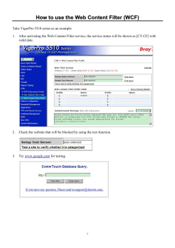


© Copyright 2026