
TRANSPARENT ELECTRODES FOR OPTOELECTRONIC DEVICES BASED IN ZnO AND GRAPHENE
TRANSPARENT ELECTRODES FOR OPTOELECTRONIC DEVICES BASED IN ZnO AND GRAPHENE OXIDE XAVIER DÍEZ BETRIU TRANSPARENT ELECTRODES FOR OPTOELECTRONIC DEVICES BASED IN ZnO AND GRAPHENE OXIDE (Electrodos transparentes para dispositivos optoelectrónicos basados en ZnO y óxido de grafeno) Memoria presentada por Xavier Díez Betriu Para optar al grado de Doctor en Física por la Universidad Autónoma de Madrid Directora de Tesis: Prof. Alicia de Andrés Miguel Tutora: Prof. Luisa E. Bausá Madrid, octubre de 2014 AGRADECIMIENTOS Este trabajo ha sido posible gracias al apoyo y la ayuda, tanto a nivel científico como personal, de la gente que ha estado a mi alrededor durante este tiempo. Es por ello que quería agradecerles a todos ellos el haber estado ahí. En primer lugar quería agradecer a mi directora de tesis, Alicia de Andrés, la dedicación, tesón y paciencia que ha tenido durante todo este tiempo para que saliera adelante el trabajo así como su buena predisposición a la hora de ayudar en las medidas ópticas y enseñarme Raman y difracción. A Carlos Prieto por la paciencia y la ayuda a la hora de enseñarme a utilizar los equipos de sputtering. También agradecer a Rafa y Federico por los momentos que pacientemente han dedicado a explicar los entresijos del Brillouin y la difracción. A mi tutora de tesis, la profesora Luisa Bausá por su atención y buena disponibilidad. A Carmen Munuera por su colaboración y ayuda en las medidas de AFM. Agradecer a Mar, Norbert, Rafa y Luis el compañerismo estos años tanto en el instituto como cuando hemos coincidido en congresos. A Susana por su inestimable ayuda y paciencia con las medidas de Raman así como las charlas en el despacho. A Jorge Sánchez por su compañerismo e inagotable disponibilidad a resolver preguntas estúpidas. A los compañeros del grupo que están o han pasado durante estos años y con los cuales hemos compartido muchos momentos: Esteban, Félix, Leo, Ana, Eva, Eduardo, Mº Ángeles, Aurora y Rocío. A los miembros del grupo de Optoelectrónica Orgánica de la Universidad Rey Juan Carlos, Carmen Coya, Ángel Luis Álvarez y Miguel García-Vélez, por acercarme al mundo de la fabricación de los dispositivos optoelectrónicos. Al Dr. Vincenzo Palermo e a tutto il gruppo di Nanochimica del ISOF di Bologna (Andrea, Kostas,…) per accogliermi nel gruppo e avere reso il mio soggiorno un’esperienza magnifica. Al grupo de los fotónicos con los que tanto hemos discutido: Juan, Cefe, Álvaro, Miguel, André, Luzca… También a los compañeros de despacho que he tenido durante este tiempo: Loreto, Jon, Antonio y el tete Alberto. A la gente del ICMM con la que he compartido muchas charlas de pasillo, comedor y fiestas de Navidad como Marisa, Constanza, Chicho, Sandra, Anto,… Als meus pares i a la meva germana, els quals sempre m’han donat suport i m’han ajudat en tot el que ha calgut. A la Carmen i a l’Antonio, que sempre m’han tractat com a un Cruceyra més i m’han ajudat i acollit a casa seva incondicionalment. Sense ells, l’experiència de viure a Madrid no hagués estat el mateix. A la Montserrat, l’Albert, el Xavier i l’Eduard que malgrat els temps difícils que han estat aquests darrers anys hem pogut compartir bons moments. Als amics que m’han acompanyat durant aquests anys a Madrid (Maria, Alba, Marc, Thom,…) especialment als malaguitas (Paloma, Virginia, Emilio…), al David Flagio per la rebuda a la ciutat i a l’Àngel Fernández pels grans concerts i les infinites vetllades a casa seva. To Lindy, for all the good moments we had and the good ones to come. Als meus pares i a la meva germana, “Il 'senso comune' è il folklore della filosofia e sta di mezzo tra il folclore vero e la filosofia, la scienza, l'economia degli scienziati.” Antonio Gramsci “There is no patent. Could you patent the sun?” Jonas Salk TRANSPARENT ELECTRODES FOR OPTOELECTRONIC DEVICES BASED IN ZnO AND GRAPHENE OXIDE RESUMEN EN CASTELLANO……………………………………………………....1 1.INTRODUCTION - Transparent Conducting Materials................................................................7 -Graphene as a candidate material for optoelectronic devices.........................8 - Electronic structure.............................................................................10 - Graphene Properties and Obtention...................................................12 - Applications.........................................................................................14 - A new family of graphene materials by means of graphite exfoliation.......16 - Graphite Oxide and Graphene Oxide synthesis..................................17 - GO structure........................................................................................18 - Hydrophilic character and metastability............................................21 - Tailored synthesis................................................................................22 - Reduction of GO: Recovering the lattice.......................................................23 - Evaluation of reduction degree...........................................................24 - Reduction Methods..............................................................................26 - Selectivity of the chemical reagent......................................................28 - Restoring the lattice.............................................................................29 - Alternative strategies: Hybrid Materials............................................32 - Raman Spectroscopy of Graphene................................................................33 - Disorder in graphene..........................................................................36 - Oxidation and disorder.......................................................................39 2.THIN FILMS GROWTH AND CHARACTERIZATION TECHNIQUES -Thin Films growth techniques........................................................................45 - Sputtering deposition...........................................................................45 - Spin coating.........................................................................................47 -Characterization techniques...........................................................................49 - Structural Techniques..........................................................................49 - X-Ray techniques....................................................................49 - X-Ray Reflectivity.......................................................49 - X-Ray Diffraction (XRD)...........................................51 - Experimental set up for synchrotron X-ray diffraction.....................................................................53 - Chemical Analysis Techniques............................................................55 - X-Ray Photoelectron Spectroscopy (XPS)..............................55 -Optical Techniques...............................................................................56 -Raman Spectroscopy................................................................57 -UV-VIS Transmission Spectroscopy........................................59 -Spectroscopic Ellipsometry......................................................59 -Morphological Techniques...................................................................60 - Atomic Forces Microscopy.....................................................61 - Transport Properties...........................................................................63 - Electrical Measurements..........................................................64 3. AMORPHOUS Al-DOPED ZnO INORGANIC TRANSPARENT ELECTRODES FOR FLEXIBLE DEVICES - Target preparation..........................................................................................70 - Thin films growth...........................................................................................71 - Thickness determination................................................................................73 - Crystallinity analysis......................................................................................75 - Optical band gap............................................................................................79 - Conductivity....................................................................................................81 - Conclusions....................................................................................................82 4. FEW LAYER REDUCED GRAPHENE OXIDE THIN FILMS - Parent graphites.........................................................................................88 - GO synthesis and exfoliation.....................................................................89 - Powder thermal reduction..........................................................................94 - Thin films preparation................................................................................94 - Substrate surface........................................................................................95 - Thickness calibration.................................................................................96 - Reduction of GO thin films........................................................................97 - Patterning..................................................................................................101 - Conclusions...............................................................................................103 5. REDUCTION AND RESTORATION OF THE CARBON NETWORK: ON THE WAY BACK TO GRAPHENE - The Starting Point: Graphene Oxide...........................................................109 - Peak fitting........................................................................................109 - Raman spectra of graphene oxide....................................................110 - Quantifying the order........................................................................113 - Graphene Oxide reduction process.............................................................114 - Strain simulations.............................................................................118 - Thermal reduction.............................................................................120 - Deoxygenation mechanism in thermal reduction..............................121 - The role of water...............................................................................122 - New carbon bonds and ordering.......................................................123 -Optimization of the reduction process................................................127 - Transport properties vs reduction................................................................130 - Conclusions..................................................................................................132 6. IMPACT OF THERMAL AND CHEMICAL REDUCTION ON FEW LAYER GRAPHENE STACKING - Samples preparation.....................................................................................139 - X-Ray set up.................................................................................................139 - Stacking of Graphene oxide in thin films...................................................140 - Thickness influence on stacking..................................................................141 - Thermal annealing.......................................................................................143 - Stacking simulations....................................................................................147 - Roughness and Flakes folding....................................................................152 - Stacking and conductivity............................................................................156 - Conclusions..................................................................................................157 7. HYBRID rGO – Au THIN FILMS FOR TRANSPARENT ELECTRODES - Hybridization strategies................................................................................164 - Au Nanoparticles growth.............................................................................164 - Chemically reduced hybrid films.................................................................166 - Thermally reduced hybrid films...................................................................169 - Conclusions & Outlook................................................................................173 8. ON THE FRAGMENTATION PROCESS OF THE GRAPHENE OXIDE - Fragmentation by means of ultrasounds.....................................................178 - Image processing..........................................................................................179 - Fragmentation analysis................................................................................181 - Conclusions & Outlook................................................................................187 9. CONCLUSIONES..................................................................................................191 LISTA DE PUBLICACIONES..................................................................................196 RESUMEN El objetivo general de esta tesis es el desarrollo de nuevos electrodos transparentes para dispositivos optoelectrónicos. Los materiales aptos para su aplicación como electrodos transparentes deben presentar una alta transparencia en el espectro del visible y una alta conductividad. Recientemente con la aparición de la llamada electrónica flexible, también son requeridas propiedades mecánicas específicas. En las últimas décadas, las nuevas aplicaciones tales como dispositivos para emisión de luz, energía fotovoltaica o pantallas táctiles, por ejemplo, han exigido un gran esfuerzo en el desarrollo de los electrodos transparentes. El mercado está actualmente dominado por el ITO (In-Sn-O) y hay una gran actividad en la búsqueda de distintas alternativas. Los materiales conductores transparentes más estudiados son los llamados Óxidos Transparentes Conductores (TCO en sus siglas en inglés) basados en óxidos metálicos, principalmente de Sn, In, Zn y Cd, los cuales se pueden dopar o combinar para mejorar sus propiedades conductoras. El reto más reciente es la obtención de estos electrodos con las propiedades mecánicas adecuadas para su implementación en los dispositivos en electrónica flexible y en electrónica de gran área. Por tanto un objetivo primordial es obtener electrodos amorfos o nano-particulados manteniendo las propiedades ópticas y de transporte y, además, empleando temperaturas de síntesis o de depósito y de procesado suficientemente bajas para su compatibilidad con substratos flexibles. La irrupción del grafeno ha supuesto una apertura de posibilidades de desarrollo en el campo de la ciencia y tecnología de materiales. Específicamente, el campo de los electrodos transparentes, el grafeno supone el candidato ideal ya que su alta transmisión en el rango desde el UV hasta el MIR y la altísima movilidad de los portadores ofrecen la posibilidad de una mejora respecto al TCO por excelencia, el óxido de indio dopado con titanio (ITO). El principal obstáculo a vencer para la implementación del grafeno como electrodo transparente es la obtención a gran escala de grafeno de alta calidad. Para conseguir este objetivo existen diversas estrategias de síntesis. La exfoliación del 1 grafito mediante oxidación y la posterior reducción del óxido de grafeno obtenido es un método extendido que aporta una gran facilidad de procesado y de implementación en dispositivos y, además, es escalable a nivel industrial. A pesar de ello, el proceso de reducción no es completo e implica la formación de defectos que lastran las propiedades originales del grafeno. En términos de investigación se está realizando un gran esfuerzo para minimizar los efectos del proceso oxidación-reducción y conseguir las propiedades de conducción y transparencia óptimas para su aplicación como electrodo transparente. Este trabajo se ha centrado por un lado en obtención de electrodos transparentes amorfos basados en óxido de zinc dopado con Al compatibles con la electrónica flexible y, por el otro, en el estudio y desarrollo de películas ultra-delgadas conductoras y transparentes basadas en óxido de grafeno. En este caso se empleó la vía química es decir partiendo de suspensiones de óxido de grafeno provenientes de la oxidación y exfoliación de grafito. Se obtuvieron las condiciones óptimas para la formación de películas continuas y homogéneas de pocas monocapas (2-10) y para su reducción. Se han estudiado y comparado los mecanismos de reducción química y térmica y se ha puesto de relieve la importancia del apilamiento de las monocapas de óxido de grafeno de las películas en sus propiedades. Desde el punto de vista tecnológico, se ha participado en la evaluación de las posibilidades de aplicación de una técnica de litografía que permite realizar motivos a escala micrométrica en un solo paso a las películas obtenidas, tanto de ZnO:Al como las basadas en óxido de grafeno. Se emplearon técnicas físicas de depósito, en particular “sputtering” asistido por magnetrón, para las películas de óxidos y metales mientras que para las películas de materiales relacionados con el grafeno se empleó la técnica de “spin coating” a partir de suspensiones. Se optimizaron los parámetros específicos de cada técnica de depósito para la obtención de los distintos materiales. Se emplearon diversas técnicas para la caracterización estructural y morfológica: difracción y reflectividad de rayos X, microscopía de fuerzas atómicas, microscopía óptica y elipsometría. La caracterización óptica, química y electrónica se realizó empleando espectroscopía Raman, de transmisión óptica y de rayos X (XPS). Para las medidas de conductividad eléctrica se puso a punto un sistema de micro-posicionadores que permite realizar medidas en contactos y áreas de decenas de micras. 2 Electrodos transparentes inorgánicos para substratos flexibles La irrupción en el mundo de la tecnología de la llamada electrónica flexible supone un reto a la hora de adaptar y optimizar las propiedades mecánicas de los materiales que forman los dispositivos flexibles. Por esto motivo en este capítulo se presenta un estudio de las propiedades ópticas y electrónicas del óxido de zinc dopado con Al en función de la cristalinidad. También se han estudiado las condiciones de crecimiento del material ya que su aplicación en dispositivos con materiales orgánicos exige un procesado compatible con su naturaleza. De este modo, se han tenido en cuenta unas condiciones de crecimiento a temperatura ambiente y un tratamiento térmico a temperaturas compatibles con los principales substratos orgánicos. Obtención de láminas delgadas de óxido de grafeno reducido La obtención de láminas delgadas de óxido de grafeno reducido se ha hecho a partir de tres distintos óxidos de grafeno proporcionados por el INCAR (Instituto Nacional del Carbón – CSIC) de Oviedo. El control de los tres grafitos de partida (dos sintéticos y uno comercial) permite obtener tres óxidos de grafeno con distintas proporciones de grupos funcionales de O y con distintos tamaños de lámina. El depósito de las láminas de óxido de grafeno se ha llevado a cabo a través de la técnica llamada spin coating. Se han determinado las condiciones de depósito sobre distintos substratos como Si, vidrio y sílice fundida. El grosor de dichas películas se ha obtenido mediante la calibración con un microscopio de fuerzas atómicas (AFM) de la intensidad del pico G del espectro Raman del óxido de grafeno. La reducción química de las películas se ha hecho utilizando hidracina como agente reductor. Se han optimizado los parámetros y se ha monitorizado el grado de reducción a través de espectroscopía Raman. La colaboración con el laboratorio de caracterización de dispositivos orgánicos de la universidad Rey Juan Carlos ha permitido determinar las condiciones de grabado de patrones mediante descarga eléctrica sobre películas tanto de óxido de grafeno como de su versión reducida para su posterior uso en dispositivos. 3 Reducción y restauración de la red de carbono El estudio detallado de la reducción y restauración del grafeno a partir del óxido de grafeno se ha llevado a cabo a partir de diversas técnicas de caracterización y principalmente a través de la espectroscopía Raman. El estudio de los defectos de los óxidos de grafeno de partida ha permitido distinguir tres modos Raman de baja intensidad que pueden ser asociados a modos de estiramiento de los enlaces C-H y a anillos irregulares. Estos modos desaparecen para muestras de alto orden estructural. Gracias a la optimización de la reducción, se han conseguido láminas de grafeno derivado químicamente con un alto orden en la red de carbono. Se ha observado la reducción y la restauración de dicha estructura. El grado de reducción y de restauración depende del óxido de partida. Se han estudiado también la relación entre la reducción de y las propiedades de transporte de las láminas de grafeno derivado químicamente. Mediante la combinación del tratamiento químico y térmico se ha logrado mejorar la conductividad en las zonas de solapamiento entre monocapas. Impacto de la reducción química y térmica en el apilamiento del óxido de grafeno La mejora de la conductividad en la zona de solapamiento entre las monocapas de óxido de grafeno reducido ha llevado a estudiar el apilamiento de las capas al depositarse sobre el substrato, qué influencia tiene sobre las propiedades y cómo afecta el proceso de reducción, ya sea químico o térmico. Para ello se han depositado las capas sobre Si y vidrio las cuales han sido posteriormente reducidas por vía química o térmica y se han sometido a experimentos de difracción de rayos X en las instalaciones del sincrotrón ESRF. El estudio de difracción se ha complementado con el uso de AFM el cual ha permitido determinar las distancias óxido de grafeno-substrato y las características morfológicas de copos individuales de óxido de grafeno en distintas condiciones. 4 Materiales híbridos basados en películas ultra-delgadas de Au y monocapas de GO para aplicación en electrodos transparentes La síntesis y procesado de películas de grafeno genera una serie de defectos en su estructura que merman sus propiedades originales. La combinación del grafeno con otros materiales es una estrategia emergente no sólo para reparar de forma selectiva los defectos y recuperar las propiedades deseadas del grafeno sino que puede añadir nuevas funcionalidades. Para ello se ha estudiado la formación y las propiedades de láminas ultra-delgadas de Au para su posterior combinación con películas de GO y rGO (tanto reducido térmicamente como químicamente). Fragmentación Con el objetivo de proporcionar herramientas para el conocimiento y la producción de monocapas óxido de grafeno, se ha realizado un estudio estadístico sobre su fragmentación al aplicar ultrasonidos. Por este motivo se han preparado las suspensiones acuosas correspondientes y las monocapas fragmentadas de óxido de grafeno se han depositado de modo que las monocapas no estuvieran en contacto. El tratamiento digital de las imágenes y la aplicación de un software específico (SPIP) para el análisis de cuantitativo ha supuesto gran parte de este trabajo. Las principales variables a estudiar fueron la longitud, el tamaño y el ancho de cada monocapa (o partícula). Las muestras se estudiaron a través de diversas técnicas de microscopía tales como microscopía óptica, microscopía de fluorescencia, microscopía electrónica de barrido (SEM) o microscopía de fuerzas atómicas (AFM). Las conclusiones de los estudios que aquí se indican vienen resumidas en el capítulo final de esta memoria. 5 6 CHAPTER 1 INTRODUCTION Transparent Conducting Materials During the last decade there has been a huge increase of interest in materials displaying at least two simultaneous properties: conductivity and transparency in the visible range. The reasons for such an investment of time and resources to study and develop this materials family is strongly linked to the technological development. Several technological branches coincide when pushing the research on developing competitive transparent conducting materials. These applications are mainly formed by solar cells, portable electronics, displays, flexible electronics or thin film transistors. Being the application range that wide, the nature of the materials integrated in these applications is consequently broad including metals, ceramics, organic polymers… Thus, the requirements for transparent conducting materials are not only based on better performance properties but also in terms of suitable processability and even morphology. Historically, transparent conducting materials have been mainly dominated by what is called Transparent Conducting Oxides (TCO). This family of materials is formed by crystalline compounds based on metallic oxides mainly of In, Sn, Zn and Cd which usually are doped to increase the conductivity. The main oxides compositions and their doping are listed in the table below. 7 Table 2. TCO for thin film transparent electrodes. Adapted from reference 1. However, the research has pushed to expand the range to other metals and even with binary and ternary oxides. Despite the inorganic presence of the transparent conducting materials, the irruption of organic light-emitting diodes (OLED), organic photovoltaic devices (OPV) and flexible electronics has opened the scope to other materials. The focus has been on conducting polymers 2, charge transfer polymers like PEDOT:PSS 3, carbon nanotube composites 4 and graphene. The conductive performance of these materials is lower than the best TCO but offers a huge potential to implement into organic/flexible devices at room Graphene as a candidate material for optoelectronic devices The 2010 Nobel prize award in Physics was for two russian physicists (A. Geim and K. Novoselov) who work in the Manchester University. The reason for such recognition was the discovering of a material called graphene. Actually, this material 8 was not exactly new (because previously studied by theoreticians 5) but they were able to obtain it for the first time and study it experimentally 6. The importance of graphene relies on a broad range of features (conductor, transparent, flexible, inert, mechanically resistant…) that makes it the wonder material that would be able to change the current technology. After its first obtention, the race for graphene technology development started. One of the main advantages of graphene is the availability of its source. Graphene is a carbon material that can be prepared directly from graphite, which is easily synthesizable, or from a carbon source like methane. Graphene is made entirely of carbon atoms so it is considered an allotropic form of C. Some elements in solid state can be structured in different forms while keeping the chemical composition. Every one of these structures is an allotrope and for the carbon case, there are several, natural or synthetic, allotropes as depicted in figure 1. Diamond (figure 1a) is one of the most known allotropes for all the publics. Also, graphite (figure 1b) is a material with a large and old use in human history. Newer allotropes (figure d and c) have been isolated recently like fullerenes 7 or nanotubes 8. a) b) c) d) Figure 1.Structure of the main allotropic forms of carbon a) Diamond b) Graphite c) Nanotube d) Fullerene. 9 The reason for these materials to hold the same chemical composition and a different structure is found in the bonding between the atoms. Tetrahedral geometry is obtained for C-diamond atoms or trigonal planar for C-graphite atoms. The resulting behavior and properties from both materials are radically different. While tetrahedral geometry in diamond gives place to a 3D crystal, trigonal planar geometry results in a planar disposition of the carbon atoms. Every one of these sheets made of carbon is what is called graphene. However, it is not found isolated in nature but stacked up in a huge number of sheets commonly known as graphite. Electronic Structure The main characteristic of graphene relies in its singular electronic structure. The hexagonal atomic disposition gives place to a two carbon triangular sublattices (figure 2a) with the high-symmetry points in the first Brillouin zone labeled M, K, K’ and Γ. Each carbon atom has one s and three p orbitals. The s and the two in-plane p orbitals are linked together to form the covalent bonding by means of sp2 hybridization. As a result, the hybrid orbitals σ and σ* are formed and they do not contribute to conductivity. The remaining p orbital is out-of-plane and forms a π valence band and a π* conduction band. a) Γ M Brillouin zone b) σ π Figure 2. a) Scheme of graphene’s crystal structure where the Brillouin zone is highlighted indicating the symmetry points. From reference 9. b) σ and π bands along the Brillouin zone. Extracted from reference 10. 10 In the Bloch band description of graphene’s electronic structure, orbital energies depend on the momentum of charge carriers in the Brillouin zone. The π and the π * bands (figure 2b) are decoupled from the σ and σ* bands because of inversion symmetry. Since they have a smaller contribution in bonding, the π and π* energies are closer to the Fermi level where occupied and empty states are separated. In a neutral graphene sheet, this is the energy where valence and conduction bands meet around K and K’ high-symmetry points in the Brillouin zone forming conical valleys. The points where both bands meet in K or K’ are known as Dirac points. Because the bands have zero energy at these points, they are also often referred to as neutrality points. Near these points the energy varies linearly with the magnitude of momentum measured from the Brillouin-zone corners. The four other Brillouin-zone corners are related to K and K’ by reciprocal lattice and do not represent distinct electronic states. Figure 3. Schematic energy relation dispersion in the around the Dirac point (K) in the Brillouin zone. a) represents the neutral state of graphene’s energy dispersion relation when Fermi level and neutrality point coincides. b) The Fermi level has lower energy and electrons are partially drained from the valence band resulting in a hole-doping. c) The Fermi level is pushed towards higher energy values so they are electrons in the conduction band (negatively-doped). Extracted from reference 11 Graphene transport properties are very sensitive to the interaction with the substrate, to chemical doping or to the application of an external electric field that separates the Fermi level from the Dirac point. This phenomenon allows playing with electronic properties of graphene with external agents as schematically depicted in figure 3. For example, when graphene is in contact with an electron donor material, the 11 Fermi level is pushed towards the conduction band in such a way that graphene is electron doped. The same happens for the opposite case: when graphene is in contact with an electron withdrawing material, electrons are drained from the valence band and thus, gets positively doped. Also, there is the possibility to apply a gate potential in the substrate material (where the graphene is supported) to apply a positively or negatively doping. Graphene Properties and Obtention The first time graphene was isolated was thanks to the mechanical exfoliation of graphite 6. Actually, this technique is a cheap and easy way to obtain high quality samples by means of direct exfoliation of graphite with a scotch tape yielding graphene flakes of high quality. Unfortunately, these graphene flakes cannot be transferred to devices or used for practical applications. However, many graphene features have been measured with mechanically exfoliated samples showing a unique behavior: roomtemperature electron mobility of 2.53·105 cm2V-1 s-1 and intrinsic strength of 130 GPa 3,000WmK-1 14 13 ; very 12 , a Young’s modulus of 1 TPa high thermal conductivity (above ); optical absorption of πα<2.3% (in the infrared limit, where α is the fine structure constant)15; complete impermeability to any gases 16 , ability to sustain extremely high densities of electric current (106 times higher than copper) 17 . Another important property is the possibility of graphene’s chemical functionalization opening a wide range of extra functionalities and applications. Nevertheless, all these properties have been obtained with a non-scalable technique like the mechanical exfoliation of graphite and the observed properties for high-quality graphene have not being obtained yet for other production pathways. Unfortunately, there is not yet a mass production method of graphene for a direct transfer into real technology. Although the methods for industrial production are improving, there is a big effort and investment on reach graphene’s mass production with the quality standards to exploit graphene’s properties. The methods for graphene obtention can be regarded with the classical top-down and bottom-up approaches. The bottom-up processes involve the growth of graphene layers over several kinds of substrates. Chemical Vapor Deposition (CVD) is an 12 extended method to grow large-area graphene films by means of organic gases on metal substrates like Ni 18, Ru19 or Cu20. Figure 4. Scheme of the CVD mechanism extracted from reference21 In the CVD technique, methane and hydrogen (among other examples of reactant gases for this reaction) are used as reactants (figure 4). Both gases are driven into a furnace where there is a copper foil and the reaction takes place at high temperatures (≈ 900 – 1000 ºC). The metallic substrate acts as a catalyst for methane decomposition and as an effective support for graphene crystals growth. They are also modified set ups based on the vapor reaction like the Plasma Enhanced-CVD CVD). 22 (PE- Other bottom-up methods are having been developed like the direct graphitization over Si-C 23 with high-temperature annealing and wet chemical reaction by organic synthesis24. On the opposite side there is the top-down approach where the graphite is used as a starting point to scale-down the material and achieve the few- or single-layer graphene. The main advantages of these approaches are the high yield, the solutionbased processability and the ease of implementation. Exfoliation of the parent graphite is the goal to obtain single sheets and can be achieved by different ways. Liquid-phase exfoliation is based in the use of a solvent to take advantage of its ability to adsorb and accommodate in the graphite structure to subsequently split the graphene sheets by means of ultrasounds 25. 13 Exfoliation can also be achieved by means of chemical oxidation of the parent graphite with sonication assistance26. When oxidizing graphite, O atoms are introduced in the carbon lattice occupying the intersheet space. Also, the bonding between C and O forces the sheet to wrinkle resulting in a weakening of the Van der Waals forces of sheets stacking. The use of ultrasounds gives the energy to breaking the stacking forces and to exfoliate the sheets. Once exfoliated, the graphene oxide (GO) is stable in aqueous suspension and can be deposited as a thin film over almost any surface and partially reduced to recover the original graphene properties 27 . The chemical functionalization opens also a wide range of applications and uses that will be exposed later. Worth to mention that thermal annealings of graphite oxide may induce exfoliation of graphene sheets 28. Applications Transparent and conductive materials are needed for coatings which are widely used in electronic products such as touch screen displays, e-paper (electronic paper) or organic light-emitting diodes (OLEDs) and require a low sheet resistance with high transmittance (of over 90%) depending on the specific application. Flexible electronics is a technology where electronic circuits are assembled on flexible substrates. The advantage of such flexible technology is the ability to give new functionality to the existing electronics technology. Graphene meets the electrical and optical requirements with an excellent transmittance of 97.7% for a single layer 8, although the traditionally used indium tin oxide (ITO) still demonstrates slightly better characteristics. However, the affordability, price and limited mechanic flexibility of ITO gives graphene in a good position for succeeding when its quality improves. In the field of organic electronics (which may include the flexible electronics), OLED’s are devices already in the daily technology. Graphene’s work function tunability is expected to improve the efficiency and its atomically flat surface would help avoid electrical shortcuts and leakage currents. In the field of electronic devices, graphene is being widely studied for direct application in high-frequency transistors 29 and logic transistors30. 14 Energy technologies are also expected to have benefits from graphene’s application. Research is based on solar cells development where graphene can contribute as an active layer or, alternatively, can be used as a transparent material electrode 31 . Energy storage is another big place for graphene implementation and specifically as part of the cathode for next-generation lithium-ion batteries. Graphene, with its sheet-like morphology, would be able not only act as an advanced conductive filler but may also give rise to novel core–shell or sandwich-type nanocomposite structures32. Electrical double layer capacitors (EDLC) are based on the high capacitance generated by electrostatic charge accumulation at the electrode/electrolyte interface that is usually proportional to the effective surface specific area (SSA) of the electrode material. Big efforts are done in order to achieve graphene-based highperformance supercapcitors 33 since graphene appears as an ideal candidate because of its high SSA, low resistance and thermal and mechanical stability. Moreover, graphene shows a wavelength-independent absorption for normal incident light below about 3eV that can be exploited for photonic applications. Specifically, this property can be used for a wide spectral range (from infrared to ultraviolet) to photo-generate small interband transitions and thus work as a photodetector 34. Thanks to the application of an external drive voltage, this graphene’s optical response can be varied giving rise to act as an optical modulator 35. An important field for graphene’s industrial development is the composite materials area. The mechanical, chemical, electronic and barrier properties of graphene along with its high aspect ratio make graphene attractive for applications in composite materials. The use of graphene-based paints can be used for conductive ink, antistatic, electromagnetic-interference shielding, gas-barrier and corrosion-barrier applications. The obtention method and their corresponding properties and applications are summarized in table 3: 15 Table 3. Graphene obtention methods, its properties and applications adapted from reference36. A new family of graphene materials by means of graphite exfoliation The top-down approximation to graphene obtention gives several options for exfoliated graphene and derivatives yielding. Among them, graphite oxidation is an easy way to produce a water processable graphene derivative that opens a wide range of uses. The oxidation of the parent graphite allows the exfoliation of the graphitic sheets but also introduces O groups into the C lattice. The chemical functionalization introduces new chemical groups by breaking the original sp2 hybridization of the network. Therefore, the π-π band is broken modifying completely the electronic structure and its original properties. Graphene oxide becomes useless for conductive applications since it is an insulator. Once oxidized, graphene is easier to be chemically functionalized and new opportunities are open to bioapplications like drug delivery 37 . Its mechanical applications may allow tissue engineering and regenerative medicine 38 . Also, chemically functionalized graphene might lead to fast and ultrasensitive 16 measurement devices, capable of detecting a range of biological molecules including glucose, cholesterol, hemoglobin and DNA 39. Nevertheless, these extended functionalities are a serious inconvenient when trying to use graphene oxide for conductive purposes. graphene oxide (rGO) by many ways 40 The ability to reduce the is getting beyond the oxidation-reduction setbacks and making an excellent approach for mass scale production and optoelectronic devices as shown in their use as transparent conductors 41, sensors 42, thin films transistors (TFT)43 , electrodes 44 or photovoltaics 45. The advantages of an aqueous solution based process and the large specific surface area (SSA) yield an excellent material for batteries and energy storage technology 46 . For this specific field, rapid thermal exfoliation is a good synthesis method because of the high porosities obtained 9. Graphite Oxide and Graphene Oxide synthesis Although the interest in graphene synthesis and application is very recent graphite and its derivatives are known since almost two centuries ago 48 47 , . In the search for the molecular formula for graphite, De Brodie was the first to treat this compound with heavy oxidizing agents like fuming HNO3 and HClO3. The result of this oxidation was partially exfoliated graphite with oxygen incorporated into its structure. A few decades later, researchers like Staudenmaier 49 , Hummers and Offeman 50 worked in alternative ways for graphite oxidation. Since then, there have been slight variations of the primary method although the basis of oxidation remains. However, the product of the reactions was found to be different depending not only on the chemical actors but also in other factors like parent graphite51 and the reaction conditions 52. However, these methods for oxidizing graphite yield flakes containing few graphitic layers stacked together by the original Van der Waals forces and they are called graphite oxide. The interlayer space is highly hydrophilic and allows embedded water 53 . To achieve the complete exfoliation of the graphite oxides flakes into graphene oxide monolayers it is necessary to further exfoliate the materials by means of sonication 54 . To visualize the difference, both oxides are schematically depicted in figure 5. 17 a) Graphite Oxide b) Graphene Oxide Figure 5. Schematic representation of graphite oxide (a) and graphene oxide (b). While in the first structure the layers remain stacked as a unit, the graphene oxide layers remain independent one to another. The complexity of the obtention of either graphite oxide or graphene oxide can make the resulting compounds very different depending on the method. This fact turns into an advantage due to the wide range of application for this materials family. Notwithstanding, this variability in the resulting oxide opened the way to study and understand the graphite oxide formation mechanism, structure and then, the way to tailor its characteristics. GO structure For its further development it is crucial to know and understand its composition and structure. Such an achievement has not been clearly defined with precision and an intense debate is still open. From the initial model proposed by Hoffman and Holst 55 (figure 6a) where a graphitic structure including 1,2 – epoxides was presented, other models and variations have been proposed 56,57,58 . In the last ten years several studies helped to confirm and elucidate some questions although other structural issues that remain unsolved. 18 a) b) c) d) e) f) Figure 6. Schematic structures for the main models for graphite oxide. a) Hoffman model with 1,2-epoxy groups. b) Ruess model with sp3 basal planes and 1,3-epoxy groups. c) Scholz-Boehm model incorporating hydroxyl and ketone groups. d) Nakajima-Matsuo model similar to a graphite intercalation compound. e) LerfKlinkowski model with hydroxyl and epoxy groups in the basal plane with three different regions:holes, graphitic regions and disordered regions. f) Szabö-Dékany model including corrugation and close epoxy and hydroxyl groups in the basal plane. Extracted from reference 59. The TEM study of Erickson and coworkers of direct observation of a single layer of graphene oxide proved the coexistence of pristine graphitic regions, holes and areas with a high presence of O-related defects 60 . Here, the model of Lerf and Klinowski (L-K) 61 (figure 6e) is partially confirmed because proves the existence of the graphitic domains with areas of disordered carbon but does not give clear information of the O-functionalized areas. Lerf and Klinowski, by means of nuclear resonance techniques, suggested that these areas were mainly functionalized with hydroxil and 1,2-epoxy groups in the basal plane whereas the edges were populated with carboxyl and hydroxyl groups. The O-groups at the basal plane in the L-K model were also meant to be very close. A few years after, the nucleation and formation of concentrated 19 O-groups was predicted 62 and Cai et al 63 confirmed by means of Solid State Nuclear Magnetic Resonance (SSNMR) the close relation between the epoxide and the hydroxyl groups in the basal plane. That observation also corroborated the Szabö and Dékany model 64 (figure 6f) where the oxidation of the sp2 network is taken as a network of linked cyclohexanes. This structural model seems to fit better in the overall experimental observations and also includes the corrugation of the flakes. Although the major features of the structure have been discovered, minority functional groups have been observed by means of RMN as showed in figure 7. Figure 7. GO structure model that incorporates the latest functionalities observed on the periphery of the flakes. Extracted from reference 65. New groups such ketones, ester or lactols are present in small proportion on the edges of the carbon rings. Therefore, a detailed description of the functional groups on the periphery of the graphite oxide is still being needed 65. a) b) Figure 8. Aberration-corrected TEM image of a GO (a) where colors are used in (b) to indicate the main structural features: green for ordered graphene structure with hydroxyl/epoxy groups, blue for ordered graphene structure, yellow for amorphous graphene and red for holes. Adapted from reference 66 20 In figure 8, the structure of a GO by means of transmission electronic microscopy is showed. Clearly, it is possible to see how graphitic domains are maintained and the disordered green areas are functionalized with epoxy and hydroxyl groups. It worth to point out the presence of holes and highly disordered structures in their vicinity. Hydrophilic character and metastability The stacking of graphite oxide layers have been studied 68 67 as well as its stability . The high hydrophilic behavior of graphite oxide allows a considerable amount of embedded water in the interlayer space 13 that plays an active role in the bonding between planes 69 thanks to the H–bond interactions (figure 9). Figure 9. Scheme of the proposed model for water bonding to the graphite oxide structure. Extracted from reference 74. Despite the knowledge about graphite oxide, only an incipient work has been done in graphene oxide stacking. First detailed studies in graphene oxide introduced the idea of the inner corrugation 70 and the adsorbed water 71 as important factors in stacking as well as its properties. Recent works followed this idea regarding the 21 importance of the flakes arrangement in the electronic properties 72 but not deep experimental studies are done yet. In spite of the difficulty to get the exact picture of the graphene oxide structure and arrangement, there is another variable that adds more complexity to the material. The reactive nature of the graphene oxide gives a metastable character since its chemical features vary along with time. The instability of some of the functional groups, mainly epoxides, becomes in a spontaneous loss of epoxy groups and the formation of water 73 that remains adsorbed in the surface or in the interlayer for stacked flakes. This process happens at room temperature and the O-content of GO stabilizes between 40 and 70 days. Parallel to this process, there is a spontaneous decomposition in room atmosphere by means of CO2 formation 74 that leads to the formation of holes in the flake structure. Tailored synthesis The knowledge of the main structural features is the key step to an ad hoc oriented synthesis of graphene oxide. Generation of defects is not only related with metastability of graphene or reduction treatments but also with its synthesis and original defects from the parent graphite. The wide range of applications for GO is the result of many chemical and physical variables that can provide GO with different properties. As commented before the range of GO applications is wide and the specific requirements can be absolutely the opposite depending on the role of the material. Energy storage uses for graphene oxide require a high specific surface area. A few general strategies are followed to increase the SSA like rapid thermal exfoliation75, the use of porous structures (like zeolites or foams) or templates 76, 77 . Later, thermal treatments on GO will be discussed but for capacitors applications is important to know how the generation of holes during heating and the ejection of gases yield a spongy GO powder with high SSA values. Table 4 collects the SSA values reached for the different graphene materials obtained by different techniques and is a clear evidence of the large variability of the graphene or graphite oxides. 22 Table 4. Table of methods and SSA adapted from reference 9. When looking for applications in the electronics field, GO with few defects is desirable in order to get a performance as closer as possible to the original graphene. The oxidation of the parent graphite inevitably generates defects and breaks the sp2 hybridization making the material insulating. The exfoliation method is critical determining the defects and holes degree 78 . Also, the parent graphite 51 plays a significant role in the size, morphology and chemical composition of the derivative GO. The need for high electrical conduction and transparency requires preserving as much as possible the original band structure from the C lattice. Larger flakes also help to reduce the resistivity created by the crystal border and flakes overlapping. Large-area synthesis of GO flakes79 and low defects concentration 80,52 have shown good performances and ease of processability. Reduction of graphene oxide: Recovering the lattice For applications looking for high conductivity and transparency, close to the original graphene ones, graphene oxide is not a good candidate. The reversion to the original sp2 C lattice needs to be done in order to recover the original properties. This requires the elimination of the functional groups and in particular the O groups. That 23 process is usually named as reduction of graphene oxide. The full recovery of the original carbon lattice is almost impossible. Nevertheless, research is addressed looking for defects minimization in order to fulfill the specific application requirements. In chemical terms, a complete removal of the O present in the lattice has to be performed. However the complete removal of oxygen does not ensure to obtain the original crystalline structure with the expected properties. All the reduction methods leave behind associated defects for the reduced carbons. The resulting C atom after the elimination of O not necessarily hybridize again with the aromatic bonding of its neighbors and can be incorporated in the lattice as a topological defect. Depending on the method, not only the amount of removed O is important but also the crystalline degree of the lattice should be considered. Therefore, two different stages are taken into account in the original lattice recovery process: the reduction and the restoration. In the first one, the oxygen atoms are removed (deoxygenation) from the lattice without taking into account the mechanism implied. The second stage is intended as a restoration process of the crystal where the entire percent of O (or its majority) is not in the lattice anymore. Also, the defects created are healed resulting in crystallite growth inside the reduced graphene flake. Evaluation of reduction degree Since the goal in this strategy is to get back as much as possible to the original carbon lattice, a parameter for measuring the effectiveness of the process is needed. Furthermore, the complexity added with the two parallel processes makes hard to find a unique magnitude for that purpose. However, they are few indicators of a successful reversion of the oxidation. The first one, and taking into account the chemical meaning of reduction, is the measure of the C/O ratio. By means of X-ray Photoelectron Spectroscopy (XPS) elemental analysis it is possible to determine the relative amount of every element in the compound. Typically the starting graphene oxides have a C/O ratio between 4:1 and 2:1 around 12:1 81 66 . After the reduction, the relation can move towards values of but values as large as 246:1 have been reported 65 . Even, XPS can give more information about the C bonding and hybridization state in the sample (Figure 10). 24 Figure 10. C1s XPS spectra extracted from reference 59 for graphite oxide, dehydrobromination-mediated rGO and hydrazine-mediated reduction. Different kinds of C bonds are shown. Clearly, the C-O related peak suffers a dramatic decrease. The obtained XPS spectra for reduced samples indicate a significant decrease of the presence of oxygen by diminishing the peaks related to the different C-O bonds (Figure 10). On the opposite side, the peak corresponding to C=C bonds, sp2 carbon atoms, increases. The sp2 percent of the overall C is taken as a direct measure of the chemical reduction. In any case, there is always a residual peak related to sp3 hybridized atoms which is usually attributed to C-H (or C-N if hydrazine has been used as a reducing agent) chemical bond. Other techniques like solid-state Nuclear Magnetic Resonance (SS-NMR), Thermo-Gravimetric Analysis (TGA) or Infra-Red spectroscopy are other complementary techniques to give a more detailed picture of the reduction process. Raman spectroscopy is a useful tool for graphene and derivatives analysis because is non-destructive and gives valuable information. The reduction process is usually evaluated using the ratio between the intensity of the D and G Raman peaks using a parallel procedure as that described for the transformation of sp3 carbon to sp2 graphite that will be further discussed extensively. 25 Another magnitude for reduction evaluation, and looking directly to the final result, is the conductivity. Since the reason for reduction is the application in electronic devices where a high conductivity is the desired parameter, the effectiveness of the reduction will be measured in transport properties terms. This magnitude itself does not give a direct measure of the reduction degree but determines the final utility of the material. Table 5. Reduction methods and their corresponding conductivities and C/O ratio. Adapted from reference 82. In table 5, some reduction methods and conductivities are shown. The form in which the reaction takes place and the method implied can yield such different conductivity values. Therefore, they are parameters that have to be taken into account. Reduction methods Reduction of graphene oxide can be faced in many ways depending on the followed strategy. A common and effective method is by thermal annealing performed in an oven and is used both for graphene oxide reduction and for graphite oxide 26 exfoliation and reduction. The rapid temperature increase makes the oxygen-containing functional groups attached on the carbon plane decompose into gases that create a big pressure between the stacked layers. The expansion generated by the CO and CO2 gases produces the exfoliation of the graphitic structure. This double effect (exfoliationdeoxygenation) is a good strategy to produce bulk quantity of graphene. However, the thermal expansion causes a serious damage to the structure resulting in a notable effect in the conductivity properties. Defects inevitably affect the electronic properties of the product by decreasing the ballistic transport path and length and introducing scattering centers. Typically, the conductivity values for the thermal exfoliated graphites are around 10-23 S/cm 82. Worth to say, about 30% of the graphite oxide mass is lost during the exfoliation process 62 leaving behind holes in the graphene sheets. Nevertheless, temperatures higher than 1000ºC produce a restoration effect on the C structure that partially recovers the original aromatic rings and therefore, graphene properties. In the following chapters this subject will be discussed extensively. The treatment with temperature obviously plays an important role in the deoxygenation part because of the different required removal energy for each functional group. The mechanism for oxygen removal will be discussed later. Notwithstanding, other physical ways to perform unconventional heating with good results are microwave irradiation 83 or photo-irradiation 84 . Particularly remarkable, is the easy and efficient way to partially reduce graphene oxide by means of a standard laser optical drive 85,86 . Graphite and graphene oxide reactivity is also used for chemical strategies of reduction. Several chemical agents have been tried being hydrazine hydrate the first and one of the most effectives 54 . The method of GO reduction with hydrazine opened an easy way to mass-production of graphene. Other reducers have also been essayed giving significantly good results like NaBH4 87 . Unfortunately, its reactivity with water (the main solvent for exfoliation and dispersion) makes it not a useful method. Reducing agents with lower toxicity have been proposed with good results. Vitamin C 88 has been showed to be an efficient reductant with a high C/O ratio of 12.5 and conductivity values comparable to those obtained for hydrazine. Also here, worth to mention the use of hydroiodic acid for obtaining reduced GO 89 with significant conductivity (300 S/cm) and C/O ratio (15). Graphene oxide within a wide range of reduction degrees is usually referred as rGO. 27 Selectivity of the chemical reagent Chemical reduction looks for complete removal of O with the advantage of needing much lower temperatures (up to around 100ºC). Up to date, experimental reports have not completely reached this goal although high C/O ratios around 15 have been reported 89 . Chemical reduction is intended to selectively react with specific functional groups. The complexity of the chemical reaction makes difficult to find the exact mechanism but some proposals have been done. The reduction reaction by means of hydrazine was the first to have a suggestion of formal reaction mechanism 54 : Figure 11. De-epoxydation suggested mechanism according reference 54. The reduction mechanism (figure 11) is based in the ring-opening of the epoxide for the formation of hydrazine alcohols, a further formation of aminoaziridine and finally the thermal elimination of the di-imide to restore the double bond. DFT calculations 90 point out the role of hydrazine reducing the epoxy groups and its inability to reduce the hydroxyl, carbonyl and carboxyl groups in GO. According to these calculations, hydroxyl groups attached within an aromatic domain are not stable even at moderate temperatures, and can be removed or migrate to the edges of aromatic domains and restore the conjugated structure after dehydroxylation. Therefore, the reduction mechanism is intended as an epoxy open-ring to form hydroxyl with a further dehydroxylation by moderate heat treatment. The use of other chemical reagents favors the reduction of other functional groups. Sodium borohydride (NaBH4) is another useful reducing agent that selectively may eliminate ketone, lactol, ester and alcohol groups 65. The selectivity of each reducing agent can turn into an advantage when combining them to perform a multi-step strategy. Combination of different methods can bring to more reduced rGO’s. A very interesting approach was realized by Gao et al 65 28 where three steps were used to achieve a very high C/O ratio. First, a two-step reduction stage was performed with NaBH4 for deoxygenation followed by a treatment with H2SO4 for dehydration. Afterwards, a restoration of the graphitic network was performed by means of a thermal treatment at high temperatures (˃1000ºC) under a reducing atmosphere. The result is a highly optimized reduction process for GO with a remarkable conductivity (202 S/cm). Combination of two methods can also help to soften the conditions to obtain the same result. As it was shown by Eda et al 44 , the combination of hydrazine with a soft thermal treatment can achieve the same levels of reduction than a thermal annealing at temperatures around 1100ºC. Restoring the lattice Despite the chemical reduction of graphene oxide, the critical step for rGO application is the recovering of the aromatic lattice to get as closer as possible to the graphene original properties. The chemical reduction can result in an almost O-free material but with many defects that disable its practical application. It is known that chemical reduction can result in doping or residual impurities 91 . Also, thermal annealing results in a highly damaged carbon structure. In spite of the work done trying to explore the thermal mechanism there is not yet a clear explanation although several important factors have been pointed out like the importance of the amount of functional groups in the starting GO and their relative amount and disposition on the carbon sheet. Recent calculations 92 using molecular dynamics simulations of thermally reduced GO at 1500K demonstrate that the relaxation of the lattice around the functional groups when heated at 1500 K produces important deformation of the C network and holes that are very strongly dependent on the initial oxygen content (Figure 12). 29 Figure 12. Calculated GO structures (ref 92) for annealing treatmens depending on the starting O content being a) 25% and b) 33%. Nevertheless, annealing treatments helped with the use of reducing atmospheres 93 or by using reactive gases 94 have been reported in different works to healing the graphitic network. The impact of the temperature treatments on the conductivity of graphene oxide films is complex and both intrinsic and extrinsic components are important. On one hand, for example, Mattevi et al 81 conclude that limitations in conductivity are meant to be directly related with the aromatic (sp2) content of the material. Figure 13 shows how the conductivity increases with the sp2 content. Figure 13. Conductivity values versus the sp2 fraction obtained from reference 81. The vertical line indicates the change of conduction regime. 30 According to these authors, the carrier transport mechanism starts by weak interactions of hopping and tunneling between graphitic regions to achieve a percolation regime where connections between domains are established (figure 14). Figure 14. Structural model at different stages of thermal reduction for a) RT, b) 100ºC, c) 220ºC, d) 500ºC. Growth of graphene clusters and their connectivity are schematically depicted. Extracted from reference 81 . The responsibility for conductivity improvement relies on the elimination of functional groups and its reduction into a new sp2 bonds and/or formation of graphene nanoclusters that open percolation paths. Also, Kobayashi et al 95 studied rGO flakes transport properties concluding that conductivity was governed by the degree of reduction along the C lattice (figure 15a). Figure 15. a) Schematic of RGO nanosheets bridging the source and drain electrodes and the corresponding resistor-network model (bottom) from reference 95 where LS is the major factor contributing to rGO conductivity. b) Sheet resistance as function of transparency (T%at550nm) for flakes of different size in thermal annealed GO (800ºC) extracted from reference 96. 31 On the other side, Su et al 96 compare the conductivity and transparency of films obtained with rGO sheets of different size (figure 15b) evidencing that for the same reduction degree (sp2 content) the conductivity is enhanced when the sheet size is increased. This indicates that hopping from on rGO sheet to another, which is an extrinsic effect, has an important weight in the overall resistance. Therefore not only hybridization degree defines the transport properties, the crystallite (rGO sheets) size, ordering and disposition are significative parameters for conduction. Alternative strategies: Hybrid Materials On the way to achieve the original properties of graphene, there is an alternative option to the healing of defects and the recovering of the lattice. With the combined use of other compounds or materials, the properties of the rGO can be improved significantly. This route, consisting of intercalating layers of rGO with different types of metallic nanoparticles or nanowires, opens up the possibility of fabricating films that could exhibit high transparency, enhanced electrical conductivity, and good flexibility, in addition to enabling attractive biological applications 97. It should be pointed out here the work of Kholmanov et al 98 , who combined the use of Au nanoparticles (NP) and Ag nanowires (NW) (Figure 16). With the right optimization of the hybrid material composition, sheet resistance values of 20-80Ω/sq and transmittances of 80% were achieved being comparables to those of ITO (RS =30 Ω/sq,T550 = 90% ) Figure 16. Scheme of the process for the fabrication of hybrid thin films based on GO with metallic nanoparticles. In the first stage Ag nanowires are spin coated over the substrate. Then, A solution of GO and Au NP is spin coated over the Ag nanowires. Finally, the film is reduced with hydrazine. Extracted from reference 98. 32 The mechanism implied in the reduction of the sheet resistance is based in the action of the metallic elements by overcoming the intrinsic defects of GO. The Au NP are placed in the graphitic lattice of GO. Their presence in the defective areas helps the electric current to find conductive paths. Instead, the role of the metallic nanowires is to reduce the interflake resistivity by the same mechanism. The addition of other materials can also bring new functionalities to the hybrid result like antibacterial properties or an extra stability towards oxidation. The use of Cu NW instead of Au and Ag even improved the transparency of the film achieving a RS =36.6 99 4.7 Ω/sq and T550 = 90% . Raman spectroscopy of Graphene As commented before, Raman spectroscopy is a powerful, fast and nondestructive technique to determine the structural properties of carbon derived compounds. The absence of a band-gap in graphene makes all wavelengths of incident radiation resonant and, thus the corresponding spectrum displays a high intensity. Although only gives structural information, when looking at the reduction and restoration processes is crucial to monitor the crystal evolution. In the case of graphite and graphene the observed Raman modes are not limited to wavevectors of the Brillouin zone centre and the dispersion relations of the different branches are essential to understand and interpret the Raman spectra (Figure 17). Figure 17.Calculated phonon dispersion relation for graphene showing both optical and acoustical branches. Extracted from reference 100. 33 Graphene has two atoms per unit cell so they are six dispersion bands where three of them are acoustic branches (A) and the other three optical branches (O). For one acoustic branch (A) and one optic (O) phonon branch, the atomic vibrations are perpendicular to the graphene plane, and they correspond to the out-of-plane (o) phonon modes. For two acoustic and two optic phonon branches, the vibrations are in-plane (i). G 2D (b) Figure 18. Raman spectra for graphitic species a) graphite, b) graphene. Peaks nomenclature is indicated with capital letters. The Raman spectra of a single layer graphene (SLG) and of highly ordered graphite are plotted in figure 18b. Two main peaks called G and 2D are considered. The origin of the G peak at around 1580cm-1 arises from the higher frequency phonon at Γ. This phonon is directly related to the stretching mode of sp2 bonds. Further in the Raman shift, at around 2700cm-1, the 2D peak originates from a process with two phonons involved with opposite wavevectors. There are several two phonon peaks observable but the 2D is the most intense and relevant. The frequency of the 2D peak is determined by the energy of the incident laser since the induced electronic transition determines the phonon wavevector. For visible laser excitation (2-3 eV) the wavevector is close to the K point. . Anyway, its intensity and width changes as a function of the number of carbon layers because the resonant Raman mechanism implied it is closely linked to the electronic structure. As showed in figure 18a), a large amount of stacked 34 1200 1400 1600 2400 2600 2800 3000 3200 D A Raman Shift (cm-1) 1500 1750 2250 1250 2500 2750 3000 GRAFENO (u.a.) Normalizada Intensidad units) (arbitrary Intensity Raman 4 graphene sheets, i.e. graphite, shows a different Raman spectrum. G 2DFor the graphite case 3 a) G the intensity ratio of 2D to G peaks is lower, around 0.5, compared to the SLG case 2 where the ratio 1is almost 4. Also the shape and frequency of the 2D peak differ D´ significantly. The0 Raman spectra of 2, 3 and 4 graphene layers are distinguishable so 1,0 2D D+G GRAFITO 2D´ 0,8 b) Raman spectroscopy is a straightforward technique to determine the number of layers 0,6 G they are stacked as in graphite or not. (up to 4-5 layers)0,4as well as D whether B 0,2 0,0 1250 1500 1750 -1 Raman Shift (cm ) a) c) 1200 1400 1600 2400 2600 3000 D+G 2D D´ 1200 2500 2800 30002D´ 3200 D 1400 A 1600 2400 2600 2800 3000 3200 -1 Raman Intensity (arbitrary units) Raman Shift (cm ) G D´ 2D D+G 2D´ bd) b) ) D G B D´ 1200 1400 1600 2400 2D 2600 D+G 2800 2D´ 3000 3200 -1 Raman Shift (cm ) Figure 19. Raman spectra for graphene-derived species a) reduced graphene oxide (rGO) and b) graphene oxide. Peaks nomenclature is indicated with capital letters. The introduction of defects in the carbon sp2 network induces the appearance of other peaks in the Raman spectra. Graphene oxide and reduced graphene oxide can be considered as highly disordered forms of graphene with different degrees. The most important feature of the Raman spectra for this kind of compounds (figure 19) is the D peak around 1350 cm-1 usually referred as defects peak. The presence of certain defects provides the required (opposite) momentum to fulfill the conservation of momentum in 35 one phonon Raman processes (Q 0) for phonons far from Г. In particular, and again due to electronic structure and laser energy, the D peak is a TO mode close to the Brillouin zone corner K and is active by double resonance combined with the momentum provided by almost any defect in the lattice. Two other characteristics are very noticeable and relevant in graphene/graphite oxides: the very significant increase in peak widths and the decrease of 2D intensity. The D peak can be viewed as a breathing mode of the six-fold aromatic ring. This mode is forbidden in perfect graphite and only becomes active in the presence of defects in the lattice. Its intensity is related to sp2 clusters size because it is produced only in small regions of the crystallite like the edges or near a defect. This way, smaller crystallites with more edges will show a higher D peak. Disorder in the edges of the lattice may arise from structural and topological defects (vacancies, dislocations…). Chemical modifications of the structure like its oxidation may appear as defects in the edges but also in the interior of the crystallite. Nevertheless, since D peak is related to the C sp2 rings, C=C chains do not present this vibration. Also, it is an indication of the formation of new rings in the reduction processes of graphene/graphite oxide. In figure 18, the intensity of D peak in the reduced compound increases compared to G peak because this reduction process involves the partial elimination of functional groups and therefore the increase of sp2 carbon and, concomitantly, the formation of C sp2 rings. The ratio ID/IG is commonly used as an indication of the reduction. This ratio is also used to estimate the crystal size following the work initiated in the 70’s in disordered graphite but, while Raman spectra of defective graphene has been extensively analyzed in the last years, detailed studies on graphene oxide are lacking. Disorder in Graphite Quantifying defects in graphene related systems, which include a large family of 2 sp carbon structures, is crucial both to gain insight in their fundamental properties, and for applications. For this specific work and when looking to a restoration of the graphitic network, this is a key step towards understanding the path for an application of this material. 36 First of all, it is basic to understand the pioneer work of Tuinstra and Koenig (TK)101 with graphite and defective graphite. They stated the relation between ID/IG as an effective measure of the crystallite size of graphite. For a nanocrystallite, G intensity is proportional to the sample area. On the opposite side, D peak intensity is linked to the overall length of the crystallite edge since it is produced near a defect or an edge. TK noted that the ratio of its intensity to that of the G peak varied inversely with the crystallite size (La): (1) Where C (λ) is the proportionality constant depending on the excitation laser wavelength. The most commonly used value is C (λ) ≈ 4.4nm for λ = 488nm. This relation has been proved experimentally for graphene102 and HOPG 103 disordered by means of ion bombardment. Figure 20.Variation of ID/IG with crystallite size (La). The transition of between the two regimes is indicated. Extracted from reference 104. Nevertheless, for a decreasing of the crystallite size, and thus an increase of the defects, the TK relation will not be followed when surpassing a critical value as showed in figure 20. For high disorder, sp2 clusters become smaller and the rings become fewer and more distorted, until they open up. Since the G peak intensity is directly related with sp2 bonds motion, it can be assumed it will remain constant as a function of 37 disorder. Thus, with the loss of sp2 rings, ID will now decrease with respect to IG and the TK relation will no longer be valid. To understand the disordering process, a three stages model has been proposed by Ferrari and Robertson 103 for graphite disorder process taking into account ID/IG and the amorphization degree. Stage 1 Stage 2 Stage 3 Figure 21. Different stages for graphite disordering model by Raman spectroscopy. Extracted from reference number 104. The initial sample is a High Oriented Pyrolitic Graphite (HOPG), where there is an almost ideal sp2 graphite crystal. They are three types of defects considered in this work as induced by ion bombardment: bond-angle disorder, bond-length disorder and hybridization. As shown in figure 21, the ratio of intensities is plotted versus what the authors called “amorphization” trajectory which is the loss of crystallinity in the first stage (from graphite to nanocrystalline graphite) and the loss of sp2 hybridization (and hence the change to an sp3 hybridization) for further stages. In the first stage, the D peak appears and ID/IG follows the Tuinstra-Koenig relation (TK) where ID/IG ≈1/La. There is no sp3 hybridization during this stage but there is a shift from a monocrystalline structure into a polycrystalline one because of the reduction of crystallite size. As a result, the D peak appears as a consequence of the crystallites edges and its peak intensity increases as long as the defects do so. 38 The crystallite size is reduced until a critical value of around 2nm (figure 20) and a maximum on the ID/IG is reached. At this point the sp3 content is still negligible. Here begins the second stage and ID/IG tends to zero and the TK relation is no longer valid. From here on, the sp3 hybridization increases leading to amorphous carbon with around 80% sp2 C. The defect density is high enough to reduce the distance between two defects to values close to the average electron-hole pair free path before scattering with a phonon. Then, the contributions of the areas between defects will not sum anymore on the D peak intensity. In a more simple view, the increase of sp3 C implies the elimination of aromatic rings and therefore the decrease of D peak intensity. In stage 3, the further increase of the sp3 hybridization leads amorphous carbon to start having tetrahedral C in the amorphous carbon structure. Oxidation and disorder The functionalization of carbon atoms with O groups changes the hybridization and consequently, breaks the aromatic network. This corresponds to an introduction of defects and the reduction of the crystallite size because the breaking of C=C bonds. Therefore, as displayed in figure 19, the presence of the D peak is notorious for oxidized forms of graphene. Previous works about GO reduction gave as indicative parameters for the degree of reduction the ratio between the intensity of the D and G peaks 81 . However, the ID/IG ratio gives valuable information but it is not a definitive parameter to define the order degree in Raman spectroscopy because several reasons. The mathematical fitting for both peaks, which cannot be fitted with simple Gauss or Lorentz functions, is not straightforward and can lead to significant divergences when obtaining an ID/IG ratio. Depending on the chosen methodology, the resulting ratios are different so the comparison of the values reported by different authors is most of the time not possible. Moreover two very different situations can have the same ID/IG value as evidenced in figure 21. On the other hand, this ID/IG ratio can be also strongly dependent on the nature of the defects giving place to a different maximum values 105,106 . For example, while in reduced graphene oxide the ratio ID/IG reaches, depending on the fit, around 2, it can increase over 5 for defective graphene. 39 1 T. Minami Semicond. Sci. Technol. 2005, 20, S35–S44. V. Seshadri and G. A. Sotzing Optical and Science and Engineering 2005, 99, 495527. 3 M. Vosgueritchian, D. J. Lipomi and Z. Bao Adv. Funct. Mat. 2012, 22, 421–428. 4 Z. Wu, Z. Chen, X. Du, J.M. Logan, J. Sippel, Maria Nikolou, K. Kamaras, J.R. Reynolds, D.B. Tanner, A.F. Hebard and A. G. Rinzler Science 2004, 305, 1273-1276. 5 P. R. Wallace The band theory of graphite Phys. Rev. 1947, 71, 622–634. 6 K. S. Novoselov, A. K. Geim, S. V. Morozov, D. Jiang, Y. Zhang, S. V. Dubonos, I. V. Grigorieva, A. A. Firsov Science 2004, 306, 666-669 7 H. W. Kroto, J. R. Heath, S. C. O’Brien, R. F. Curl and R. E. Smalley Nature 1985, 162163. 8 J. Liu, A.G. Rinzler, H. Dai, J.H. Hafner, R. K. Bradley, P. J. Boul, A. Lu, T. Iverson, K. Shelimov, C.B. Huffman, F. Rodriguez-Macias, Y.S. Shon, T. R. Lee, D. T. Colbert and R. E. Smalley Science 1998, 280, 1253-1256. 9 Y. Zhu, S. Murali, W. Cai, X. Li, J. W. Suk, J. R. Potts and R. S. Ruoff Adv. Mater. 2010, 22, 3906–3924. 10 A. K. Geim and A. H. MacDonald Physics Today 2007, 8, 35-41. 11 G. W. Flynn J. Chem Phys. 2011, 135, 050901. 12 A. S. Mayorov, R. V. Gorbachev, S. V. Morozov, L. Britnell, R. Jalil, L. A. Ponomarenko, P. Blake, K. S. Novoselov, K. Watanabe, T. Taniguchi and A. K. Geim Nano Lett. 2011, 11, 2396 – 2399. 13 H. Lee, X. Wei, J. W. Kysar and J. Hone Science 2011, 321, 385-388. 14 A. Balandin Nat. Mater. 2011, 10, 569-581 15 R. R. Nair, P. Blake, A. N. Grigorenko, K. S. Novoselov, T. J. Booth, T. Stauber, N. M. R. Peres and A. K. Geim Science 2008, 320, 1308. 16 S. Bunch, S. S. Verbridge, J. S. Alden, A. M. van der Zande, J. M. Parpia, H. G. Craighead and Paul L. McEuen Nano Lett. 2008, 8, 2458-2462. 17 J. Moser, A. Barreiro, and A. Bachtold Appl. Phys. Lett. 2007, 91, 163513. 18 K. S. Kim, Y. Zhao, H. Jang, S. Y. Lee, J. M. Kim, K. S. Kim, J. Ahn, P. Kim, J. Choi and B. H. Hong Nat. Lett. 2009, 457, 706-710. 19 P. W. Sutter, J. Flege and E. A. Sutter Nat. Mater. 2008, 7, 406-411. 20 X. Li, W. Cai, J. An, S. Kim, J. Nah, D. Yang, R. Piner, A. Velamakanni, I. Jung, E. Tutuc, S. K. Banerjee, L. Colombo and R. S. Ruoff Science 2009, 324, 1312-1314. 21 X. Li, C. W. Magnuson, A. Venugopal, R. M. Tromp, J. B. Hannon, E. M. Vogel, L. Colombo and R. S. Ruoff J. Am. Chem. Soc. 2011, 133, 2816–2819. 22 Y. Wang, Y. Shao, D. W. Matson, J. Li and Y. Lin Nat. Nanotech. 2010, 5, 722-726. 23 K. V. Emtsev, A. Bostwick, K. Horn, J. Jobst, G. L. Kellogg, L. Ley, J. L. McChesney, T. Ohta, S. A. Reshanov, J. Röhrl, E. Rotenberg, A. K. Schmid, D. Waldmann, H. B. Weber and T. Seyller Nat. Mater. 2009, 8, 203 – 207. 24 X. Yang, X. Dou, A. Rouhanipour, L. Zhi, H. J. Räder and K. Müllen J. Am. Chem. Soc. 2008, 130, 4216–4217. 25 A. Schlierf, P. Samorì and V. Palermo J. Mater. Chem. C 2014, 2, 3129-3143. 26 S. Stankovich, D. A. Dikin, G. H. B. Dommett, K. M. Kohlhaas, E. J. Zimney, E. A. Stach, R. D. Piner, S. T. Nguyen and R. S. Ruoff Nat. Lett. 2006, 442, 282-286. 27 G. Eda, Y. Lin, S. Miller, C. Chen, W. Su and M. Chhowalla Appl. Phys. Lett.. 2008, 92, 233305. 28 M. J. McAllister, J. Li, D. H. Adamson, H. C. Schniepp, A. A. Abdala, J. Liu, M. Herrera-Alonso, D. L. Milius, R. Car, R. K. Prud’homme and I. A. Aksay Chem. Mater. 2007, 9, 4396 – 4404. 2 40 29 Y.M. Lin, C. Dimitrakopoulos, K. A. Jenkins, D. B. Farmer, H.Y. Chiu, A. Grill, Ph. Avouris Science 2010, 327, 662. 30 R. Sordan, F. Traversi and V. Russo Appl. Phys. Lett. 2009, 94, 073305. 31 G. Eda and M. Chhowalla Adv. Mater. 2010, 22, 2392-2415. 32 S. Yang, X. Feng, S. Ivanovici and K. Müllen Angew. Chem. Int. Ed. 2010, 49, 8408 –8411. 33 M. F. El-Kady, V. Strong, S. Dubin and R.B. Kaner 34 C.H. Liu, Y. C. Chang, T. B. Norris and Z. Zhong Nat. Nanotech. 2014, 9, 273-278. 35 W. Li, B. Chen, C. Meng, W. Fang, Y. Xiao, X. Li, Z. Hu, Y. Xu, L. Tong, H. Wang, W. Liu, J. Bao and Y. R. Shen Nano Lett. 2014, 14, 955–959. 36 K. S. Novoselov, V. I. Fal’ko, L. Colombo, P. R. Gellert, M. G. Schwab and K. Kim Nature 2012, 490, 192 -200. 37 V. C. Sánchez, A. Jachak, R. H. Hurt and A. B. Kane Chem. Res. Toxicol. 2012, 25, 15–34. 38 T. R. Nayak, H. A.ndersen, V. S. Makam, C. Khaw, S. Bae, X. Xu, P. R. Ee, J. Ahn, B. Hee Hong, G. Pastorin and B. Özyilmaz ACS Nano 2011, 5, 4670–4678. 39 T. Kuila, S.Bose, P. Khanra, A.Kumar, N. H. Kim, J. Hee Lee Biosens. Bioelectron 2011, 26 4637– 4648. 40 C. Kiang Chua and M. Pumera Chem. Soc. Rev. 2014, 43, 291. 41 H. Yamaguchi, G. Eda, C. Mattevi, H. K. Kim and M. Chhowalla ACS Nano 2010, 4, 524–528. 42 R. Arsat, M. Breedon, M. Shafiei,P.G. Spizziri, S. Gilje, R.B. Kaner, K. Kalantarzadeh, W. Wlodarski Chem. Phys. Lett. 2009, 467, 344-347. 43 Q. He, S. Wu, S. Gao, X. Cao, Z. Yin, H. Li, P. Chen and H. Zhang ACS Nano 2011, 5, 5038–5044. 44 G. Eda, G. Fanchini and M. Chhowalla Nat. Nanotech. 2008, 3, 270-274. 45 J. Wu, H. A. Becerril, Z. Bao, Z. Liu, Y. Chen and P. Peumans Appl. Phys. Lett. 2008, 92, 263302. 46 Y. Sun, Q. Wu and G. Shi Energy Environ. Sci. 2011, 4, 1113-1132. 47 A.K. Geim and K. S. Novoselov Nat. Mater. 2007, 6, 183-191. 48 B. C. Brodie Philos. Trans. R. Soc. London 1859, 149, 249-259. 49 L. Staudenmaier Ber. Dtsch. Chem. Ges. 1898, 31, 1481–1487. 50 W. S. Hummers and R. E. Offeman J. Am. Chem. Soc. 1958, 80, 1339. 51 C. Botas, P. ´Alvarez, C. Blanco, R. Santamaríıa, M. Granda, P. Ares, F. RodríguezReinoso and R. Menéndez Carbon 2012, 50, 275–282. 52 S. Eigler, M. Enzelberger-Heim, S. Grimm, P. Hofmann, W. Kroener, A. Geworski, C. Dotzer, M. Röckert, J. Xiao, C. Papp, O. Lytken, H. Steinrück, P. Müller and A. Hirsch Adv Mat. 2013, 25, 3583–3587. 53 A. Lerf , A. Buchsteiner, J. Pieper, S. Schöttl, I. Dekany, T. Szabo and H.P. Boehm J. Phys. Chem. Solids 2006, 67, 1106–1110. 54 S. Stankovich, D. A. Dikin, R. D. Piner, K. A. Kohlhaas, A. Kleinhammes, Y. Jia, Y. Wu, S. T. Nguyen and Rodney S. Ruoff Carbon 2007, 45, 1558-1565. 55 U. Hofmann and R. Holst Ber. Dtsch. Chem. Ges. B 1939, 72, 754–771. 56 G. Ruess Monatsh. Chem. 1946, 76, 381–417. 57 W. Scholz and H. P. Boehm Z. Anorg. Allg. Chem. 1969, 369, 327–340. 58 T. Nakajima, A. Mabuchi and R. Hagiwara Carbon 1988, 26, 357–361. 59 C. Kiang Chua and M. Pumera Chem. Soc. Rev. 2014, 43, 291. 60 K. Erickson, R. Erni, Z. Lee, N. Alem, W. Gannett and A. Zettl Adv. Mater. 2010, 22, 4467–4472. 41 61 A. Lerf, H. He, M. Forster and J. Klinowski J. Phys. Chem. B 1998, 102, 4477–4482. H. C. Schniepp, J. Li, M. J. McAllister, H. Sai, M. Herrera-Alonso, D. H. Adamson, R. K. Prud’homme, R. Car, D. A. Saville and I. A. Aksay J. Phys. Chem. B 2006, 110, 8535-8539. 63 W. Cai, R. D. Piner, F. J. Stadermann, S. Park, M. A. Shaibat, Y. Ishii, D. Yang, A. Velamakanni, S. Jin An, M. Stoller, J. An, D. Chen and R. S. Ruoff Science 2008, 321, 1815-1817. 64 T. Szabo, O. Berkesi, P. Forgo, K. Josepovits, Y. Sanakis, D. Petridis and I. Dékany Chem. Mater. 2006, 18, 2740–2749. 65 W. Gao, L. B. Alemany, L. Ci and P. M. Ajayan Nat. Chem. 2009, 11, 403-408. 66 C. Botas, P. Álvarez, C. Blanco, M. D. Gutiérrez, P. Ares, R. Zamani, J. Arbiol, J. R. Morante and R. Menéndez RSC Adv. 2012, 2, 9643-9650. 67 H. K. Jeong, Y. P. Lee, R. Lahaye, M. Park, K. Hyeok, J. Kim, C. W. Yang, C. Y. Park, R. S. Ruoff and Y. H. Lee J. Am. Chem. Soc. 2008, 130, 1362-1366. 68 H. K. Jeong, Y. P. Lee, M. Jin, E. Kim, J. J. Bae and Y. H. Lee Chem. Phys. Lett. 2009, 470, 255–258. 69 A. Buchsteiner, A. Lerf and J. Pieper J. Phys. Chem. B 2006, 110, 22328-22338. 70 K. A. Mkhoyan, A. W. Contryman, J. Silcox, D. A. Stewart, G. Eda, C. Mattevi, S. Miller and Manish Chhowalla Nano Lett. 2009, 9, 1058-1063. 71 I. Jung, M. Pelton, R. Piner, D. A. Dikin, S. Stankovich, S. Watcharotone, M. Hausner and R. S. Ruoff Nano Lett 2007, 7, 3569-3575. 72 A. Hunt, D.A. Dikin, E. Z. Kurmaev, Y.H. Lee, N. V. Luan, G. S. Chang and A. Moewes Carbon 2014, 66, 539-546. 73 S. Kim, S. Zhou, Y. Hu, M. Acik, Y. J. Chabal, C. Berger, W. de Heer, A. Bongiorno and E. Riedo Nat. Mater. 2012, 11, 544-549. 74 D. R. Dreyer, S. Park, C. W. Bielawskia and R. S. Ruoff Chem.Soc.Rev 2010, 39, 228–240. 75 C. Liu, Z. Yu, D. Neff, A. Zhamu and B. Z. Jang Nano Lett. 2010, 10, 4863–4868. 76 J. Yan, Q. Wang, T. Wei, L. Jiang, M. Zhang, X. Jing and Z. Fan ACS Nano 2014, 8, 4720–4729. 77 S. Nardecchia, D. Carriazo, M. L. Ferrer, M. C. Gutiérrez and F. del Monte Chem. Soc. Rev. 2013, 42, 794-830. 78 S. Eigler, C. Dotzer, A. Hirsch, M. Enzelberger and P. M ller Chem. Mater. 2012, 24, 1276-1282. 79 J. Zhao, S. Pei, W. Ren, L. Gao and H. Cheng ACS Nano 2010, 9, 5245-5252. 80 S. Jeong, S. H. Kim, J. T. Han, H. J. Jeong, S. Yang and G. W. Lee ACS Nano 2011 , 2, 870-878. 81 C. Mattevi, G. Eda, S. Agnoli, S. Miller, K. A. Mkhoyan, O. Celik, D. Mastrogiovanni, G. Granozzi, E. Garfunkel and M. Chhowalla Adv Funct. Mater. 2009, 19, 2577-2583. 82 S. Pei and H. M. Cheng Carbon 2012, 50, 3210–3228. 83 Y. Zhu, S. Murali, M. D. Stoller, A. Velamakanni, R. D. Piner, R. S. Ruoff Carbon 2010, 48, 2118–2122. 84 Ll. Cote, R. Cruz-Silva, J. Huang J. Am. Chem. Soc. 2009, 131, 11027–11032. 85 V. Strong, S. Dubin, M. F. El-Kady, A. Lech, Y. Wang, B. H. Weiller and R. B. Kaner ACS Nano 2012, 6, 1395-1403. 86 M. F. El-Kady, V. Strong, S. Dubin, R. B. Kaner Science 2012, 335, 1326-1330. 87 H. Shin, K. Kim, A. Benayad, S. Yoon, H. Park, I. Jung, M. Jin, H.K. Jeong, J. Kim, J. Choi and Y. H. Lee Adv. Funct. Mater. 2009 ,19, 1987–1992. 62 42 88 M.J. Fernandez-Merino, L Guardia, J. Paredes, S. Villar-Rodil, P. Solis-Fernandez, A. Martinez-Alonso and J.M.D. Tascón J Phys Chem C 2010, 114, 6426–32. 89 S. Pei, J. Zhao, J. Du, W. Ren and H. Cheng Carbon 2010, 48, 466-4474. 90 X. Gao, J. Jang and S. Nagase J. Phys. Chem. C 2010, 114, 832–842. 91 S. Park, Y. Hu, J. O. Hwang, E. Lee, L. B. Casabianca, W. Cai, J. R. Potts, H. Ha, S. Chen, J. Oh, S. Ouk Kim, Y. Kim, Y. Ishii & Rodney S. Ruoff Nat. Comm. 2012, 3, 18. 92 A. Bagri, C. Mattevi, M. Acik, Y. J. Chabal, M. Chhowalla and V. B. Shenoy Nat. Chem. 2010, 2 581-587. 93 S. Wang, P. K. Ang, Z. Wang, L. L. Tang, J. T. L. Thong and K. P. Loh Nano Lett. 2010, 10, 92-98. 94 V. López, R. S. Sundaram, C. Gómez-Navarro, D. Olea, M. Burghard, J. GómezHerrero, F. Zamora and K. Kern Adv. Mater. 2009, 21 , 4683–4686. 95 T. Kobayashi, N. Kimura, J. Chi, S. Hirata and D. Hobara Small 2010, 6, 1210–1215. 96 C.Y. Su, Y. Xu, W. Zhang, J. Zhao, X. Tang, C.-H. Tsai and L.J. Li Chem. Mater. 2009, 21, 5674–5680. 97 H. Varela-Rizo, I. Martín-Gullón and M. Terrones ACS Nano 2012, 6, 4565-4572. 98 I. N. Kholmanov, M. D. Stoller, J. Edgeworth, W. H. Lee, H. Li, J. Lee, C. Barnhart, J. R. Potts, R. Piner, D. Akinwande, J. E. Barrick and R. S. Ruoff ACS Nano 2012, 6, 5157-5163. 99 I. N. Kholmanov, S. H. Domingues, H. Chou, X. Wang, C. Tan, J. Kim, H. Li, R. Piner, A. Zarbin and R. S. Ruoff ACS Nano 2013, 7, 1811–1816. 100 Malard L. M., Pimenta M. A., Dresselhaus G. and Dresselhaus M. S. Physics Reports 2009, 473, 51-87. 101 Tuinstra F. and Koenig J.L. J. of Chem. Phys. 1970, 53, 1126-1130. 102 M.M. Lucchese, F. Stavale, E. H. Martins Ferreira, C. Vilani, M.V.O. Moutinho, R. Capaz, C.A. Achete and A. Jorio Carbon 2010, 48, 1592 – 1597. 103 Ferrari A. C. and Robertson J. Phil. Trans. R. Soc. Lond. A 2004, 362, 2477-2512. 104 Ferrari A.C. and Robertson J. Phys. Rev. B 2000, 61, 14096 -14107. 105 M.M. Lucchese, F. Stavale, E. H. Martins Ferreira, C. Vilani, M.V.O. Moutinho, R. Capaz, C.A. Achete and A. Jorio Carbon 2010, 48, 1592 – 1597. 106 Eckmann A., Felten A. Mischenko A., Britnell L. Krupke R., Novoselov K. S. and Casiraghi C Nano Lett. 2012, 12, 3925−3930. 43 44 CHAPTER 2. THIN FILMS GROWTH AND CHARACTERIZATION TECHNIQUES THIN FILMS GROWTH TECHNIQUES Two different techniques have been used to obtain thin films according to the materials nature. For metallic or inorganic compounds (AZO, metallic contacts, Au nanoparticles) sputtering deposition techniques have been used due to its ability to deposit in a controllable way homogeneous thin films. On the other side and taking into account that graphene oxide is in aqueous suspension, spin coating technique has been chosen as the most suitable for its corresponding thin films deposition. Sputtering Deposition Sputtering is a thin film’s deposition technique where the atoms from a bulk target are ejected by means of ion bombardment and they are further deposited into a substrate. It is considered a physical technique and is an extended method for inorganic materials thin film growth. Specifically, it is indicated for ceramic complex compounds and metallic alloys because the thin film is able to maintain the target stoichiometry. Physical sputtering is generated by the bombardment of a target material by means of ions. Generally, the ionization of a noble gas by applying an electrical discharge is the source for the target bombardment. The ions are attracted to the target (cathode) and the ejected atoms have a wide energy distribution. During the collision with the target, secondary electrons are also generated. In this way the ionization of other gas atoms is produced and the process is favored. The sputtered ions can ballistically fly from the target in straight lines and impact energetically on the substrates or vacuum chamber. Alternatively, at higher gas pressures, the ions collide with the gas atoms that act as a moderator and move diffusively, reaching the substrates or vacuum chamber wall. The entire range from high-energy ballistic impact to lowenergy thermalized motion is accessible by changing the background gas pressure. Typically, the optimal gas pressure is around 10-2-10-3 mbar. 45 Figure 1.Scheme of the sputter deposition process. The inert gas is introduced in the chamber and the electrical discharge ionizes its atoms. The target acts as a cathode and attracts the ions starting the sputter process. The ejected atoms are deposited onto the substrate. The electrical discharge for the gas ionization can be produced by Direct Current (DC) or Radio Frequency (RF). DC-Sputtering is produced when a DC is generated between the target (cathode) and the substrate (anode). This kind of sputtering is only allowed for conductor target materials for obvious reasons. When the target material is poor-conductive or insulating, an alternate current is applied (RF). The change in the polarity of the current allows discharging the build-up charges on the target surface and keeping the sputtering process on. High polarization frequencies (typically 13.56 MHz) are used to avoid thin films damage. Sputtering sources often use magnetrons to help the ionization process. The strong electric and magnetic fields are used to confine the charged plasma particles close to the surface of the sputter target. Hence, the assisted magnetron-sputtering is a more efficient process because it employs lower voltages, increases the deposition rate and decreases the gas pressure. As a drawback, the erosion of the target is restricted to a small area making the vast majority of the target useless for deposition. 46 Figure 2. Picture of the sputter deposition equipment at the Instituto de Ciencia de Materiales de Madrid. The experimental set up for sputter deposition used in this work is depicted above in figure 2. The equipment consists in a big vacuum chamber where the sputter process takes place. The base vacuum in the main chamber is around 10-6 mbar. There is also a pre-vacuum chamber where the samples are brought to an initial vacuum of around10-2-10-3mbar. Thanks to the sample holder, the substrates are introduced into the chamber and they are placed over the targets in order to grow the material. In the lower part, the magnetrons are holding the target materials. Depending on the conductive nature of the target, the magnetron electric source is different. In order to avoid electrical charge on the surface, radio frequency magnetrons are used for semiconductors or electrical insulators while DC magnetrons are used mostly for metals. Spin Coating Spin coating is a thin film deposition technique based on the rotation of a small amount of material in solution or suspension over a flat substrate. The material is then spread by the action of the centrifugal force. This technique is particularly indicated for 47 liquid or liquid-dispersed compounds and it can be used to create uniform films with nanoscale thicknesses. The device used for spin coating is called spin coater. Figure 3.Spin coating equipment used from the clean room at the ICMM. There are many variables in thin films formation by spin coating. The thickness and homogeneity of the film relies mainly in the rotation speed, the temperature, the substrate or the concentration of the dispersion. Molecular compounds in a solution or dispersed in a solvent are well-suited for this technique. Generally, the applied solvent is volatile and evaporates. Also, nonmolecular and ceramic (via sol-gel) thin films can be grown by means of spin coating of the chemical reagents with further thermal annealings. The use of spin coating is much extended in academic research and also in the technology industry for thin films processing in many fields like dielectric/insulating layers for microcircuit fabrication, display antireflective coatings, growing of photoresists for microcircuit patterning, etc… 48 CHARACTERIZATION TECHNIQUES Characterization techniques are used for determining structural, morphological, electrical and optical properties of the studied materials. Also, they provide crucial information to understand the physical and chemical phenomena and to control the processes. STRUCTURAL TECHNIQUES X-RAY TECHNIQUES The interaction of X-ray radiation with matter can give different information depending on the physical phenomenon implied. X-Ray Reflectivity X-ray reflectivity is a non-destructive analysis technique that is used for determination of density, roughness and thickness of thin films. The technique is based in the fact that an incident radiation between two materials with two different electronic densities, and hence different refractive index n, splits in one transmitted beam trough the material and a another reflected beam according to Snell’s law: (1) Where θ1 and θ2, are the angles measured from the normal of the boundary for each material; v1 and v2 are the velocity of the radiation for each medium; and n1 and n2 are the corresponding refractive indexes. The refractive index n at the X-ray wavelengths for a material is: (2) 49 (3) Where ρ is the material density, r0 = 2.818·10-5 Å the Bohr radius, λ the radiation wavelength, Z the electrons number, M the molar mass and NA the Avogadro’s number. Δf and Δf’ are corrections for the anomalous dispersion of the atomic diffusion1. For n˂1, total reflection of radiation is produced when the incident angle (θi) is lower than the critical angle (θC). Using the Snell relation and taking into account that air is the first medium (n = 1), it is possible to obtain: → √ (4) It is also possible to define the critical angle 1: √ (5) Where k is the wave vector and ρe is the electronic density. For X-ray with wavelengths higher than electronic transitions show relative refractivity indexes lower than 1. Thus, for X-ray with energies between 5 and 10 keV, θC is between 0.1º and 0.6º 2 Therefore, the beam will be reflected at incidence angles below the critical angle and partially transmitted to the material for higher angles. The repeated reflections at the air-thin film and thin film-substrate interphases produce an interference of the reflected beams creating the Kiessig interference fringes whose periodicity is directly related with the thickness and the refractivity index of the thin film. The angles where the Kiessig fringes appear can be related to the thickness thanks to the Bragg equation including refraction3: √ (6) Where d is the film thickness, θm the interference angle with an order m and λ the wavelength of the incident beam. This expression can also be written as: 50 (7) From this relation is possible to obtain the thickness, d, and the critical angle, θC, by plotting versus m2. Fitting linearly these values is straightforward to obtain the unknowns by writing the formula (7) like a second order polynomial (y = Ax2+Bx+C): (8) Where P1 = , P2 = m’ and P3 = d. When θm >> θc, which correspond to small values of the film thickness, the linear approximation can be used: θm = . In the present case, the thickness of ZnO films (around 100 nm) required the quadratic formula (7) while, for the calibration of the Au films, the simplified one was used. XRR measurements were carried out in a Bruker D8 advance equipment with a Ge monochromator, an adjustable slit and a four-circle geometry that allows to align the sample in the critical angle to perform reflectivity scans. . X-Ray Diffraction (XRD) X-ray diffraction techniques are useful to determine the detailed structure of a compound in terms of the inner position of atoms, ions or molecules. They allow knowing the ordering, periodicities and symmetries of the compound structure. Diffraction is produced by the constructive interference of a monochromatic Xray beam when scattered by a group of parallel planes. Atomic planes are defined by the crystallographic structure of the material. Atoms act as scatter centers for X-ray waves through electronic density. The regular array of atoms produces a regular array of scattering centers in such a way the scattered X-ray cancel one another out in most directions through destructive interference. However, in some specific directions the interference acts constructively according to Bragg’s law: (8) 51 Where d is the spacing between planes, θ is the incident angle, n is any integer and λ is the wavelength of the beam. These specific directions result in peaks in the diffraction pattern when a reciprocal lattice vector Q coincides with the difference between incident and diffracted beams moments (or transferred momentum): ⃗ where k is the wave number for the final (f) and the incident (i) radiation. b) a) Q Q Figure 5. Bragg-Brentano configuration where the transferred momentum Q is always in the z direction and b) Grazing Incidence X-ray Diffraction (GIXD) configuration where the Q orientation depends on the detector position. X-ray diffraction for polycrystalline samples is performed generally with BraggBrentano geometry where the incident and the diffracted beam angle (θ) remains fixed. This geometry allows diffracting all the planes with ⃗ perpendicular to the plane of the substrate. A particular configuration called the Grazing Incidence X-ray Diffraction (GIXD)is very useful for thin films analysis. In this geometry, the incidence angle is very small θi (in principle close the critical angle) and is kept constant while the detector scans the diffracted beam angles θf so ⃗ moves along with the detector. The main advantages of this configuration are that allow enhancing the information from the surface or the thin film deposited on a substrate and, in case of single crystalline substrates, eliminating the substrate diffraction. 52 Experimental set up for synchrotron X-ray diffraction The diffraction experiments over GO were carried out in the Synchrotron facilities of the Spanish beamline (Spline) in the ESRF Grénoble. The experimental Xray diffraction set up is schematically depicted in the next figure: Figure 7. Schematic description of the 6-angles configuration. It is mainly composed of a six-circle diffractometer on vertical geometry equipped with a point detector placed on the diffractometer arm and a CCD detector mounted on an independently motorized stage. The six-circle instrument is a very flexible diffractometer due to its six (or seven) degrees of freedom. Three circles are dedicated to the sample motion (χ,φ and θ), two circles are dedicated to the detector motion (Γ,δ) and finally a rotation (μ) coupled to the sample and detector motion is present. The θ-circle rotates the sample about the direction normal to the sample surface and the (χ,φ)-circles, which covers the angular range, are used only for the sample alignment. The μ-circle sets the beam incident angle which can be varied between 01 and 51. The Γ-circle performs out-of-plane measurements while the δ-circle, when Γ¼0, performs in-plane measurements. The confusion sphere for the whole collection of circles is 50 μm. Two pairs of slits are located on the detector arm. A pair of slits is placed near the detector (750 mm from the sample) defining the angular acceptance while a pair of slits is placed near the sample (200mm from the sample) defining the area seen by the detector. A NaI scintillator detector is used for the diffracted intensity 53 measurement. The detector arm incorporates and additional rotation (υ) around its axis for polarization analysis. Three translations (x, y, and z) movements are used for the positioning of the sample and two translations (x and z) movements perpendicular to the beam direction are used for the diffractometer alignment. Figure 8. Picture of the “baby-chamber” and indications of the main components on the spanish beamline in the ESRF Grénoble facilities. The diffractometer is operated in vertical geometry. Such geometry is also well suited for the installation of several environment set ups, as the diffractometer accepts loads up to 50 kg with a free space of 800x800mm2. Sample measurements at real conditions can be performed with an appropriate set up mounted on the six-circle diffractometer, such as small portable ultra-high vacuum (UHV) chambers (baby 54 chambers), powder- liquid reaction cells, ovens, electro-chemical cells, magnets, cryostats, reactor cells, etc. For the experiments done for this work, it has been used a portable chamber specially conceived to carry out X-ray scattering diffraction under different environment conditions. The chamber is prepared to be used from ultra-high vacuum 10−10 to 10-3 mbar. The main advantage consists of the wide sample temperature range achievable from 60 to780 K. CHEMICAL ANALYSIS TECHNIQUES Chemical analysis techniques are necessary to determine the chemical composition and features of the materials. Depending on the radiation source they can be destructives X-Ray Photoelectron Spectroscopy (XPS) XPS is based on the irradiation of a sample with a monochromatic X-ray beam causing electrons to be ejected by photoemission. This technique allows obtaining chemical information of the material. XPS is also known as ESCA (Electron Spectroscopy for Chemical Analysis). The physical principle of XPS is based on the measure of the kinetic energy of the ejected electrons while the sample is irradiated with X-ray. From the kinetic energy it is possible to determine the binding energy of the photoelectrons according to: (9) Where KE is the kinetic energy of the ejected electron, hν is the characteristic energy of X-ray photon, BE is the binding energy of the atomic orbital from which the electron comes from, eΦ is the work function. This information, allows also obtaining the elemental identity, chemical state and the relative amount of the elements in the sample. 55 Figure 9. Experimental set up for XPS analysis at the INCAR in Oviedo. The equipment used for XPS analysis was a SPECS system operating under 1027 Pa using a Mg-Kα ray source (100W). XPS was used to characterize the graphene oxide chemical state. For the case of graphene oxide, it is very useful to determine the functional groups and, mainly, the oxygen content in the sample. To calculate the functional groups present in the samples as well as their relative weights, the XPS C1s spectra were curve-fitted by combining the components and by minimizing the total square-error fit. The curve fitting was performed using a Gaussian (80%)–Lorentzian (20%) peak shape. The spectra show C (sp2) with a binding energy at 284.5 (sp3) at 285.5 COOH at 288.9 0.2 eV, C–O at 286.7 0.2 eV, (C-O-C, C=O) at 287.5 0.2 eV, C 0.2 eV and 0.2 eV. The full width at half maximum (FWHM) of each peak was maintained below 1.8 eV in all cases. A Shirley background function was used to adjust the spectra background. OPTICAL TECHNIQUES Optical techniques are generally non-destructive characterization techniques that give important information about the material: structural information, electronic structure, optical properties… In this work they are very important since they will report 56 the main information regarding the reduction process of GO as well as the final transmittance which is one of the main parameters for the final application. Raman Spectroscopy Radiation and matter can interact in many forms giving place to many physical phenomena. When a material or compound is irradiated with a certain frequency, an impinging photon on a sample creates a time-dependent perturbation of the Hamiltonian. This perturbation is introduced by a photon of energy ωL that increases the total energy to EGS + ωL, where EGS is the ground state energy. The perturbed energy state is not stationary and the electron comes back to the ground level emitting a photon of equal or different energy. aa) ) b) c) Figure 10. a) Stokes process description: An incoming photon ωL excites an electron-hole pair e-h. The pair decays into a phonon Ω and another electron-hole pair e-h′. The latter recombines, emitting a photon ωSc .b) Anti-Stokes process: The phonon is absorbed by the e-h pair. (c) Rayleigh and Raman scattering in resonant and non-resonant conditions. Extracted from reference 4. 57 When the system returns to the original state and the emitted photon remains with the same original frequency, the scattering is elastic and is called Rayleigh scattering. Inelastic scattering also happens (with a much lower probability) when the photon is emitted with a different frequency. This phenomenon is also known as Raman scattering and the photon can exit the sample with lower energy (Stokes process - S) or with higher energy (Anti-Stokes process - AS). Since the sample has to return to the stationary state, the lost or gained energy must correspond to the phonon energy. Taking into account that the energy must be conserved during the process, both processes are defined by: Stokes process . Anti-Stokes process (10) (11) The general case for most of the materials is when EGS + or - ωL does not match an electronic state so the Raman scattering is known to be non-resonant. If this is not the case and the excitation or scattered energies coincide with an electronic transition, the process is called resonant increasing by orders of magnitude the Raman intensity. The unique electronic structure of graphene makes Raman processes to be resonant and then will show a high intensity. Figure 11. Experimental set up used for Raman spectroscopy. 58 The Raman spectroscopy experimental set up consists in an Ar laser, using the 488nm laser line in a range of power between 22-120mW with a Jobin Yvon HR-460 monochromator coupled to a liquid nitrogen cooled CCD. The incident beam is focused with an Olympus BX60M microscope with 4, 20 and 100 objectives. A Holographic filter Kaiser Super-Notch-Plus was used to remove the Rayleigh signal. UV-VIS Transmission Spectroscopy Optical transmission spectroscopy studies the absorption of energy when matter is irradiated in the range of the visible and the ultra-violet. A sample of d thickness is irradiated with a beam of I0 intensity. The intensity of the transmitted beam I is defined by: (12) Where is the absorption coefficient. The ratio between intensities is known as Transmittance. (13) The set up for transmission spectroscopy consists in a double-beam commercial spectrophotometer Varian Cary 4000. The scanning range goes from 180 to 900 nm and is equipped with a halogen lamp (340-780nm), a deuterium lamp (185-340nm), a Littrow monochromator and a photomultiplier detector. Spectroscopic Ellipsometry Spectroscopic ellipsometry is an optical technique that measures the change of ion polarized light upon light reflection or transmission on a sample. In general, the spectroscopic ellipsometry measurement is carried out in the UV/VIS region. 59 Figure 13. Illustration of a general ellipsometer set up. Light is emitted from the source L, passes through the linear polarizer P and the compensator C before it is reflected at the surface boundary S. After reflection the light again passes a linear polarizer denoted the analyzer A before it reaches the detector D. Extracted from 5. Ellipsometry has been applied to evaluate optical constants and thin-film thicknesses of samples. However, the application area of spectroscopic ellipsometry has been expanded recently, as it allows process diagnosis on the atomic scale from realtime observation. The application area is quite wide and can be used characterize composition, roughness, thickness, crystalline nature, doping concentration, electrical conductivity and other material properties. The experimental set up for this work was a spectroscopic ellipsometer SOPRA and the data was analyzed with the Winelli II software. Spectroscopic ellipsometry has been used in this work for thin films thickness and optical gap determination of inorganic AZO-based films. MORPHOLOGICAL TECHNIQUES Morphological characterization can reveal important features of materials. Specifically, when working with 2D materials can help understand their properties and the effect of the chemical process or even the interaction with other materials like the Au nanoparticles. 60 Atomic Forces Microscopy The Atomic Forces Microscopy (AFM) is a characterization technique belonging to the family of Scanning Probe Microscopies (SPM). These techniques are characterized by using a physical probe to scan surfaces. Specifically, AFM uses a cantilever with a sharp tip at its end that is used to scan the surface. A laser beam is focused over the tip’s surface in such a way its reflection is collected by a photodiode. The deflection suffered by the tip in contact with the surface is then recorded by the photodiode. The technique allows resolutions in the z component in the order of the tenths of an angstrom. Figure 14. Scheme of image obtention in an AFM. The laser beam is reflected on the tip surface and the reflection is collected in a photodiode. Extracted from reference 6. Several measure modes can be performed according the tip motion. Contact mode is a measure mode where the tip is dragged across the surface of the sample and the deflection of the cantilever is kept constant. This mode is more aggressive and damages the sample but allows overcoming ambient humidity and other liquids surface interactions. Non-contact mode is another way to measure based in a scan of the surface while the tip is oscillated at the resonance frequency and the amplitude of the oscillation is kept constant. The goal of this mode is to not damage the sample but water interactions are its main drawback. Tapping mode is an intermediate mode where oscillation amplitude is kept around the 50% of the free amplitude. Tapping mode provides higher resolution with minimum sample damage. 61 Figure 15. Scanning probe microscope used for AFM. Topographical AFM images were made with a Nanotec microscope shown in figure X. The commercial tips used were Nanosernsors PPP-NCH-w and the software used was WSxM 7 of the Nanotec Company. The data yielded by the digital images allows quantifying the roughness of the analyzed surface by means of the Root Mean Square (RMS). The RMS is a parameter defined by: √ Where (14) are the square height values for each point in the topographic image and n the number of events. The RMS corresponds to the square root of their arithmetic mean. This value gives an the deviation from the mean value and is an accepted value for surface roughness quantification. 62 TRANSPORT PROPERTIES To know the conductive properties of the materials studied in this work is crucial to determine the reduction degree and final application validity. For this purpose a whole set up for electrical measurements have been developed in the lab as shown in the following figure: Figure 16. Experimental set up used for electrical measurements. The set up for the electrical measurements is based on a four probe configuration with four micro-positioners. The measure instruments are a Keithley 2410 sourcemeter and a Keithley 2000 Multimeter. Au contacts were grown over the sample in order to be measured reducing the artifacts created by the probe-sample interface. For this reason, TEM grids for samples observation were used as a mask for Au deposition by means of sputtering. Figure 17. Au-contacts grown by sputtering over a Si substrate. Right image shows a zoom of the contacts area with a contact size of 285x285 µm. 63 Two contact sizes were used: - 420x420µm and the distance between contacts of 80 µm. - 285x285µm and the distance between contacts of 55 µm. Electrical Measurements Transport properties of a thin film are obtained by applying a current through the sample and obtaining the corresponding response voltage. The basic approach is using two electrodes where the current is applied through a cross section. Electrical resistivity is obtained from the equation: (15) Where R is the electrical resistance of the material, A is the area of the crosssection, and l is the length between the two electrodes. However, the two probes measure is influenced by the contact resistance which can add some inaccuracy. For this reason, a four probe configuration is also used where the contacts are aligned and equally spaced. The measurement is done by applying a current to the two external electrodes and measuring the voltage in the two inner electrodes. Specifically for thin samples it is possible to perform a much accurate measurement with the Van der Pauw method. To use this technique some requirements of the sample must be fulfilled: it must have a uniform thickness without isolated holes; it must be homogeneous and isotropic; the four contacts have to be placed at the edges of the sample and the area of any individual contact should be at least one order of magnitude less than the area of the entire sample. In this case, the position of the electrodes is not significative since the method allows measuring any arbitrary shape but square shape facilitates very importantly the analysis. To make a measurement a current is applied along one vertical edge of the sample and the current is measured in the other edge obtaining a resistance, Rvertical, is found. Then, a second resistance is obtained by measuring the horizontal edges of the sample, RHorizontal,. Is it possible to obtain a more precise value by making two additional 64 measurements of the reciprocal values of both vertical and horizontal resistivities. Finally, the Van der Pauw formula to obtain the sheet resistance becomes: (16) Where RS is the sheet resistance of the sample, and RVertical and RHorizontal are the mean values of each vertical/horizontal side of the sample. The calculation of RS has been done thanks to a specific software developed by the member of the research group J. Sánchez-Marcos. 65 1 E. Céspedes “Ferromagnetism in wide band gap materials: Mn-ZnO and mn-Si3N4 thin films” PhD thesis. Universidad Autónoma de Madrid. Madrid 2009. 2 C. Prieto and A. de Andrés Técnicas de difracción de Rayos X chapt. 3 in the book “Láminas delgadas y recubrimientos: preparación, propiedades y aplicaciones.” Ed. CSIC 2003. 3 A. Espinosa de los Monteros Royo “Ferromagnetismo en láminas y heteroestructuras basadas en óxido de estaño, PhD Thesis. Universidad Autónoma de Madrid. Madrid 2009. 4 A. Ferrari and D. M. Basko Nat. Nanotech 2013, 8, 235- 246 Supp. Inf. 5 R. Azzam and N. Bashara Ellipsometry and Polarized Light, 1st ed. North- Holland Publishing Co. 1977. 6 L. Zhang Lecture 10: Basics of Atomic Force Microscopy. University of Utah. 7 I. Horcas, R. Fernandez, J. M. Gomez-Rodriguez, J. Colchero, J. Gomez-Herrero, and A.M. Baro, Rev. Sci. Instrum. 2007, 78, 013705. 66 67 68 CHAPTER 3 AMORPHOUS Al-DOPED ZnO INORGANIC TRANSPARENT ELECTRODES FOR FLEXIBLE DEVICES Transparent conducting oxides (TCOs) are widely investigated for their applications as electrodes due to their high transmittance and high electrical conductivity. Solar cells 1, LCDs 2, thin-films gas sensors 3, photodetectors and lightemitting diodes (LED) 4 are the applications where this kind of materials are expected to contribute significantly to their development. The most frequently TCO used in practical applications has been the indium tin oxide (ITO) because of its good properties and performance despite its belonging drawbacks like high cost, scarcity and toxicity. In the need of other candidates for replacing ITO as a transparent and conductive oxide, ZnO has appeared as one of the most promising materials due its low toxicity, low cost and thermal and chemical stability 5. The optical and electronic properties of the zinc oxide can be modified and enhanced by the presence of dopants. The typical dopants that have been used to improve the ZnO performance are the group III elements of the periodic table (B 6, N 7, Al , In 8, Ga 9) Among these doped films, Al-doped ZnO (AZO) have been reported to have a good optical transmittance 10 in the visible and the near-infrared regions as well as low resistivities with similar values obtained for the ITO films. There are several deposition techniques which have been used to grow AZO thin films including chemical vapor deposition 11, spray pyrolysis 12, pulsed laser deposition (PLD) 13 and magnetron sputtering 14 . This last one is considered to be the most favorable method because of its high reproducibility and quality and adequate for large area deposition and industrial production. The possibility to deposit good quality films at low temperatures is crucial for applying TCO in organic electronic devices, such as OLEDs and OFETs, and in general in flexible electronics. Organic compounds are very sensitive to heat and degrade easily at temperatures around 200ºC. It is also the case of the organic flexible devices, in which the flexible substrate is made mainly by polymeric compounds like polyethylene terephtalate (PET), polycarbonate (PC), 69 polymidepolyethersulfone (PES) and polyethilenenaphtalate (PEN) 15 . To fabricate high-performance flexible devices, there is the need to have a transparent conducting oxide (TCO) electrode not only with low resistivity values and good transmittance but also good flexibility properties are required. These mechanical properties are directly related to the own structure of the oxide and the degree of film crystallinity. Amorphous or nano-particulated films are required for large area or flexible applications . While the disorder related to amorphous materials reduces drasticaly the mobility in covalent semiconductors, this is not the case in heavy metal oxides with an electronic configuration (n-1)d10ns0, with the conduction band formed by s orbitals whose extention exceeds the interatomic distances and are isotropic. The combination of two, or even three oxides (ZnO, In2O3, SnO2,…) forming amorphous films has given promising results as for example in In-Zn-O 16 films which show high conductivity, mobility and stability. In this part of the thesis, the objective is to obtain amorphous AZO films with adequate values of transmittance and conductivity. Moreover, to be compatible with polymeric flexible substrates, deposition and processing temperatures should be reduced to around 200 ºC. In particular, the deposition was done at room temperature on different substrates and the films were annealed in vacuum in a temperature range from 150ºC to 600ºC. The crystallinity of the films is evaluated depending on the substrate, the RF power and thermal treatments as well as its effect on the relevant physical properties. Target preparation The AZO target was prepared by means of solid state reaction using as a reagent ZnO and Al2O3. The compound AlxZn1-xO1-x was chosen with an Al 3% (atomic content) because it was reported to give the best conductivity 17 . The starting powders were pressed into a pellet and then thermally treated in an oven at 1400ºC for 10hours 18 . The resulting compound was found to have wurtzite structure (a=b=3.25Å, c= 5.17Å) and a secondary phase with spinel structure called gahnite. 70 101 102 1000 110 002 I (a.u.) 100 2000 * * * 0 30 40 * 50 * * 60 2º Figure 1. X-Ray diffraction pattern of the AZO target corresponding to a wurtzite structure. The asterisks (*) indicate the peaks corresponding to a secondary phase with a spinel structure (ZnAl2O4) also known as gahnite. Thin films growth The AZO thin films were grown by means of RF sputtering. The films were deposited at room temperature on three different substrates: quartz, glass, and silicon (0 0 1)19. The base pressure prior to deposition was 5.10−6 and the films were grown under an Ar pressure of 5.1 ×10⁻³ mbar at different magnetron powers like 10W, 25W and 50W. After the growth process, the obtained films were annealed (heated and cooled at a constant rate of 3ºC/min and the annealing time was 20min) in a tubular furnace under high vacuum conditions in order to avoid air and oxygen effects on their electrical and structural properties 11, 14. The conduction characteristics of ZnO are primarily dominated by electrons generated from 02- vacancies and Zn interstitial atoms. The electrical conductivity in Al doped ZnO film is higher than that in pure ZnO films, due to two processes: the carriers, electrons, generated by the incorporation of A13+ ions on substitutional sites of Zn2+ ions and by interstitial Al3+, and the original ZnO mechanism related to oxygen vacancies and Zn interstitial atoms. For this reason, the annealing atmosphere is a key factor when assuring the incorporation of Al3+ and the formation of O vacancies. 71 I (a.u.) 3900 w-ZnO (100) w-ZnO (002) w-ZnO (101) Target 25W_As Grown_Gla 50W_As Grown_Gla 25W_As Grwon_Si 50W_As Grown_Si 10W_As Grown_Qu 25W_As Grown_Qu 2600 Target Thin Film Glass 1300 * * 0 30.0 32.5 35.0 37.5 40.0 º Figure 2. θ-2θ scans corresponding to an as-grown film on glass (blue) and the diffraction pattern of the corresponding target (black) . The asterisks (*) correspond to an Al-rich Al-Zn spinel (Gahnite) secondary phase in the target. A typical diffraction pattern of a thin film grown over glass is plotted in figure 2 compared to that corresponding to the wurtzite Al doped ZnO target. Only the (002) peak around θ = 34.3º is detected which evidences the preferential growth in the [0 0 1] direction. This direction growth is independent of the substrate since it is common to all the films grown over glass, quartz or Si. The preferential growth direction in ZnO is imposed by its own self-texturing 20 . ZnO films, when grown on substrates with no direct effect of their crystalline structure on the film, present a columnar growth in the [001] direction 21, 22 that minimizes the total surface energy. The annealed films are also found to be grown in the same preferred direction for any temperature, from 100 to 600ºC, any power, from 10 to 50W, and any substrate (Si [001], glass and quartz). Also, in all the temperatures and substrates essayed, no secondary phases are detected. As we will show afterwards, the intensity and width of the diffraction peak depends on annealing temperature, substrate and growth conditions. The films therefore contain amorphous and crystalline fractions with different ratios that we will determine to obtain the optimum conditions for maximizing the amorphous part. 72 Thickness determination To obtain a comparative evaluation of the amorphous to crystalline ratio of the different films, an accurate measurement of their thickness is mandatory in order to normalize the diffracted intensity corresponding to the crystalline fraction. The film thickness has been obtained by two techniques: X-ray reflectivity (XRR) for all films and ellipsometry for the films grown on Si [001]. The films were grown in several batches with a nominal thickness of 100 nm. The XRR data corresponding to the asgrown films evidence a large roughness (no defined oscillations are detected) compared to the annealed films. For these quite thick films the approximation to estimate the film thickness that does not take into account the critical angle produces important errors (up to 50%) since the condition sin θ >>sin θC is not true until high orders as discussed in chapter 2 in the X-Ray techniques section. In figure 3, the reflection spectrum of one film is plotted with the characteristic Kiessig interference fringes. In the inset is shown the values taken for each fringe and how they are adjusted. sin Reflectivity Intensity (arb. units) 0.00940 10000 0.00846 =0,59 c m=4 t=103nm 0.00752 0.00658 1.8 1000 3.6 5.4 7.2 m 100 Glass 50W Tannealing = 200ºC 0.50 0.75 1.00 1.25 1.50 º ickness (nm) Figure 3. XRR corresponding to a film grown over glass annealed at 200ºC. 113.4 113.4 From ellipsometry The inset plot shows the peak positions and the corresponding fit with equation (1). 25W 50W 107.1 100.8 107.1 b) 100.8 73 0,00940 c=0,59 of the XRR pattern has been fitted To obtain the film thickness, t, the maxima sin (figure 3, inset) using the formula: 0,00846 m=4 t=103nm 0,00752 (1) 0,00658 Where θC º is the critical angle and (m+x) the order of the maximum (inset figure 3). 1,8 3,6 5,4 This formula requires fitting the critical angle, the maximum’s order7,2 and the thickness. m So when the number of observed maxima is small (3-5), it may not give a unique solution and the error was estimated to be around 10%. The combination of these data with the obtained from ellipsometry is therefore important to obtain reliable thickness values. 115 From ellipsometry 25W 50W Film Thickness (nm) 110 105 100 b) From XRR 95 25W 50W 90 0 100 200 300 400 500 600 Annealing Temp. (ºC) Figure 4. Film thickness vs. annealing temperature obtained from ellipsometry (solid symbols) and from XRR (open symbols). Figure 4 collects the thickness obtained by ellipsometry (solid symbols), that ranges from 103 to 113 nm, and by XRR (grey symbols) that are yielding very similar values whenever the X-ray reflectometry presents a high number of maxima, as in figure 3. The thickness of the as-grown films is obtained only by ellipsometry since their roughness prevents the observation of the interference maxima in XRR. The slight 74 decrease of the films thickness with annealing temperature indicates an increase in film density. Crystallinity analysis The diffraction patterns of the thin films grown in all different conditions, some are plotted in figure 5, ensure that the obtained phase of the crystalline fraction of the films is wurtzite . All the films show the same direction of preferential growth [0 0 1] but the angles and diffracted intensities varies significantly. 5000 10W Quartz 25W Quartz 25W Glass 50W Glass 50W Si 4500 I (arb.units) 4000 3500 3000 2500 2000 1500 1000 33 34 35 36 Figure 5. θ-2θ scans corresponding to as-grown films on glass, Si and quartz. From the diffraction patterns, the out-of-plane parameter c and the grain size were extracted and plotted versus temperature for different substrates and power as shown in figure 6. 75 Grain size (nm) 45 c lattice parameter (Å) 50 25 25W_Glass 50W_Glass 10W_Quartz 25W_Quartz 25W_Si 50W_Si 40 35 a) 30 b) 5.25 5.22 ZnO 5.19 AZO Target 0 200 400 600 T (ºC) Figure 6. Evolution with annealing temperature of the grain size (a) and of the out of plane lattice parameter (obtained from the (002) peak) (b) for different substrates. Different sample batches are included. The grain size was calculated from Scherrer equation: (2) Where τ is the mean size of the crystallite domains which may be smaller or equal to the grain size; 𝛫 is a dimensionless shape factor with a value of 0.9; λ is the X-Ray wavelength; β is the FWHM of the diffraction peak; θ is the peak angle position. 76 The grain rain size does not vary significantly for temperatures up to 400ºC except for the film grown on glass at 25W (Figure 5a). From that temperature on, there is a significant increase in the grain size. The out-of-plane lattice parameter c is obtained combining the Bragg’s law (3) and the lattice spacing of a cubic system obtaining the equation (4): (3) √ ( ) (4) Where d is the interplanar distance; c is the lattice spacing of the cubic crystal in the out-of-plane direction; h, k, and l are the Miller indices of the Bragg plane; λ is the XRay wavelength; θ is the peak angle position. The lattice parameter c decreases as the annealing temperature increases indicating the progressive incorporation of Al 23,24 to the crystalline grains of the samples (Figure 6b). The starting cell size is slightly different depending on the substrate or the sputtering power. However, c is larger than the undoped ZnO bulk value up to around 400ºC and only reaches the target value at the highest annealing temperatures. 77 13.2 % of crystallinity Area of (002) peak normalized to the film thickness 100 75 50 25 0 Glass 25W Glass 50W 8.8 AsGrown 600ºC 4.4 0.0 Glass 25W Glass 50W Si 25W Si 50W Figure 7. (002) integrated intensity normalized to the film thickness for samples deposited on glass and Si. As-grown samples and those annealed at the higher temperature (600ºC) are shown in order to compare the degree of crystallinity. Inset: (002) intensities normalized to that of the film grown on Si and annealed at 600ºC An important difference within the as-grown films is the integrated intensity of the (002) diffraction peak, normalized by the film thickness, which depends on the substrate and on the RF power as shown in figure 7. The figure inset shows the fraction of the crystalline phase of some samples compared to the most crystalline of our films which corresponds to that grown on Si (001) at 50W and annealed at 600ºC. The crystalline fraction of the films grown on glass is around 16% for 25W and about 35% for 50W. Therefore, an interesting point is the possibility to obtain mainly amorphous films (above 84%) by magnetron sputtering at room temperature for any of the annealing temperatures at least up to 600ºC for glass substrates. 78 Optical band gap 3.3 75 3.2 60 As Grown 200 300 600 a) 45 Eg (eV) Transmission (%) From ellipsometry 90 390 520 650 Wavelenght (nm) c) 3.1 Si (001) 3.0 25W 50W 780 10 3.40x10 3.7 From transmission d) b) 10 2.55x10 Eg (eV) 3.6 2 10 1.70x10 3.5 9 8.50x10 Quartz_25W Glass_25W 3.4 0.00 3.2 3.4 3.6 E (eV) 3.8 4.0 0 180 360 540 Annealing Temp (ºC) Figure 8. (a) Transmittance for the films grown on glass. (b) shows the relationship of α2 vs the energy where their extrapolation indicates the optical gap. Optical gap obtained by ellipsometry for samples deposited on Si (c) and by transmission (d) for samples deposited over glass. Different sample batches are included. The optical transmittance presented in figure 8a shows a high transmission (about 95%) in the whole range up to the gap for films grown on glass and quartz. The optical gaps for the 25W films, deduced from the absorption coefficients assuming a direct gap (figure 8b), are presented in figure 8c. The gap increases with annealing temperature up to 400ºC but decreases afterwards as well as the transmission. In order to obtain the optical information for the films grown on Si, ellipsometry data have been obtained and analyzed in terms of the Tauc-Lorentz model. The TaucLorentz model is used for the parameterization of the optical functions for amorphous 79 semiconductors and insulators in which the imaginary part of the dielectric function εi is determined by multiplying the Tauc joint density of states by the εi obtained from the Lorentz oscillator model. The real part of the dielectric function εr is calculated from εi using Kramers-Kronig integration 25,26 . In this way it is possible to obtain the optical band gap of the material. The fits provide the film thickness, refractive index and energy of the gap and their reliability is confirmed by the close similarity of the thickness values compared to XRR results. The obtained behavior of the gap in these films grown on Si (figure 8b) is similar to those on glass and quartz substrates. The optical gap presents three regimes: down to 400ºC the behavior presents two steps similar to the lattice parameter variation so that the incorporation of Al seems to explain the reduction of the lattice parameter and the increase of the gap by the Burstein-Moss effect 27 . This shift in the bandgap arises because the Fermi energy lies in the conduction band for n-type doping. The filled states block thermal or optical excitation and consequently, the measured band gap moves to higher energy. For higher annealing temperature (>400ºC), the grain size increases from about 30 to 50 nm and the gap tends to decrease although the Al is still being incorporated into the lattice. Similar reduction of the gap has been related to the dependence of the quantum localization on the nanometric grain size 28. In the present samples, with a large fraction of amorphous phase, the formation of very small nanocrystals, not detectable by X-ray diffraction and with different Al concentration, is probable so that the confinement effect may be relevant. Another explanation for the reduction of the gap can be the renormalization of the valence and conduction bands above the critical Mott carrier concentration which has been reported to be around 5x1019 cm-3 in AZO 29. 80 Conductivity -1 Resistivity (·cm) 10 -2 10 25W_Glass 50W_Glass -3 10 0 200 400 600 Annealing temp. (ºC) Figure 9. Resistivity values for the samples grown on glass at two RF Powers for different annealing temperatures. Finally, the resistivity obtained with the Van der Pauw approach (Chapter 2. Electrical measurements) is plotted in figure 9 and corresponds to films grown on glass. The data for the films grown on Si are not reported since these are not reliable due to the contribution of the substrate. The dependence of the resistivity with the annealing temperature is similar for both series on glass and also present the three regimes observed in the optical gap in figure 8b). It is worth to notice that the behavior and the values of the resistivity are independent of the amorphous fraction. Annealing treatment in the range from 200 to 400ºC is effective for the resistivity decrease and corresponds to the increase of the optical gap and the reduction of the lattice parameter 30,31 . At higher annealing temperatures a further decrease of the resistivity is not clearly obtained in spite of the further incorporation of Al to the lattice according to the diffraction data. This may be explained by a parallel model for the conductivity where the resistance of different paths with different fractions of crystalline and amorphous regions exists. The 81 resistance of these paths may vary differently with the annealing temperature. In other words it may occur that the crystalline grains can incorporate a higher Al concentration while in the amorphous part the doping decreases. Conclusions Al doped ZnO films have been obtained by RF magnetron sputtering at RT on Si(001), glass and quartz. Those grown at 25W on glass present an amorphous fraction of about 84% which remains constant with the annealing treatment. The amorphous fraction depends on the substrate and on the RF power while the lattice parameter and crystallite size are very similar for all as grown films. XRR measurements and optical transmission have been combined with ellipsometry to characterize the films finding very good agreement between the different techniques. Between 200ºC and 400ºC, Al is significantly incorporated to the crystalline grains and the out of plane lattice parameter decreases. Consequently, the rise of the charge carriers reduces the resistivity and increases the optical bandgap by the Burstein-Moss effect. At higher temperatures (above 400ºC) the resistivity and the gap may also be influenced by quantum effects related to nanometric grains in the amorphous fraction or to the renormalization of the bands for donor doping above the Mott concentration. The amorphous character of the films and their excellent transparency are promising but the conductivity at 200ºC is still low for applications in flexible electronics. 82 1 M. Berginski, J. Hüpkes, M. Schulte, G. Schöpe, H. Stiebig, B. Rech, J. Appl. Phys. 2007, 101, 074903. 2 B. Y. Oh, M.G. Jeon, T. Moon, W. Lee, J. Myoung, J. Hwang, D Seo J. Appl. Phys. 2006, 99, 124505. 3 J.F. Chang*, H.H. Kuo, I.C. Leu, M.H. Hon Sensors and Actuators B 2002, 84, 258264. 4 C. H. Kuo,a,z C. L. Yeh,a P. H. Chen W. C. Lai, C. J. Tun, J. K. Sheu, and G. C. Chia Electro. Solid-State Let. 2008, 9, H269. 5 Y. Kim, W. Lee, D. Jung, J. Kim, S. Nam, H. Kim, and B. Park Appl. Phys. Let. 2010, 96, 171902. 6 J. Steinhauser, S. Faÿ, N. Oliveira, E. Vallat-Sauvain and C. Ballif Appl. Phys. Let. 2007, 90, 142107. 7 Z. Z. Ye, L. L. Chen, B. H. Zhao and H. P. Hea Appl. Phys. Let. 2008, 92, 231913. 8 N. Ito, Y. Sato, P.K. Song, A. Kaijio, K. Inoue, Y. Shigesato Thin Solid Films 2006, 496, 99 – 103. 9 T. Yamada, A. Miyake, H. Makino, N. Yamamoto and T. Yamamoto Thin Solid Films 2009, 517, 3134-3137. 10 S. Y. Kuo, W. Chen, F. Lai Fang, Chin-Pao Cheng, Hao-Chung Kuo, Shing-Chung Wang and Wen-Feng Hsieh J. Crystal Growth 2006, 287, 78-84. 11 H. Kim, C. M. Gilmore, J. M. Horwitz A. Pique, H. Murata, G. P. Kushto, R. Schlaf, Z. H. Kafafi, and D. B. Chrisey Appl. Phys. Let. 2000, 76, 260. 12 J. Lee, B. Park Mat. Sc. And Eng. B 2004,106, 242-245. 13 A.V. Singh, R. M. Mehraa, N. Buthrath, A. Wakahara and A.Yoshida J. Appl. Phys. 2001, 90, 5662. 14 K. Kim, H. Tampo, J. Song, T. Seong, S. Park, J. Lee, S. Kim, S. Fujita and S. Niki Jap. J. of Appl. Phys. 2005, 44, 4776-4779. 15 J. Jeong, H. Shin, K. Choi and H. Kim J. Phys. D: Appl. Phys 2010, 43, 465403. 16 M. P. Taylor, D. W. Readey, M. F. van Hest, C. W. Teplin, J. L. Alleman, M.S. Dabney, L. M. Gedvilas, B. M. Keyes, B. To, J.D. Perkins and D. S. Ginley Adv. Func. Mat. 2008, 18, 3169. 17 K. Park, D. Ma, K. Kim Thin Solid Films 1997, 305, 201-209 18 K. Shirozu, T. Ohkusa, M. Hotta, N. Enomoto and J. Hojo J. of the Ceramic Society of Japan 2007,115 [4], 254-258. 19 X. Díez-Betriu, R. Jiménez-Rioboo, J. Sánchez- Marcos, E. Céspedes, A. Espinosa and A. de Andrés J. Alloy Compd 2012, 536, S445-S449. 20 X. Jiang, C. L. Jia, B. Szyszka Appl. Phys. Lett. 2002, 80, 3090-3092. 21 N. Fujimura, T. Nishihara, S. Goto, J. Xu and T. lto J. Cryst. Growth 1993, 130, 269279. 22 E. H. Otal, M. Granda, H. E. Troiani, Horacio Cánepa and N. E. Walsoe de Reca Langmuir 2009, 25(16), 9051–9056. 23 W. Yang, Z. Wu, Z. Liu, A. Pang, Y. Tu, Z. Feng Thin Solid films 2010, 519, 31-36. 24 B. Singh, Z. Khan, I. Khan and S. Ghosh Appl. Phys. Lett 2010, 97, 241903. 25 G.E. Ellison Jr and F.A. Modine Appl. Phys. Lett 1996, 69, 371-373. 26 G. E. Jellison Jr., Thin Solid Films 1998, 33-39, 313-314. 27 A.P. Reth, J.B. Webb and D. Williams Solid State Commun. 1981, 39, 1269-1271. 28 R. E. Marotti, P. Giorgi, G. Machado and E.A. Dalchiele Sol. Energ. Mat. Sol. C. 2006, 90, 2356-2361. 83 29 J. G. Lua, S. Fujita, T. Kawaharamura, H. Nishinaka, Y. Kamada, T. Ohshima, Z. Z. Ye, Y. J. Zeng, Y. Z. Zhang, L. P. Zhu, H. P. He and B. H. Zhao J. of Appl. Phys. 2007, 101, 083705. 30 C.J.Tun, J. K. Sheu, M. L. Lee, C. C. Hu, C. K. Hsieh and G. C. Chid J. Electrochem. Society 2006, 153, 296-298. 31 H. Tong, Z. Deng, Z. Liu, C. Huang, J. Huang, H. Lan, C. Wang and Y. Cao Appl. Surf. Sci. 2011, 257, 4906–4911. 84 85 86 CHAPTER 4 FEW LAYER REDUCED GRAPHENE OXIDE THIN FILMS Since it was first prepared in the nineteenth century, graphite oxide has been mainly produced by the Brodie1, Staudenmaier2 and Hummers3 methods as indicated in the introduction. The three methods have in common an oxidation process in the presence of strong acids and oxidants. The level of the oxidation can be varied on the basis of the method, the reaction conditions and the precursor graphite used. Although graphite oxidation is known since a long time ago, single sheets of graphene oxide were obtained in the past decade 4. Reduction of graphene oxide is considered to be the removal of O-functional groups from the carbon lattice. There are many methods of reduction that have been reported previously. For the study of the process itself, two ways of reduction have been chosen: thermal reduction and chemical reduction by means of hydrazine. Thermal reduction is the main physical way to revert the oxidation process. Although it is an aggressive process, it allows to revert the oxidation process and to obtain almost pure graphite 5. Thermal reduction has been described for powder graphite oxide 6 and graphene oxide 7. Since almost all the O functional groups are removed and a high degree of the sp2 network can be restored at high temperatures (up to 2000ºC), thermal reduction can be used as a reference in the study of other reduction methods. On the opposite side, chemical reduction of GO can be carried out at room or moderate temperatures. Then, the requirements for equipment and environment are more available for low-cost and mass-scale production. The seminal work of Stankovich and co-workers 4 gave the first exfoliation of GO and used hydrazine monohydrate as a reducing agent because it appeared to be the most effective 8. Although there are a wide variety of chemical methods and reducing agents (HI9, vitamin C 10 and NaBH4 11 amongst others) for reduction of GO, the chemical reduction with hydrazine has been commonly used because its ease of use and the high degree of reduction without the need for further treatment 4, 12 . Reduction in colloidal state has been performed commonly to facilitate the application of the material. This strategy 87 usually needs a surfactant 13 to stabilize the colloids because once reduced, the GO loses its hydrophilic behaviour and tends to aggregate. However, direct thin films reduction has been attempted successfully. Parent graphites The starting material for this work comes from three different graphites that were synthetized at the Instituto Nacional del Carbón in Oviedo. Two of them were obtained by synthetic methods (G1 and G2) and the third one was commercial graphite (Gc). The parent graphites were characterized by means of XRD and optical microscopy. Figure 1. In the upper part optical images of G1, G2 and Gc. The insets show a zoom of the corresponding image. In the lower part, a table resumes the XRD and morphological data. 88 The table included in figure 1 shows the angle values for the diffraction peaks obtained for the graphites. They all show interplanar distances very close one to the other. However the difference arises for the crystallite size in the out-of plane direction. The commercial graphite has a bigger crystallite size probably due to the synthesis method. Also, they are morphological differences between them observed by means of optical microscopy. Every graphite shows a single morphology for each one and the particle size distribution is different. GO synthesis and exfoliation In this work, three different graphene oxides have been obtained from different parent graphite. They have been called GOc (coming from commercial graphite Gc), GO1 and GO2 (from synthetic graphites G1, G2). The graphene oxides were prepared from the corresponding parent graphite powder using a modified Hummers method 14 . This modification of the original method is based in an increase of the original amounts of the oxidation agents: NaNO3 and KMnO4. The resultant powders were dried under vacuum at 40 ºC overnight and stored in the presence of P2O5 as desiccant. The common methods for oxidation of graphite yielded a mixture of fully exfoliated sheets (i.e. graphene oxide) and flakes of non-exfoliated layers. As commented previously in chapter 1, this material is considered to be graphite oxide. In this work it only will be used for thermal reduction and it will also be called as powder because it results from drying the non-fully exfoliated oxide. When working with thin films, the oxide will be fully exfoliated by means of ultrasounds so graphene oxide will be the work material. Graphene oxide needs an extra step to get full exfoliation that in this case is achieved by means of sonication. Thanks to the differences in the parent graphites, the resulting oxides present different characteristics from one to another. The starting GO powders have been characterized by means of several techniques. The XPS characterization shows the chemical differences between the graphene oxides depending on their relative amount of O-functional groups. 89 0.4 GOc Intensity (a.u.) Intensity (a.u.) 0.3 0.2 0.1 0 GO1 0.3 0.2 0.1 0 282 283 284 285 286 287 288 289 290 291 292 282 284 Binding energy (eV) 288 290 292 GOc Fit 0.4 0.3 CSp2 GO2 0.3 CSp3 C-OH 0.2 0.1 0 282 Intensity (a.u.) Intensity (a.u.) 286 Binding energy (eV) C-O-C/C=O 0.2 COOH 284 286 288 290 Deco Counts 292 Binding energy (eV) 0.1 Figure 1. Deconvoluted XPS spectra for GOc, GO1 and GO2 powders - a), b), and c) respectively - . 5 peaks were fitted according the respective energies of every group: sp2 -284.5eV, sp3 – 285.3eV, C-OH - 286.1eV, (C-O-C,C=O) - 287.0eV, COOH – 288.5eV. 0 282 284 286 288 Binding energy (eV) 290 292 With an illustrative purpose, in figure 1 is showed the peak fitting of one of the starting graphite powders. Five peaks have been fitted to Gaussian functions according to the respective energies of every group: sp2 -284.5eV, sp3 – 285.3eV, C-OH 286.1eV, C=O 287.0eV, COOH – 288.5eV. Note that epoxy and carbonyl are fitted in the same peak. Functional Group (%) C/O GOc GO1 GO2 2.3 2.0 1.9 Csp2 36.2 44.9 35.8 Csp3 9.3 4.7 11.2 C-OH 26.4 30.6 20.1 C=O 17.5 10.9 13.6 COOH 11.9 8.9 19.3 Table 1. Relative amount of O-functional groups for each GO powder 15. 90 Table 1 shows the percent values for the main C bondings obtained by means of XPS. It can be seen that the C/O relation and sp2 fraction are similar. There is a predominant proportion of carboxyl groups (COOH) located at the edges of the sheets and holes) in GO2 not observed to such extent in GO1 or GOc. Epoxy groups and hydroxil are more present in GOc and GO1 respectively. These functional groups are placed in the basal plane of the graphitic network. Table 2. Values obtained for X-Ray diffraction of the graphite oxide powders. Table 2 collects the obtained interlayer distances, from 0.82 to 0.89 nm, for the three materials which are amongst the expected values for graphite oxide according to the literature 16 . Considering the crystalline size in the out-of-plane direction, Lc, obtained from the width of the diffraction peak, and the interlayer distance, it is possible to get an estimation of the average number of graphene oxide layers, which varies from 2 for GOc to 5 for GO2. Note that the higher interlayer distance (0.89 nm) corresponds to the sample, GOc, with the smaller average number of layers (2) in the flakes. 91 Figure 2. Aberration-corrected low energy (80keV) HRTEM images (left) and Fast Fourier Transformed (FFT) images of GOc, GO1 and GO2 (right). Blue color represents ordered graphene structure, with some O/OH or some structural defects; yellow color corresponds to disordered or amorphous graphene; red color represents holes and green color represents ordered graphene. Extracted from reference 15. High Resolution Transmission Microscopy (HRTEM) images were obtained for the different graphene oxides powder and then filtered by Fast Fourier Transformed (FFT). Four different regions were identified according to the images: Regions of wellordered C structure, regions with slightly disordered C (including O-functionalised areas), areas of disordered or amorphous carbon and holes or missing C atoms in the lattice. The regions with some structural defects or with epoxy/hydroxyl groups can be clearly seen in the basal plane of the carbon sheet while the more disordered areas are predominantly at the edges. Worth to say, that the GO2 is the only oxide with visible holes. 92 Figure 3. Raman spectra obtained from the bulk powders of GOc, GO1 and GO2. Raman spectra for the starting powders are displayed in figure 3. As expected for GO, D peak appears in all samples. The ID/IG relation is around 0.8 as usual for graphene/graphite oxides. The two phonons region is the characteristic of a GO showing three main peaks 2D, D+G and 2D’. Figure 4. AFM images of the GOc (left) y GO2 (right) flakes over Si substrates. 93 AFM images were obtained of every graphene oxide to determine their morphological features. The average diameters measured for the GOs were 750nm for GO1, 400nm for GOc and 55nm for GO2. Powder thermal reduction The obtained GO powders were thermally treated in a furnace with a U-shape quartz glass reactor connected to a mass spectrometer. The samples were heated from room temperature to 2400ºC at a heating rate of 5ºC min-1 in a vacuum atmosphere. Thin films preparation The need for a GO direct application requires an ease of processability for the formation of thin films. Thanks to its stability in aqueous solution, several techniques are good candidates for GO thin films deposition. References of high quality thin films are reported by means of Langmuir-Blodgett 17, vacuum filtration 18 and spin coating 19. Several preliminary samples were made in this work by vacuum filtration technique. However and thanks to the possibility of obtain ultrathin films with good homoegeinity and a high reproducibility, the spin coating techinique was the choice for thin films deposition. The GO thin films were obtained by spin coating on glass and Si (100) substrates the three different aqueous suspensions which were diluted with ethanol in order to favor the spreading of the suspension over the substrate. The substrates were first subjected to sonication in acetone and water. To improve the hydrophilic behavior of the surface 20 , the substrates were dipped for 15 min in a 0.1M KOH solution, then rinsed with water and dried overnight in an oven at 200ºC. In order to improve the spread of the initial droplet, different ratios EtOH/H2O were also essayed finding the optimal balance in a 1:1 relation. The parameters that control the homogeneity and thickness of the films obtained from spin coating were varied and optimized for glass and Si substrates for the GO suspensions. The duration of spreading time was found to be a crucial parameter for the formation of the thin film: some time prior to spinning is required for a proper film deposition depending on the evaporation rate of the solvent, the temperature and the gas atmosphere. A gradual increase in the spread time resulted in the formation of a GO 94 film ranging from low thickness values (few layer GO film or even no continuous film at all) to a completely “dry droplet” without the formation of any homogeneous film. The rotation speed was optimized by finding the balance between a continuous film and an homogeneous thickness. Lower rotation speed gave excessively thick films and, on the other side, higher speeds created thinner films with discontinuities in the central parts. An initial step of low speed was introduced to improve homogeinity of the droplet. Finally, a spreading time of 2:30min and a two-step spinning process of 300 and 3000 rpm, for 15 and 45s respectively, was found to provide homogeneous films with a thickness of around 5-10 nm on glass. Films were dried 2 hours at 80ºC right after the spin coating. Figure 5. Images obtained by optical microscopy of GOc thin films obtained by spin coating at two magnifications. Substrate surface Thin films grown over Si were found to have slightly different conditions of spin coating. Specifically, the spreading time was shorter (1:30) and the spin speed and time were slower (900rpm) and longer (2min) respectively. The reason for such difference was found to be in the substrate conditions after the treatment previous to spin coat. 95 35.00 nm 3.00 nm b) a) RMS = 3.2nm RMS = 0.2nm 0.00 nm 0.00 nm Figure 6. AFM images for Si (a) and glass (b) substrates after the previous treatment of spin coating. The roughness of each one is indicated for images of 5x5µm. AFM images of 5x5µm2 were taken of a glass and a Si substrate resulting in different surfaces. Specifically, roughness for glass substrates was an order of magnitude higher than the Si substrates. This fact was considered to be crucial when explaining the different growth conditions. Thickness calibration For thickness calibration of the thin films, AFM and Raman spectroscopy were used. Since the intensity of the G peak Raman intensity is directly proportional to the amount of matter, we can correlate this intensity with the AFM observed thickness. With this purpose, a GOc thin film was grown over Si. 120 110 a) b) 100 90 80 cts/s 70 60 50 40 Vertical Horizontal Diagonal 1 Diagonal 2 30 20 10 0 0 2 4 6 8 10 12 x (mm) Figure 7. a) Scheme of the GOc thin film with the corresponding divisions. In the central square 4 Raman profiles have been done. The correspondent intensities are pictured in b). 96 This film was divided in 9 squares to easily find the observed AFM regions. The central square was previously profiled with the help of a Raman microscope to make sure it was homogeneous (Figure 7). A step of 0.5mm was used for every measurement on each line. 25.00 nm 0.00 nm 6000 4.5nm = 4 GO layers 1500 10nm = 9/10 GO layers 5000 Events Events 4000 1000 3000 2000 500 1000 0 0 0 5 10 X (nm) 15 0 5 10 15 20 x (nm) Fig 8. AFM detailed images of two erased squares on the GOc film grown over Si. Below each one, the corresponding histogram is presented. With the help of an AFM contact tip, several squares of 10µm x 10µm were erased close to each corner of the central square. The height was then measured for every square. By measuring again in the surrounding region of every square, a relation of 10counts/s equivalent to 1nm was defined. Once this relation was obtained, a reference with Si 520cm-1 peak was recorded to have a reference for laser’s power. Reduction of GO thin films According to the literature, there are a few chemical ways for hydrazine mediated GO direct thin films reduction. The regular procedure is based in the thin film reduction inside a sealed Petri dish at a specific temperature for a period of time. 97 Figure 9. Picture of the Petri dish set up for reduction of thin films in hydrazine monohydrate. Once reduced, the hydrazine and the reaction subproducts are washed away with ethanol. It was found that depending on the published work the reduction temperature varies from 40ºC 19, 80ºC 21 and 90ºC 22, 20. To optimize the reduction temperature three temperatures were essayed. The exposition time to the reducing agent was 24 hours. Initially, two set ups were essayed: the Petri dish and a hydrothermal reactor. This second set up, although not being mentioned in the literature, was introduced to have a better sealing and essay with higher temperatures and pressure. Also, and due to the good results reported in conductivity 8, a reduction in HI(aq) was tried. 1.5 Intensity (a.u.) D 1.0 0.5 G Petri dish 80ºC 24h Reactor 120ºC Reactor 40ºC HI Petri dish 40ºC 0.0 1200 1300 1400 1500 1600 1700 1800 1900 2000 Raman shift (cm-1) Figure 10. Raman spectra for the different reduction essays with GO1 thin films.. The inset shows a zoom of the D peak. 98 Several Raman spectra were taken for every method and representative spectra are shown in figure 10 normalized to the G peak intensity. The reduction degree was obtained by comparison of the intensity of the D peak. Although the intensity differences are small, the highest intensity is observed for the films submerged in hydrazine in a Petri dish. The films with a better reduction were observed under an optical microscope. Figure 11. Images obtained by optical microscopy of the samples reduced in a hydrothermal reactor ((a) and b)) and in a Petri dish ((c) and d)). Pictures a) and c) show the GO films prior reduction. The pictures in figure 11 clearly show how the sample in the hydrothermal reactor is damaged. Oppositely, the film reduced in the Petri dish at 80ºC apparently did not suffer any damage. Thus, this method was considered as the best candidate for the reduction study. Besides the method and the reduction degree, the homogeneity of the reduction along the whole film was studied. Random points were taken in several regions of the film to check the reduction degree and the thickness. One question was whether the effectiveness of the reduction was dependent on the thickness of the film. As a proportional measure of thickness, the G peak intensity was taken. 99 ID/I(G+D') 1.1 1.0 Not reduced 0.9 1000 2000 3000 4000 IG (cts) Figure 12. ID/ IG versus IG obtained at different points of different GO1 samples with reducing times from 0 to 4 hours. The value for a non-reduced film is also indicated. The ID/ IG ratio was plotted in figure 12 as a function of IG. From the figure it is straightforward to see that there is no clear influence of the film thickness over the reduction degree. The reduction of graphene oxide and the new formation of sp2 bonds also results in an increase of absorption of visible light. Transmission spectra in the visible range of the treated films are also indicative of the degree of reduction as shown in figure 13. Transmission 100 95 90 GO Annealed 300ºC Reduced Hydrazine 2h 85 300 400 500 600 700 800 Wavelength (nm) Figure 13. Transmission spectra in the UV-VIS for rGO thin films reduced at different condition. Substrate spectrum is subtracted for all samples. 100 For films of the same order of thickness it is possible to observe how the samples reduced chemically have higher absorption (figure 13). At λ=550nm, which is the accepted wavelength standard for transmission values, the transmission of the asdeposited sample is nearly the 100% as well as for the thermally reduced at low temperatures. Instead, the reduced film for 2 hours in hydrazine has a transmission of 94.3%. Having optimized the reduction method, three different strategies were carried out with GO1 in order to have a better reduction degree: - Reduction vs time (1h-24h). - Reduction vs several periods of immersion in hydrazine (1h, 1h+1h, 1h+1h+1h). - Reduction vs different times of periods of immersion in hydrazine (2h, 2h+5). In the literature 21 there are several studies on the reduction efficiency with the time of exposure in vapor hydrazine concluding that long times, 24h are required. In the present case we chose to submerge the thin films so the behavior may be different. To evaluate in detail the reduction degree using Raman spectroscopy, a deeper analysis of graphene oxide Raman spectrum is required. Therefore we will discuss these reduction strategies in the next chapter after this analysis Patterning Thanks to a collaboration with the Universidad Rey Juan Carlos (URJC), the GO thin films have been able to be patterned by electric arc erosion technique. The possibility of patterning at the submicron scale with one-step by green methods opens new possibilities for the material. Electric arc-based lithography performed at low continuous (DC) voltages has been recently proven as a successful dry patterning technique for thin films of different conductive materials as ITO, AZO or metals 23 . Electric arc-based lithography is based in a conductive tip adapted into a micropositioner which is able to apply voltages over a conductive sample. Compared with the methods explored so far as laser etching, electron beam, or chemical attack, this method is a green technology, cheap, achievable at ambient conditions and scalable to large area (by cm2). This method also prevents any transfer process since it can be 101 performed on any substrate, either conducting or insulating, as metals, doped or undoped Si, SiO2/Si, glass, quartz or flexible substrates as polyethylene terephthalate (PET). Very well defined grooves (figure 14) are obtained both in graphene oxide (GO) and reduced graphene oxide (rGO reduced under 2 hours of exposure to hydrazine) few- Intensity (arb. units) layer films either on glass or on Si substrates (2x30V, 3A). GO G D a Left (GO) Centre (glass) Right (GO) rGO 2D 1000 1500 2000 2500 3000 3500 Raman shif t (cm-1) 6 GO (5 nm) / Glass Height (nm) 4 2 0 -2 30µm -4 -6 0 20 40 60 30 µm 80 100 120 140 X (um) Figure 14. Optical images of GO (left panel) and of rGO (right panel) few-layer films on glass patterned with a 30µm tip. The inset shows the profile on the GO film groove. The central panel shows the Raman spectra of the indicated zones of GO film. The white regions in rGO film images correspond to Au electrodes. Raman spectroscopy demonstrates the complete removal of the GO and rGO in the patterned regions. In graphene oxide films, the addition of acidulated water on the surface was required due to the extremely low conductivity of the samples. For the better conducting rGO films (230 S/cm) this was not necessary. In this case Au electrodes (bright regions in right panels of figure 1) were deposited to check the complete electrical insulation provided by the patterning. The width of the groves corresponds to the size of the tip, in this case 30µm. 102 Conclusions The conditions for graphene oxide thin films deposition by means of spin coating over Si and glass have been determined. The key parameters that have been optimized are the spreading time, the rotation speed, the ethanol/water ratio and the GO concentration. Homogeneous and continuous ultra-thin films with thickness in the range 2-10 monolayers have been obtained in a reproducible way. The calibration of the thin films thickness has been done combining AFM and Raman spectroscopy. The reduction conditions by means of hydrazine have been optimized. A new strategy has been introduced reaching reduction levels not reported previously in the literature. Also, well-defined patterns over the GO and rGO thin films have been done by means of electric arc-based lithography. 103 1 B. C. Brodie Ann. Chim. Phys. 1860, 49, 466. L. Staudenmaier Ber. Deut. Chem. Ges. 1860, 31, 1481. 3 W.S. Hummers and R. E. Offeman J. Am. Chem. Soc. 1958, 80, 1339. 4 S. Stankovich, D. A. Dikin, R.D. Piner, K. A. Kohlhaas, A. Kleinhammes, Y. Jia, Y. Wu, S. Nguyen and R. S. Ruoff Carbon 2007, 45, 1558–1565. 5 D. R. Dreyer, S. Park, C. W. Bielawskia and R. S. Ruoff Chem.Soc.Rev 2010, 39, 228–240. 6 H.-K.Jeong, Y. P. Lee, M. H. Jin, E. S. Kim, J. J. Bae and Y. H. Lee Chem. Phys. Lett. 2009, 470, 255–258. 7 A.Ganguly, S. Sharma, P. Papakonstantinou and J. Hamilton J. Phys. Chem. C 2011, 115, 17009–17019. 8 A. Bourlinos, D. Gournis, D. Petridis, T. Szabo, A. Szeri and I. Dekany Langmuir 2003, 19, 6050-6055. 9 S. Pei, J. Zhao, J. Du, W. Ren and H. Cheng Carbon 2010, 48, 4466–4474. 10 M.J. Fernandez-Merino, L Guardia, J. Paredes, S. Villar-Rodil, P. Solis-Fernandez, A. Martinez-Alonso and J.M.D. Tascón J Phys Chem C 2010, 114, 6426–32. 11 H. Shin, K. Kim, A. Benayad, S. Yoon, H. Park, I. Jung, M. Jin, H.K. Jeong, J. Kim, J. Choi and Y. H. Lee Adv. Funct. Mater. 2009 ,19, 1987–1992. 12 S. Park, J. An, I. Jung, R. D. Piner, S. An, X. Li, A. Velamakanni and R. S. Ruoff Nano Lett. 2009, 9, 1593–1597. 13 D. Li, M.B. Müller, S. Gilje, R.B. Kaner and G. Wallace Nat. Nanotechnol. 2008, 3, 101–5. 14 C. Botas, P. ´Alvarez, C. Blanco, R. Santamaríıa, M. Granda, P. Ares, F. RodríguezReinoso and R. Menéndez Carbon 2012, 50, 275–282. 15 X. Díez-Betriu, S. Álvarez, C. Botas, P. Álvarez, J. Sánchez-Marcos, C. Prieto, R. Menéndez and A de Andrés J. Mater. Chem. C 2013, 1, 6905. 16 A. Lerf, A. Buchsteiner, J. Pieper, S. Schottl, I. Dekany and T. Szabo J. Phys. Chem. Solids 2006, 67, 1106–1110. 17 L. J. Cote, F. Kim and J. Huang J. Am. Chem. Soc. 2009, 131, 1043–1049 18 G. Eda, G. Fanchini and M. Chhowalla Nat. Nanotechnology 2008, 3, 270-274. 19 H. A. Becerril, J. Mao, Z. Liu, R. M. Stoltenberg, Z. Bao and Y. Chen ACS Nano 2008, 2, 463-469. 20 H. Yamaguchi, G.Eda, C. Mattevi, H.Kim, M.Chhowalla ACS Nano 2010, 4, 524528. 21 C. Mattevi, G. Eda, S. Agnoli, S. Miller, K. A. Mkhoyan, O. Celik, D. Mastrogiovanni, G. Granozzi, E. Garfunkel and M. Chhowalla Adv Funct. Mater. 2009, 19, 2577-2583. 22 K. S. Choi, Y. Park, K. C. Kwon, J. Kim, C. K. Kim, S. Y. Kim, K. Hong and J.L. Lee J. Electrochem. Soc. 2011, 158, J231-J235. 23 J. Jiménez-Trillo, A.L. Alvarez, C. Coya, E. Céspedes and A. Espinosa. Thin solid Films 2011, 520,1318-1322. 2 104 105 106 CHAPTER 5 REDUCTION AND RESTORATION OF THE C-NETWORK: ON THE WAY BACK TO GRAPHENE On the way back to the original properties of graphene, they are two stages involved. The first stage is the reduction in the chemical sense itself which consists in the deoxygenation of the compound. The complete removal of the O-functional groups does not guarantee to obtain a perfect crystal and unavoidably leaves behind several defects. Since the aim in this process is the get back as closer as possible to the original graphene properties, these defects have to be repaired. This second process is the restoration of the carbon lattice. Crystal recovering results in a growth of the crystallites inside the reduced graphene flake. Depending on the chosen method, these two stages can take place in a consecutive way or in parallel, adding more complexity to the study of the process. To determine the effectiveness of the reduction process, the quality and the degree of reduction of the obtained graphene films needs to be known. Raman spectroscopy is a powerful technique for this purpose and, while it has been extensively used to study graphene and graphite 1, a deep analysis of GO and the reduction process is still lacking. The GO Raman spectra are very similar to those reported for defective nano-graphite 2. That observation is rather surprising given that the sp2 fraction is much smaller and GO contains typically one oxygen atom for every two carbon atoms. The characteristic defects, epoxy (C-O-C), hydroxyl (C-OH) and carboxyl (COOH) groups, are present in such high concentrations that a uniform distribution would cover almost the whole graphene layer. This different situation compared to that of graphene or graphite might give rise to new Raman active vibration modes and to the eradication of the graphite/graphene ones. 107 OX1 OX2 OH1 OH2 Stone-Wales C2 vacancy Frequency (cm-1) Figure 1. Graphene with individual epoxy groups (OX1). Graphene with two epoxy groups arranged in a pre-unzipping pattern (OX2). Graphene after hydrolysis, with a 1,2-hydroxyl pair per epoxy group (OH1). Graphene with two 1,4-hydroxyl pairs (OH2), forming an isolated double bond. Graphene with the 5-7-7-5 defect (Stone-Wales). Graphene with a C2 vacancy (relaxed 5-8-5 defect structure). The calculated Raman active modes appear at right for every kind of defect. Adapted from reference 3. Several functional density/ab-initio calculations 3, 4 have estimated the Raman modes for graphene with defects of various kinds such as C vacancies, rings with different numbers of C and different configurations of carbon-bonded oxygen atoms. Also there is consensus among the different theoretical approaches on the tendency of the defects of graphene oxide to cluster forming stripes or, in general, highly deffective regions leaving pristine sp2 regions in concordance with the experimental TEM results. In this chapter the quality of the films and the reduction process will be characterized, in terms of the size of the graphene regions, the presence of defects in the graphene regions, the degree of reduction using Raman parameters and the description of the whole process by means of other chemical and physical characterization techniques. 108 The starting point: Graphene Oxide Peak fitting First of all, Raman spectra fitting of the characteristic peaks were found to be not straightforward. The one phonon region (˂2000cm-1) is usually fitted using a Lorentz function for the D peak and the asymmetry of the G peak is resolved by fitting to a Breit-Wigner-Fano (BWF) function5 (cyan curve in Figure 13a). ) ( ( ) (1) D G A B Figure 2. Comparison between two different fitting approaches for the D-G region of a typical Raman spectrum of a GOc film: a) using a combination of Lorentz functions and Breit-Wigner-Fano (BWF) function (typically used for G peak) b) The G peak is well fitted using a Lorentz function with a Gaussian distribution of its width and Lorentz functions for the remaining peaks. 109 In Figure 2a the arrows evidence that this fitting is not adequate. Not only a reasonable concordance results impossible, the figure also demonstrates that spectral weight corresponding to other peaks is present. The best function to fit the overall spectrum is found to be a Lorentzian curve with a Gaussian distribution of the width and whose center does not coincide with the peak maximum. The remaining peaks are fitted to Lorentz curves and two extra peaks, A and B, are required (figure 2b). The two phonon region above 2000cm-1 is fitted correctly with three Lorentzian curves. For moderately reduced samples D’ mode can also be identified and is fitted with a Lorentzian curve. This fit has been used in this work to detect the A and B peaks which were not reported yet. Raman spectra of Graphene Oxide Raman spectra for the GO thin films samples and the powder samples have been obtained at room temperature with zoom x100 and a laser power of 120mW. No significative differences were observed between them. The Raman signal corresponding to the glass substrate was subtracted from those of the thin film samples (figure 3). 110 D a) G GOc GO1 GO2 Glass GO5VID GO1VID GO4VID VIDTRB Intensity (arb. units) 2D D+G C b) GOc film A B c) 1000 GOc powder 1500 2000 2500 3000 -1 Raman shift (cm ) 3500 Figure 3. Raman spectra at RT of (a) the three GO thin films on glass, (b) GOc film without the glass substrate and (c) GOc powder. The deconvolution is also plotted in (b) and (c). Since all observed modes in graphene/graphite are resonant (singly for G and doubly for D, D’, 2D, D+D’ and 2D’ 6 ), their observation requires that the electronic structure of π and π* bands must display a Dirac cone behavior around the K point of the Brillouin zone, of graphite and graphene band structures at the energies of the laser excitation (2.54 eV). Since the D mode is highly dispersive in graphene 7 and GO 8, any change in the electronic structure of the π and π* bands that oxygen bonding produces would change the resonant value of the phonon momentum (q) and therefore of the observed frequency ωLO(q) in the D mode. Nevertheless the frequency of the D mode is almost insensitive to the origin and kind of defects of the GOs and is identical to singlelayer graphene with few defects. This is clear evidence that these Raman processes correspond to graphene clusters (sp2 aromatic rings) inside the GO films and that the 111 electronic structure and the phonon dispersion of these clusters are insensitive to the presence of O, OH- or other functional groups. These observations are consistent with the formation of pristine graphene regions, observed by TEM (figure 1), and with the clustering of the functional groups. Indeed, the formation of chains of defects in GO was predicted by ab-initio9 and DFT 3 calculations. Two weak peaks have also been observed at 1130 and 1700 cm-1 for the thin film and the powder samples. Any previous report was found related to such peaks in defective and pristine graphite and graphene so they seem to be clearly associated as a GO feature. In nanocrystalline diamond, two peaks at 1450 and 1150 cm-1 have been reported10. They have been assigned to the sum and the difference modes of sp 2 C=C and C-H vibrations of transopolyacetilene occurring at grain boundaries. Since the holes and edges of the GO flakes have similar sp3 H-ending, the mode observed at 1130 cm-1 could have the same origin. Looking at the B peak, it was found that only in the 1650 to 2100 cm-1 region several combination modes have been reported for FLG, graphite and single-wall carbon nanotubes11,12. The magnitude for the intensity of these peaks was about two orders of magnitude smaller than the G peak. Worth to say that the D peak relative intensity to G is about a 6% and it disappears after reduction. This shows clear evidence that its origin is not related with a combination mode. Nevertheless, some calculations are reported for defective C lattices where such high phonon frequency (1780 cm-1 13 or 1650 cm-1 14,12 has been associated with 5-8-5 rings resulting from a C vacancy. Also, calculations of non-regular rings with Stone-Whale defects (5-7-7-5 configuration) displayed similar frequencies and intensities (1750 cm-1 13 or 1680 cm-1). The C peak is found at a frequency of 3155cm-1. This peak could seem as a combination mode of one phonon frequencies since in this frequency region are located those possible modes (2 x ωD’ = 2 x 1610 cm-1 = 3220 cm-1; ω2D = 2685 cm-1 ≈ 2 x ωD = 2 x 1347= 2694 cm-1; ωD+G = 2936 cm-1 x ωD + ωG = 1347 + 1595 = 2952 cm-1). Combination mode frequencies are not expected to be the exact sum of one phonon frequencies since the double resonant mode may involve normal modes ω(q) with different wavevectors q and therefore different frequencies. Anyway, the existence of the 2D’ peak in graphite at the expected frequency ω2D’ =3220 cm-1 allow to discard this combination mode as the origin of the C peak. Thus, this mode may be attributed to a CH stretching mode of aromatic C. 112 Quantifying the order The need for a universal quantification of the ordering degree by means of Raman spectroscopy brings to find an adequate parameter for this purpose. Taking as a reference the main peaks that Raman spectra of graphene offers, three peaks can be considered: G, 2D and D. The G peak corresponds to the highest energy phonon at Γ. Nevertheless, the finite size (L) of the C sp2 lattice, or pristine graphene regions in GO, allows the relaxation of the momentum selection rule for first order Raman process, q ≈ 0, allowing phonons with q up to 2π/L. For L small enough, significant q values can be reached and then two processes occur: the G peak width increases and the maximum of the LO branch, which presents a maximum in the phonon density of states, appears as a narrow peak named D’ around 1610 cm-1. The asymmetry of the G peak is related to its phonon density of states distribution. The observed band is the sum of the G and D’ modes and its fit is especially complex for intermediate reduction degrees where D’ peak is detectable and has to be fitted independently. The characteristics of the 2D peak are not valid for determining the reduction degree since its intensity is only useful for highly ordered sp2 C lattices. Therefore, the D peak origin and behavior will be analyzed. The D peak arises through a defectassisted double resonance process from a Transversal Optical branch (TO) not far from the K point. This peak is well fitted by a simple Lorentz function which is adequate from a practical point of view. A fundamental and important question is about the origin of the D peak width. This mode is strongly dispersive due to the large variation of its dispersion relation in the momentum region typical for visible lasers. Therefore, in principle, possible changes in the electronic structure in defective graphene like graphene oxide (which determines the transferred momentum) would produce variations in the observed D peak frequency. However, its frequency is very stable and almost identical for any graphene, defective graphene or graphene oxide. From these empirical observations it is possible to conclude that in fact, the possible changes in the electronic structure of the regions where the phonon is generated are small. Moreover, a rough estimation of the expected variation in D frequency for large variation of the bands (E(k)) results much smaller than the experimental widths. Therefore this is not the main contributions for the peak’s width. 113 A possible origin of the peak widths may be fluctuations of C-C bond length and angles in the pristine graphene regions due to the strain induced by close O functional groups, vacancies, non-regular rings or lattice’s rippling. This discussion will come back to this point later in this chapter. Taking into account that the aim of this work is the reduction and the maximum amount of restoration of the C network, the D peak width may be a potential candidate as a parameter to monitor the process. Graphene Oxide Reduction Process Representative Raman spectra for the different stages of reduction are shown in figure 4. Also, thermally reduced GO powders are shown to have an overview of the reduction process. GO2 As-Grown Red 2h Intensity (arb. units) Red 2+5h GOc As-Grown Red 2h Red 2+5h Thermally Red. 1000ºC 2400ºC 1500 2000 2500 3000 3500 Raman shift (cm-1) Figure 4. Raman spectra of as-grown (black) and chemically reduced (2 h, blue, and 2 h + 5 h, red, in hydrazine) GO2 and GOc thin films and thermally reduced (1000ºC and 2400ºC) GOc powder. 114 The reduction effect on the Raman spectra is clearly observed on the characteristic peaks of the spectra. The ratio between the D and G intensities suffers an initial increase for the less reduced samples (Reduced 2 hours). For the most reduced (Reduced 2+5h), the ratio decreases again while the 2D peak intensity abruptly increases. Worth to point out how the chemically reduced GO with two steps (Reduced 2+5h) shows a spectrum similar to that obtained with 2400 ºC (indicated in green color at the bottom of the GOc plot). Also, the chemically reduced GO for 2 hours displays a similar Raman spectrum to thermally treated at 1000ºC. The relation between the intensities shows a non-monotonous behavior (first an increase and then a decrease), while D and G widths show a monotonous decrease with reduction. Now, the different strategies described in chapter 4 for the graphene oxide film reduction are analyzed using the D peak width, FWHM (D), as the parameter that defines the reduction degree. - Reduction vs time (1h-24h). - Reduction vs several periods of immersion in hydrazine (1h, 1h+1h, 1h+1h+1h). - Reduction vs different times of periods of immersion in hydrazine (2h, 2h+5). 1.0 2h 1h 24h 1h ID/IG IGID IGID 1+1h 1+1+1h 0.9 0.8 2h GO GO GO 2+5h 0.7 160 120 80 160 120 80 160 120 80 FWHM D (cm-1) Figure 5. ID/IG values for each reduction strategy as a function of the FWHM of the D peak. Note the labels show the reduction time. For the two step reductions, times are indicated as a sum (X+X). 115 In the first strategy, three different times for hydrazine exposure were tested (1, 2 and 24h) to evaluate whether the reduction degree improved along with time. As plotted in figure 5a), the values for the reduction times obtained in the first study show an effective reduction of the thin films. There is an increase of the ID/IG ratio but the reduction seems to stop at a D peak’s width value of around 100cm-1 no matter the reduction time. Therefore, long times in hydrazine are not necessary. The second strategy, based in short times of reduction, was able to overcome that limit as plotted in figure 5b). The multiple step reduction samples achieved lower values of FWHM (D) producing a change of tendency in the intensities ratio. The critical value found in D width is the point where ID/IG reach its maximum and changes its behavior and starts to decrease. Worth to say that such a degree of reduction was not found in the literature. Although having a better reduction degree, the three steps reduction was discarded due to the peeling of the film occurring most of the times in the third immersion. At this point, a third strategy was tried keeping a two steps procedure but with higher times under hydrazine submersion (figure 5c). The reduction of two stages of two and five hours respectively was found to have the narrower D peak and, therefore, the most reduced sample. Also it may be pointed out that the ID/IG ratio for this sample was even lower than for the initial compound. 1h 1.0 24h ID/IG 0.9 GO 0.8 2h 1+1 1+1+1 2+5 2+5 0.7 Reduction 0.6 0.5 160 140 120 100 80 60 -1 FWHM D(cm ) Figure 6. ID/IG values for each reduction strategy with GO1 as a function of the FWHM of the D peak. Note the labels show the reduction time. For the two step reductions, times are indicated as a sum (X+X). 116 To give an overview of the reduction efficiency of the different followed strategies, the results are all plotted together in figure 6. These reduction strategies were essayed with GO1. The trend of the ID/IG ratio is an increase as their FWHM (D) is reduced. After a FWHM (D) critical point of around 100cm-1, the ratio starts to decrease linearly. Regarding every strategy, it is possible to observe how the continuous reduction with time is unable to go beyond this critical point. Only reduction processes with few periods of immersion in hydrazine can reach the highest levels of order. Nevertheless, multiple steps of immersion eventually led to the loss of large fractions of the films. The optimum balance was found in the reduction with a first step of two hours followed by a second one of 5 hours. Several parameters of the Raman spectra are plotted in figure 7 for three graphene oxides, mixing all the reduction strategies to have the whole monitoring of the chemical reduction. 1.0 a) 0.5 0.4 0.8 I2D/IG ID/IG 0.9 0.7 A 0.6 B GO1 GO2 GOc 0.3 0.2 0.0 250 -1 FWHM (2D) (cm ) -1 C 0.1 C 0.5 100 FWHM G (cm ) A B b) A 80 60 40 c) 200 150 100 50 140 120 100 80 60 -1 FWHM D (cm ) 40 d) 140 120 100 80 60 40 -1 FWHM D (cm ) Figure 7. Several Raman parameters plotted in front the FWHM (D) for chemical reduction of the three graphene oxides as thin films. The three regions of reduction are indicated by colors. 117 Three stages can be distinguished according to their behavior. In the first stage of the reduction (A), the ID/IG ratio increases linearly until it reaches the highest value around 1, while the D and G peaks widths decrease. During that stage, the 2D peak intensity, as well as its width, remains almost constant. In the second stage (B), the ID/IG ratio changes its behavior and decreases linearly along with D and G width. In this region, the G peak is narrow enough to identify the D’ mode around 1610 cm-1. This sudden change comes with a narrowing of the 2D peak. Finally, in a third stage (C) observed for D widths below 80 cm-1, this decreasing trend in the D/G intensities ratio is accompanied by a significative increase of the 2D intensity. This fact is indicative of a high ordering in the graphitic network reaching unprecedented values for the rGO thin films and similar to those of graphite and few-layer graphene. The characteristics of the spectra for these super-reduced samples are very similar to those powder samples thermally reduced at 2400ºC and this allows to refer them as chemically derived fewlayer graphene films. From the observation on the characteristics of the Raman spectra it can be pointed out that: - Only successive hydrazine treatments allow the B regime and further to be achieved. - GOc is the most reactive graphene oxide to hydrazine and, therefore, the one who gets a higher degree of reduction. It is important to notice how the G and the D peaks widths change with reduction and ordering of the lattice as shown in figure 7c. The reduction of defects in the network should make converge both peak widths to the values for a regular lattice. The narrowing trend observed for both peaks width reveals their link to the order of the graphitic structure. Strain simulations Coming back to the idea of a possible origin of the peak width, it may be related to fluctuations of C-C bond length and angles in the pristine graphene regions due to the strain induced by different defects. Moreover, P.L. de Andrés et al. 15 used ab initio 118 density functional theory to analyze flexural modes, elastic constants, and atomic corrugations on single- and bi-layer graphene. They observed that the frequencies of flexural modes are sensitive to compressive stress. Since this kind of calculations could be useful to evaluate the stress required to reproduce the observed widths of D and G peaks, Pedro de Andrés calculated, using the same approximation of his previous work, the dispersion relations of graphene phonons under different degrees of in-plane biaxial stress. 2000 -1% 0 +1% E(cm-1) 1500 1000 strain % LO (K) LO () 500 0 M (0,1/2) 5 10 15 20 G (0,0) 25 30 35 K (1/3,2/3) q Figure 8. Calculated phonon dispersions for graphene for different strain: -1 %( blue), 0% (black) and +1% (green). At right, calculated frequencies around K and Γ in cm-1. Figure 8 shows the phonon dispersion relations of graphene under different tensile and compressive strains (for -1%, 0% and +1%) of a 3 nm supercell. Notice that only the variation of the C-C bonds has been included in the calculation and no effect of possible changes in the C-C-C angles are considered but it is also clear that bond lengths are the predominant factors in theses frequencies. The values of the LO mode at Γ and K (that correspond to Raman peaks G and D) for strains of the lattice parameter from -2% to 2% are collected in the table. Changes in G and D frequencies similar to the observed widths are obtained for strains of ±1%. In particular ΔLO (K) = 141 cm-1 and ΔLO (Γ) = 115 cm-1. These values compare well to the measured widths of D and G peaks in graphene oxide (see figure 8c): FWHM (D) 150 cm-1 and FWHM(G) 100cm-1. In both cases the change of D peak (or its width for experimental data) is larger than for G peak. Therefore it can be conjectured that the broad peaks in 119 graphene/graphite oxide arise from a distribution of strains in the C sp2 lattice of around ±1%. Thermal reduction To understand the reduction processes, the reduced GO powder by thermal annealing is also analyzed. The use of heat to remove O-functional groups gives a reference to compare the chemical method and to establish a pattern for the two stages of the reduction (deoxygenation and reconstruction of the lattice). For this purpose, Raman spectra of thermally reduced GOc and GO1 have been obtained and their B C I2D/IG ID/IG 0.50 0.3 0.2 0.0 160 140 120 100 80 60 40 -1 FWHM D (cm ) 400 600 0.00 1000 0.1 800 300 a) C 2400 0.75 B A 2000 1.00 0.25 b) 0.4 160 140 120 100 80 60 40 -1 FWHM D (cm ) -1 A 1.25 FWHM (2D) (cm ) parameters have been plotted in figure 9: A 500 B C 400 300 200 100 c) 160 140 120 100 80 60 40 -1 FWHM D (cm ) Figure 9. Several Raman parameters plotted in front the FWHM(D) for thermal reduction of the three graphene oxides in powder form. The same three regions as in figure 7 are indicated by colors. The continuous black lines are also the same lines as in figure 7. Although fewer points have been obtained, the same three stages of the chemical reduction can be identified for the thermal annealing. While the lower temperatures show small irregularities, the highest ID/IG value is reached again around a D width value of 100 cm-1. Then it decreases until a value of 40cm-1 for a temperature of 2400ºC. The C regime shows a significant increase in the 2D intensity and only is achieved for samples annealed at temperatures ˂2000ºC. 120 Deoxygenation mechanism in thermal reduction The mechanism of the effective deoxygenation of GO is crucial to understand and go further in the full recovery process. Since the process is not straightforward, the bonding energy between graphene and oxygen-containing groups can be an important index to evaluate the reducibility of each group attached to the carbon plane, especially during the thermal deoxygenation processes. By means of density functional theory (DFT), Gao et al 16 reported the calculated bonding energy for epoxy and hydroxyl for a 32-carbon-atom graphene unit indicating that epoxy groups are more stable than hydroxyl groups. There is not an exact critical temperature for the removal of the groups given in that work but temperatures between 700 and 1200 ºC should be enough to remove completely all the functional groups. However, experimental works show divergent results. For example, according to Jeong et al 17 , most of the oxygen- containing groups can be removed by annealing at 200ºC in an inert atmosphere of Ar during longer periods (6h). Applying high enough temperature not only results in the direct removal of O from the lattice. Functional groups can move along the basal plane to the edges or even recombine with other groups. Ganguly et al 18 saw how hydroxyl groups suffer an anomalous behavior with temperature: as long as it rises, the hydroxyl amount increases until reaching a maximum around 400ºC. The explanation for such phenomenon is the vicinity with epoxy groups that allows the two groups recombining into phenolic forms. Interaction of functional groups it has been also used to explain the formation of gases and the dynamic structural mode of GO been proposed 21 19,20 . Even, a radical-mediated mechanism has . 121 Figure 10. Temperature-dependence of the relative contribution of the C1s peak functional groups divided by the total area of the whole C1s peak. Graphite references are also shown. Extracted from reference 18 . In figure 10, the evolution of the functional groups and their kind of bonds for Ganguly and coworkers experiment is shown for temperatures up to 1000ºC and an almost linear increase is observed for sp2 carbon content. Worth to mention that even in such high temperatures O is not removed completely and sp2 values around 80% are reached. Other references have tried with higher temperatures finding always a residual amount of O 22 . The impossibility to eliminate these impurities is because they are mainly formed by O atoms in the C structure in the form of lactols and ether groups that require temperatures ˃2500ºC to be removed. These five- or six- membered-ring lactol have been already observed in the starting graphene oxide structure 23. The role of water The dynamic nature of the GO thermal annealing is also favored by the presence of adsorbed water mainly in the defective/functionalized areas 24 in the surface or the interlayer. At moderate temperatures (˃ 350ºC) water molecules may react with radicals present at the etched holes generating an additional amount of carbonyls 25. The relative amount of hydroxyls, carboxyls and carbonyls per total O amount is a key factor determining the further reduction with temperature. More specifically, hydroxyl groups are the determining group in O removal from the carbon lattice. The amount of water is proportional to the hydroxyl initial concentration which, at the end, will determine the 122 efficiency of the thermal reduction since its mediation has a crucial role in the O elimination according the mechanism proposed by M. Acik et al. 21 Water molecules are also involved in the formation of carbonyl groups 26 at the edge of holes which, without hydroxyl presence, are very difficult to eliminate by means of thermal annealing. Indirectly, water molecules are also implied in the formation of holes by CO2 since in the mechanism for the gas removal the carbonyl groups are likely to be involved. The release of carbon dioxide generates holes and therefore topological defects 27. They are some plausible mechanisms explaining this phenomenon following a radical decomposition that are, therefore, implying embedded water. Also, other mechanisms involving epoxy and hydroxyl groups are proposed 20 for holes formation in graphene oxide New carbon bonds and ordering The complexity of the thermal reduction gives an interesting pathway to the original graphite structure. To obtain more insight about how the influence of water, the formation of holes and defects as well as the removal of functional groups influence the formation of new carbon sp2 bonds and new ordered aromatic rings, a thermal annealing up to 2400ºC has been performed on GO powders. The treated powders were analyzed by means of XPS and Raman spectroscopy to be able to correlate the reduction process and the corresponding structural arrangement (figure 11). The high resolution C1s XPS spectra of the graphite oxide powders have been deconvoluted by fitting 5 components (Csp2, Csp3, C-O, C=O, COOH). 123 80 sp2 (%) 90 72 120 54 FWHM (D) (cm-1) 40 160 36 0 500 1000 1500 2000 2500 T(ºC) Figure 11. sp2 relative content (left axis) and D peak width (right axis) as a function of the annealing temperature of GOc powders. At low temperatures (<200ºC), an increase of the sp2 percent and the ordering is observed as one would expect. At these temperatures, carboxylic groups are eliminated and the embedded water molecules are expelled from the interlayer zone 18 . However, in the stage between 200<T<600ºC a stop in the new formation of sp2 bonds is observed while the D peak width value increase. During that stage, functional groups are being removed and a disorder increase is observed as consequence of the generation of holes and defects formation as commented previously.. Even, the removal of carbon atoms causes the sp2 fraction to decrease around 800ºC as shown in figure 11. This behavior is consistent with the thermal reduction study reported by Ganguly et al 18 (figure 10). From this temperature upwards, the formation of sp2 bonds and ordering are going along together. At 1000ºC, the formation of new carbon bonds stops and reach almost the maximum fraction. At this point, small graphitic domains and larger carbon disordered areas coexist while residual O-groups remain in the C structure28. At higher temperatures (up to 2400ºC), the ordering of the lattice is strongly enhanced while the Csp2 content remains almost constant. A high level of restoration of the network is achieved in this stage. At this point, it is necessary to see also how the formation of new bonds and the increased order are related for the chemical reduction in thin film. For this purposes, the 124 sp2 and sp3 fractions of several films (GOc, GO1 and GO2 with different reduction treatments) are plotted in figure 12 as function of the D peak width. In the same figure the values corresponding to the thermally reduced GOc and GO1 powders are also included and the same three regions of in figure 7 are indicated to facilitate the contextualization. In the lower panels of figure 12 the sp2 fractions of films and powders are presented to evidence the correlation between the sp2 content and the D peak width. In the case of the powders this correlation occurs up to around 1000ºC. 100 GO1 bulk GO5 bulk Thin films 90 600 300 70 60 50 400 800 800 600 GOc 3 %sp GO1 24h 600800 800 400 20 GO1 2+5 1000 GO1 2h GO1 24h 400 300 GO1 40 30 2000 700 GOc 2+5 GO2 2+5 300 GO1 2h GO1 2+5 400 600 GOc 2+5 2000 1000 GO2 2+5 2400 700 1000 800 300 400 600 GO2 10 300 GOc 1000 GO1 0 160 140 120 100 80 60 -1 FWHM D (cm ) 40 80 90 80 R= -0.94 R= -0.90 70 60 50 50 2 60 2 sp % 70 sp % %sp 2 80 2400 1000 40 30 Thin films Chemical reduction 75 100 125 150 40 GOc&GO1 30 powder Thermal reduction 20 100 125 150 175 -1 FWHM (D) (cm ) Figure 12. (a) comparison between the Csp2 and (b)Csp3 contents of the chemically reduced thin films and thermally reduced GO powder plotted versus their D peak width. The same three regions of figure 7 are indicated by colors. The continuous black lines are also the same lines of figure 7. c) Linear fitting of sp2% values for each reduction method 125 Looking at the thin films chemical reduction, the sp2 fraction linearly increases in the three regions along with the reduction and the O functional groups decrease. This fact corroborates the elimination of O functional groups and the introduction of new C=C bonds into the lattice. The linear correlation between the Csp2 content and the width of the defect-related peak (D) (figure 12c) shows that width is a measure of the Csp2 content or, more precisely, it is proportional to the fraction of carbon atoms in the sample which are not sp3 hybridized. This relation appears for both reduction paths and reveals that the D peak width is indeed a good parameter for characterizing the degree of reduction and, in general, an easy and quick way to evaluate and compare the quality of the graphene related samples. The difference between the powder and the thin films sp2 fraction difference is mainly attributed to the reduction ability of each method. While reduction with hydrazine is meant to eliminate epoxy groups, thermal annealing is able to remove almost all the O functional groups with increasing temperature. Nevertheless, thermal annealing can give the required energy for the incorporation of O into the lattice and to form furan and pyran residual groups 23 which is reflected in the observed saturation level around 82% for temperatures ˃2000ºC. As explained before, the Raman peaks are related to the size of the Csp2 regions so they are sensitive to structural/topological defects while Csp3 regions are not detected. This explains the parallel behaviors of Csp2 content for the chemically reduced GO films and for the thermally reduced GO powders (figure 12), which are quantitatively different: A given D peak width corresponds to a lower Csp2 content in films than in powder because thermal annealing produces a larger amount of structural defects (a D peak width of 90 cm-1 corresponds to GO annealed at 1000ºC with 85% of Csp2 and to hydrazine reduced films with 60% of Csp2 content). The restoration of the graphene structure between 1000ºC and 2400ºC does not involve a significant modification of Csp2 and Csp3 content; it is related with the elimination of structural defects since it reduces the ripples and roughness of the flakes. This last step is the most pronounced in the Raman spectra and corresponds to a drastic peak-width decrease and 2D intensity enhancement (figure 7 and 9). Therefore, chemical reduction by means of several short-time hydrazine immersions allows a graphene restoration level similar to thermal annealing at 2000ºC because it does not produce the dramatic structural defects associated with the removal of gases. Nevertheless, a long time in hydrazine seems to 126 favor the formation of irreversible sp3 hybridized carbon bonds probably because it increases the number of C–N bonds (see GO1 24 h in figure 12b). Sample C/O N(%) GOc reduced 2+5h 7.85 3.4 GO2 reduced 2+5h 5.3 3.4 GO1 reduced 2+5h 5.9 3.9 GO1 reduced 2h 3.85 1.5 GO1 reduced 24h 5.6 4.4 Table 1. C/O ratio and N content for thin film samples obtained by means of XPS. Regarding the chemical reduction it is possible to see how the second immersion can go further in sp2 content than the 24h reduction in only one step. Worth to point out how one- and two-immersion differ in chemical and structural features: while 24h and 2+5hours treatments have a similar C/O ratio (table 1), the sp2% and the order degree is significantly different. This observation suggests that one immersion at long times of exposure is adequate to eliminate oxygen groups but the formation of new sp2 bonds is limited compared to the two-immersion strategy. Moreover, the N content increases with time in hydrazine because of the formation of C-N bonds and hydrazine-related impurities. In stage B, the sp3 content slowly starts to decrease (figure 12b). At this point almost the size of the graphene regions increase and and partial restoration of the aromatic network is related to the transformation from sp3 to sp2 C. Optimization of the Reduction Process A combination of chemical and thermal reduction was performed in order to optimize the reduction process. Chemical reduction allows only removing some specific functional groups. Monohydrate hydrazine, in this case, is reactive with epoxy groups while it is almost inert with the rest proven to be very effective 29 16 . Combination of reduction methods has been because of the selective removal of O groups. A multi- step strategy of different methods has been demonstrated to achieve better conductivities with lower annealing temperatures 30 which can be a great advantage for 127 some devices and applications. Thermal annealing treatments were applied to remove O functional groups and also eliminate any undesired reaction subproducts that might act as extrinsic agents. Taking into account the need for processing soft conditions, the annealing temperature was always kept below 300ºC. At these temperatures mainly carbonyl groups are removed. 31 Therefore, annealing conditions for chemically reduced thin films were studied by means of Raman spectroscopy and conductivity measurements. The second aspect where the thermal treatment may be important is eliminating the adsorbed water molecules in between the GO monolayers that form the films as well as increasing the connectivity between the different flakes. These are extrinsic factors that may be relevant in the electronic transport. First of all, the dependence on the annealing time was studied. Setting the temperature threshold at 300ºC, the treatment time was optimized. As deposited 1h Annealing 2h Annealing Rs (/sq) 1x10⁵ 8x10⁴ 6x10⁴ 4x10⁴ 2x10⁴ 0 80 100 120 -1 FWHM D (cm ) Figure 13. 2 points measured sheet resistance (RS) measurements for GOc under different annealing times at 300ºC in a N2 atmosphere. The conductivity and the quality of the C lattice time were evaluated for GOc thin films reduced 2 hours in hydrazine as shown in figure 13. The first observation from the figure is that electrical conductivity is significantly enhanced with only one hour of annealing. This short treatment seems to be respectful with the carbon lattice since the D peak width remains almost at the same values. Longer times of annealing did not improve the conductivity compared to the 1 hour annealed sample. Even, an 128 increase of the disorder of the sp2 network is observed. This phenomenon is due to several factors that include the removal of carbonyl groups (and the consequent release of CO2 gas, creation of holes and lattice rearrangement 20 and the ejection of water molecules embedded in the interlayer between rGO flakes (In chapter 6, this phenomenon will be largely discussed). The loss of matter between the flakes reduces the inter-flake distance which results in an improving of their connectivity. Conduction in rGO flakes is governed by intra-flake factors and inter-flake resistance has been proven to be higher 32 so the flakes junction has a minor contribution to the overall conductivity. Nevertheless and according to the results obtained here, the sheet resistance is reduced almost an order of magnitude which should not be dismissed. Also, sample preparation and specifically Au electrodes deposition may affect the sample. Sputtered atoms energy is high enough to damage the rGO structure33 and its related properties can be influenced. For this reason, also the order in the electrodes deposition was studied. Since the Au deposition before the chemical reduction could affect the reactivity of the inter-electrodes areas, the order of the electrodes growth, Resistivity (/cm) before and after the thermal annealing were essayed. 102 101 100 102 electrodes +annealing 101 GOc 2h GO1 2h GO2 2h 100 10-1 10-2 10-1 annealing+ electrodes 10-3 10-2 10-3 70 80 90 100 110 120 FWHM of D peak (cm-1) Figure 14. Measured resistivities by 2 point probes method for GO1, GO2 and GOc thin films with electrodes deposited before (open symbols) and after (filled symbols) the thermal annealing at 300ºC. 129 As shown in figure 14, a huge (up to 2 orders of magnitude) difference in the resistivity values are observed only changing the deposition order. The reason for such a difference in the electrical behavior is not well understood but could be provoked by the previous annealing treatment which seems to prevent the sample from a higher sputtering damage. Transport properties vs Reduction The electrical resistance of the reduced thin films was measured between several pairs of Au contacts for every sample and the corresponding Raman spectra were also recorded. Figure 15 shows the measured two point resistivities of several thin films obtained from the three GOs reduced for 2 h as well as for 2 h + 5 h in hydrazine and annealed for 1 h at 300ºC in N2. 100 Resistivity (/cm) GOc 2h GO1 2h GO2 2h GOc 2+5h GO1 2+5h GO2 2+5h 10-1 10-2 10-3 70 80 90 FWHM of D peak (cm-1) Figure 15. 2 point probes measured resistivities for GO1, GO2 and GOc thin films for 2 hours and 2hours plus 5 hours plotted against the D peak width. The first observation that can be extracted from the figure 15 is the linear relation between ordering and resistivity in a logarithmic scale. As commented before, 130 conductivity in graphene flakes is 3 orders of magnitude higher in the intra-flake space than the junction of the flakes 32 . The linear relation shows how the internal sheet conductivity depends not only in the removal of O but also on the ordering of the lattice. The recovering and increase of the graphitic clusters (FWHM (D) ˂100 cm-1) has a direct impact on conductivity properties. This result complements the work of Mattevi et al 34 that reported previously the relation between the sp2 content and the conductivity in thermal annealed thin films. According to that work, conductivity could be directly related to the hybridization degree since conductivity depended with the new percolation paths created. Thanks to Raman spectroscopy, in this work is shown how for lower sp2 contents (˂70%) a restoration process is also observed parallel to the reduction. Figure 15 also points out the different reactivities towards hydrazine. GOc is the oxide which under the same treatment gets a better reduction. However, GOc also presents a higher flake size implying less flakes junction contacts and a higher intrananosheet area. Also it worth to point out, that only the two-step reduction in hydrazine (2h + 5h) significantly enhances the conductivity compared to only one step reduction. The best sample gives a conductivity value of 490 S·cm-1 with an estimated transmittance of about 80 to 90% at 550nm (figure 16). Figure 16. UV-VIS transmission for the most conductive sample. The inset picture shows the two regions where the spectra were recorded: the electrodes zone (blue spectrum) and the red circle area (red spectrum). 131 UV-VIS transmission measurements were done for the reduced thin films. In the figure 16, the photo obtained in transmission corresponds to a film on glass with a sheet resistance of 3.1 kΩ/sq as the mean value within the gold electrodes region. The red circle indicates the position where the spectrum was recorded and the size of the used hole. The right down corner shows a region without graphene. A precise measure of the transmittance is not straightforward since the samples are not completely homogeneous. The film with a transmission of 93% (blue line) corresponds to a sheet resistance Rs= 14 kΩ/sq. The red spectrum corresponds to a sample with 3.1 kΩ/sq. The measured transmittance is 78% at 550 nm but the Raman intensity of the G peak in the region marked with a red circle is 30% higher than that measured in the different channels between the gold contacts. Therefore the film is thicker in this region than between the electrodes. The estimated actual transmittance is in the range between 80 to 90%. The best conductivity obtained (490 S cm-1) is among the highest values reported for graphene oxide derived conducting thin films obtained from different approaches and methods. Up to date, the highest published value, 727 S cm-1 35 corresponds to a thermal reduction carried out at very high temperature (1100 ºC) which considerably limits the possible substrates. Other methods produce lower conductivities: ≈ 100 S cm-1 for hydrazine reduction combined with high temperature annealing36, 298 S cm-1 for reduction via hyaluronic acids vitamin C as the reducing agent 38 37 , 77 S cm-1 for green approaches using and 72 S cm-1 for colloidal state reduction with hydrazine and further thin film deposition 39 . Conclusions Chemically derived few layers graphene films have been obtained with high order in the C lattice. Not only the chemical reduction is been observed but also the restoration of the graphitic lattice by means of Raman spectroscopy. Successive steps of reduction in hydrazine are necessary to reach this stage and obtain high ordered rGO films (I2D/IG˃0.2). This ordering degree is comparable to the achieved by GO powders annealed at 2000ºC and higher T. No vibrations related to functional groups that include oxygen (epoxy, hydroxyl or carboxyl) were detected by Raman spectroscopy of graphene oxide thin films and powders. This can be explained by the strong changes that these functional groups 132 generate on the electronic structure of the C network, thereby hampering the resonant Raman processes. Three bands (1150, 1700 and 3155cm-1) were detected in graphene oxide and in most of the intermediate steps of the reduction process that are assigned to defective graphene regions, in particular to non-regular C rings and to C–H ending sp2 carbon chains or rings. All three bands disappear only in those samples where the C network is almost completely restored. The capacity of reduction and restoration depends on the characteristics of the starting oxide. The amounts and types of functional groups as well as its distribution over the lattice are the critical parameters for reduction and lattice restoration. Also the conductivity is strongly dependent on the starting GO. The electrical conductivity of transparent thin films has been optimized by combining the right order of the electrodes growth and a soft thermal treatment while minimizing structural damage provoked by functional groups and water desorption. A linear correlation has been observed between the conductivity and the width of the defects D Raman peak width that is demonstrated to be a good parameter to define the reduction degree or the order degree of graphene or graphite oxides materials. 133 1 A. C. Ferrari and D. M. Basko Nat. Nanotech. 2013, 8, 235-246. A. Ferrari and J. Robertson Phys. Rev. B: Condens. Matter Mater. Phys. 2000, 61, 14095. 3 K. N. Kudin, B. Ozbas, H. C. Schniepp, R. K. Prud0homme, I. Aksay and R. Car Nano Lett. 2008, 8, 36–41. 4 L. Wang, J. Zhao, Y.-Y. Sun and S. B. J. Zhang Chem. Phys. 2011, 135, 184503. 5 S. D. M. Brown, A. Jorio, P., Corio, M.S. Dresselhaus, G. Dresselhaus, R. Saito and K. Kneipp Phys. Rev. B 2001, 63, 155414. 6 L. Malard, M. Pimenta, G. Dresselhaus and M. Dresselhaus Phys. Rep. 2009, 473, 51– 87. 7 M. Lazzeri, C. Attaccalite, L. Wirtz,; F. Mauri, Physical Review B 2008, 78, 081406. 8 A. Kaniyoor, S. Ramaprabhu, AIP Advances 2012, 2, 032183. 9 L. Wang, Y. Sun, K. Lee, D. West, Z. Chen, J. Zhao and S. Zhang Phys. Rev. B: Condens. Matter Mater. Phys. 2010, 82, 161406. 10 A. Ferrari and J. Robertson Phys. Rev. B: Condens. Matter Mater. Phys, 2001, 63, 121405. 11 C. H. Lui, L. M. Malard, S. Kim, G. Lantz, F. E. Laverge, R. Saito and T. F. Heinz Nano Lett. 2012, 12, 5539. 12 V. W. Brar, G. G. Samsonidze, M. S. Dresselhaus, G. Dresselhaus, R. Saito, A. K. Swan, M. S. Unlu, B. B. Goldberg, A. G. Souza and A. Jorio, Phys. Rev. B: Condens. Matter Mater. Phys., 2002, 66, 155418. 13 V. N. Popov, L. Henrard and P. Lambin Carbon 2009, 47, 2448–2455. 14 K. Ping Loh, Q. Bao, G. Eda and M. Chhowalla Nat. Chem. 2010, 2, 1015–1024. 15 P. L. de Andres, R. Ramírez and J. A. Vergés Phys. Rev. B, 2008, 77, 045403. 16 X. Gao, J. Jang and S. Nagase J. Phys. Chem. C 2010, 114, 832–842. 17 H. K. Jeong, Y. P. Lee, M. Jin, E. Kim, J. J. Bae and Y. H. Lee Chem. Phys. Lett. 2009, 470, 255–258. 18 A. Ganguly, S. Sharma, P. Papakonstantinou and J. Hamilton J. Phys. Chem. C 2011, 115, 17009–17019. 19 S. Kim, S. Zhou, Y. Hu, M. Acik, Y. J. Chabal, C. Berger, W. de Heer, A. Bongiorno and E. Riedo Nat. Mater. 2012, 11, 544-549. 20 A. Bagri, C. Mattevi, M. Acik, Y. J. Chabal, M. Chhowalla and V. B. Shenoy Nat. Chem. 2010, 2 581-587. 21 M. Acik, G. Lee, C. Mattevi, A. Pirkle, R. M. Wallace, M. Chhowalla, K. Cho and Y. Chabal J. Phys. Chem. C 2011, 115, 19761–19781. 22 C. Botas, P. Álvarez, C. Blanco, R. Santamaría, M. Granda, M. Dolores Gutiérrez, F. Rodríguez-Reinoso, Rosa Menéndez Carbon 2013, 52, 476-485. 23 W. Gao, L. B. Alemany, L. Ci and P. M. Ajayan Nat. Chem. 2009, 11, 403-408. 24 C. Gómez-Navarro, J. C. Meyer, R. S. Sundaram and A. Chuvilin Nano Lett. 2010, 10, 1144–1148. Simon Kurasch,§ Marko Burghard,† Klaus Kern,†,| and Ute Kaiser§ 25 M. Acik, C. Mattevi, C. Gong, G. Lee, K. Cho, M. Chhowalla and Y. J. Chabal ACS Nano 2010, 10,5861-5868. 26 W. Li, B. Chen, C. Meng, W. Fang, Y. Xiao, X. Li, Z. Hu, Y. Xu, L. Tong, H. Wang, W. Liu, J. Bao and Y. R. Shen Nano Lett. 2014, 14, 955–959. 27 X. Li, C. W. Magnuson, A. Venugopal, R. M. Tromp, J. B. Hannon, E. M. Vogel, L. Colombo and R. S. Ruoff J. Am. Chem. Soc. 2011, 133, 2816–2819. 28 C. Botas, P. Álvarez, C. Blanco, R. Santamaría, M. Granda, M. D. Gutiérrez, F. Rodríguez-Reinoso and R. Menéndez Carbon, 2013, 52, 476. 2 134 29 S. Pei and H.M. Cheng Carbon 2012, 50, 210–322. G. Eda, G. Fanchini and M. Chhowalla Nature Nanotech. 2008, 3, 270-274. 31 A. Ganguly, S. Sharma, P. Papakonstantinou, J. Hamilton J. Phys. Chem. C 2011, 115, 17009–17019. 32 T. Kobayashi, N. Kimura, J. Chi, S. Hirata and D. Hobara Small 2010, 6, 1210–1215. 33 Dimiev A., Kosynkin D., Simitskii A., Slesarev A., Sun Z. and Tour J. A. Science 2011, 331, 1168-1172 34 C. Mattevi, G. Eda, S. Agnoli, S. Miller, K. A. Mkhoyan, O. Celik, D. Mastrogiovanni, G. Granozzi, E. Garfunkel and M. Chhowalla Adv Funct. Mater. 2009, 19, 2577-2583. 35 X. Wang, L. Zhi and K. Mullen Nano Lett, 2008, 8, 323–327. 36 H. Becerril, J. Mao, Z. Liu, R. Soltenberg, Z. Bao and Y. Chen ACS Nano 2008, 2, 463–470. 37 S. Pei, J. Zhao, W. Ren and H.-M. Cheng Carbon 2010, 48, 4466–4474. 38 M. J. Fernández-Merino, L. Guardia, J. I. Paredes, S. Villar- Rodil, P. SolísFernández and A. Martínez-Alonso, J. Phys. Chem. C 2010, 114, 6426–6432. 39 D. Li, M. B. Müller, S. Gilje, R. B. Kaner and G. G. Wallace Nat. Nanotechnol. 2008, 3, 101–105. 30 135 136 CHAPTER 6 IMPACT OF THERMAL AND CHEMICAL REDUCTION ON FEW LAYER GRAPHENE STACKING The first step to obtain graphene oxide monolayer flakes is the synthesis of graphite oxide which was described for the first time by Brodie in 1859. 1 Since then, several modifications of the oxidation processes have been studied 2 and proved yielding graphite oxides with different characteristics. The stacking along c axis of graphite oxide has been studied as a function of the chemical oxidation finding different but discrete values for the interplanar distance (between ~4 and ~6Å 3 or around 7Å4 ) and the AB stacking of highly ordered graphite has been reported to be maintained even for the larger obtained distances of 7.37Å. 5 On the other hand, water has a fundamental role in graphite oxide since the oxidation is performed in aqueous solutions and because of its hydrophilic nature. In fact, hydration studies showed an increase of the interplanar distance up to 11.5Å for 100% relative humidity 6 while in dried samples it is reduced to around 5.8Å. 5 Thermal annealing of graphite oxide has been reported to decrease the distance also stepwise with distinct distances (around 6, 5 and 4Å). 7 Concurrently, thermal annealing produces partial deoxygenation of graphite oxides. 8 For few-layer (24) graphite oxides the initial interlayer distance of 7.8Å is reduced to 3.37Å at 1000 ºC and different stages for the elimination of the functional groups are proposed. 9 All the previously mentioned materials are not strictly speaking graphene oxides. In fact, there is some confusion in naming the graphene based materials and, recently, a classification has been proposed depending on the C/O ratio, the number of 137 layers and the lateral size 10 . According to this classification the previously referred samples are micro-graphite oxides since graphite is not completely exfoliated and the flakes contain several layers whose stacking is influenced by the 3D structure of the starting graphite. Graphite oxides are therefore different materials than films formed by single layer graphene oxide flakes (GO) that, depending on the deposition technique, the substrate and the thickness, are stacked in different manners. Therefore in this case the stacking mode is not an intrinsic property contrary to the order along c-axis in graphite oxide flakes. Moreover, many applications and devices are based on multilayered architectures that require the graphene-related materials to be conformed as continuous homogeneous films of few atomic layers (1-10) whose properties, especially but not only transport ones, will be strongly dependent on the particular stacking and ordering of the layers. In fact, the stacking along the c-axis of graphite is significant for many of its properties as well as in few-layer graphene samples where the different types of stacking provide different electronic and structural properties. 11 Graphene oxide is a challenging material from a fundamental point of view and especially complex since there is not even a unique graphene oxide prototype. First principle calculations propose different possible phases depending on the chemical potential with a common feature which is a non-uniform distribution of the functional groups. 12 The stacking distance of graphene oxide based paper is found to be larger (8.3Å) than that of the most oxidized graphite oxide with coherent stacks of 6-7 GO sheets.13 GO membranes in different liquid solvents and temperatures behave differently compared to the precursor graphite oxide powders maintaining the stacking distance in a narrower range from 7.5 to 11Å.14 Fully exfoliated GO flakes obtained by rapid heating were found with random stacking for powder samples.15 The interlayer distance in GO films has been deduced from the film thickness measured with AFM to be 1 nm and 0.5 nm for films thermally reduced at 700ºC.16 Similar distance was obtained by XRD for drop-casted thick films (around 100 nm) of GO.17 In the previous chapter, the conductivity of few-layer graphene oxide films obtained from water solution has been shown to vary not only upon chemical reduction by the elimination of the functional groups but also by low temperature annealing. This treatment has impact on the electrical conductivity by varying the connectivity between the GO flakes that form the films so the interlayer structure of graphene oxide films is an important factor that determines the conduction properties. 138 To gain insight into GO stacking in few-layer films and the processes occurring during thermal annealing, in this chapter is described a study on how the single-layer GO flakes are stacked as a function of substrate, film thickness, flake size, thermal annealing and chemical reduction by means of X-ray diffraction experiments and AFM. Samples preparation The graphene oxides monolayers used in this work, GOc and GO2, were prepared from commercial and synthetic graphites respectively over Si and glass substrates as explained in chapter 4. Thin films with two thickness ranges were prepared for XDR and AFM experiments. For the diffraction experiments, thin films with the standard thickness, 4-10 nm, were prepared as described in chapter 4. For the AFM analysis, thinner films of the same graphene oxides were prepared with a shorter spreading time of about 45s. The resulting samples showed a maximum number of 3 stacked flakes and small uncovered substrate regions that effectively allowed to study the substrate and the morphology of the first 2 layers of GO. A drop-casted film with a much larger thickness, around 30-50 nm, was also studied to be compared with the fewlayer films. The chemical reduction of several thin films was performed in a Petri dish as explained previously under a reduction time of 2h. X-Ray set up The X-ray experiments have been carried in the synchrotron facilities at the ESRF in Grenoble described in chapter 2. For temperature and vacuum treatments the portable vacuum chamber has been used. Temperatures applied in this study goes from RT to 510ºC in a vacuum of 5·10-6mbar. The chosen X-ray incident energy, 15 keV, corresponds to the range of maximum flux in BM25 and allows reaching high values of the transferred momentum Q. 139 Stacking of Graphene Oxide in Thin Films The first diffraction scans performed were the θ/2θ scans to see the ordering in the z axis parallel to the substrate. In the θ/2θ configuration, the direction of Q is perpendicular to the surface of the substrate, Q,, and therefore, for GO flakes perfectly parallel to the substrate (figure 1b), only the inter-flake distance is accessible and no peaks related to in-plane periodicity of graphene are expected. Diffracted intensity (arb. units) 0.5 a) b) (001) 0.4 0.3 2 (002) θ /2 θi=θf Q surface D f 0.2 i 2.5 0.25 0.50 0.75 1.00 1.25 1.50 0.1 0.0 0.2 GO2 GOc 0.4 0.6 0.8 1.0 1.2 c) Z[nm] Q (Å-1) 1.4 1.6 Q 2 1.8 GO– GO 1 nm 1.5 d) 1 Z[nm] 0.5 2 1.5 Si substrate – GO 1.3 nm GO-GO ≈0.9nm 1 0.5 0 0 00.2 Si substrate-GO ≈1.2nm 0.4 0.6 0.8 0.2 0.4 0.6 0.8 X[µm] X[µm] 1 1.2 1.4 1 Figure 1. a) Diffraction patterns in θ/2θ configuration, with Q, for the as-deposited GO thin films. The inset is shown in a logarithmic scale to appreciate the smaller peaks. b) Schematic representation of the θ/2θ diffraction configuration. c) AFM topographic image of a GOc 1-2 layer film. The profile of a single layer and a bilayer are shown in d). The diffraction patterns with Q,, θ/2θ scans, performed for the films obtained for the different GO over Si (001) are shown in figure 1a.. They show a main peak around Q=0.6Å-1 corresponding to the (0 0 1) plane indicating a vertical stacking of the GO flakes over the substrate. The peak around Q=0.6Å-1 observed for GOc films is related to the stacking of the large GOc flakes. For GO2 films only a weak shoulder is detected indicating that GO2 flakes are too small (55 nm see chapter 4, figure 4)) to produce a regular stacking parallel to the surface. The resulting interlayer distance is 140 10.3Å for GOc (the shoulder for GO2 indicates that the interlayer distance is similar for this graphene oxide) which are bigger than those reported for graphite oxide 18 (up to 78Å) or GO paper 19 and closer to the hydrated membranes20. This interlayer distances are also consistent with AFM measurements (figure 1c)) where Si-GO distance is found to be around 12Å but inter-flake distance is around 9Å. The reported substrate-tapeexfoliated graphene 21 or substrate-GO distances 22 are larger than interlayer distances in graphite or graphite oxide and vary typically from 10Å to 16Å. The variation of these distances has been related to the presence of adsorbates. The conditions of the substrate surface prior to the film deposition will significantly affect this interlayer distances. Therefore, the substrate’s preparation method plays a role in the substrate-GO interlayer distance. As commented in a previously in chapter 4, the substrates are treated with KOH to increase their hydrophilic character. A residual water layer originated from the aqueous GO suspension is therefore, most probably, the main responsible in the present case for the observed surface-GO distance. Thickness influence on stacking To evaluate whether the thickness of the film influences the stacking of the flakes the diffraction scans recorded for a few-layer film and a drop casted sample Diffracted intensity (arb. units) (which results in a thicker and more heterogeneous film) are compared. 0.4 Few Layer Drop Cast a) Few Layer Drop Cast b) 0.015 c) GIXRD i = 1º fixed Q direction changes 0.3 0.010 0.2 0.005 0.1 Q 0.0 0.000 0.4 0.6 0.8 Q (Å-1) 1.0 1.2 0.4 0.6 0.8 1.0 1.2 Q (Å-1) Figure 2. a) θ/2θ scans, Q, performed on a spin coated thin film and a drop casted one over Si substrates b) GIXRD diffraction patterns obtained for the same samples c) Scheme of the GIXRD diffraction configuration 141 As showed in figure 2a, the main peak observed for the coupled θ/2θ scans show the same position and unexpectedly similar intensities for spin coated and drop casted films indicating that the GO-GO distance is independent of the thickness. In figure 2b, Grazing Incidence X-Ray Diffraction (GIXRD) has been performed on the samples. In this configuration the incident angle is fixed (θ = 1º) while the detector angle (2θ) is varied leading to the rotation of the Q vector as 2θ increases (figure 2c). The advantage of this technique is the increase of the signal from the surface compared to the volume and the elimination of the diffraction peaks from crystalline substrates. This configuration allows detecting diffraction peaks corresponding to sets of planes not parallel to the substrate. In this configuration a diffraction peak is detected at the same Q value as in θ/2θ scans (figure 2b) indicating that is corresponds to the same kind of stacking but with an orientation not parallel to the substrate. The intensity for the drop casted sample is much larger than that for the few-layer film (figure 2b). This reveals that for drop casted films the orientations of the GO stacks present a wide distribution and only a fraction, probably few layers close to the substrate, are parallel to the surface. The similarity between the widths and intensities of the diffraction peaks with Q, θ/2θ configuration, of both samples indicate that the parallelism is maintained up to a few layers. The present system can be seen as a highly textured polycrystalline film since for a large fraction of the film the c axis is perpendicular to the substrate while the a and b lattice vectors are randomly oriented within the surface (figure 3): a b GO Figure 3. Schematic representation of the GO flakes deposited on Si substrate from a zenithal point of view. The flakes are randomly oriented in the a and b directions along the surface. . 142 The six circle goniometer of the diffraction set-up (see chapter 2) allows the evaluation of the width of the diffracted peaks along different angles and also the search of diffraction peaks corresponding to the graphene lattice. Since almost all of the GO flakes are parallel to the substrate surface, the transferred momentum of the possible diffraction peaks lies in the surface plane. The configuration requires that both incident (θ) and detector (2θ = Γ, see chapter 2) angles to be zero and to perform scans of the δ angle of the detector. This configuration would allow evaluating the distribution of C-C distances in the regular graphene patches existing in graphene oxide and their dependence with the thermal reduction. Unfortunately no diffraction peaks were detected that could be unambiguously assigned to the graphene lattice. Thermal Annealing Since thermal annealing is a usual process for graphene oxide reduction or to increase the electronic conductivity, its effects have been studied on the structure of the GO few-layer films. In-situ thermal treatments were performed in a portable chamber with a beryllium window both in air and in vacuum (5•10-6 mbar) from room temperature (RT) to 510ºC. Diffracted intensity (arb. units) RT vacuum 100ºC 200ºC 400ºC 510ºC post Annealing vac. 0.4 0.6 0.8 1.0 1.2 1.4 1.6 1.8 1.0 1.2 1.4 1.6 1.8 2.0 Q (Å-1) Figure 4. a) θ/2θ scans, Q, for GOc heated in vacuum. The inset shows a zoom for the smaller peaks (the forbidden (001) Si peak at Q=1.54Å-1 has been eliminated for the sake of clarity). 143 Vacuum only produces an initial shrinking of the interlayer distance (15%) but the response under air or vacuum annealing processes show identical behaviors and GO-GO distance values. As it can be seen in figure 4, the effect of the temperature in the flakes stacking is the reduction of the interlayer distance i.e. higher Q values. For temperatures below 200ºC, the main diffraction peak is very intense and appears to be at Q values lower than 0.8. At temperatures higher than 200ºC, the (0 0 1) peak gradually shifts towards higher Q values, i.e. shorter interlayer distances, as well, the intensity decreases dramatically (in the figure inset it is possible to observe in detail the smaller peaks). According to Nair et al.23 the water evaporation rate trough GO membranes goes to zero for a relative humidity of 0% related to the reduction of the interlayer distance below 67Å. In the here studied GO few-layer films, the measured distance decreases from 10Å, in ambient conditions, to 8.5Å in high vacuum. This would indicate that the permeability of water in these GO films is severely hindered at higher interlayer distances, around 8.5Å, than in membranes may be due to the formation of less effective paths or capillaries between the GO flakes related to the highly regular staking imposed by the substrate. The identical GO-GO distances in air and vacuum for 100ºC and above indicate that temperature overcomes the limitations for water ejection occurring at RT. Diffracted intensity (arb. units) AG 100ºC 200ºC 400ºC 510ºC post T 1.0 0.4 0.6 0.8 1.0 1.2 1.4 1.6 1.8 1.2 1.4 1.6 1.8 2.0 Q (Å-1) Figure 5. Rocking curves of the diffraction peak for GOc in vacuum. 144 The rocking scan configuration sets the detector at the diffraction peak’s maximum corresponding angle (2θ) whereas the sample angle (θ) is scanned around the optimum value. The width of the obtained scan gives the dispersion in angle of the flakes stacked parallel to the substrate. For these cases, the peaks are extremely narrow with a FWHM almost identical to that of the substrate (figure 5). To assess the possibility of promoting part of the stacked flakes folding out the surface of the substrate, the changes in the GIXRD intensity were evaluated. Figure 6 collects the GO-GO distance (a), the rocking curves angular FWHM (b) and the intensity ratio between the GIXRD and θ/2θ scans (c). This ratio gives an idea of the fraction of the GO stacks which are not parallel to the surface and how this fraction evolves with temperature. Vacuum Air Chem. Reduced 10 D (Å) 8 D=1nm 6 4 a) 0.125 0.100 T> 100ºC b) 0.075 D=0.38 nm @ 500ºC 0.050 IGIXRD/I 0.2 c) 0.1 0.0 0 100 200 300 400 500 Temperature (ºC) Figure 6. Dependence with temperature of a) the interplanar distance obtained in θ/2θ scans (Q) for GOc in vacuum (red dots) and air (black stars), and chemically reduced GOc (blue triangles), b) the angular width of the rocking curves peak and c) the ratio between the intensities of GIXRD and θ/2θ scans. On the right side different effects on the GO stacking upon annealing are illustrated: interlayer distance reduction, GO flakes elimination, disorder in the stacking and out of the surface plane folding. 145 Between 100 and 200ºC there is a clear step both in the intensity ratio and in the interlayer distance (figure 6c and 6a). At this interval of temperatures it is reported that a loss of water occurs 5. This embedded water is located in the interlayer space resulting in those high distances for as-deposited or low temperature treated samples. The experiments indicate that the ejection of water molecules results in a sudden decrease of the interlayer distances. After this water molecules ejection, the interlayer distances are reduced about 35% for both atmospheres, and linearly tend to reach the pristine graphene value of 0.34 nm. Beyond 200ºC and having the vast majority of water expelled, the functional groups of graphene oxide are starting to be removed. According to our previous work and the literature, the carboxylic groups are the first to be removed from the lattice. The film annealed at the highest temperature, 510ºC, reaches an interlayer distance of about 3.8Å, which is very close to that of graphite (3.44Å). Also, from 400ºC upwards, epoxy groups start being eliminated so in this range of thermal annealing (˃400ºC), the difference in the interlayer distance of the annealed samples compared to pristine graphene can be attributed to the steric effects of the residual O functional groups. It worth to notice how after the annealing process and back to room temperature, the peak remains almost in the same position. The FWHM of the rocking curves (figure 6b) shows a linear increase with temperature in two stages, before and after water desorption, but it remains extremely narrow even at the highest temperatures. The disorder of the flakes stacking has a direct effect on the increase of the ratio between the GIXRD and θ/2θ scans since the GIXRD intensity corresponds to orientations of the stacks not parallel to the surface. The reducing process by means of heating also produces disorder in the carbon lattice 24 as observed previously by Raman spectroscopy. The Raman spectra of a few-layer GOc film before and after a thermal treatment equivalent to that performed at the synchrotron facility are very similar, in fact the width of the D peak slightly increases (around 15%) after the annealing indicating the deterioration of the sp2 network. This fact confirms that heating has eliminated a fraction of the functional groups but also allowed the relaxation of the strained lattice around them leading to the formation of holes as supported by computational calculations 25. The distribution of the hydroxil and epoxy groups favors the formation of carbonyls and phenol groups. This process is energetically favored and relaxes the strain created by the epoxy groups in the lattice generating a hole-like structure. The formation of these defects localized inside the 146 flakes has an impact on the quality of the stacking and also participates in increasing the rocking curves width and the I(GIXRD)/I(θ/2θ). The GIXRD scans as a function of the temperature are collected in figure 7. Diffracted intensity- GIXRD (arb. units) AG 100ºC 200ºC 400ºC 510ºC 0.4 0.8 1.2 1.6 2.0 2.4 Q (Å-1) Figure 7. GIXRD of a few-layer GOC film in vacuum as a function of the annealing temperature. Stacking simulations To gain more insight and to understand the large loss of the diffracted intensity as the temperature increases, diffraction simulations have been performed. The model was made by taking into account the diffraction intensity is proportional to 26: 〈 where 〉 (1) is the structure factor, * denotes complex conjugation and the brackets denote thermal averaging. The crystal structure factor is defined by: ∑ (2) Here Q is the transferred momentum, Rn is the n-atom position and fn(Q) are the atomic form factors. Since no diffraction peaks were observed in the in-plane configuration, only out-of-plane peaks have been considered and the z component is the only present. So the equation for the intensity results in: 147 〈∑ ∑ 〉 (3) If lattice vibrations are taken into account (because of zero-point fluctuations and thermal excitations), the atom positions can include a displacement un which results in the introduction of an exponential term known as the Debye-Waller factor, M = exp(-Q2 <u2n>). The term contains contributions of the thermal motion of atoms and takes into account the implicit thermal disorder as well as random static disorder of the atoms, which is independent of temperature, that affect diffraction. In the present case the major contribution to the Debye-Waller factor comes from the static disorder. For the simulation, a specified number of Si crystal planes were considered. On top of these, layers of graphene were arranged at specified interplanar distances with a proportion of O atoms distributed above and below the graphene planes according to a specified distribution. These layers of C and O atom simulate the GO film deposited on the Si crystal. The diffracted intensity as a function of Q was calculated using equation (3) and the Debye-Waller factors and summing the scattering amplitudes from the ensemble of Si, C and O atoms considered in the simulation. The simulation code allows the consideration of flakes differing in their Si-C distances, C-O distributions and interlayer graphene distances. Furthermore, the scattering amplitudes (scattering intensities) from Diffracted Intensity (arb. units) these flakes can be added to yield coherent or incoherent total intensities. (a) 0.4 (b) 0.8 1.2 1.6 2.0 -1 Q (Å ) Figure 8. a) Simulated diffraction patterns as a function of the annealing temperature (different GO-GO interlayer distances) for the graphene oxide stacks and parameters described in the text. b) Representation of three stacks of 5, 3 and 2 graphene oxide layers on a Si substrate. Black lines represent the graphene flakes and red dots the oxygen atoms. 148 Figure 8 presents a diagram of the simulated situation. On top of the Si (001) substrate several stacks of GO layers are present with different number of layers (in the figure N= 5, 3 and 2) and the same Si-GO and GO-GO distances. The red dots represent the oxygen atoms randomly distributed above and below the graphene lattice at 1Å of the graphene layers with a ratio C/O = 2. The calculations are done considering an equal population of the stacks with N= 2, 3, 4, 4 and 6 layers. The incoherent scattering of stacks within the range N=2 to 6 does not affect substantially the diffracted intensity. The main effect is to decrease the amplitude of the oscillations due to the finite size of the stacks (L= Distance (Si-GO) + (N-1) x Distance (GO-GO)) and to introduce some asymmetry in the peaks as it shown in figure 9: 7 1x10 5 x 1 stack with N=5, DW=0.5, without O 5 Stacks with N=2-6, DW=0.5 without O 5 Stacks with N=2-6, DW=0.5 with O at 0.1nm 6 CofQ1000_05_0000_0500m1 CofQ1000_05_0000_0500m2 CofQ1000_01_0000_0500r11 Diffracted Intensity 8x10 6 5x10 DW (C)= 0.5 check DW del O 6 3x10 0 0.0 0.5 1.0 1.5 2.0 Q (Å-1) Figure 9. Simulated diffraction patterns for different stacking configurations. The black line is the result for stacks with five GO layers (N=5) without oxygen atoms. The red line is the incoherent scattering from five different stacks with different number of GO layers (N=2 to 6). If the same stacking as the red line but including oxygen randomly located at 0.1nm from the carbon layers is also considered then appears the blue line. A feature of the measured data is the weakness of the GO (002) peak. Such behavior is usually attributed to disorder. In the present case the most evident disorder is the existence of a distribution of GO-GO distances within the stacks. A static random disorder can be simulated using a Debye Waller factor (DW) for carbon atoms as shown in figure 10: 149 DW Si=0 6 1.2x10 DW = 0 DW = 0.5 DW = 1 5 Diffracted Intensity 9.0x10 5 6.0x10 5 3.0x10 0.0 0.0 0.5 1.0 1.5 2.0 -1 Q (Å ) Figure 10. Simulated diffraction patterns for one stack of 5 GO layers without oxygen. The fixed parameters used are Si-GO distance = 15Å and GO-GO distance = 10Å. The incorporation of oxygen atoms increases the diffracted signal of GO (001) peak for long GO-GO distances but the effect is reduced for smaller distances. The intensities of (001) and especially of (002) peaks are sensitive to the graphene-oxygen distance, in fact, for C-O distances around 2Å (values corresponding to ab-initio calculations 8 the (002) peak almost disappears: Difracted Int. (arb. units) C-O Distance 1.0 Å C-O Distance 1.8 Å C-O Distance 2.0 Å C-O Distance 2.2 Å 0.4 0.6 0.8 1.0 1.2 1.4 1.6 1.8 2.0 -1 Q (Å ) Figure 11. Simulated diffracted intensity corresponding to 5 stacks with different number of GO layers (N=2 to 6) and DW=0.5 for carbon and oxygen atoms as a function of the C-O distance. Worth to point out how the (002) diffraction peak is suppressed for the C-O bonding distances reported from ab-initio calculations 8 around 2Å. 150 A detailed description of the samples would require an excessively large number of parameters. In this study, the aim is limited to get a simplified image of the system and some insight about the most relevant parameters. In figure 8, the diffracted intensities are calculated for a set of 5 stacks with N=2 to 6 and GO-GO and Si-GO distances that are progressively reduced to simulate the observed evolution with temperature. The resulting characteristics and behavior, using DW=1.0 Å for both C and O, are very similar to those shown in figure 4. The strong dependence of X-ray atomic scattering factor and DW factors with Q are a very important part of the drastic intensity reduction with temperature. a) b) poner DW como % de la distancia entre capas: 15% p. ej. Air 0.1 0.01 1E-3 0 100 200 300 400 Norm. Diffracted Int. (arb. units) Vacuum RT vac. Diffracted Intensity (arb. units) 1 500 Temperature (ºC) 1.2 NormIntRock Norm DW 1 Norm DW 0.5 1.0 0.8 0.6 0.4 0.2 0.0 0.6 0.8 1.0 1.2 1.4 1.6 Q (Å) Figure 12. a) Diffracted intensity in θ-2θ configuration for a few-layer GOc film annealed in air (black stars) and vacuum (red dots) vs. temperature b) Measured intensity (red dots) in vacuum and calculated diffracted intensity as a function of the peak position. The intensities are normalized to the value at Q ≈ 0.72Å-1 that corresponds to RT and vacuum conditions. Figure 12a shows the (001) peak intensity decrease as the temperature is increased when annealing in vacuum or in air and figure 12b presents the measured intensity for the experiment in vacuum (red circles) vs. Q compared to the calculations with DW=0.5Å (open squares) and DW=1Å (open rhombi). From these figures is it possible to conclude that the intensity reduction is mainly, but not exclusively, explained by the previously indicated atomic and DW factors (used to simulate random static disorder) when the annealing is done in vacuum. In air, other mechanisms may acquire more importance. The operating mechanisms, both in air and vacuum, are first, 151 the strong disorder produced by desorption of water that greatly perturb the stacking of the flakes, and second, the elimination of carbon and functional groups as result of CO2 and CO desorption and their further formation of holes in the lattice. Roughness and Flakes Folding To get more insight about the reduction effects, AFM images of as-grown and chemically reduced samples films of 1 or 2 layers of thickness were obtained to observe the morphological characteristics and changes of the GO flakes over Si. The specific thickness of one or two layers allows observing the substrate and therefore, measure the GO-Si distance and measure the roughness of the substrate and the flakes. Also morphology variations can be observed. 1st Layer 2nd Layer Substrate RMS: 0.15nm RMS: 0.15nm RMS: 0.14nm Figure 13. High resolution topographic images of an as-deposited GOc thin film. The locations marked on the image are zoomed areas used for rms calculations. The first step was to determine the characteristics for the as-deposited flakes. In figure 13, it is possible to observe the morphology of 1-2 GOc layers as-deposited. Several high resolution areas of the same size for every sample have been measured to 152 obtain the roughness value. It is noticeable that the roughness (RMS) observed in the first and the second layers are identical to that of the substrate (0.15nm). This fact suggests that the substrate is the origin for the observed roughness. In the chemically reduced samples two main features can be observed (figure 14). The first one is the coincidence of the flake and the substrate roughness indicating the substrate influence over GO besides the chemical treatment. The second morphological feature indicates a big difference with the non-treated sample and is the flake folding at the edges. Substrate RMS: 0.15nm 1st Layer RMS: 0.14nm 2nd Layer RMS: 0.17nm Figure 14. High resolution topographic images of a chemically reduced GOc thin film. The locations marked on the image are zoomed areas used for RMS calculations. The chemically reduced sample (figure 14) displays a measured roughness in several areas in the central parts of the flakes for one (~0.14 nm) and two layers (~0.17 nm) that is almost identical to that observed for the substrate (~0.15 nm). Therefore, the roughness of the rGO flakes is negligible except the folded edges. These values indicate that also for chemically reduced GO, the flakes stay mirroring the substrate’s roughness besides the chemical treatment. The presence of a flake folding at the edges appears as a remarkable consequence of the chemical treatment. In figure 15a, a bigger area of the 153 chemically reduced sample is presented and the folded edges are observed for almost all the flakes. In figure 15b a flake edge is zoomed and depicted in 3D to clearly show the two regions of the chemically reduced flake: the central part of the flake with a flat surface and the edges of the flake with a pronounced fold. 15.00 nm a) b) 10 2 8 0.8 nm 1 Z[nm] Chemical Z[nm] 1.5 6 4 0.5 2 0.00 nm 0 0 0.2 0.4 0.6 X[µm] 0.8 1 1.2 0 0 0.5 1 1.5 X[µm] c) c ) Figure 15. AFM topographic images of a) chemically reduced GOc flakes with b) 3D representation of a zoomed image of a flake with folded edges. Profiles along the marked lines are showing the monolayer and interlayer distances and the height of the folded edges. c) AFM images from reference 8 of a thermally reduced GO flake showing the high roughness inside the flake. Nevertheless, the chemical reduction process produces a notably different morphology compared to the thermally reduced GO flakes reported in the literature 8. In the thermal reduction case, it can be observed how the flake surface is dominated by wrinkles (figure 15c). In this case, wrinkled and rough surfaces with two different ranges of roughnesses (in the range of 0.2-0.4 nm and up to 10 nm) were observed inside the flakes. 154 In figure 15a it is possible to observe how the interlayer distance (<0.8 nm) is effectively smaller than in the as-deposited film. However, the most significant characteristic of this rGO is the folding of the flakes out of the substrate. A larger reduction of the inter-flake distance (from ~1 nm to ~0.7nm was reported for thermally reduced GO 27. For the chemically reduced graphene oxide the edges fold towards the center of the flake while the central part remains flat. The removal of the O functional groups results in the formation of new tensions inside the C network 28 forcing the edges to fold. The analysis of the AFM images indicate a distribution of the height of the folded edges in a wide range, from 1.5 to 4 nm above the flake but the central parts of the flakes remain extremely smooth. Later on the consequences of the folded edges in their stacking and in the film conductivity will be discussed. In order to evaluate the effect of the roughness of the substrate thin films over glass were also prepared to be compared with the thin films grown on Si. The roughness of all samples was calculated over an image of 25µm2 surface. The untreated glass surface (RMS) is around 0.3 nm but after the treatment meant to favor substrate’s hydrophillicity the roughness increases one order of magnitude (GlassRMS = 3.2nm) which is much higher than that for Si (0 0 1) single crystals (SiRMS = 0.2, chapter 4). Normalized Intensity (a.u.) GO (0 0 1) GO As-Grown over Glass 0.1 Forbidden reflections of Si 0.01 2 4 6 Go As-Grown over Si (0 0 1) 8 10 12 14 16 (º) Figure 16. Diffraction patterns obtained for GO thin films grown over glass (black) and Si (red dots). As described in chapter 4, RMS values for each substrate calculated for 25µm2: SiRMS = 0.2nm, GlassRMS = 3.2nm. 155 In figure 16 the corresponding diffraction patterns of θ/2θ scans for films deposited on the rough surface of standard glass and deposited on Si are shown. The obtained signal for the film grown over glass is almost identical to that of the glass substrate. No diffraction peaks related to GO are distinguishable. The roughness of the glass after the treatment necessary for the film deposition is much larger than that of Si single crystals. The roughness of the glass surface is sufficient to smear out the diffracted intensity. As described previously, GO flakes mimic the substrate roughness and stacking is strongly linked to the morphology and roughness of the substrate Stacking and conductivity In the previous chapter a significant decrease of conductivity with soft thermal annealing for chemically reduced GO films was observed. The chemical treatment removes O functional groups and partially restores the lattice favoring the percolation between the graphene patches within the flakes and hence, the conductivity. Although this improvement, AFM images demonstrate that chemical reduction force the edges of the GO flakes to fold and diffraction indicates quite large interlayer distances for these highly reduced films as well as a less efficient decrease of this distance with temperature compared to as deposited films. This folding is related to tensions generated by the lattice re-organization associated to the elimination of functional groups. In terms of stacking efficiency, the folded edges represent an obstacle to an optimal stacking so an efficient close packing is not favored. Nevertheless, while far from optimum, this connectivity between flakes is increased by annealing as the interlayer distance is reduced. Higher temperatures or longer times of thermal annealing cause disorder in the graphitic regions and also disorder in the flakes stacking as reflected in the rocking curves and the very low measured diffracted intensity. When discussing about the achieved reduction degree and ordering of the lattice, the idea of the substrate influence on graphene’s natural wrinkles flattening was introduced (Chapter 5). Lui et al 29 suggested in their work that “the roughness of graphene surfaces may simply reflect the contours of the underlying substrates”. Here the results demonstrated that the same phenomenon occurs for GO flakes over Si substrates. The observed linking to the substrate of the first layer is also visible even in the second one. Surprisingly, the chemical treatment of the thin films does not affect the 156 flakes roughness and they remain flat and smooth as the Si substrate. Although there is a folding of the edges as a result of internal strains release, the flake remains stable and flat over the substrate. That linking to the substrate may be an important factor during reduction and it can help understanding why the lattice is restored by means of chemical reduction. Although the reaction mechanisms with hydrazine are not completely clear30, it is generally accepted that in the reaction mechanism only epoxy groups are eliminated and implies the formation of a new C=C bond 31 that would join the aromatic network. Despite that some undesired reaction nitrogen-based subproducts remain in the lattice 32 and introduce some strain, the aromatic rings would be preserved. Consequently, the Raman spectra for reduced GO show narrower and higher D peaks than the original GO reflecting the removal of O-groups and the generation of new distorted aromatic rings. Nevertheless, even for aqueous suspension or thin film reduction forms, there are no references of a network’s order restoration such as the obtained in chapter 5. For this case, there is also a restoration of defects. The reason for this observation is strongly linked to two factors that are different from the other GO reduction processes: a twostep reduction in hydrazine and the influence of the substrate. As commented previously, two or more reduction steps is the only procedure with the ability to overcome the reduction stage A (as described in chapter 5) and reach the restoration stage C. Conclusions The stacking of the GO flakes in few-layer films is almost perfect and parallel to the silicon substrate and mimics its roughness. The fraction of the GO flakes that forms stacks which are not parallel to the substrate is only significant for thick drop-casted films but the interlayer distances are the same, around 1nm, as in few-layer films. The substrate-GO distance observed in as-deposited films is larger, ~1.2 nm, than inter-flake GO-GO distance, 1 nm, due to a water layer formed during the spin-coating process on the native SiO2 layer of Si substrates treated with KOH. The stacking of very small GO flakes, with an average in-plane size of 55 nm, is found to be inefficient since no diffraction peaks are observed. The most important disorder in the stacking of the large GO flakes occurs for thermal annealing range between 100 and 200 ºC by the ejection of the embedded water molecules and the distances are drastically decreased down to 157 0.38 nm at 510ºC. At these temperatures, the oxygen based functional groups are reduced but not eliminated with a carbon to oxygen ratio C/O below 6. The large distances in chemically reduced few-layer films (0.76 nm) and their robustness against thermal annealing (weak distance decrease) is due to the folding of the edges of the flakes occurring upon the elimination of the functional groups. The central part of them remains extremely flat (roughness identical to that of the substrate) contrary to what occurs with thermal reduction. These structural defects induced by chemical and thermal reduction processes are very probably the most important limitations for electrical conductivity in reduced GO based transparent electrodes. 158 1 B. C. Brodie Philos. Trans. R. Soc. London 1859, 149, 249-259. J. Zhao, S. Pei, W. Ren, L. Gao and H. Cheng ACS Nano 2010, 9, 5245-5252. 3 H. K. Jeong, M. H. Jin, K. P. So, S. C. Lim and Y. H. Lee J. Phys. D: Appl. Phys. 2009, 42, 065418. 4 T. Szabó, O. Barkesi, P. Forgó, K. Josepovits, Y. Sannakis and D. Petridis Chem. Mater. 2006, 18, 2740-2749. 5 H. Jeong, Y. Lee, R. Lahaye, M. Park, K. H. An and I. Kim J. Am. Chem. Soc. 2008, 130, 1362-1366. 6 A. Lerf, A. Buchsteiner, J. Pieper, S. Schottl, I. Dekany and T. Szabo J. Phys. Chem. Solids 2006, 67, 1106–1110. 7 H.-K. Jeong, Y. P. Lee, M. H. Jin, E. S. Kim, J. J. Bae and Y. H. Lee Chem. Phys. Lett. 2009, 470, 255–258. 8 H. C. Schniepp, J. L. Li, M. J. McAllister, H. Sai, M. Herrera-Alonso and D. H Adamson J. Phys. Chem. B 2006, 110, 8535–9. 9 A. Ganguly, S. Sharma, P. Papakonstantinou and J. Hamilton J. Phys. Chem. C 2011, 115, 17009–17019. 10 P. Wick, A. E. Louw-Gaume, M. Kucki, H. F. Krug, K. Kostarelos, B. Fadeel, K. Dawson, A. Salvati, E. Vázquez, L. Ballerini, M. Tretiach, F. Benfenati, E. Flahaut, L. Gauthier, M. Prato and A. Bianco Angewandte Chemie (International ed. in English) 2014, 2–7. 11 C.H. Lui, Z. Li, Z. Chen, P. V. Klimov, L. E. Brus and T. F. Heinz Nano Lett. 2010, 11, 164–169. 12 L. Wang, Y. Sun, K. Lee, D. West, Z. Chen and J. Zhao Physical Review B 2010, 82, 2–5. 13 D. Dikin, S. Stankovich, E. Zimney, R. Piner, G. Dommet and G. Evmenko Nature 2007, 448, 457-460. 14 A. V. Talyzin, T. Hausmaninger, S. You and T. Szabó Nanoscale 2014; 6; 272-281. 15 M. J. McAllister, J. L Li., D. H. Adamson, H. C. Schniepp, A. A. Abdala, X. J. Liu, M. Herrera-Alonso, D. L. Milius, R. Car, R. K. Prud’Homme and I. A. Aksay Chemistry of Materials 2007, 19, 4396–4404. 16 A. Liscio, G. P. Veronese, E. Treossi, F. Suriano, F. Rossella, V. Bellani, R. Rizzoli, P. Samorì and V. Palermo Journal of Materials Chemistry 2011, 21, 2924. 17 Z. Y. Xia, S. Pezzini, E. Treossi, G. Giambastiani, F. Corticelli, V. Morandi, A. Zanelli, V. Bellani and V. Palermo Advanced Functional Materials 2013, DOI 10.1002/adfm.201203686. 18 A. Ganguly, S. Sharma, P. Papakonstantinou, J. Hamilton J. Phys. Chem. C 2011, 115, 17009–17019. 19 D. Dikin, S. Stankovich, E. Zimney, R. Piner, G. Dommet, G. Evmenko, S. Nguyen and R.S. Ruoff Nature 2007 448, 457-460. 20 A. V. Talyzin, , T. Hausmaninger, S. You and T. Szabó Nanoscale 2013, 6, 272. 21 K. S. Novoselov, A. K. Geim, S. V. Morozov, D. Jiang, Y. Zhang, S. V. Dubonos, I. V. Grigorieva, A. Firsov Science 2004 306, 666–9. 22 A. K. Mkhoyan, A. W. Contryman, J. Silcox, D. Stewart, G. Eda, C. Mattevi, S. Miller, M. Chhowalla Nano letters 2009 9, 1058–63. 23 Nair, R. R.; Wu, H. a; Jayaram, P. N.; Grigorieva, I. V; Geim, a K. Unimpeded permeation of water through helium-leak-tight graphene-based membranes. Science (New York, N.Y.) 2012; 335; 442–4. 24 Andrea C. Ferrari and Denis M. Basko Nature Nanotechnology 2013, 8 (2013) 235246. 2 159 25 A. Bagri, C. Mattevi, M. Acik, Y. Chabal, M. Chhowalla and V.B. Shenoy Nature Chemistry 2010, 2, 581–587. 26 J. A. Nielsen and D. McMorrow “Elements of Modern X-Ray Physics” Wiley (2001). 27 I. Jung, M. Pelton, R. Piner, D. A. Dikin, S. Stankovich, S. Watcharotone, M. Hausner and R. S. Ruoff Nano Lett. 2007, 7, 3569-3575. 28 I. Horcas, R. Fernandez, J. M. Gomez-Rodriguez, J. Colchero, J. Gomez-Herrero, and A.M. Baro, Rev. Sci. Instrum. 2007, 78, 013705. 29 C. H. Lui, L. Liu, K. F. Mak, G. W. Flynn and T. F. Heinz Nature 2009, 462, 339– 341. 30 D. Dreyer,a S. Park, C. Bielawski and R.S. Ruoff Chem. Soc. Rev. 2010, 39, 228– 240. 31 X. Gao, J. Jang and S. Nagase J. Phys. Chem. C 2010, 114, 832–842. 32 S. Park, Y. Hu, J. Hwang, E. Lee, L. Casabianca, W. Cai, J.R. Potts, H. Ha, S. Chen, J. Oh, S. Kim, Y. Kim, Y. Ishii and R.S. Ruoff Nat. Commun. 2012, 3:638, 1-8. 160 161 162 CHAPTER 7 HYBRID rGO – Au THIN FILMS FOR TRANSPARENT ELECTRODES The top-down approximation to graphene’s synthesis and application followed in this work has its own setbacks. Although obtaining remarkable transport properties 1, the original properties of graphene are not achieved. Recently, many studies have focused on hybrid nanostructures that include graphene and functional materials 2, 3, 4 which complement deficiencies of graphene such as challenges in functionalization of the graphene surface or the zero-band gap of graphene. Specifically for optoelectronic applications and field-effect transistors (FET), graphene-based hybrid nanostructures have attracted enormous interest5. In order to replace ITO films because of sustainability and price concerns, alternative materials with properties including a sheet resistance of ∼100 Ω/sq and optical transparency of ∼90% are required. Considering the opacity (2.3 ± 0.1%) and sheet resistance (∼1 kΩ/sq) of monolayer graphene grown by chemical vapor deposition (CVD), approximately 4-layer graphene film may be a good candidate for transparent electrodes. Alternatively, GO synthesis and further reduction are good methods because of its ease to process although the films that have been obtained with adequate transparency, which show the best reported combination of transmittance and conductivity for low temperature processing 6 have resistances with values 2 orders of magnitude larger than those obtained for ITO. However, new works showed that combination with other materials such nanoparticles (NP) or nanowires (NW) are an optimal strategy to overcome defects. These new actors in the material improve conducting properties by shortcoming conduction paths through the inter-flake areas (by means of NW) or through intra-flake areas (by means of NP)7. Nobel metals are good 163 candidates as complementary materials because of their high conductivity, chemical stability and ease for NW and NP process. Hybridization strategies The goal of hybridization in this work is to use Au nanoparticles for patching defects in rGO few-layer films. The reduction processes studied in this work concern two general ways for graphitic network original restoration: chemical and thermal. Both ways have been essayed with GOc by means of several strategies in order to optimize the conduction properties of the thin films. GO thin films were grown by means of spin coating (details in chapter 4). Au Nanoparticles growth Before combination with GO it is necessary to control the Au nanoparticles growth and properties. Since GO mimics the roughness of the substrate as shown in chapter 6, the study of the metal nanoparticles growth conditions can be performed directly over the substrate. In this case, soda lime glass substrates have been used to evaluate the properties of the Au nanoparticles. Au nanoparticles were grown by means of sputtering deposition of ultrathin films at room temperature. The Au growth is driven by islands formation 8 with further coalescence into continuous films when increasing the thickness. Since the goal here is to combine nanoparticles to form hybrids with GO, the early stages of growth will be used in order to obtain Au islands or nanoparticles. For this reason, the growth rates for continuous films (2nm/min), thick enough to obtain the film thickness by XRR, were extrapolated for smaller thicknesses when the formation of islands instead of films occurs. These nominal values have been used during all the work. Nominal thicknesses between 0.5nm and 4 nm were chosen to ensure the nanoparticles formation and the desired optical properties. Optical transmission, which is one of the most important features regarding transparent electrodes application, is evaluated for the different thicknesses (Figure 1). 164 Optical Transmission (%) 100 90 80 70 0.5nm Au T550 = 94.3 60 50 300 1nm Au T550 = 85.8 2nm Au T550 = 80.1 4nm Au T550 = 76.4 400 500 600 700 800 Wavelength (nm) Figure 1. Transmission spectra for several thicknesses od Au-sputtered nanoparticles over glass. As plotted in figure 1, Au films with nominal thickness higher than 1nm are not adequate for transparent electrodes application so hybrid materials with Au thickness inferior to 1nm are more suitable. Spherical Au nanoparticles present a typical resonant plasmon at 550 nm close to that observed for the 0.5 nm Au film (Figure 1). Plasmon resonance frequency is in general highly dependent on the nanoparticle size, shape, the interparticle distance and the dielectric property of the surrounding medium. In the case of Au, the plasmon is independent of the size but the spectrum is dependent on the shape of the particles, in particular on the aspect ratio. The increasing film nominal thickness affects not only the size, also the aspect ratio and interparticle distance so transmission is reduced while the plasmon resonance frequency is shifted towards the infrared. Afterwards and to ensure the non-continuous nature of the Au film, electrodes were deposited to measure their conductivity. 165 b) 0.2 0.1 0.1 Intensity (A) Intensity (A) a) 0.2 0.0 -0.1 -0.2 -6.0x10⁶ 0.0 -0.1 -4.0x10⁶ -2.0x10⁶ 0.0 2.0x10⁶ Voltage (V) 4.0x10⁶ 6.0x10⁶ -0.2 -6.0x10⁶ -4.0x10⁶ -2.0x10⁶ 0.0 2.0x10⁶ 4.0x10⁶ 6.0x10⁶ Voltage (V) Figure 2. I-V measurements for samples with Au-sputtered nanoparticles with nominal thickness values of a) 0.5nm and b) 4nm. As expected, Au ultra-thin films showed no conductivity (R ∞) as plotted in figure 2. This verification is important to ensure that resulting conductivity in the hybrids has no artifacts as a consequence of percolation paths in the Au layer. Chemically reduced hybrid films GO thin films were chemically reduced with 2 hours of exposure to hydrazine and further annealing at 300ºC for 1 hour in an inert atmosphere. Au nanoparticles were grown by sputtering deposition with nominal Au thickness of 0.5 and 1 nm. Since the previous experience acquired in chemical reduction (Chap. 5), the sequence of the different processes is important in the overall properties so different strategies were essayed with three sets of samples, depicted in figure 3 and as follows: 1 – Spin coating of a GO thin film) over a Au-sputtered substrate with further reduction. 2 - To sputter Au gold nanoparticles of different thicknesses over chemically reduced GO thin films. 3 - To sputter only the half of a chemically reduced GO thin film to have a reference of the properties of the single and the hybrid material. 166 Au nanoparticles rGO Glass substrate 1 2 3 Figure 3. Scheme of the samples designed for every strategy The first strategy resulted with the impossibility of growing a thin film over the sputtered substrate. The change of the substrate’s surface tension did not allow a proper wetting of the GO suspension. Few variations on the original method for spinning were essayed (spreading time, water/ethanol ratio…) without successful results. This confirms our previous observations that the formation of few-layer GO films is very dependent on the substrate morphology and chemistry. The second strategy was experimentally successful and was characterized regarding the optical and electronic properties. Two nominal Au thicknesses of 0.5 and 1nm were sputtered. Optical Transmission (%) 100 95 90 GO 85 80 300 400 T550 = 99.8 rGO T550 = 96.4 Au 0.5nm T550 = 94.3 rGO+0.5nm T550 = 90.5 500 600 700 800 Wavelength (nm) Figure 4. Transmission spectra for GO and Au samples. 167 The optical transmission was obtained for both samples. In figure 4, the transmission spectra are shown for the Au = 0.5nm sample. Every single step was recorded pointing out the influence of each layer. The transmission of the few-layer GO film (black) is almost 100 % in the transparency range of the glass substrate while after the reduction (red) the transmission decreases as expected but clearly within the useful limits. The green line corresponds to the Au 0.5 nm film while the blue line is the overall transmission. The Au plasmon is localized at a wavelength of 560nm and the spectrum is almost the sum of the rGO and Au film ones with slight changes in the Au plasmon. Au electrodes were also sputtered onto the samples to measure their conductivity. 2 point probe measurements were done in the channels between every electrode of the contact grid (see figure 17 in electrical measurements section of chapter 2). Resistance values showed high dispersion between the channels in both samples due to not fully homogeneous GO layer. In order to determine the changes in resistance related to the Au particles, the reference sample was also measured with the 2 point probe method obtaining the following values: Table 1. Sheet resistance values for reference sample with measurements for non-sputtered and Au-sputtered areas. Channels with an asterisk were not able to be measured. 168 Comparing the two areas of the reference sample (table 1), it is possible to see that the sheet resistance values are in the order of 103 Ω·sq (extreme values RS˃106 were discarded and the others were averaged). However, it is surprising that the resistance for the hybrid film area (5.25·103 Ω·sq) was higher than the rGO-film area (2.9·103 Ω·sq). To elucidate the reason for such a difference 4 point probe measurements in linear configuration were done. The results of the 4 point probe measurements point out the difference in the contact resistance. While the rGO film has a contact resistance of around 200Ω, the Au-sputtered rGO film shows a higher contact resistance of 1200Ω. This fact clearly reveals that the sputtered Au nanoparticles on the rGO film affects the negatively the contact resistance but a decrease of the hybrid film resistance, around 40%, is obtained. This reduction is not negligible although the requirements for transparent electrodes in different applications are not satisfied yet. Thermally reduced hybrid films Another approach to patching the defective network of a reduced graphene oxide has been done with the in situ annealing of GO few-layer films combined with Au ultrathin films. As discussed previously in other chapters, a short view of the effect of heat over GO is the removal of functional groups while leaving behind a damaged structure. The presence of Au nanoparticles during this process has being tested in order to elucidate if they can be helpful when looking to patch the defective areas and overcome the required performance for applications as transparent electrodes. Two Au ultra-thin films thicknesses were essayed (1 and 1.5nm) over GO few-layer films. GO films were grown over fused Silica to be able to detect and follow upon annealing the characteristic interband absorption of GO in the UV region. The hybrid films were then annealed at 500ºC according to the steps indicated in figure 7: 169 Figure 7. Schematic representation of the annealing treatment applied with several plateaus of temperatures and the times for every stage. The effects of the annealing and of the Au ultra-thin discontinuous films were studied by means of several techniques. First of all, Raman spectra were obtained to evaluate the structural influence. GO As deposited GO Annealed 500ºC vacuum GO c) Annealed 500ºC +1nmAu a) GO Annealed 150 GO As-Grown 100 GO+1nm Au GO+1nm Au Annealed 500ºC Vacuum b) 50 FWHM D (cm-1) Intensity (a.u.) 500ºC GO As-Grown +1nm Au 0 1200 1400 1600 1800 Raman shift (cm-1) Figure 8. Raman spectra for Au-sputtered (b) and non-sputtered (a) GO films before and after annealing. On c), FWHM of the D peak for each sample is plotted In figure 8a and 8b the Raman spectra for all the samples are presented. The widths of the Raman peaks of the samples without the Au nanoparticles present only small changes before and after the annealing (Figure 8a) although a reduction in 170 intensity indicates some loss of C. In the Au-sputtered samples, the peak widths difference before and after annealing is even higher. The fitted D peaks of the different samples and steps of the process were obtained and plotted in figure 8c. In spite of previous observations with electrodes sputtering (in chapter 5 and by Dimiev and coworkers 9) where the damage over the GO structure after a metal sputtering was observed, Au deposition does not seem to damage GO structure since the value of the D peak width is almost equal to the as-grown GO film. It has to be noted here that the amount of sputtered metal is significantly smaller. On the other side, the annealing of the films produces the expected effect of disordering the lattice with a slight damage and GO is partially reduced (as discussed in chapter 5). The annealed GO thin film shows a higher value for disorder than the non-annealed film. This difference is significantly much bigger when there is Au sputtered in the surface. As described previously in chapter 5, at the range of temperatures where the annealing takes place, there is a loss of water and CO2 that is ejected in gas form generating defects. The presence of nanoparticles on the surface may block that release forcing the expelled molecules to open new paths through the C structure thus generating more defects. The role of the Au-nanoparticles during annealing is also evaluated in terms of transparency and conductivity. Transmission spectra are presented in the figure 9: Optical Transmission (%) 100 GO Au 1.5 nm GO Au 1nm 95 GO-Au 1.5nm T550=84.9% GO-Au 1.5nm annealed 500ºC T550=81.0% 90 GO 85 80 GO As-Grown T550 = 98.9% GO-Au 1nm T550 = 89.5% GO annealed 500ºC T550 = 95.2% GO-Au 1nm Annealed 500ºC T550 = 86.0% 0 75 0 50 0 25 0 75 0 50 0 25 0 75 0 50 0 25 Wavelength (nm) Figure 9. Transmission spectra for the different samples before and after annealing. 171 The reduction process is clearly observed in transmission spectra thanks to the absorption peak for GO (λ = 220nm) which moves towards a wavelength of λ = 280 nm that corresponds to the interband transition in graphene. The Au-particles presence decreases the transmission (figure 9b and 9c) with their thickness. For the Au-sputtered samples, the plasmon resonance of the nanoparticles is highly visible. As commented before, the increase of the nominal thickness produces a change in the aspect ratio and the interparticle size of the nanoparticles. Therefore, the plasmon resonance frequency of the thicker Au nanoparticles is closer to the infrared. The effect of annealing in the Au-sputtered samples is visible because a decrease in the overall transmission (due to the annealing of the GO) and also a shifting of the plasmon resonance frequency towards the UV. This shift to higher wavelengths arises as a result of a change in the shape and thus, the aspect ratio of the nanoparticles. To measure thin films resistivity of the samples at the different stages, Au electrodes where deposited. In the case of the hybrid films, Au electrodes were deposited before and after the annealing treatment. The purpose of these double sets of contacts is to evaluate if there is an influence of the annealing treatment on the measured resistance. This way, also the behavior of the electrodes during annealing could be tested. The electrodes for the non-sputtered sample were grown after annealing. Figure 10. Sheet resistance measurements for Au-sputtered rGO before and after annealing. The circle dots in red color show the 2 point probe measurements for the 1nm Au. The blue stars show the 2 point measurements and the orange stars the 4 point probe measurements for the 1.5nm Au hybrid film. The measurement obtained with the electrodes growth before and after the annealing process are indicated. 172 In figure 10, the sheet resistances of all the samples are plotted. The hybrid AuGO films prior to annealing yield very high sheet resistances, of the order of 1010 Ω·sq, but smaller than the GO as-grown film which was too resistive to be measured (>1012 Ω·sq). The annealing treatment reduces the sheet resistances by 5 to 6 orders of magnitude for all the samples. When measuring with the electrodes deposited after the annealing the resistance is more than one order of magnitude (10 to 30 times) smaller than the values obtained with the electrodes deposited before, reaching a value around 105 Ω·sq. A similar effect was already reported in chapter 5 for lower temperature annealing treatments (300ºC). These changes in sheet resistance may rely in the fact that the Au electrodes sputtered over the GO act as a capping layer which blocks the release of gases. Therefore, the resulting annealed GO present under the electrode will be more damaged than the GO forming the rest of the film. Clearly, the presence of Au nanoparticles implies an improvement of the conductivity respect the non-sputtered GO by a factor above 20. Nevertheless, the increase in Au equivalent thickness does not improve the overall conductivity (compare 1nm and 1.5 nm in figure 10) probably because the increase of thickness does not produce a higher density of nanoparticles but rather a larger particle size after annealing. In the case of the 1.5nm Au hybrid film, 4 point probe measurements were done to eliminate the contact resistance reaching sheet resistances in the range of 104 Ω·sq. These values are not adequate for their use as transparent electrodes but the combination of high transparency and well defined plasmon may be useful for different applications. Conclusions & Outlook Several strategies regarding hybridization of GO with Au nanoparticles were essayed obtaining different results. The best combination of conductivity and transparency has been obtained for chemically reduced and annealed at 300ºC GO fewlayer films with an equivalent Au thickness of 0.5 nm obtaining a reduction of the sheet resistance related to the Au nanoparticles of about 40%. Nevertheless, increasing Au thickness did not improve conductivity while the transparency is depressed. In the case of a one step process, the annealing at 500ºC is used to eliminate part of the functional 173 groups as well as the embedded water reducing the interlayer distance. The incorporation of Au nanoparticles increases much more efficiently the conductivity (by a factor around 20). In chapter 6 it is demonstrated by diffraction studies that an annealing temperature of 500ºC reduces drastically the interlayer distance close to graphite values (around 0.38 nm). Moreover, both the optical transmission of these films and the XPS corresponding to thermally reduced samples evidence a significant increase of C sp2. These two characteristics should have a very important impact on the electronic properties increasing the conductivity and indeed there is a 5-6 orders of magnitude in the resistance depletion but the reached values are still above those combining chemical and thermal treatments optimized in chapter 5. However, the annealing treatment shows a well localized shift of the plasmon resonance frequency which turns out in a great advantage when looking at plasmonic applications regarding sensors and photocatalysis. 174 1 X. Wang, L. Zhi and K. Mullen Nano Lett, 2008, 8, 323–327. H. Chang and H. Wu Energy Environ. Sci. 2013, 6, 3483. 3 X. Huang, X. Qi, F. Boey and H. Zhang Chem. Soc. Rev. 2012, 41, 666–686. 4 Y. Zhu, Z. Sun, Z. Yan, Z. Jin and J. M. Tour ACS Nano 2011, 6472-6479. 5 H. Varela-Rizo, I. Martín-Gullón and M. Terrones ACS Nano 2012, 6, 4565-4572. 6 X. Díez-Betriu, S. Alvarez, C. Botas, P. Alvarez, J. Sanchez Marcos, C. Prieto, R. Menéndez and A. de Andrés J. Mater. Chem. C 2013 ,1, 6905. 7 I. N. Kholmanov, M. D. Stoller, J. Edgeworth, W. H. Lee, H. Li, J. Lee, C. Barnhart, J. R. Potts, R. Piner, D. Akinwande, J. E. Barrick and R. S. Ruoff ACS Nano 2012, 6, 5157-5163. 8 E. Céspedes “Ferromagnetism in wide band gap materials: Mn-ZnO and mn-Si3N4 thin films” PhD thesis. Universidad Autónoma de Madrid. Madrid 2009. 9 A.Dimiev, D.Kosynkin, A. Simitskii, A.Slesarev, Z. Sun and J. A. Tour Science 2011, 331, 1168-1172 2 175 176 CHAPTER 8. ON THE FRAGMENTATION PROCESS OF THE GRAPHENE OXIDE An important key step to the implementation of graphene, its derivatives and other 2D crystals to a feasible technology is not only the synthesis and process of the material itself but the ability to take it to a mass production stage. Specifically, solutionbased methods are suitable for many levels of production and straight-forward integration onto the final device or application. They are several methods for mass production of 2D crystals like the liquid-phase exfoliation (LPE) 1 or the chemical 2 exfoliation of graphene as indicated previously. The yield obtained for every method and material depends on many factors but the final result will be a suspension of a 2D material. The shape, size and properties of the final product are very sensitive to the obtention method. Taking into account that the final use and application depend on these properties, a versatile tool for controlling one or some of them would be very useful. Ultrasounds sonication is known yet as a technique for exfoliation of graphite3 and other materials4. Once exfoliated, the 2D sheets under sonication start breaking into smaller sheets. Although this technique is already been used to reduce the 2D sheets size in suspension, no systematic study of this fragmentation process has been done. So, the aim of this work is to systematically study the fragmentation process of graphene oxide sheets in aqueous suspension to perform a statistical analysis by means of several microscopy techniques with two main goals: The first one is to describe the phenomenon itself and evaluate if the statistical model for BN fragmentation reported recently 5 is adequate for its study and helps understanding the nature of this versatile material. The second one is to provide a tool for the control of the size and shape for GO produced under mass scale processes. 177 Fragmentation by means of ultrasounds The graphene oxide used for this study has been synthesis in the Istituto per la Sintesi Organica e la Fotoreattività (ISOF) in Bologna by a modified Hummers method. The suspension was sonicated for different times, diluted to the adequate concentration and deposited by spin-coating on the substrates. The main solution of GO was first diluted to a concentration of 1mg/ml in water. A volume of 20ml was put apart in a vial. This solution was then sonicated. An aliquot of 3ml was extracted for each sonication time: 0 hours (without sonication), 30 minutes, 2 hours and 20 hours (The sonication was stopped during the night having two sonication times of 10 hours). Different concentrations for every sonication time were essayed in order to have a good distribution of flakes over the substrate. The need for having perfectly separated flakes to perform this statistical study obligates to find the optimal concentration in order to obtain films with non-overlapping flakes. Also, the different size of the flakes is another factor to take into account for the dilution. Taking the same mass concentration does not report the same flake distribution. The optimal concentration for every sonication time was found to be as follows in Table 1: Sonication time Concentration (mg/mL) 0min 0.2 30min 0.2 2hours 0.2 20hours (for SEM analysis) 0.07 20hours (for AFM analysis) 0.2 Table 1. Optimal concentration of GO suspensions for every sonication time. The films were deposited on Si and SiO2 substrates. The substrates were cleaned and prepared for ensure their hydrophilic behavior. First they were cleaned and sonicated for 10 min with acetone and isopropanol separately. Once rinsed, an ozone 178 treatment was applied for 45 min. The thin films were deposited by means of spin coating (1min at 2000rpm). Image processing Depending on the flake size, the microscopy technique to be used will be different according its characteristics. For higher flake size, Fluorescence Quenching Microscopy (FQM) has been used thanks to its ability to acquire images with higher area. This technique is based in the ability of GO to quench the emission of different nearby molecules and, therefore, obtain images of the flakes as dark regions with high contrast compared to the surrounding non-quenched fluorescence of the film. In this case, the organic fluorescent compound has been P3HT [Poly (3-hexylthiophene-2,5diyl)] and the GO thin films have been covered by means of spin coating with a P3HT thin film. For comparative purposes, the same samples were observed with Scanning Electron Microscopy (SEM). Samples with flakes of smaller sizes were observed with both SEM and AFM. Since the samples obtained are a quasi-perfect 2D material over a flat surface, the image processing has been done by means of grain analysis where particles are considered as “grains” over a flat substrate. The detection and quantification of the particles is defined by a threshold value on the Z axis. In that way any signal whose height is above this value is considered as a grain or particle. The importance of a perfectly flat surface is crucial since it determines the detected number of particles and, therefore, their shape related properties. For the surface flattening several filters and corrections have been used depending on the technique (AFM, SEM or FQM). The software used for this purpose it is the “Scanning Probe Image Processor” (SPIP) from Image Metrology. The software recognition of the particles (also called segments or grains) is an important part of the data treatment. Setting the level of the flat substrate is critical when determining the number of particles and their features. Particles are recognized from the indicated substrate level (threshold) to higher values. To help understanding how this recognition is done, some pictures are presented in figure 1: 179 a) b) c) d) Figure 1. a) SEM image with flatten substrate for a 30min sonicated sample. b) SPIP recognition image with a z-threshold value too small, c) too high and d) best approximation. Figure 1a shows the treated image of a sonicated sample obtained by SEM before applying the software recognition. In figure 1b, a z-threshold value is applied for the image where the recognized particles are colored. In this case a too low threshold is applied. A too low threshold is easily detectable thanks to a diffuse amount of small particles around the real ones corresponding to the noise of the image. Also, separated particles by small distances may be merged into larger new ones, dismissing the real number and size of the particles. If the threshold value is too high (figure 1c), the noise is eliminated but the particles number and size are underestimated. A proper approach should consider as best as possible the number of particles and their size while suppressing the noise (figure 1d). The noise can be minimized later by discarding the smaller particles corresponding to a few pixels as it will be indicated later on in each figure corresponding to the distributions. When treating samples of the same order of magnitude in size, the pixel size of the image and the minimum size for a particle are the same to make data comparable. Every particle is considered by the number of pixels used to represent it. Schematically, this is depicted in figure 2: 180 Size Pixels Y X Pixels Figure 2. Scheme of the particle understood by the software where dimensions are defined by pixels. Adapted from reference 6. The definition of the variables describing the particle depends on the software. In this case, the used variables have been primarily the length, width and size of every counted grain. The units are counted in pixels. For the SPIP software case, they are defined as: - Length: The maximal distance between two points on the outer contour of the grain. - Width: Area (including possible holes inside the particle) divided by length. - Size: MAX (XMAX-XMIN, YMAX-YMIN) - Aspect ratio: Inverse of the Area (including holes). Fragmentation analysis For this study, data has been collected by acquiring images from different samples and different areas inside the same sample and separately for each microscopy technique. 181 The main variables studied in this work have been the size, the length and the width of each particle. Since the size is the most significant parameter, to have an overall view of the process, it will be taken as the main variable for describing the fragmentation process. When looking at each sonication time, the size distribution of the flakes can be observed in more detail as presented in figures 3 to 6. The number of particles for each size is normalized to the total number of detected particles for each image and is given in percentage in the histograms. In the figures, the parameter called ˂s˃ is the average size and its standard deviation is also included. The standard deviation indicates the spread out of the magnitude i.e. how much the particle size deviates from the mean value. FQM 0h pixel size = 1m threshold = 2*px = 2m 5 <s>=16,3 m b) 15 Ncounts = 830 10 Relative counts % Relative counts % <s>=18,22 m a) 15 SEM 0h 20 20 Ncounts = 1230 pixel size = 1m 10 Threshold = 2*px = 2m 5 0 0 0 20 40 60 80 100 0 20 size (m) c) 0.6mm 40 60 size (m) 80 100 d) 0.5mm Figure 3. Size distributions corresponding to flakes without sonication obtained from a) FQM and b) SEM. Images from the particle recognition SPIP software for c) FQM and d) SEM. For the starting flakes, images by means of SEM as well as with FQM (because of their big size) have been obtained. Note that flakes with GO sizes up to 0.1 mm are detected. In figure 3c and 3d, the software recognizes the particles in a correct way with the exception of some big flakes that are touching. In the case of overlapped or touching particles, one should expect some artifacts in higher lengths and sizes. Actually, the 182 most noticeable difference between the distribution of the films before sonication by two different techniques (figure 3a and 3b) corresponds to the smaller size flakes. The threshold considered for noise reduction applied for both distributions was 2 microns (2*pixel size). Then, particles of size smaller than 2µm have not been considered. Anyway, applying a higher threshold value would result in an artifact in the mean value. The reason for such difference relies in the fact that the smallest particles are in the detection limit of the FQM technique. Therefore, a large error will be present when taking into account the particles with smaller sizes. The high value for the standard deviation is attributed to the large range of sizes in the sample that includes particles of the order of cents of microns to few microns. Taking a look at the shape of each distribution, it is possible to observe that both are asymmetric and they do not correspond to a log-normal one. The shape of the distributions for the two techniques is almost coincident though. AFM 30min SEM 30min a) 15 20 <s>=384,3 nm Ncounts = 1302 Pixel size = 30nm 10 Threshold = 2*px = 60nm 5 Relative counts % Relative counts % 20 15 500 1000 1500 2000 Threshold = 2*px = 60nm 5 0 2500 0 size (nm) c) <s>=376,8 nm Ncounts = 1766 Pixel size = 30nm 10 0 0 b) 500 1000 1500 2000 2500 size (nm) d) 10µm 17µm Figure 4. Distributions corresponding to flakes with a sonication time of 30min obtained with the sum of the data of all the images acquired for a) AFM and b) SEM. The images correspond to the particle recognition by the software for c) AFM and d) SEM. 183 In figure 4, the distributions obtained for 30min of sonication are presented. The first aspect that can be observed for the flakes sonicated for 30min in figure 4 is the decrease in size of two orders of magnitude. The average size value is almost identical for both techniques and the standard deviation stills higher than the average size. The shapes of the distributions are very similar and keep that of the previous sonication time. AFM 2h a) 12 8 SEM 2h 16 Relative counts % Relative counts % 16 <s>=408,7 nm Ncounts = 1554 pixel size = 30nm Threshold = 2*px = 60nm 4 b) <s>=400,8 nm Ncounts = 2531 12 Pixel size = 30nm 8 Threshold = 2*px = 60nm 4 0 0 0 500 1000 1500 2000 0 2500 500 1000 1500 2000 2500 size (nm) size (nm) d) c) 10µm 15µm Figure 5. Distributions corresponding to flakes with a sonication time of 2 hours obtained with the sum of the data of all the images acquired for a) AFM and b) SEM. The images belong to the particle recognition by the software for c) AFM and d) SEM. After two hours of sonication, it can be remarked that the average size is higher than for the previous time. This could seem a contradiction because smaller values would be expected and, in fact, the other studied variables show smaller results. This difference can be related to a change in the shape of the flakes so the size considered by the SPIP can be affected. Also, a reduction in the standard deviation indicates a narrowing of the distribution width. Although the AFM results show higher number of relative counts for the smaller size, the threshold under which all the events are being disregarded has been the same (60nm). Therefore, it is a slight difference in the number 184 of smaller size particles. The recognition of events is good for almost all the particles except for some small particles that are underestimated because they are attached to a bigger one. Probably, this difference in the left part of the distribution explains the slightly lower value of the size for the SEM population. AFM 20h <s>=138,9 nm Ncounts = 2107 8 Pixel size = 10nm Threshold = 2*px = 20nm 4 Relative counts % a) 12 Relative counts % SEM 20h 0 b) 12 <s>=137,1 nm Ncounts = 1347 8 Pixel size = 10nm Threshold = 2*px = 20nm 4 0 0 100 200 300 400 500 600 0 size (nm) c) 200 400 size (nm) 600 d) 5µm 5µm Figure 6. Distributions corresponding to flakes with a sonication time of obtained with the sum of the data of all the images acquired for a) AFM and b) SEM. The images belong to the particle recognition by the software for c) AFM and d) SEM. The results for the last sonication time show the biggest apparent difference between the two microscopy techniques as presented in figure 6. Also in the region of the smaller particles, the number of events differs in the left part of the distribution. The AFM distribution shows an asymmetric shape similarly as observed before. On the other hand, the obtained SEM distribution has a shape closer to a log-normal. In this case, differences can be observed in the two pictures processed with the SPIP software. The particle detection is correct and the difference on the apparent density may be related to the different dilutions used for each technique (0.02mg/ml for AFM and 0.07mg/ml for SEM). Note that the standard deviations here are smaller than the average values. The trend during all the fragmentation process has been a decrease in 185 the standard deviation value. The reason for this behavior is the range of particle sizes that is getting smaller as long as the particle fragments, narrowing the distribution. The relative value of the standard deviation ( of the size distributions has been a) 1000 100 0 5 10 15 20 b) 10000 length (nm) size (nm) 10000 1000 100 0 sonication time (h) d) 10 20 sonication time (h) Relative Standard Deviation plotted for each sonication time in figure 7c. 150 c) 125 100 75 0 10 20 sonication time (h) e) 100µm Figure 7. Two variables of the flakes as a function of the sonication time: a) size and b) length. c) Relative standard deviation of the particle’s size versus sonication time Representative images for the flakes over Si at d) t=0 (SEM) and e) t=20hours (AFM). The trend expected for the standard deviation is to be reduced as long the average value does. As plotted in figure 7c, this trend is observed although there is a sudden increase for the shortest sonication time. This value can suggest the appearance of very small particles during the fragmentation of the flake. For example, breaking a single flake may lead to two flakes of approximately half of the original size and several flakes of about more than one order of magnitude smaller than the original flake. Regarding future works, it would be interesting to study sonication times in the interval between 0 and 30min when the most important changes occur to have more insight about the fragmentation mechanisms. In figure 7a and 7b, the dependence of size and length on the sonication time, are plotted. The effect of sonication is to decrease both magnitudes as expected (also for the width although it is not showed here). The three variables follow generally the same pattern. Taking as example the size, there is a sudden drop during the first 30 min of sonication. The reduction is significant because the size is reduced in almost two orders 186 of magnitude. After this dramatic decrease in the flake size, a moderated reduction follows. For the next 18 hours the flake size is about three times smaller until reaching a value close to 140 nm. Therefore, two regimes can be distinguished in the size reduction (and also in the other variables): the first from non-sonicated samples to 30 min of sonication; and the second from 30 min to 20 hours of sonication. Conclusions and Outlook The study of the fragmentation process has been started with 4 sonication times: 0 hours, 30 min, 2 hours and 20 hours. The samples have been prepared taking into account the specific needs of this study where single flakes were required to be separated from each other. The conditions for the sample preparation were found. Two regimes of size reduction have been observed. The first regime appears during the first 30 minutes of sonication, where the size is reduced around two orders of magnitude. The second regime, from 30 minutes to 20 hours of sonication, shows a size reduction much slower being the final size reduced approximately by a factor 3. In the transition regime, there could be also changes in the shape of the flakes. Several microscopy techniques have been essayed during this work giving the opportunity to compare them. The obtained results validate the use of SEM and AFM, for sizes at the submicron scale as comparable tools for particle analysis. The use of FQM is the less accurate technique essayed due to the technique’s detection limit. The flakes size distribution for every time has been obtained for the different techniques. The trend with reducing the flake size is a narrowing of the distribution but all show an asymmetric shape. Further work needs to be done in order to elucidate the origin of each distribution and to have a clear fragmentation pattern for graphene oxide. A study at short sonication times and the understanding of the fragmentation mechanism would be further steps to follow. Also, another goal would be the obtention of smaller particles for biomedical applications. 187 1 F. Bonaccorso, A. Lombardo, T. Hasan, Z. Sun, L. Colombo and A. C. Ferrari Materials Today 2012 15., 564-589. 2 G. Eda and M. Chhowalla Adv. Mater. 2010, 22, 2392-2415. 3 S. Stankovich, D. A. Dikin, R. D. Piner, K. A. Kohlhaas, A. Kleinhammes, Y. Jia, Y. Wu, S. T. Nguyen and Rodney S. Ruoff Carbon 2007, 45, 1558-1565 4 Y. Lin, T. V. Williams, T. Xu, W. Cao, H. E. Elsayed-Ali and J. W. Connell J. Phys. Chem. C 2011, 115, 2679–2685. 5 K. Kouroupis-Agalou, A. Liscio, E. Treossi, L. Ortolani, V. Morandi, N. Pugno and V. Palermo Nanoscale 2014, 6, 5926-5933. 6 Reference Guide, Scanning Probe Image Processor. SPIP v3.0 2003. 188 189 190 CONCLUSIONES - Se han preparado láminas delgadas de ZnO dopado con Al (3% atómico) mediante sputtering-rf sobre Si (0 0 1), vidrio y cuarzo a temperatura ambiente con el objetivo de obtener electrodos transparentes amorfos. Las películas se sometieron a recocidos térmicos en vacío hasta 600ºC para mejorar la conductividad eléctrica. Las láminas crecidas a 25W sobre vidrio presentan una fracción amorfa del 84% la cual se mantiene constante con el tratamiento térmico. La fracción amorfa (entre el 63 y el 84%) depende del substrato y de la potencia del magnetrón mientras que el parámetro de red y el tamaño de grano de la fracción cristalina son muy similares para todas las capas sin tratar, presentando ésta en todos los caso una orientación preferencial con el eje perpendicular al sustrato. A temperaturas de recocido entre 200 y 400ºC, el Al se incorpora de forma significativa a la red cristalina según indica la reducción del parámetro de red c. Por consiguiente, se produce un aumento de portadores de carga que reduce la resistividad y aumenta el gap óptico a través del efecto Burstein-Moss. A temperaturas superiores a 400ºC, el gap se reduce debido probablemente a dos factores. El primero sería debido a efectos cuánticos relacionados con el tamaño nanométrico de los granos en la fracción amorfa. El segundo, a la renormalización de las bandas al superar el umbral de la concentración de Mott por dopaje de donores. El carácter mayoritariamente amorfo de las láminas y su excelente transparencia son prometedoras aunque los valores de conductividad que se han conseguido con recocidos a temperaturas inferiores a 200ºC limitan su aplicación en electrónica flexible. - Se han determinado las condiciones de crecimiento de películas ultra- delgadas continuas y homogéneas de 2-10 monocapas de óxido de grafeno mediante spin coating sobre distintos sustratos. Se ha calibrado el grosor de dichas láminas mediante AFM y espectroscopía Raman. Se han optimizado las condiciones de reducción química llegándose a introducir una nueva estrategia basada en sucesivas inmersiones en hidracina obteniéndose un excelente grado de reducción en películas continuas en comparación con la bibliografía hasta la fecha. 191 - Se ha analizado en detalle el espectro Raman de distintos óxidos de grafeno en polvo y en lámina. Se ha observado en los óxidos de grafeno (GO) y en los estados intermedios de reducción tres bandas (1130, 1700, 3155cm-1) que son asignadas a regiones grafíticas defectuosas, en particular, anillos no regulares de C y enlaces C-H en terminaciones de cadenas o anillos. Estas tres bandas desaparecen cuando la red cristalina de C tiene un alto grado de orden. Por otra parte, no se han encontrado vibraciones asociadas a grupos funcionales que incluyen oxígeno. Este hecho se puede explicar por los fuertes cambios que estos grupos producen en la estructura electrónica de la red de C eliminando la resonancia de los procesos Raman característica de los anillos de carbono sp2 en grafeno o grafito. - Se ha monitorizado el proceso de reducción y ordenamiento del óxido de grafeno mediante espectroscopía Raman. Se demuestra que el ancho del pico D, llamado de defectos, es un buen parámetro para definir el grado de reducción o de ordenación del grafeno y del óxido de grafeno. Se ha descrito la correlación entre el grado de hibridación sp2 y el ancho del pico D observándose el fenómeno de desorden de la red de C al producirse la pérdida de agua y la formación de agujeros en los procesos de reducción térmica. - Se han analizado las posibles causas para los grandes valores de los anchos de los picos Raman en el óxido de grafeno y sus distintos niveles de reducción concluyendo que la mayor contribución es debida las distorsiones que, en los anillos aromáticos, producen los grupos funcionales enlazados a carbonos cercanos. Se ha estimado que un cambio en las distancias de enlace C=C de ±1% explica tanto los anchos observados como la relación entre las anchuras de los picos D y G. - Se han obtenido películas delgadas de GO reducidas por vía química con un gran ordenamiento de la estructura de carbono. Se han podido observar mediante diversas técnicas no sólo el proceso de reducción química sino también la restauración de la red cristalina de carbono. Varios procesos de inmersión en 192 hidracina son necesarios para obtener películas con un elevado grado de orden estructural (I2D/IG˃0.2). Este grado de ordenamiento es comparable al GO reducido térmicamente a temperaturas iguales o superiores a 2000ºC. Se ha demostrado que la capacidad de reducción y restauración depende de las características del óxido de partida. La cantidad relativa, los tipos de grupos funcionales y el tamaño de los copos de GO son los parámetros críticos que determinan el grado de reducción. La conductividad de las películas reducidas está fuertemente ligada a dicho grado de reducción y restauración así como de factores extrínsecos relacionados con la conectividad entre los copos. La conductividad de las láminas delgadas ha sido optimizada mediante la combinación adecuada del crecimiento de los electrodos y de un tratamiento térmico suave (300ºC). Una vez limitados los efectos extrínsecos mediante el tratamiento térmico se observa una correlación lineal entre la conductividad y el ancho del pico D. La conductividad más alta obtenida ha sido de 490 S·cm-1, con una transparencia entre el 80% y el 90%, la combinación de estos dos datos se encuentra entre los valores más altos aparecidos en la bibliografía. - Se ha estudiado mediante difracción de rayos X con radiación sincrotrón y tratamiento térmico in-situ el apilamiento de monocapas de distintos óxidos de grafeno sobre Si y vidrio así como el efecto de la reducción térmica y química. Se ha observado que las monocapas de óxido de grafeno se adaptan a la superficie del substrato y adquieren su rugosidad. Sin embargo, el apilamiento del óxido de grafeno con los copos más pequeños, con un tamaño medio de 55nm, resultó ser ineficiente no dando lugar picos de difracción. El apilamiento de las monocapas de GO es extremadamente perfecto para películas ultra-delgadas (2-10 monocapas). En el caso de capas más gruesas obtenidas por drop-casting este orden sólo se mantiene en las primeras capas sobre el sustrato. - Se ha analizado in-situ el apilamiento de las monocapas de GO y cómo el tratamiento térmico y químico afecta a dicha ordenación. Se han aplicado temperaturas desde temperatura ambiente hasta 510ºC y se ha observado que la pérdida de moléculas de agua entre 100ºC y 200ºC genera un desorden importante en el apilamiento de las monocapas. En el rango de temperaturas aplicado, se produce 193 también una reducción drástica de la distancia entre capas hasta llegar a una distancia de 0.38nm a 510ºC. - En las películas reducidas químicamente se observan distancias entre capas más grandes de lo esperado teniendo en cuenta su alto grado de reducción (0.76nm). El estudio mediante AFM de películas discontinuas ha permitido revelar que la reducción química da lugar al doblado de los bordes de las monocapas. Este efecto puede ser el origen de la distancia observada y lo que impide la compactación de la película de forma eficiente al someterla al tratamiento térmico. La parte central de las monocapas reducidas por vía química permanece extremadamente plana (misma rugosidad que el substrato) contrariamente a lo que sucede con el tratamiento térmico que produce una alta rugosidad en la parte central de las capas. Dichos defectos morfológicos, producidos por los tratamientos químicos y térmicos de reducción del óxido de grafeno son probablemente los cuellos de botella más importantes para la mejora de la conductividad de electrodos transparentes basados en óxido de grafeno. - Con el fin de mejorar la conductividad de las películas ultra-delgadas de GO manteniendo valores adecuados de transparencia, se han probado dos estrategias de hibridación de dichas películas con películas discontinuas de Au obteniendo distintos resultados. La mejor combinación de conductividad y transparencia ha sido obtenida con las películas de pocas capas de GO previamente reducidas químicamente (2 horas) y recocidas (300ºC) depositando posteriormente nanopartículas de Au de un grosor nominal de 0.5nm obteniendo una reducción de la resistencia de hoja de un 40%. Este grosor de Au mantiene valores de transmisión adecuados. Un incremento del grosor de Au no mejora la conductividad ya que un mayor grosor nominal da lugar a un aumento del tamaño de las nanopartículas en vez de aumentar su número. - La otra estrategia consistió en la reducción térmica a 500ºC en vacío de películas de GO con distintos grosores de Au. La incorporación de nanopartículas de oro aumenta la conductividad en un factor 20, sin embargo la conductividad es 194 inferior a los valores obtenidos mediante la combinación de la reducción química y térmica del método anterior. El tratamiento térmico produce un desplazamiento de la frecuencia de resonancia de un plasmón bien localizado debido al cambio producido en la forma de las nanopartículas de Au. Estos materiales pueden tener gran potencial en cuanto a aplicaciones en el campo de la plasmónica como por ejemplo en la detección de distintos materiales orgánicos y biológicos por efecto SERS. - Se ha estudiado el proceso de fragmentación de las monocapas de óxido de grafeno mediante la aplicación de ultrasonidos. Para ello se han encontrado las condiciones óptimas para depositar monocapas de óxido de grafeno tratadas a distintos tiempos de sonicación de modo que estén separadas las unas de las otras. Se observó que tanto la longitud, el tamaño y el ancho de las partículas disminuía siguiendo dos regímenes: el primero entre 0 y 30min en el cual la reducción de la magnitud (tamaño, longitud o ancho) es muy pronunciada (3 órdenes de magnitud); y el segundo, a partir de 30min de exposición a ultrasonidos, en el cual el descenso de la magnitud es más suave (factor 3). Con el objetivo de comparar y validar las técnicas, las partículas de mayor tamaño (˃1µm) fueron estudiadas mediante FQM y SEM y el resto (˂1µm) mediante SEM y AFM. Los resultados obtenidos fueron coincidentes tanto por AFM y como por SEM demostrando así la validez de las técnicas para el estudio. 195 LISTA DE PUBLICACIONES - “Amorphous-nanocrystalline Al doped ZnO transparent conducting thin films” X. Díez-Betriu, R. Jiménez-Rioboo, J. Sánchez- Marcos, E. Céspedes, A. Espinosa and A. de Andrés. Journal of Alloys and Compounds 2012, S445– S449. - “Raman spectroscopy for the study of reduction mechanisms and optimization of conductivity in graphene oxide thin films” X. Díez-Betriu, S. Álvarez-García, C. Botas, P. Álvarez, J. Sánchez-Marcos, C. Prieto, Rosa Menéndez and A. de Andrés J. Mater. Chem. C 2013, 1, 6905. - “Graphene-oxide stacking and defects in few-layer films: Impact of thermal and chemical reduction” X. Díez-Betriu, F. J. Mompeán, C. Munuera, J. RubioZuazo, R. Menéndez, G. R. Castro and Alicia de Andrés Carbon 2014, 80, 4049. - “Large area graphene and graphene oxide patterning and nano-graphene fabrication by one-step lithography” E. Climent-Pascual, M. García-Vélez, Á. L. Álvarez, C. Coya, C. Munuera, X. Díez-Betriu, M. García-Hernández and A. de Andrés. Under Review 196


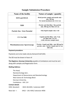


© Copyright 2026