
2D Materials
The AVS Technical Library contains a complete index of complimentary resources available on MyAVS to AVS Members when they login. If you are not an AVS Member and would like access to the AVS Technical Library, click here to join. Table of Contents Presentations on Demand AVS 59 (2012) AVS 60 (2013) AVS 61 (2014) ALD 2011 ALD 2012 ALD 2013 Books and Monographs Videos AVS International Symposia Virtual Programs AVS 59 Presentations on Demand Index Access AVS Presentation on Demand: To access the following Presentations on Demand, please login to MyAVS and choose Presentations on Demand from the left navigation. If you are not an AVS Member and would like access to the AVS Technical Library, click here to Join. Energy Frontiers Chalcogenide Solar Cells I Research Strategies and Results Toward Improving Thin Film CdTe Photovoltaic Devices Beyond 20% Conversion Efficiency Presented by: Timothy Gessert, National Renewable Energy Laboratory Crossover from Intergranular Hopping to Conventional Charge Transport in Pyrite FeS2 Thin Films Presented by: Xin Zhang, University of Minnesota Chalcogenide Solar Cells II Materials and Process Options for Cu(InGa)Se2 Thin Film Solar Cells Presented by: William Shafarman, University of Delaware Thin Film, Heterostructured, and Organic Solar Cells Novel, Single-Crystalline-like Silicon on Low-Cost, Flexible Substrates for High Efficiency Thin Film Photovoltaics Presented by: Venkat Selvamanickam, University of Houston Non-Radiative Carrier Recombination in InGaAs/GaAsP Strain-Balanced Superlattice Solar Cell Presented by: Taketo Aihara, University of Miyazaki, Japan Piezoelectric Photothermal Spectra and Carrier Nonradiative Recombination in InGaAs/GaAsP Super Lattice Structured Solar Cells Presented by: Tetsuo Ikari, University of Miyazaki, Japan Batteries and Fuel Cells Advanced Polymer Electrolyte Materials for Fuel Cell Applications Presented by: Andrew Herring, Colorado School of Mines Organic/Inorganic Composite Materials as Anodes for Lithium Ion Batteries Presented by: Sibani Lisa Biswal, Rice University Plasmas for Photovoltaics and Energy Applications Raman Study of the Properties of Free Standing Silicon Nanocrystals Using Laser Induced Thermal Heating Presented by: Lihao Han, Delft University of Technology, Netherlands Characterization of Energy Materials and Systems Growth Temperature and Stoichiometry Effects on the Inherent Stability of CdS/CdTe Solar Cells Presented by: David Albin, National Renewable Energy Laboratory Photocatalysis and Solar Fuels Doping Effects on the Electronic Structure of Graphitic C3N4 Photocatalysts: Insights from First Principles Presented by: Sebastian Zuluaga, University of Central Florida Energy Frontiers Poster Session The Investigation of the Shunt Resistance using Conductive AFM and EL Measurements in Si Based Thin Film Solar Cells Presented by: Minho Joo, LG Electronics Advanced Research Institute, Republic of Korea Growth Methods and Applications of SiC Nanopowder and Nanowhiskers Presented by: Rajnish Dhiman, University of Southern Denmark Epitaxial Growth of ZnInON Films for Piezo-Electric-Field Effect MQW Solar Cells Presented by: Koichi Matsushima, Kyushu University, Japan Electron Transport at the Nanoscale Electron Transport at the Nanoscale: Nanowires and Junctions Probing Surface-Independent Minority Carrier Transport in Semiconductor Nanowires using Kelvin Probe Microscopy Presented by: Afsoon Soudi, Washington State University Electron Transport at the Nanoscale: Molecules and Defects Electron Localization in Single Mixed-Valence Molecules Presented by: Rebecca Quardokus, University of Notre Dame Transport and Mechanical Properties of Molecular Junctions formed by Acetophenon Deposited on Si (100) Surface Presented by: Ondrej Krejci, Institute of Physics of ASCR, Czech Republic Electron Transport at the Nanoscale: Development of Theories and Techniques Quantum Degeneracy Revealed by the Relation between the Tunneling Current and the Chemical ForceInternal Fields and Presented by: Pavel Jelinek, Institute of Physics of ASCR, Czech Republic Graphene and Related Materials Graphene Growth Spatial Confinement of Epitaxy of Graphene on Microfabricated SiC to Suppress Thickness Variation Presented by: Hirokazu Fukidome, RIEC, Tohoku Univ., Japan Three-Dimensional Graphene Architecture Growth and Its Facile Transfer to Three-Dimensional Substrates Presented by: Ji-Hoon Park, Sungkyunkwan University, Republic of Korea Electronic Properties and Charge Transport Tuning Electronic Properties of Graphene by Controlling its Environment Presented by: Kirill Bolotin, Vanderbilt University The Adsorption of Molecules with Large Intrinsic Electrostatic Dipoles on Graphene Presented by: Lingmei Kong, Univ. of Nebraska-Lincoln Growth of and Interactions in Epitaxial Graphene Layers Presented by: Eli Rotenberg, Lawrence Berkeley National Laboratory Graphene Characterization Including Microscopy and Spectroscopy High Resolution Real and Reciprocal Space Photoelectron Emission Microscocopy on Heterogeneous Graphene/SiC(000-1) Presented by: Konrad Winkler, 1Omicron NanoTechnology, Germany Evidence of Nanocrystalline Semiconducting Graphene Monoxide during Thermal Reduction of Graphene Oxide in Vacuum Presented by: Carol Hirschmugl, University of Wisconsin Milwaukee Chemically-resolved Interface Structure of Epitaxial Graphene on SiC(0001) Presented by: Jonathan Emery, Northwestern Univ. Graphene Surface Chemistry, Functionalization, Biological and Sensor Applications Structural Analysis of Chemically Functionalized Epitaxial Graphene with High-Resolution X-ray Reflectivity Presented by: Michael Bedzyk, Northwestern University Dopants and Defects in Graphene; Graphene Interfaces with Other Materials Increasing Interface Bonding and Tuning Doping Behavior at Metal-Graphene-Metal Sandwich Contact Presented by: Cheng Gong, The University of Texas at Dallas Bi-layer Graphene Growth on Ni(111): The Role of Monolayer Graphene Rotation Presented by: Arjun Dahal, University of South Florida Graphene Nanostructures Crystalline and Electrical Properties of Vertically-Laminated Carbon Nanowalls formed by Two-Step Growth Method Presented by: Hiroki Kondo, Nagoya University, Japan Surface Modification of Vertically Oriented Graphene Electrochemical Double-Layer Capacitors Presented by: Ronald Quinlan, Naval Surface Warfare Center, Carderock Division Beyond Graphene: BN and Other 2D Electronic Materials; 2D Heterostructures X-ray Photoelectron Spectroscopy Investigation of the Valence and Conduction Band Offset at Hexagonal aBN:H/Si Interfaces Presented by: Sean King, Intel Corporation Graphene Device Physics and Applications Graphene and Dielectric Integration: A Sticky Situation? Presented by: Virginia Wheeler, U.S. Naval Research Laboratory Achieving Scaled Dielectrics on Graphene Using Atomic Layer Deposition Presented by: Srikar Jandhyala, University of Texas at Dallas Graphene and Related Materials Poster Session Using Raman Spectroscopy and X-ray Photoelectron Spectroscopy to Guide the Development of GrapheneBased Materials Presented by: Tim Nunney, Thermo Fisher Scientific, UK Dry Transfer of Graphene to Organic and Inorganic Substrates Presented by: Evgeniya Lock, Naval Research Laboratory In Situ Microscopy and Spectroscopy In Situ Spectroscopic Studies of Catalysis and Gas-Solid Reactions In Situ Soft X-ray Photon-in/Photon-out Spectroscopy of Photo-electrochemical Reactions of Hematite in Water Splitting Presented by: Jinghua Guo, Lawrence Berkeley National Lab Probing Nitrogen and Metal Speciation in Non-Platinum Electrocatalysts by Ambient Pressure X-ray Photoelectron Spectroscopies and DFT Calculations Presented by: Kateryna Artyushkova, The University of New Mexico Resolving Growth of Palladium Nanocatalysts Using In Situ FT-IR, XAS and PDF under Practical Atomic Layer Deposition Conditions Presented by: Yu Lei, Argonne National Laboratory In Situ Study of the Oxidation of CO over Ir(111) Presented by: Joachim Schnadt, Lund University, Sweden In Situ Studies of Organic and Soft Materials and In Situ Microscopy In Situ Real Time Examination of the Thin Film Growth of Pentacene on Polymeric Dielectrics Using X-Ray Synchrotron Radiation: Unexpected Changes in the Evolution of Surface Morphology with Substrate Presented by: James Engstrom, Cornell University In Situ, Real-Time Diagnostics of Colon Cancer and Inflammatory Bowel Diseases by Direct Combination of Endoscopy and Rapid Evaporative Ionization Mass Spectrometry Presented by: Zoltan Takats, Imperial College, UK Nanocrystal Phase Transformations in ZBLAN Glass Ceramics Presented by: Jacqueline Johnson, University of Tennessee Space Institute In Situ Characterization of Solids: Film Growth, Defects, and Interfaces Understanding the Dynamic Electronic Properties of Electrode Materials by In Situ X-ray Absorption Spectroscopy Presented by: Michael Bagge-Hansen, Lawrence Livermore National Laboratory In Situ Studies of Al2O3 ALD Growth and Self-cleaning on III-V Surfaces by STM and XPS Presented by: Leonard Rodriguez, IMEC, Belgium Nanomanufacturing Science and Technology Metrology and Environmental Issues in Nanomanufacturing Atomic Layer Deposition Monitored and Characterized by Joint In Situ Real-Time Spectroscopic Ellipsometry and Direct Surface Analysis Presented by: Marcel Junige, Technische Universit?t Dresden, Germany An Integrated Approach Toward Understanding the Environmental Fate, Transport, Toxicity and Occupational Health Hazards of Nanomaterials Presented by: Vicki Grassian, University of Iowa ALD and Scalable Processes for Nanomanufacturing From R&D Towards Industrial Atomic Layer Deposition: Challenges in Scaling up Presented by: Matti Putkonen, Beneq Oy, Finland Migration to ALD Techniques in the Semiconductor Industry: Pattern Effects, Microloading and Film Thickness Variability in Dielectric Thin Films Deposition Presented by: Michael Belyansky, IBM Semiconductor R&D Center Interface Analysis of PEALD TaCN Deposited on HfO2 using Parallel Angle Resolved X-ray Photoelectron Spectroscopy for sub-20nm Gate Last CMOS Transistors Presented by: Fabien Piallat, ST Microelectronics, France Atmospheric Pressure Atomic Layer Deposition of Al2O3 using Trimethylaluminum and Ozone Presented by: Moataz Bellah Mousa, North Carolina State University An Industrial Solution for Surface Passivation of c-Si using Al2O3 Film Deposited by In-line Atmosphere Chemical Vapor Deposition Presented by: Kristopher Davis, University of Central Florida Oxide Heterostructures-Interface Form and Function Structure-Property Relationships in Epitaxial Oxide Interfaces Structural Characterization of Heterojunction n-ZnO/p-NiO Thin Films Epitaxially Deposited on (0002)Al2O3 Substrates Presented by: Yong Hun Kwon, Sungkyunkwan University, Republic of Korea Fabrication and Characterization of Titanium Oxide Films with Tunable Stiffness Presented by: Sidney Cohen, Weizmann Institute of Science, Israel Scanning Probe Microscopy Advances in Scanning Probe Imaging Functional Imaging of Jahn-Teller Dynamics at the Single-molecule Scale Presented by: Joonhee Lee, University of California, Irvine Atomic and Chemical Resolution of Heterogeneous 1-D Metallic Chains on Si(100) by Means of nc-AFM and DFT Presented by: Martin Ondracek, Institute of Physics of ASCR, Czech Republic Characterizing the Best Tips for NC-AFM Imaging on Metal Oxides with Force Spectroscopy and Theoretical Simulations Presented by: Ruben Perez, Universidad Aut?noma de Madrid, Spain Probe-Sample Interactions, Nano-Manipulation and Fabrication Acetylene on Cu(111): Imaging a Molecular Pattern with a Constantly Rearranging Tip Presented by: Yeming Zhu, University of California Riverside Emerging Instrument Formats Atomic Imaging with Peak Force Tapping Presented by: S.C. Minne, Bruker AFM Simultaneous Scanning Tunneling and Atomic Force Microscopy with Subatomic Spatial Resolution Presented by: Franz J. (FJ.) Giessibl, University of Regensburg Scanning Probe Microscopy Poster Session Quantitative Barrier Height Measurements of Tryptanthrin Monolayers on HOPG Presented by: Krishnan Sriraman, Florida Institute of Technology Transparent Conductors and Printable Electronics Transparent Conductors and Devices Surface Functionalization of Amorphous Zinc Tin Oxide Thin Film Transistors Presented by: Gregory Herman, Oregon State University Printable and Flexible Electronics Metal Oxides and Organic Materials for Printed Electronics Presented by: Antonio Facchetti, Polyera Corp. and Northwestern U. Ion Dependence of Gate Dielectric Behavior of Beta-Aluminas in Transparent Oxide Field-Effect Transistors Presented by: Yu Liu, Johns Hopkins University AVS 60 Presentations on Demand Index Access AVS Presentation on Demand: To access the following Presentations on Demand, please login to MyAVS and choose Presentations on Demand from the left navigation. If you are not an AVS Member and would like access to the AVS Technical Library, click here to Join. APT Analysis of Semiconductor, Magnetic, and Oxide Materials Atom Probe Analyses of Interfaces in Nd-Fe-B Permanent Magnets for Higher Coercivity Presented by: Tadakatsu Ohkubo, National Institute for Materials Science, Japan APT and FIM Analysis of Catalysts and Nanoscale Materials In-Situ Environmental Atom Probe Tomograghy for Studying Gas-Solid Reaction in Extreme Environments: Instrumentation and Results Presented by: Santoshrupa Dumpala, Iowa State University Atomic Scale Characterisation of Catalyst Material Presented by: Tong Li, Oxford University, UK From Field Ion Microscopy of Tips to 3D Atom Probe Tomography of Real Catalyst Nanoparticles Presented by: Norbert Kruse, Université Libre de Bruxelles, Belgium Aspects of Helium Ion Microscopy Poster Session Helium Ion Microscopy and Ionoluminescence of Defects Presented by: Gregor Hlawacek, University of Twente, Netherlands Imaging Nascent Soot Particles: Tiniest Soot Particles are Not Structurally Homogeneous Presented by: Sydnie Lieb, University of Southern California Atom Probe Tomography Poster Session Advantage of NbTiN over NbN in Superconducting Properties of Ultra-thin Films Presented by: Marek Guziewicz, Institute of Electron Technology, Poland Basics of Helium Ion Microscopy Monte Carlo Simulations of Helium and Neon Ions Beam Induced Deposition and Etching Presented by: Rajendra Timilsina, The University of Tennessee Knoxville Beyond Graphene: Other 2D Electronic Materials and their Heterostructures Functionalization of MoS2 Surfaces for High-k Atomic Layer Deposition Presented by: Stephen McDonnell, University of Texas at Dallas Electronic and Optical Properties of MoS2 at Monolayer Thickness Presented by: Tony Heinz, Columbia University Low Energy Ion Scattering Studies of the Surface Termination of the Topological Insulator, Bi2Se3 Presented by: Jory Yarmoff, University of California, Riverside Dopants, Defects and Interfaces in 2D Materials Epitaxial Graphene Bands and Adsorption of FePc for Stepped SiC-Si Surfaces Presented by: Jack Rowe, North Carolina State University Education for Interactive R&D & Industrial Implementation 21st Century Skills and Educating the Next Generation Workforce for Expedited Innovation and Deployment Presented by: Christine Broadbridge, Southern Connecticut State University Energy Frontiers Poster Session Angle-Resolved X-Ray Photoelectron Spectroscopy of Iron (II) Fluoride upon Lithiation as a Conversion Reaction Battery Material Presented by: Ryan Whitcomb (Rutgers Department of Physics and Astronomy Summer REU Program); Ryan Thorpe, Sylvie Rangan, Robert Bartynski (Rutgers, The State University of New Jersey) Electrodeposition and Sol-Gel Derived Nitrogen Doped Nanostructured ZnO Thin Films for Possible Use in Photoelectrochemical Splitting of Water Presented by: Nirupama Singh, Deemed University, India Energy Past, Present, and Future Extremes of Heat Conduction in Molecular Materials Presented by: David Cahill, University of Illinois at Urbana Champaign Graphene and Other 2D Materials Poster Session Characterization of Coatings for Tribological and High Temperature Applications Presented by: S. Vijayalakshmi, Vishwanath Thippesamy, M.R. Sridhar, K.A. Harsha, Rupesh Roshan (GE Global Research, India); Barry Record (GE) Growth of 2D Materials A Universal Scheme to Convert Aromatic Monolayers Into Functional Carbon Nanomembranes Presented by: Andrey Turchanin, University of Bielefeld, Germany Graphene-based, Graphene-derived, and New Carbon Materials Presented by: Rodney Ruoff, The University of Texas at Austin Imaging and Lithography with Helium Ions Characterization of 2D Materials by using Scanning Helium Ion Microscopy Presented by: Hongxuan Guo, National Institute for Materials Science, Japan Helium Ion Microscopy of Blood Clot Microstructure Presented by: Stuart Boden, University of Southampton, UK Interfacial Challenges in Nanostructured Solar Cells Interfacial Engineering in ZnO/CdS/CdSe Extremely Thin Absorber (ETA) Solar Cells Presented by: Michael E. Edley, Drexel University Plasmonic Sensing of Dye Impregnation Kinetics of Dye Sensitized Solar Cells (DSSC) Presented by: Bengt Kasemo, Chalmers University of Technology, Sweden Ions at Aqueous Interfaces Specific Ion Effects on Acid-Base Equilibria at the Planar Silica/Water Interface Presented by: Julianne M. Gibbs-Davis, University of Alberta, Canada Dielectric Interfacial Effects Presented by: Roland Netz, FU Berlin, Germany IPF 2013-Manufacturing Challenges for Emerging Technologies From Quanta to the Continuum: Opportunities for Mesoscale Science Presented by: George Crabtree, Argonne National Laboratory Manufacturing Challenges of Directed Self-Assembly Presented by: Roel Gronheid, IMEC, Belgium Microfluidics for Chemical Analysis Presented by: Liz Carr, Agilent Technologies Materials Discovery and Optimization through Iterative Approaches Accelerated Optimization of Solar Cell Materials Presented by: Andriy Zakutayev, National Renewable Energy Laboratory Microstructural and Interface Analysis of Metals Subjected to Various Conditions The Renaissance in Metallurgical Design and the Role of Atom Probe Microscopy Presented by: Simon Ringer, The University of Sydney, Australia Atom Probe Analysis and Challenges to Study a High-k Dielectric Grown on GaN Presented by: Baishakhi Mazumder, University of California, Santa Barbara Novel Synthesis Approaches and Innovative Characterization Techniques Coupled with Theory & Computations Poking Tips at Surfaces: Mechanical and Electronic Properties of Atomically Defined Interfaces Presented by: Peter Grutter, McGill University, Canada Optical, Magnetic, Mechanical and Thermal Properties of 2D Materials Long-range Magnetic Order in a Purely Organic 2D Layer Adsorbed on Epitaxial Graphene Presented by: Amadeo Vazquez-de-Parga, Universidad Autónoma de Madrid, Spain Graphene Nano-Photonics and Carrier Dynamics Presented by: Pablo Alonso González Plasma Processing, Surface Chemistry, Functionalization, and Sensor Applications of 2D Materials Carbon Monoxide-induced Reduction and Healing of Graphene Oxide Presented by: Stephen Weeks, Colorado School of Mines Spectroscopic Ellipsometry for Photovoltaics and Instrument Development Expanded Beam Spectroscopic Ellipsometry for In-line Monitoring of Thin Film Process Presented by: Miklos Fried, Hungarian Academy of Science, Hungary Vibrational Properties of Lanthanum Aluminate and Magnesium Aluminate Spinel Using Fourier Transform Infrared Ellipsometry Presented by: Travis Willett-Gies, New Mexico State University Spectroscopic Ellipsometry: Perspectives and Novel Applications Spectroscopic Ellipsometry – A Perspective Presented by: David Aspnes, North Carolina State University Spectroscopic Ellipsometry of Thin Films for Archival Optical Data Storage and for Microfabricated Thin Layer Chromatography Plates Presented by: Matthew Linford, Brigham Young University Theoretical and Computational Methods Application of Computational Methods to Material Design and Discovery Presented by: Susan Sinnott, University of Florida New Ferroelectrics and Antiferroelectrics by Design Presented by: Karin Rabe, Rutgers, the State University of New Jersey Computational Design of Materials for Catalysis: Interface Matters Presented by: Talat Rahman, University of Central Florida Theory, Computation and Data-Enabled Scientific Discovery High-throughput Quantum Chemistry and Virtual Screening for Materials Solutions Presented by: Mathew Halls, Schrödinger Inc. Computational Materials Design: Precious Metal Free Catalyst for NO Dissociation Presented by: Hideaki Kasai, Osaka University, Japan Thin Film, Organic, and Chalcogenide Solar Cells Surface Energetics of AgInSe2 Thin Films Presented by: Pamela Peña Martin, University of Illinois at Urbana Champaign Thin Films for Energy ALD of Nanolayers and Nanoparticles for Photovoltaics and Other Clean Energy Technologies Presented by: Erwin Kessels, Eindhoven University of Technology, Netherlands Microstructural and Chemical Features Affecting the Reversible Lithiation of SiOx Presented by: Branden Kappes, Colorado School of Mines AVS 60th Past Presidents Panel Video Presented by: Paul Holloway, Joseph Greene, Fred Dylla, Bill Sproul, Dawn Bonnell, and Gregory Exarhos AVS 61 Presentations on Demand Index To access the following Presentations on Demand, please login to MyAVS and choose Presentations on Demand from the left navigation. If you are not an AVS Member and would like access to the AVS Technical Library, click here to Join. 2D Materials Growth and Processing Influence of Substrate Orientation on the Growth of Graphene on Cu Single Crystals Presented by: Tyler Mowll, University at Albany-SUNY Dopants, Defects, and Interfaces in 2D Materials Cutting and Assembling 2 Nanometer Voids in Single Layer Hexagonal Boron Nitride Presented by: Thomas Greber, University of Zurich, Switzerland 2D Materials: Surface Chemistry, Functionalization, Bio and Sensor Applications How Fluorination Enhances Friction Forces for Graphene Presented by: Xin Liu, University of Pennsylvania The Mechanochemistry of Chemically Modified Graphene Presented by: Jonathan Felts, Naval Research Laboratory 2D Materials Characterization including Microscopy and Spectroscopy Influence of Chemisorbed Oxygen on the Growth of Graphene on Cu(100) and Cu(111) by Chemical Vapor Deposition Presented by: EngWen Ong, University at Albany-SUNY Novel Materials Properties at Atomically Thin Limit Presented by: Zhi-Xun Shen, Stanford University Novel 2D Materials Silicene and Germanene: Novel Graphene-like Artificial Silicon and Germanium Allotropes Presented by: Guy Le Lay, Aix-Marseille University, France Silicon Growth at the Two-Dimensional Limit on Ag(111) Presented by: Andrew Mannix, Northwestern University Growth, Structure, and Properties of 2D SiO2Polymorphs Presented by: Eric Altman, Yale University Nanostructures including 2D Heterostructures, Patterning of 2D Materials Gate Tunable Carbon Nanotube - Single Layer MoS2 p-n Heterojunctions Presented by: Deep Jariwala, Northwestern University Exceptional Ballistic Conduction in Epitaxial Graphene Nanoribbons Presented by: Walt de Heer, Georgia Institute of Technology Novel Quantum Phenomena in 2D Materials Use of XPS for Device Characterization Presented by: Sefik Suzer, Bilkent University, Turkey 2D Materials Poster Session Modification of Density of States in Iron Chloride Intercalated Epitaxial Graphene with Electric Bias Presented by: Michael Williams, Clark Atlanta University Enhanced Electrical Conductivity of Transparent Carbon Nanotube Sheet by Acid Treatment Presented by: Jinhong Kim, University of Texas at Dallas Studying Graphene & Other 2D Materials With A Multiprobe Cryogenic System That Provides For Simultaneous Raman & Other Optical Modalities With A Wide Variety of Functional SPM Probes Presented by: Aaron Lewis, Hebrew University of Jerusalem, Israel Conservation Studies of Heritage Materials Parylene Coating for Paper/Book Strengthening Presented by: Lei Pei, Johns Hopkins University Iron Gall Ink Chemistry and Corrosion of Historical Documents Probed by XPS and Raman Presented by: Karen Gaskell, University of Maryland, College Park Conservation Studies of Heritage Materials 2 A Conservator’s Perspective of Technical Studies and Scientific Analysis Presented by: Patricia Favero, The Phillips Collection The Degradation Mechanisms of Cadmium Pigments in Works by Henri Matisse, Edward Munch, and Their Contemporaries Presented by: Jennifer Mass, Winterthur Museum The Analysis of Egg-Oil Binding Media by Time-of-Flight Secondary Ion Mass Spectrometry Presented by: Zachary Voras, University of Delaware Conservation Studies of Modern Heritage Materials 3 Faces from the Past: Microbeam Imaging and Analysis of Artifacts from ancient Mesoamerica Presented by: Timothy Rose, Smithsonian Institution Atomic Layer Deposited Diffusion Barriers on Non-ideal Silver and Bronze Cultural Heritage Objects Presented by: Amy Marquardt, University of Maryland, College Park Energy Harvesting with Nanostructures Triboelectric Nanogenerator - A New Energy Technology Presented by: ZhongLin Wang, Georgia Institute of Technology Conflicting Roles of Charge Traps in ETA Solar Cells: The CREM Point of View Presented by: Hagai Cohen, Weizmann Institute of Science, Israel Stack Numbers Dependence of the Activation Energies for Carrier Escape from and Recombination in StrainBalanced InGaAs/GaAsP MQW Presented by: Atsuhiko Fukuyama, University of Miyazaki, Japan Fuel Formation and Thermal Transport Atomistic Insights as the the pH Dependence of Onset Potential of the Oxygen Evolution Reaction on Hematite Presented by: Anders Hellman, Chalmers University, Sweden The Effect of Particle Size and Surface Termination of n-Si on Thermal and Electrical Conductivity Presented by: Thomas Lopez, University of California - Riverside Charge Storage Materials and Devices Spatiotemporal Investigation of Li-Air Battery under Operating Condition: Understanding the Cathodic and Anodic Electrochemical Processes and their Interdependence Presented by: Di-Jia Liu, Argonne National Laboratory Solid Micro-supercapacitor using Directed Self-Assembly of Tobacco Mosaic Virus and RuO2 Presented by: Markus Gnerlich, University of Maryland, College Park Charged Particles Micro-Penning-Malmberg Trap: An Approach to Store High Densities with Substantially Lower End Barrier Potentials Presented by: Alireza Narimannezhad, Washington State University Energy Frontiers Poster Session Mini-band Formation in a Strain-balanced InGaAs/GaAsP MQW Solar Cell Structure Investigated by a Photoreflectance and a Surface Photovoltage Spectroscopy Presented by: Tetsuo Ikari, University of Miyazaki, Japan Vacuum Deposition Of Photosystem 1 Films In P-Doped Silicon Surface To Improve The Efficiency Of BioPhotovoltaic Cells Presented by: Carlos Felipe Rezende Facchini, University of Campinas, Brazil Thin Film Photovoltaics Epitaxy and Nanochemistry of CdS on Cu(In,Ga)Se2 for Photovoltaic Devices Presented by: Angus Rockett, University of Illinois at Urbana Champaign Improvement of SnS-based Photovoltaic Devices via Reverse Engineering of the Voc and Study of Optimal nType Material Presented by: Rona Banai, Penn State University Micro-Structural Activation Mechanisms in Thin Film CdTe Photovoltaic Devices Presented by: John Walls, Loughborough University, UK Organic-Inorganic Interfaces for Energy Towards Efficient Solution Processed Organic Photovoltaic Devices Presented by: Elsa Reichmanis, Georgia Institute of Technology Ambient Pressure X-ray Photoelectron Spectroscopy (APXPS) Studying Zeolites and Clays with the Tools of Surface Science from UHV to Near-Ambient Pressures Presented by: Jorge Boscoboinik, Brookhaven National Laboratory Environmental Electron Microscopies Nanocrystal Shape Evolution during Growth Presented by: Haimei Zheng, Lawrence Berkeley Lab, University of California, Berkeley Selective Staining for Enhanced Spectroscopic Identification of Domains in Immiscible Polymer Blends by Micro-Raman Spectroscopy Presented by: Nicholas Heller, SUNY Stony Brook In-Situ X-ray Absorption and Raman Spectroscopy Photoelectron Spectroscopy on Ice, Mineral Oxides and Aqueous Solutions of Atmospheric Relevance Presented by: Markus Ammann, Paul Scherrer Institut, Switzerland In Situ Analysis of Materials Under Mechanical Stress: A Novel Instrument for Simultaneous Nanoindentation and Raman Spectroscopy Presented by: Chris Michaels, NIST Characterization of 3D Structures, 2D films and Interconnects LEIS Characterization of the Outer Surface, Ultra-Thin Layers and Contacts Presented by: Hidde Brongersma, ION-TOF / Tascon / Calipso, Netherlands Characterization of III-Vs (2:00-3:20 pm)/Photovoltaics, EUV masks, etc. (3:40-4:40 pm) Characterization of Ag/CuInSe2 Thin-Film Photovoltaics by Photoelectron Spectroscopy Presented by: Pinar Aydogan, Bilkent University, Turkey Imaging of the Native Inversion Layer on Silicon-on-Insulator via Scanning Surface Photovoltage; Implications for RF harmonic generation Presented by: Daminda Dahanayaka, IBM Synchrotron Studies of Processes in Energy Conversion, Electronic Devices and Other Materials I In Situ Study of Plasma Assisted Atomic Layer Epitaxy of III-N Semiconductors Using Synchrotron X-ray Methods Presented by: Charles Eddy, Jr., Naval Research Laboratory Synchrotron Studies of Processes in Energy Conversion, Electronic Devices and Other Materials II Synchrotron-based In Situ Study of PEMFC, SOFC, Battery and Supercapacitor Components Presented by: Benedetto Bozzini, Universita' del Salento - Italy Synchrotron-Based Spectroscopy Shedding Light on Solar Cells Presented by: Franz Himpsel, University of Wisconsin-Madison Soft X-ray Spectroscopy for Fundamental Understanding and Practical Optimization of Battery Materials Presented by: Wanli Yang, Lawrence Berkeley National Laboratory Free Electron Laser and Synchrotron Studies at the Molecule-Surface Interfaces Layer Speciation and Electronic Structure Investigation of Hexagonal Boron Nitride Thin Film by Scanning Transmission X-ray Microscopy Presented by: Jian Wang, Canadian Light Source Inc., Canada Synchrotron Analysis Poster Session Soft X-ray Spectroscopy Reveals Chemical Information beneath the Surface of Organic Photovoltaic Devices Presented by: Claudia Fleischmann, IMEC, Belgium Plasma Processing of Antimicrobial Materials and Devices Plasma Polymers: Dogma, Characteristaion and Challenges Presented by: Sally McArthur, Swinburne University of Technology, Australia Plasma Processing of Biomemetic Materials Biofunctionalization of Surfaces by Energetic Ion Implantation: Fundamentals and Recent Progress on Applications Presented by: Marcela Bilek, University of Sydney, Australia Probing Chemical Reactions at the Nanoscale Surface Structures of Catalysts in Reactive Environments with Scanning Tunneling Microscopy Presented by: Luan Nguyen, University of Kansas Scanning Probe Microscopy Poster Session Cross Sectional Mapping of CdTe PV Devices with Scanning Capacitance Microscopy Presented by: Gilad Zorn, GE Global Research Center Probe-Sample Interactions and Emerging Instrument Formats 2013 ASSD Student Award Talk: New Insights into Nanoscale Adhesion from In Situ TEM Studies Presented by: Tevis Jacobs, University of Pennsylvania Photocatalysis and Photochemistry at Surfaces Infrared Reflection-Absorption Spectroscopy Study of Adsorption and Photo-Decomposition of Formic Acid on Reduced and Defective Rutile TiO2 (110) Surfaces Presented by: Andreas Mattsson, Uppsala University, Sweden Atomistic Modeling of Surface Phenomena Oxidation of Cu Surfaces with Step-Edge Defects: Insights from Reactive Force Field Simulation Presented by: Qing Zhu, University of Pittsburgh The Role of Time-scale Analysis in Simulation of ALD and CVD Surface Reaction Kinetics Presented by: Raymond Adomaitis, University of Maryland, College Park Real-Time Ab-Initio KMC Simulation of the Self-Assembly and Sintering of Bimetallic Epitaxial Nanoclusters: Au+Ag on Ag(100) Presented by: James Evans, Iowa State University ALD 2011 Presentations on Demand Index Access AVS Presentation on Demand: To access the following Presentations on Demand, please login to MyAVS and choose Presentations on Demand from the left navigation. If you are not an AVS Member and would like access to the AVS Technical Library, click here to Join. ALD 2011 Session A Session A: Electronics I The Nature of the III-V/Oxide Interface and its Impact on the ALD Growth of High-k Dielectrics for Advanced CMOS Presented by: M. Pemble, E. O'Connor, Tyndall National Institute, Univ. College Cork; A. O'Mahony, Cambridge Nanotech, Inc.; B. Brennan, Dublin City Univ.; V. Djara V, C. Azzolini, K. Cherkaoui, S. Monaghan, R. Nagle R, I.M. Povey, A. Blake, Tyndall National Institute, Univ. College Cork; R. Contreras, Centro de Investigación y de Estudios Avanzados del IPN; M. Milojevic, The Univ. of Texas at Dallas; G. Hughes, Dublin City Univ.; R.M. Wallace, The Univ. of Texas at Dallas; P.K. Hurley, Tyndall National Institute, Univ. College Cork Semiconductor-Metal Transition in Thin VO2 Films Grown by Ozone Based Atomic Layer Deposition Presented by: G. Rampelberg, Ghent Univ.; M. Schaekers, K. Martens, IMEC; Q. Xie, D. Deduytsche, B. De Schutter, Ghent Univ.; N. Blasco, Air Liquide Electronics; J. Kittl, IMEC; C. Detavernier, Ghent Univ. Atomic Layer Epitaxy of Rare Earth Oxide Films on GaAs(111)A and Their Device Properties Presented by: Y. Liu, Harvard Univ.; M. Xu, Purdue Univ.; J. Heo, Harvard Univ.; P.D. Ye, Purdue Univ.; R.G. Gordon, Harvard Univ. Y2O3 Films Grown by a Novel ALD Process from Y(EtCp)3 and Water Enabling Y-Based Silicates in Direct Contact with Si with Sub-nm EOTs Presented by: C. Dubourdieu, IBM T.J. Watson Research Center and CNRS Paris France; M. Copel, E. Cartier, J. Bruley, M. Hopstaken, S.M. Rossnagel, IBM T.J. Watson Research Center; A. Kellock, IBM Almaden Research Center; M. M. Frank, IBM T.J. Watson Research Center Atomic Layer Deposition of Ultrathin High-ê Dielectrics on Epitaxial Graphene via Fluorine Functionalization Presented by: V. Wheeler, N.Y. Garces, L.O. Nyakiti, R.L. Myers-Ward, G.G. Jernigan, C.R. Eddy Jr, D.K. Gaskill, Naval Research Lab ALD Beryllium Oxide as a High-k Gate Dielectric for III-V MOS Devices Presented by: J. Yum, T. Akyol, M. Lei, D.A. Ferrer, Univ. of Texas at Austin; T.W. Hudnall, Texas State Univ.-San Marcos; M. Downer, C.W. Bielawski, Univ. of Texas at Austin; G. Bersuker, SEMATECH; J.C. Lee, S.K. Banerjee, Univ. of Texas at Austin Session A: Electronics II Novel Semi-batch ALD Technology for ULSI Device Fabrication Presented by: K.H. Lee, D. H. You, H.C. Ha, K.H. Ahn, Wonik IPS Co. Atomic Layer Deposition of MgO for High-k Capping Layers Presented by: F. Tang, ASM, Phoenix; E. Tois, ASM, Helsinki; S-H. Jung, ASM, Phoenix; P. Räisänen, ASM,Phoenix; M. Givens, ASM, Phoenix; J.W. Maes, D. Pierreux, V. Machkaoutsan, ASM, Belgium; M. Tuominen, S. Haukka, ASM, Helsinki HfAlO3 Gate Stack on III-V p-channel Material GaSb: ALD Hf-first Versus Al-first Presented by: C. Wang, M. Xu, J. Zhang, P.D. Ye, Purdue Univ. In-situ Electrical Studies of Ozone Based Atomic Layer Deposition on Graphene Presented by: S. Jandhyala, B. Lee, G. Mordi, J. Kim, The Univ. of Texas at Dallas Evaluation of Novel Precursors for Atomic Layer Deposition of Nb2O5 Thin Films Presented by: T. Blanquart, J. Niinistö, M. Heikkilä, Univ. of Helsinki; C. Xu, W. Hunks, ATMI; M. Ritala, Univ. of Helsinki Copper Films Grown via Copper Oxide ALD Integrated with Different Liner Materials for Interconnect Applications Presented by: T. Waechtler, Chemnitz Univ. of Technology / Fraunhofer ENAS; S. Mueller, L. Hofmann, R. Mothes, Chemnitz Univ. of Technology; S.-F. Ding, Fudan Univ.; S. E. Schulz, Chemnitz Univ. of Technology /, Fraunhofer ENAS; H. Lang, Chemnitz Univ. of Technology; X-P. Qu, Fudan Univ.; T. Gessner, Chemnitz Univ. of Technology / Fraunhofer ENAS Atomic Layer Deposition (ALD) and Chemical Vapor Deposition (CVD) of Copper-Based Metallization for Microelectronic Fabrication Presented by: Y. Au, Y. Lin, H. Kim, Z. Li, R. Gordon, Harvard Univ. Session A: Lighting ZnO-Based Light-Emitting Diodes Grown by Atomic Layer Deposition Presented by: M. Chen, J-J. Huang, J-R. Yang, National Taiwan Univ.; M. Shiojiri, Kyoto Institute of Technology Enabling High Performance Ultraviolet Instruments for Astronomy and Space Exploration with ALD Presented by: F. Greer, M.E. Hoenk, T.J. Jones, B.C. Jacquot, S. Monacos, Jet Propulsion Lab; E. Hamden, D. Schiminovich, Columbia Univ.; S. Nikzad, Jet Propulsion Lab Session A: Precursor Simulation, Modeling, & Theory Mechanism of Noble Metal ALD Presented by: S. Elliott, Tyndall National Institute Fluid Flow Effects in ALD for Semiconductor Manufacturing Presented by: J.P. Trelles, S.S. Liao, Intel Corporation In Situ Gas Phase Measurements and Equipment-Scale Simulations of Metal Alkylamide ALD Processes Presented by: J.E. Maslar, D.R. Burgess, Jr., E.F. Moore, W.A. Kimes, B.A. Sperling, NIST Reaction Modeling During TiN Growth Using TiCl4 and MMH Presented by: K. Narushima, Tokyo Electron Yamanashi Ltd.; S.Y. Kang, Tokyo Electron Ltd.; Y. Kato, Y. Otsuka, Air Water, Inc.; T. Hotta, Tokyo Electron Yamanashi Ltd.; A. Kakimoto, M. Tachibana, Tokyo Electron Tohoku Ltd.; Y. Hanada, Tokyo Electron Yamanashi Ltd. Coupling Ballistic Transport and Surface Reaction Models for Direct Simulation of Conformal ALD Presented by: R. Adomaitis, Univ. of Maryland Session A: Precursors, Precursor Design, & Recipe Development New Volatile Precursors for Group 2 Metals Presented by: J. Norman, M. Perez, M.S. Kim, X. Lei, S. Ivanov, A. Derecskei, L. Matz, I. Buchanan, Air Products High Rate Growth of SiO2 by Thermal ALD Using Tris(dimethylamino)silane and Ozone Presented by: G. Liu, R. Bhatia, E.W. Deguns, M.J. Dalberth, M.J. Sowa, A. Bertuch, L. Lecordier, G. Sundaram,, Cambridge NanoTech, Inc. Plasma-Enhanced ALD of TiO2 Using Cp-Based Precursors and Various Plasma Compositions: Experiments and DFT Calculations Presented by: S.E. Potts, N. Leick, Eindhoven Univ. of Technology; A. Zydor, S. D. Elliott, Tyndall National Institute; W.M.M. Kessels, Eindhoven Univ. of Technology Nitrogen-Mediated ALD of Platinum: Precursor Synthesis, Film Deposition and Mechanistic Insights Presented by: S.B. Clendenning, P.E. Romero, H.S. Simka, A.B. Mukhopadhyay, S. Shankar, Intel Corporation p-Type Phosphorus-doped Zinc Oxide Films Deposited by Atomic Layer Deposition: Microstructural Effects Presented by: W.L. Gladfelter, H. Yuan, B. Luo, S.A. Campbell, Univ. of Minnesota Surface Chemistry of Copper Precursors in Connection with Atomic Layer Deposition (ALD) Processes Presented by: Q. Ma, Univ. of California; R.G. Gordon, Harvard Univ.; F. Zaera, Univ. of California Session A: In-Situ Analysis In Situ X-ray Based Characterization of ALD Processes Presented by: C. Detavernier, J. Dendooven, K. Devloo-Casier, K. De Keyser, D. Deduytsche, Ghent Univ.; S. Pulinthanathu Sree, J. Martens, KULeuven, Leuven, Belgium; K.F. Ludwig, Boston Univ. In-situ Monitoring for ALD Process Control Presented by: J.W. Bartha, M. Knaut, M. Junige, M. Geidel, M. Albert, TU Dresden, Institute of Semiconductor and Microsystems Technology Indium Oxide Atomic Layer Deposition Facilitated by the Synergy between Oxygen and Water Presented by: J. Libera, J. Hryn, J. Elam, Argonne National Lab Session A: Characterization Atomic Layer Deposition of Thin Superconducting Films and Multilayer Meterostructures Presented by: J.A. Klug, Th. Proslier, Argonne National Lab; N.G. Becker, Argonne National Lab and, Illinois Institute of Technology; J.W. Elam, H. Claus, J. Norem, Argonne National Lab; J.F. Zasadzinski, Illinois Institute of Technology; M.J. Pellin, Argonne National Lab Characterization of ALD Coatings in Nanoporous Thin Films by Ellipsometric Porosinetry Presented by: J. Dendooven, Ghent Univ.; S. Pulinthanathu Sree, Catholic Univ. of Leuven; R. Van Hove, K. Devloo-Casier, Ghent Univ.; M. Baklanov, IMEC; J.A. Martens, Catholic Univ. of Leuven; C. Detavernier, Ghent Univ. Microstructural Evolution of Silver Thin Films Deposited by ALD and the Resulting Changes in the Plasmonic Properties Presented by: S.M. Prokes, Naval Research Lab; E. Cleaveland, Naval Research Lab ASEE; O.J. Glembocki, Naval Research Lab; H. Qi, Naval Research Lab ASEE; J. Caldwell, E. Foos, Naval Research Lab; J. Niinistö, Univ. of Helsinki, Finland Innovative Characterization Techniques for MoO3 ALD Coatings Presented by: M. Diskus, O. Nilsen, H. Fjellvåg, S. Diplas, Univ. of Oslo; B. Weckhuysen, Univ. of Utrecht Session A: Solar ALD of SiO2 and Al2O3 for Surface Passivation of c-Si Solar Cells Presented by: W.M.M. Kessels, G. Dingemans, C.A.A. van Helvoirt, M.M. Mandoc, M.C.M. van de Sanden, Eindhoven Univ. of Technology Atomic Layer Deposition and Chemical Vapor Deposition of Tin(II) Sulfide Presented by: P. Sinsermsuksakul, J. Heo, R.G. Gordon, Harvard Univ. Replication of Butterfly Wings by ALD and Nanoimprint for Production of High Efficiency Si Solar Cells Presented by: X. Tang, L. A. Francis, ICTEAM institute, Université catholique de Louvain, Belgium; P. Simonis, Départment de Physique, Facultés Universitaires Notre-Dame de la Paix, Belgium; M. Haslinger, R. Delamare, ICTEAM institute, Université catholique, Belgium; O. Deschaume, IMCN institute, Université catholique de Louvain, Belgium; D. Flandre, ICTEAM institute, Université catholique de Louvain, Belgium; P. Defrance, A. M. Jonas, IMCN institute, Université catholique de Louvain, Belgium; J- P. Vigneron, Départment de Physique, Facultés Universitaires Notre-Dame de la Paix, Belgium; J-P. Raskin, ICTEAM institute, Université catholique Dielectric Backside Passivation Improvements by Si-doped Al2O3 Dielectrics Presented by: F. Benner, S. Kupke, S. Jakschik, E. Erben, Namlab gGmbH Dresden; M. Knaut, IHM TU Dresden; J. Müller, Fraunhofer CNT Dresden; M. Rose, Fraunhofer IKTS Dresden; U. Schroeder, T. Mikolajick, Namlab gGmbH Dresden High Performance Dye-Sensitized Photovoltaic Cells Incorporating Micro-fibers with Conformal TiO2 Coating by Atomic Layer Deposition Presented by: D.H. Kim, M. Woodroof, G. Parsons, NC State Univ. Session A: Catalysis & Fuel Cells Pt-Ru Alloy Catalyst Development by Atomic Layer Deposition for Direct Methanol Fuel Cells Presented by: A. Dameron, NREL; S. Christensen, K. Hurst, T. Olson, NREL; S. Pylypenko, Colorado School of Mines; K O'Neill, J Bult, D. Ginley, NREL; R. O'Hayre, Colorado School of Mines; H. Dinh, NREL Performance Enhancement of Micro-solid Oxide Fuel Cells Fabricated on Nanoporous Anodic Aluminum Oxide Templates by Atomic Layer Deposition Presented by: J.I. Lee, C-W. Kwon, D-J. Lee, Seoul National Univ.; J-W. Son, Korea Institute of Science and Technology; K-B. Kim, Seoul National Univ. ALD of MnOx as a Catalyst for the Splitting of Water Presented by: K.L. Pickrahn, S. Park, S.F. Bent, Stanford Univ. Nucleation & Growth of Continuous & Ultrathin Pt ALD Films for Improved Oxygen Reduction Activity in Fuel Cells Using W ALD Adhesion Layers Presented by: L. Baker, A.S. Cavanagh, S.M. George, Univ. of Colorado, Boulder; A. Kongkanand, F.T. Wagner, General Motors Research & Development, Honeoye Falls, NY Influence of the Precursors Chemistry on the ALD Growth of Cobalt-molybdenum Oxide Films Presented by: M. Diskus, O. Nilsen, H. Hjellvåg, Univ. of Oslo; B. Weckhuysen, Univ. of Utrecht Session A: Batteries & Storage ALD of Al2O3 for Highly Improved Performance in Li-ion Battery Electrodes Presented by: A. Dillon, Y. Jung, NREL; L. Riley, Univ. of Colorado/NREL; A. Cavanagh, Univ. of Colorado; Y. Yan, NREL; S.M. George, Univ. of Colorado Atomic Layer Deposition for Uniform Coating of Biotemplated Nanostructured Electrodes for Lithium-ion Microbatteries Presented by: E. Pomerantseva, K. Gerasopoulos, X. Chen, G. Rubloff, R. Ghodssi, Univ. of Maryland, College Park Engineering LixAlySizO Thin Films as a Solid Electrolyte for 3D Microbatteries Presented by: Y. Perng, J. Cho, D. Membreno, UCLA; M.F. Toney, Stanford Synchrotron Radiation Lightsource, Menlo Park; B. Dunn, J.P. Chang, UCLA ALD of Lithium Containing Compounds Presented by: J. Hamalainen, T. Hatanpaa, J. Holopainen, Univ. of Helsinki; F. Munnik, Helmholtz-Zentrum Dresden-Rossendorf,, Institute of Ion Beam Physics and Materials Research; M. Ritala, M. Leskela, Univ. of Helsinki ALD of Solid-State Electrolytes – A Prerequisite for 3D All-Solid-State Lithium Ion Batteries Presented by: T. Aaltonen, O. Nilsen, H. Fjellvåg, Univ. of Oslo Session A: Energy Devices Concept of Spatially Divided Deep Reactive Ion Etching with ALD-based Passivation Presented by: F. Roozeboom, TNO, Eindhoven and TU Eindhoven, The Netherlands; A.M. Lankhorsta, G. Winands, N.B. Koster, P. Poodt, A. Vermeer, TNO; G. Dingemans, W.M.M. Kessels, Eindhoven Univ. of Technology Ozone Based Atomic Layer Deposition of Polycrystalline V2O5 for Electrochemical Energy Storage Presented by: X. Chen, E.A. Pomerantseva, P. Banerjee, K. Gregorczyk, K. Gerasopoulos, R. Ghodssi, G.W. Rubloff, Univ. of Maryland Highly Active Oxide Photocathode for Photoelectrochemical Water Reduction Presented by: A. Paracchino, V. Laporte, K. Sivula, M. Graetzel, E. Thimsen, Ecole Polytechnique Fédérale de Lausanne Session B Session B: Surface Chemistry & Conformal Coatings I Atomic Layer Deposition of Smooth Phase Change GexSbyTez Layers on Planar and 3D Structures Presented by: L. Yang, U. Weber, P.K. Baumann, AIXTRON SE; J. Mack, G. Kim, Z. Karim, S. Ramanathan, AIXTRON Inc. Comparison of the Conformality of ALD Grown SrTiO3 and BaTiO3 Using H2O or O3 as Oxygen Source Presented by: T. Blomberg, E. Tois, S. Haukka, M. Tuominen, ASM; W. Besling, NXP; B. Riou, C. Bondoux, C. Richard, ST Micro A Quantified-Dosing ALD Reactor with Studies and Applications of Controlled Dosing to the ALD Process Presented by: T. Larrabee, T. Mallouk, D. Allara, Penn State Univ. Conformality of Remote Plasma Enhanced ALD Processes: An Experimental Study Presented by: J. Niinistö, M. Kariniemi, Univ. of Helsinki; M. Putkonen, Beneq Oy; M. Vehkamäki, M. Kemell, M. Ritala, M. Leskelä, Univ. of Helsinki ALD Growth per Cycle Modulation Using Surface Functionalization: A Strategy for Improved Stoichiometry Control and Higher Doping Efficiencies Presented by: A. Yanguas-Gil, J.W. Elam, Argonne National Lab In-Situ Study of the Reaction Mechanism Kinetics of Pt ALD Presented by: I. Erkens, Eindhoven Univ. of Technology; A.J.M. Mackus, H.C.M. Knoops, F. Roozeboom, W.M.M. Kessels, Eindhoven Univ. of Technology Surface Loss in Ozone-based ALD Processes Presented by: H.C.M. Knoops, Eindhoven Univ. of Technology; J.W. Elam, J.A. Libera, Argonne National Lab; W.M.M. Kessels, Eindhoven Univ. of Technology Session B: Surface Chemistry & Conformal Coatings II Oxide Coating of Nanoporous Alumina using ALD to Produce Highly Porous Spinel Presented by: E. Rauwel, O. Nilsen, Univ. of Oslo; J. Walmsley, Sintef Trondheim; M. Diskus, Univ. of Oslo; E. Rytter, Statoil Trondheim; H. Fjellvåg, Univ. of Oslo Non-aqueous Sol-gel Routes Applied to the ALD of Oxides: The Case of Titanium Isopropoxide - Acetic Acid Process Presented by: K. Bernal-Ramos, Univ. of Texas at Dallas, Richardson, USA; C. Marichy, G. Clavel, N. Pinna, CICECO, Univ. of Aveiro, Aveiro, Portugal; Y.J. Chabal, Univ. of Texas at Dallas, Richardson, USA In Situ Ellipsometric Investigations During the ALD Growth of Ru Presented by: M. Junige, M. Knaut, M. Geidel, M. Albert, J. W. Bartha, Dresden Univ. of Technology The Effects of TiO2 Crystallinity on Nucleation in Atomic Layer Deposition of Platinum Presented by: H.-B.-R. Lee, S.F. Bent, Stanford Univ. Flash-ALD – A Novel Approach for Atomic Layer Controlled Growth of Thin Films Induced by Flash Heating Presented by: T. Henke, M. Geidel, M. Knaut, M. Albert, J.W. Bartha, TU Dresden Interface Cleaning During the Atomic Layer Deposition of Metal Oxides on GaAs(100) Surfaces Presented by: T. Gougousi, L. Ye, J.W. Lacis, UMBC In Situ Reaction Mechanism Studies on Atomic Layer Deposition of Ir and IrO2 from Ir(acac)3 Presented by: K. Knapas, M. Ritala, Univ. of Helsinki Using Growth Inhibitors to Enhance Nucleation Density in Low Temperature CVD Presented by: N. Kumar, P. Zhang, A.C. Dunbar, L.M. Davis, G.S. Girolami, J.R. Abelson, S. Babar, Univ. of Illinois at Urbana Champaign Session B: Industrial ALD I Industrial ALD Systems: The Role of Computation in Design Presented by: G. Sundaram, Cambridge NanoTech, Inc.; A. Bertuch, R. Bhatia, M.J. Dalberth, L. Lecordier, G. Liu, M. Sershen, M. Sowa, R. Coutu, J.S. Becker, Cambridge NanoTech, Inc. High Throughput Films and Devices by Spatial Atomic Layer Deposition Presented by: D. Levy, S. Nelson, M. Burberry, L. Tutt, Eastman Kodak Company Studying Roll-to-Roll ALD Process Conditions Using a Moving Substrate under a Gas Source Coating Head Presented by: P.R. Fitzpatrick, Z.M. Gibbs, S.M. George, Univ. of Colorado at Boulder Model-based Methodology for Analysis and Design of ALD Processes Presented by: A. Holmqvist, S. Stenström, Lund Univ. Session B: Industrial ALD II Continuous ALD Deposition on Flexible Substrates – Towards a Roll-to-Roll Process Presented by: P. Maydannik, T.O. Kääriäinen, K. Lahtinen, D. Cameron, Lappeenranta Univ. of Technology Fast Atomic Layer Deposition for High Throughput and Low Temperature Applications Presented by: P. Poodt, A. Illiberi, M. Smets, B. Kniknie, H. Winands, R. Knaapen, TNO; F. Roozeboom, TNO and Eindhoven Univ. of Technology; M. Tijdink, A. van Asten, TNO PEALD Batch Processing of Al doped TiO2 Presented by: W. Lehnert, G. Ruhl, Infineon Technologies AG, Germany; A. Gschwandtner, R3T GmbH, Germany On the Impact of Energetic Photons and Ions on Plasma-assisted ALD of Metal Oxides Presented by: H.B. Profijt, M.C.M. van de Sanden, W.M.M. Kessels, Eindhoven Univ. of Technology Session B: Industrial ALD III High Rate Roll to Roll ALD of Ultra-Barrier Oxide Films Presented by: E. Dickey, Lotus Applied Technology Cost Effective ALD for Solar Cell Passivation with Al2O3: Tool Design and Considerations Presented by: V. Kuznetsov, P.Vermont, E.H.A Granneman, Levitech BV Temperature Window for Al2O3 and ZnO Growth by Atmospheric Pressure ALD Presented by: J.S. Jur, M.B. Mousa, C.J. Oldham, G.N. Parsons, NC State Univ. Roll to Roll ALD: From Prototype to Manufacturing Presented by: M. Dalberth, M. Sershen, G. Sundaram, R. Coutu, J. Becker, Cambridge NanoTech QCM Sensors for Advanced Process and Equipment Control Presented by: M. Knaut, M. Albert, J.W. Bartha, TU Dresden, Institute of Semiconductors and Microsystems Comparison of Structural and Electrical Properties of In-situ Al2O3 Capped and Non-capped La2O3 Layers Deposited on Silicon Presented by: K. Karakaya, IMEC / Holst Centre; C.A. van den Heuvel, Philips Innovation Services; J. Swerts, IMEC VZW; S.H. Brongersma, IMEC / Holst Centre Session B: Nanostructures I Process Integration of Atomic Layer Deposition (ALD) in Nanoenergy Devices Presented by: P. Banerjee, A. Brozena, X. Chen, K. Gregorczyk, K. Gerasopoulos, L. Haspert, S. Sherrill, Y. Wang, R. Ghodssi, Univ. of Maryland; S.B. Lee, Korea Advanced Institute of Science and Technology; G.W. Rubloff, Univ. of Maryland An Approach for Cu ALD via Reduction of Ruthenium-Containing CuxO Films for the Metallization in Spintronic and ULSI Interconnect Systems Presented by: S. Mueller, Chemnitz Univ. of Technology, Center for Microtechnologies (ZfM), 09107 Chemnitz, Germany ALD Metal/Oxide Nanoelectrode Arrays for Hybrid Organic/Inorganic Photovoltaic Devices Presented by: D. Gu, H. Baumgart, G. Namkoong, Old Dominion Univ. (Sn,Al)Ox Films Grown by Atomic Layer Deposition Presented by: J. Heo, Y. Liu, P. Sinsermsuksakul, Z. Li, L. Sun, W. Noh, R.G. Gordon, Harvard Univ. Tailor-Made Superparamagnetic Nanotubes for Novel Hybrid Ferrofluid Suspensions Presented by: R. Zierold, Univ. of Hamburg; Z. Wu, Ulm Univ.; J. Bachmann, Univ. of Hamburg; C.E. Krill III, Ulm Univ.; K. Nielsch, Univ. of Hamburg Session B: Nanostructures II ALD for Textiles Presented by: J.S. Jur, J.C. Halbur, B. Gong, C.J. Oldham, W.J. Sweet, III, K. Lee, J.C. Spangola, B. Pourdeyhim, G.N. Parsons, NCSU Characteristics of Sb-rich GeSbTe (GST) Thin Films Grown by Atomic Layer Deposition for High Performance Phase Change Random Access Memory (PCRAM) Presented by: K. Lee, B.M. Seo, J.M. Lee, K. Hong, S.K. Park, Hynix Semiconductor Inc. Oxidation Behavior of Cu Nanoparticles Embedded in Porous Alumina Films Produced by Molecular Layer Deposition Presented by: Y. Qin, Max-Planck-Institute of Microstructure Physics; Y. Yang, Institute of Microsystems Engineering (IMTEK), Albert-Ludwigs-Univ. Freiburg; R. Scholz, M. Knez, Max-Planck-Institute of Microstructure Physics Controlling the Nucleation of Noble Metal ALD and its Application to Nanopatterning Presented by: A.J.M. Mackus, Eindhoven Univ. of Technology; J.J.L. Mulders, P.H.F. Trompenaars, FEI Electron Optics; S.A.F. Dielissen, M.J. Weber, W.M.M. Kessels, Eindhoven Univ. of Technology Plasma-Enhanced Atomic Layer Deposition of Silver Thin Films for Applications in Plasmonics and SurfaceEnhanced Raman Scattering Presented by: E. Cleveland, H. Qi, NRL; J. Niinistö, M. Ritala, Helsinki Univ.; S. Prokes, NRL Session B: Novel Materials I New Directions, Ideas or Trends in ALD Presented by: C.S. Hwang, Seoul National Univ. Surface Modification of Materials Using Atomic Layer Deposition for Biotechnological Applications Presented by: R.J. Narayan, NCSU PEALD of Silver Thin Films Presented by: M. Kariniemi, J. Niinistö, T. Hatanpää, M. Vehkamäki, M. Kemell, Univ. of Helsinki; T. Sajavaara, Univ. of Jyväskylä; M. Ritala, M. Leskelä, Univ. of Helsinki Molecular Layer Deposition of Organic Thin Films for EUV Photoresist Applications Presented by: H. Zhou, P.W. Loscutoff, S.F. Bent, Stanford Univ. Zircone & Tunable Zircone: ZrO2 Alloy Films Grown Using Molecular Layer Deposition Techniques Presented by: B.H. Lee, V.R. Anderson, S.M. George, Univ. of Colorado Titanicone Molecular Layer Deposition Using TiCl4 and Ethylene Glycol or Glycerol and Porous TiO2 Films Produced by Annealing Presented by: A.I. Abdulagatov, R.A. Hall, S.M. George, Univ. of Colorado at Boulder Session B: Novel Materials II A Route towards Metal-Polymer Hybrid Materials Prepared by Vapor Phase Infiltration Presented by: S.-M. Lee, Korea Institute of Machinery & Material (KIMM); V. Ischenko, E. Pippel, Max-PlanckInstitute of Microstructure Physics; A. Masic, Max-Planck-Institute of Colloids and Interfaces; O. Moutanabbir, Max-Planck-Institute of Microstructure Physics; P. Fratzl, Max-Planck-Institute of Colloids and Interfaces; M. Knez, Max-Planck-Institute of Microstructure Physic Mesoporous Metal Oxides Prepared by Sequential Vapor Infiltration and Atomic Layer Deposition on Surfactant Films Presented by: B. Gong, D.H. Kim, G.N. Parsons, NC State Univ. Molecular Layer Deposition of Flexible, Transparent and Conductive Hybrid Organic-Inorganic Thin Films Presented by: B. Yoon, B.H. Lee, S.M. George, Univ. of Colorado Boulder ALD of MOF-5 and IRMOF-8 Thin Films Presented by: L.D. Salmi, M.J. Heikkilä, Univ. of Helsinki; D. Grosso, Collège de France; M. Ritala, Univ. of Helsinki ALD 2012 Presentations on Demand Index Access AVS Presentation on Demand: To access the following Presentations on Demand, please login to MyAVS and choose Presentations on Demand from the left navigation. If you are not an AVS Member and would like access to the AVS Technical Library, click here to Join. ALD 2012 Session I Atomic-scale simulation of the transmetallation mechanism for copper ALD Presented by: T. S. D. Elliott, G. Dey and Y. Maimaiti, Tyndall National Institute, University College Cork, Lee Maltings, Cork, Ireland In-situ FTIR characterization of growth inhibition in Atomic Layer Deposition using reversible surface functionalization Presented by: A.Yanguas-Gil, J. A. Liberia and J. W. Elam, Energy Systems Division, Argonne National Laboratory, 9700 S Cass Ave, Argonne IL 60439 (USA) Oxidative Molecular Layer Deposition of PEDOT a Conductive Polymer Presented by: S.Atanasov, B. Gong, G. N. Parsons, Department of Chemical and Biomolecular Eng, North Carolina State Univ. Raleigh NC, USA Session II TiO2-on-insulating-layer and insulating-layer-on-TiO2 photo anodes for next- generation dye-sensitized solar cells Presented by: A. K. Chandiran, Md. K. Nazeeruddin, M. Grätzel, Laboratory of Photonics and Interfaces, Swiss Federal Institute of Technology (EPFL), Station 6, 1015 Lausanne, Switzerland Ferroelectric Phase Transitions in Poly-Crystalline Al:HfO2-Thin Films Presented by: S. Mueller, A.Singh, T. Mikolajick, J. Müller, S Riedel, J. Sundqvist, NaMLab gGmbH & TU Dresden, Noethnitzer Straße 64, 01187 Dresden, Germany Low Temperature Growth of High Purity, Low Resistivity Copper Films by Atomic Layer Deposition Presented by: T. Knisley, T. C. Ariyasena, C. H. Winter, T. Sajavaara, M. J. Saly, Department of Chemistry, Wayne State University, Detroit, Michigan 48202, USA Session III: High k on III/V Semiconductor Investigating the interface between high mobility III-V semiconductors and ALD oxides for future transistor applications Presented by: P. Hurley, V Djara, É. O’Connor, J. Lin, S. Monaghan, I. Povey, M. Pemble, M. A. Negara, D. O’Connell and K. Cherkaoui, Tyndall National Institute, University College Cork, Cork Surface chemistry during incubation period of ALD of aluminium and hafnium oxides on oxidised III-V substrate from simulation Presented by: S. Klejna, S. D. Elliott, Tyndall National Institute, University College Cork, Cork Effect of H2 plasma pre-treatment on the reduction of native oxides at the PEALD Al2O3/GaSb interface Presented by: E. Cleveland, L. B. Ruppalt, J. B. Boos, B. R. Bennett, and S.M. Prokes, Electronic Science and Technology Division, U. S. Naval Research Laboratory, Washington D.C. Interface Electronic State Characterization of Remote PEALD High-k Dielectrics on GaN Presented by: B. S. Eller, J. Yang, and R. J. Nemanich, Department of Physics, Arizona State University, Tempe, Az 85287, USA Session IV: Characterization Scanning Probe Microscopy of Single Molecules on Ultrathin Insulation Films Presented by: Jascha Repp, Institute of Experimental and Applied Physics, University of Regensburg, 93053 Regensburg, Germany Measuring Adhesion of ALD Aluminum Oxide Thin Films on Silicon Substrate by using Embedded Nanospheres Presented by: Jussi Lyytinen, Maria Berdova, Xuwen W. Liu, Juha Larismaa, Jari Koskinen and Sami Franssila, Department of Materials Science and Engineering, Aalto University, Espoo, Finland Surface Characterization and Process Control for ALD using Inline XPS Technique Presented by: Min Dai, Srinivasan Rangarajan, Joseph F Shepard, Rishikesh Krishnan, Bing Sun, Arun Srivatsa, Michael P Chudzik / Mark Klare, Michael Kwan, and Tom Larson, IBM, 2070 Route 52, Hopewell Junction, NY 12533 Probing ultrathin film continuity and interface abruptness with x-ray photoelectron spectroscopy and lowenergy ion scattering Presented by: Wenyu Zhang, Rambert K. Nahm, James R. Engstrom, Paul F. Ma, School of Chemical and Biomolecular Engineering Cornell University, Ithaca, NY 14853, USA Densification of Low-Temperature ALD Aluminum Oxide Thin Films by in-situ Flash Annealing Presented by: T. Henke, C. Hossbach, M. Knaut, M. Geidel, M. Albert, J. W. Bartha / A. Singh, Institute of Semiconductors and Microsystems, TU Dresden, 01062 Dresden, Germany Session V: High k Metal Gate/Metal Atomic layer deposition of ruthenium (Ru) thin films using ethylbenzene-cyclohexadienyl Ru(0) as a seed layer for copper metallizations Presented by: Seungmin Yeo, Sang-Hyeok Choi, Soo-Hyun Kim, Taehoon Cheon, Byoung-Yong Lim, Sunjung Kim, Tae-Eun Hong, School of Materials Science and Engineering, Yeungnam University, 214-1, Dae-dong, Gyeongsan-City, 712-749, Korea Plasma-enhanced atomic layer deposition of TiCx films using tetrakis neopentyl titanium and H2 plasma and applications to a diffusion barrier and contact material Presented by: Sang-Kyung Choi, Soo-Hyun Kim ,Taehoon Cheon, School of Materials Science and Engineering, Yeungnam University, Daedong, Gyeongsan city, Gyeongsangbuk-do 712-749, Korea Development of a TaCN Batch Furnace ALD Process Presented by: M. Drescher, J. Sundqvist, A. Naumann, P. Polakowski, J. Calvo, M. Czernohorsky, E. Erben, K. Hempel, J. Metzger, B. Jongbloed, H. Sprey, G. Probst, S. Beulens, S. Haukka, Fraunhofer CNT, Dresden, Germany / Globalfoundries, Dresden, Germany Low temperature PEALD SiN for gate first HKMG sidewall protection layer Presented by: D.H. Triyoso, V. Jaschke, J. Shu, S. Mutas, K. Hempel, J. Schaeffer, S. Ohsiek, and M. Lenski, GLOBALFOUNDRIES, Wilschdorfer Landstraße 101, 01109 Dresden, Germany Session VI: Functional Materials I Elaboration of functional carbon based heterostructures by controlled surface functionalization and metal oxide ALD Presented by: C. Marichy, N. Pinna, K.H. Lee, M.G. Willinger, J.-P. Tessonnier, S. Cavaliere, G. Neri, World Class University (WCU) program of Chemical Convergence for Energy and Environment (C2E2), School of Chemical and Biological Engineering, College of Engineering, Seoul National University (SNU), Seoul, 151-744, Korea Patterning of ALD Coatings on Textiles Presented by: William J. Sweet III, Christina K. Devine, Christopher J. Oldham, Gregory N. Parsons, Jesse S. Jur, Department of Chemical and Biomolecular Engineering / Department of Textile Engineering, Chemistry and Science North Carolina State University, Raleigh, North Carolina, 27695, USA Synthesis of noble metal core/shell nanoparticles by ALD Presented by: M.J. Weber, A.J.M. Mackus, W.M.M. Kessels, M.A. Verheijen / C. van der Marel, Department of Applied Physics, Eindhoven University of Technology, The Netherlands Atomic layer deposition of W:Al2O3 nanocomposites with tunable resistivity Presented by: Anil U. Mane and Jeffrey W. Elam, Argonne National Laboratory, Argonne, Illinois 60439, USA Session VII: Solar/Transparent Conducting Oxides I Nanoscale Architectures Fabricated by Atomic Layer Deposition and Conformal Coating of Nanotemplates for Solar Energy Conversion Presented by: Hyunjung Shin, School of Advanced Materials Engineering, Kookmin University, Seoul 136-702, Korea ALD of transition metal doped ZnO films for transparent electrode Presented by: Do-Joong Lee, Ki-Ju Kim, Ki-Bum Kim / Jimmy Xu / Jang-Yeon Kwon / Soo-Hyun Kim, WCU Hybrid Materials Program, Department of Materials Science and Engineering, Seoul National University, Seoul 151742, Korea ALD-enabled tunneling and transparent conductive oxide layers for novel silicon nanowire solar cells Presented by: Minna Toivola, Satu Ek, Tero Pilvi, Juhana Kostamo, Sanna Arpiainen, Picosun Oy, Tietotie 3, FI02150 Espoo, Finland ALD for 3D Nanostructured Building Blocks: Urchin-Inspired Architectures for Solar Cells Presented by: Ivo Utke, Jamil Elias, Johann Michler, Laetitia Philippe, Mikhael Bechelany, EMPA – Swiss Federal Laboratories of Materials Science & Technology, Laboratory for Mechanics of Materials and Nanostructures, Thun, Switzerland High deposition rate (~ nm/s) of TCOs for solar and electronic devices by Spatial ALD Presented by: A. Illiberi, P. Poodt, F. Roozeboom, Netherlands Organization for Applied Scientific Research (TNO), PO Box 6235,5600 HE Eindhoven, The Netherlands Session VIII: Characterization II Surface Chemistry of Atomic Layer Deposition Processes Presented by: Francisco Zaera, Department of Chemistry, University of California, Riverside, California 92521, USA Interface oxide evolution on InP(100) during atomic layer deposition of Al2O3 studied by in-situ infrared spectroscopy Presented by: W. Cabrera, B. Brennan, H. Dong, R.M. Wallace, Y. J. Chabal, I. M.Povey, Department of Material Science and Engineering, The University of Texas at Dallas Richardson, TX, U.S.A. In-situ analysis of Al2O3 ALD growth on PET and PEN substrates for flexible organic electronics Presented by: Marion Geidel, Christoph Hossbach, Martin Knaut, Matthias Albert and Johann W. Bartha, TU Dresden, Institute of Semiconductors In situ reaction mechanism studies on ALD of mixed silicon aluminium oxides from trimethylaluminium, hexakis ethylaminodisilane and Water Presented by: Yoann Tomczak, Kjell Knapas, Marianna Kemell, Mikko Heikkilä, Markku Leskelä, Mikko Ritala, Suvi Haukka, Marcel Ceccato, Laboratory of Inorganic Chemistry, University of Helsinki, P.O.Box 55 FIN-00014 University of Helsinki, Finland Session IX: High k Metal Gate/Dielectric ALD Process Applications of Advanced Logic Technology Presented by: Nae-In Lee, H. S. Jung, H. S. Son, J. H. Park, S. J. Won, D. S. Shin, W. H. Kim, K. H. Kim, Y. B. Kim, Willie Choi, W. J. Jang, H. J. Shin, M. Y. Liu, J. H. Lee, TD Team, System LSI Business, Samsung Electronics, San #24 Nongseo-Dong, Giheung-Gu, Yongin-City, Gyeonggi-Do 446-711 Korea ALD high-k surface pre-treatment and sequence tuning for reliability improvement in 28nm CMOS devices Presented by: E. Erben, M. Trentzsch, R. Carter, D.H. Triyoso, K. Dittmar, S. Ohsiek, C. Grass, R. Agaiby, Y-Y. Lin / A. Naumann, J. Sundqvist, GLOBALFOUNDRIES, Wilschdorfer Landstraße 101, 01109 Dresden, Germany Critical Challenges in the Atomic Layer Deposition of Highly Electropositive Metals in Semiconductor Fabrication Presented by: Scott. B. Clendenning, Patricio E. Romero / Michael McSwiney / Harsono S. Simka, Atashi B. Mukhopadhyay, and Sadasivan Shankar, Components Research, Intel Corporation, Hillsboro, Oregon, USA 97124 ALD of Dy2O3 and Er2O3 Thin Films: A Study on the ALD Characteristics, Structural and Eectrical Properties Presented by: Ke Xu, Harish Parala, Anjana Devi / Ramdurai Ranjith, Apurba Laha, Eberhard Bugiel, Hans-Jörg Osten, Inorganic Materials Chemistry, Ruhr-University Bochum, 44780 Bochum, Germany HfO2 / SiO2 Composite-layer One-Time Programmable Memory Cell Prepared by Atomic Layer Deposition Presented by: Xi Lin, Wei Wang, Xiao-Yong Liu, Peng-Fei Wang, Qing-Qing Sun, and David Wei Zhang, State Key Laboratory of ASIC and System, Dept. of Microelectronics, Fudan University, Shanghai, 200433 China Session X: Functional Materials II Nanoparticles by ALD: From Nucleation Mechanisms to Applications in Quantum Dot Solar Cells Presented by: Stacey F. Bent, Han-Bo-Ram Lee, Marja Mullings, Bruce Clemens, Thomas P. Brennan, Pendar Ardalan, Jonathan R. Bakke, I-Kang Ding, Michael D. McGehee, Departments of Chemical Engineering and Materials Science and Engineering, Stanford University, Stanford, CA 94305 USA Atomic Layer Deposition of Cobalt Ferrites films for Magneto-Plasmonic Core-Shell Nanowires Presented by: J.M. Montero-Morenoa, M. Waleczek, D. Görlitza, K. Nielsch, G. Armelles, A. Cebollada, A. García-Martín, Institut für Angewandte Physik, Universität Hamburg Jungiusstr. 11, 20355 Hamburg, Germany Thermoelectric Characterizations of ALD grown Sb2Te3 Films Presented by: Sebastian Zastrow, Johannes Gooth, Tim Böhnert, Kornelius Nielsch, Stefan Heimann, Stephan Schulz, University of Hamburg, Institute of Applied Physics, Germany Atomic Layer Deposited TiO2 Nanotubes and Thin Films for Biosensor Applications Presented by: Mingun Lee, Antonio Lucero, Jie Huang, Moon.J Kim and Jiyoung Kim Department of Material Science and Engineering, The University of Texas at Dallas, Richardson, TX, USA Porous TiO2 nanotubes with controlled pore size by molecular layer deposition Presented by: Yong Qin, Mato Knez, Institute of Coal Chemistry, Chinese Academy of Sciences, 030001,Taiyuan, P.R.China Session XI: Solar/ Transparent Conducting Oxides II ALD for solar cells Presented by: Jan Benick, Fraunhofer ISE Freiburg Selective ALD of SiO2 on Dye-Sensitized Solar Cells Presented by: Roy G. Gordon, Xinwei Wang / Ho-Jin Son, Chaiya Prasittichai, Joseph T. Hupp, Department of Chemistry and Chemical Biology, Harvard University, Cambridge, MA Atomic layer deposition of transparent conducting oxide substrates for CdTe based photovoltaics Presented by: Paul R. Chalker, Paul A. Marshall, Simon Romani / Stuart J C Irvine, Daniel A. Lamb, Andrew J. Clayton / Paul A. Williams, Centre for Materials & Structures, University of Liverpool, Liverpool, L69 3GH, UK ALD developments in the Zn(O,S) buffer layer for CIGS solar cells Presented by: Steven Christensen, Jonathan Mann / Stephen Glynn, Jian Li, Rommel Noufi, Kannan Ramanathan, Arrelaine Dameron, National Center for Photovoltaics National Renewable Energy Laboratory, Golden, Colorado 80401, USA Growth, characterization and performance of amorphous Zn1-x Snx Oy thin films by atomic layer deposition for CuIn1-x Gax Se2 solar cells Presented by: Tobias Törndahl, Johan Lindahl, Adam Hultqvist, Jörn Timo Wätjen and Marika Edoff, Ångström Solar Center, Solid State Electronics, Uppsala University, Box 534, SE-75121 Uppsala, Sweden Session XII: Nucleation & Growth control Controlling the growth morphology of ALD copper oxide on CNTs by thermal oxidation prior to the ALD Presented by: Marcel Melzer , Anja Foerster , Thomas Waechtler, Christian Wagner , Holger Fiedler, Jörg Schuster , Sascha Hermann, Stefan E. Schulz, Thomas Gessner, Fraunhofer Institute for Electronic Nano Systems (ENAS), D-09126 Chemnitz, Germany An Approach to Radical Enhanced ALD Without Plasma: Impact of Atomic Hydrogen on Thermal ALD Processes Presented by: H. Van Bui, A. A. I. Aarnink, A. Y. Kovalgin and R. A. M. Wolters, MESA+ Institute for Nanotechnology, University of Twente, P.O. Box 217, 7500 AE Enschede, the Netherlands Reactions Mechanisms in Al2O3 Atomic Layer Deposition studied by Density Functional Theory Presented by: A. Delabie, G. Pourtois, S. Sioncke, S. Van Elshocht, K. Pierloot, imec, Kapeldreef 75, B-3001 Leuven, Belgium / University of Leuven, Department of Chemistry, Celestijnenlaan 200F, B-3001 Leuven,Belgium Apatial Atomic Layer Deposition Reactions Presented by: Paul Poodt, Andrea Illiberi, Raymond Knaapen, Mireille Smets, Fred Roozeboom, Almie van Asten, TNO, PO Box 6235, 5600HE Eindhoven, The Netherlands On the role of ions during plasma-assisted ALD Presented by: H. B. Profijt, M. C. M. van de Sanden, and W. M. M. Kessels, Eindhoven University of Technology, Eindhoven, The Netherlands On the mechanism of zinc oxide ALD using diethylzinc and ozone Presented by: Wayne L. Gladfelter, Ellis Warner, Stephen A. Campbell and Christopher J. Cramer, Departments of Chemistry and Electrical and Computer Engineering, University of Minnesota, Minneapolis, USA Session XIII: Emerging Applications Enabling High Performance Detectors and Optics for Astronomy and Planetary Exploration with ALD Presented by: Frank Greer, Erika Hamden, Michael C. Lee, Matthew Beasley, David Schiminovich, Peter Day, Rick Leduc, Shouleh Nikzad, Jet Propulsion Laboratory/California Institute of Technology, 4800 Oak Grove Drive, Pasadena, CA 91109 U.S.A Thermal and PEALD deposition of MgF2 Presented by: A. Szeghalmi, H. Yang, E.-B. Kley, M. Knez, A. Tünnermann, Institut für Angewandte Physik, Abbe Center of Photonics, Friedrich-Schiller-Universität Jena, Max-Wien-Platz 1, 07743 Jena Efficient SERS substrates by combining PEALD silver with electrospun fibers Presented by: Eero Santala, Maarit Kariniemi, Timo Hatanpää, Jaakko Niinistö, Markku Leskelä, Mikko Ritala, Orest J. Glembocki, Sharka M. Prokes, Department of Chemistry, University of Helsinki Deposition of a self-assembled monolayer using a molecular layer deposition (MLD) technique for pore sealing application Presented by: James Connolly, Paul Ma, Jeff Bielefeld, Applied Materials, Santa Clara, CA, USA / Intel Corporation, Portland, OR, USA Session XIV: MLD Synergic Combinations of Organic and Inorganic Nanolayers Using Molecular Layer Deposition with Atomic Layer Deposition Presented by: Myung Mo Sung, Department of Chemistry, Hanyang University Water Vapor Transmission Rates and Critical Tensile Strains for Alloy Films Grown Using Al2O3 ALD & Alucone MLD Presented by: Shih-Hui Jen, Byoung H. Lee, Steven M. George, Robert S. McLean and Peter F. Carcia, Department of Chemistry and Biochemistry Highly fluorescent monolayers of Alq3 prepared by molecular layer deposition Presented by: A. Räupke, D. Theirich, T. Riedl, F. Albrecht, H.-H. Johannes, W. Kowalsky, Institute of Electronic Devices, University of Wuppertal, Germany Session XV: Memory Enabling Resistive RAM for Next Generation Memory through ALD Processes Presented by: B. Govoreanu, G.S. Kar, L. Goux, Y-Y. Chen,, A. Fantini, I.P. Radu, C. Adelmann, A. Delabie, S. Clima, R. Degraeve, O. Richard, D.J. Wouters, L. Altimime, M. Jurczak, imec, Kapeldreef 75, B-3001 Leuven, Belgium, also with ESAT/KU Leuven, Kasteelpark Arenberg 10, B-3001 Leuven, Belgium In-Situ Control of Oxygen Vacancy Concentration by ALD for Resistive Switching Devices Presented by: Woo Lee , Sang-Joon Park, Byung Youn You, Jeong-Pyo Lee, Jong Shik Jang, Hyun Rhu, Chang Soo Kim, Yong-Jai Cho, Kyung Joong Kim, Byungsung, Hyunung Yu, Sang-Wook Han, Sunggi Baik, Korea Research Institute of Standards and Science (KRISS), Daejeon 305-340, Korea Deposition and Electrical Characterization of ALD GexSbyTez for Future Applications of Phase Change Memory Devices Presented by: L.Yang, U.Weber, P.K.Baumann / Z.Karim, S.Ramanathan, B.Lu / W. Czubatyj, S. Hudgens, T. Lowery, Aixtron SE, Kaiserstrasse 98, 52134 Herzogenrath, Germany / Ovonyx Inc, 1000 John R Road, Ste 105, Troy, MI 48083, USA Scalability of ALD strontium titanate films for 3X DRAM MIM capacitors Presented by: Mihaela Popovici, Johan Swerts, Kazuyuki Tomida, Min-Soo Kim, Annelies Delabie, Johan Meersschaut, Alexis Franquet, Ben Kaczer, Malgorzata Jurczak, Sven Van Elshocht, imec, Kapeldreef 75, 3001Leuven, Belgium Atomic layer deposition of metal silicates as scalable high-k metalinsulator-metal capacitors with low leakage, high-breakdown fields and improved voltage linearity Presented by: Ian M. Povey and Scott Monaghan, Tyndall National Institute, University College Cork,Lee Maltings, Cork, Ireland Session XVI: Reactor/Roll to Roll Leading Edge Atomic Layer Deposition Applications and Equipment for Semiconductor Manufacturing Presented by: Paul Ma, Schubert S. Chu, Mei Chang, Vicky Nguyen, Atif Noori, Maitreyee Mahajani, Srinivas Gandikota, and Joseph Yudovsky, Applied Materials, 974 E. Arques Avenue, Sunnyvale, CA 94085, USA Atmospheric-pressure ALD for production of nanostructured particles Presented by: J. Ruud van Ommen, Delft University of Technology, ChemE, Julianalaan 136, 2628 BL Delft, the Netherlands Model-based Optimization of Cross-Flow ALD Rectors Presented by: Anders Holmqvist, Stig Stenström, Department of Chemical Engineering, Lund University, Lund, SE-221 00, Sweden Deposition of Al2O3 Films by Spatially Separated Atomic Layer Deposition with a Large Gap Distance Presented by: Sungin Suh, Sanghyun Park, Hajin Lim, Yu-Jin Choi , Hyeong Joon Kim / Seok-Jun Won, Department of Materials Science and Engineering, and Inter-University Semiconductor Research Center, Seoul National University, Seoul, 151-744, Korea / Technology Atmospheric Spatial ALD in Roll-to-Roll Processes Presented by: Raymond Knaapen, Paul Poodt, Ruud Olieslagers, Adriaan Lankhorst, Matijs van den Boer, Dennis van den Berg, Almie van Asten / Fred Roozeboom, TNO, PO Box 6235, 5600 HE Eindhoven, The Netherlands Session XVII: Energy Storage Reduction of Leakage Current in Supercapacitors by Atomic Layer Deposition of a Blocking Layer on the Electrodes Presented by: Jing Wang,Tete Tevi, Paula Algarin, Arash Takshi, Sylvia Thomas / Adrien LaVoie, Department of Electrical Engineering, University of South Florida, Tampa FL 33620, U.S.A. Atomic Layer Deposition of LixTiyOz Films Presented by: Ville Miikkulainen, Ola Nilsen, Helmer Fjellvåg / Mikko Laitinen, Timo Sajavaara, Centre for Materials Science and Nanotechnology (SMN), Department of Chemistry, University of Oslo, P.O. Box 1126 Blindern, NO-0318 Oslo, Norway Atomic-layer-deposition synthesis of energy nanomaterials and their applications in lithium-ion batteries Presented by: Jian Liu, Xifei Li, Xiangbo Meng, Yuhai Hu, Dongsheng Geng, Ruying Li, Xueliang Sun, Nano+Energy@Western Group, Department of Mechanical & Materials Engineering, University of Western Ontario, London, ON N6A 5B9, Canada Atomic Layer Deposition of RuO2 for Energy Storage Applications Presented by: Keith Gregorczyk, Xinyi Chen, Gary W. Rubloff, Department of Material Science and Engineering & Institute for Systems Research, University of Maryland, College Park, MD, 20742, USA Electrochemical Supercapacitors Fabricated Using TiO2 ALD on Graphene and Carbon Nanotubes Presented by: Xiang Sun, Gongkai Wang, Hongtao Sun, Jie Lian / Ming Xie, Matthias J. Young, Jonathan J. Travis, Andrew S. Cavanagh, Steven M. George, Dept. of Mechanical, Aerospace & Nuclear Engineering, Rensselaer Polytechnic Institute, New York 12180 ALD V2O5 as active electrochemical material in energy storage nanostructures Presented by: Liangbing Hu, Xinyi Chen, Gary W. Rubloff, Keith Gregorczyk, Department of Materials Science & Engineering, University of Maryland, College Park, MD 20742, USA Session XVIII: Epitaxy and Doping Epitaxial growth of oxide thin films by atomic layer deposition Presented by: Jaan Aarik, Hugo Mändar, Aivar Tarre, Teet Uustare, Institute of Physics, University of Tartu, Riia 142, 51014 Tartu, Estonia Growth of epitaxial oxide films on silicon substrates using ALD: Case study of TiO2, SrTiO3, and LaAlO3 on SrTiO3-buffered Si(001) Presented by: Martin D. McDaniel, Thong Q. Ngo, John G. Ekerdt, Agham Posadas, Alex A. Demkov, University of Texas at Austin, Department of Chemical Engineering, Austin, TX 78712, USA Deposition and X-ray Characterization of Epitaxial Thin Films of LaAlO3 Presented by: Sønsteby, H, Østreng, E, Nilsen, O, Fjellvåg, H., University of Oslo, Centre for Materials Science and Nanotechnology, Norway Structural properties of as deposited and annealed ZrO2 influenced by ALD, substrate, and doping Presented by: W. Weinreich, L. Wilde, J. Müller; E. Erben; J. Heitmann; M. Lemberger¸ A. J. Bauer, Fraunhofer Center Nanoeletronic Technologies, Dresden, Germany / Globalfoundries, Dresden, Germany Atomic layer deposition of oxide layers as dopant source for ultra-shallow doping of silicon Presented by: Bodo Kalkofen, Max Klingsporn, Edmund P. Burte, Marco Lisker, IMOS, University of Magdeburg, Universitätsplatz 2, 39106 Magdeburg, Germany Session XIX: Precursor Metal Chalcogenide Precursors at KRICT Presented by: Chang Gyoun Kim, Taek-Mo Chung, Ki-Seok An, Sun Sook Lee, and Bo Keun Park, Advanced Materials Division, Korea Research Institute of Chemical Technolgy Yuseong P.O.Box 107, Daejeon 305-600, Republic of Korea Atomic Layer Deposition of SrO and SrTiO3 Using Novel Sr Imidazolate Precurs Presented by: M. S. Kim, S.H. Yang, Sergei Ivanov, John A. T. Norman, Iain Buchanan, Air Products and Chemicals, 7201 Hamilton Blvd, Allentown, PA 18195 Elementary reaction analyses on NH2 radicals in gas phase for Cobalt thin film deposition by hot wire assisted ALD (HW-ALD) Presented by: Hideharu SHIMIZU, Takeshi MOMOSE, and Yukihiro SHIMOGAKI, The University of Tokyo Novel nitride processes, Li3N and Mo2N by ALD Presented by: Erik Østreng, Ponniah Vajeeston, Ola Nilsen, Helmer Fjellvåg, University of Oslo, Norway Non-Pyrophoric Al Precursor for the ALD of Al2O3 and Al-Doped ZnO Presented by: S. E. Potts, P. M. Hermkens, D. García-Alonso, W. M. M. Kessels, C. Lachaud, Department of Applied Physics, Eindhoven University of Technology, Eindhoven, The Netherlands Session XX: Nucleation & Growth Low Temperature ALD of Noble Metals Using Ozone and Molecular Hydrogen as Reactants Presented by: Jani Hämäläinen, Esa Puukilainen, Mikko Ritala, Markku Leskelä, Timo Sajavaara, Department of Chemistry, P.O. Box 55, FI-00014 University of Helsinki, Finland Comparison of three processes for plasma-enhanced ALD of platinum Presented by: D. Longrie, K. Devloo-Casier, C. Detavernier, S. Van den Berghe, K. Driesen, Department of Solid State Sciences, Ghent University Ghent, Belgium Nucleation of 1-D Pt Nanowires by Atomic Layer Deposition on Highly Oriented Pyrolitic Graphite Presented by: Han-Bo-Ram Lee, Jong Suk Yoo, and Stacey F. Bent, Department of Chemical Engineering, Stanford University, Stanford, CA94305, USA Dehydrogenation reactions and catalytic combustion during Ru ALD Presented by: N. Leick, A.J.M. Mackus, W.M.M. Kessels, S. Agarwal, Eindhoven University of Technology, P.O. Box 513, 5600 MB Eindhoven, The Netherlands Atomic layer deposition of (GeTe2)1-x(Sb2Te3)x pseudo-binary layers for phase change memories Presented by: Cheol Seong Hwang, Taeyong Eom, Taehong Gwon, Si Jeong Yoo / Moo-Sung Kim / Manchao Xiao, Iain Buchanan, Department of Materials Science & Engineering and Inter-university Semiconductor Research Center, Seoul National University, Seoul 151-744, Korea / Air Products Korea, 15 Nongseo-dong, Giheung-gu, Yongin-si, Gyeonggi-do, 446-920, Republic of Korea / Air Products and Chemicals, Inc., 1969 Palomar Oaks Way, Carlsbad, CA 92011, USA Session XXI: Catalysis Fabrication of Pt-ZnO catalysts by UV-assisted atomic layer deposition for electro-oxidation of methanol Presented by: Chung-Yi Su, Yang-Chih Hsueh, Chi-Chung Kei, Chun-Ting Lin, Tsong-Pyng Perng, Department of Materials Science and Engineering, National Tsing Hua University, Hsinchu, Taiwan Synthesis of Nanostructured Catalysts by Atomic Layer Deposition Presented by: Junling Lu, Yu Lei, Joseph A. Libera, Jeffrey W. Elam, Argonne National Laboratory, Argonne, Illinois 60439, USA Atomic layer deposition of platinum on tungsten oxide as a novel PEM cathode catalyst Presented by: Katherine E. Hurst, Anne C. Dillon, Steven T. Christensen, Arrelaine A. Dameron, Shyam S. Kocha, K.C. Neyerlin, Jason Zack, John Turner, Steven M. George, Virginia R. Anderson, National Renewable Energy Laboratory Golden, CO 80401 Systematic catalytic current enhancement for the oxidation of water at nanostructured iron (III) oxide electrodes Presented by: Julien Bachmann, Julia Gemmer, Yvonne Hinrichsen, Annik Abel, Physics Department, Chemistry Department, and Interdisciplinary Nanoscience Center Hamburg, University of Hamburg, Sedanstrasse 19, D– 20146 Hamburg, Germany Nanostructured Materials for PhotoelectrochemicalWater Splitting by ALD Presented by: Qing Peng, Jeffrey T. Glass, Paul Hoertz, Berç Kalanyan, Gregory N. Parsons, Jie Liu, Electrical and Computer Engineering and 4Chemistry Departments, Duke University, Durham, NC, 27708 / Research Triangle Institute, NC, 27709 Session XXII: Nucleation & Growth Nucleation and Growth of Atomic Layer Deposition of PtOx Using (MeCp)PtMe3 and O2 Plasma Presented by: I.J.M. Erkens, A.J.M. Mackus, H.C.M. Knoops, H.H. Brongersma, M.A. Verheijen, F. Roozeboom and W.M.M. Kessels, Eindhoven University of Technology, P.O. Box 513, 5600 MB Eindhoven, The Netherlands Atomic layer deposition of Bi2Te3 Presented by: Tiina Sarnet, Timo Hatanpää, Mikko Ritala, Markku Leskelä, Laboratory of Inorganic Chemistry, Department of Chemistry, University of Helsinki, Finland Atomic layer deposition of bismuth ferrite Presented by: Manjunath Puttaswamy,, Mikko Ritala, Markku Leskelä, Kaupo Kukli, Marko Vehkamäki,, Kemell, Timo Hatanpää, Mikko Heikkilä/ Mukesh Chandra, Marianna, Aile Tamm / Dimri, Raivo Stern / Marcel Ceccato, University of Helsinki, Department of Chemistry, P.O.Box 55, FI-00014, Helsinki, Finland Atomic layer deposition of a-Fe2O3 using FeCl3 and H2O Presented by: Jeffrey A. Klug, Nicholas G. Becker, Shannon C. Riha, Alex B. F. Martinson, Jeffrey W. Elam, Michael J. Pellin, and Thomas Proslier, Argonne National Laboratory, Argonne, Illinois 60439, USA Optimization of the annealing conditions for thin VO2 ALD films Presented by: Geert Rampelberg, Davy Deduytsche, Bob De Schutter, Christophe Detavernier, Marc Schaekers, Koen Martens, Jorge Kittl, Department of Solid State Sciences, Ghent University, Krijgslaan 281/S1, B-9000 Ghent, Belgium Deuterium uptake during heavy water ALD half reaction of transparent conductive oxide nanolaminates Al2O3/ZnO Presented by: Ivo Utke, James Whitby, Deborah Alberts, Jeanne Baudot, Johann Michler, Max Döbeli, EMPA – Swiss Federal Laboratories of Materials Science & Technology, Laboratory for Mechanics of Materials and Nanostructures, Thun, Switzerland ALD 2013 Presentations on Demand Index Access AVS Presentation on Demand: To access the following Presentations on Demand, please login to MyAVS and choose Presentations on Demand from the left navigation. If you are not an AVS Member and would like access to the AVS Technical Library, click here to Join. ALD 2013 Plenary Session Atomic Layer Deposition from Development to Commercialization Presented by: S. George, Univ. of Colorado at Boulder Circuits at the Atomic Scale: Putting Layer by Layer Fabrication Methods into Our Toolbox Presented by: J. Clarke, Intel Corp. ALD 2013 Special Session Conductive Metal Oxide/Carbon Composite Films by Pyrolysis of Hybrid Organic-inorganic MLD Films Presented by: J.J. Travis, A.I. Abdulagatov, K.E. Terauds, A.S. Cavanagh, R. Raj, S.M. George, Univ. of Colorado at Boulder Low temperature ALD of counter electrodes for flexible dye-sensitized cells Presented by: D. Garcia-Alonso, Eindhoven Univ. of Technology; V. Zardetto, Univ. of Rome-Tor Vergata; A.J.M. Mackus, Eindhoven Univ. of Technology; T.M. Brown, Univ. of Rome-Tor Vergata; W.M.M. Kessels, M. Creatore, Eindhoven Univ. of Technology Low Temperature Plasma-enhanced ALD of Vanadium Nitride as Copper Diffusion Barrier Presented by: G. Rampelberg, K. Devloo-casier, D. Deduytsche, Ghent Univ.; M. Schaekers, IMEC; N. Blasco, Air Liquide Electronics; C. Detavernier, Ghent Univ. ALD 2013 Session A Session A: Memory I Unusual ALD Behaviors in Oxides and Chalcogenides Presented by: C.S. Hwang, Seoul National Univ. ALD Enabled Synthesis of Nanostructured BiFeO3/CoFe2O4 composites for Multiferroic Applications Presented by: C. Pham, J. Chang, Univ. of California, Los Angeles Resistive Switching of AIN Films Grown by Plasma Enhanced Atomic Layer Deposition Presented by: B.J. Choi, A.C. Torrezan, M. Zhang, J.J. Yang, R.S. Williams, Hewlett Packard High Performance Floating Gate Memories Using Graphene as Charge Storage Medium and Atomic Layer Deposited High-k Dielectric Layers as Tunnel Barrier Presented by: D. Kocaay, C.O. Akgun, I. Donmez, O.O. Ekiz, M. Urel, Bilkent Univ.; N. Biyikli, A. Dana, UNAMNational Nanotechnology Research Center Resistive Switching Characteristics of ALD SrTiO3 Films Presented by: H.J. Choi, S.W. Park, K. Bae, J.H. Shim, Korea Univ. Session A: Semiconductors – High-k Metal Gate High-k and Metal Gate Technology for 3D and Emerging Devices Presented by: A. Noori, Applied Materials ALE of Lanthanide Oxides on Gallium Arsenide and Germanium Presented by: R.G. Gordon, X. Wang, Y. Liu, H. Liu, Harvard Univ.; L. Dong, P. Ye, Purdue Univ. Atomic Layer Deposition of Hafnium Aluminum Carbide As a Metal Gate Workfunction Material in MOS Devices Presented by: A. Lee, N. Fuchigami, D. Pisharoty, Z. Hong, E. Haywood, A. Joshi, S. Mujamdar, A. Bodke, O. Karlsson, Intermolecular; H. Kim, K. Choi, P. Besser, Global Founderies Developments of ALD-(Ta/Nb)ON Films As Gate Insulator for Gate-last High-k CMOS Process Presented by: T. Nabatame, National Institute for Materials Science; H. Yamada, M. Kimura, Shibaura Institute of Technology; A. Ohi, National Institute for Materials Science; T. Ohishi, Shibaura Institute of Technology High-k Atomic Layer Deposition on 2-D Materials Presented by: S. McDonnell, A. Azcatl, J. Kim, R.M. Wallace, Univ. of Texas at Dallas Session A: Semiconductors – FEOL Applications III-V 3D MOS Transistors Enabled by ALD Presented by: P. Ye, Purdue Univ. ALD Vertical Transistor Architectures and Circuits Presented by: L.W. Tutt, S. Nelson, Eastman Kodak Company Defect Passivation of In0.53Ga0.47As(100) by Trimethylaluminum and Water Vapor Dosing Prior to ALD-Al2O3 Gate Dielectric Deposition Presented by: J. Ahn, K. Tang, P.C. McIntyre, Stanford Univ. Session A: Mechanism & Characterization Reliable Electrical Calcium Test for the Evaluation of the WVTR of Al2O3 Barrier Films Deposited by Low Temperature Atomic Layer Deposition Presented by: J. Simon, T. Maindron, B. Aventurier, E. Viasnoff, T. Jullien, A. Ghazouani, CEA-LETI. X-ray Absorption Studies of Surface Species in SnO2 and FeOx ALD Presented by: M.S. Weimer, B. Hu, S.J. Kraft, C.U. Segre, A.S. Hock, Illinois Institute of Technology Dynamic Ellipsometry Study during Initial Stages of ALD Growth Presented by: T.P. Muneshwar, K.C. Cadien, Univ. of Alberta Parameter Estimation of ALD Kinetics Applied to QCM Diagnostics Presented by: A. Holmqvist, Lund Univ.; T. Törndahl, U. Zimmermann, Uppsala Univ.; S. Stenström, Lund Univ. In Situ Reaction Mechanism Studies on the Atomic Layer Deposition Processes of Ti(OiPr)2(NMe2)2 and Ti(OiPr)3(NiPr-Me-amd) with D2O and Ozone Presented by: Y. Tomczak, K. Knapas, M. Leskelä, M. Ritala, Univ. of Helsinki Session A: Spatial ALD Spatial ALD of Transparent and Conductive Oxides Presented by: A. Illiberi, Holst Centre/TNO; F. Roozeboom, Holst Centre/TNO & TU Eindhoven; R. Scherpenborg, P. Poodt, Holst Centre/TNO Patterned by Printing--Taking Advantage of the Speed of Spatial ALD Presented by: C.R. Ellinger, S.F. Nelson, Eastman Kodak Company Atmospheric Pressure Plasma Enhanced Spatial ALD Presented by: P. Poodt, Holst Centre/TNO; Y. Creyghton, M. Simor, TNO; A. Illiberi, F. Roozeboom, Holst Centre/TNO Atmospheric Pressure R2R ALD with In-situ Process Monitoring Presented by: M. Groner, J. Spencer, ALD NanoSolutions; A. Yersak, Y.C. Lee, Univ. of Colorado An Industrial Scale Roll-to-roll Atomic Layer Deposition Process for Coating Flexible Web Substrates Presented by: P. Maydannik, T. Kaariainen, K. Lahtinen, D. Cameron, Lappeenranta Univ. of Technology Session A: Organic-Inorganic Interfaces Layer-by-layer Designed and Deposited Multifunctional Inorganic-organic Hybrid Materials Presented by: M. Karppinen, Aalto Univ. Metallation by Atomic Layer Deposition in a Metal-organic Framework Presented by: J.E. Mondloch, W. Bury, O.K. Farha, J.T. Hupp, Northwestern Univ. Atomic Layer Deposition of Inorganic Materials onto Carbon Fibres Presented by: W. Goedel, S. Knohl, A.K. Roy, Chemnitz Univ. of Technology Atomic Layer Deposition of Pt Using Ozone Reactant on Carbon Surfaces Presented by: H. Lee, Incheon National Univ.; S.F. Bent, Stanford Univ. Session A: Energy Applications Atomic Layer Epitaxy of Semiconductor Grade III-N Materials: Discovery of a Novel InN Phase Presented by: N. Nepal, J.K. Hite, L.O. Nyakiti, N.A. Mahadik, S.B. Qadri, M.J. Mehl, V.D. Wheeler, M.A. Mastro, C.R.E. Jr, U.S. Naval Research Lab Preparation of Gallium Nitride Surfaces for ALD Deposition of Aluminum Oxide Presented by: A. Kerr, S. Gu, P. Asbeck, T. Kaufman-Osborn, E. Chagarov, A.C. Kummel, Univ. of California, San Diego; S. Oktyabrsky, S. Madisetti, State Univ. of New York, Albany Characterization and Electronic Device Applications of III-nitride Thin Films Deposited by Plasma-enhanced ALD Presented by: C. Ozgit-Akgun, I. Donmez, D. Kocaay, F. Bozkurt-oruc, A. Dana, A.K. Okyay, N. Biyikli, Bilkent Univ. Precise Control of NiO Nanomaterial Growth through ALD Presented by: X. Tong, Z. Gao, X. Guo, Institute of Coal Chemistry, Chinese Academy of Sciences; E. Pippel, Max Planck Institute of Microstructure Physics; Y. Qin, Institute of Coal Chemistry, Chinese Academy of Sciences, China; M. Knez, CIC nanoGUNE, Donostia-San Sebastian Atomic Layer Deposition of the Photovoltaic Absorber Cu2ZnSnS4 Presented by: E. Thimsen, Univ. of Minnesota/Argonne National Lab; S.V. Baryshev, Euclid Techlabs/Argonne National Lab; S.C. Riha, A.B.F. Martinson, J.W. Elam, I.V. Veryovkin, M.J. Pellin, Argonne National Lab Stabilizing Cu2S Photovoltaics via Ultrathin ALD Barrier Layers Presented by: S.C. Riha, A. Martinson, Argonne National Lab Session A: Nucleation & Growth Initial Growth of Ru Thin Films by Atomic Layer Deposition Presented by: S.K. Kim, Korea Institute of Science and Technology; J.H. Han, C.S. Hwang, Seoul National Univ. Atomic Layer Deposition of AlF3 Using Trimethylaluminum and Hydrogen Fluoride-Pyridine Presented by: Y. Lee, A.S. Cavanagh, S.M. George, Univ. of Colorado, Boulder Atomic Layer Deposition of Epitaxial MoN, NbN, and TiN Presented by: J.A. Klug, N. Groll, N.G. Becker, J.W. Elam, M.J. Pellin, T. Proslier, Argonne National Lab. Atomic Layer Deposition of TiO2 on Surface Modified Nanoporous Low-k Films Presented by: E. Levrau, K. Devloo-casier, J. Dendooven, Univ. of Ghent; K.F. Ludwig, Boston Univ.; P. Verdonck, J. Meersschaut, M.R. Baklanov, IMEC; C. Detavernier, Univ. of Ghent Low Temperature Atomic Layer Deposition of MgO Thin Films on Si Presented by: S. Vangelista, R. Mantovan, A. Lamperti, G. Tallarida, B. Kutrzeba-kotowska, S. Spiga, Laboratorio MDM, IMM-CNR; M. Fanciulli, Università di Milano Bicocca Session A: Novel Applications Atomic Layer Deposition of Pb(ZrxTi1-x)O3 Thin Films for PiezoMEMS Applications Presented by: D. Chien, T. Kim, J.H. Choi, F. Zhang, J.P. Chang, UCLA ALD Coating on Cotton Fabric: a Novel Method for Improving Fire Retardant Properties Presented by: X. Chen, X. Liu, S. Stoliarov, G. Rubloff, Univ. of Maryland, Collage Park. Synthesis of a Bio-inspired Multilayer Polarizer Using ALD and Its Application to Anti-counterfeiting Presented by: O. Poncelet, L. Francis, Université catholique de Louvain Improved Cut and Stab Resistance of Kevlar after Coating by Atomic Layer Deposition Presented by: S.E. Atanasov, C.J. Oldham, North Carolina State Univ.; K. Slusarski, Army Research Lab; K.J. Senecal, S. Filocamo, U.S. Army Natick Research, Development and Engineering Center; E.D. Wetzel, Army Research Lab; G.N. Parsons, North Carolina State Univ. Safety Aspects of Polymer Films with Atomic Layer Deposited Thin Al2O3 Barrier Layers Presented by: M. Vähä-nissi, M. Pitkänen, E. Salo, J. Sievänen, VTT Technical Research Centre of Finland; M. Putkonen, VTT Technical Research Centre of Finland and Aalto Univ., School of Chemical Technology; A. Harlin, VTT Technical Research Centre of Finland Fracture Bulge Testing of Suspended ALD Thin Films and Nanolaminates Presented by: M. Berdova, P.T. Törmä, P. Kostamo, S. Franssila, Aalto Univ. Session A: Nitrides & Oxides Characteristics of ALD SiO2 Film at Low Temperature Using SDPCVD System Presented by: M. Cheon, B. Cho, H. Kim, JUSUNG Engineering Plasma-assisted ALD of Silicon Nitride from BTBAS: Material Properties and Surface Chemistry Presented by: H.C.M. Knoops, E.M.J. Braeken, S.E. Potts, Eindhoven Univ. of Technology; S. Haukka, V. Pore, ASM; W.M.M. Kessels, Eindhoven Univ. of Technology Properties of Low Temperature PEALD SiO2 Presented by: M. Putkonen, R.L. Puurunen, O.M.E. Ylivaara, VTT Technical Research Centre of Finland; M. Bosund, Beneq Oy; T. Sajavaara, Univ. of Jyväskylä; M. Vähä-nissi, VTT Technical Research Centre of Finland Room-temperature ALD of Aluminium Oxide, Titanium Dioxide, Silicon Dioxide and Silicon Nitride Enabled by Energy-enhanced ALD Techniques Presented by: S.E. Potts, H.B. Profijt, R. Roelofs, E.M.J. Braeken, H.C.M. Knoops, Eindhoven Univ. of Technology; S. Haukka, V. Pore, ASM; W.M.M. Kessels, Eindhoven Univ. of Technology Designing High Performance Precursors for Atomic Layer Deposition of Silicon Oxide Presented by: A. Mallikarjunan, A. Derecskei-kovacs, H. Chandra, B. Han, M. Xiao, X. Lei, M.L.O. Neill, Air Products and Chemicals, Inc.; H. Liang, H. Bo, Z. Qingfan, H. Cheng, China University of Geosciences Mechanism of Atomic Layer Deposition of Silicon Oxide and Silicon Nitride Dielectric Films Presented by: C. Murray, S. Elliott, Tyndall National Institute; D. Hausmann, J. Henri, A. Lavoie, Lam Research Corp. ALD 2013 Session B Session B: Energy Applications – Fuel Cell Nanostructured Interfaces for Energy Conversion Reactions Presented by: J. Bachmann, Friedrich Alexander Univ. of Erlangen-Nürnberg Stabilizing Chromophores in Dye-Sensitized Solar Cells (DSSCs) Using Atomic Layer Deposition Presented by: D.H. Kim, M.D. Losego, North Carolina State Univ.; K. Hanson, Univ. of North Carolina; K. Lee, North Carolina State Univ.; L. Alibabaei, T.J. Meyer, Univ. of North Carolina; G.N. Parsons, North Carolina State Univ. Investigation of ALD Dielectrics and Nanolaminates for Rectenna Based Energy Harvesting Applications Presented by: N. Alimardani, J.F. Conley, Oregon State Univ. Session B: Energy Applications – Storage Atomic Layer Deposited Gallium Sulfide and Its Electrochemical Application as a Battery Anode Presented by: X. Meng, J.A. Libera, J. Lu, S.J. Jokela, T.T. Fister, L. Trahey, P. Fenter, J.W. Elam, Argonne National Lab V2O5 and SnO2 ALD on Graphene for the Fabrication of High-performance Anodes for Lithium Ion Batteries Presented by: M. Xie, Univ. of Colorado; X. Sun, H. Sun, J. Lian, Rensselaer Polytechnic Institute; S.M. George, Univ. of Colorado Atomic Layer Deposition of Lithium Manganate for Thin Film Lithium Ion Batteries Presented by: V. Miikkulainen, A. Ruud, E. Østreng, O. Nilsen, Univ. of Oslo; M. Laitinen, T. Sajavaara, Univ. of Jyväskylä; H. Fjellvåg, Univ. of Oslo Atomic Layer Deposition of LiCoO2 Thin-film Electrodes for All-solid-state Li-ion Micro-batteries Presented by: W.M.M. Kessels, H.C.M. Knoops, M.E. Donders, W.M. Arnoldbik, P.H.L. Notten, Eindhoven Univ. of Technology. Role of Mesoporosity in Cellulose Fiber for Li-ion Migration in High-rate Li-storage Paper Electrodes Presented by: X. Chen, H. Zhu, Y. Chen, L. Hu, G. Rubloff, Univ. of Maryland, Collage Park ALD of SnO2 and Sb-doped SnO2 As Transparent Conductor Presented by: A. Iancu, F. Prinz, Stanford Univ. Session B: Characterization of ALD Processes In Situ Optical Characterization of Solid Precursor Delivery for ALD Processes Presented by: J.E. Maslar, W.A. Kimes, B.A. Sperling, NIST; P.F. Ma, J. Anthis, J.R. Bakke, Applied Materials; R. Kanjolia, SAFC Hitech. In Situ Synchrotron Radiation X-ray Diffraction Studies of Metal ALD Presented by: R. Methaapanon, S.M. Geyer, R.W. Johnson, S.F. Bent, Stanford Univ. In-situ Infrared Study of Aluminum Silicate on Chemically-treated InP(100) Using Atomic Layer Deposition Presented by: W. Cabrera, K.B. Ramos, Univ. of Texas at Dallas; I.M. Povey, Univ. College Cork; H. Dong, B. Brennan, R.M. Wallace, Y.J. Chabal, A. Vega, Univ. of Texas at Dallas Resolving Pd Atomic Layer Deposition for Synthesis of Sintering-resistant Pd Catalysts Presented by: Y. Lei, J. Lu, H. Zhao, B. Liu, J.A. Libera, J. Greeley, P. Chupas, J. Miller, J.W. Elam, Argonne National Lab. Characterization of Bubbler Performance as a Proof of Principle for Using Optical Diagnostics to Monitor Precursor Concentration in ALD and CVD Delivery Lines Presented by: W. Kimes, J. Maslar, NIST; W. Kimmerle, W. Quinn, Nuance Systems, Inc. High Energy X-ray Analysis of High Dielectric Constant Oxides Presented by: J. Church, J.J. Krajewski, R.L. Opila, Univ. of Delaware; C. Weiland, National Institute of Standards and Technology Session B: Selective ALD Advanced Ultrathin Nano Layers Selective Cobalt and Conformal SiN Caps for Sub-20 nm Copper/Low k Interconnects Presented by: S.V. Nguyen, IBM Research at Albany Nanotech; H. Shobha, D. Priyadarshini, C. Yang, T. Haigh, IBM at Albany Nanotech; C. Hu, S. Cohen, E. Liniger, T. Shaw, IBM Research; E. Adams, J. Burnham, IBM Essex Junction; T. Ko, IBM Hopewell Junction; Y. Lin, Global Foundries; A. Madan, N. Klymko, C. Parks, D. Yang, IBM Hopewell Junction; S. Knupp, IBM at Albany Nanotech; S. Molis, A. Simon, IBM Hopewell Junction; G. Bonilla, A. Grill, D. Edelstein, IBM Research; D. Canaperi, T. Spooner, IBM at Albany Nanotech; D. Collins, L.Q. Xia, S. Reiter, M. Balseanu, Applied Materials Selective Metal Deposition on Cu Presented by: J. Roberts, J. Clarke, S.B. Clendenning, J. Plombon, P.E. Romero, Intel Corp. The Effect of Substrate Composition on Selective Area Atomic Layer Deposition Using Self-assembled Monolayers as Blocking Layers Presented by: W. Zhang, C.T. Long, J.R. Engstrom, Cornell Univ. Area-selective ALD by Area-activation for Contacting of Carbon Nanomaterials Presented by: A.J.M. Mackus, N.F.W. Thissen, Eindhoven Univ. of Technology; J.L.L. Mulders, FEI Electron Optics; A.A. Bol, W.M.M. Kessels, Eindhoven Univ. of Technology Selective Synthesis of Infiltrated Metal Oxide into Block Copolymers via ALD for Sub-10 nm Patterned Media Presented by: Y.A. Chapuis, R. Ruiz, L. Wan, H. Gao, J. Lille, K. Panel, T.R. Albrecht, HGST, a Western Digital Company Selective Surface Reactions during Atomic Layer Deposition on Bi-component Polymer Fibers Presented by: G. Parsons, B. Gong, S. Arvidson, S. Khan, P. Williams, North Carolina State Univ. Session B: Novel Precursors Precursors and Processes for the Growth of Metallic First Row Transition Metal Films by Atomic Layer Deposition Presented by: C.H. Winter, L.C. Kalutarage, Wayne State Univ. Low Temperature Formation of Ru and RuO2 Thin Films by Thermal Atomic Layer Deposition Using a Novel Zero-valence Ru Metallorganic Precursor and O2 Presented by: S.J. Lee, S. Yeo, J.Y. Park, S.H. Kim, Yeungnam Univ.; T.M. Jung, C.G. Kim, E.A. Jung, Korea Research Institute of Chemical Technology; T.E. Hong, Korea Basic Science Institute Characterization of Bismuth Oxide Deposited by Atomic Layer Deposition Using Bi(OCMe2iPr)3 and H2O Presented by: D.Z. Austin, S.W. Smith, Oregon State Univ.; D. Allman, D. Price, S. Hose, ON Semiconductor; M. Saly, SAFC Hitech; J.F. Conley, Jr., Oregon State Univ. Atomic Layer Deposition of Molybdenum Oxide Using Bis(Tert-butylimido)bis(Dimethylamido) Molybdenum Presented by: A. Bertuch, G. Sundaram, Ultratech / Cambridge Nanotech; M. Saly, Formerly at SAFC Hitech; D. Moser, R. Kanjolia, SAFC Hitech Atomic Layer Deposition of Cerium Oxide Using Tris(Isopropyl-cyclopentadienyl)cerium and Water Vapor Presented by: J.I. Rossero, C.G. Takoudis, R.F. Klie, A. Gulec, Univ. of Illinois at Chicago Session B: ALD Reactor Design & New Concepts Analytic Solution to the Problem of ALD Growth in Cross-flow Reactors: Surface Coverage, Saturation Curves, and Scale-up Presented by: A. Yanguas-Gil, Argonne National Lab ALD Process Selection for Scalable Nanomanufacturing Presented by: A.U. Mane, J.A. Libera, J.W. Elam, Argonne National Lab Thermal and Plasma-enhanced ALD of Titanium Nitride on Powders Using a Rotary Reactor Presented by: D. Longrie, D. Deduytsche, J. Haemers, Ghent Univ.; K. Driesen, Umicore; C. Detavernier, Ghent Univ. Design and Implementation of a Novel Portable ALD/CVD Hybrid Reactor Presented by: S.K. Selvaraj, G. Jursich, C.G. Takoudis, Univ. of Illinois at Chicago Session B: Semiconductors – Interconnects ALD Metal Processes and the Challenges in their Introduction into BEOL Interconnect Metallization Presented by: O. Van der straten, IBM Low Temperature ALD Cu Nucleation and Full-fill for BEOL Interconnects Presented by: C.J. Jezewski, J.J. Plombon, C.T. Carver, S.B. Clendenning, F. Gstrein, T.K. Indukuri, J.S. Clarke, Intel Corp. Comparison of Step Coverage in ALD and CVD Presented by: K. Li, R.G. Gordon, Harvard Univ. Plasma-enhanced ALD Metal Compound for Cu Diffusion Barrier Presented by: B. Sheu, A. Lakshmanan, P. Ma, Applied Materials ALD of Nickel Oxide and Its Reduction to Nickel for Potential Applications in Interconnects and Spintronics Presented by: T. Waechtler, Fraunhofer Institute for Electronic Nano Systems and Chemnitz Univ. of Technology; A. Sharma, Chemnitz Univ. of Technology; N. Ahner, Fraunhofer Institute for Electronic Nanosystems and Chemnitz Univ. of Technology; M. Melzer, Fraunhofer Institute for Electronic Nanosystems; S. Müller, D. Lehmann, P. Schäfer, S. Schulze, Chemnitz Univ. of Technology; S.E. Schulz, Fraunhofer Institute for Electronic Nano Systems and Chemnitz Univ. of Technology; D.R.T. Zahn, M. Hietschold, Chemnitz Univ. of Technology; T. Gessner, Fraunhofer Institute for Electronic Nano Systems and Chemnitz Univ. of Technology Session B: Emerging Technologies Robust Electrically-programmable and UV-erasable IGZO-based TFT Memory with Pt Nanocrystals Charge Trapping Layer Presentation by: X. Cui, S. Chen, S. Ding, W. Zhang, Fudan Univ., Shanghai, China Atomic Layer Deposition-A Growth Method for Novel Spintronics Materials Presentation by: M.I. Lukasiewicz, M. Godlewski, E. Guziewicz, A. Wojcik-Glodowska, K. Kopalko, A. Wolska, M. Klepka, B.S. Witkowski, R. Jakiela, I.A. Kowalik, Institute of Physics, Polish Academy of Sciences Plasmon Enhanced Conductivity in ALD-enabled Au Nanorod-ZnO Nanocomposites Presentation by: F. Wu, L. Tian, Washington Univ. in St. Louis; R. Kanjolia, SAFC Hitech; S. Singamaneni, P. Banerjee, Washington Univ. in St. Louis Atomic Layer Deposition of Nanocomposite Charge Drain Coating for MEMS Devices Presentation by: A.U. Mane, J.W. Elam, Argonne National Laboratory; A.D. Brodie, W.M. Tong, KLA-Tencor; M.A. Mccord, KLA-Tencor Atomic Layer Deposition of Rare Earth Oxides Presentation by: J. Niinistö, T. Blanquart, M. Kaipio, S. Seppälä, K. Mizohata, Univ. of Helsinki; C. Lansalot, W. Noh, Air Liquide Labs. Korea; M. Ritala, M. Leskelä, Univ. of Helsinki Session B: Dielectrics Recent Advancements in ALD Dielectric Integration with Graphene Presented by: V. Wheeler, U.S. Naval Research Lab In-situ Growth Control for AlxTiyOz Films and Laminates Presented by: M. Knaut, TU Dresden; F. Benner, Nanoelectronic Materials Lab gGmbH (NaMLab); C. Hossbach, M. Geidel, TU Dresden; I. Dirnstorfer, Nanoelectronic Materials Lab gGmbH (NaMLab); M. Albert, J.W. Bartha, TU Dresden Pd/ALD Al2O3/GaN MOS Structures: GaN Surface Preparation, Annealing and Device Characterization Presented by: R.D. Long, Stanford Univ.; C.M. Jackson, The Ohio State Univ.; A. Hazeghi, Stanford Univ.; A.R. Arehart, The Ohio State Univ.; Y. Nishi, Stanford Univ.; S.A. Ringel, The Ohio State Univ.; P.C. Mcintyre, Stanford Univ. Integration of Functional Perovskite (ABO3) Layers on Si (001) by ALD Using a Thin SrTiO3 Buffer Layer Presented by: T.Q.Ngo, M.D.McDaniel, A.Posadas, D. Utess, A.A.Demkov, J.G. Ekerdt, The Univ. of Texas at Austin Crested Barrier Tunnel Junctions Using PEALD Al2O3/HfO2 Stackings Presented by: K.E. Hajjam, Université de Sherbrooke; N. Baboux, INSA Lyon; S. Ecoffey, Université de Sherbrooke; L. Francis, ICTEAM, ELEN, UCL; A. Souifi, Université de Sherbrooke; F. Calmon, INSA Lyon; D. Drouin, Université de Sherbrooke Session B: Novel Precursor Development/Nanolaminates Low Temperature PEALD Deposition of Copper Presented by: J. Connolly, Applied Materials; D. Hagen, R. Nagle, S. Rushworth, I. Povey, Tyndall National Institute; P. Ma, Applied Materials; M. Pemble, Tyndall National Institute The Surface Chemistry of Ligands in ALD Precursors Presented by: F. Zaera, Univ. of California, Riverside Novel Heteroleptic Precursors for Atomic Layer Deposition of TiO2 Presented by: T. Blanquart, J. Niinistö, Univ. of Helsinki; V. Longo, Technische Universiteit Eindhoven; M. Gavagnin, Vienna Univ. of Technology; V.R. Pallem, C. Dussarrat, Air Liquide; M. Ritala, M. Leskela, Univ. of Helsinki Evaluation of a Metal-organic Precursor with Regard to a Gold ALD Process by Utilizing In-situ Spectroscopic Ellipsometry Presented by: M. Junige, Technische Universität Dresden; D. Schmidt, Univ. of Nebraska-Lincoln; S.T. Barry, Carleton Univ.; J.W. Bartha, Technische Universität Dresden; M. Schubert, Univ. of Nebraska-Lincoln Electrical Characterization of Platinum and Aluminum Oxide Nano-laminates Presented by: F. Purkl, Univ. of Freiburg and Robert Bosch LLC; T.S. English, Stanford Univ.; J. Provine, Stanford Univ.; A. Feyh, Robert Bosch LLC; O. Ambacher, Univ. of Freiburg; G. O'brien, Robert Bosch LLC; T.W. Kenny, Stanford Univ. Enabling Manganese Alkyl Amidinate Precursor for 3-dimensional Integration with Through-silicon Vias Presented by: D.V. Shenai, Q.M. Wang, S.J. Manzik, H. Li, J-S. Lehn, Dow Electronic Materials; R.G. Gordon, Harvard Univ. ALD 2013 Session C Session C: Plasma Enhanced ALD The Growth Characteristic and Film Properties of Dy2O3 and Dy Doped HfO2 Dielectrics by Plasma Enhanced Atomic Layer Deposition on Si Using Newly Synthesized Dy Precursor Presented by: J. Lee, I. Oh, J. Park, Yonsei Univ.; K.H. Lee, Korea Inst Sci and Tech; C. Lansalot-matras, W. Noh, H. Chevrel, Air-Liquide; Hyungjun, Kim High-quality Metal Films by Hot-wire-assisted ALD Using Metallocenes and NH2 Radical Presented by: G. Yuan, H. Shimizu, T. Momose, Y. Shimogaki, The Univ. of Tokyo Surface Modification of the PEALD Al2O3/GaSb Interface for Enhanced Electrical Performance Presented by: E.R. Cleveland, L.B. Ruppalt, B.R. Bennett, S.M. Prokes, Naval Research Lab Low-temperature Deposition of Crystalline AlN Thin Films Using Nitrogen Plasma-enhanced Atomic Layer Deposition Presented by: P. Motamedi, K. Voon, K. Bothe, D. Barlage, K.C. Cadien, Univ. of Alberta. Interface Electronic State Characterization of Remote PEALD Al2O3 Grown by DMAI on Free Standing GaN Presented by: J. Yang, Arizona State Univeristy; B.S. Eller, R.J. Nemanich, Arizona State Univ. Session C: Memory II Advanced ALD Materials and Equipment Design for High-volume Production of Next Generation Memory Devices Presented by: B. Lu, AIXTRON Inc. Applications of ALD in Thin Film Magnetic Head Processing, Current and Future Presented by: X. Du, A. Zhao, R. Umeda, S. Maat, HGST, a Western Digital Company Improved Polarity Symmetry of TiN-ZrO2/Al2O3/ZrO2-TiN MIM Capacitors by In-situ TaCN Barrier Layers Presented by: W. Weinreich, J. Koch, K. Seidel, S. Riedel, Fraunhofer IPMS-CNT; J.-. Chiang, National Taiwan Univ.; M. Drescher, J. Sundqvist, Fraunhofer IPMS-CNT Evaluating the Mechanism for Leakage Current Reduction of ALD TiO2 Film by Al-doping Presented by: W. Jeon, W. Lee, Y.W. Yoo, C.H. An, C.S. Hwang, Seoul National Univ. Investigating ALD Oxides on III-V Semiconductors for Future Transistor Applications Presented by: J. Mullins, É. O'connor, S. Monaghan, Tyndall National Institute; J. Connolly, Applied Materials; P.K. Hurley, M.E. Pemble, I.M. Povey, Tyndall National Institute Session C: Dopant & Film Property Tuning Impact of Different Dopant Materials on the Ferroelectric Properties of ALD HfO2 Presented by: U. Schroeder, Namlab gGmbH Molecular Oxide Embedded in Atomic Layer Deposition Oxide As Atomic-level Precise Artificial Atom Presented by: N. Satoh, Harvard Univ./National Institute for Materials Science; R.G. Gordon, Harvard Univ. Controllable Nitrogen Doping in As Deposited TiO2 Film and Its Effect on Post Deposition Annealing Presented by: S. Deng, K. Devloo-casier, D. Deduytsche, G. Rampelberg, B.D. Schutter, J. Dendooven, C. Detavernier, Ghent Univ. Tuning the Electronic Properties by Interrupted Atomic Layer Growth of Magnesium Zinc Oxide Presented by: M. Ballarotto, J. Hackley, K. Gaskell, C.J.K. Richardson, W.N. Herman, D.B. Romero, Univ. of Maryland Atomic Layer Deposition of Thin Film Laminates and Solid Solutions-the Case of Zinc Tin Oxide Presented by: C. Hagglund, Stanford Univ.; T. Grehl, ION-TOF GmbH; J.T. Tanskanen, Y. Yee, M.N. Mullings, B. Clemens, Stanford Univ.; H.H. Brongersma, ION-TOF GmbH; S.F. Bent, Stanford Univ. Session C: Simulations & Modeling Cycle-by-cycle Growth Simulations and the Cooperation between Adsorbate Molecules in ALD Presented by: M. Shrazi, S. Elliott, Tyndall National Institute Atomic Layer Deposition of Ruthenium on a Titanium Nitride Surface: A Density Functional Theory Presented by: Q. Phung, S. Vancoillie, KU Leuven; G. Pourtois, J. Swerts, IMEC; K. Pierloot, KU Leuven; A. Delabie, IMEC Dehydrogenation Reactions During O2 Based Ru ALD Processes: First-principles Calculations and Experiments Presented by: C.K. Ande, N. Leick, Eindhoven Univ. of Technology; S.D. Elliott, Tyndall National Institute; W.M.M. Kessels, Eindhoven Univ. of Technology Finite Element Modeling of ALD Process: Conformality and Surface Reactions Presented by: L. Zhong, Seagate Technology ALD 2013 Poster Session I Investigating the Impact of an ALD Layer of Alumina on the Strength of Glass Capillaries for Use in Gas Storage Presented by: A. O'mahony, D.C. Bennis, Incom, Inc.; M. Bosund, Beneq Oy; C.A. Craven, Incom, Inc.; K. Dame, BAM; M.A. Detarando, Incom, Inc.; D. Eliezer, C.En Ltd.; C. Gröschl, K. Holtappels, A. Krause, R. Meyer, BAM; M.J. Minot, J.M. Renaud, Incom, Inc. Studies on SOI-MOS Capacitors with HfLaO Dielectrics Deposited by Plasma-enhanced-atomic-layer-deposition Presented by: D. Cao, X.H. Cheng, T.T. Jia, L. Zheng, D.W. Xu, Z.J. Wang, C. Xia, Y.H. Yu, Shanghai Institute of Micro-System & Information Technology The Role of Nucleation Density on the Long Scale Statistical Roughness of HfB2 Films Grown by CVD Presented by: S. Babar, T.T. Li, Univ. of Illinois at Urbana Champaign; T. Karaback, Univ. of Arkansas at Little Rock; J.R. Abelson, Univ. of Illinois at Urbana Champaign Controlling Copper Thin Film Morphology Using a Growth Inhibitor in Chemical Vapor Deposition Presented by: S. Babar, P. Zhang, L.M. Davis, G.S. Girolami, J.R. Abelson, Univ. of Illinois at Urbana Champaign Characterization of ALD Ultathin Films Using Surface Enhanced Raman Spectroscopy Presented by: C. Ko, L. Nien, M. Lin, M. Chen, National Taiwan Univ. Application of Atomic Layer Deposited Al2O3 on Encapsulation of Implantable Medical Devices Presented by: X. Xie, L. Rieth, P. Tathireddy, F. Solzbacher, Univ. of Utah Improving the Microwave Absorption Performance of Light Conductive Materials with Magnetic Coatings by Atomic Layer Deposition Presented by: G. Wang, Z. Gao, C. Chen, Y. Qin, Institute of Coal Chemistry, Chinese Academy of Sciences Coupling a Sub-monolayer Water Oxidation Catalyst with Hematite Photoanodes by ALD Presented by: S. Riha, Argonne National Lab; B. Klahr, Michigan State Univ.; E. Tyo, Yale Univ.; S. Seifert, S. Vajda, M. Pellin, Argonne National Lab; T. Hamann, Michigan State Univ.; A. Martinson, Argonne National Lab Implementation of ALD Thin Films as Stress Compensation Layers in NEMS Presented by: M. Berdova, M. Brandt, Aalto Univ.; L. Grönberg, VTT Technical Research Center of Finland; M. Sillanpää, S. Franssila, Aalto Univ. Atomic Layer Deposited Tunnel Oxides Stabilize Silicon Photoanodes for Catalytic Water Oxidation Presented by: A. Scheuermann, C.E.D. Chidsey, P.C. Mcintyre, Stanford Univ. ALD/MLD Deposited Hybrid of DL-lactic Acid and Trimethylaluminium Presented by: M. Vähä-nissi, J. Sievänen, E. Salo, VTT Technical Research Centre of Finland; L. Johansson, Aalto Univ.; E. Kenttä, VTT Technical Research Centre of Finland; M. Putkonen, VTT Technical Research Centre of Finland and Aalto Univ.; A. Harlin, VTT Technical Research Centre of Finland Comparison Between Cyclopentadienyl-based SrO and MgO ALD: an In-situ Spectroscopic Ellipsometry Investigation Presented by: H. Wang, B. Willis, Univ. of Connecticut Atmospheric-Pressure Atomic Layer Deposition of Platinum Nanoclusters on Titania Nanoparticles Presented by: A. Goulas, J.R. Van Ommen, Delft Univ. of Technology Low Energy Ion Scattering Analysis of TiN Deposited on Al2O3 for MEMS Applications Presented by: T. Grehl, ION-TOF GmbH; R. ter Veen, Tascon GmbH; T. Blomberg, ASM Microchemistry, Ltd. Microbalance for the Masses: A Lid-Integrated QCM for In-situ Mapping of ALD in Low-profile Tools Presented by: S. Riha, J. Libera, J. Elam, A. Martinson, Argonne National Lab Atomic Layer Deposition of Lithium Fluoride Presented by: M. Mäntymäki, J. Hämäläinen, M. Ritala, M. Leskelä, Univ. of Helsinki Using Quartz Crystal Microbalance with Dissipation Monitoring for Real-time Characterization of Al2O3 and TiO2 ALD Presented by: M. Dixon, M. Poggi, Biolin Scientific; J.B. Li, X. Lin, C.Y. Yuan, Univ. of Wisconsin-Milwaukee Properties of Permeation Barrier Layers Deposited by Atomic Layer Deposition Presented by: S. Lee, H. Choi, S. Shin, G. Ham, H. Jung, H. Yang, H. Jeon, J. Park, Hanyang Univ. Cuprous Oxide Based p-n Junction Using Atomic Layer Deposited ZnO Layers Presented by: S.K. Baek, Y.H. Kwon, K.R. Lee, H.K. Cho, Sungkyunkwan Univ. Exploring the Application of Atomic Layer Deposition in Conventional and All-solid-state Lithium-ion Batteries Presented by: J. Liu, X. Li, R. Li, X. Sun, Western Univ. Growth Behavior and Properties of Atomic Layer Deposited Tin Oxide on Silicon from Novel Tin(II)acetylacetonate Precursor and Ozone Presented by: S.K. Selvaraj, C.G. Takoudis, Univ. of Illinois at Chicago Atomic Layer Deposition of Zinc Oxide: Detailed Quantum Chemical and Spectroscopic Ellipsometry Studies of the Growth Mechanism Presented by: A. Afshar, K.C. Cadien, Univ. of Alberta Effects of Passivation Layer on Ga-doped ZnO Films Grown by ALD Presented by: Y.C. Chang, C.L. Liao, S.F. Chen, C.C. Huang, C.Y. Lee, C.L. Ho, M.C. Wu, National Tsing Hua Univ.; A.S. Liu, Epistar Corp. Characterization of Atomic Layer Deposited Metal Films and Nanolaminates by Multi-parametric Surface Plasmon Resonance Presented by: N. Granqvist, BioNavis Ltd.; S. Ek, M. Toivola, W. Li, J. Kostamo, Picosun Ltd.; J. Sadowski, J. Kuncova-Kallio, S. Törmälä, BioNavis Ltd. ALD/MLD Growth of Hybrid Inorganic-organic Superlattice Structures Presented by: T. Tynell, M. Karppinen, Aalto Univ Photocatalysis and Hydrogen Generation of Zn- and Al-doped TiO2 Nanotubes Fabricated by Atomic Layer Deposition Presented by: C.Y. Su, National Tsing Hua; Y.C. Hsueh, S.H. Huang, National Tsing Hua Univ.; C.C. Wang, The Univ. of Texas at Austin; T.P. Perng, National Tsing Hua Univ. The Role of Atomic Layer Deposited Oxide Films in Infrared Power Generation Presented by: G. Scarel, H.S. Mann, Y. Schwab, B.N. Lang, James Madison Univ.; J.L. Lancaster, Univ. of North Carolina - Greensboro XPS Analysis of Strontium Containing Films under ALD Conditions Using Strontium Imidazolate Precursors Presented by: X. Qin, Q. Ma, Univ. of California, Riverside; J.A.T. Norman, Air Products and Chemicals; M.S. Kim, Air Products Korea; F. Zaera, Univ. of California, Riverside Adhesion Strength of Tungsten ALD Films Presented by: M. Eschner, C. Lorenz, A. Neidhardt, C. Reinhold, U. Reinhold, H. Schnabel, Univ. of Applied Sciences In Situ ATR-FTIR Study of the Surface Reactions during Atomic Layer Deposition of TiO2 Presented by: L. Ye, T. Gougousi, Univ. of Maryland, Baltimore County Single Atoms of Pt on Graphene by ALD As Highly Active and Co-tolerant Electrocatalyst for Methanol Oxidation Used in Fuel Cells Presented by: S. Sun, G. Zhang, Y. Chen, J. Liu, X. Meng, R. Li, X. Sun, Western Univ. of London; N. Gauquelin, S. Stambula, G.A. Botton, McMaster Univ.; T-K. Sham, Western Univ. of London; N. Chen, J. Zhou, S. Yang, W. Chen, Canadian Light Source Effects of Film Thickness and Oxidation State on Electrocatalysts Deposited by ALD Presented by: K.L. Pickrahn, Y. Gorlin, A. Garg, T.F. Jaramillo, S.F. Bent, Stanford Univ. Graphene Oxide Based Charge Trapping Memory Fabricated by Low Temperature Atomic Layer Deposition Presented by: L. Wang, Fudan Unversity; W. Yan, Q. Sun, H. Lu, S. Ding, D.W. Zhang, Fudan Univ. A New Route for Atomic Layer Deposition of GeTe Film for Phase Change Memory Presented by: T. Gwon, T. Eom, S. Yoo, Seoul National Univ.; M-S. Kim, Air Products Korea; I. Buchanan, M. Xiao, Air Products and Chemicals, Inc.; C.S. Hwang, Seoul National Univ. Atomic Layer Deposition and Characterization of Al2O3 Film on Few Layer MoS2 Flakes Presented by: W. Yang, Y. Geng, L. Wang, Q. Sun, P. Zhou, D.W. Zhang, Fudan Univ. Al2O3 from Me3Al and H2O by ALD on Si: Residual Stress, Elastic Modulus, Hardness and Adhesion Presented by: O.M.E. Ylivaara, VTT; X. Liu, Aalto Univ.; L. Kilpi, VTT; J. Lyytinen, Aalto Univ.; D. Schneider, Fraunhofer IWS; M. Laitinen, J. Julin, Univ. of Jyväskylä; S. Ali, S. Sintonen, M. Berdova, E. Haimi, Aalto Univ.; T. Sajavaara, Univ. of Jyväskylä; H. Ronkainen, VTT; H. Lipsanen, J. Koskinen, Aalto Univ.; R.L. Puurunen, VTT Atomic Layer Deposition of P-type Copper(I) Oxide (Cu2O) Thin Films by Using a Bis(1-dimethylamino-2methyl-2-butoxy)copper and H2O Presented by: H. Kim, S. Yeo, J. Park, T. Cheon, S. Kim, Yeungnam Univ. Fabrication and Characterization of P-type ZnO Films Grown on GaAs Substrate by Atomic Layer Deposition Presented by: Y. Zhang, Z.Y. Xie, Y. Geng, Q.Q. Sun, S.J. Ding, H.L. Lu, D.W. Zhang, Fudan Univ. Photoluminescence of Anodic Aluminum Oxide Modulated by Atomic Layer Deposited ZnO Films Presented by: Z.Y. Xie, Y. Zhang, Y. Geng, Q.Q. Sun, S.J. Ding, H.L. Lu, D.W. Zhang, Fudan Univ. Effect of DC Bias on Inductively Coupled Plasma Enhanced Atomic Layer Deposition of Ruthenium Thin Films Presented by: B.H. Liu, National Applied Research Labs; S.H. Huang, National Tsing Hua Univ.; C.C. Kei, C.N. Hsiao, National Applied Research Labs Fabrication of Pt@TiO2@CNT Hierarchical Structure Catalyst by Atomic Layer Deposition and Characterization of Photocatalytic Properties Presented by: S.H. Huang, Y.C. Hsueh, National Tsing Hua Univ.; B.H. Liu, National Applied Research Labs; C.Y. Su, T.P. Perng, National Tsing Hua Univ. Al2O3 Protection Layer of Nitinol Prepared by Using Atomic Layer Deposition Presented by: C.C. Kei, Y.S. Yu, M.J. Huang, National Applied Research Labs; J. Racek, D. Vokoun, Institute of Physics of the ASCR Mechanical Properties of ALD SiO2, HfO2, SrO and ZnO Films Presented by: M. Berdova, Aalto Univ.; N.Y. Garces, U.S. Naval Research Lab; X. Liu, Aalto Univ.; A. Nath, M. Rao, George Mason Univ.; D.K. Gaskill, C.R.E. Jr, U.S. Naval Research Lab; S. Franssila, Aalto Univ. Electrical Characteristics of Ga2O3 Thin Films Deposited by Plasma-enhanced Atomic Layer Deposition Presented by: H. Altuntas, Cankiri Karatekin Univ.; I. Donmez, C. Ozgit-Akgun, N. Biyikli, Bilkent Univ. Photocatalytic Activities of ZnO and TiO2 Nanostructures Fabricated by Atomic Layer Deposition Using Organic Templates Presented by: C. Ozgit-Akgun, I. Donmez, H. Ceylan, F. Kayaci, M.O. Guler, T. Uyar, N. Biyikli, Bilkent Univ. Iron-based Inorganic-organic Hybrid Thin Films by ALD/MLD Presented by: A. Tanskanen, M. Karppinen, Aalto Univ. Controlled Molecular Layer Deposition Enables Extremely Low Friction of Liquid Water Flow on Structured Surfaces Presented by: J. Knauf, Advanced Molecular Films GmbH, DWI at RWTH Aachen Univ.; L. Reddemann, Advanced Molecular Films GmbH, Universität zu Köln; A. Böker, DWI at RWTH Aachen Univ.; K. Reihs, Advanced Molecular Films GmbH Improvement of Mechanical and Barrier Properties of Polyethylene Blown Films Using ALD Process Presented by: S.H. Song, S.W. Moon, J.H. Shim, B.H. Choi, G.B. Lee, Korea Univ. Atomic Layer Deposition of Aluminum Phosphate Presented by: S. Knohl, Technical Univ. Chemnitz; A.K. Roy, Univ. Gent; S. Schulze, M. Hietschold, W.A. Goedel, Technical Univ. Chemnitz Atomic-layer Deposition of Transparent Top Electrode for Inverted Organic Photovoltaic Devices Presented by: M. Ballarotto, W.N. Herman, D.B. Romero, Univ. of Maryland XRR Characterization of ALD Al2O3/TiO2 Nanolaminates with Ultra-thin Bilayers Presented by: S. Sintonen, S. Ali, Aalto Univ. School of Electrical Engineering; O.M.E. Ylivaara, R.L. Puurunen, VTT Technical Research Centre of Finland; H. Lipsanen, Aalto Univ. School of Electrical Engineering Growth and Properties of Highly Oriented ZnO Nanorod Arrays Synthesized by the Two Step Method: ALD and Microwave Assisted-hidrothermal Presented by: R. Ortiz Castro, E. Martínez-Guerra, Centro de Investigación en Materiales Avanzados S. C. (CIMAV); E. Pérez-Tijerina, Centro de Innovación, Investigación y Desarrollo en Ingeniería y Tecnología de la UANL (CIIDIT). Corrosion Resistance of ALD Zirconium Dioxide Films on Cu and Nickel-plated Cu Presented by: P.S. Williams, C.J. Oldham, North Carolina State Univ.; T. Desai, M. Flannery, Advanced Cooling Technologies, Inc.; G.N. Parsons, North Carolina State Univ. Synthesis of PbTe Thin Films by Atomic Layer Depositon Presented by: K. Zhang, A.D.R. Pillai, M. Tangirala, D. Nminibapiel, W. Cao, H. Baumgart, Old Dominion Univ.; V. Kochergin, MicroXact Inc. Organic-inorganic Hybrid Materials Formation into Polyesters during Sequential Vapor Infiltration Presented by: H.I. Akyildiz, J.S. Jur, North Carolina State Univ. Using ALD to Create Tungsten Inverse Opals Capable of Structured Thermal Emission at 1000C for Thermophotovoltaic Applications Presented by: M.D. Losego, North Carolina State Univ.; K.A. Arpin, H. Ning, Univ. of Illinois; B. Kalanyan, North Carolina State Univ.; P.V. Braun, Univ. of Illinois; G.N. Parsons, North Carolina State Univ. Role of PEALD Reactor Wall Conditions on Radical and Ion Substrate Fluxes Presented by: M.J. Sowa, Cambridge NanoTech/Ultratech, Inc. Controlling Phase and Stoichiometry in the Quaternary Cu2zNsNs4 System Using the Atomic Layer Deposition of Four Precursors Presented by: A. Short, L. Jewell, A. Bielecki, A. Myers, T. Keiber, UCSC; J. Norman, Air Products; F. Bridges, S. Carter, G. Alers, UCSC Conductivity and Mechanical Properties of ALD Coated Nonwoven Fibers Presented by: W.J. Sweet, C.J. Oldham, J.S. Jur, G.N. Parsons, North Carolina State Univ. Photoremediation of Toxic Heavy Metals by Nonwoven Fabrics Coated with Thin Films Deposited by Atomic Layer Deposition Presented by: J. Halbur, A. Madan, J. Jur, North Carolina State Univ. Controlled Nano-scaled Modification of the Total Surface Area of Single Particles and Powders by ALD Presented by: S. Ek, W. Li, M. Pudas, M. Toivola, T. Pilvi, V. Kilpi, N. Holm, R. Laine, J. Kostamo, Picosun Analysis of Bi2Te3/Sb2Te3 Nanolaminate Structures Synthesized by Atomic Layer Deposition Presented by: K. Zhang, D. Nminibapiel, M. Tangirala, Old Dominion Univ.; V.S.K. Chakravadhanula, Karlsruhe Institute of Technology; H. Baumgart, Old Dominion Univ.; V. Kochergin, MicroXact Inc. Fast Surface FT-IR Spectroscopy during ALD Presented by: B.A. Sperling, J. Hoang, W.A. Kimes, J.E. Maslar, NIST Diffusion of In0.53Ga0.47As Elements through Hafnium Oxide during Post Deposition Annealing Presented by: W. Cabrera, B. Brennan, H. Dong, Univ. of Texas at Dallas; T.P. O'regan, Army Research Lab; I.M. Povey, S. Monaghan, E. O'connor, P.K. Hurley, Univ. College Cork; R.M. Wallace, Y.J. Chabal, Univ. of Texas at Dallas Atomic Layer Deposition for the Fabrication of Large-area Microchannel Plates Presented by: A.U. Mane, Argonne National Lab; O.H.W. Siegmund, Univ. of California, Berkeley; J. Mcphate, Univ. of California; W.G. Robert, Argonne National Lab; M.J. Wetstein, A. Elagin, Enrico Fermi Institute, Univ. of Chicago; M.J. Minot, A. O'mahony, Incom, Inc.; H.J. Frisch, Enrico Fermi Institute; J.W. Elam, Argonne National Lab Development of an Open-ended Rotary Reactor for Plasma-assisted ALD on Particles Presented by: J.W. Clancey, J. Yin, L. Baker, A.S. Cavanagh, S.M. George, Univ. of Colorado Pressure Dependence of Atomic Layer Deposition on Nanoparticles in Fluidized Bed Reactors Presented by: K. Akut, A. Goulas, D. Valdesueiro, M. De_niet, M. Talebi, J.R. Van Oommen, Delft Univ. of Technology Reference Band Assignments for Alkylamide Precursors for Elucidation of Atomic Layer Deposition Reaction Mechanisms Using In Situ Infrared Spectroscopy Presented by: B.A. Sperling, J. Hoang, J.E. Maslar, W.A. Kimes, National Institute of Standards and Technology; M.D. Halls, Schrödinger Inc. High-throughput Quantum Chemistry and Virtual Screening for Thin Film Deposition Precursors Presented by: M.D. Halls, D.J. Giesen, A. Goldberg, T.F. Hughes, Y. Cao, Schrödinger Inc. Atomic Layer Deposition of Cadmium Sulfide As an Emitter Layer in Thin-film Poly Crystalline Photovoltaics Presented by: K. Hurst, K. Ramanathan, National Renewable Energy Lab; D. Nordlund, T. Weng, A. Mehta, SLAC National Accelerator Lab; R. Noufi, S. Christensen, National Renewable Energy Lab Dual Passivation of Defects on InGaAs(001)-(2x4) Presented by: M. Edmonds, T. Kent, Univ. of California, San Diego; R. Droopad, Texas State Univ.; E. Chagarov, A. Kummel, Univ. of California, San Diego Mitigating Surface Energies to Optimize Interfaces in ALD-Pt/C Catalysts Presented by: A.A. Dameron, J.B. Bult, S. Kocha, S.T. Christensen, J. Zack, B.S. Pivovar, K.E. Hurst, NREL Growth Window and Characterization of PEALD ZnO Films Using Dimethyl Zinc Precursor Presented by: R.J. Nemanich, M. Kaur, X. Wang, Arizona State Univ. Core-shell Photoelectrochemical Electrodes for Water Splitting by Atomic Layer Deposition Presented by: Q. Peng, Duke Univ.; P. Hoertz, A. Miller, Research Triangle Institute International; I. Cordova, J. Liu, Duke Univ.; T.J. Meyer, Univ. of North Carolina-Chapel Hill; G.N. Parsons, North Carolina State Univ.; J.T. Glass, Duke Univ. ALD N-ZnO/P-SiC Heterojunction--Structural and Electronic Properties Presented by: M. Guziewicz, W. Jung, R. Kruszka, A. Piotrowska, J.Z. Domagala, Institute of Electron Technology; T. Krajewski, E. Guziewicz, Institute of Physics, Polish Academy of Science EXAFS Analysis of ZnS/Cu2S Multi-layer Films Prepared Using ALD Presented by: L. Jewell, A. Short, A. Bielecki, A. Myers, T. Keiber, Univ. of California, Santa Cruz; J. Norman, Air Products;; F. Bridges, S.A. Carter, G. Alers, Univ. of California, Santa Cruz Amine Catalyzed Atomic Layer Deposition of (3-mercaptopropyl)trimethoxysilane for the Production of Heterogenous Sulfonic Acid Catalysts Presented by: D.H. Jackson, D. Wang, J.M.R. Gallo, Univ. of Wisconsin - Madison; A.J. Crisci, S.L. Scott, Univ. of California, Santa Barbara; J.A. Dumesic, T.F. Kuech, Univ. of Wisconsin-Madison Catalytic Activity of Pt/Ru Formed by Atomic Layer Deposition Presented by: Q. Takmeel, S. Moghaddam,, Univ. of Florida Ultrathin ALD Tan Barrier Films for Sub-22nm Technologies: Challenges in Fabrication and Characterization Presented by: J. Nag, A.H. Simon, O.V.D. Straten, A. Madan, P.W. Dehaven, T.L.L. Tai, J.C. Rowland, M.A. Zaitz, S.E. Molis, R.J. Murphy, F.H. Baumann, IBM; T. Bolom, J.Y. Lee, GLOBAL FOUNDRIES, Inc.; C. Niu, STMicroelectronics, Inc.; H. Kim, Samsung Electronics Co., Ltd; X. Zhang, GLOBAL FOUNDRIES, Inc.; S.A. Krishnan, IBM. ALD-mediated Densification of Plasma-produced Nanoparticles into Bulk Nanostructured Silicon Presented by: L. Mangolini, M. Rieke, A.M. Penaloza, Univ. of California, Riverside ALD 2013 Poster Session II Low Temperature Film Properties of HfO2 Grown with H2O, O3 or Remote O2- Plasma Presented by: C. Richter, U. Schroeder, T. Mikolajick, NaMLab gGmbH Impact of Crystal Orientation of GaAs on the Interfacial Structures and Electrical Properties of HfLaOx Films Presented by: T. Jia, X. Cheng, D. Cao, D. Xu, Z. Wang, C. Xia, Y. Yu, Shanghai Institute of Microsystem and Information Technology Thermal Chemistry of Cu(I) s-butyl Amidinate, an Atomic Layer Deposition (ALD) Precursor, on Ni and Cu Surfaces Presented by: Y. Yao, F. Zaera, Univ. of California, Riverside Selective Chemistry for the Atomic Layer Deposition (ALD) of Alumina Oxide on Silicon Surfaces Presented by: L. Guo, X. Qin, F. Zaera, Univ. of California, Riverside Optimized Gas Delivery System for Run/Vent Switching Applications Presented by: A. Bousetta, T. Dibiase, J. Baxter, Swagelok Company Atomic Layer Deposition of Ag Nanoparticles: Synthesis and Characterization Presented by: S. Masango, R.P.V. Duyne, P.C. Stair, Northwestern Univ. Antireflection Coatings and Optical Filters for High Performance Detectors Presented by: A.D. Jewell, J. Hennessy, Jet Propulsion Lab; E.T. Hamden, Columbia Univ.; T. Goodsall, T. Jones, A. Carver, M. Hoenk, S. Nikzad, Jet Propulsion Lab ALD with an Advanced Multi-station Sequential Deposition Platform Presented by: H. Kang, S. Swaminathan, R. Chandrasekharan, K. Leeser, A. Lavoie, Lam Research Corp. PEALD TaSiN Films with Stable and High Resistivity Presented by: G. Wei, P. Ma, F. Gungor, D. Wu, Applied Materials Enhanced Performance of Solid-state Dye-sensitized Solar Cells by Atomic Layer Deposited Aluminum Oxide Barrier Layer on Porous TiO2 Presented by: W. Dong, T. Meng, Q. Chen, Beijing Institute of Graphic Communication Atomic Layer Deposition Process and Characterization of (GeTe2)x(Sb2Te3)ySbz Layers for Phase Change Memories Presented by: T. Eom, T. Gwon, S.J. Yoo, Seoul National Univ.; M-S. Kim, Air Products Korea; M. Xiao, I. Buchanan, Air Products and Chemicals, Inc.; C.S. Hwang, Seoul National Univ. Screening Of Atomic-layer-deposited Thin Films for Cu Diffusion Barrier Applications Presented by: R.L. Puurunen, J. Salonen, A. Nurmela, O.M.E. Ylivaara, H. Viljanen, J. Molarius, P. Monnoyer, VTT; S. Yliniemi, M. Pudas, T. Lehto, W.M. Li, Picosun Atomic Layer Deposited TiO2/Al2O3 Bilayer Gate Stacks for Gemanium pMOSFETS Presented by: L. Zhang, P.C. Mcintyre, Stanford Univ. Atomic Layer Deposition of Manganese Borate and Cobalt Borate Thin Films Using Bis(Tris(Pyrazolyl)borate) Precursors Presented by: J.P. Klesko, C.H. Winter, Wayne State Univ. Deposition of Copper Films by Atomic Layer Deposition Using an Amine Borane Adduct As the Reducing Agent Presented by: L.C. Kalutarage, C.H. Winter, Wayne State Univ. Crystalline Phase Discrimination through Oxidant Selection Alone: The Low Temperature ALD of Iron Oxides Presented by: S. Riha, J. Racowski, M. Lanci, J. Klug, A. Hock, A. Martinson, Argonne National Lab Barrier Properties of Plastic Films Coated with Al2O3 by Roll-to-roll ALD Presented by: W. Li, T. Hirvikorpi, R. Laine, Picosun Oy; M. Vähä-nissi, E. Salo, VTT; V. Kilpi, S. Lindfors, Picosun Oy; J. Vartiainen, E. Kenttä, J. Nikkola, A. Harlin, VTT; J. Kostamo, Picosun Oy ALD of Indium Oxide Thin Films: Evaluation of Guanidinate Based Indium Complexes as Potential Precursors and Its ALD Characteristics Presented by: M. Gebhard, K. Xu, H. Parala, A. Devi, Inorganic Materials Chemistry Novel Guanidinate Precursors for the ALD of Zirconium Oxide Presented by: T. Blanquart, J. Niinistö, Univ. of Helsinki; N. Aslam, Research Centre Juelich; M. Banerjee, RuhrUniv. Bochum; Y. Tomczak, Univ. of Helsinki; M. Gavagnin, Vienna Univ. of Technology; V. Longo, Technische Universiteit Eindhoven; H.D. Wanzenboeck, Vienna Univ. of Technology; W.M.M. Kessels, Technische Universiteit Eindhoven; A. Devi, Ruhr-Univ. Bochum; S. Hoffmann-eifert, Research Centre Juelich; M. Ritala, M. Leskela, Univ. of Helsinki Characterization of Self-forming AlOx Layer as Cu Diffusion Barrier Using Alternative Atomic Layer Deposition Presented by: J. Park, D. Han, Y. Kang, S. Shin, J. Park, Hanyang Univ. Insights into the Surface Chemistry of Zinc Tin Oxide ALD by Experimental and Theoretical Methods Presented by: J. Tanskanen, M. Mullings, C. Hägglund, Y. Yee, S. Bent, Stanford Univ. Dielectric Characteristics of Phase Controlled Hf1-xZrxO2 High-k Materials Presented by: J.H. Lee, I. Yu, S.Y. Lee, C.S. Hwang, Seoul National Univ. Plasma-enhanced Atomic Layer Deposition of Nickel Nitride Films Deposited for Transistor Contact Applications Presented by: S. Bönhardt, S. Riedel, J. Sundqvist, Fraunhofer Center Nanoelectronic Technologies (IPMS-CNT) Ultra Conformal Si Precursors for Plasma Enhanced Atomic Layer Deposition with New Chemical Structure Design Presented by: S.J. Jang, J.H. Cho, S.D. Lee, J.H. Kim, J.H. Seok, S.I. Lee, M.W. Kim, DNF Co. LTD. Analyses of Current Conduction Mechanism of Al2O3 Films Prepared by Thermal- and Plasma-mode Atomic Layer Deposition Methods Presented by: S.F. Chen, Y.F. Chang, C.L. Liao, C.L. Ho, M.C. Wu, National Tsing Hua Univ. High Speed and Reliable GaN-based Green Light-emitting Diode with Gallium-doped ZnO by Atomic Layer Deposition Presented by: C.L. Liao, S.F. Chen, Y.F. Chang, C.C. Huang, W.J. Wang, C.L. Ho, M.C. Wu, Institute of Electronics Engineering; A.S. Liu, Research and Development Center Influence of Co-reagents on the Atomic Layer Deposition of Copper and Silver Thin Films Presented by: P.R. Chalker, P.A. Marshall, S. Romani, J. Roberts, Univ. of Liverpool; S. Hindley, P.A. Williams, SAFC Hitech Influencing Precursor Manufacturing Cost Presented by: D. Niyogi, W. Stibbs, R. Laxman, J. Guy, Digital Specialty Chemicals The Growth Behavior and Film Properties of Conductive ALD SnOx Using Tdmasn and Hydrogen Peroxide Presented by: D. Choi, Hanyang Univ.; J. Kwon, Korea Institute of Materials Science; K. Chung, Dankook Univ.; J. Park, Hanyang Univ. ALD Membrane Strength Measurement with a Stylus Profilometer Presented by: F. Gao, R. Puurunen, A. Laukkanen, L. Kilpi, H. Ronkainen, J. Kiihamäki, VTT Technical Research Centre of Finland Organic-inorganic Nano-laminate Deposited by Molecular-atomic Layer Deposition (MALD) for Electronics Applications Presented by: J. Huang, M. Lee, A. Lucero, J. Kim, The Univ. of Texas at Dallas Surface Chemistry of MeCpMn(Co)3, an Atomic Layer Deposition (ALD) Precursor, Studied by X-ray Photoelectron Spectroscopy Presented by: X. Qin, H. Sun, F. Zaera, Univ. of California, Riverside Surface Chemistry of the Atomic Layer Deposition of Copper on Chemically Deposited Manganese Films on Silicon Oxide Substrates Presented by: H. Sun, F. Zaera, Univ. of California, Riverside Functional Cellular Bulk Materials Via Atomic Layer Deposition Presented by: M. Biener, J. Biener, T. Baumann, S. Shin, M. Wang, J. Satcher, S. Gammon, LLNL Roll to Roll Spatial ALD and Ultra Barriers Presented by: M. Söderlund, Beneq Oy; B. Aitchison, Beneq Inc; P. Soininen, Beneq Oy A New Ge Precursor for Atomic Layer Deposition of Germanium Telluride Presented by: M-S. Kim, Air Products Korea; M. Xiao, I. Buchanan, S. Ivanov, Air Products and Chemicals Reducing Micro-defect Formation in Atomic Layer Deposited SrTiO3 Films during Crystallization Annealing Presented by: W. Lee, W. Jeon, Y.W. Yoo, C.H. An, C.S. Hwang, Seoul National Univ. Characteristics of High Quality TiN Film at Low Temperature Using SDPCVD System Presented by: J. Kwak, B. Cho, H. Kim, JUSUNG Engineering Co., Ltd. Improving Step Coverage of SrRuO3 Film Grown by Combining ALD SrO and CVD RuO2 or Ru Layers Presented by: C.H. An, W. Jeon, W. Lee, Y.W. Yoo, C.S. Hwang, Seoul National Univ. Atomic Layer Deposition of W-Si-N Thin Films Using a Silicon and Nitrogen-containing W Metallorganic Precursor and H2 Plasma and Application to Diffusion Barrier for Cu Metallization Presented by: J. Jung, S. Kim, T. Cheon, Yeungnam Univ.; T.M. Jung, C.G. Kim, S.J. Yeo, Korea Research Institute of Chemical Technology Atomic Layer Deposition of MoS2 Thin Film as an Active Channel Layer of Bottom Gate Thin Film Transistor Presented by: Y. Jang, T. Cheon, S.H. Kim, Yeungnam Univ.; E.S. Kim, Samsung Advanced Institute of Technology; J.Y. Kwon, S. Yang, Yonsei Univ. Atomic Layer Deposited ZrO2 Films on Various Substrates with New Zr Precursor Presented by: Y.W. Yoo, W. Lee, W. Jeon, C.H. An, Seoul National Univ.; W.S. Han, UP Chemical Co., Ltd.; C.S. Hwang, Seoul National Univ. New Si Containing Hf Precursor as High Barrier Potential for Laminated High-k Metal Gate Oxide Presented by: J.H. Cho, J.H. Kim, S.J. Yim, H.S. Shin, M.J. Han, W.M. Chae, S.D. Lee, C.Y. Ahn, J.H. Seok, S.I. Lee, M.W. Kim, DNF Co.LTD Impact of Sulfur Passivation on GaAs MOS Capacitors Using Atomic Layer Deposited TiAlO Gate Stacks Presented by: Y. Geng, S.B. Zhu, W. Yang, P.F. Wang, Q.Q. Sun, S.J. Ding, H.L. Lu, D.W. Zhang, Fudan Univ. Diffusion Barrier Properties of Molybdenum Nitride Thin Film Prepared by Atomic Layer Deposition Presented by: J. Park, B. Han, J. Hwang, Sejong Univ.; C. Dussarrat, Air Liquide; W. Lee, Sejong Univ. Investigation on Charge-trapping Memory Device with SiO2/HfTiO/SiO2 Layers Grown by Atomic Layer Deposition Presented by: S.B. Zhu, Y. Geng, Y. Zhang, Q.Q. Sun, P. Zhou, S.J. Ding, H.L. Lu, D.W. Zhang, Fudan Univ. Development of a Novel Ruthenium Precursor for Non-oxidative Thermal CVD/ALD Processes Presented by: K. Iwanaga, T. Yamamoto, H. Oike, A. Maniwa, K. Kawano, TOSOH Corp.; K. Tada, Sagami Chemical Research Institute ALD Deposited SrCoO3-δ Presented by: E. Ahvenniemi, M. Matvejeff, M. Karppinen, Aalto Univ. Plasma-enhanced Atomic Layer Deposition and Analysis of Gan Deposited from Triethyl Gallium and Ammonia Plasma Presented by: T.R. Sharp, A.K. Peter, C.J. Hodson, R. Gunn, Oxford Instruments Plasma Technology Advances Using Carbene as a Ligand in Group 11 Precursors for ALD of Copper and Gold Presented by: S.T. Barry, J.P. Coyle, Carleton Univ.; M. Pemble, D.J. Hagen, Univ. College Cork; M. Leskelä, M. Ritala, M. Kariniemi, Univ. of Helsinki Structural and Electrical Properties of Zinc Oxide Films Deposited by ALD at Low Temperature Presented by: E. Guziewicz, D. Snigurenko, T.A. Krajewski, K. Kopalko, M. Godlewski, R. Jakiela, W. Paszkowicz, Institute of Physics, Polish Academy of Sciences Ruthenium Nanowires by Selective Atomic Layer Deposition Presented by: J. Swerts, L. Wen, IMEC; A. Delabie, Q. Phung, IMEC/KULeuven; J. Bommels, Z. Tokei, S.V. Elshocht, IMEC Area Selective Molecular Layer Deposition of Polyurea Films Presented by: C. Prasittichai, H. Zhou, D. S. Bergsman, F. Hashemi, S. Bent, Stanford University Performance Improvement of ALD Based ZnO:Ga Film by Oxygen Ion Bombardment Presented by: C.C. Huang, Institute of Electronics Engineering; Y.L. Lee, Institute of Photonics Technologies; S.F. Chen, C.L. Liao, Y.F. Chang, M.C. Wu, Institute of Electronics Engineering Study of the Initial Surface Reactions of Tungsten Nitride Atomic Layer Deposition by In-situ Infrared Spectroscopy Presented by: K.B. Ramos, The Univ. of Texas at Dallas; R.K. Kanjolia, SAFC Hitech; Y.J. Chabal, The Univ. of Texas at Dallas Conformal Doping Via Plasma-activated Atomic Layer Deposition Presented by: S. Swaminathan, J. Qian, A. Lavoie, Lam Research Corp. Deposition of Tantalum-based Films Using Solution-based ALD Precursors Presented by: C. Ma, K. Kim, A. Athalye, Linde LLC Electrical Characteristics of a Non-volatile MIM Based Memory (Al/Al2O3/W) Fabricated on Glass at 300°C for BEOL Processing Presented by: J. Molina, R. Valderrama, C. Zuniga, P. Rosales, W. Calleja, A. Torres, E. Gutierrez, National Institute of Astrophysics, Optics and Electronics Increased Conductivity of ALD TiN Electrodes by Deposition of a Silicon Capping Layer Presented by: B. Milligan, ASM America; V. Machkaoutsan, J. Maes, ASM Belgium; F. Alokozai, M. Verghese, E. Shero, ASM America Structure and Reactivity of Transition Metal Diazadienyl Precursors Presented by: S.D. Elliott, Tyndall National Institute Cryogenic Single Particle Detection Enabled by High Aspect Ratio ALD of Functional Nanofilms Presented by: D. Gorelikov, N. Sullivan, P.D. Rouffignac, H. Li, J. Narayanamoorthy, A.S. Tremsin, Arradiance, Inc. Atomic Layer Deposition of Transparent Conducting Tin and Zinc Tin Oxides Using Tetraethyltin and Ozone Presented by: E.J. Warner, F. Johnson, S.A. Campbell, W.L. Gladfelter, Univ. of Minnesota High Surface Area /High Aspect Ratio ALD Process Optimization Using Anodic Aluminum Oxide Presented by: H. Li, D. Gorelikov, J. Narayanamoorthy, N. Sullivan, Arradiance, Inc. Patterned Atomic Layer Deposition of TiO2 on Silicon Surfaces Presented by: S. Mcdonnell, R.C. Longo, O. Seitz, Univ. of Texas at Dallas; J.B. Ballard, Zyvex Labs; G. Mordi, J.F. Veyan, Univ. of Texas at Dallas; J.H.G. Owen, J.N. Randall, Zyvex Labs; J. Kim, Y.J. Chabal, K.J. Cho, R.M. Wallace, Univ. of Texas at Dallas Investigation of the Growth Mechanism of Al2O3-ALD on Silver Surfaces Presented by: S. Huppmann, M. Kamp, Univ. of Wuerzburg Mechanistic Understanding of Atomic Layer Deposition of Silicon Nitride by In-situ Characterization Presented by: A. Vega, The Univ. of Texas at Dallas; M. Boleslawski, R. Novak, Nova-Kem, Seward, IL, USA; Y.J. Chabal, The Univ. of Texas at Dallas Improved Growth of Atmospheric Pressure ALD Using a Novel Ozone/Water Exposure Step Presented by: M.M. Mousa, C.J. Oldham, G.N. Parsons, North Carolina State Univ. Permeation Half-life Control with Plastic Ablator Capsules for ICF Experiments Presented by: M. Schoff, D. Steinman, General Atomics; A. Alberti, Purdue Univ.; H. Huang, A. Nikroo, General Atomics Interface Electronic State Characterization of Remote PEALD Dielectric/AlGaN/GaN Structures Presented by: B. Eller, J. Yang, R.J. Nemanich, Arizona State Univ. Atomic Layer Deposition of Silicon Nitride Films Using Silicon Chlorides and Ammonia Presented by: S. Woo, H. Lee, L. Yusup, B. Han, Sejong Univ.; W. Koh, UP Chemical Co. Ltd.; W. Lee, Sejong Univ. Atomic Layer Deposition of Gate Oxides: Precursor Consumption and Oxide Quality Presented by: A. Afshar, A. Foroughi-abari, Univ. of Alberta; B. Rayner, Kurt J. Lesker Company; P.V. Hauff, K. Bothe, D. Barlage, K. Cadien, Univ. of Alberta Time Dependent Precursor Quality Variation of Liquid CpZr(DMA)3 and Its ALD-ZrO2 Film Presented by: S. Seong, Y. Jung, M. Lee, I. Park, Hanyang Univ.; J. Yun, J. An, J. Kim, Korea Research Institute of Standards and Science; J. Ahn, Hanyang Univ. Effect of Oxidant and Deposition Temperature on ALD Iron Oxide Presented by: R. Bhatia, Cambridge Nanotech/Ultratech; J. Provine, Stanford Univ.; G. Liu, QD Vision In-situ Electrical Studies of Atomic Layer Deposition of Dielectrics on Thin MoS2 Layers Presented by: S. Jandhyala, M. Ha, G. Mordi, J. Kim, The Univ. of Texas at Dallas Atomic Layer Deposition of High-quality (Ti,Nb)O2 Thin Films from TiCl4, Nb(OEt)5 and H2O Precursors Presented by: J. Niemelä, H. Yamauchi, M. Karppinen, Aalto Univ. Low Resistive Pure Ni ALD Precursor Presented by: C. Lansalot-matras, Air Liquide Labs Korea; J. Gatineau, Air Liquide Asia Pacific; J. Yokota, C. Ko, Air Liquide Labs Development of Ag Metallization Using ALD TiN Diffusion Barrier Presented by: C-W. Ho, R-J. Chung, C-A. Jong, National Nano Device Labs Effects of In-situ Hydrogen Plasma Treatment on ZnO ALD Films Grown by Using Water at Low Temperature of 100°C Presented by: J. Kwon, K. Nam, J. Park, Korea Institute of Materials Science Atomic Layer Deposited Aluminum Oxide Barrier Coatings for Encapsulation of Plastics-based Polymer Solar Cells Presented by: Q. Lei, C. Zhang, L. Sang, Q. Chen, Beijing Institute of Graphic Communication Zn- and Ti-containing Inorganic-organic Hybrid Thin Films Based on Amines Presented by: P. Sundberg, A. Sood, M. Karppinen, Aalto Univ. Comparative Studies of Thermal and Plasma Enhanced Atomic Layer Deposited Al2O3-films by XPS, UV-VIS and MIR Ellipsometry Presented by: H. Gargouri, F. Naumann, B. Gruska, M. Arens, J. Haeberle, M. Tallarida, K. Henkel, D. Schmeiber, BTU Cottbus Radio Frequency Plasma Power Dependence on the Moisture Permeation Barrier Characteristics of Al2O3 Films Deposited by Remote Plasma Atomic Layer Deposition Presented by: H. Jung, H. Choi, S. Lee, H. Jeon, Hanyang Univ. Composition and Trace Metal Analysis of Zinc Telluride Thin Films Presented by: S. Liu, J. Huang, ChemTrace Analytical Services Books & Monographs Index Access Books & Monographs: To access the following Books & Monograph, please login, please login to MyAVS and choose Presentations on Demand from the left navigation. If you are not an AVS Member and would like access to the AVS Technical Library, click here to Join. Vacuum Hazards Manual by: Leonard C. Beavis, Vivienne J. Harwood, and M. Tom Thomas Handbook of Vacuum Leak Detection by: N. G. Wilson and L. C. Beavis Diffusion Pumps by: M. H. Hablanian The Fundamentals of Vacuum Technology by: Harland G. Tompkins An Elementary Introduction to Vacuum Technique by: G. Lewin Pumps Used in Vacuum Technology by: Harland Tompkins and Timothy Gessert Excimer Laser Ablation and Etching by: J. Brannon Vacuum Gauging and Control by: Harland Tompkins Electric Probes for Low-Temperature Plasmas by: David Ruzic Educational Outreach at the 42nd National Symposium of AVS Plasma-Enhanced Chemical Vapor Deposition by: Frank Jansen Thin Film Deposition and Patterning by: Robert K. Waits Partial Pressure Analyzers, Analysis, and Applications by: Rudolf Schubert Plasma Etching in Microelectronics by: Nace Layadi, Simon Molloy, Avi Kornbilt, John T.C. Lee, Thomas M. Wolf, and Dale Ibbotson Vacuum Technology: A Beginning by: Harland Tompkins Sputter Deposition by: William Westwood Ultrahigh Vacuum Design and Practice by: Ronald A. Outlaw and Harland Tompkins A Primer on Capture, Sorb and Cryo Pumping Videos Index Access Videos: To access the following Videos, please login to MyAVS and choose Presentations on Demand from the left navigation. If you are not an AVS Member and would like access to the AVS Technical Library, click here to Join. Sputter Deposition DVD by: William D. Westwood Introduction to Leak Detection DVD Edition Tutorial on Advanced Thermally-Sprayed Coatings DVD by: Robert C. Tucker and Andrew R. Nicoll AVS International Symposia Virtual Programs Index AVS International Symposium The AVS International Symposium & Equipment Exhibit is one of the premier interdisciplinary science and technology meetings in the United States. Listed below you will find links to the 1999-2013 International Symposia technical programs and the corresponding abstracts. 2014 Internaitonal Symposium Virtual Programs 2013 International Symposium Virtual Programs 2012 International Symposium Virtual Programs 2011 International Symposium Virtual Programs 2010 International Symposium Virtual Programs 2009 International Symposium Virtual Programs 2008 International Symposium Virtual Programs 2007 International Symposium Virtual Programs 2006 International Symposium Virtual Programs 2005 International Symposium Virtual Programs 2004 International Symposium Virtual Programs 2003 International Symposium Virtual Programs 2002 International Symposium Virtual Programs 2001 International Symposium Virtual Programs 2000 International Symposium Virtual Programs 1999 International Symposium Virtual Programs AVS PacSurf The new Pacific Rim Symposium on Surfaces, Coatings and Interfaces (PacSurf 2014) was held on the Big Island of Hawaii from December 7 - 11, 2014. This conference is being organized by AVS (United States) with a Steering Committee composed of representatives from Australia, Canada, Chile, China, Japan, Korea, Mexico, New Zealand, Singapore, and Taiwan. Symposium attendees will interact during morning and evening sessions that will include plenary, invited, and contributed presentations. The main topics for PacSurf 2014 are focused on the latest advances in Biomaterial Interfaces, Energy Harvesting & Storage, Nanomaterials, and Thin Films. 2014 PacSurf Virtual Program
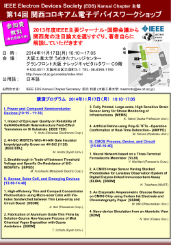


© Copyright 2026