
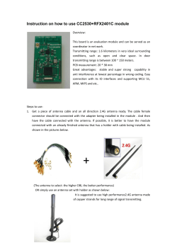
ANALYSIS OF DEFECTED GROUND
VOL. 10, NO. 2, FEBRUARY 2015
ARPN Journal of Engineering and Applied Sciences
ISSN 1819-6608
©2006-2015 Asian Research Publishing Network (ARPN). All rights reserved.
www.arpnjournals.com
ANALYSIS OF DEFECTED GROUND STRUCTURE NOTCHED
MONOPOLE ANTENNA
1
B T P Madhav, 1A Manikanta Prasanth, 1Sreeramineni Prasanth, 1Batchu Mohan Sai Krishna,
1
Devani Manikantha and 2Usirika Sharmila NagaSai
2Department
1
Department of ECE, K L University, Guntur DT, AP, India
of ECE, Sri Vasavi Institute of Engineering and Technology (SVIET), AP, India
E-Mail: [email protected]
ABSTRACT
A compact defected ground structure curved wideband monopole antenna and notched monopole antenna are
designed and presented in this paper. In the basic cured monopole antenna wide band characteristics are obtained and in the
case of notched monopole antenna, some frequency bands are cut- off in the wide band operation. The band notched
characteristic involved the WLAN operating band. The curved monopole antenna with defected ground structure is
operating in a wide bandwidth of 16 GHz. The designed antennas are showing impedance band width more than 140%
with VSWR less than 2 in the desired band.
Keywords: notch, wideband, monopole, defected ground structure (DGS), wireless local area network (WLAN).
1. INTRODUCTION
Design and development of microstrip antennas
[1] for different applications became the subject to the
antenna engineers all over the world. Demand of wideband
antennas with omnidirectional radiation patterns are
increasing day by day in the communication applications.
Over the Wide operating bands, some of the bands can be
rejected by using notched antennas. In order to notch
certain frequency bands, so many techniques and antennas
are available in the literature [2-6]. The conventional
methods including cutting a slot on the patch, inserting a
slit on the patch, using conductor backed plane, and
embedding a tuning stub within a slot on the patch or used
by the researchers in so many cases. Moreover band
rejection characteristics are generated by using a resonator
at the centre of antenna and with a pair of inverted Lshaped slots on the ground plane.
Moreover, many UWB applications require more
than one notch-band, necessitating the use of mutually
non-interacting band-notch elements. Different multiple
(dual, triple, quadruple) band-notched UWB antenna
topologies have also been reported in recent literature [710]. Use of split-ring resonators (SRRs) and
complementary split-ring resonators (CSRRs) to design
reconfigurable multiple band-notched UWB antennas have
been presented in [11-12].
In this paper a new design is proposed to get wide
band characteristics from one antenna and band notched
characteristics from another antenna. Comparing with the
conventional designs, the proposed models are occupying
a small size of 16 x 18 x 1.6 mm. Stable radiation patterns
at high frequencies and wide impedance band width are
achieved by designing the lower edges of the radiating
patch in the form of curved shape. In order to compensate
the effect of minimizing the size of antenna on the lowest
frequency, the radiating patch is notched by removing
square shaped slots at the bottom. The band stop
frequency can be controlled by adjusting the dimensions
of the filter structure at the lower side of the patch. A finite
element method based EM tool, HFSS is used to simulate
and optimize the models.
2. ANTENNA DIMENSIONAL CHARACTERISTICS
The geometry of the proposed models is shown in
Figure-1. Figure-1(a) shows the curved monopole antenna
operating in the wide band and Figure-1(b) shows notched
monopole antenna to reject the WLAN band. The width of
the microstrip feed line is kept constant to achieve 50 ohm
impedance in both the cases. A dielectric material of FR4
with dielectric constant 4.4 and loss tangent 0.02 is used in
the design of the models. The lower edge of the patch is
taken in the form of ark shaped step to generate additional
resonances with improved impedance bandwidth. The
notched band is generated with the vertical strip connected
to the rectangular ring embedded in the slot that is rotated
under the feeding line at the centre of the ground plane.
The notch frequency can be controlled by varying
the dimensions of the L1 and W1. The design equations
are constructed based on the resonant frequency and
dielectric material permittivity. fn is the centre rejected
frequency and it can be calculated from the following
equations.
(1)
(2)
(3)
The design values of the notched band antenna
parameters are Ws=16 mm, Ls=18 mm, width of the feed
line =1.9 mm, length of the feed line = 6 mm, defected
ground structure width W1= 3.4 mm, L1=3.8 mm, W2=0.4
mm and L2= 2 mm. Figure-1 shows the geometry of the
747
VOL. 10, NO. 2, FEBRUARY 2015
ARPN Journal of Engineering and Applied Sciences
ISSN 1819-6608
©2006-2015 Asian Research Publishing Network (ARPN). All rights reserved.
www.arpnjournals.com
notch band antenna with slotted defected ground structure.
Figure-2 shows the notch band antenna with the defected
ground structure i.e. planar quarter ground plane on the
bottom side. Figure-3 shows the wide band antenna
without notch and DGS on the bottom side.
Figure-3. Wideband Antenna with slotted defected ground
structure, (a) Top view, (b) Bottom view.
Figure-1. Notch Band Antenna with slotted defected
ground structure, (a) Top view, (b) Bottom view.
3. RESULTS AND ANALYSIS
Figure-4 shows the return loss curve for the
proposed three models. Notch band with slotted DGS is
resonating between 3.4 to 12 GHz with notch band
characteristics at 6.5 - 7.5 GHz. Wide band with DGS is
resonating between 4 GHz to 11 GHz with bandwidth of 7
GHz. Wide band antenna with slotted DGS is operating
between 4 to 20 GHz with bandwidth of 16 GHz.
Figure-5 shows the radiation pattern for notch
band antenna with slotted DGS in E and H plane. An
omnidirectional radiation pattern with cross polarization
less than -35 dB can be observed from the H plane.
Figure-6 shows the radiation pattern of wide band
antenna with DGS in E and H plane. Same kinds of results
are achieved in this case with low cross polarization
compared to notch band antenna with DGS. Figure-7
Figure-2. Wide Band Antenna with defected ground
structure, (a) Top view, (b) Bottom view.
Figure-4. Return loss Vs Frequency.
Figure-6 shows the radiation pattern of wide band
antenna with DGS in E and H plane. Same kinds of results
are achieved in this case with low cross polarization
compared to notch band antenna with DGS. Figure-7
748
VOL. 10, NO. 2, FEBRUARY 2015
ARPN Journal of Engineering and Applied Sciences
ISSN 1819-6608
©2006-2015 Asian Research Publishing Network (ARPN). All rights reserved.
www.arpnjournals.com
shows the quasi omni directional pattern in H plane for
wide band antenna with slotted DGS. In the E plane
nulling is observed at 70 degrees and 300 degrees.
Figure-5. Radiation pattern in H and E-plane for Notch Band Antenna with slotted DGS.
Figure-6. Radiation pattern in H and E-plane for Wide Band Antenna with DGS.
Figure-7. Radiation pattern in H and E-plane for Wide Band Antenna with slotted DGS.
749
VOL. 10, NO. 2, FEBRUARY 2015
ARPN Journal of Engineering and Applied Sciences
ISSN 1819-6608
©2006-2015 Asian Research Publishing Network (ARPN). All rights reserved.
www.arpnjournals.com
Figure-8. Frequency Vs Directivity of three models.
Figure-9. Frequency Vs Gain of three models.
Figure-10. Frequency Vs Efficiency of three models.
The directivity of the wide band antenna with
DGS at lower frequency band is somewhat better
compared to the other models. The notch band with slotted
DGS is giving better directivity at higher frequency band
compared to other models. The average gain obtained
from model 1 is 3 dB, model 2 is 2.8 dB and model 3 is
2.5 dB. The efficiency of model 1 is less than 70% at
750
VOL. 10, NO. 2, FEBRUARY 2015
ARPN Journal of Engineering and Applied Sciences
ISSN 1819-6608
©2006-2015 Asian Research Publishing Network (ARPN). All rights reserved.
www.arpnjournals.com
notch band and for wide band models it is above 80% in
the operating frequency range.
Figure-11 shows the impedance matching and
current distribution of the model 1. It is found that by
creating a step on the lower edges of the patch, the
impedance bandwidth is improved especially at the higher
frequencies. This occurred because the step affects the
electromagnetic coupling the patch and the ground plane.
Because of the existence of the discontinuity on the patch
and more flexibility of the surface current path compared
to the simple antenna, the higher resonant mode of the
antenna can be excited. As a result, a additional resonant
frequency appears that is tuneable by adjusting the
parameters of the step.
Figure-12 shows the current distribution of wide
band antenna with DGS. Figure-13 and Figure-14 are
showing the current distribution of wide band antenna
with slotted DGS at 7.1 and 13.5 GHz respectively. At
lower frequency the current distribution is maximum at
feed line and on the lower side of the radiating element. At
higher frequency the current distribution is all over the
surface of the radiating element including feed line.
Figure-13. Wide Band antenna with slotted DGS at 7.1
GHz.
Figure-14. Wide Band antenna with slotted DGS at
13.5 GHz.
Figure-11. Current distribution of Notch Band Antenna
with slotted DGS.
CONCLUSIONS
In this paper, we designed three antennas with
notch band character on one model and wide band
characteristics in other two models. Model 1 is giving a
band width of 8 GHz with notch band of 1 GHz at 6.5 7.5 GHz. Model 2 is providing the bandwidth of 7 GHz
and model 3 is providing the huge bandwidth 16 GHz.
Peak Directivity of 7 dB from model 1, 6 dB from model 2
and 5 dB from model 3 is attained. Peak gain of 5 dB, 4.5
dB and 3 dB is attained for model 1 to model 3. Efficiency
more than 80% achieved for wide band antennas whereas
efficiency less than 70% from model 1 at lower frequency
band. The proposed models can be used for ultra wideband
and Ku band communication systems.
ACKNOWLEDGEMENTS
Authors likes to express their gratitude towards
the Department of ECE and Management of K L
University for their support and encouragement during this
work.
Figure-12. Current distribution of Wide Band Antenna
with DGS.
REFERENCES
[1] B.T.P.Madhav,
Suraj
Chhatkuli,
A.
Manikantaprasanth, Y. Bhargav, U. Dinesh Naga
Venkata Sai and Syed Feeraz. 2014. Measurement of
Dimensional Characteristics of Microstrip Antenna
based on Mathematical Formulation. International
Journal of Applied Engineering Research. ISSN 09734562. 9(9): 1063-1074.
751
VOL. 10, NO. 2, FEBRUARY 2015
ARPN Journal of Engineering and Applied Sciences
ISSN 1819-6608
©2006-2015 Asian Research Publishing Network (ARPN). All rights reserved.
www.arpnjournals.com
[2] Vincenzo Lottici, Aldo D’Andrea and Umberto
Mengali. 2002. Channel Estimation for UltraWideband Communications. IEEE Journal on Selected
areas in Communications. 20(9): 1638-1645.
[3] B T P Madhav and K V V Kumar. 2014. Analysis of
CPW Fed Step Serrated Ultra Wide Band Antenna on
Rogers RT/Duroid Substrates. International Journal of
Applied Engineering Research. ISSN 0973-4562.
9(1): 53-58.
[4] B.T.P.Madhav, S. S. Mohan Reddy, Bandi Sanjay and
D.Ujwala. 2013. Trident Shaped Ultra Wideband
Antenna Analysis based on Substrate Permittivity.
International Journal of Applied Engineering
Research. ISSN 0973-4562. 8(12): 1355-1361.
with multiple notched bands based on etched slots on
the patch and/or split ring resonators on the feed line.
IEEE Trans. Antennas Propag. 56(9): 3063-3068.
[13] C. C. Lin and R. W. Ziolkowski. 2010. Tri-band
notched ultra-wideband antenna using capacitively
loaded loops (C LLs). In: Proc. IEEE Antennas
Propag. Soc. Int. Symp. pp. 1-4.
[14] C. C. Lin, P. Jin and R. W. Ziolkowski. 2012. Single,
dual and tri-band notched ultra wideband (UWB)
antennas using capacitively loaded loop (CLL)
resonators. IEEE Trans. Antennas Propag. 60(1): 102109.
[5] A. Mehdipour, K. Mohammadpour-Aghdam and R.
Faraji-Dana. 2007. Complete Dispersion Analysis of
Vivaldi Antenna for Ultra Wideband Applications.
Progress in Electromagnetics Research, PIER 77. pp.
85-96.
[6] B. T. P. Madhav, Sarat K. Kotamraju, P. Manikanta,
K. Narendra, M. R. Kishore and G. Kiran. 2014.
Tapered Step CPW-Fed Antenna for Wideband
Applications. ARPN Journal of Engineering and
Applied Sciences. ISSN 1819-6608. 9(10): 19671973.
[7] P. Lotfi, M. Azarmanesh and S. Soltani. 2013.
Rotatable dual band-notched UWB/triple-band
WLAN reconfigurable antenna. IEEE Antennas
Wireless Propag. Lett. 12: 104-107.
[8] Y. Sung. 2013. Triple band-notched UWB planar
monopole antenna using a modified H-shaped
resonator. IEEE Trans. Antennas Propag. 61(2): 953957.
[9] M. Ojaroudi, N. Ojaroudi and N. Ghadimi. 2013. Dual
band-notched small monopole antenna with novel
coupled inverted U-ring strip and novel fork-shaped
slit for UWB applications. IEEE Antennas Wireless
Propag. Lett. 12: 182-185.
[10] M. J. Almalkawi and V. K. Devabhaktuni. 2011. Quad
band-notched UWB antenna compatible with
WiMAX/INSAT/lower-upper WLAN applications.
Electron. Lett. 47(19): 1062-1063.
[11] M. Al-Husseini, J. C ostantine, C. G. C hristodoulou,
S. E. Barbin, A. El-Hajj and K. Y. Kabalan. 2012. A
reconfigurable frequency-notched UWB antenna with
split-ring resonators. In: Proc. Asia-Pacific Microw.
Conf. pp. 618-621.
[12] Y. Zhang, W. Hong, C. Yu, Z.-Q. Kuai, Y.-D. Don
and J.-Y. Zhou. 2008. Planar ultra wideband antennas
752


© Copyright 2026