
5.3 CardBus PC Card Electrical Specification
PC C ARD S TANDARD Volume 2 Electrical Specification REVISION HISTORY Date Electrical Specification Version PC Card Standard Release Revisions 11/90 1.0 PCMCIA 1.0 Memory only Interface 09/91 2.0 PCMCIA 2.0/JEIDA 4.1 Added I/O and Memory Interface Defined RESET signal Defined the WAIT# signal 11/92 2.01 PCMCIA 2.01 None 07/93 2.1 PCMCIA 2.1/JEIDA 4.2 Editorial corrections 02/95 5.0 February 1995 (5.0) Release Added CardBus PC Card Interface Redefined RFSH as VS1# Defined the RFU pin in the I/O-Memory interface as VS2# Defined multiple voltage operation Defined Multiple Function 16-bit PC Cards 03/95 5.01 March 1995 (5.01) Update Editorial corrections 05/95 5.02 May 1995 (5.02) Update Clarification of Power Waveforms at Power-on 11/95 5.1 November 1995 (5.1) Update Defined Custom Interfaces for PC Cards Defined Indirect Addressing for PC Cards Clarifications for Multifunction PC Cards 05/96 5.2 May 1996 (5.2) Update Defined Zoomed Video (ZV) Custom Interface 03/97 6.0 6.0 Release Defined Thermal Ratings for PC Cards 04/98 6.1 6.1 Update Defined Small PC Card form factor 02/99 7.0 7.0 Release Defined Digital Video Broadcasting (DVB) Custom Interface Defined PCI Power Management for CardBus PC Cards Defined PC Card Memory Paging Corrections to PCI Power Management for CardBus PC Cards 03/00 7.1 7.1 Update Defined OpenCable POD Custom Interface Noted July 1, 2000 removal of references to DMA (Direct Memory Access) Modification of CardBus Clock Control Protocol 11/00 7.2 7.2 Update Added maximum current requirements to 16-bit PC Card interface Removed all references to Direct Memory Access (DMA) 04/01 8.0 8.0 Release Added CardBay PC Card Interface Added Vcore Supplemental Voltage Redefined VPP1 and VPP2 as VPP ©2001 PCMCIA/JEITA All rights reserved. No part of this publication may be reproduced, stored in a retrieval system, or transmitted, in any form or by any means, mechanical, electronic, photocopying, recording or otherwise, without prior written permission of PCMCIA and JEITA. Published in the United States of America. ELECTRICAL SPECIFICATION CONTENTS 1. Overview _____________________________________________ 1 1.1 Summary of Electrical Specification Changes...........................................................................1 1.1.1 PCMCIA 2.0/JEIDA 4.1 (September 1991)...................................................................................................... 1 1.1.2 PCMCIA 2.1/JEIDA 4.2 (July 1993) ................................................................................................................. 1 1.1.3 PC Card Standard February 1995 Release (Release 5.0) ............................................................................... 1 1.1.4 PC Card Standard March 1995 Update (Release 5.01) .................................................................................. 2 1.1.5 PC Card Standard May 1995 Update (Release 5.02)...................................................................................... 2 1.1.6 PC Card Standard November 1995 Update (Release 5.1) ............................................................................. 2 1.1.7 PC Card Standard May 1996 Update (Release 5.2)........................................................................................ 2 1.1.8 PC Card Standard 6.0 Release (March 1997) .................................................................................................. 2 1.1.9 PC Card Standard 6.1 Release (April 1998) .................................................................................................... 2 1.1.10 PC Card Standard 7.0 Release (February 1999).............................................................................................. 2 1.1.11 PC Card Standard 7.1 Update (March 2000) .................................................................................................. 3 1.1.12 PC Card Standard 7.2 Update (November 2000) ........................................................................................... 3 1.1.13 PC Card Standard Release 8.0 (April 2001) .................................................................................................... 3 1.2 Conventions ...................................................................................................................................3 1.2.1 Signal Naming .................................................................................................................................................... 3 1.2.2 Numeric Representation.................................................................................................................................... 3 1.2.3 Bit Action Representation ................................................................................................................................. 4 1.2.4 Signal Summary ................................................................................................................................................. 4 2. Common Pin Description _______________________________ 5 2.1 Power and Ground Pins ...............................................................................................................5 2.1.1 VCC and GND Pins............................................................................................................................................. 5 2.1.2 VPP/VCORE Pins.................................................................................................................................................. 5 2.1.3 Power (Thermal) Considerations ..................................................................................................................... 6 2.2 Interface Configuration Pins........................................................................................................6 2.2.1 Card Detect Pins (CD[2::1]# and CCD[2::1]#) ................................................................................................ 6 2.2.2 Voltage Sense Pins (VS[2::1]# and CVS[2::1]) ................................................................................................. 7 3. Card Type Detection Mechanism ________________________ 9 3.1 PC Card Encodings .......................................................................................................................9 3.2 Socket Key Selection ...................................................................................................................10 3.3 Graceful Rejection in 16–bit PC Card Only Sockets ...............................................................11 3.4 Determining Card Type in CardBus PC Card Capable Sockets...........................................11 3.5 Determining Card Type in CardBay PC Card Capable Sockets...........................................12 4. 16-bit PC Card Electrical Interface ______________________ 13 ©2001 PCMCIA/JEITA iii OVERVIEW 4.1 Compatibility Issues....................................................................................................................13 4.1.1 RESET and WAIT# Support ........................................................................................................................... 13 4.1.2 VS1# replaces RFSH (pin 43) .......................................................................................................................... 13 4.2 Pin Assignments..........................................................................................................................13 4.3 16-bit PC Card Features..............................................................................................................16 4.3.1 Memory Address Space .................................................................................................................................. 16 4.3.2 Memory Only Interface ................................................................................................................................... 17 4.3.3 I/O Address Space........................................................................................................................................... 17 4.3.4 I/O Interface ..................................................................................................................................................... 18 4.3.5 Custom Interfaces ............................................................................................................................................ 18 4.3.6 Configurable Cards.......................................................................................................................................... 19 4.4 Signal Description .......................................................................................................................19 4.4.1 Address BUS (A[25::0]).................................................................................................................................... 19 4.4.2 Data BUS (D[15::0]) .......................................................................................................................................... 19 4.4.3 Card Enable (CE[2::1]#)................................................................................................................................... 19 4.4.4 Output Enable (OE#) ....................................................................................................................................... 20 4.4.5 Write Enable (WE#) ......................................................................................................................................... 20 4.4.6 Ready (READY)................................................................................................................................................ 20 4.4.7 Interrupt Request (IREQ#) [I/O and Memory Interface] ........................................................................... 21 4.4.7.1 Interrupt Request Routing .................................................................................................................. 21 4.4.7.2 Level and Pulsed Mode Interrupt Support....................................................................................... 22 4.4.7.2.1 Level Mode Interrupt Signal....................................................................................................... 22 4.4.7.2.2 Pulsed Mode Interrupt Signal..................................................................................................... 22 4.4.8 Card Detect (CD[2::1]#)................................................................................................................................... 23 4.4.9 Write Protect (WP) [Memory Only Interface] .............................................................................................. 23 4.4.10 I/O Is 16 Bit Port (IOIS16#) [I/O and Memory Interface].......................................................................... 23 4.4.11 Attribute Memory Select (REG#) ................................................................................................................... 23 4.4.12 Battery Voltage Detect (BVD[2::1]) [Memory Only Interface].................................................................... 24 4.4.13 Status Changed (STSCHG#) [I/O and Memory Interface]......................................................................... 24 4.4.14 Audio Digital Waveform (SPKR#) [I/O and Memory Interface] .............................................................. 24 4.4.15 Program and Peripheral Voltages (VPP) ....................................................................................................... 25 4.4.16 Voltage and Ground (VCC & GND) ............................................................................................................... 25 4.4.16.1 Socket VCC for CIS Read...................................................................................................................... 25 4.4.16.2 PC Card VCC for CIS Read .................................................................................................................. 26 4.4.16.3 Changing PC Card VCC ....................................................................................................................... 26 4.4.17 Voltage Sense (VS[2::1]#) ................................................................................................................................ 26 4.4.18 I/O Read (IORD#) [I/O and Memory Interface]......................................................................................... 27 4.4.19 I/O Write (IOWR#) [I/O and Memory Interface] ....................................................................................... 27 4.4.20 Card Reset (RESET) ......................................................................................................................................... 28 4.4.21 Extend Bus Cycle (WAIT#)............................................................................................................................. 28 4.4.22 Input Port Acknowledge (INPACK#) [I/O and Memory Interface]......................................................... 28 4.5 Memory Function ........................................................................................................................28 4.5.1 Common Memory Function ........................................................................................................................... 28 iv ©2001 PCMCIA/JEITA ELECTRICAL SPECIFICATION 4.5.1.1 Common Memory Read Function for PC Cards .............................................................................. 28 4.5.1.2 Common Memory Write Function for PC Cards ............................................................................. 29 4.5.1.3 Common Memory Write Function for OTPROM, EPROM and Flash Memory .......................... 29 4.5.2 Attribute Memory Function............................................................................................................................ 30 4.5.2.1 Attribute Memory Read Function ...................................................................................................... 30 4.5.2.2 Attribute Memory Write Function ..................................................................................................... 30 4.5.2.3 Attribute Memory Write Function for Dual Supply OTPROM, EPROM and Flash Memory ... 30 4.5.3 Write Protect Function..................................................................................................................................... 31 4.6 Timing Functions.........................................................................................................................31 4.6.1 Common Memory Read Timing .................................................................................................................... 31 4.6.2 Common and Attribute Memory Write Timing........................................................................................... 33 4.6.2.1 Common Memory Write Timing........................................................................................................ 34 4.6.3 Attribute Memory Read Timing Specification ............................................................................................. 34 4.6.4 Attribute Memory Write Timing Specification ............................................................................................ 34 4.6.5 Memory Timing Diagrams ............................................................................................................................. 35 4.7 Electrical Interface .......................................................................................................................36 4.7.1 Signal Interface ................................................................................................................................................. 36 4.7.2 Memory Address Decoding............................................................................................................................ 38 4.7.2.1 Function Configuration Registers Address Decoding..................................................................... 39 4.7.3 I/O Address Space Decoding......................................................................................................................... 39 4.7.3.1 Independent I/O Address Window .................................................................................................. 39 4.7.3.2 Overlapping I/O Address Window .................................................................................................. 40 4.8 Card Detect...................................................................................................................................41 4.9 Battery Voltage Detect ................................................................................................................41 4.10 Power-up and Power-down ...................................................................................................42 4.10.1 Power-up/Power-down Timing .................................................................................................................... 42 4.10.2 Average Current During Card Configuration.............................................................................................. 43 4.10.3 Data Retention .................................................................................................................................................. 44 4.10.4 Supplement ....................................................................................................................................................... 44 4.11 I/O Function .............................................................................................................................44 4.11.1 I/O Transfer Function ..................................................................................................................................... 44 4.11.2 I/O Input Function for I/O Cards ................................................................................................................. 44 4.11.3 I/O Output Function for I/O Cards .............................................................................................................. 45 4.11.4 I/O Read (Input) Timing Specification ......................................................................................................... 46 4.11.5 I/O Write (Output) Timing Specification ..................................................................................................... 48 4.12 Function Configuration...........................................................................................................49 4.12.1 Overview ........................................................................................................................................................... 49 4.12.2 Single Function PC Cards ............................................................................................................................... 49 4.12.3 Multiple Function PC Cards ........................................................................................................................... 49 4.12.4 Function Configuration Registers (FCRs) ..................................................................................................... 50 4.13 Card Configuration..................................................................................................................51 4.13.1 Configuration Option Register ....................................................................................................................... 52 ©2001 PCMCIA/JEITA v OVERVIEW 4.13.2 Configuration and Status Register................................................................................................................. 55 4.13.3 Pin Replacement Register ............................................................................................................................... 56 4.13.4 Socket and Copy Register ............................................................................................................................... 57 4.13.5 Extended Status Register................................................................................................................................. 58 4.13.6 I/O Base Registers (0 .. 3)................................................................................................................................ 58 4.13.7 I/O Limit Register............................................................................................................................................ 59 4.13.8 Power Management Support Register .......................................................................................................... 59 4.13.9 Address Extension Registers .......................................................................................................................... 61 4.14 Indirect Access to PC Card Memory .....................................................................................63 5. CardBus PC Card Electrical Interface ___________________ 65 5.1 CardBus PC Card Signal Description.......................................................................................65 5.1.1 Pin Assignments............................................................................................................................................... 66 5.1.2 Signal/Pin Description.................................................................................................................................... 70 5.1.2.1 System Pins ........................................................................................................................................... 70 5.1.2.2 Address and Data Pins ........................................................................................................................ 70 5.1.2.3 Interface Control Pins .......................................................................................................................... 71 5.1.2.4 Arbitration Pins (Bus Masters Only) ................................................................................................. 71 5.1.2.5 Error Reporting Pins ............................................................................................................................ 72 5.1.2.6 Interrupt Request Pin........................................................................................................................... 72 5.1.2.7 Additional Signals................................................................................................................................ 72 5.1.3 Central Resource Functions ............................................................................................................................ 73 5.2 CardBus PC Card Operation .....................................................................................................73 5.2.1 Bus Commands ................................................................................................................................................ 73 5.2.1.1 Command Definition ........................................................................................................................... 73 5.2.1.2 Command Usage Rules ....................................................................................................................... 75 5.2.2 CardBus PC Card Protocol Fundamentals ................................................................................................... 76 5.2.2.1 Basic Transfer Control ......................................................................................................................... 77 5.2.2.2 Addressing ............................................................................................................................................ 77 5.2.2.3 Byte Alignment..................................................................................................................................... 79 5.2.2.4 Bus Driving and Turnaround ............................................................................................................. 79 5.2.3 Bus Transactions .............................................................................................................................................. 80 5.2.3.1 Read Transaction.................................................................................................................................. 80 5.2.3.2 Write Transaction................................................................................................................................. 82 5.2.3.3 Transaction Termination ..................................................................................................................... 82 5.2.3.3.1 Master Initiated Termination...................................................................................................... 83 5.2.3.3.2 Target Initiated Termination....................................................................................................... 85 5.2.4 Arbitration......................................................................................................................................................... 89 5.2.5 Arbitration Signaling Protocol ....................................................................................................................... 89 5.2.5.1 Fast Back-to-Back Transactions .......................................................................................................... 91 5.2.5.2 CardBus PC Card Idle Condition....................................................................................................... 93 5.2.5.3 Latency................................................................................................................................................... 93 5.2.5.3.1 Managing Latency on CardBus PC Card .................................................................................. 94 5.2.5.3.2 Low Latency Design Guidelines ................................................................................................ 95 vi ©2001 PCMCIA/JEITA ELECTRICAL SPECIFICATION 5.2.6 Exclusive Access ............................................................................................................................................... 95 5.2.6.1 Starting an Exclusive Access ............................................................................................................... 98 5.2.6.2 Continuing an Exclusive Access......................................................................................................... 99 5.2.6.3 Accessing a Locked Agent................................................................................................................... 99 5.2.6.4 Completing an Exclusive Access ...................................................................................................... 100 5.2.6.5 Supporting CBLOCK# and Write-back Cache Coherency ........................................................... 100 5.2.6.6 Complete Bus Lock............................................................................................................................. 101 5.2.7 Other Bus Operations .................................................................................................................................... 101 5.2.7.1 Device Selection .................................................................................................................................. 101 5.2.7.2 Special Cycle ....................................................................................................................................... 102 5.2.7.3 Address/Data Stepping..................................................................................................................... 103 5.2.7.4 Configuration Cycle ........................................................................................................................... 104 5.2.7.4.1 Generating Configuration Cycles............................................................................................. 106 5.2.7.4.1.1 Configuration Mechanism............................................................................................... 106 5.2.7.4.1.2 Generating Special Cycles with the Configuration Mechanism................................. 108 5.2.8 Error Functions............................................................................................................................................... 108 5.2.8.1 Parity .................................................................................................................................................... 108 5.2.8.2 Error Reporting................................................................................................................................... 110 5.2.8.2.1 Parity Error Response and Reporting on CPERR# ................................................................ 110 5.2.8.2.2 Error Response and Reporting on CSERR# ............................................................................ 111 5.2.9 Cache Support................................................................................................................................................. 112 5.2.10 Clock Control .................................................................................................................................................. 114 5.2.10.1 Clock Frequency ................................................................................................................................. 114 5.2.10.2 Clock Control Protocol....................................................................................................................... 114 5.2.10.2.1 Clock Stop or Slow down ...................................................................................................... 115 5.2.10.2.2 Clock Restart or Speed up ..................................................................................................... 116 5.2.10.2.3 Maintaining the Interface Clock ........................................................................................... 117 5.2.11 Status Changed Notification......................................................................................................................... 118 5.2.11.1 Card Status Changed ......................................................................................................................... 118 5.2.11.2 System and Interface Wake up ......................................................................................................... 118 5.2.11.3 Register Descriptions ......................................................................................................................... 120 5.2.11.3.1 Function Event Register......................................................................................................... 120 5.2.11.3.2 Function Event Mask Register .............................................................................................. 122 5.2.11.3.3 Function Present State Register ............................................................................................ 124 5.2.11.3.4 Force Event Capability........................................................................................................... 125 5.2.11.3.5 Default Field Values............................................................................................................... 127 5.2.12 Card Audio ..................................................................................................................................................... 127 5.2.13 Special Design Considerations ..................................................................................................................... 128 5.2.13.1 Multiple Retry Termination .............................................................................................................. 128 5.3 CardBus PC Card Electrical Specification .............................................................................128 5.3.1 Overview ......................................................................................................................................................... 128 5.3.1.1 Dynamic vs. Static Drive Specification ............................................................................................ 129 5.3.2 Component Specifications............................................................................................................................. 129 5.3.2.1 3.3 V Signaling Environment ............................................................................................................ 130 ©2001 PCMCIA/JEITA vii OVERVIEW 5.3.2.1.1 DC Specifications........................................................................................................................ 130 5.3.2.1.2 AC Specifications........................................................................................................................ 131 5.3.2.1.3 CSTSCHG Buffer Specification................................................................................................. 131 5.3.2.1.4 CCLK AC Specifications............................................................................................................ 131 5.3.2.1.5 Maximum AC Ratings and Device Protection (CCLK) ......................................................... 132 5.3.2.1.6 Noise Considerations................................................................................................................. 133 5.3.2.2 Timing Specification .......................................................................................................................... 134 5.3.2.2.1 Clock Specifications ................................................................................................................... 134 5.3.2.2.2 Timing Parameters ..................................................................................................................... 135 5.3.2.2.3 Measurement and Test Conditions .......................................................................................... 136 5.3.2.3 Vendor Provided Specifications ....................................................................................................... 137 5.3.3 System (Motherboard) Specifications.......................................................................................................... 137 5.3.3.1 Clock Skew.......................................................................................................................................... 137 5.3.3.2 Reset ..................................................................................................................................................... 138 5.3.3.3 Pull-ups................................................................................................................................................ 139 5.3.3.3.1 Pull-up Values for Control Signals .......................................................................................... 140 5.3.3.3.2 Pull-up Values for Card Detect and Voltage Sense Pins....................................................... 140 5.3.3.3.3 Pull-up Resistor Requirements ................................................................................................. 141 5.3.3.4 Power Sequencing.............................................................................................................................. 144 5.3.3.5 System Timing Budget ...................................................................................................................... 144 5.3.3.6 Physical Requirements ...................................................................................................................... 144 5.3.3.6.1 Routing and Layout of Four Layer Boards ............................................................................. 144 5.3.3.6.2 Motherboard Impedance........................................................................................................... 144 5.3.4 CardBus PC Card Specifications .................................................................................................................. 145 5.3.4.1 Power Requirements.......................................................................................................................... 145 5.3.4.1.1 Decoupling .................................................................................................................................. 145 5.3.4.1.2 External Power Supplies ........................................................................................................... 145 5.3.4.2 Physical Requirements ...................................................................................................................... 145 5.3.4.2.1 Trace Length Limits ................................................................................................................... 145 5.3.4.2.2 Impedance ................................................................................................................................... 145 5.3.4.2.3 Signal Loading............................................................................................................................ 146 5.4 CardBus PC Card Programming Model ................................................................................146 5.4.1 Overview......................................................................................................................................................... 146 5.4.2 Card Organization ......................................................................................................................................... 146 5.4.2.1 Configuration Space........................................................................................................................... 151 5.4.2.1.1 Command.................................................................................................................................... 154 5.4.2.1.2 Status............................................................................................................................................ 155 5.4.2.1.3 Cache Line size ........................................................................................................................... 157 5.4.2.1.4 Latency Timer ............................................................................................................................. 157 5.4.2.1.5 Header Type................................................................................................................................ 158 5.4.2.1.6 Built-in Self Test (BIST).............................................................................................................. 158 5.4.2.1.7 Base Address Register ............................................................................................................... 158 5.4.2.1.8 CIS Pointer................................................................................................................................... 160 5.4.2.1.9 Expansion ROM Base Address Register ................................................................................. 162 viii ©2001 PCMCIA/JEITA ELECTRICAL SPECIFICATION 5.4.2.1.10 Cap_Ptr .................................................................................................................................... 162 5.4.2.1.11 Interrupt Pin ............................................................................................................................ 162 5.4.2.1.12 Tuple Space ............................................................................................................................. 163 5.4.2.1.13 Register Summary .................................................................................................................. 163 5.4.2.2 Memory Space .................................................................................................................................... 164 5.4.2.3 I/O Space............................................................................................................................................. 165 5.4.2.4 Expansion ROM.................................................................................................................................. 165 5.5 Requirements For CardBus PC Cards and Sockets ..............................................................167 5.5.1 Overview ......................................................................................................................................................... 167 5.5.2 Software Requirements ................................................................................................................................. 167 5.5.2.1 Socket Services .................................................................................................................................... 167 5.5.2.2 Card Services....................................................................................................................................... 168 5.5.2.3 System Resource Availability ........................................................................................................... 168 5.5.2.4 System Resource Determination....................................................................................................... 168 5.5.2.5 Enabler Support.................................................................................................................................. 169 5.5.3 Card Requirements ........................................................................................................................................ 169 5.5.3.1 Configuration Space........................................................................................................................... 169 5.5.3.2 Required CIS ....................................................................................................................................... 169 5.5.3.3 Required Signals................................................................................................................................. 170 5.5.3.4 Pull-up/Pull-down Resistors............................................................................................................ 170 5.5.3.5 CSTSCHG Support ............................................................................................................................. 170 5.5.3.6 Power Consumption .......................................................................................................................... 171 5.5.3.7 I/O Space Support.............................................................................................................................. 171 5.5.4 Socket Requirements...................................................................................................................................... 171 5.5.4.1 16-bit PC Card Support...................................................................................................................... 171 5.5.4.2 Address Spaces ................................................................................................................................... 172 5.5.4.2.1 Memory Space............................................................................................................................. 172 5.5.4.2.2 I/O Support................................................................................................................................. 173 5.5.4.2.2.1 CardBus PC Card with Memory Mapped I/O............................................................. 173 5.5.4.2.2.2 CardBus PC Card with I/O Space.................................................................................. 173 5.5.4.2.2.3 ISA Support Implications ................................................................................................ 174 5.5.4.3 Interrupt Handling and Routing ...................................................................................................... 174 5.5.4.3.1 Functional Interrupts (CINT#).................................................................................................. 174 5.5.4.3.2 Status Change Events................................................................................................................. 174 5.5.4.4 Register Descriptions ......................................................................................................................... 175 5.5.4.4.1 Socket EVENT Register.............................................................................................................. 175 5.5.4.4.2 Socket MASK Register ............................................................................................................... 176 5.5.4.4.3 Socket PRESENT STATE Register ............................................................................................ 177 5.5.4.4.4 FORCE Event Capability ........................................................................................................... 180 5.5.4.4.5 CONTROL Register.................................................................................................................... 182 5.5.4.5 VPP/VCORE Power Requirements..................................................................................................... 182 5.5.4.6 Card Insertion and Removal............................................................................................................. 183 5.5.4.6.1 Card Insertion ............................................................................................................................. 183 5.5.4.6.2 Card Removal ............................................................................................................................. 184 ©2001 PCMCIA/JEITA ix OVERVIEW 5.5.4.7 Power Cycling the Interface.............................................................................................................. 185 5.5.4.7.1 Signal Requirements .................................................................................................................. 185 5.5.4.7.2 CSTSCHG Requirements........................................................................................................... 185 5.5.4.7.3 In-Rush Current.......................................................................................................................... 185 5.5.4.8 Required Pins...................................................................................................................................... 186 5.5.4.9 Clock Stopping Support .................................................................................................................... 186 5.5.4.10 Special Cycle Support ........................................................................................................................ 186 5.5.4.11 Actions When Adapter Is Reset........................................................................................................ 186 6. PCI Bus Power Management Interface for CardBus Cards 187 6.1 Introduction................................................................................................................................187 6.1.1 Goals of this Specification ............................................................................................................................. 187 6.1.2 Target Audience ............................................................................................................................................. 188 6.1.3 Overview/Scope ............................................................................................................................................ 188 6.1.4 Glossary of Terms .......................................................................................................................................... 190 6.1.5 Related Documents ........................................................................................................................................ 191 6.1.6 Conventions Used in this Chapter............................................................................................................... 192 6.2 CardBus Power Management Overview ...............................................................................192 6.2.1 CardBus Power Management States ........................................................................................................... 192 6.2.1.1 CardBus Function Power States ....................................................................................................... 192 6.2.1.2 Bus Power States ................................................................................................................................ 193 6.2.1.3 Device-Class Specifications............................................................................................................... 193 6.2.1.4 Bus Support for CardBus Function Power Management ............................................................. 194 6.3 CardBus Power Management Interface .................................................................................195 6.3.1 Capabilities List Data Structure ................................................................................................................... 196 6.3.1.1 Capabilities List Cap_Ptr Location .................................................................................................. 197 6.3.2 Power Management Register Block Definition .......................................................................................... 198 6.3.2.1 Capability Identifier - Cap_ID (Offset = 0) ..................................................................................... 198 6.3.2.2 Next Item Pointer - Next_Item_Ptr (Offset = 1).............................................................................. 199 6.3.2.3 PMC - Power Management Capabilities (Offset = 2) .................................................................... 199 6.3.2.4 PMCSR - Power Management Control/Status (Offset = 4) .......................................................... 200 6.3.2.5 PMCSR_BSE - PMCSR PCI-to-PCI Bridge Support Extensions (Offset=6) – Not Used in CardBus Cards - Reserved .................................................................................................................... 202 6.3.2.6 Data (Offset = 7) ................................................................................................................................. 203 6.4 CardBus Bus Power States .......................................................................................................205 6.4.1 CardBus B0 State - Fully On ......................................................................................................................... 205 6.4.2 CardBus B1 State ............................................................................................................................................ 206 6.4.3 CardBus B2 State ............................................................................................................................................ 206 6.4.4 CardBus B3 State - Off ................................................................................................................................... 206 6.4.5 CardBus Bus Power State Transitions ......................................................................................................... 207 6.4.6 CardBus Clocking Considerations............................................................................................................... 207 6.4.7 Control/Status of CardBus Bus Power Management States .................................................................... 208 6.4.7.1 Control of Secondary Bus Power Source and Clock...................................................................... 208 x ©2001 PCMCIA/JEITA ELECTRICAL SPECIFICATION 6.5 CardBus Function Power Management States......................................................................209 6.5.1 CardBus Function D0 State ........................................................................................................................... 209 6.5.2 CardBus Function D1 State ........................................................................................................................... 210 6.5.3 CardBus Function D2 State ........................................................................................................................... 210 6.5.4 CardBus Function D3 State ........................................................................................................................... 210 6.5.4.1 Software Accessible D3 (D3hot) ......................................................................................................... 211 6.5.4.2 Power Off (D3cold)............................................................................................................................... 211 6.5.5 CardBus Function Power State Transitions ................................................................................................ 211 6.5.6 CardBus Card Function Power Management Policies .............................................................................. 213 6.5.6.1 State Transition Recovery Time Requirements .............................................................................. 217 6.6 CardBus Cards and Power Management ..............................................................................218 6.6.1 CardBus Card Context................................................................................................................................... 221 6.6.2 PME_En/PME_Status and CardBus Cards ................................................................................................ 222 6.7 Power Management Events .....................................................................................................223 6.7.1 Auxiliary Power for D3cold Power Management Events ........................................................................... 223 6.8 Software Support for PCI Power Management ....................................................................224 6.8.1 Identifying CardBus Function Capabilities ................................................................................................ 224 6.8.2 Placing CardBus Functions in a Low Power State..................................................................................... 225 6.8.2.1 Buses..................................................................................................................................................... 225 6.8.2.2 D3 State ................................................................................................................................................ 225 6.8.3 Restoring PCI Functions From a Low Power State.................................................................................... 225 6.8.3.1 Dx States and the DSI Bit................................................................................................................... 225 6.8.3.2 D1 and D2 States................................................................................................................................. 225 6.8.3.3 D3 State ................................................................................................................................................ 226 6.8.4 Wake Events.................................................................................................................................................... 226 6.8.4.1 Wake Event Support .......................................................................................................................... 226 6.8.4.2 The D0 "Initialized" State From a Wake Event ............................................................................... 226 6.8.5 Get Capabilities .............................................................................................................................................. 227 6.8.6 Set Power State ............................................................................................................................................... 227 6.8.7 Get Power Status ............................................................................................................................................ 227 6.9 Other Considerations................................................................................................................227 PC Card Interface __________________________ 229 7. CardBay 7.1 CardBay PC Card Electrical Interface ....................................................................................229 7.1.1 Detecting the CardBay PC Card................................................................................................................... 229 7.1.2 Determining CardBay Card Functionality.................................................................................................. 229 7.1.2.1 Query Pin Requirements and Characteristics................................................................................. 230 7.2 CardBay PC Card Physical Interface ......................................................................................232 7.2.1 Pin Assignment............................................................................................................................................... 234 8. Special Cycle Messages_______________________________ 237 8.1 Message Encodings ...................................................................................................................237 ©2001 PCMCIA/JEITA xi OVERVIEW 8.2 Use of Specific Encodings ........................................................................................................237 9. CardBus PC Card Connector Test Methodology _________ 239 9.1 Background ................................................................................................................................239 9.2 Test Hardware Recommendations .........................................................................................239 9.2.1 General Recommendations........................................................................................................................... 239 9.2.2 Host-side Requirements ................................................................................................................................ 240 9.2.3 Card-side Recommendations ....................................................................................................................... 240 9.2.4 Measurement Equipment Recommendations ............................................................................................ 240 9.3 Test Board Considerations .......................................................................................................240 9.3.1 Host-side Implementation ............................................................................................................................ 241 9.3.2 Card-side Implementation............................................................................................................................ 242 9.4 Measurement Methodology.....................................................................................................243 9.4.1 Finding the Worst Case Ground Bounce .................................................................................................... 243 10. PC Card Custom Interfaces _________________________ 245 10.1 Custom Interface Requirements...........................................................................................245 10.1.1 Purpose/Overview ........................................................................................................................................ 245 10.1.2 Compatibility.................................................................................................................................................. 245 10.1.3 Pin Assignments............................................................................................................................................. 245 10.1.4 Features ........................................................................................................................................................... 245 10.1.5 Signal Description .......................................................................................................................................... 245 10.1.6 Functions ......................................................................................................................................................... 246 10.1.7 Timing ............................................................................................................................................................. 246 10.1.8 Electrical Interface.......................................................................................................................................... 246 10.1.9 Specific Signals and Functions ..................................................................................................................... 246 10.2 ZV Port Custom Interface (0141H).......................................................................................247 10.2.1 Overview......................................................................................................................................................... 247 10.2.2 Compatibility.................................................................................................................................................. 247 10.2.3 Pin Assignments............................................................................................................................................. 249 10.2.4 Features ........................................................................................................................................................... 251 10.2.5 Signal Description .......................................................................................................................................... 251 10.2.5.1 PCLK .................................................................................................................................................... 251 10.2.5.2 VSYNC................................................................................................................................................. 251 10.2.5.3 HREF.................................................................................................................................................... 251 10.2.5.4 Y[7::0] ................................................................................................................................................... 251 10.2.5.5 UV[7::0]................................................................................................................................................ 251 10.2.5.6 LRCLK ................................................................................................................................................. 251 10.2.5.7 SDATA................................................................................................................................................. 252 10.2.5.8 SCLK .................................................................................................................................................... 252 10.2.5.9 MCLK................................................................................................................................................... 252 10.2.6 Functions ......................................................................................................................................................... 253 xii ©2001 PCMCIA/JEITA ELECTRICAL SPECIFICATION 10.2.7 Timing.............................................................................................................................................................. 253 10.2.7.1 Video Interface Timing ...................................................................................................................... 253 10.2.7.2 Audio Interface Timing ..................................................................................................................... 254 10.2.8 Electrical Interface .......................................................................................................................................... 254 10.2.9 Specific Signals and Functions ..................................................................................................................... 255 10.2.10 PC Card Connector Test Methodology ................................................................................................... 255 10.3 DVB CI Port Custom Interface (0241h) ...............................................................................257 10.3.1 Overview ......................................................................................................................................................... 257 10.3.2 Compatibility .................................................................................................................................................. 258 10.3.3 Pin Assignments............................................................................................................................................. 259 10.3.4 Features............................................................................................................................................................ 260 10.3.5 Signal Description .......................................................................................................................................... 261 10.3.5.1 MDI[7::0].............................................................................................................................................. 261 10.3.5.2 MISTRT ................................................................................................................................................ 261 10.3.5.3 MIVAL ................................................................................................................................................. 261 10.3.5.4 MDO[7::0] ............................................................................................................................................ 261 10.3.5.5 MOSTRT .............................................................................................................................................. 261 10.3.5.6 MOVAL ............................................................................................................................................... 261 10.3.5.7 MCLKI ................................................................................................................................................. 261 10.3.5.8 MCLKO................................................................................................................................................ 261 10.3.6 Functions ......................................................................................................................................................... 262 10.3.7 Timing.............................................................................................................................................................. 262 10.3.8 Electrical Interface .......................................................................................................................................... 264 10.3.9 Specific Signals and Functions ..................................................................................................................... 264 10.4 OpenCable POD Port Custom Interface (0341h) ...........................................................265 10.4.1 Overview ......................................................................................................................................................... 265 Compatibility .............................................................................................................................................................. 266 10.4.3 Pin Assignments............................................................................................................................................. 267 10.4.4 Features............................................................................................................................................................ 269 10.4.5 Signal Description .......................................................................................................................................... 270 10.4.5.1 MDI[7::0].............................................................................................................................................. 270 10.4.5.2 MISTRT ................................................................................................................................................ 270 10.4.5.3 MIVAL ................................................................................................................................................. 270 10.4.5.4 MDO[7::0] ............................................................................................................................................ 270 10.4.5.5 MOSTRT .............................................................................................................................................. 270 10.4.5.6 MOVAL ............................................................................................................................................... 270 10.4.5.7 MCLKI ................................................................................................................................................. 270 10.4.5.8 MCLKO................................................................................................................................................ 270 10.4.5.9 EXTCH# (Extended Channel)........................................................................................................... 271 10.4.5.10 DRX .................................................................................................................................................. 271 10.4.5.11 ETX ................................................................................................................................................... 271 10.4.5.12 CRX................................................................................................................................................... 271 10.4.5.13 CTX................................................................................................................................................... 271 10.4.5.14 ITX .................................................................................................................................................... 271 ©2001 PCMCIA/JEITA xiii OVERVIEW 10.4.5.15 QTX .................................................................................................................................................. 271 10.4.6 Functions ......................................................................................................................................................... 271 10.4.7 Timing ............................................................................................................................................................. 272 10.4.7.1 Transport Stream Interface Timing.................................................................................................. 272 10.4.8 Electrical Interface.......................................................................................................................................... 274 10.4.9 Specific Signals and Functions ..................................................................................................................... 274 xiv ©2001 PCMCIA/JEITA ELECTRICAL SPECIFICATION FIGURES Figure 3–1 CCD[2::1]# and CVS[2::1] Connections ................................................................12 Figure 4-1: Recommended PC Compatible Interrupt Request Signals................................22 Figure 4-2: Read Timing Diagram.............................................................................................35 Figure 4-3: Write Timing Diagram............................................................................................36 Figure 4-4: Card Detect ...............................................................................................................41 Figure 4-5: Power-Up/Down Timing.......................................................................................43 Figure 4-6: Power-Down/Power-Up Timing When Changing Vcc ....................................43 Figure 4-7: I/O Read Timing .....................................................................................................46 Figure 4-8: I/O Write Timing ....................................................................................................48 Figure 5-1 CardBus PC Card Basic Read Operation...............................................................81 Figure 5-2 CardBus PC Card Basic Write Operation..............................................................82 Figure 5-3 CardBus PC Card Master Initiated Termination .................................................83 Figure 5-4 CardBus PC Card Master-abort Termination.......................................................85 Figure 5-5 Target Initiated Termination...................................................................................88 Figure 5-6 CardBus PC Card Basic Arbitration.......................................................................90 Figure 5-7 Arbitration for Back-to-Back Access ......................................................................93 Figure 5-8 Components of Access Latency..............................................................................94 Figure 5-9 CardBus PC Card Starting an Exclusive Access ..................................................98 Figure 5-10 CardBus PC Card Continuing an Exclusive Access ..........................................99 Figure 5-11 CardBus PC Card Accessing a Locked Agent ..................................................100 Figure 5-12 CDEVSEL# Assertion ..........................................................................................101 Figure 5-13 Address Stepping .................................................................................................104 Figure 5-14 Type 0 and Type 1 Configuration Accesses......................................................105 Figure 5-15 Layout of CONFIG_ADDRESS Register ...........................................................106 Figure 5-16 Bridge Translation for Type 0 Configuration Cycles ......................................107 Figure 5-17 Parity Operation ...................................................................................................109 Figure 5-18: CardBus PC Card Clock CCLKRUN# Unconnected .....................................115 Figure 5-19 CardBus PC Card Clock Stop or Slow Down ...................................................116 Figure 5-20 CardBus PC Card Clock Start or Speed up .......................................................117 Figure 5-21 Maintaining CardBus PC Card Clock................................................................118 ©2001 PCMCIA/JEITA xv OVERVIEW Figure 5-22: CardBus PC Card Function Event Register .....................................................121 Figure 5-23: Function Event Mask Register ...........................................................................122 Figure 5-24: Function Present State Register .........................................................................124 Figure 5-25: Function Force Event Register ...........................................................................126 Figure 5-26 V/I Curves for 3.3 V Signaling ...........................................................................132 Figure 5-27 Test Waveform for 3.3 V Signaling (CCLK)......................................................133 Figure 5-28 CardBus PC Card Clock Waveform...................................................................134 Figure 5-29 Output Timing Measurement Conditions ........................................................136 Figure 5-30 Input Timing Measurement Conditions ...........................................................136 Figure 5-31 Clock Skew Diagram............................................................................................138 Figure 5-32 Reset Timing..........................................................................................................139 Figure 5-33 Card with Memory and I/O Space in Host System with no Separate I/O Space .........................................................................................................................................148 Figure 5-34 Memory-only Card in Host System ...................................................................149 Figure 5-35 I/O Space-only Card in a Host System with a Separate I/O Space..............150 Figure 5-36 Card and Host with All Spaces Described........................................................151 Figure 5-37 CardBus PC Card Configuration Space ............................................................153 Figure 5-38 COMMAND Register Layout .............................................................................154 Figure 5-39: STATUS Register Layout....................................................................................156 Figure 5-40 BIST Register .........................................................................................................158 Figure 5-41 Base Address Register Mapping for Memory Space .......................................159 Figure 5-42 Base Address Register Mapping for I/O Space ...............................................160 Figure 5-43 CIS POINTER Layout...........................................................................................161 Figure 5-44 Expansion ROM Base Address Register Layout ..............................................162 Figure 5-45 Socket EVENT Register........................................................................................175 Figure 5-46 Socket MASK Register .........................................................................................176 Figure 5-47 Socket PRESENT STATE Register......................................................................178 Figure 5-48 Socket FORCE Register ........................................................................................180 Figure 5-49 Socket CONTROL Register .................................................................................182 Figure 6-1: Operating System Directed Power Management System Architecture ........189 Figure 6-2: Example "Originating Devices" ...........................................................................190 Figure 6-3: Standard PCI Configuration Space Header Type 0 ..........................................195 Figure 6-4: Capabilities Linked List ........................................................................................197 xvi ©2001 PCMCIA/JEITA ELECTRICAL SPECIFICATION Figure 6-5: Power Management Register Block ....................................................................198 Figure 6-6: PCI Bus PM State Transitions ..............................................................................207 Figure 6-7: PCI Function Power Management State Transitions .......................................212 Figure 6-8: Non-Bridge CardBus Function Power Management Diagram.......................214 Figure 6-9: CardBus Card Power Management Diagram....................................................218 Figure 6-10: Vcc to VAUX Transitioning...................................................................................224 Figure 7-1: CardBay Timing.....................................................................................................231 Figure 7-2: CardBay Query Pin Connections Example........................................................231 Figure 7-3: CardBay Card Isolation Ground .........................................................................232 Figure 9–1 Host-side Test Board Layout................................................................................241 Figure 9–2 Card-side Test Board Layout................................................................................242 Figure 10-1: Example ZV Port Implementation ....................................................................247 Figure 10-2: ZV Port Signals on PC Card Socket ..................................................................250 Figure 10-3: 1A I2S Format - MCLK = 256fs...........................................................................252 Figure 10-4: 1B I2S Format - MCLK = 384fs ...........................................................................252 Figure 10-5 Video Interface Timing ........................................................................................253 Figure 10-6 Audio Interface Timing .......................................................................................254 Figure 10-7 Host-side Test Board Layout...............................................................................256 Figure 10-8: Example DVB CI Port Implementation ............................................................257 Figure 10-9: Transport Stream Interface Chaining between Modules...............................258 Figure 10-10: DVB CI Port Signals on PC Card Socket ........................................................260 Figure 10-11: Transport Data Stream Interface Timing .......................................................263 Figure 10-12: System with Two-way network, OOB return data channel ........................265 Figure 10-13: Example POD Port Implementation ...............................................................266 Figure 10-14: POD Port Signals on PC Card Socket .............................................................269 Figure 10-15: Transport Data Stream Interface Timing .......................................................273 ©2001 PCMCIA/JEITA xvii ELECTRICAL SPECIFICATION TABLES Table 3–1 Card Detect and Voltage Sense Connections.........................................................10 Table 4-1: 16-bit PC Card Pin 1 To Pin 34 Assignments ........................................................14 Table 4-2: 16-bit PC Card Pin 35 To Pin 68 Assignments ......................................................15 Table 4-3: Features of 16-bit PC Card Asynchronous Interface............................................16 Table 4-4: IREQ# Interrupt Signals ...........................................................................................22 Table 4-5: Vcc at Initial Power-Up and CIS Read ...................................................................27 Table 4-6: Common Memory Read Function ..........................................................................29 Table 4-7: Common Memory Write Function .........................................................................29 Table 4-8: Attribute Memory Read Function...........................................................................30 Table 4-9: Attribute Memory Write Function..........................................................................30 Table 4-10: Write Protect Function............................................................................................31 Table 4-11: Common Memory Read Timing Specification for all Types of Memory........32 Table 4-12: Common and Attribute Memory Write Timing Specifications........................33 Table 4-13: Attribute Memory Read Timing Specification for all types of Memory .........34 Table 4-14: DC Specification for 5.0 V Signaling.....................................................................37 Table 4-15: DC Specification for 3.3 V Signaling.....................................................................37 Table 4-16: Electrical Interface ...................................................................................................38 Table 4-17: Battery Voltage Detect ............................................................................................41 Table 4-18: Power-up/Power-down Timing...........................................................................42 Table 4-19: I/O Input Function for All Cards .........................................................................45 Table 4-20: I/O Output Function for I/O Cards.....................................................................45 Table 4-21: I/O Read(Input) Timing Specification for All I/O Cards.................................47 Table 4-22: I/O Write(Output) Timing Specification for All I/O Cards.............................49 Table 4-23: Function Configuration Registers.........................................................................50 Table 4-24: Card Memory Spaces ..............................................................................................51 Table 4-25: Function Configuration Registers.........................................................................52 Table 4-26: Configuration Option Register..............................................................................53 Table 4-27: Configuration and Status Register........................................................................55 Table 4-28: Pin Replacement Register.......................................................................................56 Table 4-29: Socket and Copy Register Organization ..............................................................57 ©2001 PCMCIA/JEITA xix OVERVIEW Table 4-30: Extended Status Register Organization ...............................................................58 Table 4-31: I/O Base Registers...................................................................................................59 Table 4-32: I/O Limit Register...................................................................................................59 Table 4-33: Indirect Access Registers........................................................................................63 Table 5-1 CardBus PC Card List of Signals..............................................................................66 Table 5-2 PC Card Pin 1 to Pin 34 Assignments .....................................................................68 Table 5-3 PC Card Pin 35 to Pin 68 Assignments ...................................................................69 Table 5-4 CardBus PC Card Commands..................................................................................73 Table 5-5 Address Bus Encoding...............................................................................................78 Table 5-6 Common Access Field Definitions.........................................................................105 Table 5-7 DC Specification for 3.3 V Signaling......................................................................130 Table 5-8 AC Specifications for 3.3 V Signaling....................................................................131 Table 5-9 AC Specification for 3.3 V Signaling (CCLK).......................................................132 Table 5-10 CardBus PC Card Clock Specifications...............................................................134 Table 5-11 3.3 V Timing Parameters .......................................................................................135 Table 5-12 Measurement and Test Condition Parameters...................................................136 Table 5-13 Clock Skew Parameters .........................................................................................137 Table 5-14 Minimum and Maximum Pull-up Resistor Values (3.3 V signaling) .............140 Table 5-15 Pull-up/Pull-down Resistor Requirements .......................................................142 Table 5-16 Pull-up/Pull-down Resistor Requirements .......................................................143 Table 5-17 COMMAND Register Field Definitions..............................................................155 Table 5-18 STATUS Register Field Definition .......................................................................157 Table 5-19: BIST Register Fields...............................................................................................158 Table 5-20 Meaning of the Type Fields for a Memory Base Address Register.................159 Table 5-21 Address Space Indicator Values...........................................................................161 Table 5-22 Address Space Offset Values ................................................................................161 Table 5-23 Configuration Space Register Usage Summary .................................................164 Table 5-24 Expansion ROM Image Header............................................................................165 Table 5-25 CardBus PC Card Data Structure Fields .............................................................166 Table 5-26 Code Type Descriptions ........................................................................................167 Table 5-27 Socket EVENT Register Fields..............................................................................176 Table 5-28 Socket MASK Register Fields ...............................................................................177 xx ©2001 PCMCIA/JEITA ELECTRICAL SPECIFICATION Table 5-29 Socket PRESENT STATE Register Fields ............................................................179 Table 5-30 Socket FORCE Register Fields ..............................................................................181 Table 5-31 Socket CONTROL Register Fields .......................................................................182 Table 6-1: PCI Status Register ..................................................................................................196 Table 6-2: Capabilities Pointer - Cap_Ptr ...............................................................................196 Table 6-3: PCI Configuration Space Header Type / Cap_Ptr mappings ..........................197 Table 6-4: Capability Identifier - Cap_ID...............................................................................198 Table 6-5: Next Item Pointer - Next_Item_Ptr .......................................................................199 Table 6-6: Power Management Capabilities – PMC for CardBus Cards ...........................200 Table 6-7: Power Management Control/Status - PMCSR ...................................................202 Table 6-8: PMCSR Bridge Support Extensions - PMCSR_BSE............................................203 Table 6-9: Data Register ............................................................................................................203 Table 6-10: Power Consumption/Dissipation Reporting....................................................204 Table 6-11: CardBus Bus Power Management States...........................................................205 Table 6-12: PCI Bus Power and Clock Control......................................................................208 Table 6-13: State Diagram Summary ......................................................................................213 Table 6-14: D0 CardBus Card Power Management Policies ...............................................215 Table 6-15: D1 CardBus Card Power Management Policies ...............................................215 Table 6-16: D2 CardBus Card Power Management Policies ...............................................216 Table 6-17: D3hot CardBus Card Power Management Policies............................................216 Table 6-18: D3cold CardBus Card Power Management Policies ..........................................217 Table 6-19: CardBus Function State Transition Delays........................................................217 Table 6-20: CardBus Card Power Management Policies .....................................................220 Table 6-21: PME_En / PME_Status Summary in a CardBus Card.....................................222 Table 7-1: Encoding of the Card Detect and Voltage Sense Pins for CardBay Cards......229 Table 7-2: CardBay USB Signal and Isolation Grounding...................................................232 Table 7-3: Side-By-Side Signal Comparison ..........................................................................234 Table 7-4: Signal/Pin Description...........................................................................................235 Table 10-1 ZV Port Interface Pin Assignments .....................................................................249 Table 10-2 AC Parameters for Video Signals.........................................................................254 Table 10-3 AC Parameters for Audio Signals........................................................................254 Table 10-4 ZV Port Electrical Interface ...................................................................................255 ©2001 PCMCIA/JEITA xxi OVERVIEW Table 10-5: DVB CI Port Interface Pin Assignments ............................................................259 Table 10-6: Timing Relationship Limits .................................................................................263 Table 10-7: POD Port Interface Pin Assignments .................................................................268 Table 10-8: Timing Relationship Limits .................................................................................273 xxii ©2001 PCMCIA/JEITA ELECTRICAL SPECIFICATION 1. OVERVIEW The Electrical Specification describes the connector pinout, interface protocol, signaling environment, interface timings, programming model, and specifics of card insertion, removal, power up, and configuration. It is organized in three sub-sections dealing with items common to all interfaces, 16–bit PC Card interface specifics, and CardBus PC Card interface specifics. The PC Card Standard continues an evolutionary process by providing additional capabilities thereby expanding the variety of PC Cards that can be supported. This release enables a new generation of PC Cards based on the Universal Serial Bus (USB). This new generation combines the benefits of the PC Card format with the ease-of-use capabilities of USB. As a result, the spectrum of applications that can be supported by PC Cards has again been broadened. Just as PCMCIA 2.0 / JEIDA 4.1 evolved the PCMCIA 1.0 / JEIDA 4.0 memory only interface by adding I/O capability, and Release 5.0 of the PC Card Standard added 32-bit PCI-based functionality, this new release evolves to include the capabilities outlined below. The new CardBay PC Card is now specified and provides the following features: • access to the USB interface via the 68-pin PC Card interface. • passive detection of features and configuration requirements using query pins. • support of multiple operational source voltages through the use of VCORE in addition to VCC. The capabilities of CardBus PC Cards have been expanded and now provide: • support of multiple operational source voltages through the use of VCORE in addition to VCC. 1.1 Summary of Electrical Specification Changes 1.1.1 PCMCIA 2.0/JEIDA 4.1 (September 1991) • added the I/O and Memory interface. • defined the RESET signal. • defined the WAIT# signal. 1.1.2 PCMCIA 2.1/JEIDA 4.2 (July 1993) The electrical section of the PCMCIA 2.1/JEIDA 4.2 release provided corrections to PCMCIA 2.0/JEIDA 4.1. 1.1.3 PC Card Standard February 1995 Release (Release 5.0) • added the CardBus PC Card interface. • changed the signal naming convention to denote an active-low signal with a “#”, (-REG is now REG#). • renamed the RDY/-BSY signal READY (with no change in function). • redefined RFSH as voltage sense one (VS1#). ©2001 PCMCIA/JEITA 1 OVERVIEW • defined the only RFU pin in the I/O and Memory interface as voltage sense two (VS2#). • changed the I/O read (input) timing — data delay from WAIT# rising, td(WT), from 35 ns to 0 ns. • defined DMA transfer cycles and use of signals for cards and sockets capable of DMA operations. • defined multiple voltage operation with initial operation at voltages other than 5 V. • defined Multiple Function 16-bit PC Cards — more than one set of configuration registers. • defined the signal OFF states (use of pull-ups and switched VCC). • specified the Card Configuration Register initialization sequence. 1.1.4 PC Card Standard March 1995 Update (Release 5.01) • general editorial corrections 1.1.5 PC Card Standard May 1995 Update (Release 5.02) • clarification of Power Waveforms at Power-on 1.1.6 PC Card Standard November 1995 Update (Release 5.1) • addition of Custom Interfaces for PC Cards • addition of Indirect CIS Addressing for PC Cards • clarifications for Multifunction PC Cards 1.1.7 PC Card Standard May 1996 Update (Release 5.2) • addition of the Zoomed Video (ZV) Port PC Card Custom Interface 1.1.8 PC Card Standard 6.0 Release (March 1997) • addition of the Thermal Ratings system for PC Cards 1.1.9 PC Card Standard 6.1 Release (April 1998) • addition of the Small PC Card form factor, which adheres to the PC Card Standard Electrical Specification except that the CardBus interface is not supported. • addition of a Power Management interface for CardBus cards 1.1.10 PC Card Standard 7.0 Release (February 1999) 2 • addition of the Digital Video Broadcasting (DVB) Port PC Card Custom Interface • addition of the PC Card Memory Paging mechanism to extend the size of PC Card common memory space beyond 64 Mbytes • corrections to the Power Management interface for CardBus cards ©2001 PCMCIA/JEITA ELECTRICAL SPECIFICATION 1.1.11 PC Card Standard 7.1 Update (March 2000) • defined OpenCable POD Custom Interface • noted July 1, 2000 removal of references to DMA (Direct Memory Access) • modification of CardBus Clock Control Protocol 1.1.12 PC Card Standard 7.2 Update (November 2000) • added maximum current requirements to 16-bit PC Card interface • removed all references to DMA (Direct Memory Access) 1.1.13 PC Card Standard Release 8.0 (April 2001) • added the CardBay PC Card Interface • added VCORE voltage as a supplemental source of power • host systems are no longer required to provide separate programmable voltages on each pin, subsequently VPP1 and VPP2 pins (VPP[2::1]) are now collectively called “VPP pins.” 1.2 Conventions This section is intended to give general descriptions of notation conventions used in this document. (See also the Overview and Glossary.) 1.2.1 Signal Naming All signals are named with respect to their asserted state as follows: a) Each signal which is not a logic signal, such as VCC, has a name which does not end with a "#" character. b) Each logic signal whose name does not end with a "#" character has logic high as the asserted state and logic low as the negated state. c) Each logic signal whose name ends with a "#" character has logic low as the asserted state and logic high as the negated state. 1.2.2 Numeric Representation Numbers are expressed as follows: a) Individual bits are expressed as "0" for zero, "1" for one, or "X" for "any value". b) Groups of bits (fields) are expressed in hexadecimal number which begin with one or more digits and are followed by an "H". Each digit represents 4 bits and is indicted by the characters "0" through "9" and "A" through "F" giving each digit a value of 0 to 15 (decimal). An "X" is used to indicate a digit of "any value". The number of bits in the field determines how many bits in the hexadecimal number are significant. ©2001 PCMCIA/JEITA 3 OVERVIEW 1.2.3 Bit Action Representation Bits of a register are said to be set when they are made equal to "1" and to be reset when they are made equal to "0" . 1.2.4 Signal Summary Signal Types: in out Totem Pole Output is a standard active driver. i/o Input/Output is a bi-directional signal. h/z High-Z is an output or I/O pin driver which is in the high impedance state when it is disabled. s/h/z 4 Input is a standard input-only signal. Sustained High-Z is an active low High-Z signal owned and driven by one and only one agent at a time. The agent that drives an s/h/z pin low must drive it high for at least one clock before letting it float. A new agent cannot start driving a s/h/z signal any sooner than one clock after the previous owner places it in a High-Z state. A pull-up is required to sustain the inactive state until another agent drives it, and must be provided by the central resource. o/d Open Drain allows multiple devices to share a signal as a wire-OR. DC DC refers to power or ground pins which are not used for any information transfer. ©2001 PCMCIA/JEITA ELECTRICAL SPECIFICATION 2. COMMON PIN DESCRIPTION A number of pins have the same function for all four interfaces specified in this release: VCC, VPP, and GND. Several other pins are used for the same purpose in all three interfaces and have similar function in terms of providing information about card presence, card type, and VCC requirements. Signals whose function is specific to an interface are described in their respective sections. 2.1 Power and Ground Pins Power and ground for all PC Card interfaces must be provided by the host system. PC Cards may not apply any voltage to VCC, VPP/VCORE, or GND. Refer to the Metaformat Specification for information on describing the card’s VCC and VPP/VCORE requirements in the Card Information Structure. 2.1.1 VCC and GND Pins The two 16–bit PC Card interfaces support 5 V, 3.3 V and X.X V VCC voltages while the CardBus and CardBay PC Card interface supports 3.3 V, X.X V and Y.Y V VCC voltages. Deciding whether the socket hardware must support 5 V is a function of the interfaces being supported, the availability of 5 V in the system, and which cards need to be enabled. Sockets are not required to support 5V VCC operation. The connector places the two VCC pins (17 and 51) and four GND pins (1, 34, 35 and 68) at symmetrical positions on the connector. The voltage level on VCC cannot be changed until the Card Information Structure (CIS) of the card has been read and other permissible values have been determined. If the CIS indicates the card could be operated at a different voltage level, the host can change to the new voltage level. To change VCC, the host shall direct the socket to discharge the PC Card connector’s VCC and VPP to ground, then power-up the card at the new voltage. Further, care should be taken when dynamically changing the voltage applied to VCC or VPP/VCORE so that power supply shorts do not occur. The host must recognize that the card will retain no knowledge of the power-up at the previous VCC and all configuration and other initialization must be done following the second power-up. If any Card Detect pin is negated at any time, the host system must recognize that the card may have been replaced and repeat the entire power-up sequence. 2.1.2 VPP/VCORE Pins The VPP/VCORE (pins 18 and 52) supply signals are used optionally on the card for PC Card operation. The use of these pins as either VPP or VCORE is determined by the encoding of the PC Card using the CardDetect and Voltage Sense pins (see 3.1 PC Card Encodings). VCORE is not applicable for 16-bit PC Card applications. When used as VPP, these pins must be initially powered up at the voltage indicated by the voltage sense pins which means systems are required to be able to supply the VCC level on the VPP pins. The voltage level on VPP cannot be changed until the Card Information Structure (CIS) of the card has been read and other permissible values have been determined. The voltage applied to the VPP pins of a card must never be greater than the VPP level appropriate for the card. If the appropriate VPP voltage for a card cannot be determined, the voltage applied to the VPP pins must not exceed VCC. When used as VCORE, these pins must be initially powered up at the voltage indicated by the voltage sense pins for CardBus or the query process for CardBay. VCORE is intended to be used as a ©2001 PCMCIA/JEITA 5 COMMON PIN DESCRIPTION supplemental source of power (usually for integrated circuit cores), therefore VCORE and VCC should always be powered on and off at the same time. The voltage level on VCORE cannot be changed until the Card Information Structure (CIS) of the card has been read and other permissible values have been determined. If the CIS indicates that the card could be operated at a different voltage level, the host can change to the new voltage level. Where no CIS is available, i.e. CardBay PC Cards, the Vcore cannot be changed from the value indicated by the query process. Regardless of how PC Cards use VPP/VCORE, the respective planes on the card must never be shorted together or shorted to VCC. The host is not required to account for shorted power planes in the design of its power supplies or power delivery schemes. When the VPP/VCORE value required by a card is unavailable in a system, the system may reject the card. 2.1.3 Power (Thermal) Considerations The typical host platform provides for a three watt PC Card solution without consideration for one or two slots. Usually, this is a power (thermal) limit. A host platform is typically designed to manage three watts of thermal energy produced within the host interior PC Card physical area. Current is not usually limited in the host platform design by circuitry other than that found in the VCC/VPP switch, and a card may require and dissipate power in excess of three watts at the expense of thermal degradation or failure. Responsible card design dictates that the total power dissipation requirement of any single PC Card will be less than the three-watt standard implementation. 2.2 Interface Configuration Pins The Card Detect pins, CD[2::1]# or CCD[2::1]# and Voltage Sense pins, VS[2::1]# or CVS[2::1] are used by the host system to establish the presence/absence of a PC Card in a socket and the voltage requirements of the card. For all PC Cards, these pins are also used to distinguish between 16–bit PC Card, CardBus PC Cards and CardBay PC Cards. Careful attention should be given to the following discussions since subtle, but very important, differences in the usage of these pins exist between each of the PC Card interfaces. 2.2.1 Card Detect Pins (CD[2::1]# and CCD[2::1]#) The Card Detect pins provide a means for sockets to detect PC Card insertion and removal events. These pins are at opposite ends of the connector to ensure a valid insertion (i.e. guarantees both sides of the card are firmly seated). From the socket’s perspective, the Card Detect pins function the same for all four interfaces (16-bit PC Card Memory-only, 16-bit PC Card I/O and Memory, CardBus PC Card and CardBay PC Card) they are inputs pulled high through a resistor. The host socket interface circuitry shall provide a 10 KΩ or larger pull-up resistor to VCC on each of these signal pins. Host sockets shall only report valid insertions when both Card Detect pins are detected low (CD[2::1]# or CCD[2::1]#). Failure to do so may cause electrical damage to PC Cards. Cards implementing the 16–bit PC Card interface must connect CD1# and CD2# to ground internally on the PC Card causing the socket’s inputs to be pulled low whenever a card is inserted. CardBus and CardBay PC Cards also cause the socket’s CCD[2::1]# inputs to be pulled low upon insertion. (See 3.4 Determining Card Type in CardBus PC Card Capable Sockets.) However, CardBus and CardBay PC Cards also use the CCD[2::1]# pins in conjunction with CVS[2::1] to encode card type information. (See also Figure 3-1 CCD[2::1]# and CVS[2::1] Connections.) 6 ©2001 PCMCIA/JEITA ELECTRICAL SPECIFICATION 2.2.2 Voltage Sense Pins (VS[2::1]# and CVS[2::1]) The Voltage Sense signals notify the socket of the card’s VCC requirements for initial power up and configuration. (See also 3.3 Graceful Rejection in 16-bit PC Card Only Sockets.) CardBus and CardBay PC Cards also use the CVS[2::1] pins in conjunction with CCD[2::1]# to encode card type information. (See also 3.4 Determining Card Type in CardBus PC Card Capable Sockets.) ©2001 PCMCIA/JEITA 7 ELECTRICAL SPECIFICATION 3 . C AR D T Y P E D E T E C T I O N M E C H AN I S M The card interface (16–bit PC Card, CardBus PC Card, or CardBay PC Card) must be detected before the socket notifies Card Services of an insertion event. To initially power up a PC Card and determine its characteristics, VCC and VPP/VCORE must be at a voltage indicated by the Voltage Sense pins. This section describes how sockets determine the card interface and initial voltage requirements. For 16-bit and CardBus PC Cards, if the Card Information Structure (CIS) indicates that the card can operate at voltages other than the voltage at which it was initially powered up, the host system may change the card's VCC, and VPP/VCORE accordingly. 3.1 PC Card Encodings This specification provides the ability to support VCC values of 5 V, 3.3 V, X.X V (where X.X V < 3.3 V), Y.Y V (where Y.Y V < X.X V), and various combinations of each. PC Cards must indicate the voltage(s) at which their CIS can be read by connecting the Card Detect and Voltage Sense pins. (See 2. Common Pin Description.) The CIS on a card shall be capable of being read at the VCC level indicated by the Voltage Sense pins. Any voltage combinations not listed in Table 3–1 are not supported (i.e., the 16–bit PC Card interface does not support Y.Y V operation and the CardBus PC Card interface does not support 5V CardBus PC Card operation; a CardBus PC Card socket may support 5 V 16-bit PC Card operation.) PC Cards must implement one of two physical keys shown, 5 V or Low Voltage (LV) key. (See the Physical Specification.) Any card capable of having its CIS read at 5 V shall be keyed with the 5 V key. Any card not capable of having its CIS read at 5 V shall be keyed with the LV key. ©2001 PCMCIA/JEITA 9 CARD TYPE DETECTION MECHANISM Table 3–1 Card Detect and Voltage Sense Connections CD2#/CCD2# CD1#/CCD1# VS2#/CVS2 VS1#/CVS1 (pin 67) (pin 36) (pin 57) (pin 43) Key Interface Vcc Vpp/Vcore ground ground open open 5V 16–bit PC Card 5V Per CIS (VPP) ground ground open ground 5V 16–bit PC Card 5 V and 3.3 V Per CIS (VPP) ground ground ground ground 5V 16–bit PC Card 5 V, 3.3 V and X.X V Per CIS (VPP) ground ground open ground LV 16–bit PC Card 3.3 V Per CIS (VPP) ground connect to CVS1 open connect to CCD1# LV CardBus PC Card 3.3 V Per CIS (VPP) ground ground ground ground LV 16–bit PC Card 3.3 V and X.X V Per CIS (VPP) connect to CVS2 ground connect to CCD2# ground LV CardBus PC Card 3.3 V and X.X V Per CIS (VPP) connect to CVS1 ground ground connect to CCD2# LV CardBus PC Card 3.3 V, X.X V and Y.Y V Per CIS (VPP) ground ground ground open LV 16–bit PC Card X.X V Per CIS (VPP) connect to CVS2 ground connect to CCD2# open LV CardBus PC Card 3.3 V 1.8V (VCORE)1 ground connect to CVS2 connect to CCD1# open LV CardBus PC Card X.X V and Y.Y V Per CIS (VPP) connect to CVS1 ground open connect to CCD2# LV CardBus PC Card Y.Y V Per CIS (VPP) ground connect to CVS1 ground connect to CCD1# LV CardBay PC Card ground connect to CVS2 connect to CCD1# ground 1. Card Type Per Query Pins reserved This hardware voltage selection setting cannot be overridden by CIS Configuration settings. 3.2 Socket Key Selection A 5 V only socket shall be keyed with the 5 V key which allows only cards with the 5 V key to be inserted. Such a socket shall always apply initial VCC at 5 V and need not sense the VS[2::1]# signals. Note that this type of socket is restricted to the 16–bit PC Card interface since 5 V only CardBus and CardBay PC Cards are not supported. Sockets which provide 3.3 V or lower voltage VCC levels must implement the Low Voltage (LV) socket. (See the Physical Specification.) This key allows the insertion of both 5 V keyed and Low Voltage keyed cards. A socket capable of accepting a card with a Low Voltage key must implement cold insertion (i.e., ensure that VCC and VPP/VCORE are removed from the socket and signals are placed in the High-Z state, without software intervention, before the next PC Card is inserted). Low voltage sockets must only treat the Voltage Sense pins as valid when both Card Detect pins are asserted low. Failure to require both Card Detect pins to be low may result in falsely decoding a card’s VCC requirements. If the Voltage Sense pins indicate a VCC value the socket is capable of providing, the socket shall allow the application of that VCC level to the card. If Voltage Sense pins indicate values of VCC the 10 ©2001 PCMCIA/JEITA ELECTRICAL SPECIFICATION socket is not capable of providing, the card inputs shall not be driven, the card shall not be powered, and the user may be notified. 3.3 Graceful Rejection in 16–bit PC Card Only Sockets Sockets which do not support the CardBus or CardBay PC Card interfaces must tie their VS1# and VS2# inputs high through a pull-up resistor. These sockets may assume that all valid insertions (i.e., both Card Detect pins low) are 16–bit PC Card interface cards and ignore the interrogation protocol required for the CardBus and CardBay PC Card interfaces. This is because CardBus and CardBay PC Cards always tie one Card Detect pin to a Voltage Sense pin instead of to ground causing it to only pull one of the Card Detect inputs low. If a 16–bit PC Card only socket senses only one Card Detect input low, the user may be notified that one of the following conditions exists: 1. A card has not been inserted correctly or completely, or 2. The card inserted is of a type not supported by this socket (i.e., CardBus and CardBay PC Cards). 3.4 Determining Card Type in CardBus PC Card Capable Sockets Since a valid CardBus PC Card insertion (i.e., CCD[2::1]# pins are sampled low at the same time after having been debounced) can only be detected when both CVS[2::1] pins are low, sockets must always drive their CVS[2::1] outputs low when PC Card removal occurs. Once a valid insertion is detected and before power is applied, the socket must interrogate the PC Card to determine if it is a CardBus PC Card or 16–bit PC Card. This interrogation consists of determining which CCD[2::1]# and CVS[2::1] pins are shorted to ground or each other and which are not connected by alternately driving each CVS[2::1] output high and monitoring what happens to the CCD[2::1]# and CVS[2::1] inputs. At the completion of this interrogation, the socket must again drive the CVS[2::1] pins low. This means the socket must drive the CVS[2::1] pins low at all times except when determining the card type and VCC requirements. An example of how the socket’s state machine, CCD[2::1]# and CVS[2::1] pins, and the connector might be connected is provided. (See Figure 3–1 CCD[2::1]# and CVS[2::1] Connections.) Note that the CVS[2::1] resistors could be integrated into their drivers so that each only consumes a single pin on the socket controller. ©2001 PCMCIA/JEITA 11 CARD TYPE DETECTION MECHANISM RCD CCD1# RVS CVS1 RVS CVS2 CVS1_DRV SOCKET STATE MACHINE CVS2_DRV PC CARD SIDE RCD CCD2# CONNECTOR DEBOUNCE Figure 3–1 CCD[2::1]# and CVS[2::1] Connections A series of steps is required to identify and configure a card upon insertion into a CardBus PC Card capable socket. (See 5.5.4.6.1 Card Insertion.) 3.5 Determining Card Type in CardBay PC Card Capable Sockets With regard to the use of CCD[2::1]# and CVS[2::1] pins, CardBay PC Card capable sockets function identically to CardBus PC Card Capable sockets. Once detected, 16-bit and CardBus PC Cards are configured as traditionally done prior to the introduction of CardBay. Once a CardBay PC Card is detected, the functional identity and configuration continues with the CardBay query process. (See 7.1.2 Determining CardBay Card Functionality.) 12 ©2001 PCMCIA/JEITA ELECTRICAL SPECIFICATION 4 . 1 6 - B I T P C C AR D E L E C T R I C AL I N T E R FAC E 4.1 Compatibility Issues 4.1.1 RESET and WAIT# Support The PCMCIA 1.0 / JEIDA 4.0 Standard defined the Memory Only interface without the Card Reset (RESET) input and Extended Bus Cycle (WAIT#) output signals. Host systems built to the PCMCIA 1.0 / JEIDA 4.0 interface have the RESET and WAIT# pins as no connects. When a PCMCIA 2.0 / JEIDA 4.1 Memory Card is inserted into the socket of a PCMCIA 1.0 / JEIDA 4.0 host system, the RESET signal will appear asserted continuously. In order to be backward compatible a PCMCIA 2.1 / JEIDA 4.2 Memory Card inserted into the socket of a PCMCIA 1.0 / JEIDA 4.0 host system must appear to the host system on Power-on, after the 20 ms VCC settling time, as a PCMCIA 1.0 / JEIDA 4.0 compliant card in its initial default power-on state. PC Cards which are not intended for operation in PCMCIA 1.0 / JEIDA 4.0 host system sockets (e.g. I/O cards or mixed I/O and Memory cards) need not present a valid CIS while RESET is asserted, and shall not reply to read commands or act on write commands while RESET is asserted. PCMCIA 2.0 / JEIDA 4.1 and later host system sockets, upon recognizing a PCMCIA 2.0 / JEIDA 4.1 or later PC Card, can subsequently take advantage of the RESET and WAIT# signals employed on the card. 4.1.2 VS1# replaces RFSH (pin 43) PCMCIA 2.1 / JEIDA 4.1 and earlier releases of the Standard named pin 43 RFSH. This pin is now redefined as VS1#. Note: Any PC Card that implemented the previously incompletely defined function on pin 43 (as an input) may now be inserted into a socket that implements VS1#, which may falsely detect the powerup voltage. Powering up such cards to the proper voltage is not defined by this Standard. 4.2 Pin Assignments For 16-bit PC Card interface sockets, CE[2::1]#, VPP, WP, CD[2::1]#, WAIT#, VS[2::1]#, and BVD[2::1] shall not be connected between PC Cards. These signals that are outputs from the card must not be directly connected to any other signal source within the host. Further, card outputs must not be wire-OR’d or wire-AND’d with any host signals. Sockets supporting both 16-bit PC Card and CardBus PC Card interfaces shall further observe CardBus PC Card constraints. (See 5.1.1 Pin Assignments and also 5.3 CardBus PC Card Electrical Specification.) The READY signal shall not be connected between cards when the 16-bit PC Card interface socket supports both I/O and Memory interfaces. READY shall not be wire-OR’d or wire-AND’d with any host signals. In systems which switch VCC individually to cards, no signal shall be directly connected between cards other than ground. ©2001 PCMCIA/JEITA 13 16-BIT PC CARD ELECTRICAL INTERFACE Table 4-1: 16-bit PC Card Pin 1 To Pin 34 Assignments Memory Only Card Interface (Always available at card insertion) Pin 1 Signal I/O 2 Pin Signal I/O 2 Function GND DC Ground 1 GND DC Ground 2 D3 I/O Data bit 3 2 D3 I/O Data bit 3 3 D4 I/O Data bit 4 3 D4 I/O Data bit 4 4 D5 I/O Data bit 5 4 D5 I/O Data bit 5 5 D6 I/O Data bit 6 5 D6 I/O Data bit 6 6 D7 I/O D7 I/O 7 8 Data bit 7 6 CE1# I Card Enable 7 A10 I Address bit 10 8 Data bit 7 CE1# I Card Enable A10 I Address bit 10 9 OE# I Output Enable 9 OE# I Output Enable 10 A11 I Address bit 11 10 A11 I Address bit 11 11 A9 I Address bit 9 11 A9 I Address bit 9 12 A8 I Address bit 8 12 A8 I Address bit 8 13 A13 I Address bit 13 13 A13 I Address bit 13 14 A14 I Address bit 14 14 A14 I Address bit 14 15 WE# I Write Enable 15 WE# I Write Enable 16 1 READY O Ready 16 1 IREQ# O Interrupt Request 17 VCC DC in Supply Voltage 18 1 VPP DC in Programming and Peripheral Supply 17 VCC DC in Supply Voltage 18 1 VPP DC in Programming Supply Voltage 19 A16 I Address bit 16 19 A16 I Address bit 16 20 A15 I Address bit 15 20 A15 I Address bit 15 21 A12 I Address bit 12 21 A12 I Address bit 12 22 A7 I Address bit 7 22 A7 I Address bit 7 23 A6 I Address bit 6 23 A6 I Address bit 6 24 A5 I Address bit 5 24 A5 I Address bit 5 25 A4 I Address bit 4 25 A4 I Address bit 4 26 A3 I Address bit 3 26 A3 I Address bit 3 27 A2 I Address bit 2 27 A2 I Address bit 2 28 A1 I Address bit 1 28 A1 I Address bit 1 29 Address bit 0 A0 I Address bit 0 29 A0 I 30 D0 I/O Data bit 0 30 D0 I/O Data bit 0 31 D1 I/O Data bit 1 31 D1 I/O Data bit 1 32 D2 I/O Data bit 2 32 D2 I/O Data bit 2 33 1 WP O Write Protect 33 1 IOIS16# O I/O Port Is 16-bit 34 GND DC Ground 34 GND 1. 2. 14 Function I/O and Memory Card Interface (Available only after card and socket are configured) DC Ground Use of pin changes between the Memory Only and the I/O and Memory interface. "I" indicates signal is input to PC Card, "O" indicates signal is output from PC Card. ©2001 PCMCIA/JEITA ELECTRICAL SPECIFICATION Table 4-2: 16-bit PC Card Pin 35 To Pin 68 Assignments Memory Only Card Interface (Always available at card insertion) Pin Signal I/O 2 35 I/O and Memory Card Interface (Available only after card and socket are configured) Function Pin Signal I/O 2 Function GND DC Ground 35 GND DC 36 CD1# O Card Detect 36 CD1# O Card Detect Ground 37 D11 I/O Data bit 11 37 D11 I/O Data bit 11 38 D12 I/O Data bit 12 38 D12 I/O Data bit 12 39 D13 I/O Data bit 13 39 D13 I/O Data bit 13 40 D14 I/O Data bit 14 40 D14 I/O Data bit 14 41 D15 I/O Data bit 15 41 D15 I/O Data bit 15 42 CE2# Card Enable 42 CE2# I Card Enable VS1# O Voltage Sense 1 IORD# I I/O Read 43 4 44 1 1 VS1# I O RFU Voltage Sense 1 43 Reserved 44 1 1 Reserved 45 IOWR# I I/O Write A17 I Address bit 17 46 A17 I Address bit 17 47 A18 I Address bit 18 47 A18 I Address bit 18 48 A19 I Address bit 19 48 A19 I Address bit 19 49 A20 I Address bit 20 49 A20 I Address bit 20 50 A21 I Address bit 21 50 A21 I Address bit 21 45 46 51 52 1 53 RFU 4 VCC DC in Supply Voltage 51 VCC DC in Supply Voltage VPP DC in Programming Supply Voltage 52 1 VPP DC in Programming and Peripheral Supply A22 I Address bit 22 53 A22 I Address bit 22 54 A23 I Address bit 23 54 A23 I Address bit 23 55 A24 I Address bit 24 55 A24 I Address bit 24 56 A25 I Address bit 25 56 A25 I Address bit 25 575 VS2# O Voltage Sense 2 57 VS2# O Voltage Sense 2 RESET I Card Reset Extend bus cycle 58 3 59 3 60 1 61 1 REG# I 62 1 BVD2 O 1 RESET I Card Reset 58 WAIT# O Extend bus cycle 59 RFU WAIT# O 60 1 INPACK# O Input Port Acknowledge Register select 61 1 REG# I Register select & I/O Enable Battery Voltage Detect 2 62 1 SPKR# O Audio Digital Waveform 1 STSCHG# O Card Status Changed Reserved BVD1 O Battery Voltage Detect 1 63 64 D8 I/O Data bit 8 64 D8 I/O Data bit 8 65 D9 I/O Data bit 9 65 D9 I/O Data bit 9 66 63 D10 I/O Data bit 10 66 D10 I/O Data bit 10 67 CD2# O Card Detect 67 CD2# O Card Detect 68 GND DC Ground 68 GND DC 1. 2. 3. 4. 5. Ground Use of pin changes between the Memory Only and the I/O and Memory interface. “I” indicates signal is input to PC Card, “O” indicates signal is output from PC Card. RESET and WAIT# are RFU in PCMCIA 1.0 / JEIDA 4.0 version of the Standard. These signals are required in PCMCIA 2.0 / JEIDA 4.1 and all later versions of the Standard. VS1# was named RFSH in PCMCIA 2.1 / JEIDA 4.2 and earlier versions of the Standard. VS2# was RFU in PCMCIA 2.1 / JEIDA 4.2 and earlier versions of the Standard. ©2001 PCMCIA/JEITA 15 16-BIT PC CARD ELECTRICAL INTERFACE 4.3 16-bit PC Card Features Table 4-3: Features of 16-bit PC Card Asynchronous Interface Item Feature Access Random access Data Bus Bus 16 bits/8 bits Memory Types MaskROM, OTPROM, EPROM, EEPROM, Flash-Memory, SRAM 1 Memory Capacity Without Address Extension Registers: 64 MBytes A[25::0] maximum With 8-bit Address Extension Registers: 234 bytes with 1 Address Extension Register, 233 bytes with 2 Address Extension Registers, 232 bytes with 4 Address Extension Registers; With 16-bit Address Extension Registers: 242 bytes with 1 Address Extension Register, 241 bytes with 2 Address Extension Registers and 240 bytes with 4 Address Extension Registers; With the “Common Memory Address Extension” field of the Configuration Option Register: 232 bytes REG# function Attribute Memory for storing card identification I/O Address Space 64 MBytes A[25::0] maximum (64 KBytes for PC compatible architectures) I/O Space Decoding Overlapping I/O Address Window: card performs partial selection decoding Independent I/O Address Window: system performs entire selection decoding I/O Interrupts 1. One Interrupt Request signal per card. Routed to specific interrupt level by the host system Even though the Address Extension Registers provide for addressing beyond 4 Gbytes of Common Memory, the Card Services Specification as of the PC Card Standard Release 6.1 supports a maximum Common Memory size of 4 Gbytes. 4.3.1 Memory Address Space A Common Memory space as large as 242 bytes can be supported by a PC Card. The exact size of the memory space depends on the number of registers on the card which support address extension. A separate memory address space is permitted for each memory card installed in a system. When the card neither contains an Address Extension Register nor uses the Configuration Option Register (COR) for address extension, the card’s memory size is limited to 64 Mbytes (using signals A[25::0]). With a memory paging architecture based on one or more registers providing an address extension, the card can support more than 64 Mbytes of memory. When a single 8-bit Address Extension Register is present on the card, 234 bytes of Common Memory can be addressed. With two and four 8-bit Address Extension Registers present on the card, the system can address 233 and 232 bytes, respectively, of Common Memory. When a single 16-bit Address Extension Register is present on the card, 242 bytes of Common Memory can be addressed. With two and four 16-bit Address Extension Registers present on the card, the system can address 241 and 240 bytes, respectively, of Common Memory. The COR can be used to address up to 232 Common Memory bytes. The Common Memory may be accessed by a host system for memory read and write operations. A host Direct-Memory Access controller may access data using Common Memory read or write cycles when Common Memory is mapped into the host Direct-Memory Access controller’s address space. There is an additional 64 MB address space for Attribute Memory which is selected by the REG# signal at the interface. This memory space is inappropriate for DMA operations because only evenbyte addresses are populated. 16 ©2001 PCMCIA/JEITA ELECTRICAL SPECIFICATION The Attribute Memory space may be divided into areas for: 1. Card Information Structure — a description of the card's capabilities and specifications and (optionally) its use. (See also the Metaformat Specification.) 2. Configuration Registers — an optional set of registers which allow the card to be configured by the system. 3. Reserved Area — the portion of the Attribute Memory space which has not yet been specified. The size of each of these areas is determined by the card vendor. The Card Information Structure must begin at address 0 but need not be a single, contiguous region. It is recommended that the Card Information Structure and the Function Configuration registers be located at relatively low addresses to ensure their accessibility by all hosts. 4.3.2 Memory Only Interface The Memory Only interface supports memory cards, but does not include signals which support I/O Cards. The signals READY, WP, and BVD[2::1] are present on the Memory Only interface but replaced by other signals when the I/O interface is selected. PC Cards and systems which are designed to the PCMCIA 1.0 / JEIDA 4.0 version of the Standard do not support the RESET or WAIT# signals. The Memory Only interface is the default selected in both the socket and the card whenever a card is inserted into a socket, and immediately following the application of VCC or the RESET signal to a card. This interface is required in all PCMCIA 2.0 / JEIDA 4.0 release or later compliant systems. After a PC Card's Card Information Structure has been interpreted, the card and the socket may be configured, if appropriate, to use the I/O interface. (See 4.3.4 I/O Interface.) 4.3.3 I/O Address Space The hardware interface supports a single I/O address space of 64 MB (signals A[25::0]) for peripheral device access. The I/O address space is shared and divided among all the cards installed in the system. However, many system architectures (such as the x86 architectures found in many Personal Computers) support only a 64 KByte I/O address space. I/O registers (ports) may be 8 or 16 bits wide. An IOIS16# signal is activated by each I/O card when the address at the interface corresponds to a 16-bit I/O register. This permits hardware in a system to adjust the access width (8 or 16 bits) to match the size of I/O port being addressed. When a 16-bit operation is attempted to an 8-bit I/O port, the system hardware may divide the operation into two consecutive 8-bit operations as is done in Personal Computer systems (PC’s) that support the ISA bus structure. Peripheral cards may be designed such that the host system alone determines when the card is selected. Alternatively, both the host and card may play a role in determining when the latter is selected. The card includes information in the Card Information Structure which tells the host the address decoding the card may be configured to perform. The host then programs the card to perform a particular decoding using the card's Configuration registers. To ensure compatibility in peripheral cards which completely emulate existing fixed address peripherals, the cards may decode a portion of the address space. For example, a card might decode only A[9::0] and respond only when a range of addresses corresponding to the peripheral's registers are selected. Correspondingly, the system could decode address lines A[9::8] and simultaneously select all the appropriately configured peripheral cards only when A[9::8] is asserted. A peripheral card drives the Input Port Acknowledge signal (INPACK#) low when an input port on the card is ©2001 PCMCIA/JEITA 17 16-BIT PC CARD ELECTRICAL INTERFACE being accessed. This allows any data buffers in the host between the card and the host's internal bus to be activated during the access. Peripheral cards must be configured by the system before their I/O address space becomes accessible. It is recommended that new devices which do not require software compatibility with existing drivers decode only enough address lines to address the number of I/O ports implemented. Furthermore, they should allow the system to locate them arbitrarily in the I/O address space, thereby eliminating conflicts with other I/O devices. 4.3.4 I/O Interface The I/O interface requires that the Memory Only interface also be implemented within the same socket, and that the Memory Only interface be selected in the socket when no card is inserted and immediately following card reset and the application of VCC to the card. The I/O interface contains all the signals in the Memory Only interface with the exception of the READY, WP, and BVD[2::1] signals. The I/O interface also supports the following additional signals, some of which replace Memory Only signals not supported by the I/O interface: Interrupt Request (IREQ#), I/O Port is 16 bits (IOIS16#), I/O Read strobe (IORD#), I/O Write strobe (IOWR#), Input Port Acknowledge (INPACK#), audio digital wave form intended for a speaker (SPKR#), and a card Status Changed (STSCHG#) signal. The Extend Bus Cycle (WAIT#) and Card Reset (RESET) signals, which are not required in a PCMCIA 1.0 / JEIDA 4.0 release Memory Only interface, are required for both the Memory Only and the I/O and Memory interfaces in all systems supporting the PCMCIA 2.0 / JEIDA 4.1 release or later, including this version of the PC Card Standard. Peripheral cards must be configured by the system before their I/O interface becomes active. Before configuring a card, the system must examine the card's Card Information Structure to determine the I/O address space, interrupt request, and other requirements of the possible card configurations. The system uses this information to select the best configuration from those available in the card, as determined by the system's hardware and software capabilities, as well as the requirements of other cards installed concurrently. If no card configuration is suitable for the system, because the card requires resources which are not available in the system, or which have already been assigned by the system to other cards, the system may reject the card without configuring it. Unless otherwise specified, all signals must be implemented by the system to be compliant with the I/O portion of the Standard. Since systems with 8-bit data buses are not required to implement 16-bit data buses or 16-bit operations, such 8-bit systems must keep the CE2# signal in the negated state at all times. 4.3.5 Custom Interfaces Systems may provide custom interfaces through a standard socket. Custom interfaces are expected to support enhanced features, such as internal bus extensions, or customized signals not applicable across architectures. A card or a socket may support more than one custom interface. A custom interface is handled by the system and the card in a manner similar to an I/O and Memory interface. Both the socket and the card must use a Memory Only interface when a card is inserted, or when power is removed from a card. After a card is powered up, the system reads the card's Card Information Structure. If the card is found to support a custom interface also supported by the host socket, the card and the socket may be configured to the custom interface mode. The card is configured using the Configuration Index field of the Configuration Option register. (See 4.13 Card 18 ©2001 PCMCIA/JEITA ELECTRICAL SPECIFICATION Configuration and see also TPCE_IF: Interface Description Field in the Metaformat Specification for the configuration entry tuple [CISTPL_CFTABLE_ENTRY].) 4.3.6 Configurable Cards Certain memory and all peripheral cards may be configured by the system. This is to ensure that cards incompatible with the system, or with other cards installed in the system, are either compatibly reconfigured, or rejected, if a compatible configuration is not available on the card. The system adjusts the card using the Function Configuration registers. These are located in the card's Attribute Memory space, at the location indicated in the card's Card Information Structure. (See 4.13 Card Configuration.) 4.4 Signal Description Signal names followed by a pound sign, (#), are asserted when the line is low, VOL max or below, and negated when the line is high, VOH min or above. All other signals are asserted when high, VOH min or above, and negated when low, VOL max or below. (See Table 4-14: DC Specification for 5.0 V Signaling and Table 4-15: DC Specification for 3.3 V Signaling.) All signals are grouped under four classifications: I (Input), O (Output), I/O (Bi-directional), and R (Reserved). Input signals are those driven by the host and output signals are those driven by the PC Card. All pins identified as ground shall be connected to signal ground at the host. Signal pins identified as RFU in all interface modes supported by a host system or PC Card shall have no connection at the host system or the card, respectively. 4.4.1 Address BUS (A[25::0]) Signals A[25::0] are address bus input lines which enable direct address of up to 64 MB of memory on the card. Signal A0 is not used in memory word access mode. During I/O word access cycles A0 must be negated. Signal A25 is the most significant bit; bit number (and significance) decrease to A0. 4.4.2 Data BUS (D[15::0]) Signals D[15::0] constitute the bi-directional data bus. The most significant bit is D15. Bit number (and significance) decrease downward to D0. The data path to memory space is 16 bits. The data path to I/O space is 8 or 16 bits. 4.4.3 Card Enable (CE[2::1]#) The CE[2::1]# lines are active low, Card Enable, input signals. The CE1# input enables even numbered address bytes and CE2# enables odd numbered address bytes. A multiplexing scheme based on A0 and CE1# allows 8-bit hosts to access all data on D[7::0] if desired. (See Table 4-7: Common Memory Write Function.) ©2001 PCMCIA/JEITA 19 16-BIT PC CARD ELECTRICAL INTERFACE To ensure data retention on battery backed-up SRAM cards, and permit power-up initialization of peripheral cards, a minimum of 20 ms must elapse after: 1. the application of VCC to the card, or 2. RESET signal negated (in systems which support the RESET signal), whichever event occurs latest. The Card Enables are used to access both Common and Attribute Memory, and to access I/O. (See also 4.5.1.1 Common Memory Read Function for PC Cards and 4.11 I/O Function.) 4.4.4 Output Enable (OE#) The OE# line is an active low, input signal used to gate Memory Read data from a memory card. Hosts must negate the OE# signal during write operations. 4.4.5 Write Enable (WE#) The WE# input signal is used for strobing Memory Write data into the memory card. This line is also used for memory cards employing programmable memory technologies. (See also the Metaformat Specification.) 4.4.6 Ready (READY) The Ready function is provided by the READY signal when the card and the host socket are configured as a Memory Only interface. When a host socket and the card inserted into it are both configured for the I/O interface, the READY function is provided by the RREADY status bit in the card's Pin Replacement register. When the Pin Replacement register is not implemented on a card configured for the I/O interface, the Ready function is continuously in the ready condition. The following descriptions of the READY signal apply equally to both the READY signal of the Memory Only interface and to the RREADY bit in the Pin Replacement register of a card configured for the I/O interface. (See also 4.13.3 Pin Replacement Register.) The READY signal is a status signal polled by the host, or used by the socket to generate an interrupt on the Busy-to-Ready transition or on both transitions. It is intended to indicate the completion of potentially lengthy operations within a PC Card. It is not intended to delay the completion of a machine cycle at the PC Card interface or on the host's internal bus, the WAIT# signal is available for that purpose. The READY line is negated by the PC Card to indicate that the PC Card circuits are busy and unable to accept some data transfer operations. The READY signal is negated while the card is busy processing a previous command or performing initialization. The signal READY is asserted when the PC Card is ready to accept a new data transfer command. When independent, unrelated sources for the READY signal are present on a PC Card, READY signal shall be negated while any of the unrelated sources of the READY on the card require the blocking of certain host accesses and are indicating busy. A group of related devices on the card and managed by the same host software shall be treated collectively as a single independent source of READY. A PC Card is permitted to process subsequent operations from the host while the READY signal is negated if its internal circuits allow proper operation. It is the responsibility of the card or device vendor to communicate (through CIS descriptions or other means) those operations which are permitted to a card while the READY signal is negated . In the absence of any such knowledge, the host shall not attempt any access to the card while the READY signal is negated. 20 ©2001 PCMCIA/JEITA ELECTRICAL SPECIFICATION The host must not access a card until a minimum of 20 ms has passed after VCC is stable, and, for PCMCIA 2.0 / JEIDA 4.1 release and later systems, after the RESET signal is negated. In addition, the card's READY line must be asserted before the initial access. If the card will not be initialized and ready for operations at the end of the 20 ms waiting period, the READY signal will be negated within 10 µs of RESET or application of VCC to the card. A card that requires more than 20 ms for internal initialization before access shall negate READY until it is ready for initial access, a period of time which is not to exceed five seconds following the time at which the RESET signal is negated (or if no RESET is implemented, VCC is stable). The PCMCIA 1.0 / JEIDA 4.0 release required that cards containing battery backed-up SRAM not be accessed before 20 ms after stable power is applied. However, some systems otherwise conforming to the PCMCIA 1.0 / JEIDA 4.0 release may access a card before the end of the initialization period. Therefore, it is recommended that during the initialization period the PC Card's Card Information Structure contain the correct card description. If that is not possible, then it should contain a valid CIS description of a null or ROM device. This will prevent the PCMCIA 1.0 / JEIDA 4.0 release system from presuming that the card is an uninitialized SRAM card. Note: a PCMCIA 1.0 / JEIDA 4.0 release system will never remove the reset condition (as RESET is not connected in such a system). If the card will require more than 10 µs to enter the sleep mode, or to return to operating condition following card wakeup, the READY signal will be negated within 10 µs after the power down bit in the Configuration and Status register is changed. Following card wakeup the host must not access the card until a minimum of 10 µs has passed and the card's READY line is asserted. If a card requires more than 10 µs following wakeup, and before the card is ready for operation, the card shall negate READY until the card is ready for operation. When a card and its socket have been configured for the I/O interface, the READY status may be available in the Pin Replacement register and the signal is replaced on interface pin 16 with the IREQ# (Interrupt Request) signal. (See also 4.4.7 Interrupt Request (IREQ#) [I/O and Memory Interface].) 4.4.7 Interrupt Request (IREQ#) [I/O and Memory Interface] Interrupt Request is asserted by an I/O Card to indicate to the host system that a PC Card device requires host software service. The interrupt signal at the interface is routed by the system to one of the interrupt request signals on the system's internal bus. The signal is negated when no interrupt is requested. The Interrupt Request signal is available only when the card and the interface are configured for the I/O and Memory interface. (See also the Metaformat Specification.) 4.4.7.1 Interrupt Request Routing A general purpose host system should be able to route each card's interrupt request to any of the interrupt request levels used for installable devices within the system. A host system which has dedicated hardware and software may support only a subset of interrupt request levels necessary for the application. Driver software customization will be necessary to support I/O cards in a dedicated system environment. ©2001 PCMCIA/JEITA 21 16-BIT PC CARD ELECTRICAL INTERFACE Note: For PC compatible computers it is recommended that IREQ# from the card be able to be routed to at least the interrupt signals shown in Table 4-4 and Figure 4-1. Table 4-4: IREQ# Interrupt Signals Function AT IRQ XT IRQ Communications 2 (COM2) IRQ3 IRQ3 Communications 1 (COM1) IRQ4 IRQ4 Fixed Disk IRQ14 IRQ5 Floppy Disk IRQ6 IRQ6 Parallel Port (LPT1) IRQ7 IRQ7 Network/Other IRQ10 Not Available Interrupt from Card Interrupt Select from System Personal Computer Block Diagram COM2 IRQ COM1 IRQ Fixed Disk IRQ Floppy Disk IRQ Parallel IRQ Network IRQ Figure 4-1: Recommended PC Compatible Interrupt Request Signals 4.4.7.2 Level and Pulsed Mode Interrupt Support The Interrupt Request may be either a pulse or a level mode dependent upon the needs of the system. I/O cards designed to operate in a variety of machines should support both level and pulse mode interrupts. Therefore, it is recommended that I/O cards support both of these modes. The host system selects the mode of interrupt, level or pulsed, through the Function Configuration registers. See 4.13 Card Configuration, for further information. 4.4.7.2.1 Level Mode Interrupt Signal A level mode interrupt is asserted by placing the Interrupt Request signal in the asserted state until the interrupt has been serviced by the system. The interrupt request signal is then held in the negated state. The level mode interrupt is standard in PC-compatible systems using the Micro Channel Architecture, as well as in many non-PC-compatible systems. PC Cards must support the level interrupt request mode. 4.4.7.2.2 Pulsed Mode Interrupt Signal A pulsed mode interrupt is asserted by placing a pulse on the interrupt line. Pulsed mode interrupts are generally utilized by systems using the "ISA" Personal Computer bus architecture in which interrupts are edge sensitive. The pulse width must be at least 0.5 µs. 22 ©2001 PCMCIA/JEITA ELECTRICAL SPECIFICATION Note: The pulsed mode interrupt may be lost when more than one interrupting device shares an interrupt request signal at the system bus, and standard system and application software is used. Interrupt requests may be lost if they arrive at the system before a prior request on the shared interrupt request signal has been fully serviced. 4.4.8 Card Detect (CD[2::1]#) The CD[2::1]# signals provide for proper detection of PC Card insertion. The signal pins are at opposite ends of the connector to ensure a valid detection (i.e., ensuring both sides of the card are firmly inserted). The CD[2::1]# signals are connected to ground internally on the PC Card and will be forced low whenever a card is placed in a host socket. The host socket interface circuitry shall provide 10 KΩ or larger pull-up resistors to VCC on each of these signal pins. Host sockets shall decode both CD[2::1]# pins when detecting PC Card presence. Failure to do so may cause electrical damage to PC Cards. 4.4.9 Write Protect (WP) [Memory Only Interface] The WP output signal is used to reflect the status of the PC Card's Write Protect switch. If the Write Protect switch is present, the WP signal will be asserted by the card when the switch is enabled, and negated when the switch is disabled. If the memory card has no Write Protect switch, the card will connect this line to GND or VCC depending on the condition of the card memory. For example, if the card can always be written to, the pin will be connected to GND, and if the card is permanently Write Protected, the pin will be connected to VCC. When a card or socket is configured for the I/O interface, the Write Protect status may be available in the Pin Replacement register, and the signal is replaced in the interface by the I/O Port is 16 bits (IOIS16#) signal. (See 4.4.10 I/O Is 16 Bit Port (IOIS16#) [I/O and Memory Interface].) 4.4.10 I/O Is 16 Bit Port (IOIS16#) [I/O and Memory Interface] The IOIS16# output signal is asserted when the address at the socket corresponds to an I/O address to which the card responds, and the I/O port addressed is capable of 16-bit access. When this signal is not asserted during a 16-bit I/O access, the system will generate 8-bit references to the even and odd byte of the 16-bit port being accessed. 4.4.11 Attribute Memory Select (REG#) When the REG# signal is asserted, access is limited to Attribute Memory (OE# or WE# active) and to the I/O space (IORD# or IOWR# active). Attribute Memory is a separately accessed section of card memory and is generally used to record card capacity and other configuration and attribute information. Attribute Memory is also used to access standardized Function Configuration registers. The REG# signal is kept negated for all Common Memory accesses. The timing of Attribute Memory may be different than that of Common Memory. When Attribute Memory is accessed, only data signals D[7::0] are valid and signals D[15::8] shall be ignored. Signals CE[2::1]# and A0 are still valid, but it is only possible to select even numbered addresses. A combination of signals CE[2::1]# and A0 that requests an odd numbered byte will result in invalid data on the bus. (See Table 4-8: Attribute Memory Read Function.) I/O space is used to access peripheral devices via the IORD# and IOWR# strobe signals. ©2001 PCMCIA/JEITA 23 16-BIT PC CARD ELECTRICAL INTERFACE 4.4.12 Battery Voltage Detect (BVD[2::1]) [Memory Only Interface] The signals BVD[2::1] are generated by the PC Card as an indication of the condition of its battery. Both signals are asserted while the battery is in good condition. A replacement warning condition is signaled by BVD1 asserted and BVD2 negated. If BVD1 is negated, with BVD2 either asserted or negated, the battery is no longer providing operational voltage. (See Table 4-17: Battery Voltage Detect.) When the I/O and Memory interface is selected, the BVD[2::1] signals are replaced at the interface by the card Status Changed (STSCHG#) and the Audio Digital Waveform (SPKR#) signals, respectively. The battery voltage status information may be available in the card's Pin Replacement register while the I/O interface is configured.(See 4.4.13 Status Changed (STSCHG#) [I/O and Memory Interface] and 4.4.14 Audio Digital Waveform (SPKR#) [I/O and Memory Interface].) 4.4.13 Status Changed (STSCHG#) [I/O and Memory Interface] Status Changed (STSCHG#) is an optional signal used to alert the system to changes in the Ready (READY), Write Protect (WP), or Battery Voltage (BVD[2::1]) conditions or a change to a “1” state of bits [7::4] (when enabled by the respective Enable bit [3::0]) in the Extended Status register of the card while the I/O and Memory interface is configured. STSCHG# is held negated if the function is not supported by the card or when the SigChg bit in the Configuration and Status register is false (reset to 0). When the SigChg bit is true (set to 1), the Status Changed signal is asserted when the Changed bit in the Function Configuration and Status register is true (set to 1), and the signal is negated when the Changed bit is false (reset to 0). The Changed bit is the logical OR result of the individual changed bits — CBVD1, CBVD2, CWProt, and CREADY — in the Pin Replacement register and the upper four bits [7::4] in the optional Extended Status register. The Extended Status register upper four bits [7::4] are only included when the corresponding Extended Status register enable bits, the lower four bits [3::0] have been set high (logic 1). The system mechanism used for BVD1 fail detection may be used to detect a change of status signals. Therefore, cards which are configured for I/O operation may continue to notify the system of changes of these status signals although the status signals no longer appear as independent signals on the card interface. While the card and socket are configured for the Memory Only interface, the BVD1 signal is available on this pin. (See 4.13.3 Pin Replacement Register.) 4.4.14 Audio Digital Waveform (SPKR#) [I/O and Memory Interface] This Binary Audio signal is an optional signal which may be available only when the card and the socket have been configured for the I/O interface. It provides a single amplitude, on-off, (binary) audio wave form intended to drive the host's loudspeaker. The signal to the speaker should be generated by taking the exclusive-OR function of the SPKR# signals from all those cards providing Binary Audio, and from the system speaker source. When no audio signal is present, or if the card does not support the Binary Audio function, the SPKR# signal shall be held negated. PC Cards which supply the Binary Audio function are also required to support the Audio Enable bit in the Function Configuration and Status register. This allows the system to selectively enable or disable the audio function. (See 4.13.2 Configuration and Status Register.) It is recommended that systems support the Binary Audio function. While the card and socket are configured for the Memory Only interface, the BVD2 signal is available on this pin. (See 4.13.3 Pin Replacement Register.) 24 ©2001 PCMCIA/JEITA ELECTRICAL SPECIFICATION 4.4.15 Program and Peripheral Voltages (VPP) The VPP signals supply programming voltages for programmable memory operation, or additional supply voltages for peripheral cards. These pins are to be connected to the VCC voltage level until the Card Information Structure (CIS) of the card has been read and other permissible values for VPP have been determined. VPP voltages are used on the card for Peripheral Card operation and for altering programmable memory on the card. The voltage applied to the VPP pins of a card must never be greater than the program and peripheral voltage level appropriate for the card. If the appropriate program and peripheral voltage level voltage for a card cannot be determined, the voltage applied to the VPP pins must not exceed VCC. (See also the Metaformat Specification, the Card Services Specification, and the Socket Services Specification.) Systems are required to be able to supply the VCC level on the VPP pins. For low power applications it is recommended that the system be able to apply a low logic level to VPP. When the program and peripheral voltage level required by a card is unavailable in a system, the system may reject the card. 4.4.16 Voltage and Ground (VCC & GND) The VCC and GND input pins have been placed at symmetrical positions on the memory card. Two power pins (17 and 51) and four ground pins (1, 34, 35 and 68) are employed to reduce the impedance between the memory card and the system. 4.4.16.1 Socket VCC for CIS Read A 5 V only socket shall be keyed with the 5 V key. This key will only allow the insertion of cards with the 5 V key. Such a socket shall always apply initial VCC at 5 V and need not sense the VS[2::1]# signals. A socket may be keyed with the Low Voltage key. Power to the card must be off and the card inputs not driven before the card is inserted. This key will allow the insertion of both 5 V keyed and Low Voltage keyed cards. A socket capable of accepting a card with a Low Voltage key shall implement cold insertion (i.e., turn VCC off and switch signals to high impedance or 0 V to empty sockets), and treat the VS[2::1]# pins as valid when CD[2::1]# are both asserted. Failure to require both CD[2::1]# pins to be asserted may result in falsely decoding a card’s VCC requirements. If only one of CD[2::1]# pins is asserted, the user may be notified that one of the following conditions exists: • PC Card is of a type not supported by this socket, or • card is not inserted correctly or completely. All Low Voltage keyed socket hardware shall ensure that voltages on VCC and VPP are removed from the socket, without software intervention, before the next PC Card is inserted into the socket. If the socket hardware automatically applies power to a PC Card after insertion, it shall not apply a voltage other than indicated by the Voltage Sense pins (VS[2::1]#). If VS[2::1]# indicate a VCC value the socket is capable of providing, the socket shall apply that VCC level to the PC Card. If VS[2::1]# indicate no value of VCC the socket is capable of providing, the card inputs shall not be driven, the card shall not be powered and the user may be notified. (See Table 4-5: Vcc at Initial Power-Up and CIS Read.) ©2001 PCMCIA/JEITA 25 16-BIT PC CARD ELECTRICAL INTERFACE 4.4.16.2 PC Card VCC for CIS Read Any PC Card capable of having CIS read at 5 V shall be keyed with the 5 V key. VS[2::1]# shall be implemented in the PC Card to indicate the values of VCC at which the PC Card CIS can be read. (See Table 4-5: Vcc at Initial Power-Up and CIS Read.) Any PC Card not capable of having CIS read at 5 V shall be keyed with the Low Voltage key. VS[2::1]# shall be implemented in the PC Card to indicate the values of VCC at which the PC Card CIS can be read. Having applied the proper VCC, the host system shall read the PC Card’s Card Information Structure to determine the card’s characteristics. For example, if the host system can provide both 5 V and 3.3 V VCC, the card is powered at 3.3 V, and the card’s CIS indicates that the card can also operate at 5 V , the host system can change the card VCC to 5 V. The CIS on a PC Card shall be readable at all VCC levels indicated by the CIS and voltage sense pins. 4.4.16.3 Changing PC Card VCC To change VCC, the host shall direct the socket to discharge the PC Card connector’s VCC and VPP to ground, then power-up the card at the new voltage. Further, care should be taken when dynamically changing the voltage applied to VCC or VPP so that power supply shorts do not occur. The host must recognize that the card will retain no knowledge of the power-up at the previous VCC and all configuration and other initialization must be done following the second power-up. If any Card Detect pin is negated at any time, the host system must recognize that the card may have been replaced and repeat the entire power-up sequence. 4.4.17 Voltage Sense (VS[2::1]#) The Voltage Sense signals are intended to notify the socket of the PC Card’s CIS VCC requirement. (See Table 4-5: Vcc at Initial Power-Up and CIS Read and see also Table 4-16: Electrical Interface.) WARN I N G The socket must not actively drive VS1# or VS2# when determining a valid card insertion (i.e., both CD1# and CD2# pins low). If a socket chooses to drive VS1# or VS2#, it must set both of them at high-impedance before final determination of a valid card insertion. Failure to do so can lead to falsely decoding the VCC requirements and signal protocol of PC Cards. 26 ©2001 PCMCIA/JEITA ELECTRICAL SPECIFICATION Table 4-5: Vcc at Initial Power-Up and CIS Read Card Type VS1# 5 V key NC 1 VS2# NC 1 5 V only CIS Low Voltage key ground NC 1 3.3 V only CIS 5 V key ground NC 1 3.3 V and 5 V CIS Low Voltage key NC 1 ground 2 X.X V only CIS Low Voltage key ground ground X.X 2 and 3.3 V CIS 5 V key ground 2 X.X V, 3.3 V and 5 V CIS 1. 2. ground Socket Type VCC at initial power-up and CIS read 5 V key 5V Low Voltage key - 5 V available 5V Low Voltage key - no 5 V available Shall not be powered-up - user may be notified 5 V key Shall not fit into socket Low Voltage key - 3.3 V available 3.3 V Low Voltage key - no 3.3 V available Shall not be powered-up - user may be notified 5 V key 5V Low Voltage key - only 3.3 V available 3.3 V Low Voltage key - 3.3 V and 5 V available 3.3 V Low Voltage key - no 3.3 V or 5 V available Shall not be powered-up - user may be notified 5 V key Shall not fit into socket Low Voltage key - X.X V available X.X 2 V Low Voltage key - no X.X V available Shall not be powered-up - user may be notified 5 V key Shall not fit into socket Low Voltage key - Only X.X V available X.X 2 V Low Voltage key - Only 3.3 V available 3.3 V Low Voltage key - 3.3 V and X.X V available X.X 2 V or 3.3 V 5 V key 5V Low Voltage key - Only X.X V available X.X 2 V Low Voltage key - X.X V, 3.3 V, 5 V available X.X 2 V or 3.3 V Low Voltage key - 3.3 V and 5 V available 3.3 V NC indicates no connection in the card. X.X V is less than 3.3 V. 4.4.18 I/O Read (IORD#) [I/O and Memory Interface] The IORD# signal is made active to read data from the card's I/O space. The REG# signal and at least one of CE[2::1]# must also be active for the I/O transfer to take place. A PC Card will not respond to the IORD# signal until it has been configured for I/O operation by the system. 4.4.19 I/O Write (IOWR#) [I/O and Memory Interface] The IOWR# signal is made active to write data to the card's I/O space. The REG# signal and at least one of CE[2::1]# must also be active for the I/O transfer to take place. A PC Card will not respond to the IOWR# signal until it has been configured for I/O operation by the system. ©2001 PCMCIA/JEITA 27 16-BIT PC CARD ELECTRICAL INTERFACE 4.4.20 Card Reset (RESET) The RESET signal clears the Configuration Option register thus placing a card in an unconfigured (Memory Only interface) state. It also signals the beginning of any additional card initialization. The system must place the RESET signal in a High-Z state during card power-up (including both VCC turn-on and hot insertion). The signal must remain high impedance for at least 1 ms after VCC becomes valid. All configurable cards (including all I/O Cards) must monitor RESET and return to the unconfigured state when RESET is active. A card remains in the unconfigured state until the Configuration Option register has been written with a valid configuration. PC Cards requiring RESET must enter the unconfigured state each time power is applied. For example: 1. the card may generate a power-on RESET internally, or 2. the RESET signal may be pulled up to VCC through a ≥100 KO resistor on cards requiring reset. This ensures that when a card is inserted into a socket it is reset before the signal pins make contact with the socket, and the card is reset (continuously) when placed into a PCMCIA 1.0 / JEIDA 4.0 release compatible socket. RESET must not be connected between PC Cards unless all PC Cards are reset when any card has VCC power removed. 4.4.21 Extend Bus Cycle (WAIT#) The WAIT# signal is asserted by a PC Card to delay completion of the memory access or I/O access cycle then in progress. 4.4.22 Input Port Acknowledge (INPACK#) [I/O and Memory Interface] The Input Acknowledge output signal is asserted when the PC Card is selected and can respond to an I/O read cycle at the address on the address bus. This signal is used by the host to control the enable of any input data buffer between the card and the host system data bus. This signal must be inactive until the card is configured. Note: In cases where a card is configured to respond to I/O read cycles at all addresses, the INPACK# signal may be asserted whenever the Card Enable (CE[2::1]#) inputs are asserted. 4.5 Memory Function 4.5.1 Common Memory Function This section describes the functions of the Common Memory area. 4.5.1.1 Common Memory Read Function for PC Cards A memory card can be configured with different types of memory devices (such as SRAM, MaskROM, etc.), however, the Read function shares common signal state sequencing. To access Common Memory, the signal REG# shall be kept inactive, and the signal OE# shall be active during the Read cycle. Signals CE[2::1]# control the activation of the Memory Card and A0 control byte ordering on the data bus lines D[15::0]. (See Table 4-6: Common Memory Read Function.) 28 ©2001 PCMCIA/JEITA ELECTRICAL SPECIFICATION When both CE[2::1]# are inactive, the card is in standby mode. When either CE[2::1]# become asserted, the memory card is activated and ready for data transfers. When CE1# is active and CE2# is not active, Byte Access mode is enabled (8-bit transfers). Both the even byte data and odd byte data outputs will be valid in data bus lines D[7::0]. The selection of an even byte or an odd byte is controlled by A0. When using word access (16-bit transfers), both CE1# and CE2# are asserted, and the even-byte data and odd-byte data outputs are valid in data bus lines D[15::0]. During Word mode, A0 is ignored. Odd-Byte-Only access is enabled when CE1# is negated and CE2# asserted. During Odd-Byte-Only access, only data lines D[15::8] contain valid data, and A0 is ignored. Table 4-6: Common Memory Read Function Function Mode REG# CE2# CE1# A0 OE# WE# VPP D[15::8] D[7::0] Standby Mode X H H X X X VCC 1 High-Z High-Z 1 High-Z Even-Byte High-Z Odd-Byte Byte Access (8 bits) H H L L L H VCC H H L H L H VCC 1 1 Odd-Byte Even-Byte Odd-Byte High-Z Word Access (16 bits) H L L X L H VCC Odd-Byte-Only Access H L H X L H VCC 1 X indicates any value. 1. Additional VPP[2::1] values for Read Function are permitted when cards use VPP[2::1] voltages as additional power supply levels rather than only for programmable memory. However, no voltage level other than VCC may be applied to the VPP pins until a card has been identified as supporting alternate program and peripheral voltage levels by reading its Card Information Structure. (See 4.4.15 Program and Peripheral Voltages (Vpp).) 4.5.1.2 Common Memory Write Function for PC Cards During Write mode, the function of signals REG#, CE[2::1]# and A0 are the same as in the Read mode. During Write mode, signal OE# must be negated, and signal WE# is asserted. A memory card can perform Write operations in three modes: Byte access, Word access, and Odd-Byte-Only access. Table 4-7: Common Memory Write Function Function Mode REG# CE2# CE1# A0 OE# WE# VPP 1 D[15::8] D[7::0] Standby Mode X H H X X X VCC X X Byte Access (8 bits) H H L L H L VCC 1 X Even-Byte H H L H H L VCC 1 X Odd-Byte L VCC 1 Odd-Byte Even-Byte VCC 1 Odd-Byte X Word Access (16 bits) Odd Byte Only Access H H L L L H X X H H L X indicates any value. 1. Additional VPP[2::1] values for Write Function are permitted when cards use VPP voltages as additional power supply levels rather than only for programmable memory. However, no voltage level other than VCC may be applied to the VPP pins until a card has been identified as supporting alternate program and peripheral voltage levels by reading its Card Information Structure. (See 4.4.15 Program and Peripheral Voltages (Vpp).) 4.5.1.3 Common Memory Write Function for OTPROM, EPROM and Flash Memory OTPROM, EPROM and Flash Memory devices may have additional requirements. Refer to the JEDIC ID information for CIS information. ©2001 PCMCIA/JEITA 29 16-BIT PC CARD ELECTRICAL INTERFACE 4.5.2 Attribute Memory Function Attribute Memory is an optional space intended for storing PC Card identification and configuration information, and does not require a large address space. Attribute Memory is limited to 8-bit wide access for economic reasons. 4.5.2.1 Attribute Memory Read Function For the Attribute Memory Read function, signals REG# and OE# must be active during the read cycle. As in the Common Memory Read function, the signals CE[2::1]# control the even byte and odd byte address, but only even byte data is valid during the Attribute Memory Read function. Table 4-8: Attribute Memory Read Function Function Mode Standby Mode Byte Access (8 bits) REG# X CE2# H CE1# H A0 X OE# X WE# X VPP D[15::8] D[7::0] VCC 1 High-Z High-Z 1 High-Z Even-Byte High-Z Not Valid L H L L L H VCC L H L H L H VCC 1 1 Not Valid Even-Byte Not Valid High-Z Word Access (16 bits) L L L X L H VCC Odd Byte Only Access L L H X L H VCC 1 X indicates any value. 1. Additional VPP values for Read Function are permitted when cards use VPP voltages as additional power supply levels rather than only for programmable memory. However, no voltage level other than VCC may be applied to the VPP pins until a card has been identified as supporting alternate program and peripheral voltage levels by reading its Card Information Structure. (See 4.4.15 Program and Peripheral Voltages (Vpp).) 4.5.2.2 Attribute Memory Write Function While writing to Attribute Memory, signals REG# and WE# must be kept asserted for the entire cycle while the signal OE# is negated for the entire cycle. Table 4-9: Attribute Memory Write Function Function Mode REG# CE2# CE1# A0 OE# WE# VPP D[15::8] D[7::0] Standby Mode X H H X X X VCC 1 X X 1 Byte Access (8 bits) L H L L H L VCC X Even-Byte L H L H H L VCC 1 X X 1 X Even-Byte X X Word Access (16 bits) L L L X H L VCC Odd Byte Only Access L L H X H L VCC 1 X indicates any value. 1. Additional VPP values for Write Function are permitted when cards use VPP voltages as additional power supply levels rather than only for programmable memory. However, no voltage level other than VCC may be applied to the VPP pins until a card has been identified as supporting alternate program and peripheral voltage levels by reading its Card Information Structure. (See 4.4.15 Program and Peripheral Voltages (Vpp).) 4.5.2.3 Attribute Memory Write Function for Dual Supply OTPROM, EPROM and Flash Memory OTPROM, EPROM and Flash Memory devices may have additional requirements. Refer to the JEDIC ID information for CIS information. 30 ©2001 PCMCIA/JEITA ELECTRICAL SPECIFICATION 4.5.3 Write Protect Function The following table describes the Write Protection options and corresponding Write Protect (WP) switch and signal states. (See also the Metaformat Specification.) Table 4-10: Write Protect Function WP Switch WP Signal Minimum Card Information Contents Related to Write Protect Always Write Enabled None Low No WP Information Needed - Memory follows WP signal which is always negated (Disabled). Optionally the CIS may specify all devices as always write enabled. Never Write Enabled None High No WP Information Needed - Memory follows WP signal which is always High (Enabled). Optionally the CIS may specify all devices as never write enabled. Enabled High No WP Information Needed - Memory folllows WP signal. Memory Write Protect Combinations on Card Switch Controlled Disabled Low Always/Never None Low CIS must specify devices (addresses) which ignore the WP signal and are never write enabled. The remaining devices follow the WP signal and are therefore always write enabled. Always/Switch Enabled High CIS must specify devices (addresses) which ignore the WP signal and are always write enabled. The remaining devices follow the WP signal. Disabled Low Enabled High Never/Switch Always/Never/Switch Disabled Low Enabled High Diabled Low CIS must specify devices (addresses) which ignore the WP signal and are never write enabled. The remaining devices follow the WP signal. CIS must specify both devices (addresses) which ignore the WP signal and are always write enabled as well as the devices which ignore the WP signal and are never write enabled. The remaining devices follow the WP signal. 4.6 Timing Functions This section describes Common and Attribute Memory Access Timing. 4.6.1 Common Memory Read Timing There are several types of memory cards, SRAM, OTPROM, etc., and within a memory card, several types of memory devices may be mounted. To maintain compatibility among several types of memory devices, read timing specifications are common. ©2001 PCMCIA/JEITA 31 16-BIT PC CARD ELECTRICAL INTERFACE Table 4-11: Common Memory Read Timing Specification for all Types of Memory 600 ns 1,2 Speed Version Item Symbol IEEE Symbol Min Read Cycle Time tc R t AVAV 600 2 Address Access Time 4 ta(A) Card Enable Access Time ta (CE) t AVQV t ELQV 250 ns 3 Max Min 200 ns Max 250 5 600 2 600 2 2 Min Max 200 150 ns Min Max 150 100 ns Min Max 100 250 3 200 150 100 250 3 200 150 100 125 3 100 75 50 90 75 50 Output Enable Access Time ta(OE) t GLQV 300 Output Disable Time from OE# tdis(OE) t GHQZ 150 Output Enable Time from CE# ten(CE) t ELQNZ 5 5 5 5 5 Data Valid from Add Change 4 tv(A) t AXQX 0 0 0 0 0 Address Setup Time 5 tsu(A) t AVGL 100 30 20 20 10 th(A) t GHAX 35 20 20 20 15 tsu(CE) t ELGL 0 0 0 0 0 th(CE) t GHEH 35 20 20 20 15 tv(WT-OE) t GLWTV 100 35 35 35 35 tw(WT) t WTLWTH 12 µs 12 µs 12 µs 12 µs 12 µs tv WT) t QVWTH Address Hold Time 5 Card Enable Setup Time Card Enable Hold Time WAIT# Valid from OE# WAIT# Pulse Width 6 Data Setup for WAIT# Released 6 1. 2. 3. 4. 5. 6. 7. 32 5 5 5 0 100 0 0 0 0 600 ns cycle times apply for 3.3 V operating voltage. 3.3 V timing for cycles >600 ns are equal to value given + (cycle time-600). All other parameters are identical. 5 V timing for cycles >250 ns are equal to value given + (cycle time-250). All other parameters are identical. The REG# signal timing is identical to address signal timing. These timings are specified for hosts and cards which support the WAIT# signal. These timings specified only when WAIT# is asserted within the cycle. All timings measured at the PC Card. Skews and delays from the system driver/receiver to the PC Card must be accounted for by the system. ©2001 PCMCIA/JEITA ELECTRICAL SPECIFICATION 4.6.2 Common and Attribute Memory Write Timing The write timing specifications for Common and Attribute memory are the same. Table 4-12: Common and Attribute Memory Write Timing Specifications 600 ns 1,2 Speed Version Min Write Cycle Time tc W t AVAV 600 2 250 3 200 150 100 2 3 120 80 60 Address Setup Time t WLWH 300 tsu(A) t AVWL 50 150 30 2 Min Max Min Max 100 ns IEEE Symbol tw(WE) Max 150 ns Symbol 4 Min 200 ns Item Write Pulse Width Max 250 ns 3 Min 20 20 10 3 140 100 70 Max Address Setup Time for WE# 4 tsu(A-WEH) t AVWH 350 Card Enable Setup Time for WE# tsu(CE-WEH) t ELWH 300 2 180 3 140 100 70 Data Setup Time for WE# t(D-WEH) t DVWH 150 2 80 3 60 50 40 Data Hold Time th(D) t WMDX 70 30 30 20 15 Write Recover Time trec(WE) t WMAX 70 30 30 20 15 Output Disable Time from WE# tdis(WE) t WLQZ 150 100 90 75 50 Output Disable Time from OE# tdis(OE) t GHQZ 150 100 90 75 50 Output Enable Time from WE# ten(WE) t WHQNZ 5 5 5 5 5 Output Enable Time from OE# ten(OE) t GLQNZ 5 5 5 5 5 Output Enable Setup from WE# tsu(OE-WE) t GHWL 35 10 10 10 10 Output Enable Hold from WE# th(OE-WE) t WHGL 35 10 10 10 10 Card Enable Setup Time 5 tsu(CE) t ELWL 0 0 0 0 0 Card Enable Hold Time 5 th(CE) t GHEH 35 20 20 20 15 WAIT# Valid from WE# 5 tv(WT-WE) t WLWTV WAIT# Pulse Width 6 tw(WT) t WTLWTH WE# High from WAIT# Released 6 tv(WT) t WTHWH 1. 2. 3. 4. 5. 6. 7. 0 180 100 35 35 35 35 12 µs 12 µs 12 µs 12 µs 12 µs 0 0 0 0 600 ns cycle times apply for 3.3 V operating voltage. 3.3 V timing for cycles >600 ns are equal to value given + (cycle time-600). All other parameters are identical. 5 V timing for cycles >250 ns are equal to value given + (cycle time-250). All other parameters are identical. The REG# signal timing is identical to address signal timing. These timings are specified for hosts and cards which support the WAIT# signal. These timings specified only when WAIT# is asserted within the cycle. All timings measured at the PC Card. Skews and delays from the system driver/receiver to the PC Card must be accounted for by the system. ©2001 PCMCIA/JEITA 33 16-BIT PC CARD ELECTRICAL INTERFACE 4.6.2.1 Common Memory Write Timing The programming specification of various memory devices are not standardized. Moreover, programming specifications may vary among different generations of the same device. Consequently, it is not practical to set standardized programming specifications for these memory devices. 4.6.3 Attribute Memory Read Timing Specification The Attribute Memory’s access time is defined as 300 ns at 5 V VCC or 600 ns at 3.3 V VCC. Detailing timing specifications are shown below. Table 4-13: Attribute Memory Read Timing Specification for all types of Memory Speed Version 300 ns 600 ns Item Symbol IEEE Symbol Min Read Cycle Time tc R t AVAV 300 Address Access Time ta (A) t AVQV 300 600 Card Enable Access Time ta (CE) t ELQV 300 600 Output Enable Access Time ta (OE) t GLQV 150 300 Output Disable Time from OE# tdis (OE) t GHQZ Output Enable Time from OE# ten (OE) t GLQNZ 5 5 Data Valid from Add Change tv (A) t AXQX 0 0 Address Setup Time1 tsu (A) t AVGL 30 100 Address Hold Time1 th (A) t GHAX 20 35 Card Enable Setup Time1 tsu (CE) t ELGL 0 0 Card Enable Hold Time1 th (CE) t GHEH 20 35 WAIT# Valid from OE1 tv (WT-OE) t GLWTV tw (WT) t WTLWTH tv (WT) t QVWTH WAIT# Pulse Width2 2 Data Setup for WAIT# Released 1. 2. Max Min Max 600 100 150 35 100 12 us 12 us 0 0 These timing are specified for hosts and PC Cards which support the WAIT# signal. These timings specified only when WAIT# is asserted within the cycle. 4.6.4 Attribute Memory Write Timing Specification In the absence of other information, Attribute Memory Write timing shall be 250 ns SRAM timing for 5 V operation and 600 ns timing for 3.3 V operation. 34 ©2001 PCMCIA/JEITA ELECTRICAL SPECIFICATION 4.6.5 Memory Timing Diagrams tc(R) ta(A)(2) th(A) A[25::0], REG# tv(A) ta(CE)(2) CE# NOTE 1 tsu(CE) NOTE 1 ta(OE)(2) tsu(A) th(CE) OE# tv (WT-OE)(3) tdis(CE) tw(WT)(3) WAIT# ten(OE) D[15:0] tv(WT) tdis(OE) DATA Valid 1. Shaded areas may be high or low. 2. Applies to card only when WAIT# is negated by card. However, the host shall always provide at least this access time before sampling data. 3. Applies only when WAIT# is asserted by card. Figure 4-2: Read Timing Diagram ©2001 PCMCIA/JEITA 35 16-BIT PC CARD ELECTRICAL INTERFACE tcW A[25::0], REG# tsu(CE-WEH) CE# NOTE 1 NOTE 1 tsu(CE) tsu(A-WEH) NOTE 4 OE# tsu(A) WE# th(CE) NOTE 4 tw(WE) NOTE 3 tv(WT-WE) tv(WT) tw(WT) WAIT# th(OE-WE) tsu(OE-WE) D[15::0](Din) trec(WE) tsu(D-WEH) th(D) NOTE 2 DATA INPUT ESTABLISHED tdis(WE) ten(OE) tdis(OE) ten(WE) D[15::0](Dout) 1. Shaded areas may be high or low. 2. When the data I/O pin is in the output state, no signals shall be applied to the data pins (D[15::0] by the host system. 3. Minimum write pulse width must be met whether or not WAIT# is asserted by card. 4. May be high or low for write timing, but restrictions on OE# from previous figures apply. Figure 4-3: Write Timing Diagram 4.7 Electrical Interface 4.7.1 Signal Interface Electrical specifications must be maintained to ensure data reliability. The 5 V PC Card logic levels shall be per JEDEC 7. The 3.3 V PC Card logic levels shall be per JEDEC 8-1A. (See Table 4-14: DC Specification for 5.0 V Signaling and Table 4-15: DC Specification for 3.3 V Signaling.) 36 ©2001 PCMCIA/JEITA ELECTRICAL SPECIFICATION Table 4-14: DC Specification for 5.0 V Signaling Symbol Parameter VCC Supply Voltage ICC Supply current Supply current Icc(CIS) Condition Min Max Units 4.75 5.25 V 11 A 2 CIS reads 100 mA Configuration reads Configuration writes VIH Input High Voltage 2.4 VCC + 0.25 V VIL Input Low Voltage 0.0 0.8 V VOH Output High Voltage 2.8 VCC V 0.5 V (0.9 VCC)3 Output Low Voltage VOL 0.0 (0.1 VCC)3 Note: All logic levels per JEDEC 7. This table is for reference only. 1. This is determined solely by the maximum current capacity of the VCC pins on the connector. (The PC Card Host Systems Specification recommends a minimum of 660 mA supplied by the host.) 2. This only applies to configuration accesses immediately following power-up and reset. Higher current may be drawn after permission has been given by the host system 3. For CMOS loads. Table 4-15: DC Specification for 3.3 V Signaling Symbol VCC ICC ICC(CIS) Parameter Condition Supply Voltage Min Max Units 3.0 3.6 V 1 Supply current Supply current 1 2 CIS reads 70 A mA Configuration reads Configuration writes VIH Input High Voltage 2.0 VCC + 0.3 V VIL Input Low Voltage -0.3 0.8 V VOH Output High Voltage 2.4 V (VCC - 0.2)3 VOL Output Low Voltage 0.4 V (0.2)3 Note: All logic levels per JEDEC 8-1B. This table is for reference only. 1. This is determined solely by the maximum current capacity of the VCC pins on the connector. 2. This only applies to configuration accesses immediately following power-up and reset. Higher current may be drawn after permission has been given by the host system 3. For CMOS loads. ©2001 PCMCIA/JEITA 37 16-BIT PC CARD ELECTRICAL INTERFACE Table 4-16: Electrical Interface Item Control Signal Signal Card Host CE1# CE2# REG# IORD# IOWR# pull-up to VCC R ≥ 10 KΩ and must be sufficient to keep inputs inactive when the pins are not connected at the host. 3 OE# WE# pull-up to VCC R ≥ 10 KΩ RESET pull-up to VCC R ≥ 100 KΩ *3 *3 Status Signal READY INPACK# WAIT# WP Address A[25::0] pull-down R ≥ 100 KΩ * 5 Data Bus D[15::0] pull-down R ≥ 100 KΩ * 2 Card Detect CD[2::1]# connected to GND in the card pull-up to VCC R ≥ 10 KΩ Voltage Sense VS1# VS2# See Table 4-5: Vcc at Initial Power-Up and CIS Read. pull-up to VCC Battery/Detect * 1. 2. 3. 4. 5. Card Output Format pull-up to VCC R ≥ 10 KΩ 4 BVD[2::1] 10 KΩ ≤ R ≤ 100 KΩ pull-up 1 asserted or negated Resistor is optional. BVD2 was not defined in the JEIDA 3.0 release. Systems fully supporting JEIDA release 3 SRAM cards must pull-up pin 62 (BVD2) to avoid sensing their batteries as "Low". Data Signals: The host and each card shall present a load no larger than 50 pF at a DC current 450 µA low state and 150 µA high state. The host and each card shall be able to drive at least the following load while meeting all AC timing requirements: 100 pF with DC current 1.6 mA low state and 300 µA high state. This permits the host to wire two sockets in parallel without derating the card access speeds. Control Signals: Each card shall present a load to the socket no larger than 50 pF at a DC current of 700 µA low state and 150 µA high state, including pull-up resistor. The socket shall be able to drive at least the following load while meeting all AC timing requirements: (the number of sockets wired in parallel) multiplied by (50 pF with DC current 700 µA low state and 150 µA high state per socket). Status Signals: The socket shall present a load to the card no larger than 50 pF at a DC current of 400 µA low state and 100 µA high state, including pull-up resistor. The card shall be able to drive at least the following load while meeting all AC timing requirements: 50 pF at a DC current of 400 µA low state and 100 µA high state. Address Signals: Each card shall present a load of no more than 100 pF at a DC current of 450A µA low state and 150 µA high state. The host shall be able to drive at least the following load while meeting all AC timing requirements: (the number of sockets wired in parallel) multiplied by ( 100 pF with DC current 450 µA low state and 150 µA high state per socket). 4.7.2 Memory Address Decoding The 26 address signals at the PC Card connector can directly address only 64 MBytes of memory. However, a set of Function Configuration Registers (consisting of four 16-bit Address Extension Registers or the Configuration Option Register) provides the means for an extended PC Card memory space containing as many as 242 PC Card Common Memory locations. The PC Card's external address bus is comprised of A[25::0] with A0 being the LSB and A25 the MSB. Address bit A0 is ignored when the card is asserted in word access mode. 38 ©2001 PCMCIA/JEITA ELECTRICAL SPECIFICATION In the case of SRAM without Attribute Memory, address decoding is required as follows: 1. Minimum memory unit is 16 KBytes 2. Memory address starts from 00H 3. Memory units exist continuously. 4.7.2.1 Function Configuration Registers Address Decoding PC Cards that can be configured by the system, including cards which support I/O and those which exceed nominal system requirements, contain Function Configuration registers located in the Attribute Memory space. The Function Configuration registers are a set of numbered, standardized, 8-bit registers. These registers are addressed at consecutive even-byte addresses starting at the Base Address indicated in the Configuration Tuple. Whether a Function Configuration register number N is present on the card or not, the location of the register is always given by: Base Address + 2 * N. (See also 4.12 Function Configuration and 4.13 Card Configuration.) 4.7.3 I/O Address Space Decoding During I/O operations, the I/O address spaces of each PC Card may be either Independent or Overlapping. An Independent I/O address window is a portion of the system's I/O space which is assigned solely to a single PC Card and not shared with any other system resource. Each system must be able to allocate to each card an independent I/O address window of at least 8 bytes of contiguous address space. The window must begin exactly on an 8-byte boundary. An Overlapping I/O address window is a portion of the system's I/O space which is assigned to any combination of PC Cards and other system resources. When the Overlapping window method is used by the card, the card responds to only a limited number of the I/O addresses in the window. Also with this method, the card may permit the system to choose from a selection of addresses to which the card can respond. During a card reset, and immediately following a card reset, a card will not respond to any I/O read or I/O write cycles until it has been configured. PC Cards which implement I/O functions may use either an Independent or Overlapping Window or permit selecting between the two methods. The types of I/O address decoding performed by the card, as well as the specific range of addresses to which the card will respond (in Overlapping I/O Window mode), are described in the Card Configuration Table located within the Card Information Structure. To select a particular card configuration, the system writes the index number of one table entry into the Function Configuration Index field of the Configuration Option register. (See also 4.13 Card Configuration, the Card Services Specification and the Metaformat Specification.) In order to be able to accommodate cards which require a higher number of I/O ports, such as LAN, VGA, multi-function cards and game cards, it is recommended that the system reserve 128 contiguous bytes of its I/O space. 4.7.3.1 Independent I/O Address Window Independent I/O Address windows for PC Cards provide a straightforward mechanism for I/O space allocation among PC Cards and other system resources installed in the system. The method can be applied to systems which permit I/O drivers to determine the card's I/O port assignment at execution time. For each PC Card socket, the system must reserve a minimum of 8 contiguous bytes of its I/O address space starting at a Base Address with A0 through A2 all zero. ©2001 PCMCIA/JEITA 39 16-BIT PC CARD ELECTRICAL INTERFACE Note: This should not be interpreted as preventing a system from actually allocating a smaller or discontiguous space to a particular I/O card whose I/O space requires such configuration. The location of the Independent I/O Address Window for each PC Card socket may be fixed permanently, or may be allocated when an I/O card is detected in the socket. The system must include a software method permitting driver software (or application software, if I/O is permitted from applications) to determine a card's I/O space Base Address. Cards which use the Independent I/O Address Window need decode only enough address lines to distinguish among the I/O ports actually implemented on the card. When two identical cards are installed in the system, they automatically reside at different addresses. They rely upon the system to provide sufficient address decoding to prevent conflicts with other installed devices, and may be located anywhere in the I/O space of the system. An example of this concept is used in the EISA bus. Each EISA card slot is uniquely assigned the first 256 bytes of a corresponding 1 KByte of I/O space. 4.7.3.2 Overlapping I/O Address Window The Overlapping I/O Address Window is provided for those systems whose I/O drivers have their I/O addresses bound before execution time. This includes both systems for which execution time binding is not possible, and those having existing drivers which do not take advantage of execution time binding of I/O addresses. The system assigns the same block(s) of its I/O space to each PC Card using the Overlapping I/O Address Window. Other resources in the system may also use portions of the block. Each card and system resource is responsible for decoding addresses within the block and responding to I/O only within a unique subset of those addresses. This mechanism relies on the cards and system resources having non-overlapping subsets of addresses to which they respond. When each PC Card is installed in a system that uses an Overlapping I/O Address Window, the addresses used by the card must be compared with the addresses used by other installed PC Cards, and the addresses used by other system resources. If the addresses conflict, the new card may be gracefully rejected by the system. A PC Card may allow operation at several alternative sets of addresses. The host selects the desired alternative from the Card Configuration Table and informs the card by writing the configuration entry of the selected entry to the Function Configuration registers. (See also 4.13 Card Configuration.) A desktop personal computer example of Overlapping I/O Address Windows occurs in both ISA and EISA bus-based computers. In these systems all expansion slots are selected during I/O accesses to the last 768 bytes of each 1 KByte of I/O space. The expansion cards individually determine to which addresses within that range they will respond. The specific set of addresses is often set by configuration switches, or jumpers, on the expansion card. A service technician is responsible for ensuring, during installation, that no address conflicts will occur. 40 ©2001 PCMCIA/JEITA ELECTRICAL SPECIFICATION 4.8 Card Detect PC Cards provide a means of allowing the system to detect card insertion and removal. Signal lines CD[2::1]# are connected to GND in the card. A pull-up resistor must be connected to CD[2::1]# on the system side. Vcc R ≥ 10K Ω CD1# A Vcc R ≥ 10K Ω CD2# B Host System PC Card Figure 4-4: Card Detect 4.9 Battery Voltage Detect It is critical for the system's data integrity to be able to determine the status of the on-card battery. The card provides two status signals for this purpose: BVD[2::1]. A Memory card contains one or two voltage comparators and one or two reference voltages. A Memory card compares the battery voltage with the reference voltages. Battery status is expressed on 2 digital signal lines, BVD[2::1]. If signal BVD2 is not supported, it is held to VCC through a pull-up resistor on the card. Table 4-17: Battery Voltage Detect BVD1 BVD21 H H Battery Operational H L Battery needs to be replaced. L H Battery is not providing operational voltage. L L Battery is not providing operational voltage. 1 COMMENT If BVD2 is not supported, BVD2 is held to VCC and only one reference voltage is required. ©2001 PCMCIA/JEITA 41 16-BIT PC CARD ELECTRICAL INTERFACE 4.10 Power-up and Power-down 4.10.1 Power-up/Power-down Timing To retain data in an SRAM Card during power-up or power-down cycles, and to permit peripheral cards to perform power-up initialization, a timing specification is defined as follows. Table 4-18: Power-up/Power-down Timing Value Item Card Enable signal level 1 Symbol Condition Min Max Unit Vi (CE) 0 V ≤ VCC < 2.0 V 0 ViMAX V 2.0 V ≤ VCC < VIH VCC-0.1 ViMAX VIH ≤ VCC VIH ViMAX Card Enable Setup Time tsu (VCC) 20 ms RESET Setup Time tsu (RESET) 20 ms Card Enable Recover Time trec (VCC) 0.001 ms VCC Rising Time 2 tpr 10% —> 90% of VCC 0.1 100 ms VCC Falling Time 2 tpf 90% of VCC —> 10% 3.0 300 ms tw (RESET) 10 us th (Hi-z RESET) 1 ms ts (Hi-z RESET) 0 ms Off time when changing VCC level toff 100 ms Off level when changing VCC level Voff RESET Width 1. 2. 0.8 V ViMAX means Absolute Maximum Voltage for Input in the period of 0 V ≤ VCC < 2.0 V, Vi (CE) is only 0 V ~ ViMAX The tpr and tpf are defined as "linear waveform" in the period of 10% to 90% or vice-versa, Even if the wave form is not "linear waveform", its rising and falling time must be meet this specification. Peak current at start-up (in-rush current) is determined by ramp time and card capacitance. Since peak current is host platform design specific, the design can be optimized within the range defined in Table 4–21 Power-up/Power-down Timing for the capability of the platform. Host platforms that support the full range of PC Cards shall assume a 150 µF maximum capacitance before host access (See 4.10.2 Average Current During Card Configuration). 42 ©2001 PCMCIA/JEITA ELECTRICAL SPECIFICATION tsu (Vcc) Vcc tpr Vcc @ 90% tsu (RESET) tsu (RESET) VIH 2V Vcc@10% CE1#, CE2# th (Hi-z RESET) tw (RESET) Hi-z RESET tw(RESET) tpf Vcc Vcc@90% trec (Vcc) VIH 2V Vcc@10% CE1#, CE2# ts (Hi-z RESET) RESET Hi-z Figure 4-5: Power-Up/Down Timing tpf Vcc Vcc@90% tpr Vcc@90% Voff GND Vcc@10% toff Figure 4-6: Power-Down/Power-Up Timing When Changing Vcc 4.10.2 Average Current During Card Configuration A host has no method for determining the current a PC Card will draw before powering up the card. Therefore, regardless of the current draw required by a card to operate, a card shall not draw more than 70 mA average current at 3.3 V VCC or 100 mA average current at 5 V VCC. (See “Average Current” in the Overview and Glossary and see also 4.13 Card Configuration.) When the host system asserts RESET other than at power-up, via either the RESET line or the SRESET bit in the Configuration Option register of a single function card, a card shall return to the power-up state. Each individual function of a Multiple Function PC Card shall return to power-up state when the host system asserts the SRESET bit in the function’s Configuration Option register. If the card requires more than this initial average current to operate, the card shall not draw its required ©2001 PCMCIA/JEITA 43 16-BIT PC CARD ELECTRICAL INTERFACE operational current until after the Configuration Option register has been written by the host system or the first access by the host system requiring operational current occurs. 4.10.3 Data Retention This specification does not guarantee data retention in memory cards that conform to it. The conditions in the preceding tables indicate the minimum requirements to ensure data retention. PC Card and system vendors may have to negotiate with each other to determine the detailed method of guaranteeing data retention for specific memory card models. 4.10.4 Supplement During card insertion or removal, with power active, the PC Card data retention capability will depend on the individual memory card model, the manufacturer's environmental specifications, and other conditions. Therefore, data retention during card insertion or removal when under power is implementation dependent. To prevent the situation wherein the PC Card is inadvertently powered while the socket power is OFF, the following requirements shall be fulfilled: 1. When a socket’s VCC power is switched OFF while a card is in the socket, all socket to card signals for that socket shall be less than the voltage presented on the VCC pins on the socket plus +0.3 V at all times. 2. All pull-up resisters on the socket signals except VS[2::1]#, and CD[2::1]# shall be connected to switched VCC and shall not be active when the socket is powered OFF. 3. The PC Card shall not drive any signals from any other, non-VCC, voltage source (e.g. backup battery) when the PC Card is powered OFF. (This is a concern primarily in the case of BVD[2::1] signals tied directly to an SRAM backup battery.) 4.11 I/O Function This section describes the operation and configuration of I/O cards inserted into a PC Card socket. 4.11.1 I/O Transfer Function This section describes the operation of I/O transfer cycles (Input and Output Instructions) on I/O cards. 4.11.2 I/O Input Function for I/O Cards I/O input transfers from I/O cards may be either 8-bit or 16-bit. When a 16-bit transfer is attempted from a 16-bit port, the signal IOIS16# must be asserted by the I/O card. Otherwise, the IOIS16# signal must be negated. When a 16-bit transfer is attempted, and the IOIS16# signal is not asserted by the card, the system generates a pair of 8-bit references to access the word's even byte and odd byte. An I/O card may extend the length of an input cycle by asserting the WAIT# signal at the start of the cycle. 44 ©2001 PCMCIA/JEITA ELECTRICAL SPECIFICATION Table 4-19: I/O Input Function for All Cards Function Mode REG# CE2# CE1# A0 IORD# IOWR# D[15::8] Standby Mode X H H X Byte Input (8 bits) L H L L L H L Word Access (16 bits) I/O Inhibit L H L X High Byte Only L L D[7::0] X X High-Z High-Z L H High-Z Even-Byte H L H High-Z Odd-Byte L X L X L L H H Odd-Byte High-Z Even-Byte High-Z H X L H Odd-Byte High-Z Note: The VPP signals to the I/O card are not required to be other than VCC specifically for input transfers. However, they may be required to be at other voltage levels for proper card operation as indicated in the Card Information Structure. If the required voltage levels on VPP cannot be provided by the system, the card may be gracefully rejected. 4.11.3 I/O Output Function for I/O Cards I/O output transfers to I/O cards may be either 8-bit or 16-bit. When a 16-bit transfer is attempted to a 16-bit port, the signal IOIS16# must be asserted by the I/O Card. Otherwise, the IOIS16# signal must be negated. When a 16-bit transfer is attempted, and the IOIS16# signal is not asserted by the card, the system generates a pair of 8-bit references to access the word's even byte and odd byte. An I/O card may extend the length of an output cycle by asserting the WAIT# signal at the start of the cycle. Table 4-20: I/O Output Function for I/O Cards Function Mode REG# CE2# CE1# A0 IORD# IOWR# D[15::8] D[7::0] Standby Mode X H H X X X X X Byte Output (8 bits) L H L L H L X Even-Byte L H L H H L X Odd-Byte Word Access (16 bits) I/O Inhibit L H L X L X L X H H L L Odd-Byte X Even-Byte X High Byte Only L L H X H L Odd-Byte X Note: The VPP signals to the I/O card are not required to be other than VCC specifically for output transfers. However, they may be required to be at other voltage levels for proper card operation as indicated in the Card Information Structure. If the required voltage levels on VPP cannot be provided by the system, the card may be gracefully rejected. ©2001 PCMCIA/JEITA 45 16-BIT PC CARD ELECTRICAL INTERFACE 4.11.4 I/O Read (Input) Timing Specification A[25::0] th A (IORD) tsu REG (IORD) REG# th REG (IORD) tsu CE (IORD) CE# th CE(IORD) tw (IORD) IORD# tsu A (IORD) tdr INPACK(ADR) INPACK# tdf INPACK (IORD) tdr IOIS16(ADR) IOIS16# tdf IOIS16 (ADR) td (IORD) tdr(WT) WAIT# tdf WT (IORD) tw (WT) th (IORD) D[15::0] All timings are measured at the PC Card. Skews and delays from the host system driver/receiver to the PC Card must be accounted for by the system design. Minimum time for WAIT# negated to IORD# negated is 0 ns, but minimum IORD# width must still be met. D[15::0] signifies data provided by the PC Card to the host system. Figure 4-7: I/O Read Timing 46 ©2001 PCMCIA/JEITA ELECTRICAL SPECIFICATION Table 4-21: I/O Read(Input) Timing Specification for All I/O Cards Item Symbol IEEE Symbol Data Delay after IORD# td (IORD) t IGLQV Data Hold following IORD# th (IORD) t IGHQX 0 IORD# Width Time tw IORD t IGLIGH 165 Address Setup before IORD# tsu A (IORD) t AVIGL 70 Address Hold following IORD# th A (IORD) t IGHAX 20 CE# Setup before IORD# tsu CE (IORD) t ELIGL 5 CE# Hold following IORD# th CE (IORD) t IGHEH 20 REG# Setup before IORD# tsu REG (IORD) t RGLIGL 5 REG# Hold following IORD# th REG (IORD) t IGHRGH 0 INPACK# Delay Falling from IORD# tdf INPACK (IORD) t IGLIAL 0 INPACK# Delay Rising from IORD# tdr INPACK (IORD) t IGHIAH 45 IOIS16# Delay Falling from Address tdf IOIS16 (ADR) t AVISL 35 IOIS16# Delay Rising from Address tdr IOIS16 (ADR) t AVISH 35 tdfWT (IORD) t IGLWTL 35 Data Delay from WAIT# Rising tdr(WT) t WTHQV 0 WAIT# Width Time tw (WT) t WTLWTH 12,000 WAIT# Delay Falling from IORD# Min Max 100 45 All timing in ns. The maximum load on WAIT#, INPACK# and IOIS16# are 1 LSTTL with 50 pF total load. ©2001 PCMCIA/JEITA 47 16-BIT PC CARD ELECTRICAL INTERFACE 4.11.5 I/O Write (Output) Timing Specification A[25::0] th A (IOWR) tsu REG (IOWR) REG# th REG (IOWR) tsu CE (IOWR) CE# th CE(IOWR) tw (IOWR) IOWR# tsu A (IOWR) tdr IOIS16(ADR) IOIS16# tdf IOIS16 (ADR) tdf WT (IOWR) tdr IOWR (WT) WAIT# tw (WT) th (IOWR) D[15::0] tsu (IOWR) All timings are measured at the PC Card. Skews and delays from the host system driver/receiver to the PC Card must be accounted for by the system design. Minimum time for WAIT# negated to IORD# negated is 0 ns, but minimum IOWR# timing must still be met. D[15::0] signifies data provided by the host system to the PC Card. Figure 4-8: I/O Write Timing 48 ©2001 PCMCIA/JEITA ELECTRICAL SPECIFICATION Table 4-22: I/O Write(Output) Timing Specification for All I/O Cards Item Symbol IEEE Symbol Min Data Setup before IOWR# tsu (IOWR) t DVIWL 60 Data Hold following IOWR# th (IOWR) t IWHDX 30 IOWR# Width Time tw IOWR t IWLIWH 165 Address Setup before IOWR# tsu A (IOWR) t AVIWL 70 Address Hold following IOWR# th A (IOWR) t IWHAX 20 CE# Setup before IOWR# tsu CE (IOWR) t ELIWL 5 CE# Hold following IOWR# th CE (IOWR) t IWHEH 20 REG# Setup before IOWR# tsu REG (IOWR) t RGLIWL 5 REG# Hold following IOWR# th REG (IOWR) t IWHRGH 0 IOIS16# Delay Falling from Address tdf IOIS16 (ADR) t AVISL 35 IOIS16# Delay Rising from Address tdr IOIS16 (ADR) t AVISH 35 tdf WT (IOWR) t IWLWTL 35 tw (WT) t WTLWTH 12,000 tdr IOWR (WT) t WTHIWH WAIT# Delay Falling from IOWR# WAIT# Width Time IOWR# high from WAIT# High Max 0 All timing in ns. The maximum load on WAIT#, INPACK# and IOIS16# are 1 LSTTL with 50 pF total load. 4.12 Function Configuration 4.12.1 Overview The characteristics of some 16-bit PC Cards are configurable. Such PC Cards use Function Configuration registers to control their characteristics and return status. All Function Configuration registers shall be read/write and one byte wide. All such registers shall be located on even byte addresses to ensure single cycle access by both eight (8) and sixteen (16) bit host systems. 4.12.2 Single Function PC Cards Single Function PC Cards shall have a single configuration tuple describing a single set of Function Configuration registers. (See the Metaformat Specification.) All PC Card configuration shall be performed using this set of Function Configuration registers. 4.12.3 Multiple Function PC Cards Multiple Function PC Cards shall have a separate set of Configuration registers for each function on the card. Multiple Function PC Cards shall use a combination of a global CIS common to all functions on the card and a separate function-specific CIS specific to each function on the card. The global CIS describes features that are common to all functions on the card. Each function-specific CIS describes features specific to a particular function on the PC Card. A CISTPL_LONGLINK_MFC tuple in the global CIS describes the location of a function-specific CIS for each function on the PC Card. (See the Metaformat Specification.) ©2001 PCMCIA/JEITA 49 16-BIT PC CARD ELECTRICAL INTERFACE Note: A CISTPL_FUNCID with a TPLFID_FUNCTION field reset to zero (0) shall not be placed in the CIS of a Multiple Function PC Card. This tuple is reserved for vendor-specific multiple function PC Cards that do not follow the multiple function PC Card definitions in the Standard. 4.12.4 Function Configuration Registers (FCRs) This section describes a PC Card's Function Configuration registers. These registers allow the host to configure the function(s) provided by a PC Card. Configurable PC Cards shall implement a Configuration Option register for each function on the card. Memory cards with more than 64 Mbytes of memory must implement either the Configuration Option register or a number of Address Extension Registers, with the exact register(s) denoted by the configuration information provided by the CISTPL_EXTDEVICE tuple (described in the Metaformat Specification). All other Function Configuration registers are optional. Table 4-23: Function Configuration Registers Offset 7 6 5 0 Configuration Option Register 2 Configuration and Status Register 4 Pin Replacement Register 6 Socket and Copy Register 8 Extended Status Register SRESET Changed CBVD1 LevIREQ SigChg CBVD2 RFU Event3 4 0 RFU Audio PwrDwn Intr IntrAck CREADY CWProt RBVD1 RBVD2 RREADY RWProt Event1 Socket Number Req Attn Enable3 10 I/O Base 0 12 I/O Base 1 14 I/O Base 2 16 I/O Base 3 20 1 IOIs8 Copy Number Event2 2 Function Configuration Index / Common Memory Address Extension 18 Enable2 Enable1 Req Attn Enable Begin/Done State Operation Save/ Restore State Stored State Exists I/O Limit Power Management Support Register RFU(0) 50 3 RFU(0) RFU(0) RFU(0) State Restored 22 Address Extension Register 0 Low 24 Address Extension Register 0 High 26 Address Extension Register 1 Low 28 Address Extension Register 1 High 30 Address Extension Register 2 Low 32 Address Extension Register 2 High 34 Address Extension Register 3 Low 36 Address Extension Register 3 High ©2001 PCMCIA/JEITA ELECTRICAL SPECIFICATION 4.13 Card Configuration Each configurable PC Card is identified by a Card Configuration Table in the card's Card Information Structure. These cards must have one or more of a set of Function Configuration registers which are used to control the configurable characteristics of the card. The configurable characteristics include the electrical interface, I/O address space, interrupt request, and power requirements of the card. All of the Function Configuration registers shall be both readable and writable. The registers are each one byte in size and located only on even-byte addresses to ensure their single cycle access by both 8-bit and 16-bit systems. These registers also provide a method for accessing some status information about a card. The information may be used to arbitrate between multiple-interrupt sources on the same interrupt request level. It may also be used to access status information that appears on pins 16, 33, 62 and 63 (READY, WP, and BVD[2::1]) in Memory Only cards. At every moment, the effect of a particular combination of configuration values shall be dependent only on the current values in the registers. Card function configuration shall be independent of the manner in which the values were loaded into the registers. With the exception of the transient states occurring during a socket/card configuration and the potential initialization of a Socket and Copy register, the order of initializing the registers is not restricted. (See 4.13.4 Socket and Copy Register.) Cards shall respond appropriately regardless of the order in which their registers have been initialized. Regardless of the current draw required by a card to operate, a card shall not draw more than 70 mA average current at 3.3 V VCC or 100 mA average current at 5 V VCC after being initially powered-up. (See “Average Current” in the Overview and Glossary and see also 4.10.2 Average Current During Card Configuration.) While in this Power-up state, the card shall allow CIS to be read and Configuration registers to be accessed. If the card requires more than this initial average current to operate, the card shall not draw its required operational current until after the Configuration Option register has been written by the host or the first access to other than CIS or Configuration registers by the host requiring operational current occurs. Table 4-24: Card Memory Spaces CE1# REG# OE# H X X X X X Standby L H L H X X Common Memory Read L H H L X X Common Memory Write L L L H X L CIS or Configuration Register Read L L H L X L CIS or Configuration Register Write L L X X X H Invalid Access ©2001 PCMCIA/JEITA WE# Address Offset A0 Selected Register or Space 51 16-BIT PC CARD ELECTRICAL INTERFACE Table 4-25: Function Configuration Registers CE1# REG# OE# WE# Address Offset 1 A0 L L L H NNNN0H L L L H L NNNN0H L L L H NNNN2H L L H L NNNN2H L Configuration and Status Register Write 1 L L L H NNNN4H L Pin Replacement Register Read 2 L L H L NNNN4H L Pin Replacement Register Write 2 L L L H NNNN6H L Socket and Copy Register Read 3 L L H L NNNN6H L Socket and Copy Register Write 3 L L L H NNNN8H L Extended Status Register Read 4 L L H L NNNN8H L Extended Status Register Write 4 L L L H NNNN0H + 14H L Power Management Register Read 10 L L H L NNNN0H + 14H L Power Management Register Write 10 L L L H NNNN0H + 16H L Address Extension Register 0 Low Read 11 L L H L NNNN0H + 16H L Address Extension Register 0 Low Write 11 L L L H NNNN0H + 18H L Address Extension Register 0 High Read 12 L L H L NNNN0H + 18H L Address Extension Register 0 High Write 12 L L L H NNNN0H + 1AH L Address Extension Register 1 Low Read 13 L L H L NNNN0H + 1AH L Address Extension Register 1 Low Write 13 L L L H NNNN0H + 1CH L Address Extension Register 1 High Read 14 L L H L NNNN0H + 1CH L Address Extension Register 1 High Write 14 L L L H NNNN0H + 1EH L Address Extension Register 2 Low Read 15 L L H L NNNN0H + 1EH L Address Extension Register 2 Low Write 15 L L L H NNNN0H + 20H L Address Extension Register 2 High Read 16 L L H L NNNN0H + 20H L Address Extension Register 2 High Write 16 L L L H NNNN0H + 22H L Address Extension Register 3 Low Read 17 L L H L NNNN0H + 22H L Address Extension Register 3 Low Write 17 L L L H NNNN0H + 24H L Address Extension Register 3 High Read 18 L L H L NNNN0H + 24H L Address Extension Register 3 High Write 18 1. Selected Register Register Num Configuration Option Register Read 0 L Configuration Option Register Write 0 L Configuration and Status Register Read 1 NNNN0H is the Configuration registers Base Address specified in the TPCC_RADR field of the Configuration Tuple. (See the Metaformat Specification.) 4.13.1 Configuration Option Register The Configuration Option register is used to configure the card, provide an address extension to select a 64 MByte page of Common Memory, and to issue a soft reset to the card. The register is a read/write register that contains three fields. The Configuration Option register must be implemented in all configurable cards. The Configuration Option register is required on PC Cards using the I/O interface and is optional on PC Cards using the memory interface. The register configures a function on a PC Card and may be used to issue a soft reset to the function or set the interrupt mode (Level or Pulse) used by the function. For memory PC Cards where it is not necessary to configure a function on the PC Card, the Configuration Option register’s Common Memory Address Extension field can serve to provide six address extension bits. The six address extension bits when combined with the PC Cards 26 address 52 ©2001 PCMCIA/JEITA ELECTRICAL SPECIFICATION signals (A[25::0]), would allow for the addressing of as much as 4 Gigabytes of Common Memory for PC Cards employing a 64 MByte paging architecture. The COR’s Common Memory Address Extension field would select the various 64 MByte pages while the A[25::0] signals would select a specific memory location within a selected page. The Configuration Option register is organized as follows: Table 4-26: Configuration Option Register D7 D6 SRESET LevIREQ D5 D4 D3 D2 D1 D0 Function Configuration Index / Common Memory Address Extension Field Type Description SRESET R/W If the host sets this field to one (1), the PC Card shall place the function in reset state. This is equivalent to the host asserting RESET, except this field is not reset to zero (0) as it is when the host asserts RESET. When the host returns this field to zero (0), the function shall enter the same unconfigured, reset state as the card does following a power-up and hardware reset. LevIREQ R/W If a PC card is using the I/O interface and this field is set to one (1), the PC Card shall generate Level Mode interrupts. If a PC card is using the I/O interface and this field is set to zero (0), the PC Card shall generate Pulse Mode interrupts, if they are supported by the card. A PC Card indicates it supports Pulse Mode interrupts in the Interrupt Request Description Structure of a Function Configuration Table Entry Tuple. If a PC Card has multiple I/O functions, all functions using interrupts on the PC Card shall use the same interrupt mode. This must be enforced by host software. If a PC Card is not using the I/O interface, this field is undefined. Function Configuration Index R/W When the host system sets this field to the value of the Configuration Entry Number field of a Configuration Table Entry Tuple the function shall enter the configuration described by that tuple. This field shall be reset to zero (0) by the PC Card when the host sets the SRESET field to one (1) or the host asserts RESET. If this field is set to zero (0) explicitly by the host or implicitly by SRESET or RESET, the PC Card shall use the Memory Only interface and I/O cycles from the host shall be ignored by the card. When a PC Card configuration requires an interface other than memory (including Custom Interfaces), the socket controller must be programmed for that interface before the Configuration Option Register is set. The Card Information Structure (CIS) must be readable as specified in the Metaformat Specification no matter what interface is in use. On multiple function PC Cards, bits in this field enable the following functionality: Bit 0 Enable Function - If this bit is reset to zero (0), the function is disabled. If this bit is set to one (1), the function is enabled. Bit 1 Enable Base and Limit Registers - If this bit is reset to zero (0) and Bit 0 is set to one (1), all I/O addresses on the host system are passed to the function. If this is set to one (1) and Bit 0 is set to one (1), only I/O addresses that are qualified by the Base and Limit registers are passed to the function. If Bit 0 is reset to zero (0), this bit is undefined. Bit 2 Enable IREQ# routing - If this bit is reset to zero (0) and Bit 0 is set to one (1), this function shall not generate interrupt requests on the PC Card's IREQ# line. If this is set to one (1) and Bit 0 is set to one (1), this function shall generate interrupt requests on the PC Card's IREQ# line. If Bit 0 is reset to zero (0), this bit is undefined. Bit 3 .. 5 are reserved for vendor implementation. Common Memory Address Extension R/W ©2001 PCMCIA/JEITA For a memory card with > 64 MBytes of Common Memory and using 64 MByte paging this field can be used to provide six address extension bits which select a 64 MByte page within a Common Memory space as large as 4 Gigabytes. The selection of the Common Memory Address Extension field option for use with 64 MByte paging as well as the exact size of Common Memory is specified by the CISTPL_EXTDEVICE tuple. 53 16-BIT PC CARD ELECTRICAL INTERFACE The timing of the Soft Reset must meet the same constraints as the timing of hardware reset. To clear the Soft Reset Bit (1->0) in the Configuration Option register, the host shall write a 00H to the register. This procedure ensures that the proper final result will occur in the register regardless of whether the card treats the write as occurring during the reset (and clears bits 6-0 regardless of the values written) or treats the write as occurring at the end of the reset (and allows bits 6-0 to be set according to the values written). After clearing the Soft Reset bit, the host shall follow the same protocol as is used for hardware reset. The host must observe the Ready condition of the READY signal before proceeding in the re-initialization of the card. After the Socket and Copy register has been written, the host can write the Configuration Option register with the desired configuration value. 54 ©2001 PCMCIA/JEITA ELECTRICAL SPECIFICATION 4.13.2 Configuration and Status Register The Configuration and Status register is an optional register. If present, the register allows additional control over a function's configuration and reports status related to the function's configuration. Table 4-27: Configuration and Status Register D7 D6 D5 D4 D3 D2 D1 D0 Changed SigChg IOIs8 RFU Audio PwrDwn Intr IntrAck Field Type Changed R/O Description If a PC Card is using the I/O interface, the function's Pin Replacement register is present and one or more of the state change signals in the Pin Replacement register are set to one (1), or one Event bits in the Extended Status register are set (1) and the corresponding Enable bit is set (1), the function shall set this field to one (1). If a PC Card is not using the I/O interface or the function's Pin Replacement register is not present, this field is undefined and should be ignored. SigChg R/W This field serves as a gate for STSCHG#. If a PC Card is using the I/O interface and both the Changed and SigChg fields are set to one (1), the function shall assert STSCHG#. If a PC Card is using the I/O interface and this field is reset to zero (0), the function shall not assert STSCHG#. If a PC Card is not using the I/O interface or the function's Pin Replacement register is not present, this field is undefined and should be ignored. IOIs8 R/W RFU The host sets this field to one (1) when it can provide I/O cycles only with an 8-bit D[7::0] data path. The card is guaranteed that accesses to 16-bit registers will occur as two byte accesses rather than as a single 16-bit access. Reserved. Must be zero (0). Audio R/W This bit is set to one (1) to enable audio information on SPKR# when the card is configured. PwrDwn R/W When the host sets this field to one (1), the function shall enter a power-down state, if such a state exists. While this field is one (1), the host shall not access the function. The host shall return this field to zero (0) before attempting to access the function. The host shall set this field only if the PC Card is indicating it is ready. If a PC Card function does not have a power-down state, the function shall ignore this field. Intr R/O or R/W Interrupt Request/Acknowledge - This field reports whether the function is requesting interrupt servicing and may be used to acknowledge the host system is ready to process another interrupt request from the PC Card. The function shall set this field to one (1) when it is requesting interrupt service. The function shall set this field to zero (0) when it is not requesting interrupt service. Writes to this field are ignored when the IntrAck field of all Configuration and Status Registers on the PC Card are reset to zero (0). If the host system writes a zero (0) to this field in any Configuration and Status Register on the PC Card when the IntrAck field of any Configuration and Status Register is set to one (1) and any function on the PC Card is requesting interrupt servicing, the PC Card must create an additional interrupt notification to the host system. IntrAck R/W Interrupt Acknowledge - This field changes the response characteristics of the Intr field on Multiple Function PC Cards that have multiple sets of configuration registers. This field is used to enable a hardware/software protocol that permits the PC Card’s IREQ# signal to be shared by multiple functions on the card. Single function PC Cards ignore this field on writes and always return zero (0). If the IntrAck field of every Configuration and Status Register on a Multiple Function PC Card is reset to zero (0), writes to the Intr field are ignored. If the IntrAck field of any Configuration and Status Register on a Multiple Function PC Card is set to one (1): ©2001 PCMCIA/JEITA 55 16-BIT PC CARD ELECTRICAL INTERFACE • the host system must acknowledge it is ready to receive additional interrupts from the PC Card by writing a zero (0) to the Intr field of any Configuration and Status Register after the host system has completed an entire interrupt processing cycle. • the PC Card must create an additional interrupt notification to the host system when the host system writes a zero (0) to the Intr field in any Configuration and Status Register on the PC Card and any function on the PC Card enabled for interrupt reporting and sharing is requesting interrupt service. Host software must insure the IntrAck field is set to one (1) for all functions sharing the PC Card’s IREQ# signal using the above described protocol. The Configuration and Status register must be implemented if the card generates audio, shares interrupts or requires other status information available in the register. 4.13.3 Pin Replacement Register The Pin Replacement register is used to provide the card status information which was provided on pins 16, 33, 62 and 63 in the Memory Only interface. The register may be read and written, however, when written the lower 4 bits act as mask bits for changing the corresponding bit of the upper 4 bits. The upper 4 bits are set when the corresponding bit in the lower 4 bits changes state. Table 4-28: Pin Replacement Register D7 D6 D5 D4 D3 D2 D1 D0 CBVD1 CBVD2 CREADY CWProt RBVD1 RBVD2 RREADY RWProt Field Description CBVD1 This bit is set (1) when the corresponding bit, RBVD1, changes state. This bit may also be written by the host. CBVD2 This bit is set (1) when the corresponding bit, RBVD2, changes state. This bit may also be written by the host. CREADY This bit is set to one when the bit RREADY changes state. This bit may also be written by the host. CWProt This bit is set to one when the bit RWProt changes state. This bit may also be written by the host. RBVD1 When read, this bit represents the internal state of the Battery Voltage Detect circuits which would be on the BVD1 pin. When this bit is written as 1 the corresponding CBVD1 bit is also written. When this bit is written as 0, the CBVD1 bit is unaffected. RBVD2 When read, this bit represents the internal state of the Battery Voltage Detect circuits which would be on the BVD2 pin. When this bit is written as 1 the corresponding CBVD2 bit is also written. When this bit is written as 0, the CBVD2 bit is unaffected. RREADY When read, this bit represents the internal state of the READY signal. This bit may be used to determine the state of READY as that pin has been reallocated for use as Interrupt Request on IO Cards. When this bit is written as 1 the corresponding "changed" bit is also written. When this bit is written as 0, the corresponding changed bit is unaffected. RWProt This bit represents the state of the WP signal. This signal may be used to determine the state of the Write Protect switch when pin 33 is being used for IOIS16#. When this bit is written as 1 the corresponding "changed" bit is also written. When this bit is written as 0, the corresponding changed bit is unaffected. 56 ©2001 PCMCIA/JEITA ELECTRICAL SPECIFICATION The Pin Replacement register must be implemented if the card needs to provide information about READY, WP or the BVD[2::1] status when implementing the I/O interface. 4.13.4 Socket and Copy Register This is an optional read/write register which the PC Card may use to distinguish between similar cards installed in a system. This register, if present, is always written by the system before writing the card's Function Configuration Index field in the Configuration Option register. Table 4-29: Socket and Copy Register Organization D7 D6 Reserved Copy Number D4 D3 Copy Number Field Reserved D5 D2 D1 D0 Socket Number Description This bit is reserved for future standardization. This bit must be set to zero (0) by software when the register is written. PC Cards which indicate in their CIS that they support more than one copy of identically configured cards, should have a copy number (0 to MAX twin cards, MAX = n-1) written back to the Socket and Copy register. This field indicates to the card that it is the n'th copy of the card installed in the system which is identically configured. The first card installed receives the value 0. This permits identical cards designed to do so to share a common set of I/O ports while remaining uniquely identifiable. and consecutively ordered. Socket Number This field indicates to the PC Card that it is located in the n'th socket. The first socket is numbered 0. This permits any cards designed to do so to share a common set of I/O ports while remaining uniquely identifiable. ©2001 PCMCIA/JEITA 57 16-BIT PC CARD ELECTRICAL INTERFACE 4.13.5 Extended Status Register This is an optional register that will be located at offset 08H. The register will contain information about the changes in the cards status. The Extended Status register bit assignments are defined below: Table 4-30: Extended Status Register Organization D7 D6 D5 D4 D3 D2 D1 D0 Event3 Event2 Event1 Req Attn Enable3 Enable2 Enable1 Req Attn Enable Field Description Event3 Reserved for future expansion/definition, must be reset (0) Event2 Reserved for future expansion/definition, must be reset (0) Event 1 Reserved for future expansion/definition, must be reset (0) Req Attn This bit is latched within one(1) ms of an event occurring on the PC Card, (such as the start of each cycle of the ring frequency to indicate the presence of ringing on the phone line in the case of a modem card). When this bit is set to a one (1), and the Req Attn Enable bit is set to a one (1), the Changed bit in the Configuration and Status register will also be set to a one (1), and if the SigChg bit in the Configuration and Status register has also been set by the host, then the STSCHG# pin (63) will be asserted. The host writing a one (1) to this bit will reset it to zero (0). Writing a zero (0) to this bit will not have any effect. Enable3 Reserved for future expansion/definition, must be reset (0) Enable2 Reserved for future expansion/definition, must be reset (0) Enable1 Reserved for future expansion/definition, must be reset (0) Req Attn Enable Setting this bit to a one (1) enables the setting of the Changed bit in the Configuration and Status register when the Req Attn bit is set. When this bit is reset to a zero (0), this feature is disabled. The state of the Req Attn bit is not affected by the Req Attn Enable bit. The register may be read or written. The upper 4 bits are latched to a one (1) when the corresponding event occurs on the PC Card (for example in the case of the Req Attn bit, when ringing occurs on the phone line on a modem card). When one of these upper four bits is latched and the corresponding enable bit in the lower nibble is also set, the Changed bit in the Configuration and Status register will be set, and if the SigChg bit in the Configuration and Status register is also set, (and the card is configured for I/O mode) then the STSCHG# pin (63) will be asserted. The host writing a one (1) to one of the upper 4 bits will clear that bit. Writing a zero to one of the upper 4 bits will have no effect. The lower four bits will return their current state when they are read. All bits of this register are cleared to zero (0) at power-up(VCC), by RESET or SRESET. Setting one of the lower 4 bits enables the corresponding upper bit to be OR'ed into the Changed bit in the Configuration and Status register. When these lower bits are cleared, the setting of the Changed bit is disabled for the corresponding event. The state of the upper bits is not affected by the value written to the lower bits. The host will determine the presence of this register by reading the TPCC_RMSK Configuration register Presence Mask of the Card Configuration Tuple. (See the Metaformat Specification.) 4.13.6 I/O Base Registers (0 .. 3) The I/O Base registers are optional on single function PC Cards. They are required on multiple function PC Cards. The I/O Base registers determine the base address of the I/O range used to access function specific registers on the PC Card. These registers allow the PC Card's function specific 58 ©2001 PCMCIA/JEITA ELECTRICAL SPECIFICATION registers to be placed anywhere in the host system's I/O address space. The registers are written in little-endian order with the least significant byte of the base I/O address written to I/O Base 0. The number of I/O Base Address registers implemented depends on the number of address lines the PC Card decodes. For example, if the function on the PC Card only decodes sixteen (16) address lines, only the first two registers need to be implemented. Table 4-31: I/O Base Registers Offset D7 D6 D5 D4 D3 10 I/O Base 0 12 I/O Base 1 14 I/O Base 2 16 I/O Base 3 D2 D1 Field Type Description I/O Base (0 .. 3) R/W Base I/O address used by function on PC Card. D0 4.13.7 I/O Limit Register The I/O Limit register is an optional register. It is only implemented on PC Cards that use I/O Base Address registers. If the function on the PC Card always uses the same number of I/O registers in all configurations, this register may be omitted (even on PC Cards with I/O Base Address registers). This register specifies the number of address lines used by the function. Each bit in the register represents an I/O address line. This allows two (2) to two hundred and fifty-six (256) I/O ports to be used by a function. If a bit in the register is set to one (1), all bits of lesser significance in the register must also be set to one (1). Table 4-32: I/O Limit Register Offset D7 D6 18 D5 D4 D3 D2 D1 D0 I/O Limit Field Type Description I/O Limit R/W Bit-mapped register indicating the number of I/O address lines decoded by the function on the PC Card. 4.13.8 Power Management Support Register The Power Management Support Register is used in conjunction with the CISTPL_PWR_MGMNT tuple (see the Metaformat Specification) by host software to preserve the state of a PC Card function when power is removed from a socket and then later power is restored. Before socket power is removed, the host commands the PC Card function to perform a save state operation by first setting the Save/Restore state field to one (1) and the Begin/Done State Operation field to one (1). The host shall allow the PC Card function up to the period of time indicated by the PWR_TIME field in the CISTPL_PWR_MGMNT tuple to complete the save state operation before power is removed from the socket. The PC Card function indicates the operation is complete by clearing the Begin/Done State ©2001 PCMCIA/JEITA 59 16-BIT PC CARD ELECTRICAL INTERFACE Operation field to zero (0). After socket power is restored, the PC Card function restores a saved state within the period of time indicated by the PWR_TIME field in the CISTPL_PWR_MGMNT tuple when the host clears the Save/Restore state field to zero (0) and sets the Begin/Done State Operation field to one (1). Field Description Stored State Exists When set, indicates the PC Card function has preserved a state within the card that can be restored. Save/Restore State When commanded by the host to begin a Save/Restore State operation, this field instructs the function to save state if set to one (1) or restore state if cleared to zero (0). Begin/Done State Operation When set to one (1) by the host, this field commands the function to begin a save or restore state operation. Upon completing the save or restore state operation and the function is ready for operation, this field is cleared to zero (0) by the PC Card function. This field is cleared to zero (0) by the PC Card function when the saved state is restored or the function is configured. If the PC Card function has not completed it’s part of the operation within its specified save/restore time and indicated successful completion by clearing this field, the host shall assume the operation has failed. State Restored This field is set to one (1) by the PC Card function when a restore state operation is successfully completed. This field is cleared to zero (0) by the PC Card function when a state is saved or the function is configured. RFU(0) Reserved, cleared to zero RFU(0) Reserved, cleared to zero RFU(0) Reserved, cleared to zero RFU(0) Reserved, cleared to zero There are two methods of PC Card function state preservation defined: one method stores state information within the card, the other relies on the host to store the function’s state information. In the first method (when the CISTPL_PWR_MGMNT tuple PWR_METHOD field is 80H), the PC Card function stores state information on the card and indicates that the function has stored a valid state by setting the Stored State Exists field to one (1). The host responsibility is limited to indicating when to save state and when to restore state. Whenever the PC Card function is configured by the host or a saved configuration state is restored, the function shall clear the Stored State Exists field to zero (0). In the second method (when the CISTPL_PWR_MGMNT tuple PWR_METHOD field is 00H or 01H) the PC Card function outputs state information to a buffer area on the card during a save state operation and restores state information from the buffer area during a restore state operation. The host is responsible for storing the contents of the buffer after the PC Card function indicates the save state operation is complete and before the card is powered down. After re-powering the PC Card and before starting the function’s restore state operation, the host reloads the saved buffer contents into the buffer area. For either method, the PC Card is responsible for restoring the state of the function’s internals including the state of the function’s Configuration Registers. In a restore sequence, the host’s responsibilities are to restore the state of the socket, verify that the PC Card in the socket has not been removed from the socket since state was saved, reload the function’s state buffer (only when a buffer method is used), and command the PC Card function to restore its state. When a restore state operation is successfully completed the PC Card function shall set the State Restored field to one (1). The last two host steps, reload the PC Card function’s state buffer and command the function to restore its state, are repeated for each function on a Multiple Function PC Card. The PC Card function shall save state when commanded to do so by the host regardless of having previously saved state. 60 ©2001 PCMCIA/JEITA ELECTRICAL SPECIFICATION 4.13.9 Address Extension Registers This optional set of Function Configuration Registers provides a means for a system to access more than 64 MBytes of Common Memory space on a PC Card. The 26 address signals at the PC Card connector can directly address only 64 MBytes of memory. The Address Extension Registers provide an address extension that allows the host system to address locations within an extended PC Card memory space containing as many as 242 PC Card Common Memory locations with 8-bit registers. (Additionally, as described in Section 4.13.1 Configuration Option Register, the Configuration Option Register may be used to provide 6 address extension bits as an alternative to the Address Extension Registers.) Eight Function Configuration Register locations in attribute memory have been assigned to the Address Extension Registers. The Address Extension Register locations are organized in pairs to allow for 4 16-bit Address Extension Registers. However, either one, two or four Address Extension Registers may appear on a PC Card and these registers may be either 8-bit or 16-bit. The highest numbered (offset) register of a Function Configuration Register pair is the upper byte of the Address Extension Register. When four Address Extension Registers are present on the PC Card, the A[23::0] card address signals select a byte or word location within a 16 MByte page of memory while one of the four registers provides an address extension to select the 16 MByte page. The address extension for the page is defined in terms of extended address signals, starting with MA24 as the least significant bit. The extended address signals appear in the Address Extension Registers as follows: Register Offset 7 6 22, 26, 30 & 34 5 4 3 2 1 0 MA25 MA24 MA33 MA32 Address Extension Register 0, 1, 2 & 3 Low MA31 MA30 24, 28, 32 & 36 MA29 MA28 MA27 MA26 Address Extension Register 0, 1, 2 & 3 High MA39 MA38 MA37 MA36 MA35 MA34 During a memory cycle the card’s A24 and A25 address input signals select which one of the four Address Extension Registers provides the extended address signals to memory. The register selection is defined as follows: A25 A24 Selected Register 0 0 Address Extension Register 0 0 1 Address Extension Register 1 1 0 Address Extension Register 2 1 1 Address Extension Register 3 When two Address Extension Registers are present on the PC Card, the A[24::0] card address signals select a byte or word location within a 32 MByte page of memory while one of the two registers provides an address extension to select the 32 MByte page. The address extension for the page is defined in terms of extended address signals, starting with MA25 as the least significant bit. The extended address signals appear in the Address Extension Registers as follows: ©2001 PCMCIA/JEITA 61 16-BIT PC CARD ELECTRICAL INTERFACE Register Offset 7 6 5 22 & 26 4 3 2 1 0 MA26 MA25 MA34 MA33 Address Extension Register 0 & 1 Low MA32 MA31 MA30 24 & 28 MA29 MA28 MA27 Address Extension Register 0 & 1 High MA40 MA39 MA38 MA37 MA36 MA35 During a memory cycle the card’s A25 address input signal selects which one of the two Address Extension Registers provides the extended address signals to memory. The register selection is defined as follows: A25 Selected Register 0 Address Extension Register 0 1 Address Extension Register 1 When only one Address Extension Register is present on the PC Card, the A[25::0] card address signals select a byte or word location within a 64 MByte page of memory while the register provides an address extension to select the 64 MByte page. The address extension for the page is defined in terms of extended address bits, starting with MA26 as the least significant bit. The extended address bits appear in the Address Extension Register 0 as follows: Register Offset 7 6 5 MA33 MA32 MA31 MA41 MA40 MA39 22 4 3 2 1 0 MA28 MA27 MA26 MA35 MA34 Address Extension Register 0 Low 24 MA30 MA29 Address Extension Register 0 High MA38 MA37 MA36 The exact number of Function Configuration Registers supported by a PC Card is specified by the TPCC_RMSK byte of the CISTPL_CONFIG tuple. Thus, a PC Card’s Card Information Structure (CIS) indicates which Address Extension Registers are present. However, software can also determine used and unused register locations by writing the registers first with a pattern of all 1’s and then with a pattern of all 0’s, each time reading the register locations to determine where registers actually exist to store the pattern. Unused register bytes are reserved for unused extended address signals and return either all '0' bits or all '1' bits when read. The Address Extension Register High bytes need be present on a PC Card only for Common Memory spaces requiring more than the eight address extension bits provided by a single 8-bit register. When an Address Extension Register is provided by a PC Card, the associated Address Extension Register Low byte is always present (as indicated by TPCC_RMSK). However, not all 8 bits of an Address Extension Register are required to be implemented for address extension. Unused register bits are reserved for unused extended address signals and return either all 0’s or all 1’s when read. Even though the Address Extension Registers can provide an address extension which addresses beyond 4 GBytes of Common Memory, the Card Services Specification as of the PC Card Standard Release 6.1 supports a maximum Common Memory size of 4 GBytes. Upon card power-up the PC Card initializes its Address Extension Registers to form a contiguous 64 MByte area in Common Memory. The contiguous 64 MByte area provides a single 64 MByte area of memory which non-extended PC host software (without address extension knowledge) can address. To form the contiguous 64 MByte area, each register is set to the register’s number, i.e., Address Extension Register 0 is set to 0, Address Extension Register 1 is set to 1, Address Extension Register 2 62 ©2001 PCMCIA/JEITA ELECTRICAL SPECIFICATION is set to 2, and Address Extension Register 3 is set to 3. After the registers have been initialized, the host processor can write a register with the address extension of any page in the card’s memory array. 4.14 Indirect Access to PC Card Memory This optional register set, located in common memory space, enables an indirect access mechanism for 16-bit PC Cards. (See CISTPL_INDIRECT in the Metaformat Specification.) This mechanism requires only four (4) address lines to provide access to spaces equivalent to the standard 16-bit PC Card Attribute and Common Memory spaces. All registers may be read or written. The actual size of any indirect access spaces is determined by the card vendor as it is for standard Common Memory and Attribute Memory spaces. Table 4-33: Indirect Access Registers Offset D7 D6 D5 2 D4 D3 D2 D1 D0 Byte Gran Auto Inc Space Control_lo Reserved 3 Control_hi Reserved 4 .. 7 Address 8 .. 9 Data Field Description Control_hi Control_lo Space Auto Inc This sixteen (16) bit register controls read and write accesses through the Data register at the address present in the Address register. 0 = Indirect Attribute Space 1 = Indirect Common Space 0 = do not adjust Address when a read or write access is made to Data. 1 = adjust Address according to the Byte Gran setting on each Data access. Byte Gran This field is ignored when the Auto Inc field is zero (0). 0 = add two (2) to Address following each Data access. 1 = add one (1) to Address following each Data access. Reserved These register bits are reserved and must be set to zero. Address Data This register indicates the current twenty-six (26) bit address that will be used on the next Data access. Reading this sixteen (16) bit register will fetch the sixteen (16) bit value at the indirect address indicated by the Space setting in the Control register using the current value of Address. If the Space setting indicates indirect Attribute Space, only the even byte data is valid. Writing a value to this register will present a write operation to card memory at the indirect address indicated by the Space setting in the Control register and the current value of Address. ©2001 PCMCIA/JEITA 63 ELECTRICAL SPECIFICATION 5 . C AR D B U S P C C AR D E L E C T R I C AL I N T E R FAC E The CardBus PC Card Interface provides a high performance 32-bit/bus master capability for fullsize PC Cards. As briefly discussed in the Overview section of this specification, CardBus PC Card introduces many new features and functions. The specification text uses many terms which may be new to prior PC Card Standard users. See the Overview and Glossary to aid in understanding these terms. While every attempt has been made to explain functions and operations within relevant sections of the specification, the following concepts apply and should be understood prior to assimilation of the CardBus PC Card specification details: • CardBus PC Cards may include, in any combination: 32-bit bus masters, also referred to as transaction initiators, and 32-bit bus slaves, also referred to as transaction targets (may be a memory slave, an I/O slave, or both). • CardBus PC Card sockets must be able to support operations with, or gracefully reject, any CardBus PC Card and/or any 16-bit PC Card within the capabilities/limitations of the host system (i.e., a system that is incapable of providing 5.0 volts cannot support 5 V 16-bit PC Cards) The user of this specification should read and understand section 5.5 Requirements For CardBus PC Cards and Sockets and should also consider the following from the Guidelines Volume prior to any implementation: • Enabler Capabilities and Behavior • Card-Application Interaction • CardBus PC Card/PCI Common Silicon Requirements • CardBus PC Card Operational Scenarios Additionally, users should consider the following section: • Appendix B: CardBus PC Card Connector Test Methodology 5.1 CardBus PC Card Signal Description The CardBus PC Card interface requires a minimum of 46 signals for a target-only device and a minimum of 49 signals for a master to handle data and addressing, interface control, arbitration, and other functions. Also, there are several optional signals, depending on the functions supported by CardBus PC Card agents. In addition, two Card Detect (CCD[2::1]#), two Voltage Sense (CVS[2::1]) signals, and four GND (ground), two VCC, and two VPP/VCORE pins are defined. See 5.5.3.3 Required Signals for the lists of required and optional signals/pins for CardBus PC Cards and CardBus PC Card sockets. All signals are organized in functional groups: • System signals • Address and Data signals ©2001 PCMCIA/JEITA 65 CARDBUS PC CARD ELECTRICAL INTERFACE • Interface Control signals • Arbitration signals • Error Reporting signals • Interrupt • Additional signals • Power and Ground Table 5-1 CardBus PC Card List of Signals Signal Name Number of Pins Description CCLK 1 (CardBus PC Card) Clock CCLKRUN# 1 (CardBus PC Card) Clock Request/Status Card Socket in out i/o, o/d i/o, s/h/z CRST# 1 (CardBus PC Card) Card Reset in out CAD[31::00] 32 (CardBus PC Card) Multiplexed Address/Data lines i/o, h/z i/o, h/z CCBE[3::0]# 4 (CardBus PC Card) Command and Byte Enables i/o, h/z i/o, h/z CPAR 1 (CardBus PC Card) Parity CFRAME# 1 (CardBus PC Card) Cycle Frame i/o, h/z i/o, h/z i/o, s/h/z i/o, s/h/z CIRDY# 1 (CardBus PC Card) Initiator Ready i/o, s/h/z i/o, s/h/z CTRDY# 1 (CardBus PC Card) Target Ready i/o, s/h/z i/o, s/h/z CSTOP# 1 (CardBus PC Card) Stop transaction i/o, s/h/z i/o, s/h/z CBLOCK# 1 (CardBus PC Card) Card Lock i/o, s/h/z i/o, s/h/z CDEVSEL# 1 (CardBus PC Card) Device Select i/o, s/h/z i/o, s/h/z CREQ# 1 (CardBus PC Card) Request out, h/z in CGNT# 1 (CardBus PC Card) Grant in out, h/z CPERR# 1 (CardBus PC Card) Parity Error i/o, s/h/z i/o, s/h/z CSERR# 1 (CardBus PC Card) System Error out, o/d in CINT# 1 (CardBus PC Card) Card Interrupt request out, o/d in CSTSCHG 1 (CardBus PC Card) Card Status Changed out, h/z in CAUDIO 1 (CardBus PC Card) Card Audio signal out in CCD[2::1]# 2 (CardBus PC Card) Card Detect out in CVS[2::1] 2 (CardBus PC Card) Voltage Sense i/o i/o GND 4 Ground DC DC VCC 2 Power DC in DC out VPP/VCORE 2 Programming (peripheral supply)/Core Voltages DC in DC out 5.1.1 Pin Assignments In 16-bit PC Card interface mode, the 16-bit PC Card signals, CE[2::1]#, VPP, WP, CD[2::1]#, WAIT#, VS[2::1]#, and BVD[2::1] must not be connected between PC Cards. For these signals that are outputs from the card, they must not be directly connected to any other signal source within the host system. They must not be wire-OR’d or wire-AND’d with any host system signals. All sockets shall support both 16-bit PC Card and CardBus PC Card interfaces and cannot connect any signals together. 66 ©2001 PCMCIA/JEITA ELECTRICAL SPECIFICATION The READY signal must not be connected between cards when the 16-bit PC Card interface socket supports both I/O and Memory interfaces. It must not be wire-OR’d or wire-AND’d with any host system signals. In systems that switch VCC individually to cards, no signal shall be directly connected between cards other than ground. ©2001 PCMCIA/JEITA 67 CARDBUS PC CARD ELECTRICAL INTERFACE Table 5-2 PC Card Pin 1 to Pin 34 Assignments 16-bit PC Card Interface Memory-Only Pin CardBus PC Card Interface I/O and Memory Signal I/O Notes Signal 1 GND DC GND 2 D3 I/O 3 D4 I/O 4 D5 5 D6 6 D7 7 CE1# 8 A10 I/O Signal I/O DC GND DC D3 I/O CAD0 I/O D4 I/O CAD1 I/O I/O D5 I/O CAD3 I/O I/O D6 I/O CAD5 I/O I/O D7 I/O CAD7 I/O I CE1# I CCBE0# I/O I A10 I CAD9 I/O 9 OE# I OE# I CAD11 I/O 10 A11 I A11 I CAD12 I/O 11 A9 I A9 I CAD14 I/O 12 A8 I A8 I CCBE1# I/O 13 A13 I A13 I CPAR I/O 14 A14 I A14 I CPERR# I/O 15 WE# I WE# I CGNT# I 16 READY O IREQ# O CINT# O 17 VCC DC in VCC DC in VCC DC in 18 VPP DC in VPP DC in VPP/VCORE DC in 19 A16 I A16 I CCLK 20 A15 I A15 I CIRDY# I/O 21 A12 I A12 I CCBE2# I/O 22 A7 I A7 I CAD18 I/O 23 A6 I A6 I CAD20 I/O 24 A5 I A5 I CAD21 I/O 25 A4 I A4 I CAD22 I/O 26 A3 I A3 I CAD23 I/O 27 A2 I A2 I CAD24 I/O 28 A1 I A1 I CAD25 I/O 29 A0 I A0 I CAD26 I/O 30 D0 I/O D0 I/O CAD27 I/O 31 D1 I/O D1 I/O CAD29 I/O 32 D2 I/O 33 WP O 34 GND DC 1 1 Notes I D2 I/O RFU IOIS16# O CCLKRUN# I/O 2 GND DC GND DC "I" indicates signal is input to PC Card, "O" indicates signal is output from PC Card. 1. Use of pin changes between the 16-bit PC Card Memory-Only and the I/O and Memory interface. 2. Reserved for future use by the CardBus PC Card interface. CardBus PC Card sockets support both the 16-bit PC Card and CardBus PC Card interfaces therefore, the signals must be connected as defined for the 16-bit PC Card interface when the CardBus PC Card adapter has detected a valid 16-bit PC Card insertion event. 68 ©2001 PCMCIA/JEITA ELECTRICAL SPECIFICATION Table 5-3 PC Card Pin 35 to Pin 68 Assignments 16-bit PC Card Interface Pin 35 Memory-Only CardBus PC Card Interface I/O and Memory Signal I/O Notes Signal I/O Signal I/O GND DC GND DC GND DC 36 CD1# O CD1# O CCD1# O 37 D11 I/O D11 I/O CAD2 I/O 38 D12 I/O D12 I/O CAD4 I/O 39 D13 I/O D13 I/O CAD6 I/O 40 D14 I/O RFU D15 I/O CAD8 I/O CE2# I CAD10 I/O D14 I/O 41 D15 I/O 42 CE2# I 43 VS1# O 44 RFU 45 RFU 2 4 VS1# O CVS1 I/O 1 IORD# I CAD13 I/O 1 IOWR# I CAD15 I/O A17 I A17 I CAD16 I/O 47 A18 I A18 I RFU 48 A19 I A19 I CBLOCK# I/O 49 A20 I A20 I CSTOP# I/O 50 CDEVSEL# 46 2 A21 I A21 I 51 VCC DC in VCC DC in 52 VPP DC in VPP 53 A22 I A22 I CTRDY# I/O 54 A23 I A23 I CFRAME# I/O 55 A24 I CAD17 I/O A25 I CAD19 I/O CVS2 I/O A24 I 56 A25 I 57 VS2# 58 RESET 59 WAIT# 60 RFU 61 62 63 64 65 I/O VCC DC in VPP/VCORE DC in 5 VS2# I 3 RESET I CRST# I O 3 WAIT# O CSERR# O 1 INPACK# O CREQ# O REG# I 1 REG# I CCBE3# I/O BVD2 O 1 SPKR# O CAUDIO O BVD1 O 1 STSCHG# O CSTSCHG O D8 I/O D8 I/O CAD28 I/O D9 I/O D9 I/O CAD30 I/O 66 D10 I/O D10 I/O CAD31 I/O 67 CD2# O CD2# O CCD2# O 68 GND DC GND DC 3. 4. 5. GND Notes DC RESET and WAIT# are RFU in PCMCIA 1.0 / JEIDA 4.0 version of the Standard. These signals are required in PCMCIA 2.0 / JEIDA 4.1 and all later versions of the Standard. VS1# was named RFSH in PCMCIA 2.1 / JEIDA 4.2 and earlier versions of the Standard. VS2# was RFU in PCMCIA 2.1 / JEIDA 4.2 and earlier versions of the Standard. ©2001 PCMCIA/JEITA 69 CARDBUS PC CARD ELECTRICAL INTERFACE 5.1.2 Signal/Pin Description 5.1.2.1 System Pins CCLK input to card CardBus PC Card Clock provides timing for all transactions on the CardBus PC Card interface and is an input to every CardBus PC Card device. All other CardBus PC Card signals, except CRST# (upon assertion), CCLKRUN#, CINT#, CSTSCHG, CAUDIO, CCD[2::1]#, and CVS[2::1], are sampled on the rising edge of CCLK, and all timing parameters are defined with respect to this edge. CardBus PC Card operates up to 33 MHz. Also, the clock can be stopped in the low state. (See 5.3.2.2.1 Clock Specifications and see also 5.2.10 Clock Control.) CCLKRUN# i/o, o/d for card CardBus PC Card Clock Run is a required signal which is used by cards to request starting (or speeding up) the CardBus PC Card clock, CCLK. CCLKRUN# also indicates the clock status. For PC Cards, CCLKRUN# is an open drain output and also an input. For the host system, it is a Sustained High-Z state I/O signal. A CardBus PC Card requests the host system to start, speed up or maintain the interface clock by assertion of CCLKRUN#. The host system is responsible for maintaining CCLKRUN# asserted, and for driving it high to the negated state. CRST# input to card CardBus PC Card Reset is used to bring CardBus PC Card specific registers, sequencers, and signals to a consistent state. What effect CRST# has on an agent beyond the CardBus PC Card sequencer is beyond the scope of this specification, except for the reset states of required CardBus PC Card configuration registers. Anytime CRST# is asserted, all CardBus PC Card output signals must be driven to their benign state. In general, this means they must be in a High-Z state. CSERR#, CINT#, and CCLKRUN# (open drain) are floated. CREQ# must be in a High-Z state (it cannot be driven low or high during reset). CGNT# must be negated. To prevent CAD[31::00], CCBE[3::0]#, and CPAR signals from floating during reset, the central resource may drive these lines during reset but only to a low voltage level, they may not be driven high. CVS[2::1] must be driven low. The states of CCD[2::1]#, and CSTSCHG are not affected by CRST#. The CSTSCHG signal may actually pulse while CRST# is asserted. CRST# may be asynchronous to CCLK when asserted. Negation of CRST# is synchronous to CCLK 5.1.2.2 Address and Data Pins CAD[31::00] i/o, h/z CardBus PC Card Address and Data are multiplexed on the same CardBus PC Card pins. A bus transaction consists of an address phase followed by one or more data phases. CardBus PC Card supports both read and write bursts. The address phase is the clock cycle in which CFRAME# is asserted. During the address phase, CAD[31::00] contain a physical address (32 bits). For I/O, this is a byte address; for configuration and memory it is a DWORD address. During data phases, CAD[07::00] contain the least significant byte (LSB) and CAD[31::24] contain the most significant byte (MSB)1. Write data is stable and valid when CIRDY# is asserted and read data is stable and valid when CTRDY# is asserted. Data is transferred during those clocks where both CIRDY# and CTRDY# are asserted. CCBE[3::0]# i/o, h/z CardBus PC Card Command and Byte Enables are multiplexed on the same CardBus PC Card pins. During the address phase of a transaction, CCBE[3::0]# define the bus command (see 5.2.1 Bus Commands for bus command definitions). During the data phase, CCBE[3::0]# are used as Byte Enables. The Byte Enables are valid for the entire data phase and determine which byte lanes carry meaningful data. CCBE[0]# applies to byte 0 (LSB) and CCBE[3]# applies to byte 3 (MSB). CPAR i/o, h/z CardBus PC Card Parity is even2 parity across CAD[31::00] and CCBE[3::0]#. Parity generation is required by all CardBus PC Card agents. CPAR is stable and valid one clock after the address phase. For data phases CPAR is stable and valid one clock after either CIRDY# is asserted on a write transaction or CTRDY# is asserted on a read transaction. Once CPAR is valid, it remains valid until one clock after the completion of the current data phase. (CPAR has the same timing as CAD[31::00] but delayed by one clock.) The master drives CPAR for address and write data phases; the target drives CPAR for read data phases. 1Bit 2 order follows the convention where: bit 0 is LSB and bit 31 is MSB. The number of "1"s on CAD[31::00], CCBE[3::0]#, and CPAR equal an even number. 70 ©2001 PCMCIA/JEITA ELECTRICAL SPECIFICATION 5.1.2.3 Interface Control Pins CFRAME# i/o, s/h/z CardBus PC Card Cycle Frame is driven by the current master to indicate the beginning and duration of a transaction. CFRAME# is asserted to indicate that a bus transaction is beginning. While CFRAME# is asserted, data transfers continue. When CFRAME# is negated, the transaction is in the final data phase. CIRDY# i/o, s/h/z CardBus PC Card Initiator Ready indicates the initiating agent's (bus master's) ability to complete the current data phase of the transaction. CIRDY# is used in conjunction with CTRDY#. A data phase is completed on any clock both CIRDY# and CTRDY# are sampled asserted. During a write, CIRDY# indicates that valid data is present on CAD[31::00]. During a read, it indicates the master is prepared to accept data. Wait cycles are inserted until both CIRDY# and CTRDY# are asserted together. CTRDY# i/o, s/h/z CardBus PC Card Target Ready indicates the agent's (selected target's) ability to complete the current data phase of the transaction. CTRDY# is used in conjunction with CIRDY#. A data phase is completed on any clock both CTRDY# and CIRDY# are sampled asserted. During a read, CTRDY# indicates that valid data is present on CAD[31::00]. During a write, it indicates the target is prepared to accept data. Wait cycles are inserted until both CIRDY# and CTRDY# are asserted together. CSTOP# i/o, s/h/z CardBus PC Card Stop indicates the current target is requesting the master to stop the current transaction. CBLOCK# i/o, s/h/z CardBus PC Card Lock is an optional signal which indicates an atomic operation that may require multiple transactions to complete. When CBLOCK# is asserted, non-exclusive transactions may proceed to an address that is not currently locked. A grant to start a transaction on CardBus PC Card does not guarantee control of CBLOCK#. Control of CBLOCK# is obtained under its own protocol in conjunction with CGNT#. It is possible for different agents to use CardBus PC Card while a single master retains ownership of CBLOCK#. If a CardBus PC Card implements shared memory, it must also implement CBLOCK# and guarantee complete access exclusion in that memory. Host bridges that have system memory behind them must also implement CBLOCK#. CDEVSEL# i/o, s/h/z CardBus PC Card Device Select, when actively driven, indicates the driving device has decoded its address as the target of the current access. As an input, CDEVSEL# indicates whether any device on the bus has been selected. 5.1.2.4 Arbitration Pins (Bus Masters Only) CREQ# out, h/z for card CardBus PC Card Request indicates to the arbiter that this agent desires use of the bus. Every master has its own CREQ#. CGNT# out, h/z for socket CardBus PC Card Grant indicates to the agent that access to the bus has been granted. Every master has its own CGNT#. ©2001 PCMCIA/JEITA 71 CARDBUS PC CARD ELECTRICAL INTERFACE 5.1.2.5 Error Reporting Pins The error reporting pins are required by all devices. CPERR# i/o, s/h/z CardBus PC Card Parity Error is only for the reporting of data parity errors during all CardBus PC Card transactions except a Special Cycle. The CPERR# pin is sustained tri-state and must be driven active by the agent receiving data two clocks following the data when a data parity error is detected. The minimum duration of CPERR# is one clock for each data phase that a data parity error is detected. If sequential data phases each have a data parity error, the CPERR# signal will be asserted for more than a single clock. CPERR# must be driven high for one clock before being tri-stated as with all sustained tri-state signals. There are no special conditions when a data parity error may be lost or when reporting of an error may be delayed. An agent cannot report a CPERR# until it has claimed the access by asserting CDEVSEL# and completed a data phase. CSERR# out, o/d for card CardBus PC Card System Error is for reporting address parity errors, data parity errors on the Special Cycle command, or any other system error where the result could be catastrophic. If an agent does not want a non-maskable interrupt (NMI) to be generated, a different reporting mechanism is required. CSERR# is pure open drain and is actively driven for a single CardBus PC Card clock by the agent reporting the error. The assertion of CSERR# is synchronous to the clock and meets the setup and hold times of all bused signals. However, the restoring of CSERR# to the negated state is accomplished by a weak pull-up (same value as used for s/h/z) which is provided by the system designer and not by the signaling agent or central resource. This pull-up may take two to three clock periods to fully restore CSERR#. The agent that reports CSERR#s to the operating system does so anytime CSERR# is sampled asserted. 5.1.2.6 Interrupt Request Pin CINT# out, o/d for card Card Interrupt Request is an optional signal which is defined as level sensitive, and asserted low (negative true), using an open drain output driver. The assertion and negation of CINT# is asynchronous to CCLK. Single function and multi-function3 cards are supported. The system vendor is free to combine the various CINT# signals from CardBus PC Card connectors in any way to connect them to the interrupt controller. This means the device driver may not make any assumptions about interrupt sharing. All CardBus PC Card device drivers must be able to share an interrupt (chaining) with any other logical device, including functions on the same multifunction card. CINT# is asserted while the INTR field of the Function Event Mask Register is set (1) and either or both the INTR field of the Function Event Register is set (1) or the INTR field of the Function Present State Register is set (1). (See 5.2.11.3 Register Descriptions) 5.1.2.7 Additional Signals CSTSCHG out, h/z for card Card Status Changed is an optional signal used to alert the system to changes in the READY, WP, or BVD[2::1] conditions of the card. It is also used for the system and/or CardBus PC Card interface Wake up. CSTSCHG is asynchronous to CCLK. CSTSCHG is asserted while any field in the Function Event Mask Register other than INTR is set (1) and the field of the same name in the Function Event Register is set (1). (See 5.2.11.3 Register Descriptions) CAUDIO CCD[2::1]#, CVS[2::1]#, VCC, VPP/VCORE GND 3 out for card Card Audio is an optional digital audio output signal from a PC Card to the system's speaker. CardBus PC Card supports two types of audio signals: a single amplitude, binary waveform, and/or Pulse Width Modulation (PWM) encoded signal. CAUDIO has no relationship to CCLK (See 2. Common Pin Description.) When several independent functions are integrated into a single PC Card, it is referred to as a multi-function card. Each function on a multi-function card has its own configuration space. 72 ©2001 PCMCIA/JEITA ELECTRICAL SPECIFICATION 5.1.3 Central Resource Functions Throughout this specification the term central resource is used to describe CardBus PC Card support functions supplied by the host system, typically in the host CardBus PC Card adapter or in a CardBus PC Card compliant bridge. These functions may include, but are not limited to, the following: • Central Arbitration, • Required signal pull-ups or "keepers" (See 5.3.3.3 Pull-ups.), • Default ownership of the interface, and • CardBus PC Card Clock control. 5.2 CardBus PC Card Operation The CardBus PC Card specification requires strong ordering of all transactions and operands across the interface. 5.2.1 Bus Commands Bus Commands indicate to the target the type of transaction the master is requesting. Bus Commands are encoded on the CCBE[3::0]# lines during the address phase. 5.2.1.1 Command Definition CardBus PC Card Bus Command encodings and types are as listed below, followed by a brief description of each. Note that the command encodings are as viewed on the bus where a "1" indicates a high voltage and "0" is a low voltage. Byte Enables are asserted when 0. Table 5-4 CardBus PC Card Commands CCBE[3::0]# 0000 0001 0010 0011 0100 0101 0110 0111 1000 1001 1010 1011 1100 1101 1110 1111 Command type Allocated Special Cycle I/O Read I/O Write Reserved Reserved Memory Read Memory Write Reserved Reserved Configuration Read Configuration Write Memory Read Multiple Allocated Memory Read Line Memory Write and Invalidate Allocated indicates that the command encoding is not defined for CardBus PC Card, and must not be defined as other environments use the encoding. The purpose of allocated command encodings is to maintain compatibility between CardBus PC Card and other environments. CardBus PC Card targets must not alias allocated commands with other commands. Targets must not respond to allocated encodings. If an allocated encoding is used on the interface, the access typically will be terminated with master-abort. ©2001 PCMCIA/JEITA 73 CARDBUS PC CARD ELECTRICAL INTERFACE The Special Cycle command provides a simple message broadcast mechanism on CardBus PC Card. It is designed to be used as an alternative to physical signals when sideband communication is necessary. (See 5.2.7.2 Special Cycle.) The I/O Read command is used to read data from an agent mapped in I/O address space. CAD[31::00] provide a byte address. All 32 bits must be decoded. The Byte Enables indicate the size of the transfer and must be consistent with the byte address. The I/O Write command is used to write data to an agent mapped in I/O address space. All 32 bits must be decoded. The Byte Enables indicate the size of the transfer and must be consistent with the byte address. Reserved command encodings are reserved for future use. CardBus PC Card targets must not alias reserved commands with other commands. Targets must not respond to reserved encodings. If a reserved encoding is used on the interface, the access typically will be terminated with master-abort. The Memory Read command is used to read data from an agent mapped in the memory address space. The target is free to do an anticipatory read for this command only if it can guarantee that such a read will have no side effects. Furthermore, the target must ensure the coherency (which includes ordering) of any data retained in temporary buffers after this CardBus PC Card transaction is completed. Such buffers must be invalidated before any synchronization events (e.g., updating an I/O Status register or memory flag) are passed through this access path. The Memory Write command is used to write data to an agent mapped in the memory address space. When the target returns "ready," it has assumed responsibility for the coherency (which includes ordering) of the subject data. This can be done either by implementing this command in a fully synchronous manner, or by insuring any software transparent posting buffer will be flushed before synchronization events (e.g., updating an I/O Status register or memory flag) are passed through this access path. This implies that the master is free to create a synchronization event immediately after using this command. The Configuration Read command is used to read the configuration space of each agent. An agent is selected when its CFRAME# signal is asserted and CAD[1::0] are 00. During the address phase of a configuration cycle, CAD[7::2] address one of the 64 DWORD registers (where byte enables address the byte(s) within each DWORD) in the configuration space of each device and CAD[31::11] are logical don't cares. CAD[10::08] indicate which device of a multi-function agent is being addressed. The Configuration Write command is used to transfer data to the configuration space of each agent. An agent is selected when the CFRAME# signal is asserted and CAD[1::0] are 00. During the address phase of a configuration cycle, the CAD[7::2] lines address the 64 DWORD (where byte enables address the byte(s) within each DWORD) configuration space of each device and CAD[31::11] are logical don't cares. CAD[10::08] indicate which device of a multi-function agent is being addressed. The Memory Read Multiple command is semantically identical to the Memory Read command except that it additionally indicates that the master may intend to fetch more than one cache line before disconnecting. The memory controller should continue pipelining memory requests as long as CFRAME# is asserted. This command is intended for use with bulk sequential data transfers where the memory system (and the requesting master) might gain some performance advantage by sequentially reading ahead an additional cache line when a software transparent buffer is available for temporary storage. The Memory Read Line command is semantically identical to the Memory Read command except that it additionally indicates that the master intends to complete more than two 32-bit CardBus PC Card data phases. This command is intended for use with bulk sequential data transfers where the memory system (and the requesting master) might gain some performance advantage by reading up to a cache line boundary in response to the request rather than a single memory cycle. As with the Memory 74 ©2001 PCMCIA/JEITA ELECTRICAL SPECIFICATION Read command, pre-fetched buffers must be invalidated before any synchronization events are passed through this access path. The Memory Write and Invalidate command is semantically identical to the Memory Write command except that it additionally guarantees a minimum transfer of one complete cache line; i.e., the master intends to write all bytes within the addressed cache line in a single CardBus PC Card transaction. The master may allow the transaction to cross a cache line boundary only if it also intends to transfer the entire next line. This command requires implementation of a configuration register in the master indicating the cache line size. A target containing memory that might be cacheable by the host system is also required to implement the Cache Line Size register. (See 5.2.9 Cache Support and 5.4.2.1 Configuration Space.) The target containing cacheable memory must accept a full cache line before disconnecting the transaction if it completes the first data phase. This command allows a memory performance optimization by invalidating a dirty line in a write-back cache without requiring the actual write-back cycle, thus shortening access time. (See also 5.2.3.3.1 Master Initiated Termination.) 5.2.1.2 Command Usage Rules All CardBus PC Card agents are required to respond as a target to configuration (read and write) commands. All other commands are optional. Command execution order on the CardBus PC Card is guaranteed for I/O (read and write) commands. CardBus PC Card targets that contain relocatable functions or registers are required to allow them to be mapped to memory space through the configuration registers. This is to provide for the option of using the device in configurations where I/O space is not available. When such mapping is done, command execution order will be guaranteed by the system designer whether the device is used in I/O or memory space. Memory reads and writes to a mapped device constitute "memory mapped I/O." A master may implement the optional commands as needed. A target may also implement the optional commands as needed, but if it implements basic memory commands, it must support all the memory commands, including Memory Write and Invalidate, Memory Read Line, and Memory Read Multiple. This means that, if the target intends to complete the first data phase, it must translate the requested command to a memory command it has implemented. For example, a target might not implement the Memory Read Line command; however, it must accept the request (if the address is decoded for a memory access) and treat it as a Memory Read command. Similarly, a non-cacheable target might not implement the Memory Write and Invalidate command, but must accept the request (if the address is decoded for a memory access) and treat it as a Memory Write command. For block data transfer to/from system memory, Memory Write and Invalidate and Read Memory Line are the recommended commands for masters capable of supporting them. The Memory Read or Memory Write commands can be used if for some reason the master is not capable of using the performance optimizing commands. For masters using Memory Read commands, any length access will work for all commands, however the preferred use is shown below. While Write and Invalidate is the only command that requires implementation of the Cache Line Size register, it is strongly suggested the Memory Read commands use it as well. In all cases, the bridge is responsible for the correctness of any latent data. Preferred use is shown for both cases (with and without using the Cache Line Size register). The preferred use when using the Cache Line Size register is: Memory Read command use when bursting one half or less of a cache line Memory Read Line command use when bursting more than one half of a cache line to three cache lines Memory Read Multiple command use when bursting more than three cache lines ©2001 PCMCIA/JEITA 75 CARDBUS PC CARD ELECTRICAL INTERFACE The preferred use when not using the Cache Line Size register is: Memory Read command use when bursting two or less data transfers Memory Read Line command use when bursting 3 to 12 data transfers Memory Read Multiple command use when doing long bursts (13 or more data transfers) 5.2.2 CardBus PC Card Protocol Fundamentals The basic bus transfer mechanism on CardBus PC Card is a burst. A burst is composed of an address phase and one or more data phases. CardBus PC Card supports bursts in both memory and I/O address spaces. The host bridge (that resides between the host processor and CardBus PC Card) may merge (or assemble) memory write accesses into a single transaction when no side effects exist. A device indicates no side effects (allow prefetching of read data and merging of write data in any order) by setting the prefetch bit in the Base Address register (see 5.4.2.1.7 Base Address Register). A bridge may distinguish where merging is allowed and where it is not by an address range which could be provided by configuration software during initialization. Merging of data into that buffer must stop (and the buffer flushed) when a subsequent write occurs that is not prefetchable or a read occurs to any range. Write transactions following either of these two events may be merged with subsequent writes, but not to previously merged data, even if in the prefetchable range. The host bridge may always combine sequential DWORDs (memory write) generated by the processor into bursts as long as the implied address ordering (associated with each DWORD) is the same. For example, the bridge may create a burst when the processor write sequence is DWORD 0, DWORD 2, and DWORD 3. The CardBus PC Card burst sequence could be DWORD 0, DWORD 1 (no byte enables), DWORD 2 and complete the burst with DWORD 3. Combining is allowed anytime the next DWORD address is more significant than the previous one. The bridge may convert single Processor (memory) read requests into a read burst (reading ahead of the processor) when the read will not cause a side effect in the addressed target. Since I/O accesses from the processor cannot be combined, they will normally only have a single data phase. Currently, no known processor or bus master generates bursts in I/O space. However, if in the future some new device is capable of generating meaningful I/O bursts (e.g., accessing a FIFO port), it will not be precluded. There is no implied addressing on I/O bursts. When I/O bursts are done, the target and master must understand the implied addressing. CardBus PC Card devices that do not deal with multiple I/O data phases must disconnect the access after the first data phase. To ensure that I/O devices will operate correctly, bridges may never merge or combine sequential I/O accesses into a single CardBus PC Card access or burst. All I/O accesses must appear on CardBus PC Card exactly as the processor generated them. (If a target of an I/O access is selected by its address but the byte enables indicate a transfer larger than the device supports, the target terminates with targetabort.) All signals are sampled on the rising edge of the clock4. Each signal has a setup and hold aperture with respect to the rising clock edge, in which transitions are not allowed. Outside this aperture, signal values or transitions have no significance. This aperture occurs only on qualified rising clock edges for CAD[31::00] and CPAR5 signals,6 and on every rising clock edge for CBLOCK#, CIRDY#, CTRDY#, CFRAME#, CDEVSEL#, CSTOP#, CREQ#, CGNT#, CSERR# (only on assertion), CRST# (only on negation), and CPERR#. CCBE[3::0]#, as bus commands, are qualified on the clock edge that CFRAME# is first asserted. CCBE[3::0]#, as byte enables, are qualified on each rising clock edge The exceptions are CINT#, CSTSCHG#, CCLKRUN#, CAUDIO, CCD[2::1]#, and CVS[2::1] which are discussed inthe Signal Definition Section. 5 CPAR is treated like a CAD line delayed by one clock. 6 The notion of qualifying CAD signals is fully defined in 5.2.7.3 Address/Data Stepping. 4 76 ©2001 PCMCIA/JEITA ELECTRICAL SPECIFICATION following the completion of an address phase or data phase. CINT#, CSTSCHG, CCLKRUN#, CAUDIO, CCD[2::1]#, and CVS[2::1] are not qualified or synchronous. 5.2.2.1 Basic Transfer Control The fundamentals of all CardBus PC Card data transfers are controlled with three signals. (See Figure 5-1 CardBus PC Card Basic Read Operation.) CFRAME# is driven by the master to indicate the beginning and end of a transaction. CIRDY# is driven by the master, allowing it to force wait cycles. CTRDY# is driven by the target, allowing it to force wait cycles. The interface is IDLE when both CFRAME# and CIRDY# are negated. The first clock edge on which CFRAME# is asserted is the address phase, and the address and bus command code are transferred on that clock edge. The next clock edge begins the first of one or more data phases, during which data is transferred between master and target on each clock edge for which both CIRDY# and CTRDY# are asserted. Wait cycles may be inserted in a data phase by either the master or the target with CIRDY# and CTRDY# signals respectively. The source of the data is required to assert its CXRDY# signal unconditionally when data is valid (CIRDY# on a write transaction, CTRDY# on a read transaction). The receiving agent may assert its CXRDY# as it chooses. Once a master has asserted CIRDY# it cannot change CIRDY# or CFRAME# until the current data phase completes regardless of the state of CTRDY#. Once a target has asserted CTRDY# or CSTOP# it cannot change CDEVSEL#, CTRDY#, or CSTOP# until the current data phase completes. Neither the master nor the target can change its mind once it has committed to the data transfer. At such time as the master intends to complete only one more data transfer (which could be immediately after the address phase), CFRAME# is negated and CIRDY# is asserted indicating the master is ready. After the target indicates the final data transfer (CTRDY# is asserted), the interface returns to the IDLE state with both CFRAME# and CIRDY# negated. 5.2.2.2 Addressing CardBus PC Card defines three physical address spaces. The memory and I/O address spaces are customary. The configuration address space has been defined to support CardBus PC Card hardware configuration. (See also 5.2.7.4.1 Generating Configuration Cycles.) CardBus PC Card targets that contain relocatable functions or registers are required to allow them to be mapped to memory space through the Base Address registers located in the CardBus PC Card configuration space. This is to provide for the option of using the device in system configurations where I/O space is not available. Address decoding on CardBus PC Card is distributed, i.e., done on every device. This obviates the need for central decode logic, or for device select signals. Each agent is responsible for its own address decode. CardBus PC Card supports two styles of address decoding, positive and subtractive. Positive decoding is faster since each device is looking for accesses in the address range(s) that it has been assigned. Subtractive decoding can be implemented by only one device on the bus, since it accepts all accesses not positively decoded by some other agent. This decode mechanism is slower since it must give all other bus agents a "first right of refusal" on the access. However, it is very useful for an agent that must respond to a highly fragmented address space. Targets that perform either positive or negative decode must not respond (assert CDEVSEL#) to reserved or allocated bus commands. ©2001 PCMCIA/JEITA 77 CARDBUS PC CARD ELECTRICAL INTERFACE The information contained in the two low order address bits (CAD[1::0]) varies by address space. In the I/O address space, all 32 CAD lines are used to provide a full byte address. This allows an agent requiring byte level address resolution to complete address decode and claim the cycle7 without waiting an extra cycle for the byte enables (thus delaying all subtractive decode cycles by an extra clock). CAD[1::0] are used for the generation of CDEVSEL# only and indicate the least significant valid byte involved in the transfer. For example, if CCBE0# were asserted then CAD[1::0] would be 00; if only CCBE3# were asserted, then CAD[1::0] would be 11. Once a target has claimed an I/O access (using CAD[1::0]), it then determines if it can complete the entire access as indicated in the byte enables. If all the selected bytes are not in the selected target's address range, the entire access cannot be completed. In this case, the target does not transfer any data, but terminates with a target-abort. The table below summarizes the encoding of CAD[1::0]. Table 5-5 Address Bus Encoding CAD1 CAD0 CCBE3# CCBE2# CCBE1# CCBE0# 0 0 X X X 0 0 1 X X 0 1 1 0 X 0 1 1 1 1 0 1 1 1 The above table is for decode purposes only and only applies to a device that does not control all bytes within a single I/O DWORD. Such devices must terminate the cycle with target abort for any byte enable/CAD[1::0] combination not in the above table. However, devices that "own" all bytes in the I/O DWORD do not have to check for illegal byte enable/CAD[1::0] combinations. Instead, they may ignore CAD1 and CAD0 (i.e., claim the cycle based on the DWORD address and perform the operation described by the byte enables). Note that any combination of byte enables is valid, including none. (A device may restrict which combination of byte enables its device driver may use.) All targets are required to check CAD[1::0] during a memory command transaction, and either provide the requested burst order, or execute a target disconnect with or after the first data phase. Implementation of linear burst ordering is required by all devices that can support bursting. Implementing other burst order modes is not required. In the memory address space, accesses are decoded to a DWORD address using CAD[31::02]. In linear incrementing mode, the address is assumed to increment by one DWORD after each data phase until the transaction is terminated. During Memory commands, CAD[1::0] have the following meaning: CAD1 CAD0 Burst Order 0 0 Linear address incrementing 0 1 Reserved (disconnect after first data phase) 1 X Reserved (disconnect after first data phase) In the configuration address spaces, accesses are decoded to a DWORD address using CAD[7::2]. An agent determines that it is the target of the access (asserts CDEVSEL#) when a configuration command is decoded and CAD[1::0] is 00. Otherwise, the agent ignores the current transaction. A bridge determines that a configuration access is for a device behind it by decoding a configuration command, its bridge number, and that CAD[1::0] are 01. For more details about configuration accesses see 5.2.7.4.1 Generating Configuration Cycles. 7 Standard PC address assignments in the I/O space are such that separate physical devices may share the same DWORD address. This means that in certain cases a full byte address is required for the device to claim the access (assert CDEVSEL#). 78 ©2001 PCMCIA/JEITA ELECTRICAL SPECIFICATION 5.2.2.3 Byte Alignment Byte lane swapping is not done on CardBus PC Card since all CardBus PC Card compliant devices must connect to all 32 address/data bits for address decode purposes. This means that bytes will always appear in their natural byte lane, based upon byte address. Furthermore, CardBus PC Card does not support automatic bus sizing. In general, software is aware of the characteristics of the target device and only issues appropriate length accesses. The byte enables alone are used to determine which bytes carry meaningful data. The byte enables are free to change between data phases but must be valid on the edge of the clock that starts each data phase and must stay valid for the entire data phase. (See Figure 5-1 CardBus PC Card Basic Read Operation) and note that data phases begin on clocks 3, 5, and 7. Changing byte enables during a read burst transaction is generally not useful, but is permitted.) The master is free to change the byte enables on each new data phase (although the read diagram does not show this). If the master changes byte enables on a read transaction, it does so with the same timing as would be used in a write transaction. If byte enables are important for the target on a read transaction, the target must wait for the byte enables to be valid on each data phase before completing the transfer; otherwise, it must return all bytes. Targets are only required to return the bytes indicated by the byte enables. However, if a target supports prefetching of data (see the Socket Service Specification) it must return all bytes regardless of which byte enables are asserted. Prefetching should not be enabled if there are side effects, e.g. data loss or a status change because of the access. A target should not return bytes not indicated by the byte enables if reading those bytes has any side effects. CardBus PC Card allows any contiguous or non-contiguous combination of byte enables. If no byte enables are asserted, the target of the access must complete the transaction by asserting CTRDY# and providing parity if a read request. The target of an access where no byte enables are asserted must complete the current data phase without any permanent change. On a read transaction, this means that data or status is not changed. If completing the access has no affect on the data or status, then the target may complete the access by either providing data or not. The target (on a read) must provide parity across CAD[31::0] and CCBE[3::0]# regardless of the state of the byte enables. On a write transaction, the data is not stored but CPAR is valid. However, some targets may not be able to properly interpret non-contiguous patterns (e.g. bridges that interface to 8- and 16-bit slaves). If this occurs, a target (bus bridge) may optionally report an illegal pattern as an asynchronous error (CSERR#) or, if capable, break the transaction into two 16-bit transactions that are legal for the intended agent. On an I/O access, the target is required to signal target-abort if unable to complete the entire access defined by the byte enables. 5.2.2.4 Bus Driving and Turnaround A turnaround cycle is required on all signals that may be driven by more than one agent. The turnaround cycle is required to avoid contention when one agent stops driving a signal and another agent begins. This is indicated on the timing diagrams as two arrows pointing at each others' tail. This turnaround cycle occurs at different times for different signals. For instance, CIRDY#, CTRDY#, CDEVSEL#, and CSTOP# use the address phase as their turnaround cycle. CFRAME#, CCBE[3::0]#, and CAD[31::00] use the IDLE cycle between transactions as their turnaround cycle. The turnaround cycle for CBLOCK# occurs one clock after the current owner releases it. CPERR# has a turnaround cycle on the fourth clock after the last data phase, which is three clocks after the turnaround cycle for the CAD lines. An IDLE cycle is when both CFRAME# and CIRDY# are negated (e.g., clock 9 in Figure 5-1 CardBus PC Card Basic Read Operation). ©2001 PCMCIA/JEITA 79 CARDBUS PC CARD ELECTRICAL INTERFACE All CAD lines must be driven to stable values during every address and data phase. Even byte lanes not involved in the current data transfer must physically drive stable (albeit meaningless) data onto the bus. The motivation is for parity calculations and to keep input buffers on byte lanes not involved in the transfer from switching at the threshold level and more generally to facilitate fast, metastability free latching. In power sensitive applications, it is recommended that, in the interest of minimizing bus switching power consumption, byte lanes not being used in the current bus phase should be driven with the same data as contained in the previous bus phase. In applications that are not power sensitive, the agent driving the CAD lines may drive whatever it desires on unused byte lanes. Parity must be calculated on all bytes regardless of the byte enables. 5.2.3 Bus Transactions Timing diagrams show the relationship of significant signals involved in 32-bit transactions. When a signal is drawn as a solid line, it is actively being driven by the current master or target. When a signal is drawn as a dashed line, no agent is actively driving it. However, it may still be assumed to contain a stable value if the dashed line is at the high rail. High-Z signals are indicated to have indeterminate values when the dashed line is between the two rails (e.g., CAD or CCBE# lines). When a solid line becomes a dotted line, it indicates the signal was actively driven and now is HighZ. When a solid line makes a low to high transition and then becomes a dotted line, it indicates the signal was actively driven high to precharge the bus, and then switched to the High-Z state. The cycles before and after each transaction will be discussed in the arbitration section. 5.2.3.1 Read Transaction Figure 5-1 CardBus PC Card Basic Read Operation illustrates a read transaction and starts with an address phase which occurs when CFRAME# is asserted for the first time and occurs on clock 2. During the address phase CAD[31::00] contain a valid address and CCBE[3::0]# contain a valid bus command. 80 ©2001 PCMCIA/JEITA ELECTRICAL SPECIFICATION CCLK 1 2 3 4 5 6 7 8 9 CFRAME# DATA TRANSFER WAIT WAIT CIRDY# CTRDY# DATA-3 BE#'s DATA TRANSFER BUS CMD DATA-2 WAIT CCBE# DATA-1 ADDRESS DATA TRANSFER CAD CDEVSEL# ADDRESS PHASE DATA PHASE DATA PHASE DATA PHASE BUS TRANSACTION Figure 5-1 CardBus PC Card Basic Read Operation The first clock of the first data phase is clock 3. During the data phase CCBE# indicate which byte lanes are involved in the current data phase. A data phase may consist of a data transfer and wait cycles. The CCBE# output buffers must remain enabled (for both read and writes) from the first clock of the data phase through the end of the transaction. This ensures CCBE# are not left floating for long intervals. The first data phase on a read transaction requires a turnaround-cycle (enforced by the target via CTRDY#). In this case the address is valid on clock 2 and then the master stops driving CAD. The earliest the target can provide valid data is clock 4. The target must drive the CAD lines following the turnaround cycle when CDEVSEL# is asserted. Once enabled, the output buffers must stay enabled through the end of the transaction. (This ensures CAD are not left floating for long intervals.) A data phase completes when data is transferred, which occurs when both CIRDY# and CTRDY# are asserted on the same clock edge. (CTRDY# cannot be driven until CDEVSEL# is asserted.) When either is negated a wait cycle is inserted and no data is transferred. As noted in the diagram, data is successfully transferred on clocks 4, 6, and 8, and wait cycles are inserted on clocks 3, 5, and 7. The first data phase completes in the minimum time for a read transaction. The second data phase is extended on clock 5 because CTRDY# is negated. The last data phase is extended because CIRDY# was negated on clock 7. The master knows at clock 7 that the next data phase is the last. However, because the master is not ready to complete the last transfer (CIRDY# is negated on clock 7), CFRAME# stays asserted. Only when CIRDY# is asserted can CFRAME# be negated, which occurs on clock 8. ©2001 PCMCIA/JEITA 81 CARDBUS PC CARD ELECTRICAL INTERFACE 5.2.3.2 Write Transaction Figure 5-2 CardBus PC Card Basic Write Operation illustrates a write transaction. The transaction starts when CFRAME# is asserted for the first time which occurs on clock 2. A write transaction is similar to a read transaction except no turnaround cycle is required following the address phase because the master provides both address and data. Data phases work the same for both read and write transactions. CCLK 1 2 3 4 5 DATA-1 DATA-2 BUS CMD BE#'s-1 BE#'s-2 ADDRESS PHASE DATA PHASE 6 7 8 9 DATA TRANSFER WAIT CTRDY# BE#'s-3 WAIT CIRDY# DATA-3 WAIT CCBE# ADDRESS DATA TRANSFER CAD DATA TRANSFER CFRAME# CDEVSEL# DATA PHASE DATA PHASE BUS TRANSACTION Figure 5-2 CardBus PC Card Basic Write Operation In Figure 5-2 CardBus PC Card Basic Write Operation, the first and second data phases complete with zero wait cycles. However, the third data phase has three wait cycles inserted by the target. Notice both agents insert a wait cycle on clock 5. CIRDY# must be asserted when CFRAME# is negated indicating the last data phase. The data transfer was delayed by the master on clock 5 because CIRDY# was negated. Although this allowed the master to delay data, it did not allow the byte enables to be delayed. The last data phase is signaled by the master on clock 6, but does not complete until clock 8. 5.2.3.3 Transaction Termination Termination of a CardBus PC Card transaction may be initiated by either the master or the target. While neither can actually stop the transaction unilaterally, the master remains in ultimate control, bringing all transactions to an orderly and systematic conclusion regardless of what caused the termination. All transactions are concluded when CFRAME# and CIRDY# are both negated, indicating an IDLE cycle (e.g., clock 9 in Figure 5-2). 82 ©2001 PCMCIA/JEITA ELECTRICAL SPECIFICATION 5.2.3.3.1 Master Initiated Termination The mechanism used in master initiated termination is for CFRAME# to be negated when CIRDY# is asserted. This signals the target that the final data phase is in progress. The final data transfer occurs when both CIRDY# and CTRDY# are asserted. The transaction reaches completion when both CFRAME# and CIRDY# are negated (IDLE bus condition. The master may initiate termination using this mechanism for one of two reasons: Completion refers to termination when the master has concluded its intended transaction. This is the most common reason for termination Timeout refers to termination when the master's CGNT# line is negated and its internal Latency Timer has expired. The intended transaction is not necessarily concluded. The timer may have expired because of target induced access latency, or because the intended operation was very long. (See 5.2.5.3.1 Managing Latency on CardBus PC Card.) A Memory Write and Invalidate transaction is not governed by the Latency Timer. A master that initiates a transaction with the Memory Write and Invalidate command ignores the Latency Timer until a cache line boundary. When the transaction reaches a cache line boundary and the Latency Timer has expired (and CGNT# is negated), the master must terminate the transaction. If a Memory Write and Invalidate transaction is terminated by the target, the master completes the transaction (the rest of the cache line) as soon as possible (adhering to the CSTOP# protocol) using the Memory Write command (since the conditions to issue Memory Write and Invalidate are no longer true). A modified version of this termination mechanism allows the master to terminate the transaction when no target responds. This abnormal termination is referred to as master-abort. Although it may cause a fatal error for the application originally requesting the transaction, the transaction completes gracefully, thus preserving normal CardBus PC Card operation for other agents. Two examples of normal completion are shown in Figure 5-3 CardBus PC Card Master Initiated Termination.The final data transfer is indicated when CFRAME# is negated and when both CIRDY# and CTRDY# are asserted which occurs at clock 3. The bus reaches an IDLE condition when CIRDY# is negated which occurs on clock 4. Because the transaction has completed, CTRDY# is negated on clock 4 also. Note that CTRDY# is not required to be asserted on clock 3, but could have delayed the final data transfer (and transaction termination) until it is ready by delaying the final assertion of CTRDY#. If the target does that, the master is required to keep CIRDY# asserted until the final data transfer occurs. CCLK 1 2 3 4 1 2 3 4 CGNT# T/O CFRAME# T/O CIRDY# CTRDY# Figure 5-3 CardBus PC Card Master Initiated Termination ©2001 PCMCIA/JEITA 83 CARDBUS PC CARD ELECTRICAL INTERFACE Both sides of Figure 5-3 CardBus PC Card Master Initiated Termination could have been caused by a timeout termination. On the left side, CFRAME# is negated on clock 3 because the timer expires, CGNT# is negated, and the master is ready (CIRDY# asserted) for the final transfer. Because CGNT# was negated when the timer expired continued use of the bus is not allowed except when using the Memory Write and Invalidate command, which must be stopped at the cache line boundary. Termination then proceeds as normal. If CTRDY# is negated on clock 2, that data phase continues until CTRDY# is asserted. CFRAME# and CIRDY# must remain asserted until the data phase completes. The right-hand example shows a timer expiring on clock 1. Because the master is not ready to transfer data (CIRDY# is negated on clock 2), CFRAME# is required to stay asserted. CFRAME# is negated on clock 3 because the master is ready (CIRDY# is asserted) to complete the transaction on clock 3. The master must be driving valid data (write) or be capable of receiving data (read) whenever CIRDY# is asserted. This delay in termination should not be extended more than two or three cycles. Also note that the Latency Timer has no meaning unless CGNT# is negated. Master-abort termination, as shown in Figure 5-4 CardBus PC Card Master-abort Termination, is an abnormal case (except for configuration or Special Cycle commands) of master initiated termination. A master determines that there will be no response to a transaction if CDEVSEL# remains negated on clock 6. (For a complete description of CDEVSEL# operation, see 5.2.7.1 Device Selection). The master must assume that the target of the access is incapable of dealing with the requested transaction or that the address was bad. Once the master has detected the missing CDEVSEL# (clock 6 in this example), CFRAME# is negated on clock 7, and CIRDY# on clock 8. The earliest a master can terminate a transaction with master-abort is five clocks after CFRAME# was first sampled asserted, which occurs when the master attempts a single data transfer. However, the master may take longer to negate CFRAME# and terminate the access. The master must support the CFRAME# − CIRDY# relationship on all transactions which includes master-abort. CFRAME# cannot be negated before CIRDY# is asserted and CIRDY# must remain asserted for at least one clock after CFRAME# is negated, even when the transaction is terminated with master-abort. Alternatively, CIRDY# could be negated on clock 7, if CFRAME# was negated as in the case of a transaction with a single data phase. The master will normally not retry this access. (See 5.2.8.2.2 Error Response and Reporting on CSERR#). Note that if CDEVSEL# had been asserted on clocks 3, 4, 5, or 6 of this example, it would indicate the request had been acknowledged by an agent, and masterabort termination would not be permissible. The host bus bridge, in a PC compatible system, and any CardBus PC Card-to-CardBus PC Card bridge must return all 1's on a read transaction and discard data on a write transaction when terminated with master-abort. The bridge is required to set the master-abort detected field in its status register. Other master devices may report this condition as an error by signaling CSERR# when the master cannot report the error through its device driver. Prefetching of read data by a bridge must be totally transparent to the system. This means that when a prefetched transaction is terminated with master-abort, the bridge must simply stop the transaction and continue normal operation without reporting. This occurs when a transaction is not claimed by a target. 84 ©2001 PCMCIA/JEITA ELECTRICAL SPECIFICATION CCLK 1 2 3 4 5 6 FAST MED SLOW SUB 7 8 CFRAME# CIRDY# CTRDY# NO RESPONSE CDEVSEL# ACKNOWLEDGE Figure 5-4 CardBus PC Card Master-abort Termination In summary, the following general rules govern CFRAME# and CIRDY# in all CardBus PC Card transactions. 1. CFRAME# and its corresponding CIRDY# define the busy/IDLE state of the bus: when either is asserted, the bus is busy; when both are negated, the bus is IDLE. 2. Once CFRAME# has been negated, it cannot be reasserted during the same transaction. 3. CFRAME# cannot be negated unless CIRDY# is asserted. (CIRDY# must always be asserted on the first clock edge that CFRAME# is negated.) 4. Once a master has asserted CIRDY#, it cannot change CIRDY# or CFRAME# until the current data phase completes. 5.2.3.3.2 Target Initiated Termination The mechanism used in target initiated termination is the CSTOP# signal. The target asserts CSTOP# to request that the master terminate the transaction. Once asserted, CSTOP# remains asserted until CFRAME# is negated. The relationship between CIRDY# and CTRDY# is independent of the relationship between CSTOP# and CFRAME#. That is, data may or may not be transferred during the target's request for termination; this depends solely on the state of CIRDY# and CTRDY#. However, when CSTOP# is asserted and CTRDY# is negated, it indicates the target will not transfer any more data, and the master therefore does not wait for a final data transfer as it would in a completion termination. ©2001 PCMCIA/JEITA 85 CARDBUS PC CARD ELECTRICAL INTERFACE The target may initiate termination using this mechanism for one of two reasons: Retry refers to termination requested because the target is currently in a state which makes it unable to process the transaction. This may include the possibility of deadlock, some non-CardBus PC Card resource busy condition, or an exclusive access locked condition. Retry means the target terminates the transaction and no data was transferred. Disconnect refers to termination requested because the target is unable to respond within the latency guidelines of CardBus PC Card (which is four CardBus PC Card clocks). Note that this is not usually done on the first data phase (see 5.2.5.3.1 Managing Latency on CardBus PC Card). Disconnect means the target terminated the transaction with or after the data that was transferred. Cacheable targets must not disconnect a Memory Write and Invalidate command except at cache line boundaries, whether caching is currently enabled or not. Therefore, a snooping agent may always assume a Memory Write and Invalidate command will complete without being disconnected when the access is to a cacheable memory range. A modified version of this mechanism allows the target to terminate a transaction in which a fatal error has occurred, or to which the target will never be able to respond. This abnormal termination is referred to as target-abort. Although it may cause a fatal error for the application originally requesting the transaction, the transaction completes gracefully, thus preserving normal CardBus PC Card operation for other agents. Most targets will be required to implement at least retry capability, but any other versions of target initiated termination are optional for targets. Masters must be capable of properly dealing with them all. Retry is also optional to very simple targets that 1) do not support exclusive (locked) accesses, 2) cannot detect possible deadlock or livelock conditions, and 3) cannot get into a state where they may need to reject an access. Three examples of disconnect are shown in Figure 5-5 Target Initiated Termination. Each example shows the same relationship between CSTOP# and CFRAME#, namely that: • Disconnect is signaled when CSTOP# is asserted and is held asserted until CFRAME# is negated. • CFRAME# is negated as soon as possible after CSTOP# is asserted. Example C shows this taking an extra cycle because CIRDY# could not be asserted immediately after CSTOP# was asserted. • CSTOP# is negated the cycle immediately following CFRAME# being negated. In addition, these three disconnect examples show that CDEVSEL# is always asserted when CSTOP# is asserted; otherwise, a target-abort is indicated. These three examples show three different possibilities for data transfer in association with a disconnect. Notice that the target can determine whether or not data is transferred after CSTOP# is asserted. Data transfer takes place on every cycle where both CIRDY# and CTRDY# are asserted, independent of the state of CSTOP#. If the target wants to do one more data transfer and then stop, it asserts CTRDY# and CSTOP# at the same time. In Figure 5-5 Target Initiated Termination, examples A and B show two different disconnects where data is transferred after CSTOP# is asserted. In both cases, the target declares its intent to do another data transfer by having CTRDY# asserted at the time CSTOP# is asserted. In example A, the data is transferred after CFRAME# is negated (on clock 3) because the master was not ready (CIRDY# negated on clock 2). In example B, the data is transferred before CFRAME# is negated (on clock 2). If CTRDY# was asserted when CSTOP# was asserted, CTRDY# must be negated when the current data phase completes. The target cannot negate CSTOP# and continue the transaction. A master restarts any transaction terminated with retry or disconnect at a later time starting with the address of the next untransferred data. The target, upon detecting that data was transferred, removes CTRDY# since it 86 ©2001 PCMCIA/JEITA ELECTRICAL SPECIFICATION intends to transfer no more data. Notice that this means no data is transferred in the final data phase. If the target had kept CTRDY# asserted during clock 3, and delayed the assertion of CSTOP# until clock 3, then data would have been transferred on both clock 2 and clock 3. However, the target cannot complete more than one data transfer after CSTOP# is asserted, as is demonstrated by example A. Once CSTOP# is asserted, it must stay asserted until CFRAME# is negated. If the target requires a wait cycle in the last data phase, it must delay the assertion of CSTOP# until it is ready to complete the transaction. Example C shows a case in which data is not transferred after CSTOP# is asserted because CTRDY# is negated. Note that in this example, the negation of CFRAME# is delayed until CIRDY# could be asserted. This is also an example of retry, which is actually a special case of disconnect where no data transfer occurs at all. A common example of retry is when the target is currently locked for exclusive access by another master. Another example is when the target needs to acquire access to some other non-CardBus PC Card resource before allowing the transaction to proceed. (Care needs to be taken in this case to ensure that there are no conditions where the retry itself could generate a deadlock condition.) The master must negate its CREQ# signal when the current transaction is terminated by the target. The master must negate CREQ# for a minimum of two CardBus PC Card clocks, one being when the bus goes to the IDLE state (at the end of the transaction where CSTOP# was asserted) and either the clock before or the clock after the IDLE state. If the master intends to complete the transaction, it must reassert its CREQ# immediately following the two clocks it was negated or a potential starvation condition may occur. If the master does not intend to complete the transaction (because it was prefetching or a higher priority internal request needs to be serviced), the agent only asserts CREQ# whenever it needs to use the interface again. The lower right example in Figure 5-5 Target Initiated Termination shows target-abort, which is when CSTOP# is asserted and CDEVSEL# is negated. This indicates the target requires the transaction to be terminated and doesn't want the transaction tried again. Additionally, if any data has already been transferred in the current transaction, it may have been corrupted. (See 5.2.8.2.2 Error Response and Reporting on CSERR#). CDEVSEL# must be asserted for one or more clock cycles and CTRDY# must be negated before target-abort can be signaled. ©2001 PCMCIA/JEITA 87 CARDBUS PC CARD ELECTRICAL INTERFACE CCLK 1 2 3 4 1 2 3 4 CFRAME# CIRDY# CTRDY# CSTOP# CDEVSEL# Disconnect - A Disconnect - B CCLK 1 2 3 4 5 1 2 3 4 CFRAME# CIRDY# CTRDY# CSTOP# CDEVSEL# Disconnect - C / Retry Target-Abort Figure 5-5 Target Initiated Termination In summary, the following general rules govern CFRAME#, CIRDY, CTRDY#, and CSTOP, in all CardBus PC Card transactions. 1. 88 Whenever CSTOP# is asserted, CFRAME# must be negated as soon as possible pursuant to the rules for the negation of CFRAME# (i.e., CIRDY# must be asserted). The negation of CFRAME# should occur as soon after CSTOP# is asserted as possible, preferably within two or three cycles. The target must not assume any timing relationship between CSTOP# assertion and CFRAME# negation, but must keep CSTOP# asserted until CFRAME# is negated. When the master samples CSTOP# asserted, it must negate CFRAME# on the first cycle thereafter in which CIRDY# is asserted. This assertion of CIRDY# (and therefore CFRAME# negation) may occur as a consequence of the normal CIRDY# behavior of the master (had the current transaction not been target terminated), and be delayed zero or more cycles depending on when the master is ©2001 PCMCIA/JEITA ELECTRICAL SPECIFICATION prepared to complete a data transfer. Alternatively, the master may assert CIRDY# immediately (even without being prepared to complete a data transfer) if CTRDY# is negated, thus indicating there will be no further data transfer. 2. Once asserted, CSTOP# must remain asserted until CFRAME# is negated, whereupon, CSTOP# must be negated. 3. During the final data phase of a transaction (CFRAME# negated and CIRDY# asserted), any clock edge on which either CSTOP# or CTRDY# is asserted becomes the last cycle of the transaction, and CIRDY# is negated on the following clock edge. (This creates an IDLE cycle and defines the end of the transaction.) 4. The master must retry an access that was target terminated (except target-abort) with the address of the next untransferred data if it intends to complete the access. If the device was prefetching, it may elect not to retry the access. 5. Once a target has asserted CTRDY# or CSTOP#, it cannot change CDEVSEL#, CTRDY#, or CSTOP# until the current data phase completes. 5.2.4 Arbitration In order to minimize access latency, the CardBus PC Card arbitration approach is access based rather than time slot based. That is, a bus master must arbitrate for each access it performs on the bus. CardBus PC Card uses a central arbitration scheme, where each master agent has unique request (CREQ#) and grant (CGNT#) signals. A simple request-grant handshake is used to gain access to the bus. Arbitration is "hidden", which means it occurs during the previous access so that no CardBus PC Card bus cycles are consumed due to arbitration, except when the bus is IDLE. A specific arbitration algorithm must be implemented by the central arbiter, e.g., rotating priority, fair, etc. Since the arbitration algorithm is fundamentally not part of the bus specification, system designers may elect to modify it, but must provide for the latency requirements of their selected I/O controllers and for add-in cards. See 5.2.5.3.2 Low Latency Design Guidelines for information on latency guidelines. The bus allows back-to-back transactions by the same agent and allows flexibility for the arbiter to prioritize and weight requests. An arbiter can implement any scheme as long as only a single CGNT# is asserted on any clock. 5.2.5 Arbitration Signaling Protocol An agent requests the bus by asserting its CREQ#. Agents must use CREQ# only to signal a true need to use the bus. An agent must never use CREQ# to "park" itself on the bus. When the arbiter determines an agent may use the bus, it asserts the agent's CGNT#. The arbiter may negate an agent's CGNT# on any clock. An agent must ensure its CGNT# is asserted on the clock edge it wants to start a transaction. If CGNT# is negated, the transaction must not proceed. Once asserted, CGNT# may be negated according to the following rules. 1. If CGNT# is negated and CFRAME# is asserted, the bus transaction is valid and will continue. 2. One CGNT# can be negated coincident with another CGNT# being asserted if the bus is not in the IDLE state. Otherwise, a one clock delay is required between the negation of a CGNT# and the assertion of the next CGNT#, or else there may be contention on the CAD lines and CPAR. (This refers to internal arbitration conditions in a CardBus PC Card adapter while requests are present from the system bus and a card or from multiple cards.) ©2001 PCMCIA/JEITA 89 CARDBUS PC CARD ELECTRICAL INTERFACE 3. While CFRAME# is negated, CGNT# may be negated at any time in order to service a higher priority8 master, or in response to the associated CREQ# being negated. Figure 5-6 CardBus PC Card Basic Arbitration illustrates basic arbitration. Two agents (e.g., two cards supported by the same CardBus PC Card adapter) are used to illustrate how an arbiter may alternate bus accesses. CCLK 1 2 3 4 5 6 7 CREQ#-a CREQ#-b CGNT#-a CGNT#-b CFRAME# CAD ADDRESS DATA access - A ADDRESS DATA access - B Figure 5-6 CardBus PC Card Basic Arbitration CREQ#-a is asserted prior to or at clock 1 to request use of the interface. Agent A is granted access to the bus because CGNT#-a is asserted at clock 2. Agent A may start a transaction at clock 2 because CFRAME# and CIRDY# are negated and CGNT#-a is asserted. Agent A's transaction starts when CFRAME# is asserted on clock 3. Since agent A desires to perform another transaction, it leaves CREQ#-a asserted. When CFRAME# is asserted on clock 3, the arbiter determines agent B should go next and asserts CGNT#-b and negates CGNT#-a on clock 4. When agent A completes its transaction on clock 4, it relinquishes the bus. CardBus PC Card agents can determine the end of the current transaction when both CFRAME# and CIRDY# are negated. Agent B becomes the owner on clock 5 (because CFRAME# and CIRDY# are negated) and completes its transaction on clock 7. Notice that CREQ#-b is negated and CFRAME# is asserted on clock 6 indicating agent B requires only a single transaction. The arbiter grants the next transaction to agent A because its CREQ# is still asserted. The current owner of the bus keeps CREQ# asserted when it requires additional transactions. If no other requests are asserted or the current master has highest priority, the arbiter continues to grant the bus to the current master. CGNT# gives an agent access to the bus for a single transaction. If an agent desires another access, it should continue to assert CREQ#. An agent may negate CREQ# anytime, but the arbiter may 8 Higher priority here does not imply a fixed priority abitration, but refers to the agent that would win arbitration at a given instant in time. 90 ©2001 PCMCIA/JEITA ELECTRICAL SPECIFICATION interpret this to mean the agent no longer requires use of the bus and may negate its CGNT#. An agent should negate CREQ# in the same clock CFRAME# is asserted if it only wants to do a single transaction. When a transaction is terminated by a target (CSTOP# asserted), the master must negate its CREQ# for a minimum of two CardBus PC Card clocks, one being when the bus goes to the IDLE state (at the end of the transaction where CSTOP# was asserted) and either the clock before or the clock after the IDLE state. If the master intends to complete the transaction, it must reassert its CREQ# following the negation of CREQ# or a potential starvation condition may occur. If the master does not intend to continue (because it was prefetching or a higher priority internal request needs to be serviced), the agent asserts CREQ# whenever it needs to use the interface again. This allows another agent to use the interface while the previous target prepares for the next access. The arbiter can assume the current master is broken if it has not started an access after its CGNT# has been asserted (its CREQ# is also asserted), and the bus is IDLE for eight CardBus PC Card clocks. However, the arbiter may remove CGNT# at any time to service a higher priority agent. 5.2.5.1 Fast Back-to-Back Transactions There are two types of fast back-to-back transactions that can be initiated by the same master, those that access the same agent and those that do not. Fast back-to-back transactions are allowed on CardBus PC Card when contention on CTRDY#, CDEVSEL#, or CSTOP# is avoided. The first type of fast back-to-back support places the burden of avoiding contention on the master, while the second places the burden on all potential targets. The master may remove the IDLE cycle between transactions when it can guarantee that no contention occurs. This can be accomplished when the master's second transaction is to the same target as the first and the first transaction is a write. This type of fast back-to-back transaction requires the master to understand the address boundaries of the potential target, otherwise contention may occur. This type of fast back-to-back is optional for a master but must be decoded by a target. The second type of fast back-to-back support places the burden of no contention on all potential targets. The Fast Back-to-Back Capable field in the Status register may be hardwired to a logical one (high) if and only if the device, while acting as a bus target, meets the following two requirements: 1. The target must not miss the beginning of a bus transaction, nor lose the address, when that transaction is started without a bus IDLE state preceding the transaction. In other words, the target is capable of following a bus state transition from a final data transfer (CFRAME# high, CIRDY# low) directly to an address phase (CFRAME# low, CIRDY# high) on consecutive clock cycles. Note that the target may or may not be selected on either or both of these transactions, but must track bus states nonetheless. 2. The target must avoid signal conflicts on CDEVSEL#, CTRDY#, and CSTOP#. If the target does not implement the fastest possible CDEVSEL# assertion time, this guarantee is already provided. For those targets that do perform zero wait state decodes, the target must delay assertion of these three signals for a single clock, except in either one of the following two conditions: a. The current bus transaction was immediately preceded by a bus IDLE state. That is, this is not a back-to-back transaction, or, b. The current target had driven CDEVSEL# on the previous bus transaction. That is, this is a back-to-back transaction involving the same target as the previous transaction. For masters that want to perform fast back-to-back transactions that are supported by the target mechanism, the Fast Back-to-Back Enable field in the Command register is required. (This optional field is only meaningful in devices that act as bus masters.) It is a read/write field when implemented. When set to a one (high), the bus master may start a CardBus PC Card transaction using fast back-to-back timing without regard to which target is being addressed, provided the ©2001 PCMCIA/JEITA 91 CARDBUS PC CARD ELECTRICAL INTERFACE previous transaction was a write transaction issued by the current bus master. If this field is set to a zero (low) or not implemented, the master may perform fast back-to-back only if it can guarantee that the new transaction goes to the same target as the previous one (master based mechanism). This field would presumably be set by the system configuration routine, after ensuring that all targets on the same bus had the Fast Back-to-Back Capable field set. Note that the master based fast back-to-back mechanism does not allow these fast cycles to occur with separate targets, while the target based mechanism does. If the target is unable to provide both of the guarantees specified above, it must not implement this field and it will automatically be returned as a zero when the Status register is read. However, it is recommended that all targets implement the target based fast back-to-back capability. Under all other conditions, the master must insert a minimum of one IDLE bus state. (There is always at least one IDLE bus state between transactions by different masters.) Note multi-ported targets should only lock themselves when they are truly locked during fast back-to-back transactions (see 5.2.6 Exclusive Access for more information). During a fast back-to-back transaction, the master starts the next transaction immediately without an IDLE bus state. The last data phase completes when CFRAME# is negated, and CIRDY# and CTRDY# are asserted. The current master starts another transaction on the same clock the last data is transferred for the previous transaction. It's important to note that agents not involved in a fast back-to-back transaction sequence cannot (and generally need not) distinguish intermediate transaction boundaries using only CFRAME# and CIRDY# (there is no bus IDLE cycle). During fast back-to-backs only, the master and target involved need to distinguish these boundaries. When the last transaction is over, all agents will see an IDLE cycle. However, those that do support the target based mechanism must be able to distinguish the completion of all CardBus PC Card transactions and be able to detect all address phases. In Figure 5-7 Arbitration for Back-to-Back Access, the master completes a write on clock 3 and the address phase of the next transaction occurs on clock 4. The target must begin sampling CFRAME# on the clock following the completion of the current data transaction. Targets must be able to decode back-to-back operations while a master may optionally support this function. A target is free to retry the request after it has claimed ownership by asserting CDEVSEL#. 92 ©2001 PCMCIA/JEITA ELECTRICAL SPECIFICATION CCLK 1 2 3 4 5 6 7 CREQ# CGNT# CFRAME# CAD ADDRESS DATA ADDRESS DATA CIRDY# CTRDY# Figure 5-7 Arbitration for Back-to-Back Access 5.2.5.2 CardBus PC Card Idle Condition The CardBus PC Card central resource, typically embedded in the host CardBus PC Card adapter, is the default owner of the interface. When no agent is using or requesting the bus, the central resource ensures that the CardBus PC Card signals are in stable states and prevented from floating. When the bus becomes IDLE and no CGNT# is asserted, the central resource must enable its CAD[31::00], CCBE[3::0]#, and (one clock later) CPAR output buffers within eight CardBus PC Card clocks, while two or three clocks is recommended. (Refer to parity discussion for description of timing relationship of CPAR to CAD.) The central resource is not required to turn on all buffers in a single clock. However, if the host system supports the Clock Control Protocol (see 5.2.10 Clock Control), the central resource must enable its CAD[31::00], CCBE[3::0]#, and CPAR output buffers before stopping the CardBus PC Card clock. See 5.3 CardBus PC Card Electrical Specification for a description of how to maintain valid levels on other CardBus PC Card signals. The CardBus PC Card arbiter must not assert CGNT# to an agent located on a PC Card unless CREQ# is asserted by the agent. Note that the default owner of the interface, the central resource or the CardBus PC Card adapter, may start a transaction at any time while it owns the bus (provided that the clock is not stopped). Given the above, minimum arbitration latency achievable on CardBus PC Card from bus IDLE is as follows: • Driven by the adapter: zero clocks for adapter, two clocks for others • Not driven: one clock 5.2.5.3 Latency CardBus PC Card is a low latency, high throughput interface. This section describes the CardBus PC Card mechanisms that help control worst case latency. Although latencies in a stand alone CardBus PC Card environment can be predicted with relatively high precision, the inclusion of a standard expansion bus (ISA, EISA, MC, or NuBus), and other system effects, make latency prediction much more difficult. ©2001 PCMCIA/JEITA 93 CARDBUS PC CARD ELECTRICAL INTERFACE 5.2.5.3.1 Managing Latency on CardBus PC Card Figure 5-8 Components of Access Latency depicts the different time components that a device sees as part of access latency. The first portion, arbitration latency, is the time that the master waits after having asserted CREQ# until it receives CGNT#. This time is a function of the arbitration algorithm, the priority of the requesting device, and system utilization. For the highest priority device, this time, typically, will be two CardBus PC Card clocks. The next component, bus acquisition latency, is how long the device has to wait for the bus to become free. The last component, target latency, is the amount of time that the target takes to assert CTRDY# for the first data transfer. Master asserts CREQ# Master receives CGNT# Arbitration Latency Master asserts CFRAME# Bus Acquisition Latency Target asserts TRDY# Target Latency Figure 5-8 Components of Access Latency A CardBus PC Card master can burst indefinitely so long as the target can source/sink the data, and no other agent requests the bus. However, CardBus PC Card specifies two mechanisms that cap a master's tenure in the presence of other requests, so that predictable bus acquisition latency can be achieved. These are defined as follows: Master Latency Timer (LT): Each master's LT is cleared and suspended whenever it is not asserting CFRAME#. When a master asserts CFRAME#, it enables its LT to count. If the master negates CFRAME# prior to count expiration, LT is meaningless. Otherwise, once the count expires (count = "T" clocks), the master must initiate transaction termination (see 5.2.3.3.1 Master Initiated Termination) as soon as its CGNT# is removed. In essence, "T" represents a minimum guaranteed time slice (measured in CardBus PC Card clocks) allotted to the master, after which it must surrender tenure as soon as its CGNT# is removed. (Actual termination does not occur until the target is ready.) Target Initiated Termination (Specifically Disconnect): A target must manipulate CTRDY# and CSTOP# so as to end the transaction upon consummation of data phase "N" (where N=1, 2, 3, ...), if incremental latency to data phase "N+1" is greater than eight clocks. For example, assume a CardBus PC Card master read from a target takes a minimum of eight clocks. Applying the rule for N = 1, the latency to data phase 2 is eight clocks, thus the target must terminate upon completion of data phase 1 (i.e., a target this slow must break attempted bursts on data phase boundaries). Note that neither mechanism restricts latency to the first data phase. (See also 5.2.5.3.2 Low Latency Design Guidelines). For example, assume that in a particular system, there is no target so slow that it delays CTRDY# by more than T+8 clocks for the first data phase to complete. Given this assumption and the mechanisms above, it can be shown that the longest transaction the master will execute is T+8 clocks (assuming its CGNT# is removed before its LT expires). In effect, T represents a trade-off between throughput (relatively high values) and latency (low values). For example, T = 40 accommodates a burst of 32 data phases (128 bytes in a 32-bit/clock transaction) if both master and target are capable of 0 wait cycle bursts (assuming an eight clock latency to first data). Reducing T to 20 would likely break the burst every 12 to 14 transfers, but would constrain the maximum transaction to 28 clocks. 94 ©2001 PCMCIA/JEITA ELECTRICAL SPECIFICATION 5.2.5.3.2 Low Latency Design Guidelines CardBus PC Card accommodates both throughput and latency sensitive devices. On occasion, unusually long accesses are tolerable as long as typical latency is short. CardBus PC Card features such as unlimited length bursts (for high bandwidth block I/O) favor such high throughput devices. On the other hand, a 10 Mbits/second LAN device consumes a small fraction of CardBus PC Card bandwidth. To keep such a device economical (minimize data buffer requirements), CardBus PC Card features like access-based arbitration and master Latency Timers help to bound worst case latency. For example, a buffered FDDI device, otherwise capable of a 128-DWORD burst in a single access, can be forced by its Latency Timer to break the transfer into several small pieces, allowing shallow-buffer, latency sensitive devices access to the bus more often. High throughput and low latency are often at odds with one another. Accordingly, it is important that CardBus PC Card components and systems be intelligently designed to minimize risk of latency-related interoperability problems, and to facilitate reasonable price/performance trade-offs. To facilitate such designs, and, in general, to encourage good design practices, the guidelines listed below are recommended for target interface design. In the following, "single layer" refers to a CardBus PC Card target that provides immediate access to the selected resource, i.e., a single port memory. "Multi-layer" refers to a target that must acquire an independently arbitrated resource to provide access to the selected resource, i.e., CardBus PC Card-to-bus bridges (e.g., CardBus PC Cardto-CardBus PC Card, CardBus PC Card-to-Host Memory, etc.) or dual port memory. 1. Single layer targets should constrain first data phase latency to sixteen clocks. If a temporary internal state (e.g., DRAM refresh, full queue of previously posted writes) would otherwise stretch the access beyond eight clocks, retry immediately. 2. Multi-layer targets should retry an access that collides with a busy resource. For example, an access to a system bus slave while the system bus is owned by another master should be immediately retried. (The cycle would likely have to be retried anyhow to avoid deadlock, so why wait?) Likewise, an access to a DRAM frame buffer currently consumed by screen refresh should be retried. 3. Multi-layer targets (especially bus-to-bus bridges) should exercise great care in write buffer strategy. Write buffers make it difficult to bound latency, since strong ordering requirements typically mandate that all writes queued to a bus be completed before an access going the other way is allowed. To facilitate making sound system level tradeoffs, component vendors should clearly document device latency behavior. (A common tradeoff is to disallow specific ill-behaved standard bus adapters in a real-time application.) Master devices should spell out both latency expectations and the consequences of latency violation. Target devices should specify worst case response, as well as all events that can cause a retry or disconnect. If a target's latency is paced by external factors (e.g., how long an ISA adapter stretches a cycle) this should be clearly stated. 5.2.6 Exclusive Access CardBus PC Card provides a non-blocking exclusive access mechanism which allows non-exclusive accesses to proceed in the face of exclusive accesses. This is referred to as a resource lock, and allows an agent to hold a hardware lock across several accesses without interfering with non-exclusive, realtime data transfer, such as video. The mechanism is based on locking only the CardBus PC Card resource to which the original locked access was targeted. This mechanism is fully compatible with existing software exclusion techniques used on devices implementing a bus lock. The CardBus PC Card exclusive access model supports read-modify-write operations. ©2001 PCMCIA/JEITA 95 CARDBUS PC CARD ELECTRICAL INTERFACE CBLOCK# is required on any device providing system memory. Specifically, if the device implements shared memory, then it must also implement CBLOCK#, and guarantee complete access exclusion in that memory, i.e., if there is a master local to that memory, it must also honor the lock. Host CardBus PC Card bridges that have system memory behind them must also implement CBLOCK#. The CBLOCK# signal indicates an exclusive access is underway. The assertion of CGNT# does not guarantee control of CBLOCK#. Control of CBLOCK# is obtained under its own protocol in conjunction with CGNT#. When using a resource lock, agents performing non-exclusive accesses are free to proceed even while another master retains ownership of CBLOCK#. However when compatibility dictates, the arbiter can optionally convert a resource lock into a bus lock by granting the agent that owns CBLOCK# exclusive access of the bus until CBLOCK# is released. See 5.2.6.6 Complete Bus Lock for more details. In a resource lock, exclusivity of an access is guaranteed by the target of the access, not by excluding all other agents from accessing the bus. The granularity of the lock is defined to be the length of the initial exclusive read transaction. The master cannot rely on any addresses outside the initial read range to be locked. A target is required to lock as minimum the address range read by the master in the initial exclusive read transaction and up to a maximum of the entire resource. A target that supports CBLOCK# on CardBus PC Card must adhere to the following rules: 1. The target of an access locks itself when CBLOCK# is negated during the address phase. 2. Once lock is established, the target remains locked until it samples both CFRAME# and CBLOCK# negated together or it signals target-abort. 3. The target guarantees exclusivity to the owner of CBLOCK# (once lock is established) of at least the number of bytes read in the initial exclusive access.9 This includes accesses that do not originate on CardBus PC Card for multiport devices. All CardBus PC Card targets that support exclusive accesses must sample CBLOCK# with address. If the target of the access performs medium or slow decode, it must latch CBLOCK# during the address phase to determine if the access is a lock operation when decode completes. The target of a transaction marks itself locked if CBLOCK# is negated during the address phase. If a target waits to sample CBLOCK# until it asserts CDEVSEL#, it cannot distinguish if the current access is a locked transaction or one that occurs concurrently with a locked access. An agent may store "state" to determine if the access is locked but this requires latching CBLOCK# on consecutive clocks and comparing to determine if the access is locked. The simpler way is for the target to mark itself locked on any access it claims where CBLOCK# is negated during the address phase. A locked target remains in the locked state until both CFRAME# and CBLOCK# are negated. To allow other accesses to a multiport device, the target may sample CBLOCK# the clock following the address phase to determine if the device is really locked. When CBLOCK# is negated during the address phase and is asserted the clock following the address phase, the multiport device is locked and must ensure exclusivity to the CardBus PC Card master. When CBLOCK# is negated during the address phase and the clock following the address phase, the target is not locked, and is free to respond to other requests. A currently locked target may only accept requests when CBLOCK# is negated during the address phase. A currently locked target will respond by asserting CSTOP# with CTRDY# negated (retry) to all transactions when CBLOCK# is asserted during the address phase. To summarize, a target of an access locks itself on any access it claims when CBLOCK# is negated during the address phase. It unlocks itself anytime CFRAME# and CBLOCK# are both negated. It may seem confusing for the target to lock itself on a transaction that is not locked. However, from an implementation point of view, it is a simple mechanism that uses combinatorial logic and always 9 The maximum is the complete resource. 96 ©2001 PCMCIA/JEITA ELECTRICAL SPECIFICATION works. The device will unlock itself at the end of the transaction when it detects CFRAME# and CBLOCK# both negated. A target can also remember state (which is useful for a multiport device) to determine if it is truly locked or not. The target is truly locked when CBLOCK# is negated during the address phase and asserted on the following clock. The arbiter must be in some type of "fairness" algorithm when CBLOCK# is asserted; otherwise, a livelock may occur. Existing software that does not support the CardBus PC Card lock usage rules has a potential of not working correctly. CardBus PC Card resident memory that supports CBLOCK# and desires to be backward compatible to existing software is recommended to implement complete resource lock. See 5.2.6.5 Supporting CBLOCK# and Write-back Cache Coherency for details of how to avoid deadlocks. A master that uses CBLOCK# on CardBus PC Card must adhere to the following rules: 1. A master can access only a single resource during a lock operation. 2. A lock cannot straddle a device boundary. 3. First transaction of lock operation must be a read transaction. 4. Only the address range accessed in the initial read can be assumed to be locked. 5. CBLOCK# must be asserted the clock following the address phase and kept asserted to maintain control. 6. CBLOCK# must be released if retry is signaled before a data phase has completed and the lock has not been established.10 7. CBLOCK# must be released whenever an access is terminated by target-abort or master-abort. 8. CBLOCK# must be negated for a minimum of one IDLE cycle between consecutive lock operations. Since different processors and system architectures support different, and often incompatible, exclusion protocols, both software and hardware designers should use only generally accepted, compatible constructs. Given the nature of a resource lock, the bus protocol will ensure that correctly written software exclusion algorithms will function over CardBus PC Card. Other system constraints, such as processor protocols and other system busses, however, make it only possible to guarantee that read-and-set operations (a read-modify-write where the data bits are all 1's) are universally accepted by the systems. This is sufficient to implement semaphores, and thus to implement all other forms of exclusion in software. Furthermore, it is an unreasonable burden, not to mention a potentially significant performance degradation, to ensure that arbitrary transaction combinations under lock operate correctly. Based on this, the following rules are defined for transactions initiated by a bus master residing on a CardBus PC Card: 1. First transaction of an exclusive access must be a Memory Read transaction11. 2. An exclusive sequence may contain only one Memory Write transaction. 3. If an exclusive sequence includes a Memory Write, then the Memory Write must be the last transaction. Once lock has been established, the master retains ownership of CBLOCK# when terminated with retry or disconnect. 11Note that any one command, Memory Read, Memory Read Line, or Memory Read Multiple, represents a single transaction. However, prefetching is not recommended for the command which establishes an exclusive access to a target unless a complete resource lock is implemented. 10 ©2001 PCMCIA/JEITA 97 CARDBUS PC CARD ELECTRICAL INTERFACE 4. All Memory Read and Memory Write transactions must be DWORD aligned. 5. If an exclusive sequence contains multiple Memory Read transactions, and ends with a Memory Write transaction, then the write is not guaranteed to be atomic with respect to any of the Memory Reads. These rules should not be construed as defining the only behavior for exclusive accesses allowed in a system. However, a card designer cannot assume that the system supports other transaction sequences for exclusive operations. 5.2.6.1 Starting an Exclusive Access When an agent needs to do an exclusive operation, it checks the internally tracked state of CBLOCK# before asserting CREQ#. The master marks CBLOCK# busy anytime CBLOCK# is asserted and not busy when both CFRAME# and CBLOCK# are negated. If CBLOCK# is busy, the agent should delay the assertion of CREQ# until CBLOCK# is available. While waiting for grant, the master continues to monitor CBLOCK#. If CBLOCK# is ever busy, the master negates CREQ#, because another agent has gained control of CBLOCK#. When the master is granted access to the bus and CBLOCK# is not busy, ownership of CBLOCK# has occurred. The master is free to perform an exclusive operation when the current transaction completes and is the only agent on the bus that can drive CBLOCK#. Any other agent must not drive CBLOCK#, even when it is the current master. Figure 5-9 CardBus PC Card Starting an Exclusive Access illustrates starting an exclusive access. CBLOCK# is negated during the address phase to request a lock operation which must be initiated with a read command. CBLOCK# must be asserted the clock following the address phase, which is on clock 3, to keep the target in the locked state which allows the current master to retain ownership of CBLOCK# beyond the end of the current transaction. CCLK 1 2 3 4 5 CFRAME# CBLOCK# CAD ADDRESS DATA CIRDY# CTRDY# Figure 5-9 CardBus PC Card Starting an Exclusive Access A locked operation is not established on the bus until completion of the first data phase of the first transaction (CIRDY# and CTRDY# asserted). If the target retries the first transaction without a data phase completing, not only must the master terminate the transaction but it must also release CBLOCK#. Once the first data phase completes, the exclusive operation is established, and the master keeps CBLOCK# asserted until either the lock operation completes or an error (master- or 98 ©2001 PCMCIA/JEITA ELECTRICAL SPECIFICATION target-abort) causes an early termination. Target termination by retry or disconnect is a normal termination even when a lock operation is established. When a master is terminated by the target with disconnect or retry after the lock has been established, the target is indicating it is currently busy and unable to complete the requested data phase. The target will accept the access when it is not busy and continue to honor the lock by excluding all other accesses. The master continues to control CBLOCK#. Non-exclusive accesses to unlocked targets on CardBus PC Card are allowed to occur while CBLOCK# is asserted. When the exclusive access is complete, CBLOCK# is negated and other masters may vie for ownership. 5.2.6.2 Continuing an Exclusive Access Figure 5-10 CardBus PC Card Continuing an Exclusive Access shows a master continuing an exclusive access. However, this access may or may not complete the exclusive operation. When the master is granted access to the bus, it starts another exclusive access to the target it previously locked. CBLOCK# is negated during the address phase to re-establish the lock. The locked device accepts and responds to the request. CBLOCK# is asserted on clock 3 to keep the target in the locked state and allow the current master to retain ownership of CBLOCK# beyond the end of the current transaction. When the master is continuing the lock operation, it continues to assert CBLOCK#. When the master completes the lock operation, it negates CBLOCK# after the last data phase which occurs on clock 5 (see 5.2.6.4 Completing an Exclusive Access for more information on completing an exclusive access). CCLK 1 2 3 4 5 CFRAME# Release Continue CBLOCK# CAD ADDRESS DATA CIRDY# CTRDY# Figure 5-10 CardBus PC Card Continuing an Exclusive Access 5.2.6.3 Accessing a Locked Agent Figure 5-11 CardBus PC Card Accessing a Locked Agent shows a master trying a non-exclusive access to a locked agent. When CBLOCK# is asserted during the address phase, and if the target is locked, it signals retry and no data is transferred. An unlocked target ignores CBLOCK# when deciding if it should respond. Also, since CBLOCK# and CFRAME# are asserted during the address phase, an unlocked target does not go into a locked state. ©2001 PCMCIA/JEITA 99 CARDBUS PC CARD ELECTRICAL INTERFACE CCLK 1 2 3 4 5 CFRAME# CBLOCK# CAD (driven low by master holding lock) ADDRESS DATA CIRDY# CTRDY# CSTOP# CDEVSEL# Figure 5-11 CardBus PC Card Accessing a Locked Agent 5.2.6.4 Completing an Exclusive Access During the final transfer of an exclusive operation, CBLOCK# is negated so the target will accept the request, and then re-asserted until the exclusive access terminates successfully. The master may negate CBLOCK# at anytime when the exclusive operation has completed. However, it is recommended (but not required) that CBLOCK# be negated with the negation of CIRDY# following the completion of the last data phase of the locked operation. Releasing CBLOCK# at any other time may result in a subsequent transaction being terminated with retry unnecessarily. A locked agent unlocks itself whenever CBLOCK# and CFRAME# are negated. If a master wants to execute two independent exclusive operations on the bus, it must ensure a minimum of one clock between operations where both CFRAME# and CBLOCK# are negated. (For example, the fast back-to-back case depicted in Figure 5-7 Arbitration for Back-to-Back Access (clock 3) would be illegal.) This ensures any target locked by the first operation is released prior to starting the second operation. (An agent must unlock itself when CFRAME# and CBLOCK# are both negated on one clock edge.) 5.2.6.5 Supporting CBLOCK# and Write-back Cache Coherency The resource lock as described earlier has a potential of deadlock when the host system is using a write-back cache. A deadlock may occur if software allows locks to cross a cache line boundary when write-back caching is supported and a complete resource lock is used. An example of this potential deadlock is where the lock spans memory locations corresponding to the host system cache lines n and n+1. Cache line n+1 has been modified in the cache. A master establishes a resource (memory) lock by reading location corresponding to cache line n. The locked operation continues by reading location corresponding to cache line n+1. The snoop (of n+1) results in a hit to modified line in the host system's write-back cache. However, the cache writeback of the modified line fails because the target only accepts accesses from the owner of CBLOCK#. This results in a deadlock because the read cannot occur until the modified line is written back and the writeback cannot occur until CBLOCK# ownership is released. 100 ©2001 PCMCIA/JEITA ELECTRICAL SPECIFICATION 5.2.6.6 Complete Bus Lock The CardBus PC Card resource lock can be converted into a complete bus lock by having the arbiter not grant the bus to any other agent while CBLOCK# is asserted. When the first access of the locked sequence is retried, then the master must negate both its CREQ# and CBLOCK#. When the first access completes normally, then the complete bus lock has been established and the arbiter will not grant the bus to any other agent. If the arbiter granted the bus to another agent when the complete bus lock was being established, the arbiter must remove the other grant to ensure that complete bus lock semantics are observed. A complete bus lock may have a significant impact on the performance of the system, particularly the video subsystem. All non-exclusive accesses will not proceed while a locked operation is in progress. As with the complete resource lock and write-back cacheable memory, potential of a deadlock exists for complete bus lock. The arbiter that supports complete bus lock must grant the bus to the cache to perform a writeback due to a snoop to a modified line when a lock is in progress. 5.2.7 Other Bus Operations 5.2.7.1 Device Selection CDEVSEL#is driven by the target of the current transaction as shown in Figure 5-12 CDEVSEL# Assertion. CDEVSEL# may be driven one, two, or three clocks following the address phase and its timing is indicated in the configuration space Status register. CDEVSEL# must be asserted with or prior to the edge at which the target enables its CTRDY#, CSTOP#, or data (read). In other words, a target must assert CDEVSEL# (claim the transaction) before it is allowed to issue any other target response. In all cases except one, once a target asserts CDEVSEL# it must not negate CDEVSEL# until CFRAME# is negated (CIRDY# is asserted) and the last data phase has completed. With normal master termination, CDEVSEL# negation must be coincident with the negation of CTRDY#. The exception is the target-abort. CCLK 1 2 3 4 5 6 FAST MED SLOW SUB 7 8 CFRAME# CIRDY# CTRDY# NO RESPONSE CDEVSEL# ACKNOWLEDGE Figure 5-12 CDEVSEL# Assertion If no agent asserts CDEVSEL# within three clocks of CFRAME#, the agent doing subtractive decode may claim and assert CDEVSEL#. If the system does not have a subtractive decode agent, the master never sees CDEVSEL# asserted and terminates the transaction per the master-abort mechanism (see 5.2.3.3.1 Master Initiated Termination). ©2001 PCMCIA/JEITA 101 CARDBUS PC CARD ELECTRICAL INTERFACE A target must do a full decode before driving/asserting CDEVSEL#, or any other target response signal. It is illegal to drive CDEVSEL# prior to a complete decode and then let the decode combinationally resolve on the bus. (This could cause contention.) A target must qualify the CAD lines with CFRAME# before CDEVSEL# can be asserted on commands other than configuration. A target must qualify CCBE# and CAD[1::0] with CFRAME# before CDEVSEL# can be asserted on a Configuration command. It's expected that most (perhaps all) target devices will be able to complete a decode and assert CDEVSEL# within one or two clocks of CFRAME# being asserted (fast and medium in the figure). Once CDEVSEL# has been asserted, it cannot be negated until the last data phase has completed, except to signal target-abort. If the first access maps into the targets address range, it asserts CDEVSEL# to claim the access. But if the master attempts to continue the burst access across the resource boundary, the target is required to signal disconnect. When a target claims an I/O access, and the byte enables indicate one or more bytes of the access are outside the target's address range, it must signal target-abort. To deal with this type of I/O access problem, a subtractive decode device (e.g., expansion bus bridge) may do one of the following: • do positive decode (by including a byte map) on addresses for which different devices share common DWORDs, additionally using byte enables to detect this problem and signal targetabort. • pass the full access to the expansion bus, where the portion of the access that cannot be serviced will be ignored. (This occurs only when first addressed target resides on the expansion bus and the other is on CardBus PC Card.) 5.2.7.2 Special Cycle The Special Cycle command provides a simple message broadcast mechanism on CardBus PC Card. In addition to communicating processor status, it may also be used for logical sideband signaling between CardBus PC Card agents, when such signaling does not require the precise timing or synchronization of physical signals A good paradigm for the Special Cycle command is that of a "logical wire" which only signals single clock pulses; i.e., it can be used to set and reset flip flops in real time, implying that delivery is guaranteed. This allows the designer to define necessary sideband communication without requiring additional pins. As with sideband signaling in general, implementation of Special Cycle command support is optional. The Special Cycle command contains no explicit destination address, but is broadcast to all agents. Each receiving agent must determine whether the message is applicable to it. CardBus PC Card agents will never assert CDEVSEL# in response to a Special Cycle command. This means that there is no target handshaking of any kind on these transactions, and subtractive decoding bridges must not pass this bus operation on to their secondary bus. Special Cycle commands will not propagate across bridges. A Special Cycle command may contain optional, message dependent data, which is not interpreted by the CardBus PC Card interface itself, but is passed, as necessary, to the hardware application connected to the CardBus PC Card interface. In most cases, explicitly addressed messages should be handled in one of the three physical address spaces on CardBus PC Card, and not with the Special Cycle command. Using a message dependent data field can break the logical wire paradigm mentioned above, and create delivery guarantee problems. However, since targets only accept messages they recognize and 102 ©2001 PCMCIA/JEITA ELECTRICAL SPECIFICATION understand, the burden is placed on them to fully process the message in the minimum delivery time (six bus clocks) or to provide any necessary buffering for messages they accept. Normally this buffering is limited to a single flip flop. This allows delivery to be guaranteed. In some cases it may not be possible to buffer or process all messages that could be received. In this case there is no guarantee of delivery. A Special Cycle command is like any other bus command where there is an address phase and a data phase. The address phase starts like all other commands with the assertion of CFRAME# and completes like all other commands when CFRAME# and CIRDY# are negated. The uniqueness of this command compared to the others is that no agent responds with the assertion of CDEVSEL#. This command is basically a broadcast to all agents, and interested agents accept the command and process the request. The address phase contains no valid information other than the command field. There is no explicit address. However, CAD[31::00] are driven to a stable level and parity is generated. During the data phase CAD[31::00] contain the message type and an optional data field. The message is encoded on the least significant sixteen lines namely CAD[15::00]. The optional data field is encoded on the most significant sixteen lines namely CAD[31::16] and is not required on all messages. The master of a Special Cycle command can insert wait states like any other command while the target cannot (since there is no explicit target). The message and associated data are only valid on the first clock CIRDY# is asserted. The information contained in and the timing of subsequent data phases is message dependent. During the address phase, CCBE[3::0]# = 0001 (Special Cycle) and CAD[31::00] are driven to random values and must be ignored. During the data phase, CCBE[3::0]# are asserted and CAD[31::00] are as follows: CAD[15::00] Encoded message CAD[31::16] Message dependent (optional) data field The CardBus PC Card bus sequencer starts this command like all others and terminates it with a master-abort. The hardware application provides all the information like for any other command and starts the bus sequencer. When the sequencer reports that the access terminated with a master-abort, the hardware application knows the access completed. In this case, the Received Master Abort field in the configuration space Status register must not be set. The quickest a Special Cycle command can complete is five clocks. One additional clock is required for the turnaround cycle before the next access. Therefore, a total of six CardBus PC Card clocks is required from the beginning of a Special Cycle to the beginning of another access. There are 64 KBytes of messages. The message encodings are defined and described in Appendix A. 5.2.7.3 Address/Data Stepping The ability of an agent to spread assertion of qualified signals over several clocks is referred to as stepping. This notion allows an agent with weak output buffers to drive a set of signals to a valid state over several clocks (continuous stepping), thereby reducing the ground current load generated by each buffer. An alternative approach allows an agent with strong output buffers to drive a subset of them on each of several clock edges until they are all driven (discrete stepping), thereby reducing the number of signals that must be switched simultaneously. Either approach allows an agent to trade off performance for cost (fewer power/ground pins). When using the continuous stepping approach, care must be taken to avoid mutual coupling between critical control signals that must be sampled on each clock edge and the stepped signals that may be transitioning on a clock edge. ©2001 PCMCIA/JEITA 103 CARDBUS PC CARD ELECTRICAL INTERFACE Stepping is only permitted on CAD[31::00] and CPAR because they are always qualified by control signals; i.e., these signals are only considered valid on clock edges for which they are qualified. CAD's are qualified by CFRAME# in address phases, and by CIRDY# or CTRDY# in data phases (depending on which direction data is being transferred). CPAR is implicitly qualified on each clock after which CAD was qualified. Figure 5-13 Address Stepping illustrates a master delaying the assertion of CFRAME# until it has successfully driven all CAD lines. The master is both permitted and required to drive CAD and CCBE# once ownership has been granted and the bus is IDLE. But it may take multiple clocks to drive a valid address before asserting CFRAME#. However, by delaying assertion of CFRAME#, the master runs the risk of losing its turn on the bus. As with any master, CGNT# must be asserted on the clock edge before CFRAME# is asserted. If CGNT# were negated, on the clock edges marked A, the master is required to immediately High-Z its signals because the arbiter has granted the bus to another agent. (The new master would be at a higher priority level.) If CGNT# were negated on the clock edges marked B or C, CFRAME# will have already been asserted, and the transaction continues. CCLK 1 2 CGNT# 3 4 A 5 A 6 B 7 8 9 C CFRAME# CIRDY# CAD CCBE# ADDRESS BUS CMD DATA-0 BE#'s-0 Figure 5-13 Address Stepping 5.2.7.4 Configuration Cycle The CardBus PC Card definition provides for totally software driven initialization and configuration via a separate configuration address space. CardBus PC Card devices are required to provide 256 bytes of configuration space for this purpose. Register descriptions are provided in the CardBus PC Card Programming Model section of this specification. This section describes the bus commands for accessing the CardBus PC Card configuration space. As previously discussed, each device decodes its own addresses for normal accesses. However, accesses in the configuration address space require device selection decoding to be done by the host CardBus PC Card adapter. The configuration read and write cycle signals and timing are the same as for other read and write commands. A CardBus PC Card device is a target of a configuration command (read or write) only if CAD[1::0] are 00 during the address phase of the command. Internal addressing of the 64-DWORD register space is done by CAD[7::2] and the byte enables. The Configuration command, like other commands, allows accesses of a byte, word, DWORD, or as a burst operation. The rest of the transaction is the same as other commands, including all termination 104 ©2001 PCMCIA/JEITA ELECTRICAL SPECIFICATION semantics. If no agent responds, the request is terminated via master-abort (see 5.2.3.3.1 Master Initiated Termination). To support hierarchical buses, two types of configuration access are used. They have the following formats that show the interpretation of CAD lines during the address phase of a configuration access: 31 11 10 8 7 Function Number Reserved 2 1 0 Register Number 0 0 Type 0 31 24 23 Reserved 16 15 Bus Number Device Number 11 10 8 7 Function Number 2 1 0 Register Number 0 1 Type 1 Figure 5-14 Type 0 and Type 1 Configuration Accesses Type 1 and Type 0 configuration accesses are differentiated by the values on the CAD[1::0] pins. A Type 0 configuration cycle (when CAD[1::0] = "00") is used to select a device on the bus where the cycle is being run. A Type 1 configuration cycle (when CAD[1::0] = "01") is used to pass a configuration request on to another bus. The Register Number and Function Number fields have the same meaning for both configuration types, while Device Number and Bus Number are used only in Type 1 accesses. Reserved fields must be ignored by targets. Table 5-6 Common Access Field Definitions Register Number is an encoded value used to index a DWORD in configuration space of the intended target. Function Number is an encoded value used to select one of eight possible functions on a device. Device Number Bus Number is an encoded value used to select 1 of 32 devices on a given bus. is an encoded value used to select 1 of 256 buses in a system. Bridges (e.g., Host-to-CardBus PC Card) that need to generate a Type 0 configuration cycle use the Device Number to select a CardBus PC Card device. The Function Number is provided on CAD[10::08]. The Register Number is provided on CAD[7::2]. CAD[1::0] must be 00 for a Type 0 configuration access. Type 0 configuration accesses are not propagated beyond the local CardBus PC Card and must be claimed by a local device or terminated with master-abort. If the target of a configuration access resides on another bus (not the local CardBus PC Card), a Type 1 configuration access must be used. Type 1 accesses are ignored by all targets except CardBus PC Card-to-CardBus PC Card bridges. These devices decode the Bus Number field to determine if the destination of the configuration access is residing behind the bridge. If the Bus Number is not for a bus behind the bridge, the access is ignored. The bridge claims the access if the access is to a bus behind the bridge. If the Bus Number is not to the secondary bus of the bridge, the access is simply passed through unchanged. If the Bus Number matches the secondary bus number, the bridge converts the access into a Type 0 configuration access. The bridge changes CAD[1::0] to 00 and passes ©2001 PCMCIA/JEITA 105 CARDBUS PC CARD ELECTRICAL INTERFACE CAD[10::02] through unchanged. The Device Number is decoded to select one of 32 devices on the local bus, and the bridge initiates a configuration access to that device. Devices that respond to Type 0 configuration cycles are separated into two classes. The first class (single function device) uses only CAD[1::0] (00) to determine whether or not to respond. The second class of device (multi-function device) understands the Function Number field and uses CAD[1::0] (00), as well as the encoded value on CAD[10::08] to determine whether or not to respond. The two classes are differentiated by an encoding in the configuration space header. Multi-function devices are required to do a full decode on CAD[10::08], and only respond to the configuration cycle if they have implemented the configuration space registers for the selected function. They are also required to always implement function 0 in the device. Implementing other functions is optional and may be assigned in any order (i.e., a two-function device must respond to function 0, but can choose any of the other possible function numbers (1-7) for the second function). Configuration code will probe the bus in Device Number order (i.e., Function Number will be zero). If a single function device is detected, no more functions for that Device Number will be checked. If a multi-function device is detected, then all remaining Function Numbers will be checked. 5.2.7.4.1 Generating Configuration Cycles Systems must provide a mechanism that allows CardBus PC Card configuration cycles to be generated by software. This mechanism is typically located in the host bridge or the host CardBus PC Card adapter. For PC-AT compatible systems, the mechanism for generating configuration cycles is defined and specified below. For other system architectures there is presently no specification. Host bridges and host CardBus PC Card adapters to be used in PC-AT compatible systems must implement this mechanism for generating CardBus PC Card configuration cycles. 5.2.7.4.1.1 Configuration Mechanism Two DWORD I/O locations are used in this mechanism. The first DWORD location (CF8H) references a read/write register that is named CONFIG_ADDRESS. The second DWORD address (CFCH) references a register named CONFIG_DATA. The general mechanism for accessing configuration space is to write a value into CONFIG_ADDRESS that specifies a particular CardBus PC Card in the system, device on that bus, and configuration register in that device being accessed. A read or write to CONFIG_DATA will then cause the bridge to translate that CONFIG_ADDRESS value to the requested configuration cycle on that CardBus PC Card. 31 30 24 23 Reserved 16 15 Bus Number 11 10 8 7 Device Function Number Number 2 1 0 Register Number 0 0 Enable bit (‘1’ = enabled, ‘0’ = disabled) Figure 5-15 Layout of CONFIG_ADDRESS Register The CONFIG_ADDRESS register is 32 bits with the format shown in Figure 5-15 Layout of CONFIG_ADDRESS Register. Bit 31 is an enable flag for determining when accesses to CONFIG_DATA should be translated to configuration cycles on CardBus PC Card. Bits 30 to 24 are reserved, read-only, and must return 0's when read. Bits 23 through 16 choose a specific CardBus PC Card bus in the system. Bits 15 through 11 choose a specific device on the bus. Bits 10 through 8 choose a specific function in a device (if the device supports multiple functions). Bits 7 through 2 106 ©2001 PCMCIA/JEITA ELECTRICAL SPECIFICATION choose a DWORD in the device's configuration space. Bits 1 and 0 are read-only and must return 0's when read. Anytime a host bridge sees a full DWORD I/O write to CONFIG_ADDRESS, the bridge must latch the data into its CONFIG_ADDRESS register. On full DWORD I/O reads to CONFIG_ADDRESS, the bridge must return the data in CONFIG_ADDRESS. Any other types of accesses to this address (nonDWORD) must be treated like a normal I/O access and no special action should be taken. Therefore, the only I/O space consumed by this register is a DWORD at the given address. I/O devices using BYTE or WORD registers are not affected because the cycles will be passed on unchanged. When a bridge sees an I/O access that falls inside the DWORD beginning at CONFIG_DATA address, it checks the enable bit and the BUS NUMBER in the CONFIG_ADDRESS register. If configuration cycle translation is enabled and the BUS NUMBER matches the bridge's bus number or any bus number behind the bridge, then a configuration cycle translation must be done. There are two types of translation that take place. The first, Type 0, is a translation where the device being addressed is on the CardBus PC Card bus connected to the bridge. The second, Type 1, occurs when the device is on another bus somewhere behind this bridge. For Type 0 translations (see Figure 5-16 Bridge Translation for Type 0 Configuration Cycles), the bridge does a decode of the Device Number field to access the appropriate device12 and performs a configuration cycle on CardBus PC Card, where CAD[1::0] is 00. Bits 10 - 8 of CONFIG_ADDRESS are copied to CAD[10::8] on CardBus PC Card as an encoded value that may be used by components which contain multiple functions. CAD[7::2] are also copied from the CONFIG_ADDRESS register. Figure 5-16 shows the translation from the CONFIG_ADDRESS register to CAD lines on CardBus PC Cards. 31 30 CONFIG_ADDRESS REGISTER 24 23 Reserved 16 15 Bus Number 11 10 Device Number 8 Function Number 7 2 Register Number 1 0 0 0 Selects a CardBus PC Card CardBus PC Card CAD LINES Undefined 31 0 0 11 10 1 0 Figure 5-16 Bridge Translation for Type 0 Configuration Cycles For Type 1 translations, the bridge directly copies the contents of the CONFIG_ADDRESS register onto the CardBus PC Card CAD lines during the address phase of a configuration cycle making sure that CAD[1::0] is 01. In both cases, byte enables for the data transfers must be directly copied from the processor bus. For systems with peer bridges on the processor bus, one peer bridge would typically be designated to always handshake accesses to the CONFIG_ADDRESS register. Other bridges would snoop the data 12 If the Device Number field contains an invalid device number, the bridge must complete the processor access normally, dropping the data on writes and returning all ones on reads. ©2001 PCMCIA/JEITA 107 CARDBUS PC CARD ELECTRICAL INTERFACE written to this register. Accesses to the CONFIG_DATA register are typically handshaken by the bridge doing the configuration translation. Host bridges and CardBus PC Card-to-CardBus PC Card bridges typically require two configuration space registers whose contents are used to determine when the bridge does configuration cycle translation. One register (Bus Number) specifies the bus number of the CardBus PC Card directly behind the bridge, and the other register (Subordinate Bus Number) specifies the number of the last hierarchical bus behind the bridge.13 POST code is responsible for initializing these registers to appropriate values. 5.2.7.4.1.2 Generating Special Cycles with the Configuration Mechanism This section defines how host bridges that implement the Configuration Mechanism for accessing configuration space should allow software to generate Special Cycles. Host bridges are not required to provide a mechanism for allowing software to generate Special Cycles. When the CONFIG_ADDRESS register gets written with a value such that the Bus Number matches the bridge's bus number, the Device Number is all 1's, the Function Number is all 1's, and the Register Number has a value of zero, then the bridge is primed to do a Special Cycle the next time the CONFIG_DATA register is written. When the CONFIG_DATA register is written, the bridge generates a Special Cycle encoding (rather than configuration write) on the CCBE[3::0]# pins during the address cycle, and drives the data from the I/O write onto CAD[31::00] during the first data cycle. Reads to CONFIG_DATA, after CONFIG_ADDRESS has been set up this way, have undefined results. The bridge can treat it as a normal configuration cycle operation (i.e. generate a Type 0 configuration cycle on CardBus PC Card). This will terminate with a master-abort and the processor will have all 1's returned. If the Bus Number field of CONFIG_ADDRESS does not match the bridge's bus number, then the bridge passes the write through CONFIG_DATA on to CardBus PC Card as a Type 1 configuration cycle just like anytime the bus numbers don't match. 5.2.8 Error Functions CardBus PC Card provides for parity and other system errors to be detected and reported. CardBus PC Card error coverage may range from devices that have no interest in errors (particularly parity errors) to agents that detect, signal, and recover from errors. This allows agents that recover from parity errors to avoid affecting the operation of agents that do not. To allow this range of flexibility, the generation of parity is required on all transactions by all agents. The detection and reporting of errors is also required. The discussion of errors is divided into the following two sections covering parity generation and detection, and error reporting. Each section explains what is optional and what is required for each function. 5.2.8.1 Parity Parity on CardBus PC Card provides a mechanism to determine transaction by transaction if the master is successful in addressing the desired target and if the data transfer occurred correctly. To ensure that the correct bus operation is performed, the four command lines are included in the parity calculation. To ensure that correct data is transferred, the four byte enables are also included in the 13 Host bridges that do not allow peer bridges do not need either of these registers since the bus behind the bridge is, by definition, bus 0 and all other CardBus PC Card buses are subordinate to bus 0. 108 ©2001 PCMCIA/JEITA ELECTRICAL SPECIFICATION parity calculation. The agent that is responsible for driving CAD[31::00] on any given bus phase is also responsible for driving even parity on CPAR. During address and data phases, parity covers the CAD[31::00] and CCBE[3::0]# lines regardless of whether or not all lines carry meaningful information. Byte lanes not actually transferring data are still required to be driven with stable (albeit meaningless) data and are included in the parity calculation. During Configuration or Special Cycle commands, some (or all) address lines are not defined but are required to be driven to stable values and are included in the parity calculation. Parity is generated according to the following rules: • Parity is calculated in the same way on all CardBus PC Card transactions regardless of the type or form. • The number of "1"s on CAD[31::00], CCBE[3::0]#, and CPAR equals an even number. • Parity generation is not optional; it must be done by all CardBus PC Card compliant devices. On any given bus phase, CPAR is driven by the agent that drives CAD[31::00] and lags the corresponding address or data by one clock. Figure 5-17 Parity Operation illustrates a read and write transaction with parity. The master drives CPAR for the address phases on clock 3 and 7. The target drives CPAR for the data phase on the read transaction (clock 5) while the master drives CPAR for the data phase on the write transaction (clock 8). Note that other than the one clock lag, CPAR behaves exactly like CAD[31::00] including wait states and turnaround cycles. CCLK 1 2 3 4 5 6 7 8 9 CFRAME# CAD ADDRESS DATA ADDRESS DATA CPAR CPERR# Figure 5-17 Parity Operation Parity must be checked to determine if the master successfully addressed the desired target and if data transferred correctly. Checking of parity on CardBus PC Card is required except in one class of devices listed in 5.2.8.2 Error Reporting. Agents that support parity checking must always set the Detected Parity Error field in the configuration space Status register when a parity error is detected. Any additional action beyond setting this field is conditional upon the Parity Error Response field in the configuration space Command register and is discussed in the error reporting section. Any agent may check and signal an address parity error on CSERR#. Only the master may report a read data parity error and only the selected target may signal a write data parity error. ©2001 PCMCIA/JEITA 109 CARDBUS PC CARD ELECTRICAL INTERFACE 5.2.8.2 Error Reporting As mentioned, CardBus PC Card provides for the detection and signaling of both parity and other system errors. It is intended that parity errors be reported up through the access and device driver chain whenever possible. This error reporting chain from target to bus master to device driver to device manager to operating system is intended to allow error recovery options to be implemented at any level. Since it is generally not possible to associate system errors with a specific access chain, they are reported directly to the system level. Two signals are used in the CardBus PC Card error reporting scheme. CPERR# is used exclusively for reporting data parity errors on all transactions except Special Cycle commands. It is a sustained tri-state signal and is bussed to all CardBus PC Card agents. Bus protocol assures that CPERR# will never be simultaneously driven by multiple bus agents and that proper signal turn around times are observed to avoid any driver contention. CSERR# is used for other error signaling, including address parity, and data parity on Special Cycle commands, and may optionally be used on any other non-parity or system errors. It is an open drain signal that is wire-OR’ed with all other CardBus PC Card agents and, therefore, may be simultaneously driven by multiple agents. Since open drain signaling cannot guarantee stable levels on every clock edge, once CSERR# is asserted its logical value must be assumed to be indeterminate until the signal is sampled in the negated state on at least two successive clock edges. Both CPERR# and CSERR# are required pins since parity error signaling on CardBus PC Card is required. Note that all agents are required to generate parity. Use of CSERR# to signal non-parity errors is optional. It must be assumed, however, that signaling on CSERR# will generate an NMI and is, therefore, fatal. Consequently, care should be taken in using CSERR#. The following sections cover the responsibility placed on each bus agent regarding signaling on the CPERR# and CSERR# pins. 5.2.8.2.1 Parity Error Response and Reporting on CPERR# This section describes proper response to, and reporting of, data parity errors in all bus operations except Special Cycle commands. All address parity errors, as well as Special Cycle command data parity errors are reported on the CSERR# signal, and are described in the next section. All references to parity errors in this section are by implication limited strictly to data parity (except Special Cycle commands). CardBus PC Card uses the CPERR# pin to signal a data parity error between connected devices on CardBus PC Card (except on Special Cycle commands). Only the master of a corrupted data transfer is allowed to report parity errors to software, using mechanisms other than CPERR#. Targets always signal data parity errors back to the master on CPERR#. This gives the originator of the access, at each hardware or software level, the prerogative of recovery. Except for setting the Parity Error Detected field, all parity error signaling and response is controlled by the Parity Error Response field. This field is required except in the previously listed (excluded) devices. If the field is cleared, the agent ignores all parity errors and completes the transaction as though parity was correct. If the field is set, the agent is required to assert CPERR# when a parity error is detected; additional error response is device dependent. In all cases, the Detected Parity Error field must be set. An agent must always assert CPERR# two CardBus PC Card clocks after a data transfer in which an error occurred, as shown in Figure 5-17 Parity Operation. The agent receiving data is free to assert 110 ©2001 PCMCIA/JEITA ELECTRICAL SPECIFICATION CPERR# when a parity error is detected (which may occur before data is transferred).14 Once CPERR# is asserted, it must remain asserted until two clocks following the actual transfer. A master knows a data parity error occurred anytime CPERR# is asserted but only knows the transfer was error free two clocks following the transfer. In the case of multiple data transfers without intervening wait states, CPERR# will be qualified on multiple consecutive clocks accordingly, and may be asserted in any or all of them. Since CPERR# is a sustained tri-state signal, it must be actively driven to the correct value on each qualified clock edge. To return it to nominal state at the end of each bus operation, it must be actively driven high for one clock period, starting two clocks after the CAD bus turnaround cycle (e.g., clock 7 in Figure 5-17.) The CPERR# turnaround cycle occurs one clock later (clock 8 in Figure 5-17.) CPERR# may never be driven (enabled) for the current cycle until at least three clocks after the address phase. When a master detects a data parity error and asserts CPERR# (on a read transaction) or samples CPERR# asserted (on a write transaction) it must set the Data Parity Detected field (Status register, bit 8), and can either continue the transaction or terminate it. A target of a transaction that detects a parity error can either continue the operation or cause it to be stopped via target termination. Targets never set the Data Parity Reported field. When CPERR# is asserted, it is recommended that both the master and target complete the transaction. CPERR# is only an output signal for targets while masters use CPERR# as both an input and output. When the master of the access becomes aware that a parity error has occurred on its transaction, it is required to inform the system. It is recommended that the master inform its device driver of the error by generating an interrupt (or modifying a status register or flag to mention a few options). If none of these options is available to the device, it may, as a last recourse, pass responsibility of the error to the operating system by asserting CSERR#. Note that the system designer may elect to report all parity errors to the operating system by converting all CPERR# error signals into CSERR# error signals in the central resource. 5.2.8.2.2 Error Response and Reporting on CSERR# CSERR# is used to signal all address parity errors, data parity errors on Special Cycle commands (since these are broadcast writes), and all errors other than parity errors. Any agent can check and signal address parity errors on CSERR#, regardless of intended master and target. CSERR# may only be asserted when the SERR Enable field in the Command register is set to a logical one (high), regardless of the error type. When an agent asserts CSERR# it is required to set the Signaled System Error field in the configuration space Status register, regardless of the error type. In addition, if the error type is parity (e.g., address parity), the Parity Error Detected field must be set in all cases, but reporting on CSERR# is conditioned on the Parity Error Response field in the Command register. A selected agent that detects an address parity error should do one of the following: claim the transaction and terminate with target-abort, or not claim the cycle and let it terminate with master-abort. The target is not allowed to terminate with retry or disconnect because an address parity error was detected. CSERR# has no timing relationship to any CardBus PC Card transaction.15 However, errors should be signaled as quickly as possible, preferably within two clocks of detection. The only agent interested in CSERR# (as an input) is the central resource that converts a low pulse into a signal to the processor. How the central resource signals the processor is system dependent, but could include generating an NMI, high priority interrupt, or setting a status field or flag. However, the agent that On a write transaction, this can occur when CIRDY# is asserted and the target is inserting wait states. On a read transaction, this occurs when CTRDY# is asserted and the master is inserting wait states. 15 Except for CCLK. 14 ©2001 PCMCIA/JEITA 111 CARDBUS PC CARD ELECTRICAL INTERFACE asserts CSERR# must be willing for the central resource to generate an NMI. Otherwise, the error should be reported by a different mechanism (e.g., an interrupt, status register, or flag). When the Parity Error Response field is enabled, and the SERR Enable field enabled, an agent may assert CSERR# under the following conditions: • Address parity error, or data parity error on Special Cycles detected. • The detection of a parity error that is not reported by some other mechanism (current bus master only). When the SERR Enable field is enabled, an agent may assert CSERR# under the following conditions: • The master (which does not have a driver) was involved in a transaction that was abnormally terminated. • A catastrophic error that left the agent questioning its ability to operate correctly. Note that master-abort is not an abnormal condition for bridges during Configuration and Special Cycle commands. CSERR# should not be used for these conditions or for normally recoverable cases. The assertion of CSERR# should be done with deliberation and care since the result may be an NMI. Target-abort is generally an abnormal target termination and may be reported (only by the master) as an error by signaling CSERR# when the master cannot report the error through its device driver. 5.2.9 Cache Support In a mobile or a small desktop system, part or all of the system memory may reside on CardBus PC Card. This may include read only program modules as well as RAM, both of which must be cacheable by the processor. Also, supporting XIP (eXecute In Place) of software stored on PC Cards is an important part of the CardBus PC Card standard. To make XIP viable, the XIP memory on PC Cards must be cacheable, otherwise the execution performance would suffer considerably. However, supporting cacheability of the memory residing on PC Cards, and providing a mechanism for maintaining the memory and processor cache's data consistency involves some system and CardBus PC Card interface design trade offs. CardBus PC Cards may contain cacheable memory. The cacheability rules are optimized for systems using removable PC Cards. The CardBus PC Card memory caching option assumes: • A consistent, common, flat physical address space is maintained in the system, i.e. a given address has a unique destination and an access of that address produces the same results regardless of the access origin. This allows for the host system and bus masters on PC Cards to access the system memory and memory on PC Cards, any memory mapped into the common address space, in a uniform way. Note that this provision does not preclude some private memory spaces in the host system or on PC Cards. Also note that special memory mapping cases, like the DOS Compatibility Hole, are outside the scope of this specification. • The host system, the system master, is responsible for memory mapping and memory allocation, including the memory on PC Cards. • The host system's cache coherency must be maintained as if agents on the bus master cards would be accessing the host system memory. The first two rules for caching memory in the CardBus PC Card environment (and in the system) are generic. They are as following: 112 ©2001 PCMCIA/JEITA ELECTRICAL SPECIFICATION 1. An agent's private memory is not a shared memory, and, in general, it is not visible to other agents in the system. It is cacheable by the corresponding agent without any limitations pertaining to presence of CardBus PC Card in the system. An agent (a device or a function of the device) can cache its own private memory. This memory must not be shared with other agents (devices) in the system. The agent is responsible for maintaining its cache and memory data consistency. 2. Non-modifiable code or data (ROM) can be cacheable, providing that corresponding code or data in the cache(s) is write protected. If an agent cannot guarantee write protection of the cached ROM data in its own cache, then this data is not cacheable by that agent. For a read/write shared memory on PC Cards, the following cacheability discipline and requirements must be met: 1. The host system may cache memory on a CardBus PC Card if the card configuration allows it (e.g., as set in the card's Configuration Space), with hardware maintained data consistency. 2. All accesses to memory Cacheable by the host system must be visible to the host system for maintaining its cache coherency. 3. An agent on a CardBus PC Card may cache only the card's on-board (local16) memory. If the agent on the CardBus PC Card caches its local memory, that memory must not be cacheable by the host system (e.g., disallowed in the card's Configuration Space). Cacheability of the card's memory by the host system or by the local agent must be configured by the host system during initialization of the card. 4. If an agent on the CardBus PC Card caches its local memory, it is responsible for its cache and the memory data consistency when any other agent accesses that local memory. In general, if the CardBus PC Card and the system bus do not operate concurrently, all CardBus PC Card addresses should be visible on the system bus. Otherwise, the host CardBus PC Card adapter must forward addresses in the cacheable range to the system bus for snooping. Also, card's address range(s) which represent memory mapped I/O are not cacheable, while other regions of the card's memory might be cacheable. Any function in a CardBus PC Card device that contains memory that might be cacheable by the host system, must implement a writable Cache Line Size register (see 5.4 CardBus PC Card Programming Model). Contents of this register cannot be hard-wired to any value. It must be written by the host system during the function configuration. If a non-zero value is written into the Cache Line Size register, the agent must disconnect all types of memory transactions (all Memory commands) crossing the cache line boundaries. If zero value is written to the Cache Line Size register, the agent is released from maintaining the memory caching discipline, i.e. it does not have to disconnect CardBus PC Card transactions on the cache line boundaries. If the Cache Line Size register is written to 0, it is the responsibility of the host system software to maintain the host system's cache coherency with respect to the memory on the card, or disable caching of that memory. An agent containing memory that is not cacheable by the host system, may hard-wire the contents of the Cache Line Size register to zero. 16 Private and local memory are not synonyms here. Private memory is not a shared memory. The term local (onboard) memory designates physical memory location, e.g. on a PC Card with another CardBus PC Card agent. The local memory, however, could be logically shared by two or more agents in the system. ©2001 PCMCIA/JEITA 113 CARDBUS PC CARD ELECTRICAL INTERFACE 5.2.10 Clock Control 5.2.10.1 Clock Frequency The host system is allowed to vary the CardBus PC Card clock frequency, implement a single, constant clock frequency, or stop the clock without software notification to CardBus PC Card devices. The host system can change the clock frequency only when the CardBus PC Card interface is idle. The clock (CCLK) can be stopped by the host system only while the CardBus PC Card interface is idle, and no bus request (CREQ#17) or lock (CBLOCK#) is asserted by a CardBus PC Card agent. The clock can be stopped only in a low state, and the clock line must remain low until the clock is restarted. The minimum clock cycle time and the minimum clock high and low parameters must not be violated, and the clock edges must be monotonic. (See 5.3 CardBus PC Card Electrical Specification for the clock specifications). The provisions for variable clock frequency and for stopping the interface clock require the CardBus PC Card device's interface logic to maintain its state. The device cannot rely on any particular frequency of the clock across the interface. 5.2.10.2 Clock Control Protocol The CardBus PC Card clock control protocol is implemented using an required CCLKRUN# signal. A PC Card asserts CCLKRUN# to request the host system: • To restore the interface clock to a normal operating frequency18 if it is stopped or running below this frequency. • To keep the clock running while an internal process on the card is in progress. The host system drives the CCLKRUN# line as following: • Negates CCLKRUN# to indicate that the clock is about to be stopped or slowed to a nonoperational frequency. The host system should not negate CCLKRUN# if it is not going to stop or slow down the clock. • Asserts CCLKRUN# when the interface clock is either: running at a normal operating frequency, or about to be started (or brought up to a normal operating frequency) The CCLKRUN# signal is functional only while power on the CardBus PC Card interface is on. When the power is off, the CCLKRUN# line has no meaning. Devices are not allowed to pulse CCLKRUN# continuously to indicate non-static implementation of their logic, thus preventing the host system from stopping the clock. CardBus clock control protocol shall be implemented on both the host and card side of a CardBus interface. A CardBus PC Card which does not implement the clock control protocol and leaves the CCLKRUN# signal unconnected may experience unexpected stop or slow down of the interface clock (CCLK) and cannot request a restoration of CCLK. If the CardBus PC Card needs CCLK at all times, it shall not leave the CCLKRUN# signal unconnected (a 1KΩ pull-down resistor has been used in past designs but is not allowed in new designs). See the following table: is not being considered here because it may never be asserted to a card unless the card's CREQ# is asserted. The CardBus PC Card central resource (e.g., the host CardBus PC Card adapter) is the default bus owner. 18Normal operating frequency is any frequency at which transactions can be executed across the interface. It does not necessarily mean the maximum CCLK frequency. It is up to the host's discretion to establish the operating frequency of the interface at a given time. 17CGNT# 114 ©2001 PCMCIA/JEITA ELECTRICAL SPECIFICATION Card Type Card Tolerate CCLK Stop CCLKRUN# Signal Reference to Sections Clock Control Protocol Implementation Anytime No Unconnected Anytime Yes Active Logic Never1 Yes Active Logic Never No Resistor1,2 Sometimes Yes Active Logic Sometimes No N/A 1 1. 2. These CardBus cards are not allowed by the PC Card Standard. If the CCLKRUN# signal is left unconnected, this signal will remain high within the host system. This would allow the host to stop or slow down the CCLK. A 1K-ohm pull down resistor has been used in past designs to keep this from happening, but is not allowed in new designs. See Figure 5-18: CardBus PC Card Clock CCLKRUN# Unconnected CCLK STOP 1 2 3 4 5 6 7 8 9 CFRAME# CIRDY# CCLKRUN# DRIVEN BY HOST HOST SYSTEM WILL DETECT LEVEL 'H' AND UNDERSTAND THAT THE CARD DOES NOT NEED CCLK ANYMORE Figure 5-18: CardBus PC Card Clock CCLKRUN# Unconnected CCLKRUN# Card CCLK Requirement Unconnected CCLK can stop anytime. Card can’t RESTART/Keep CCLK going. Resistor/Active Logic CCLK can never stop Active Logic CCLK can stop sometimes. Card supports protocol to RESTART/Keep CCLK. 5.2.10.2.1 Clock Stop or Slow down The host system (the CardBus PC Card adapter or the clock resource) drives CCLKRUN# low while CCLK is running at a normal operating frequency (see Figure 5-19 CardBus PC Card Clock Stop or Slow Down). Before stopping the clock or slowing the clock down to a non-operational frequency, the host system synchronously drives CCLKRUN# high for one clock period, and then switches its driver to the High-Z state. A low current pull-up (a keeper) must be provided by the host system to prevent the line from floating. Implementations may disable the pull-up when the host system samples CCLKRUN# low. ©2001 PCMCIA/JEITA 115 CARDBUS PC CARD ELECTRICAL INTERFACE CCLK continues to run unchanged for a minimum of four clock periods after CCLKRUN# is negated. In addition, CCLK must not be stopped before the card can request it to continue by asserting CCLKRUN# (see 5.2.10.2.3 Maintaining the Interface Clock). For example, after clock 8 (in the timing diagrams, Figure 5-19 CardBus PC Card Clock Stop or Slow Down and Figure 5-21 Maintaining CardBus PC Card Clock), the host system may stop or slow down the clock if the requirements specified in 5.2.10.2.3 Maintaining the Interface Clock are met. CardBus PC Card devices are required to maintain their states while the interface clock is stopped or the clock frequency is changed. CCLK 1 2 3 4 5 7 6 8 9 CFRAME# CIRDY# CCLKRUN# DRIVEN BY HOST PULL-UP ENABLED Figure 5-19 CardBus PC Card Clock Stop or Slow Down 5.2.10.2.2 Clock Restart or Speed up To request restoration of the interface clock, a device asserts the CCLKRUN# signal asynchronously. The device holds CCLKRUN# asserted until it detects two rising edges of CCLK (see Figure 5-20 CardBus PC Card Clock Start or Speed up .) After the second clock edge, the device must disable its open drain driver. After detecting the assertion of CCLKRUN#, the host system starts the clock if the clock was stopped, or brings it to an operating frequency if the clock was slowed down. The host system drives CCLKRUN# low at any time after it detects that the line is asserted by the CardBus PC Card device, but not later than on clock 3 (in the timing diagram, Figure 5-20 CardBus PC Card Clock Start or Speed up .) The host system may disable the pull-up on the CCLKRUN# line at this time. The host system must not drive CCLKRUN# high earlier than on clock 5. The device may not assert (start driving) CCLKRUN# if it is already driven low by the host system. The device must not assert CCLKRUN# unless the line has been negated for two successive clocks, e.g., before the clock was stopped. It is expected that a device which has asserted CCLKRUN# for gaining bus mastership would assert CREQ# no later than four clocks after the clock is restarted. Otherwise, the clock can be stopped again by the host system. The host system should provide low latency clock restoration to the interface upon assertion of CCLKRUN# (typically, not more than a few cycles of its internal clock) since this latency would negatively impact the interface performance. The intent of this protocol is to provide a low latency 116 ©2001 PCMCIA/JEITA ELECTRICAL SPECIFICATION clock control which is transparent to the host system software, and which would have no apparent impact on the system performance. CCLK 1 2 3 4 5 6 CCLKRUN# CREQ# PULL-UP ENABLED DRIVEN BY HOST DRIVEN BY CARD Figure 5-20 CardBus PC Card Clock Start or Speed up 5.2.10.2.3 Maintaining the Interface Clock Certain devices may require the interface clock to be active for completing some internal processes after a CardBus PC Card transaction is already completed. This is accomplished by having the device assert CCLKRUN# after it has been negated for two successive CardBus PC Card clocks (see Figure 5-21 Maintaining CardBus PC Card Clock.) The device must assert CCLKRUN# within a certain time window to avoid interruption of the clock stream. In Figure 5-21 Maintaining CardBus PC Card Clock, the device samples CCLKRUN# high on clock 4, and must drive CCLKRUN# low no later than one Tval after clock 6, but not earlier than after the turn around cycle which occurs after clock 4. The device keeps CCLKRUN# asserted for two clocks (clocks 6 and 7, or clocks 7 and 8), and must disable its open drain driver after the second clock. The host system must provide a non-interrupted clock when the device asserts CCLKRUN# in the time specified above. The system designer should take into account: 1. All delays in the path to the system’s function controlling the clock and to the clock source. 2. The time required to synchronize CCLKRUN#. The clock resource must not stop the clock before a synchronized version of the CCLKRUN# signal received from the device can be generated. 3. The host system must drive CCLKRUN# low on the CardBus PC Card interface no later than on clock 8. (The host system may drive the line low at any time after it detects that CCLKRUN# is asserted by the CardBus PC Card device.) The host system must not drive CCLKRUN# high earlier than on the fourth clock edge after the CCLKRUN# line was first sampled asserted. The device may not drive CCLKRUN# if it is already driven low by the host system. The device must not assert CCLKRUN# unless it has sampled the line high on a CCLK rising edge, and must not drive CCLKRUN# on the same clock edge on which the line is first sampled high. ©2001 PCMCIA/JEITA 117 CARDBUS PC CARD ELECTRICAL INTERFACE CCLK 1 2 3 4 5 6 7 8 9 CFRAME# CIRDY# CCLKRUN# DRIVEN BY HOST PULL-UP ENABLED DRIVEN BY HOST DRIVEN BY CARD Figure 5-21 Maintaining CardBus PC Card Clock 5.2.11 Status Changed Notification 5.2.11.1 Card Status Changed Card Status Changed (CSTSCHG) is an optional signal which is used by PC Cards to notify the host system about such events as changes in the Ready (READY), Write Protect (WP), or Battery Voltage Detect (BVD[2::1]) conditions of the card. (See 4.4.14 Status Changed (STSCHG#) [I/O and Memory Interface]). CSTSCHG on CardBus PC Card is a level sensitive interrupt which is separate and distinct from the functional interrupt CINT#. The CSTSCHG signal on CardBus PC Card is asserted high, unlike its 16-bit PC Card (STSCHG#) equivalent, and it is asynchronous to the CardBus PC Card clock. Each function on a CardBus PC Card provides a set of four 32-bit registers: Function Event, Function Event Mask, Function Present State, and Function Force Event. These registers are located in memory space at the location given by the CISTPL_CONFIG_CB tuple in the function's Card Information Structure (CIS). The order of the four 32-bit registers is: offset + 0: Function Event; offset + 4: Function Event Mask; offset + 8: Function Present State; offset +12: Function Force Event. For description of the registers, see 5.2.11.3 Register Descriptions. These registers are sometimes optional in CardBus PC Cards that do not implement the CSTSCHG signal. In that case, TPCC_ADDR (CISTPL_CONFIG_CB) must have the Address Space Indicator field set to zero (0) (see also the Metaformat Specification). When the CSTSCHG signal is implemented these registers support Status Changed Notification. When the CINT# signal is implemented these registers support Functional Interrupt Notification. When neither CSTSCHG or CINT# signals are implemented these registers provide a consistent interface to CardBus PC Card system software. 5.2.11.2 System and Interface Wake up The CardBus PC Card specification defines an optional system and interface Wakeup protocol using the CSTSCHG line. This protocol allows a CardBus PC Card to request that the system powers up and configures the interface when the interface is powered off. When the interface is powered up, the CSTSCHG line is used to signal the Card Status Changed events. 118 ©2001 PCMCIA/JEITA ELECTRICAL SPECIFICATION When the CardBus PC Card interface is powered off, the power required to drive the CSTSCHG signal must come from either an external source or from some power source on the card itself (e.g., a local battery). In its negated state, CSTSCHG signal is held low. When an external event occurs, the card drives a single positive pulse on the CSTSCHG line. Optionally, the card may drive CSTSCHG as a high level or series of pulses until the interface is powered up (or until CRST# is negated by the host system). Note that when the CardBus PC Card interface is powered up, the Status Changed is signaled on the CSTSCHG line as a level, not a pulse. Battery powered cards assert the CSTSCHG signal for a minimum duration of 1 ms to minimize energy drain from on card batteries (especially when the host system is completely powered off or does not support the Wakeup protocol). The host system, which implements this Wakeup protocol, must be able to latch a single CSTSCHG pulse of the minimum duration. The host system cannot rely on continuous assertion or series of CSTSCHG pulses to be driven by the card when the interface is powered off. The host system can mask the CSTSCHG signal on a particular card or on several cards using the Function Event Mask register(s). In order to prevent the system from spurious wake up due to the CSTSCHG signal during a power down process, the system must assert the CardBus PC Card reset (CRST#) before and throughout powering off the CardBus PC Card interface (See also 5.3.3.2 Reset and 5.5.4.7.2 CSTSCHG Requirements.)(see 5.3 CardBus PC Card Electrical Specification and 5.5 Requirements For CardBus PC Cards and Sockets for CRST# parameters and power cycling requirements). Upon detecting of the CSTSCHG signal assertion, the host system which supports this Wakeup protocol is expected to: • Return the system to an operational state • Power up and configure the CardBus PC Card interface The host system must assert the CardBus PC Card reset (CRST#) while powering up the interface. After the interface is powered up and configured, the CSTSCHG line assumes its original Card Status Changed signaling functionality. The CSTSCHG signal driven by the card must be current-limited to prevent damage to the card or the host system. The required signal parameters are specified in the CardBus PC Card Electrical Specification section. A CardBus PC Card which uses the CSTSCHG line for a system and/or the interface wake up, must implement the Function Event, Function Event Mask, Function Present State and Function Force Event registers. Signaling Wakeup on the CSTSCHG line is allowed only if the Wakeup (WKUP) field is set and the mask field corresponding to the wake up event is set in the Function Event Mask register by the host system. All fields corresponding to the wake up events in the Function Event, Function Event Mask, Function Present State and Function Force Event registers, must retain their settings throughout power cycling of the CardBus PC Card interface. Also, these fields are not effected by the CardBus PC Card reset (CRST#). After the CardBus PC Card interface is powered up and configured, the card must signal the Card Status Changed interrupt (assert CSTSCHG as a level) if an event field (WP, READY, BVD[2::1]) is set in the Function Event register and the corresponding mask field is set in the Function Event Mask register. ©2001 PCMCIA/JEITA 119 CARDBUS PC CARD ELECTRICAL INTERFACE The host system is responsible for reading and clearing the event field(s) in the Function Event register. The host system is also responsible for setting or clearing the fields in the Function Event Mask register. If a Card Status Changed event can occur either when the CardBus PC Card interface is powered up or powered down, and the card has an auxiliary power source, then the Wakeup functionality must be implemented on the card. The requirements of retaining the field settings throughout power cycling or reset, however, do not apply to the cards which do not have any auxiliary power source. Such cards cannot implement the system or interface Wakeup protocol. The host system must not accept spurious signaling on the CSTSCHG line during power cycling of the interface as a valid Status Changed interrupt or the system Wakeup event. 5.2.11.3 Register Descriptions The Function Event, Function Event Mask, Function Present State, and Function Force Event registers have some corresponding fields with the same names. These fields reflect the events which can cause the system (or the CardBus PC Card interface) wake up to be signaled on the CSTSCHG line. With the exception of the Interrupt request field, these fields also reflect the events which are signaled to the host system as Status Changed interrupt on the CSTSCHG line when the interface power is on. When a capability is not implemented, writes to the associated status register field(s) are ignored. See the table in 5.2.11.3.5 Default Field Values for the values of status register fields returned when a register is read and the associated capabilities are not implemented. 5.2.11.3.1 Function Event Register A CardBus PC Card uses each card function's Function Event register to generate Status Changed interrupts or the host system Wakeup which are signaled on the CSTSCHG line. The fields in this register, when set, indicate that a change in the function status has occurred. A field in this register is set when the corresponding field in the Function Present State register changes its value. The Function Event register can be read or written. Writing "1's" into a field clears the field, writing "0's" has no effect. Card Services must read this register and the Function Present State register to determine the cause of the interrupt. Card Services is responsible for clearing the appropriate fields after determining why the status changed interrupt occurred. 120 ©2001 PCMCIA/JEITA ELECTRICAL SPECIFICATION 31 16 15 14 Reserved 5 4 3 2 1 0 Reserved Interrupt (INTR) General Wakeup (GWAKE) Battery Voltage Detect 1 (BVD1) Battery Voltage Detect 2 (BVD2) Ready/Busy (READY) Write Protect (WP) Figure 5-22: CardBus PC Card Function Event Register Bit Field Name Description 0 WP Write Protect bit field is set (1) whenever the WP field in the Function Present State register changes state. Writing a 1 to this field by the host system clears the field. Writing a 0 has no effect. If the function can generate system/interface Wakeup when WP changes state, then this field must not be affected by CRST# or power cycling of the interface. Otherwise, the state after reset is 0. 1 READY Ready bit field is set (1) whenever the READY field in the Function Present State register changes from the busy state to the ready state. Writing a 1 to this field by the host system clears the field. Writing a 0 has no effect. If the function can generate system/interface Wakeup when READY changes from busy to the ready state, then this field must not be affected by CRST# or power cycling of the interface. Otherwise, the state after reset is 0. 2 BVD2 Battery Voltage Detect 2 bit field is set (1) whenever the BVD2 field in the Function Present State register changes state. Writing a 1 to this field by the host system clears the field. Writing a 0 has no effect. If the function can generate system/interface Wakeup when BVD2 changes state, then this field must not be affected by CRST# or power cycling of the interface. Otherwise, the state after reset is 0. 3 BVD1 Battery Voltage Detect 1 bit field is set (1) whenever the BVD1 field in the Function Present State register changes state. Writing a 1 to this field by the host system clears the field. Writing a 0 has no effect. If the function can generate system/interface Wakeup when BVD1 changes state, then this field must not be affected by CRST# or power cycling of the interface. Otherwise, the state after reset is 0. 4 GWAKE General Wakeup bit field is set (1) whenever the GWAKE field in the Function Present State register changes its state from 0 to 1. Writing a 1 to this field by the host system clears the field. Writing a 0 has no effect. This field is used to generate a system or interface Wakeup upon event(s) which are not represented by INTR, WP, READY, BVD2, or BVD1 fields. If GWAKE field is implemented in the Function Present State register, then it must also be implemented in this Function Event register and it must not be affected by CRST# or power cycling of the interface. Otherwise, this field must be treated as reserved. 5-14 Reserved These fields are reserved for future use. INTR Interrupt bit field is set (1) when the INTR field in the Function Force Event Register is set. The host system clears the INTR field by writing a 1 to this field. Writing a 0 to this field has no effect. If the function can generate Wakeup when this field is set, then this field must not be affected by CRST# or power cycling of the interface. Otherwise, the state after reset is 0. Reserved These fields are reserved for future use. 15 16-31 ©2001 PCMCIA/JEITA 121 CARDBUS PC CARD ELECTRICAL INTERFACE 5.2.11.3.2 Function Event Mask Register This register gives software the ability to control what events in the function cause the Status Changed interrupts or the host system Wakeup. When a field is set in this register, it enables the corresponding field in the Function Event register to cause a Status Changed interrupt or the system Wakeup. Also, the Function Event Mask register provides capability to separately mask the system Wakeup signaling. Since each function on a CardBus PC Card contains its own set of registers, the masking is independent for each function on the card. This register can be read or written. 31 16 15 14 13 Reserved 7 6 5 4 3 2 1 0 Reserved Interrupt (INTR) Wakeup (WKUP) PWM Audio Enable (PWM) Binary Audio Enable (BAM) General Wakeup (GWAKE) Battery Voltage Detect, BVD[2::1] Ready/Busy (READY) Write Protect (WP) Figure 5-23: Function Event Mask Register Bit Description 0 WP Write Protect mask. When cleared (0), setting of the WP field in the Function Event register will not cause the Status Changed interrupt or the system Wakeup. Setting this field to 1, enables the WP field in the Function Event register to generate the Status Changed interrupt (and the system Wakeup if the WKUP field in this Function Event Mask register is also set). If the function can generate Wakeup when the WP field in the Function Event register is set, then this field must not be affected by CRST# or power cycling of the interface. Otherwise, the state after reset is 0. 1 READY Ready mask. When cleared (0), setting of the READY field in the Function Event register will not cause the Status Changed interrupt or the system Wakeup. Setting this field to 1, enables the READY field in the Function Event register to generate the Status Changed interrupt (and the system Wakeup if the WKUP field in this Function Event Mask register is also set). If the function can generate Wakeup when the READY field in the Function Event register is set, then this field must not be affected by CRST# or power cycling of the interface. Otherwise, the state after reset is 0. BVD[2::1] Battery Voltage Detect [2::1] mask. When cleared (00), setting of the BVD1 or BVD2 field in the Function Event register will not cause the Status Changed interrupt or the system Wakeup. Setting this field (11), enables the BVD1 or BVD2 field in the Function Event register to generate the Status Changed interrupt (and the system Wakeup if the WKUP field in this Function Event Mask register is also set). Encodings 01 and 10 are not valid for this field. If the function can generate Wakeup when the BVD1 or BVD2 field in the Function Event register is set, then this field must not be affected by CRST# or power cycling of the interface. Otherwise, the state after reset is 00. 2-3 122 Field Name ©2001 PCMCIA/JEITA ELECTRICAL SPECIFICATION Bit Field Name Description 4 GWAKE General Wakeup mask. When cleared (0), setting of the GWAKE field in the Function Event register will not cause the system/interface Wakeup. Setting this field to 1, enables the GWAKE field in the Function Event register to generate the system Wakeup if the WKUP field in this Function Event Mask register is also set. If GWAKE field is implemented in the Function Event and Function Present State registers, then it must also be implemented in this Function Event Mask register and it must not be affected by CRST# or power cycling of the interface. Otherwise, this field must be treated as reserved. 5 BAM Binary Audio Enable field. When cleared (0), Binary Audio Mode is disabled. When set (1), Binary Audio signal is enabled on the CAUDIO pin. If the PWM Audio Enable field is also set, the state of the CAUDIO pin is undetermined. The state after reset is 0. 6 PWM PWM Audio Enable field. When cleared (0), PWM Audio Mode is disabled. When set (1), PWM Audio encoded signal is enabled on the CAUDIO pin. If the BAM field is also set, the state of the CAUDIO pin is undetermined. The state after reset is 0. Reserved These fields are reserved for future use. 14 WKUP Wakeup mask. When cleared (0), the Wakeup function is disabled, i.e., setting a field in the Function Event register will not cause the function to signal the system Wakeup even if the corresponding event mask field is set in this Function Event Mask Register. Setting this field to 1, enables the fields in the Function Event register to generate the system/interface Wakeup on the CSTSCHG line (if the corresponding event mask field is also set in this Function Event Mask Register). If the function can generate system/interface Wakeup, then this field must be implemented and must not be affected by CRST# or power cycling of the interface. Otherwise, this field must be treated as reserved. 15 INTR Interrupt mask. When cleared (0), setting of the INTR field in either the Function Present State register or the Function Event register will neither cause assertion of the functional interrupt on the CINT# line while the CardBus PC Card interface is powered up, nor the system Wakeup while the interface is powered off. Setting this field to 1, enables the INTR field in both the Function Present State register and the Function Event register to generate the functional interrupt (and the system Wakeup if the corresponding WKUP field in this Function Event Mask register is also set). If the function can generate Wakeup when the INTR field in either the Function Present State register or the Function Event register is set, then this field must not be affected by CRST# or power cycling of the interface. Otherwise, the state after reset is 0. Reserved These fields are reserved for future use. 7-13 16-31 ©2001 PCMCIA/JEITA 123 CARDBUS PC CARD ELECTRICAL INTERFACE 5.2.11.3.3 Function Present State Register This read-only register reflects the current state of the function. 31 16 15 14 Reserved 5 4 3 2 1 0 Reserved Interrupt (INTR) General Wakeup (GWAKE) Battery Voltage Detect, BVD[2::1] Ready/Busy (READY) Write Protect (WP) Figure 5-24: Function Present State Register 124 ©2001 PCMCIA/JEITA ELECTRICAL SPECIFICATION Bit Field Name Description 0 WP Write Protect bit field reflects the current state of the Write Protect switch. When it is set (1), the card is write protected (not writeable). When this field is 0, the card is not write protected. If a memory card has no Write Protect switch but the card is always writeable, this field must be 0 (e.g., connected to GND). If the card is never writeable, the field must be 1 (e.g., connected to VCC). This field is not affected by CRST#. If the function can generate Wakeup when WP changes state, then this field must not be affected by power cycling of the interface.( See 4.6.3 Write Protect Function and see also the Metaformat Specification.) 1 READY READY bit field reflects the current state of the function. When it is set (1), the function is ready to perform a new operation, e.g., accept a data transfer command. When this field is 0, the function is busy, e.g., processing a previous command or performing initialization. This field is not affected by CRST#. If the function can generate Wakeup when READY changes state, then this field must not be affected by power cycling of the interface. 2-3 BVD[2::1] Battery Voltage Detect [2::1] field reflects the current state of the card's battery. The status is encoded as following: BVD2 BVD1 1 1 Battery operational 0 1 Battery needs to be replaced X 0 Battery is not providing operational voltage This field is not affected by CRST#. If the function can generate Wakeup when BVD[2::1] changes state, then this field must not be affected by power cycling of the interface. 4 GWAKE 5-14 Reserved These fields are reserved for future use. 15 INTR Interrupt field represents the internal state of a function specific interrupt request. This field remains set (1), until the condition which caused the interrupt request has been serviced. It is cleared (0) by the function when the event has been serviced. The value of INTR field is available even if the interrupts have not been configured. This field is not affected by CRST#. If the function can generate Wakeup when the interrupt occurs, then this field must not be affected by power cycling of the interface. 16-31 Reserved These fields are reserved for future use. General Wakeup field reflects the current state of the Wakeup event(s) which are not represented by INTR, WP, READY, or BVD[2::1] fields. This field remains set (1), until the condition which caused the Wakeup request has been serviced. It is cleared (0) by the function when the event has been serviced. This field is not affected by CRST# or power cycling of the interface. 5.2.11.3.4 Force Event Capability This provides the ability to simulate events by forcing values in the Function Event register, primarily for debug purposes. This is done by generating writes to the Function Force Event register. Note that this is not a physically implemented register. Rather, it is an address at which the Function Event register can be written. The effect of a write to this address will be reflected in the Function Event register. However if the function is active, other events on the card may alter the contents of the Function Event register before it is read. ©2001 PCMCIA/JEITA 125 CARDBUS PC CARD ELECTRICAL INTERFACE 31 16 15 14 Reserved 5 4 3 2 1 0 Reserved Interrupt (INTR) General Wakeup (GWAKE) Battery Voltage Detect 1 (BVD1) Battery Voltage Detect 2 (BVD2) Ready/Busy (READY) Write Protect (WP) Figure 5-25: Function Force Event Register 126 Bit Field Name Description 0 WP Write Protect. Writing a 1 to this bit field simulates a change in the state of the Write Protect switch, and sets the WP field in the Function Event register. However, the WP field in the Function Present State register is not affected and continues to reflect the current state of the switch (if it exists). Writing a 0 to this field has no effect. 1 READY Ready. Writing a 1 to this bit field sets the READY field in the Function Event register. However, the READY field in the Function Present State register is not affected and continues to reflect the actual state of the function. Writing a 0 to this field has no effect. 2 BVD2 Battery Voltage Detect 2. Writing a 1 to this bit field sets the BVD2 field in the Function Event register. However, the BVD2 field in the Function Present State register is not affected and continues to reflect the current state of the battery. Writing a 0 to this field has no effect. 0. 3 BVD1 Battery Voltage Detect 1. Writing a 1 to this bit field sets the BVD1 field in the Function Event register. However, the BVD1 field in the Function Present State register is not affected and continues to reflect the current state of the battery. Writing a 0 to this field has no effect. 4 GWAKE General Wakeup. Writing a 1 to this bit field sets the GWAKE field in the Function Event register. However, the GWAKE field in the Function Present State register is not affected and continues to reflect the current state of the Wakeup request. Writing a 0 to this field has no effect. 5-14 Reserved These fields are reserved for future use. 15 INTR Interrupt. Writing a 1 to this bit field sets the INTR field in the Function Event register. However, the INTR field in the Function Present State register is not affected and continues to reflect the current state of the functional interrupt. Writing a 0 to this field has no effect. 16-31 Reserved These fields are reserved for future use. ©2001 PCMCIA/JEITA ELECTRICAL SPECIFICATION 5.2.11.3.5 Default Field Values The following table indicates the value of each field that shall be returned when the Function Event, Function Event Mask, or Function Present State registers are read and the capability associated with the field is not implemented in the CardBus PC Card. Bit Field Name Function Event Register Function Event Mask Register Function Present State Register 0 WP 1 READY clear (0) clear (0) clear (0) clear (0) clear (0) set (1) 2 3 BVD2 clear (0) clear (0) set (1) BVD1 clear (0) clear (0) set (1) 4 5 GWAKE clear (0) clear (0) clear (0) BAM Reserved (0) clear (0) Reserved (0) 6 PWM Reserved (0) clear (0) Reserved (0) 7 - 13 Reserved Reserved (0) Reserved (0) Reserved (0) 14 WKUP Reserved (0) clear (0) Reserved (0) 15 INTR clear (0) clear (0) clear (0) 16 - 31 Reserved Reserved (0) Reserved (0) Reserved (0) 5.2.12 Card Audio CardBus PC Card supports two types of audio signals: a single amplitude, Binary waveform, and/or Pulse Width Modulation (PWM) encoded signal. The CAUDIO signal may be available only when both the PC Card and the host system support the same type of audio functions, and when both the card and the system's socket have been configured to enable the signal. CAUDIO provides an interface to the system's speaker using one of the two protocols, depending on capabilities of the host system and the PC Card. In the Binary Audio mode, this signal is identical to the SPKR# signal definition given for 16-bit PC Cards (i.e., it provides a single-amplitude, on-off (binary), audio waveform intended to drive the host system's loudspeaker). The signal to the speaker should be generated by taking an exclusive-OR of the CAUDIO signals (SPKR# signals from 16-bit PC Cards) from all those cards providing Binary Audio. When no audio signal is present, or if the card does not support the Binary Audio mode, the CAUDIO signal shall be held inactive low. In the Pulse Width Modulation (PWM) mode, CAUDIO provides a PWM encoded signal on a 22.05 KHz carrier. The portion of each 45.3515 µs period during which the signal is held high corresponds to a voltage between GND and VCC, i.e., a 50% duty cycle represents 0.5 VCC, and a constant low signal represents 0.0 Vcc (or GND). This relation holds at the system-side decoding point. The inverse relationship is true for the card's encoder if the audio signal being encoded is from an analog source. Similarly, if the card's source for the PWM waveform is a digital representation, then the input values from 0 to 255 are encoded into a corresponding duty cycle, i.e., 255 gives DC VCC, 0 gives DC GND, and 127 gives a 50% duty cycle waveform. A PC Card would normally generate the PWM encoded signal using one of two methods. In the first method, a set of stored 8-bit values and an 8-bit counter running at 5.6448 MHz (or a 22.05 KHz rollover frequency) are used. Comparing the two magnitudes creates the PWM signal. ©2001 PCMCIA/JEITA 127 CARDBUS PC CARD ELECTRICAL INTERFACE The second method for generating a PWM signal is using an analog input. The analog input and a "ramp wave" are used as inputs to a comparator, and the output is the PWM signal. If the ramp wave is generated by ramping a digital-to-analog converter (DAC), this method can also be used to convert the signal to a store-able digital format. On the system side, the PWM signal is fed into an integrator to re-create the analog waveform. Several signals can be summed through multiple isolation capacitors at the input node of the integrator, or by summing outputs of multiple integrators. The integrator should work over the frequency range of 50 Hz to 10 KHz. PC Cards which support the Binary Audio mode are required to support the Binary Audio Enable field in the Card Function Event Mask Register and the TPCE_CBMI field in the Configuration Table Entry Tuple, CISTPL_CFTABLE_ENTRY_CB. PC Cards which support the PWM Audio mode are required to support the PWM Audio Enable field in the Card Function Event Mask Register and the TPCE_CBMI field in the Configuration Table Entry Tuple, CISTPL_CFTABLE_ENTRY_CB. This allows the system to selectively enable, disable, and configure the audio functions on a card by card basis. 5.2.13 Special Design Considerations This section describes other topics related to CardBus PC Card, which are not part of the basic operation of the interface. 5.2.13.1 Multiple Retry Termination A host CardBus PC Card bridge, in general, should implement a counter such that when the count expires, the bridge does not retry an access. The counter is incremented (decremented) when an access is terminated with retry. The counter is reset whenever the master transfers data. This is not a requirement but is recommended to guarantee that an access will not continue to be terminated with retry, thereby preventing the processor from handling an interrupt that could be indicating an error condition. 5.3 CardBus PC Card Electrical Specification 5.3.1 Overview This section defines all the electrical characteristics and constraints of CardBus PC Card components, systems, and cards, including pin assignment on the PC card connector. The CardBus PC Card electrical definition provides for a 3.3 V signaling environment. This should not be confused with 5 V and 3.3 V component technologies. A "5 V component" can be designed to work in a 3.3 V signaling environment and vice versa; component technologies can be mixed in either signaling environment. The signaling environments cannot be mixed. However, supporting 16-bit PC Cards as well as CardBus PC Cards in the same socket implies that the CardBus PC Card adapter must contain universal buffers capable of supporting 5 V, 3.3 V, and eventually lower voltage PC Cards. This means that the CardBus PC Card adapter must use the signaling convention of the PC Card in the socket (3.3 V or lower for CardBus PC Cards, 5 V or lower for 16-bit PC Cards). Supporting 16-bit PC Cards also means that CardBus PC Card's interconnect between the adapter and the component on the PC Card must not have traces for signals in common between two sockets. 128 ©2001 PCMCIA/JEITA ELECTRICAL SPECIFICATION Protocol differences between CardBus PC Cards and 16-bit PC Cards make it impossible for both cards to function on the same bus at the same time. Finally, it means that the 68-pin connector must be used. This connector provides a limited number of ground pins, creating a di/dt noise problem that is aggravated by CardBus PC Card's need to switch a high speed, 32-bit interface over it. This necessitates managing di/dt noise across the interface so that a clean ground reference can be maintained on the card. 5.3.1.1 Dynamic vs. Static Drive Specification The need to control di/dt noise forces the use of buffers with edge rates slow enough that the interconnect on the motherboard and PC Card do not exhibit transmission line characteristics. However, CCLK needs to deliver crisp, monotonic edges to the PC Card. Usage of the same buffer type prescribed for the address/data and control signals would result in uncontrollable clock skew. Therefore CCLK uses a fast edge rate driver sized to switch the bus half way to the required high or low voltage. As this electrical wave propagates down the bus and reflects off the unterminated end back to the point of origin, the initial voltage excursion is doubled to achieve the required voltage level. The bus driver is actually in the middle of its switching range during this propagation time. During each edge, CCLK spends this relatively large proportion of time in transient switching, where DC current is minimal, so the typical approach of specifying buffers based on its DC current sourcing capability is not useful. Instead, it is specified in terms of its AC switching characteristics. Specifically, the voltage to current relationship (V/I curve) of the driver through its active switching range is the primary means of specification. These V/I curves are targeted at achieving acceptable switching behavior in point-to-point configurations with one load on the motherboard and one on the PC Card. If the motherboard implementation uses stubs, it must ensure that CCLK edge rate requirement are satisfied. 5.3.2 Component Specifications This section specifies the electrical and timing parameters for CardBus PC Card components, both on the PC Card and on the motherboard. The 3.3 V environment is based on VCC relative switching voltages, and is an optimized CMOS approach. The intent of the electrical specification is that components connect directly together, whether on the planar or a PC Card, without any external buffers or other "glue." The CardBus PC Card interconnect is estimated as a capacitive load and the address/data and control signal output buffers are specified with respect to driving this load. The rise and fall times specified provide a range that can deliver signal edge rates that meet timing requirements while keeping the di/dt noise within reasonable bounds. The CCLK output buffer is specified in terms of its V/I curves. Limits on acceptable V/I curves provide for a maximum output impedance that can achieve an acceptable first step voltage in typical configurations, and for a minimum output impedance that keeps the reflected wave within reasonable bounds. Pull-up and pull-down sides of the buffer have separate V/I curves, which are provided with the parametric specifications. The effective buffer strength is primarily specified by an AC drive point, which defines an acceptable first step voltage, both high going [Voh(AC)], and low going [Vol(AC)], together with required currents to achieve that voltage in typical configurations. The DC drive point specifies steady state conditions that must be maintained, but in a CMOS environment these are minimal, and do not indicate real output drive strength. The shaded areas on the V/I curves shown in Figure 5-26 V/I Curves for 3.3 V Signaling define the allowable range for output characteristics. ©2001 PCMCIA/JEITA 129 CARDBUS PC CARD ELECTRICAL INTERFACE The sign on all current parameters (direction of current flow) is referenced to a ground inside the component, i.e., positive currents flow into the component while negative currents flow out of the component. 5.3.2.1 3.3 V Signaling Environment 5.3.2.1.1 DC Specifications Table 5-7 summarizes the DC specifications for 3.3 V signaling. Table 5-7 DC Specification for 3.3 V Signaling Symbol Parameter VCC Supply Voltage Icc Supply current Icc(CIS) Supply current Condition Min Max Units 3.0 3.6 V 1 A 1 70 mA 2 CIS reads Notes Config reads Config writes Vih Input High Voltage 0.475 VCC VCC + 0.5 V Vil Input Low Voltage -0.5 0.325 VCC V Vitoh Input Device Turn-off Voltage (high) Vitol Input Device Turn-off Voltage (low) Iil Input Leakage Current 0 < Vin < VCC Voh Output High Voltage Iout = -150 µA Vol Output Low Voltage Iout = 700 µA Ccard Card Input Pin Capacitance Chost Cclk 1. 2. 3. 4. 5. 6. 7. 130 V 0.7 VCC 0.2 VCC V +10 µA 3 4 V 0.9 VCC 0.1 VCC V 5 17 pF 5 System Load Capacitance 5 22 pF 6 Card CCLK Pin Capacitance 10 22 pF 7 This is determined solely by the maximum current capacity of the VCC pins on the connector. This only applies to configuration accesses immediately following power-up and reset. Higher current may be drawn after permission has been given by the host system. Since CIS can be located in config space, expansion ROM, and/or memory space, CIS reads to all of these spaces must meet this requirement. However, writes to memory space do not. This specification must be guaranteed by design, and is only important to devices built for a battery-operated environment. It is the Vin value at which current through the input totem pole is essentially shut off. Input leakage currents include High-Z output leakage for all bi-directional buffers with High-Z outputs. CCD1#, CCD2#, CVS1, and CVS2 do not have to meet leakage requirements. The max value assumes 5 pF for the card trace, 10 pF for the buffer, and 2 pF for the connector and vias. The min value assumes 1 pF for the card trace, 3 pF for the buffer, and 1 pF for the connector and vias. CCD[2::1]#, CVS1, and CVS2 do not have to meet the minimum capacitance requirement. The max value assumes 10 pF for the motherboard trace, 10 pF for the buffer, and 2 pF for the connector and vias. The min value assumes 1 pF for the motherboard trace, 3 pF for the buffer, and 1 pF for the connector and vias. CCLK values account for longer trace length and additional input capacitance on the input buffer. ©2001 PCMCIA/JEITA ELECTRICAL SPECIFICATION 5.3.2.1.2 AC Specifications Inputs are required to be clamped to both ground and VCC (3.3 V) rails. When dual power rails are used, parasitic diode paths could exist from one supply to another. These diode paths can become significantly forward biased (conducting) if one of the power rails does not meet specifications momentarily. Diode clamps to a power rail, as well as output pull-up devices, must be able to withstand short circuit current until drivers can be placed in a High-Z state. (See also 5.3.3.2 Reset.) Table 5-8 AC Specifications for 3.3 V Signaling Symbol Parameter Condition trcb Output Rise Time 0.2 Vcc - 0.6 Vcc 0.25 1.0 V / ns 1 tfcb Output Fall Time 0.6 Vcc - 0.2 Vcc 0.25 1.0 V / ns 1 Icl Low Clamp Current -3< Vin < -1 -25+(Vin+1)/0.015 mA Ich High Clamp Current VCC+4> Vin > VCC+1 25+(Vin-VCC-1)/0.015 mA 1. Min Max Units Notes This does not apply to CCLK. Minimum and maximum rates are measured with the minimum capacitive load a driver will see (7 pF). The values ensure the fastest edge rate will not switch rail-to-rail faster than 3.6 ns. 5.3.2.1.3 CSTSCHG Buffer Specification As noted in 5.2 CardBus PC Card Operation, the CSTSCHG pin can be used by the CardBus PC Card to remotely power up the system. Because the system could be powered off, the potential exists for this pin to be shorted to GND through parasitic diodes. The design of the CardBus PC Card's output buffer and the system's input buffer must ensure no electrical damage results. The following rules provide a framework to ensure that CSTSCHG buffers are implemented properly: 1. The short circuit output current of the CardBus PC Card's CSTSCHG output buffer must never exceed 1 mA. 2. The ESD diodes in the socket's CSTSCHG input buffer must be able to withstand a sustained forward bias current of 1 mA when VCC = 0 V and Vin = 3.6 V. The input must be designed to sustain this for an infinite amount of time. 5.3.2.1.4 CCLK AC Specifications Table 5-9 summarizes the AC specifications for 3.3 V signaling on CCLK. This buffer may be realized by using the output buffer specified in the PCI Local Bus Specification, Revision 2.0 with a 47 Ω ±10% series termination resistor assuming the motherboard trace impedance is between 60 Ω and 90 Ω. The CardBus PC Card trace impedance is specified in 5.3.4.2.2 Impedance. A detailed set of AC and DC characteristics are provided in that specification. ©2001 PCMCIA/JEITA 131 CARDBUS PC CARD ELECTRICAL INTERFACE Table 5-9 AC Specification for 3.3 V Signaling (CCLK) Symbol Ioh(AC) Parameter Condition Min Max Units Notes Switching 0< Vout<0.3 VCC -5 VCC Eqt'n mA 1 Current High 0.3 VCC< Vout<0.9 VCC -7.1( VCC-Vout) A mA 1, 2 (Test Point) Vout = 0.7 VCC -11.7 VCC mA 2 Switching VCC> Vout>0.6 VCC 6.7 VCC Eqt'n mA 1 Current Low 0.6 VCC> Vout>0.1 VCC 11.2 Vout B mA 1, 2 (Test Point) Vout = 0.46 VCC 9 VCC mA 2 trclk Unloaded Output Rise Time 0.2 VCC - 0.6 VCC 1 4 V / ns tfclk Unloaded Output Fall Time 0.6 VCC - 0.2 VCC 1 4 V / ns Iol(AC) 1. 2. See V/I curves in Figure 5-26 V/I Curves for 3.3 V Signaling. Maximum current requirements must be met as drivers pull beyond the first step voltage (AC drive point). Equations defining these maximums (A, B) are provided with the respective diagrams in Figure 5-26.. The equation defined maximum should be met by design. In order to facilitate component testing, a maximum current test point is defined for each side of the output driver. Pull Down Pull Up Vcc 60 Ω load line Voltage 0.9 Vcc test point AC drive point Voltage Vcc 0.6 Vcc DC drive point 0.5 Vcc DC drive point 0.3 Vcc 0.1 Vcc AC drive point -0.5 60 Ω load line -5 Vcc Current (mA) -13.8 Vcc 1.5 6.7 Vcc test point Current (mA) Equation A: Equation B: Ioh = (35.8/VCC)*(Vout-VCC)*(Vout+0.4 VCC) Iol = (36.2/VCC)*Vout*(VCC-Vout) for VCC > Vout > 0.7 VCC for 0V < Vout < 0.46 VCC 11.9 Vcc Figure 5-26 V/I Curves for 3.3 V Signaling 5.3.2.1.5 Maximum AC Ratings and Device Protection (CCLK) A maximum AC test specification is included here as a testing recommendation, because the CCLK interconnect contains many reactive elements, and in general must be treated as a non-terminated, 132 ©2001 PCMCIA/JEITA ELECTRICAL SPECIFICATION transmission line environment. The basic premise of the environment requires that a signal reflect at the end of the line and return to the driver before the signal is considered switched. As a consequence of this environment, under certain conditions of drivers, device topology, board impedance, etc., the open circuit voltage at the pins of CardBus PC Card devices will exceed the ground to VCC voltage range expected by a considerable amount. The technology used to implement CardBus PC Card can vary from vendor to vendor, so it can not be assumed that the technology is naturally immune to these effects. This test specification provides a synthetic worst case AC environment, against which the long term reliability of a device can be evaluated. These inputs to the CardBus PC Card should be capable of continuous exposure to the following test. The test is conducted with the equivalent of a zero impedance voltage source driving a series resistor directly into CCLK. The waveform provided by the voltage source (or open circuit voltage including the resistor) and the resistor value is provided in Figure 5-27 Test Waveform for 3.3 V Signaling (CCLK). This test covers the AC operating conditions only; DC conditions are specified elsewhere. Overshoot Test Waveform Voltage Source Impedance R = 29Ω 11 nS (min) + 7.1 V 7.1 V, p-to-p (minimum) R V 4 nS (max) DUT 0V 30.0 nS (33 MHz) Test Setup + 3.6 V 7.1 V, p-to-p (minimum) - 3.5 V Undershoot Test Waveform Voltage Source Impedance R = 28 Ω Figure 5-27 Test Waveform for 3.3 V Signaling (CCLK) 5.3.2.1.6 Noise Considerations As noted earlier, the primary consideration in designing a buffer for CardBus PC Card is managing the di/dt noise caused by the limited number of AC return paths (VCC and GND) on the 68-pin connector. The technique(s) used to reduce this noise may exceed the signal edge rates specified in Table 5-8 AC Specifications for 3.3 V Signaling under some conditions. For example, adding source resistance to the P-channel and N-channel devices of a series of strong buffers will deliver performance which meets the description above when many signals are switching but will exhibit fast edge rates when just a few switch. This is acceptable as long as the overall current being driven across the connector remains constant, i.e. as long as many signals switching slowly is equivalent to a few signals switching quickly. ©2001 PCMCIA/JEITA 133 CARDBUS PC CARD ELECTRICAL INTERFACE Note that this also means that the technique used to slow the edge rates must actually reduce the CardBus PC Card's di/dt requirements. Methods which slow the edge rate but create large shunt currents through the output stage will simply replace the switching current with VCC current without correcting the di/dt noise problem. In all cases, di/dt noise shall not exceed VIL. (See Table 5-7 DC Specification for 3.3 V Signaling.)The grounded shroud connector is required for CardBus PC Card implementations. (See the Physical Specification and see also Appendix B: CardBus PC Card Connector Test Methodology.) 5.3.2.2 Timing Specification 5.3.2.2.1 Clock Specifications The clock waveform must be delivered to each CardBus PC Card component in the system. In the case of CardBus PC Cards, compliance with the clock specifications is measured at the card component, not at the connector slot. Figure 5-28 CardBus PC Card Clock Waveform shows the clock waveform and required measurement points. Table 5-10 CardBus PC Card Clock Specifications summarizes the clock specifications. 3.3 Volt Clock tcyc thigh tlow 0.6 Vcc 0.475 Vcc 0.4 Vcc, p-to-p (minimum) 0.4 Vcc 0.325 Vcc 0.2 Vcc Figure 5-28 CardBus PC Card Clock Waveform Table 5-10 CardBus PC Card Clock Specifications Symbol Min Max Units Notes ∞ ns 1 tcyc CCLK Cycle Time 30 thigh CCLK High Time 12 ns tlow CCLK Low Time 12 ns CCLK Slew Rate 1 1. 2. 134 Parameter 4 V / ns 2 In general, all CardBus PC Card components must work with any clock frequency up to 33 MHz. The clock frequency may be changed at any time during the operation of the system so long as the clock edges remain clean (monotonic) and the minimum cycle and high and low times are not violated. If the clock is stopped, it must be in a low state. A variance on this specification is allowed for the CardBus PC Card adapter which may operate the CardBus PC Card interface at any single fixed frequency up to 33 MHz, and may enforce a policy of no frequency changes. Rise and fall times are specified in terms of the edge rate measured in V / ns. This slew rate must be met across the minimum peak-to-peak portion of the clock waveform (See Figure 5-28 CardBus PC Card Clock Waveform.) ©2001 PCMCIA/JEITA ELECTRICAL SPECIFICATION 5.3.2.2.2 Timing Parameters Table 5-11 provides the timing parameters for the 3.3 V signaling environment. Table 5-11 3.3 V Timing Parameters Symbol Min Max Units Notes CCLK to Signal Valid Delay 2 18 ns 1, 2 ton Float to Active Delay 2 ns 1 toff Active to Float Delay ns 1 tsu Input Set up Time to CCLK 7 ns 3 th Input Hold Time from CCLK 0 ns 3 trst Reset Active Time After Power Stable 1 ms 4 trst-clk Reset Active Time After CCLK Stable 100 clocks 4 trst-off Reset Active to Output float delay ns 4, 5 tpulse CSTSCHG remote wakeup pulse width ms 6 tval 1. 2. 3. 4. 5. 6. Parameter 28 40 1 tval includes the time to propagate data from internal registers to the output buffer and drive the output to a valid level. Minimum tval is measured from CCLK crossing Vtest to the signal crossing Vih on falling edges and Vil on rising edges. Maximum tval is measured from CCLK crossing Vtest to the signal's last transition out of the threshold region (Vil for falling edges, Vih for rising edges). Minimum times are specified with 0 pF equivalent load; maximum times are specified with 30 pF equivalent load. Actual test capacitance may vary, but results should be correlated to these specifications. Systems which exceed this capacitance, due to long traces between the socket and adapter, must reduce the CCLK frequency appropriately. tsu and th are measured at Vth for rising edges and Vtl for falling edges. CRST# is asserted asynchronously and negated synchronously with respect to CCLK. "CCLK Stable" means that VCC is within tolerances (See Table 5-7 DC Specification for 3.3 V Signaling.) and CCLK is meeting specifications (See Table 5-10 CardBus PC Card Clock Specifications.). (See also 5.3.3.2 Reset.) See 5.1.2 Signal/Pin Description for the CardBus PC Card and adapter signals which must be in a High-Z state. This parameter only applies when signaling remote wakeup over the CSTSCHG pin. All other status change information must be signaled by asserting CSTSCHG until the resultant interrupt is serviced. ©2001 PCMCIA/JEITA 135 CARDBUS PC CARD ELECTRICAL INTERFACE 5.3.2.2.3 Measurement and Test Conditions Vth Vtest CCLK Vtl tval(min) OUTPUT DELAY Vih Vil tval(max) High-Z OUTPUT Vtest Vtest ton toff Figure 5-29 Output Timing Measurement Conditions Vth Vtest CCLK Vtl tsu th Vth Vih inputs valid INPUT Vmax Vil Vtl Figure 5-30 Input Timing Measurement Conditions Table 5-12 Measurement and Test Condition Parameters Symbol 3.3 V Signaling Units Notes Vth 0.6 VCC V 1 Vtl 0.2 VCC V 1 Vih 0.475 VCC V Vil 0.325 VCC V Vtest 0.4 VCC V Vmax 0.4 VCC V 1. 136 1 The input test for the 3.3 V environment is done with 0.125 VCC of overdrive. Timing parameters must be met with no more overdrive than this. Vmax specifies the maximum peak-to-peak waveform allowed for testing input timing. ©2001 PCMCIA/JEITA ELECTRICAL SPECIFICATION 5.3.2.3 Vendor Provided Specifications In the time frame of CardBus PC Card, many system vendors will do board-level electrical simulation of CardBus PC Card components. This will ensure that system implementations are manufacturable and that components are used correctly. To help facilitate this effort, as well as provide complete information, component, connector, and PC Card vendors should make the following information available in their data sheets: • Pin capacitance for all pins • Pin inductance for all pins • Output V/I curves. Two curves should be given for each output type used: one for driving high, the other for driving low. Both should show best-typical-worst curves. Also, "beyond-the-rail" response is critical, so the voltage range should span -3 to 7 V for 3.3 V signaling. Note that AC switching characteristics may be necessary depending on how the buffer is designed. • Input V/I curves. A V/I curve of the input structure when the output is in a High-Z state is also important. This plot should also show best-typical-worst curves over the range of -3 to 7 V. • Unloaded rise/fall times for each output type • Complete absolute maximum data, including operating and non-operating temperature, DC maximums, etc. 5.3.3 System (Motherboard) Specifications 5.3.3.1 Clock Skew The maximum allowable clock skew between the CardBus PC Card and the CardBus PC Card adapter is 2 ns. This specification applies not only at a single threshold point, but at all points on the clock edge that fall in the switching range defined in Table 5-12 Measurement and Test Condition Parameters and Figure 5-31 Clock Skew Diagram. The maximum skew is measured between any two components19, not to the connector. To correctly evaluate clock skew, the system designer must take into account clock distribution on the CardBus PC Card, which is specified in Section 5.3.4. Table 5-13 Clock Skew Parameters Symbol 3.3 V Signaling Units Vtest 0.4 VCC V tskew 2 (max) ns 19There may be an additional source of clock skew with which the system designer need be concerned. This occurs between two components that have clock input trip points at opposite ends of the Vil - Vih range. In certain circumstances, this can add to the clock skew measurement as described here. In all cases, total clock skew must be limited to the specified number. ©2001 PCMCIA/JEITA 137 CARDBUS PC CARD ELECTRICAL INTERFACE Vih CCLK (@Device #1) Vtest Vil tskew tskew tskew CCLK (@Device #2) Vih Vil Vtest Figure 5-31 Clock Skew Diagram 5.3.3.2 Reset The assertion of the CardBus PC Card reset signal (CRST#) is asynchronous with respect to CCLK while the negation is synchronous. Both edges of the CRST# signal must be monotonic through the input switching range. The CardBus PC Card specification does not preclude the implementation of a fully synchronous CRST#, if desired. (See Table 5-11 3.3 V Timing Parameters.) The Tfail parameter provides for system reaction to any of the power rails failing to meet specifications momentarily. If this occurs, parasitic diode paths could short circuit active output buffers elsewhere in the system. Therefore, CRST# is asserted upon power failure in order to float the output buffers. The value of tfail is 500 ns (maximum) from any power rail going out of specification, i.e. exceeding specified tolerances by more than 500 mV. The system must assert CRST# during power up, power down, or in the event of a power failure. After CRST# is asserted, CardBus PC Card components are not considered reset until both trst and trst-clk parameters have been met. (See Figure 5-32 Reset Timing.) 138 ©2001 PCMCIA/JEITA ELECTRICAL SPECIFICATION POWER Vnominal - X% tfail )( CCLK 100 ms (typ) PWR_GOOD )( trst-clk CRST# )( trst CARDBUS PC CARD SIGNALS trst-off High-Z Figure 5-32 Reset Timing 5.3.3.3 Pull-ups CardBus PC Card control signals must always contain stable values when no agent is actively driving the bus. This includes CFRAME#, CTRDY#, CIRDY#, CDEVSEL#, CSTOP#, CSERR#, CREQ#, CGNT#, CPERR#, CINT#, CSTSCHG and, when used, CBLOCK#, CCLKRUN#, and CAUDIO. This is often accomplished through the use of pull-up resistors on the motherboard. However, the existence of 16-bit PC Cards and protocol in this interface complicates this because some of the pull-ups needed on the host system for CardBus PC Card conflict with pull-downs required on 16-bit PC Cards. Therefore, the system designer must eliminate the need for these pull-ups, use "switchable" pull-ups which can be disconnected when 16-bit PC Cards are present, or use an alternative means such as gated input structures. Note that pull-up resistors are always required for CSERR# and CINT# because they are open-drain outputs. Whatever scheme is chosen, the system designer must 1. ensure stable values on all signals at all times when a transaction is not in progress. This guarantees that cycles are not falsely detected and that input structures will not oscillate due to input voltages remaining in the threshold region for long periods of time. 2. ensure that floating inputs, caused by an empty socket, do not create a crossover current in the adapter's input structure. This requirement applies to all adapter inputs, not just the control signals. ©2001 PCMCIA/JEITA 139 CARDBUS PC CARD ELECTRICAL INTERFACE The pull-up resistors on certain CardBus PC Card signals can be removed when the following conditions are met: 1. The pull-up on CRST# may be eliminated, alleviating current draw when an 16-bit PC Card is present, if the adapter guarantees the signal will not be in a High-Z state when a CardBus PC Card is present. 2. The pull-down on CSTSCHG may be eliminated as long as the adapter implements the pull-up required for 16-bit PC Cards and ensures that remote wakeup isn't falsely signaled when the socket is empty. 3. The pull-ups on CIRDY#, CTRDY#, CDEVSEL#, and CSTOP# may be eliminated if the adapter ensures the signal is always driven when the bus is idle. In this case, the adapter must begin driving these signals when the bus is sampled idle and set them to a High-Z state, as appropriate, during the address phase. 4. The pull-up on CPERR# may be eliminated if the adapter ensures the signal is always driven when the bus is idle. In this case, the adapter must begin driving on the fourth clock after the last data phase and set it to a High-Z state, as appropriate, two clocks after CFRAME# is sampled asserted. 5. The pull-up on CBLOCK# may be eliminated if the adapter ensures the signal is always driven when the bus is idle. In this case, the adapter must begin driving one clock after the CardBus PC Card releases it and set it to a High-Z state during the same cycle CGNT# is asserted. 5.3.3.3.1 Pull-up Values for Control Signals The minimum pull-up resistance value allowed, Rmin, is primarily driven by Iol, the DC low output current, whereas the number of loads only has a secondary effect. On the other hand, the maximum value allowed, Rmax, is primarily driven by the number of loads present. The range of resistance values allowed for the 3.3 V signaling environment are provided in Table 5-14. Table 5-14 Minimum and Maximum Pull-up Resistor Values (3.3 V signaling) Signaling Rail Rmin Rmax 3.3 V 4.8 KΩ 45 KΩ 5.3.3.3.2 Pull-up Values for Card Detect and Voltage Sense Pins The CCD1# and CCD2# pins require pull-up resistors either on the motherboard or integrated in the socket adapter. The maximum resistance implemented must be sufficient to hold the CCD1# and CCD2# inputs at a valid Voh level when no PC Card is present and the CCD[2::1]# pin is drawing its maximum rated leakage current. The minimum resistance implemented is recommended to be consistent with Table 4–19 Electrical Interface, but the actual value is a function of how much power drain is desired when a PC Card is present. The equations for calculating this are: Rcd(max) = Vih(min)/Iil(max) where Vih(min) and Iil(max) are for the adapter's CCD[2::1]# pins Rcd(min) = recommended to be greater than 10 KΩ. The adapter must implement CVS1 and CVS2 so that a valid Vol can be delivered to the CCD1# and CCD2# inputs of the socket adapter. The ON resistance of the CVS[2::1] pins is a function of the Rcd 140 ©2001 PCMCIA/JEITA ELECTRICAL SPECIFICATION resistance, the leakage characteristics of the CCD[2::1]# and CVS[2::1] pins, and the input threshold used for those pins. The ON resistance of the CVS[2::1] pin driving low in a CardBus PC Card adapter can be calculated using the following relationship: Rvsl(min) = 0 Rvsl(max) = (Vil(max))(Rcd(min))/(VCC(max) - Vil(max)) where Vil(max) is for the adapter's CCD[2::1]# and CVS[2::1] inputs Rcd(min) is the minimum value used for Rcd VCC(max) is 3.6 V for the 3.3 V signaling environment When driving high, the CVS[2::1] output's on resistance must be: 1. Small enough to deliver a valid Voh level to the CVS[2::1] and CCD[2::1]# inputs, and 2. Large enough so that the socket adapter's CVS1 and CVS2 buffers are not damaged by excessive currents when the inserted PC card has one of the CVS[2::1] pins shorted to ground. Note that the time required to achieve a valid Voh is related to on resistance by the RC time constant of the CVSX and CCDX# interconnect. The ON resistance of the CVSX pin driving high can be calculated using the following relationship: Rvsh(max) = Vih(min)/(Iil(max) for CCDX# + Iil(max) for CVS[2::1]) Rvsh(min) = function of the CVS[2::1] output buffer specification 5.3.3.3.3 Pull-up Resistor Requirements The signal differences between the 16-bit PC Card and CardBus PC Card interfaces can lead to different requirements regarding the location of pull-up and pull-down resistors on both the host system and on cards. The location and type (pull-up, pull-down) of resistor for each connector pin is summarized in the following table. See Table 4–19 Electrical Interface for specific resistance values. ©2001 PCMCIA/JEITA 141 CARDBUS PC CARD ELECTRICAL INTERFACE Table 5-15 Pull-up/Pull-down Resistor Requirements Pin Name 16-bit PC Card Interface 142 Host Resistors PC Card Resistors CardBus PC 16-bit PC CardBus & 16-bit PC CardBus PC Memory-Only I/O and Memory Card Interface Card Only 16-bit PC Card Card Card GND GND GND D3 D3 CAD0 pull-down D4 D4 CAD1 pull-down D5 D5 CAD3 pull-down D6 D6 CAD5 pull-down D7 D7 CAD7 pull-down CE1# CE1# CCBE0# pull-up A10 A10 CAD9 pull-down OE# OE# CAD11 pull-up A11 A11 CAD12 pull-down A9 A9 CAD14 pull-down A8 A8 CCBE1# pull-down A13 A13 CPAR pull-down Note 2 pull-down A14 A14 CPERR# WE# WE# CGNT# READY IREQ# CINT# VCC VCC VCC VPP VPP VPP/VCORE A16 A16 CCLK A15 A15 CIRDY# A12 A12 CCBE2# pull-down A7 A7 CAD18 pull-down A6 A6 CAD20 pull-down A5 A5 CAD21 pull-down A4 A4 CAD22 pull-down A3 A3 CAD23 pull-down A2 A2 CAD24 pull-down A1 A1 CAD25 pull-down A0 A0 CAD26 pull-down D0 D0 CAD27 pull-down D1 D1 CAD29 pull-down D2 D2 RFU WP IOIS16# CCLKRUN# GND GND GND pull-up pull-up pull-up pull-up pull-down Note 2 pull-down pull-down pull-up Note 3 1. 2. The pull-up can be integrated into the adapter's CVS[2::1] output buffers. The CardBus PC Card interface does not require the host system pull-up if the conditions outlined in 5.3.3.3 Pull-ups are met. However, support for 16-bit PC Card interface cards still necessitates the presence of the resistor. 3. See 5.2.10.2 Clock Control Protocol ©2001 PCMCIA/JEITA ELECTRICAL SPECIFICATION Table 5-16 Pull-up/Pull-down Resistor Requirements Pin Name 16-bit PC Card Interface Host Resistors PC Card Resistors CardBus PC 16-bit PC CardBus & 16-bit PC CardBus PC Memory-Only I/O and Memory Card Interface Card Only 16-bit PC Card Card Card GND GND GND CD1# CD1# CCD1# pull-up pull-up D11 D11 CAD2 pull-down D12 D12 CAD4 pull-down D13 D13 CAD6 pull-down D14 D14 RFU pull-down D15 D15 CAD8 pull-down CE2# CE2# CAD10 pull-up pull-up Note 1 VS1# VS1# CVS1 RFU IORD# CAD13 RFU IOWR# CAD15 pull-up pull-up A17 A17 CAD16 pull-down A18 A18 RFU pull-down A19 A19 CBLOCK# Note 2 pull-down A20 A20 CSTOP# Note 2 pull-down Note 2 pull-down Note 2 pull-down A21 A21 CDEVSEL# VCC VCC VCC VPP VPP VPP/VCORE A22 A22 CTRDY# A23 A23 CFRAME# pull-down A24 A24 CAD17 pull-down A25 A25 CAD19 pull-down pull-up Note 1 VS2# VS2# CVS2 RESET RESET CRST# WAIT# WAIT# CSERR# pull-up pull-up pull-up pull-up RFU INPACK# CREQ# REG# REG# CCBE3# Note 2 pull-up pull-up BVD2 SPKR# CAUDIO Note 3 pull-up BVD1 STSCHG# CSTSCHG pull-up Note 2 D8 D8 CAD28 pull-down D9 D9 CAD30 pull-down D10 D10 CAD31 CD2# CD2# CCD2# GND GND GND 1. 2. 3. pull-up pull-down pull-up pull-up The pull-up can be integrated into the adapter's CVS[2::1] output buffers. The CardBus PC Card interface does not require the host system pull-up if the conditions outlined in the 5.3.3.3 Pull-ups are met. However, support for 16-bit PC Card interface cards still necessitates the presence of the resistor. PC Cards must pull-up BVD2 (pin 62) to avoid sensing a battery low condition. ©2001 PCMCIA/JEITA 143 CARDBUS PC CARD ELECTRICAL INTERFACE 5.3.3.4 Power Sequencing The system must assert CRST# both at power up, and whenever the VCC rail does not meet specifications. During reset, all CardBus PC Card signals are driven to their benign state. (See also 5.1.2 Signal/Pin Description.) 5.3.3.5 System Timing Budget When computing a total CardBus PC Card load model, careful attention must be paid to maximum trace length and loading of CardBus PC Cards. (See 5.3.4.2 Physical Requirements.) Also, the maximum pin capacitance must be assumed for PC Cards, whereas the actual pin capacitance may be used for the CardBus PC Card adapter. The total clock period can be divided into three segments. Valid output delay (tval) and input setup time (tsu) are specified by the component specifications while total clock skew (tskew) is a system parameter. Due to edge rate constraints, CardBus PC Cards will not operate in a transmission line environment, making propagation time across the interface negligible. This means that signal timing can be measured anywhere on the net with equivalent results. This allows system designers to directly validate interface timings at the connector for all signals except CCLK. CCLK must be compensated for the routing delay on the CardBus PC Card. 5.3.3.6 Physical Requirements Traces between the CardBus socket connector pad and the CardBus PC Card adapter may be stubbed as long as loading and etch characteristics are not compromised and the stub is short enough that it does not behave as a transmission line. All stubs shall have a length of 2 inches (50.8 mm) or less. 5.3.3.6.1 Routing and Layout of Four Layer Boards All CardBus PC Card interface signals are required to be referenced to the host system supplied rails. However, some motherboards may employ a split power plane especially in light of the cold insertion requirements. While this is a standard technique, routing high speed signals directly over this plane split can cause signal integrity problems. The split in the plane disrupts the AC return path for the signal, creating an impedance discontinuity. A recommended solution is to arrange the signal level layouts so that no high speed signal (e.g., CCLK) is referenced to both planes. Signal traces should remain entirely over one plane or the other. Signals that must cross from one domain to the other should be routed on the opposite side of the board so they are referenced to the ground plane, which is not split. If this is not possible, and signals must be routed over the plane split, the two planes should be capacitively tied together (motherboard plane decoupled directly to CardBus PC Card plane) with 0.01 µF high-speed capacitors for each four signals crossing the split, and that the capacitor be placed not more that 0.25 inches (6.35 mm) from the point the signals cross the split. 5.3.3.6.2 Motherboard Impedance There is no bare board impedance specification for motherboards. However, the length and signal velocity must allow a valid logic level to be presented at the far end of the trace within the specified amount of time. Because of the edge rate restrictions in this specification, CardBus PC Card will not be operating in a transmission line environment. Therefore, the system designer must make sure the 144 ©2001 PCMCIA/JEITA ELECTRICAL SPECIFICATION capacitance presented by the motherboard trace, any stubbed components, and the CardBus PC Card adapter does not exceed the capacitance specified in Table 5-7 DC Specification for 3.3 V Signaling. 5.3.4 CardBus PC Card Specifications 5.3.4.1 Power Requirements 5.3.4.1.1 Decoupling Under typical conditions, the VCC plane to ground plane capacitance will provide adequate decoupling for the VCC connector pins. The maximum trace length from a connector pad to the VCC/GND plane via shall be 0.25 inches (6.35 mm) assuming a 20 mil trace width. However, additional local decoupling will still be needed for components on the PC Card. 5.3.4.1.2 External Power Supplies All signals which pass through the CardBus PC Card connector shall switch between the ground and VCC levels which are provided to the interface by the host system. Those supplies shall be used to provide the current sink/source capacity for all such signals and reference for semiconductor substrates and clamping diodes which may be forward biased by CardBus PC Card interface signals. Any signal translation to/from signals referenced to other power supplies must be performed by the PC Card/system maker in such a way that it is invisible to the interface. The host system VCC may be used to power PC Card functions other than the interface, but no other power supply may be used to power the interface. CSTSCHG, used to initiate remote wakeup, is exempt from this rule since it must be referenced to an external power supply. This CardBus PC Card output must always use the 3.3 V signaling convention to avoid interoperability problems. 5.3.4.2 Physical Requirements 5.3.4.2.1 Trace Length Limits Trace lengths from the CardBus PC Card connector pad to the CardBus PC Card device are as follows: • The maximum trace lengths for all interface signals are limited to 1.5 inches (38.1 mm). • The trace length for the CCLK signal is 2.5 inches ± 0.1 inches (63.5 + 2.54 mm) and must be routed to only one load. 5.3.4.2.2 Impedance The unloaded characteristic impedance (Z0) of the signal traces on the CardBus PC Card shall be controlled to be in the 60 - 90Ω range. The trace velocity must be between 150 and 190 ps/inch (381 and 483 ps/cm). ©2001 PCMCIA/JEITA 145 CARDBUS PC CARD ELECTRICAL INTERFACE 5.3.4.2.3 Signal Loading CardBus PC Card signals must be limited to one load on the expansion card. Violation of CardBus PC Card trace length or loading limits will compromise system signal integrity. It is specifically a violation of this specification for CardBus PC Cards to: • Attach an expansion ROM directly (or via bus transceivers) to any CardBus PC Card pins. • Attach two or more devices on a CardBus PC Card, unless they are placed behind a CardBus PC Card-to-CardBus PC Card bridge. • Attach any logic (other than a single CardBus PC Card device) that snoops CardBus PC Card pins. • Use CardBus PC Card component sets that place more than one load on each CardBus PC Card pin; e.g., separate address and data path components. • Use a CardBus PC Card component that has more than 10 pF capacitance per pin (12 pF for CCLK). 5.4 CardBus PC Card Programming Model 5.4.1 Overview CardBus PC Cards operate in a dynamic environment similar to 16-bit PC Cards. The CardBus PC Card system programming environment extends the existing 16-bit PC Card software model as required to support the new features of CardBus PC Card. Additionally, the CardBus PC Card programming model continues to support 16-bit PC Cards. This section describes the organization of a CardBus PC Card which drives many of the decisions concerning programming model design. 5.4.2 Card Organization A CardBus PC Card's organization may be viewed in the following hierarchy: • The card is divided into one or more functions. There may be up to 8 functions associated with a card. If implemented, functions 0-7 must each have a separate configuration space. • Each function is composed of one or more of the following physical spaces: • 146 1. configuration space (required to be present) 2. memory space 3. I/O space 4. expansion ROM Each function has the following defined and standardized logical spaces. All logical spaces are accessible by software clients. (See the Card Services Specification.) 1. configuration header space — corresponds physically to the first 64 bytes of the configuration space. 2. status registers — located physically in memory space. (See also 5.2.11.3 Register Descriptions) ©2001 PCMCIA/JEITA ELECTRICAL SPECIFICATION A CardBus PC Card is required to have at least one function. Each function is required to implement a configuration space. The presence and location of other functions and physical spaces on the card is determined via a combination of the presence of configuration space registers and the descriptions included in the function's CIS. For CardBus PC Card systems, 16-bit PC Card mappings are supported on the same adapter with Base Address Register mappings. Note that 16-bit PC Card mappings only apply to 16-bit PC Cards and Base Address Register mappings only apply to CardBus PC Cards. CardBus PC Card has a 32-bit uniform address space, meaning that a given address, as presented to both cards and system, refers to a unique location in this address space. It does not, for example, refer to some offset within an individual card space. This eases the addressing required for bus mastering by allowing the bus master to present addresses which do not require further translation. An actual host system address space may be less than that which would be created by a full 32-bit address space. In this case the actual address space is still uniform, but cards must be mapped into the reduced address space; any CardBus PC Card address bits which exceed the host system address space must be 0. There is no simple direct analogy between CardBus PC Card memory spaces and 16-bit PC Card Common and Attribute Memory address spaces. Instead, each CardBus PC Card space is individually mappable via its corresponding Base Address Register. In addition, to support processor independence, all CardBus PC Card I/O spaces must be mappable into host memory space. This requires that a Memory Base Address Register be provided for each I/O Base Address Register or set of I/O Base Address Registers. A card space is mapped into the host system address space by assigning a host system address to the Base Address Register for the card space. Thus the Base Address Register uniquely identifies the card space's location in the global system address space. Card spaces do not share their host system addresses with other card spaces. A card space is not mappable in finer granularity than that described by its associated Base Address Register, even when a portion of the card space described by the Base Address Register is unpopulated. The following figures provide mapping examples of the various spaces on a CardBus PC Card using the Base Address Register mapping paradigm. A Base Address Register maps the beginning of a given card address space into Host System address space. ©2001 PCMCIA/JEITA 147 CARDBUS PC CARD ELECTRICAL INTERFACE Host System Host System Memory Address Space Memory Base Address Register I/O Base Address Register Card Memory Space 2 Memory Base Address Register I/O Space Memory Base Address Register Expansion ROM Base Address Memory Space 1 Device Dependent Region Expansion ROM Figure 5-33 Card with Memory and I/O Space in Host System with no Separate I/O Space Figure 5-33 Card with Memory and I/O Space in Host System with no Separate I/O Space shows a card with I/O space in a host system having no separate host I/O space, requiring that the card space be memory-mapped. This is accomplished by using the memory Base Address Register corresponding to that space, rather than the I/O Base Address Register which is not supported by the host system. These Base Address Registers must be provided in order, with the I/O Base Address Register (or Registers) immediately preceding the memory Base Address Register, to avoid inadvertent double mapping, i.e. there may be a memory Base Address Register following each I/O Base Address Register to map the I/O space, or a contiguous set of I/O Base Address Registers may be followed by a single memory Base Address Register which maps all of the I/O spaces described by the set. 148 ©2001 PCMCIA/JEITA ELECTRICAL SPECIFICATION Host System Host System Memory Address Space Card Memory Space 2 Memory Base Address Register Memory Base Address Register Expansion ROM Base Address Memory Space 1 Device Dependent Region Expansion ROM Figure 5-34 Memory-only Card in Host System ©2001 PCMCIA/JEITA 149 CARDBUS PC CARD ELECTRICAL INTERFACE A PC Card is not required to have any I/O spaces, and thus might contain only memory spaces, as in Figure 5-34 Memory-only Card in Host System. In this example, an expansion ROM is included, which is another optional component of a CardBus PC Card. Host System Host System I/O Address Space Host System Memory Address Space Card I/O Space 1 I/O Base Address Register Memory Base Address Register I/O Base Address Register I/O Space 2 Memory Base Address Register Device Dependent Region Figure 5-35 I/O Space-only Card in a Host System with a Separate I/O Space Figure 5-35 I/O Space-only Card in a Host System with a Separate I/O Space depicts a card that has I/O spaces and no memory spaces in a system with a separate host I/O space. Note that the card I/O space could be memory-mapped as in Figure 5-33 Card with Memory and I/O Space in Host System with no Separate I/O Space. 150 ©2001 PCMCIA/JEITA ELECTRICAL SPECIFICATION Host System Host System I/O Address Space Host System Memory Address Space Memory Base Address Register I/O Base Address Register Card Memory Space 2 Memory Base Address Register Memory Base Address Register Expansion ROM Base Address I/O Space Memory Space 1 Device Dependent Region Expansion ROM Figure 5-36 Card and Host with All Spaces Described Figure 5-36 Card and Host with All Spaces Described shows a card having all of the allowable card spaces, and using both host system memory space and a separate host I/O space. The programming model for CardBus PC Card takes into consideration all of the above spaces, both in describing what types of configuration information may reside where and in defining how card and system software may gain access to a given space. Tuples may reside in any card space except I/O space and the first 64 bytes of configuration space. For complete information on tuple definitions and tuple chain traversal, see the Metaformat Specification. Each function on a CardBus PC Card has a set of four status registers associated with it. (See 5.2 CardBus PC Card Operation.) These registers are located in that function's memory space at the location given by the CISTPL_CONFIG_CB tuple in that function's CIS. (See the Metaformat Specification.) 5.4.2.1 Configuration Space The CardBus PC Card configuration space is a 256 byte memory region which is accessed during a configuration access cycle. Configuration space is divided into two parts: ©2001 PCMCIA/JEITA 151 CARDBUS PC CARD ELECTRICAL INTERFACE • a mandatory 64 byte predefined header. • a device-dependent region which is always physically present, but which might not be implemented by the card and used by its software. Cards have a separate configuration space for each implemented function. The CardBus PC Card configuration space is as described in Figure 5-37 CardBus PC Card Configuration Space. Following the figure each element is defined. "Reserved" indicates that the register is reserved for future use. "Allocated" indicates that the register is not defined for CardBus PC Card and must not be redefined as other environments may use the register. The purpose of the "Allocated" registers is to maintain compatibility between CardBus PC Card and other environments. CardBus PC Card system software must not make use of any of the information which may be stored in these "Allocated" fields. 152 ©2001 PCMCIA/JEITA ELECTRICAL SPECIFICATION All unimplemented registers must return all 0's when read. Registers which are marked "Allocated" may contain readable values. However, these values will be ignored by all CardBus PC Card software and no programmatic interface is provided with which to access them. 31 Pre-Defined Header 64 bytes 16 15 0 Allocated Allocated Status Command Allocated Allocated BIST Header Type Latency Timer Cache Line Size Base Address Register Base Address Register Base Address Register Base Address Register Base Address Register Base Address Register CIS Pointer Reserved Expansion ROM Base Address Reserved Cap_Ptr Reserved Allocated Allocated Interrupt Pin Allocated Beginning of Device Dependent Space 00h 04h 08h 0Ch 10h 14h 18h 1Ch 20h 24h 28h 2Ch 30h 34h 38h 3Ch 40h 44h Device Dependent Space 192 bytes Tuple Space Tuple Space End of Device Dependent Space FFh Figure 5-37 CardBus PC Card Configuration Space CardBus PC Card header fields and registers are defined in the following sections. (See also 5.4.2.1.13 Register Summary.) ©2001 PCMCIA/JEITA 153 CARDBUS PC CARD ELECTRICAL INTERFACE 5.4.2.1.1 Command This register specifies a function's ability to generate and respond to the different access cycles possible for CardBus PC Card. When this register has a value of 0, the function accepts only configuration accesses. Configuration accesses are required to be supported by all functions on all cards as a minimum level of functionality. Individual fields in the Command register may or may not be implemented depending on a function's use. For instance, functions for which no I/O accesses are possible should not implement a writable field at location 0. After a card is mapped into the host system, system software will enable the appropriate accesses (memory and/or I/O) by setting the memory and/or I/O bits in the Command register. After the CRST# signal is asserted, all fields in the Command register are reset (given a value of 0). Additionally, after the card reset is complete, the Fast Back-to-Back Enable field will contain an appropriate value based on the capabilities of the system. At this time (after the card is reset) the client and/or the system software may reconfigure the card as necessary. Figure 5-38 COMMAND Register Layout shows the layout of the register and Table 5-17 COMMAND Register Field Definitions explains the meanings of the different fields in the Command register. 15 10 9 8 7 6 5 4 3 2 1 0 Reserved Fast Back-to-Back Enable SERR# Enable Wait Cycle Control Parity Error Response VGA Palette Snoop Memory Write and Invalidate Enable Special Cycles Bus Master Memory Space I/O Space Figure 5-38 COMMAND Register Layout 154 ©2001 PCMCIA/JEITA ELECTRICAL SPECIFICATION Table 5-17 COMMAND Register Field Definitions Bit Field Name Description 0 I/O Space Specifies whether a function responds to I/O space accesses. If reset, the function does not respond to I/O space accesses. If set, the function responds to I/O space accesses. If the Memory Space field is reset and this field is reset, then the card is accepting only configuration accesses. 1 Memory Space Specifies whether a function responds to memory space accesses. If reset, the function does not respond to memory space accesses. If set, the function responds to memory space accesses. If the I/O Space field is reset and this field is reset, then the card is accepting only configuration accesses. 2 Bus Master Specifies whether a function can act as a master on the bus. If reset, the function may not generate bus accesses. If set, the function may behave as a bus master. 3 Special Cycles Specifies whether a function responds to Special Cycle operations. If reset, the function ignores all Special Cycle operations. If set, the function may monitor Special Cycle operations. 4 Memory Write and Invalidate Enable Specifies whether this master may generate the Memory Write and Invalidate command. If reset, Memory Write must be used. If set, masters may generate the command. This field must be implemented by masters that can generate the Memory Write and Invalidate command. 5 VGA Palette Snoop Specifies how palette registers are handled by VGA compatibles. If reset, the function should treat palette accesses like all other accesses. If set, special palette snooping behavior is enabled (i.e. the function must not respond). VGA compatibles must implement this field. 6 Parity Error Response Specifies how the function responds to parity errors. If reset, the function must ignore any parity error that it detects and continue normal operation. If set, when a parity error is detected, the function must take whatever action is defined for it in that event. All functions must implement this bit field. Functions must generate parity even if their parity checking mechanism is disabled. 7 Wait Cycle Control This controls whether or not a card does address/data stepping. If reset, the card does not do stepping. If set, the card does stepping. If a card always does stepping, or never does it, then this field may be read-only. For cards that can do either, however, the field must be read/write and must be initialized to 1 after the card is reset. This field has the same value for all of the functions on a card. 8 SERR# Enable This controls whether or not the SERR# output buffer is enabled. If reset, the SERR# output buffer is disabled. If set, the SERR# output buffer is enabled. All functions must implement this field. This field and the Parity Error Response field at location 6 must both be set in order for address parity errors to be reported. 9 Fast Back-to-Back Enable This controls whether or not a master can do fast back-to-back transactions to different devices. This will be set by system software if the adapter and the card are fast back-to-back capable. If reset, fast back-to-back transactions are only allowed to the same agent. If set, the master is allowed to generate fast back-toback transactions to different agents. 10-15 Reserved. 5.4.2.1.2 Status This register holds run-time status information for bus related events. (See Figure 5-39: STATUS Register Layout and Table 5-18 STATUS Register Field Definition.) Functions implement fields based on the presence of functionality, and should not implement fields they will not use. For instance, a function which acts as a target but will never signal target-abort, should not implement the Signaled Target Abort field at location 11. This register can be read without side-effects. Writes are slightly different in that fields can be reset, but not set. A field is reset whenever the register is written and the data in the corresponding location is a 1. For instance, to clear the field at location 14 and not affect any other fields, write the value ©2001 PCMCIA/JEITA 155 CARDBUS PC CARD ELECTRICAL INTERFACE 0100000000000000B to the register. After a card reset all implemented fields in this register are reset, except for the DEVSEL# Timing and Fast Back-to-Back Capable bit fields which are read-only. 15 14 13 12 11 10 9 8 7 6 5 4 0 Reserved Extended Capabilites Support Fast Back-to-Back Capable Data Parity Dectecte CDEVSEL# Timing 00 - fast 01 - medium 10 - slow Signaled Target Abort Received Target Abort Received Master Abort Received System Error Detected Parity Error Figure 5-39: STATUS Register Layout 156 ©2001 PCMCIA/JEITA ELECTRICAL SPECIFICATION Table 5-18 STATUS Register Field Definition Bit Field Name 0-3 4 Description Reserved Extended Capabilites Support 5-6 If set, indicates this device supports the PCI Extended Capabilities feature and the Capabilities Pointer at offset 34h should be used to locate the offset to the first data structure. See 6. PCI Bus Power Management Specification for CardBus Cards [for further definition of extended capability. Reserved 7 Fast Back-to-Back Capable This read-only field indicates whether or not the target is capable of accepting fast back-to-back transactions when the transactions are not to the same agent. If reset, the function cannot accept these transactions. If set, the function can accept these transactions. 8 Data Parity Detected This field is only implemented by bus masters. If set, then three conditions must have been met: (1) the bus agent asserted CPERR# itself or observed CPERR# asserted; (2) the agent setting the bit field acted as the bus master for the operation in which the error occurred; (3) the Parity Error Response bit field (Command Register) is set. CDEVSEL# Timing This field encodes the timing of CDEVSEL#. The three allowable timings are encoded as 00b for fast, 01b for medium, and 10b for slow (11b is reserved). This field is read-only and must indicate the slowest time in which a card asserts CDEVSEL# for any bus command except Configuration Read and Configuration Write. 11 Signaled Target Abort This field must be set by a target whenever it terminates a transaction with target-abort. Functions that will never signal target-abort do not need to implement this field. 12 Received Target Abort This field must be set by a master whenever its transaction is terminated with target-abort. All masters must implement this field. 13 Received Master Abort This field must be set by a master whenever its transaction, except for Special Cycles, is terminated with master-abort. All masters must implement this field. 14 Signaled System Error This field must be set whenever the function asserts CSERR#. 15 Detected Parity Error This field must be set by the function whenever it detects a parity error, even if parity error handling is disabled. 9-10 5.4.2.1.3 Cache Line size This register specifies the system cache line size in units of 32-bit words. This register must be implemented by masters that can generate the Memory Write and Invalidate command. Functions participating in the caching protocol use this register to know how to disconnect burst accesses at cache line boundaries. The default value of this register when the card is reset, is 0. This register is set by Card Services to inform the card what size is supported by the system. A size of 0 generally indicates that the memory spaces of this function is not cacheable, i.e. software must guarantee coherency if it is cached. Since this register indicates the level of system support, all cacheable functions on a card will have the same value for Cache Line Size, which is defined by the system. 5.4.2.1.4 Latency Timer This register specifies, in units of bus clocks, the value of the Latency Timer for this bus master. This register must be implemented as writable by any master that can burst more than two data phases. This register may be implemented as read-only for cards that burst two or fewer data phases, but the hardwired value must be limited to 16 or less. A typical implementation would be to build the five high-order bits (leaving the bottom three as read-only), resulting in a timer granularity of eight clocks. The default value of the non-read-only fields of this register when the card is reset is 0. ©2001 PCMCIA/JEITA 157 CARDBUS PC CARD ELECTRICAL INTERFACE 5.4.2.1.5 Header Type This register identifies the layout of bytes 10H through 3FH in configuration space and also whether or not the card contains multiple functions. Bit 7 in this register is used to identify a multi-function card. If reset, then the card has a single function. If set, Bit 7 indicates that the card has multiple functions. Bits 6 through 0 specify the layout of bytes 10H through 3FH. One encoding, 00H, is defined and specifies the layout of the pre-defined header space shown in Figure 5-37 CardBus PC Card Configuration Space. This header layout allows compatible information to be stored for both CardBus PC Card configuration spaces and those used by other environments. The remaining encodings (1127) are reserved for future use. Each function on the card has a configuration space including the pre-defined header. Every card must contain function 0. 5.4.2.1.6 Built-in Self Test (BIST) This optional register is used for control and status of BIST. Functions that do not support BIST must always return a value of 0 (i.e., treat it as a reserved register). A function whose BIST is invoked should not prevent normal operation of the bus. Figure 5-40 BIST Register shows the layout for the BIST register. Table 5-19: BIST Register Fields defines the BIST register fields. 7 6 5 4 3 0 Completion Code Reserved Start BIST BIST Capable Figure 5-40 BIST Register Table 5-19: BIST Register Fields Bit Field Name Description 7 BIST Capable If reset, function is not BIST capable. If set, function supports BIST. 6 Start BIST If reset, BIST is complete. If set, invoke BIST. Test fails if BIST is not complete after 2 seconds. Completion Code A value of 0 means the function has passed its test. Non-zero values mean the test failed. Function-specific failure codes can be encoded in the non-zero value. 5-4 3-0 Reserved. Only reset is supported. 5.4.2.1.7 Base Address Register These registers provide the beginning Host System address for mapping CardBus PC Card memory and I/O spaces into the Host System. Such mappings use Base Address Register windows. There are a maximum of six Base Address Registers per configuration space. A Base Address Register may refer to either a memory or an I/O mapping. Since it is not required that all CardBus PC Card host systems implement a separate I/O space, any I/O space on a CardBus PC Card must be able to be mapped into the host system memory address space, i.e., memory-mapped I/O. 158 ©2001 PCMCIA/JEITA ELECTRICAL SPECIFICATION A Base Address Register that contains a zero value, in bits (31:4), is in a disabled state. No access shall be accepted by a card for a Base Address Register with bits (31:4) set to zero. All base address registers must be have bits (31:4) set to zero by assertion of CRST#. CardBus PC Card does not require that any Base Address Registers be implemented in a CardBus PC Card function. However, the only way to access memory or I/O space on a CardBus PC Card from a host system is via the Base Address Registers. The layout for a Base Address Register referring to a memory mapping is given in Figure 5-41 Base Address Register Mapping for Memory Space. 31 4 3 2 1 0 0 Base Address Prefetchable Type Memory Space Indicator Figure 5-41 Base Address Register Mapping for Memory Space The Prefetchable field is set by the card if the following are all true: • There are no side effects on reads. • The function returns all bytes on reads regardless of the byte enables. • Host bridges can merge processor writes into this range without causing errors. The field must be reset otherwise. Any function that has memory which behaves like normal memory, but will not be participating in CardBus PC Card's caching protocol, should mark the range as prefetchable. A linear frame buffer in a graphics device is an example of a range which should be marked prefetchable. The Type field indicates valid placements in memory space for the mapping. The values are defined as below in Table 5-20. Table 5-20 Meaning of the Type Fields for a Memory Base Address Register Bits 2/1 Meaning 00 Base Address Register is 32 bits wide and mapping can be done anywhere in the 32-bit memory space. 01 Base Address Register is 32 bits wide but must be mapped below 1M (Real Mode mapping) in memory space. 10 Allocated. 11 Reserved Bits 0-3 of a memory Base Address Register are read only. This results in 16 byte alignment for CardBus PC Card base memory addresses. The number of upper bits that a function's configuration space actually implements in this Base Address Register depends on how much of the address space to which the memory associated with that Base Address Register will respond. In other words, the number of upper bits implemented indicates directly the size of the mapping required and leads to a power-of-2 sizing and alignment for the mapping. ©2001 PCMCIA/JEITA 159 CARDBUS PC CARD ELECTRICAL INTERFACE The layout for a Base Address Register referring to an I/O mapping is given in Figure 5-42 Base Address Register Mapping for I/O Space. XREF: Figure 5-42 Base Address Register Mapping for I/O Space 31 2 1 0 0 1 Base Address Reserved I/O Space Indicator Figure 5-42 Base Address Register Mapping for I/O Space Bits 0-1 of an I/O Base Address Register are read only. This results in 4 byte alignment for CardBus PC Card I/O addresses. The function may in fact decode all 32 bits of a presented address, which allows a one (1) byte granularity to be supported without waiting the extra cycle for a byte enable. (See also 5.2.2.2 Addressing.) The number of upper bits that a function's configuration space actually implements in this Base Address Register depends on how much of the I/O space to which this function will respond. In other words, the number of upper bits implemented indicates directly the size of the mapping required and leads to a power-of-2 sizing and alignment for the mapping. All CardBus PC Cards implementing I/O spaces must to be able to be memory-mapped as well as mapped via I/O Base Address Registers. Therefore, for those cards implementing an I/O space there will be, as well as any I/O Base Address Registers mapping that space(s), at least 1 memory Base Address Register to also map the space. The memory Base Address Register associated with the I/O space(s) immediately follows the I/O space(s)'s I/O Base Address Register(s) in configuration space. There are six DWORD locations allocated for Base Address Registers, with the first starting at offset 10H. 5.4.2.1.8 CIS Pointer This read-only register points to where the CIS begins, in one of the following spaces: • configuration space — must begin in device-dependent space at or after location 40H. • memory space — may be in any of the memory spaces. • Expansion ROM space — may be in any of the images. Each configuration space of a multi-function card must have its own CIS, pointed to by the CIS Pointer in its configuration space. The encoding for this pointer is given below in Figure 5-43 CIS POINTER Layout. 160 ©2001 PCMCIA/JEITA ELECTRICAL SPECIFICATION 31 28 27 3 2 1 0 Address Space Offset ROM Image Address Space Indicator Figure 5-43 CIS POINTER Layout The Address Space Indicator field indicates in which of this function's address spaces the CIS begins. The encoding for this field is given below in Table 5-21. Table 5-21 Address Space Indicator Values Value 0 1-6 7 Meaning CIS begins in device-dependent configuration space. The CIS begins in the memory address space governed by one of the six Base Address Registers. For example, if the value is 2, then the CIS begins in the memory address space governed by Base Address Register 2. The CIS begins in the Expansion ROM space. The value of the Address Space Offset gives the offset, into the address space indicated by the Address Space Indicator field, at which the CIS begins. (See Table 5-22 Address Space Offset Values.) Table 5-22 Address Space Offset Values Address Space Indicator Space Type Address Space Offset Values configuration space 40H ≤ value ≤ F8H. The address in device-dependent configuration space at which the CIS starts. x; 1 ≤ x ≤ 6 memory space 0 ≤ value ≤ FFFF FFF8H. This is the offset into the memory address space governed by Base Address Register x. Adding this value to the value in the Base Address Register gives the location of the start of the CIS. 7 expansion ROM 0 ≤ image ≤ FH, 0 ≤ value ≤ 0FFF FFF8H. This is the offset into the expansion ROM address space governed by the Expansion ROM Base Register. The image number is in the uppermost nibble of the Address Space Offset. The value consists of the remaining bytes. 0 The image is the image number used as the location reference for the start of the CIS. The value is the offset of the start of the CIS from the base of that image. Adding this offset plus the starting offset of the image to the value in the Expansion ROM Base Register gives the location of the start of the CIS. Note that the above definition ensures that no properly implemented CIS Pointer register will ever have the value 0. It is required that each function in a multi-function CardBus PC Card have this register implemented and that the pointer indicates the location of a valid CIS. (See 5.5.3.2 Required CIS.) ©2001 PCMCIA/JEITA 161 CARDBUS PC CARD ELECTRICAL INTERFACE 5.4.2.1.9 Expansion ROM Base Address Register The 4-byte register at offset 30H in configuration space is defined to handle the base address and size information for an expansion ROM. Figure 5-44 Expansion ROM Base Address Register Layout shows how this register is organized. The register functions exactly like a 32-bit Base Address Register except that the encoding and usage of the lower bits is different. The number of bits, out of the upper 21 bits, that a function's configuration space actually implements depends on what address alignment the function supports. Functions that support an expansion ROM must implement this register. 31 11 10 Expansion ROM Base Address 1 0 Reserved Address Decode Enable Figure 5-44 Expansion ROM Base Address Register Layout The field at location 0 in the register is used to control whether or not the function accepts accesses to its expansion ROM. When set, this field indicates that address decoding is enabled using the parameters in the other part of the register. This allows a function to be used with or without an expansion ROM depending on system configuration. When reset, the function's expansion ROM address space is disabled. The Memory Space field in the Command register has precedence over the Expansion ROM Enable field. A function will only respond to accesses to its expansion ROM if both the Memory Space field and the Expansion ROM Base Address Enable field are set. Since the Expansion ROM Base Address Register controls all accesses to the Expansion ROM, a CardBus PC Card device must also respond to a write access to the Expansion ROM, even if the Expansion ROM is a read-only device. A CardBus PC Card device responds to such write accesses as if it was a successful transaction (CDEVSEL# and CTRDY# asserted, with CSTOP# negated). The write data should be ignored and should not affect the operation of the CardBus PC Card device.(See also 5.4.2.4 Expansion ROM.) An Expansion ROM Base Address Register that contains a zero value, in bits (31:11), is in a disabled state. No access shall be accepted by a card for the Expansion ROM Base Address Register with bits (31:4) set to zero. The Expansion ROM Base Address Registers must be have bits (31:11) set to zero by assertion of CRST#. 5.4.2.1.10 Cap_Ptr The 8-bit Capabilities Pointer at location 34h is used to point to the beginning of the first PCI defined Extended Capabilities data structure. It represents an offset from the beginning of the PCI Configuration Space into the Configuration Space where the first data structure will be found. If the PCI Extended Capabilities feature is not implemented, this value is 0. See 6. PCI Bus Power Management Specification for CardBus Cards section for further definition of extended capability. 5.4.2.1.11 Interrupt Pin The Interrupt Pin register tells whether or not the function uses the interrupt pin. Functions which do use the interrupt pin must set this register. Functions which don't use the interrupt pin must reset this 162 ©2001 PCMCIA/JEITA ELECTRICAL SPECIFICATION register. This register is read-only. Note that when multiple functions exist on a CardBus PC Card and more than one uses the interrupt pin and these functions are concurrently enabled, the functions share the interrupt pin. 5.4.2.1.12 Tuple Space The device-dependent configuration space of a CardBus PC Card may contain a tuple chain. This tuple chain may start anywhere on or after 40H in configuration space and must be contiguous until a CISTPL_END is reached. This tuple chain may contain a LongLink tuple to another tuple chain in another space associated with that function. Tuple space must begin with a CISTPL_LINKTARGET tuple. (See the Metaformat Specification.) 5.4.2.1.13 Register Summary All of the registers defined above may be accessed by CardBus PC Card system software. Additionally, for some of the registers, the CardBus PC Card system software will provide the client with an access API. (See the Card Services Specification.) Table 5-23 Configuration Space Register Usage Summary below gives a summary of the usage characteristics of the configuration space registers. The columns in Table 5-23 have the following meanings: Register the name of the register in CardBus PC Card configuration space. Field if applicable, the separately accessible field in the register. Mandatory YES - the register or field is required. NO - the register or field is optional, based on the function. Function Unique YES - within a multi-function card, each function could give this register or field a different value. NO - it is required that this register or field be given the same value by all functions on the card. In fact, it would be possible to alias all of the occurrences of this register or field in all of the functions to the same physical register. Interface Control YES - this register or field either gives information about or controls the card to system interface. NO - this register or field does not give information about or control the card to system interface. System Software YES - CardBus PC Card system software is expected to read from or write to this register or field. (Read/Write) NO - CardBus PC Card system software is not expected to read from or write to this register or field. Client Software (Read/Write) YES - the function's client software is allowed to read from or write to this register or field. (See the Card Services Specification.) NO - the function's client software does not access this register or field. The knowledge provided by this register or field may be available to the client via the Card Services interface. However, the client does not directly read from this register or field. ©2001 PCMCIA/JEITA 163 CARDBUS PC CARD ELECTRICAL INTERFACE Table 5-23 Configuration Space Register Usage Summary Register Mandatory Field Command Function Interface System Software Unique Control Read Write Client Software Read Write YES I/O Space YES YES YES YES YES NO NO Memory Space YES YES YES YES YES NO NO Bus Master YES YES YES YES YES YES YES Special Cycles YES YES YES YES YES NO NO Memory Write and Invalidate Enable YES YES YES YES YES YES YES VGA Palette Snoop NO YES YES YES YES YES YES Parity Error Response YES YES YES YES YES NO NO Wait Cycle Control YES NO YES YES YES NO NO SERR# Enable YES YES YES YES YES NO NO Fast Back-to-Back Enable YES NO YES YES YES NO NO Status YES Extended Capability Support NO YES NO YES NO YES NO Fast Back-to-Back Enable YES NO YES YES YES NO NO Data Parity Detected NO YES YES YES YES NO NO DEVSEL# Timing YES NO YES YES NO NO NO Signaled Target Abort NO YES YES YES YES NO NO Received Target Abort NO YES YES YES YES NO NO Received Master Abort NO YES YES YES YES NO NO Signaled System Error NO YES YES YES YES NO NO Detected Parity Error YES YES YES YES YES NO NO Cache Line Size YES NO YES YES YES NO NO Latency Timer YES NO YES YES YES NO NO Header Type YES NO NO YES NO NO NO BIST NO YES NO NO NO YES YES Base Address Register NO YES YES YES YES YES NO Expansion ROM Base Register NO YES YES YES YES YES NO Interrupt Pin YES YES YES YES NO NO NO CIS Pointer YES YES NO YES NO YES NO 5.4.2.2 Memory Space While there is no Attribute Memory, as defined for 16-bit PC Cards, on CardBus PC Cards, CardBus PC Cards' memory space(s) could be viewed as 16-bit PC Card-like Common Memory. Each CardBus PC Card memory device is mapped into host system address space via one of the six Base Address Registers in configuration space. Because CardBus PC Card sockets support 16-bit PC Cards, the CardBus PC Card programming model must support 16-bit PC Card memory mapping mechanisms as well as the Base Address Register mappings used for CardBus PC Cards. This includes the 16-bit PC Card window mapping 164 ©2001 PCMCIA/JEITA ELECTRICAL SPECIFICATION where a window of a given size is requested between a card offset address and a host system base address. Whether the memory space is mapped into host system address space via a 16-bit PC Card-like mapping from a 16-bit PC Card or a Base Address Register mapping from a CardBus PC Card, it is important that the card software manage the mapping. (See the Card Services Specification.) Tuple chains may appear anywhere in memory space. Any tuple chains in memory space, unlike those in configuration space, may be mapped directly into the host system address space and accessed by the client, although the Card Services tuple parsing routines are still the preferred access mechanism partly because those tuple chains in CardBus PC Card configuration space cannot be directly mapped into the host system address space. 5.4.2.3 I/O Space When used in CardBus PC Card systems which implement a separate host system I/O space, cards are assigned I/O addresses. (See the Card Services Specification.) 5.4.2.4 Expansion ROM An expansion ROM may be mapped into the host system address space via the Expansion ROM Base Address Register in the configuration space. The ROM consists of one or more images, each of which may apply to different system and processor architectures. Each image must start on a 512-byte boundary and must contain the CardBus PC Card expansion ROM header. The starting point of each image within the expansion ROM depends on the size of previous images. The last image in a ROM has a special encoding in the header to identify it as the last image. If an expansion ROM is present, as indicated by the Expansion ROM Base Address Register, then there may be tuple chains in any of the images. At the beginning of each expansion ROM image is an expansion ROM header, as described in Table 5-24, below. All of the registers in the expansion ROM Image Header and in the CardBus PC Card Data Structure, unless otherwise stated, are required to be present, with legal values. Table 5-24 Expansion ROM Image Header Offset Length Value Description 0H 1 55H ROM Signature, byte 1 ROM Signature, byte 2 1H 1 AAH 2H-17H 16 variable Reserved (processor architecture unique data) 18H-19H 2 variable Pointer to CardBus PC Card Data Structure (defined in Table 5-25). This pointer must have a value of at least 20H, in order not to conflict with the placement of the image header. ROM Signature - this is a two-byte field containing 55H in the first byte and AAH in the second byte. This signature must be the first two bytes of the ROM address space for each image of the ROM. Pointer to CardBus PC Card Data Structure - this is a two-byte pointer in little endian format which points to the CardBus PC Card Data Structure. The reference point for this pointer is the beginning of the ROM image. ©2001 PCMCIA/JEITA 165 CARDBUS PC CARD ELECTRICAL INTERFACE The CardBus PC Card Data Structure must be located within the first 64 KBytes of the ROM image and must be DWORD aligned. The CardBus PC Card Data Structure contains the information summarized in Table 5-25. Details of each field are given after the figure. "Reserved" in the diagram below indicates that the register is reserved for future use. "Allocated" indicates that the register is not defined for CardBus PC Card and must not be redefined as other environments may use the register. The purpose of the "Allocated" registers is to maintain compatibility between CardBus PC Card and other environments. CardBus PC Card system software will not make use of any of the information which may be stored in these fields. Table 5-25 CardBus PC Card Data Structure Fields Offset Length Description 0H 4 Signature, the string "PCIR" 4H 4 Allocated 8H 2 Pointer to Vital Product Data AH 2 CardBus PC Card Data Structure Length CH 1 CardBus PC Card Data Structure Revision DH 3 Allocated 10H 2 Image Length 12H 2 Revision Level of Code/Data 14H 1 Code Type 15H 1 Indicator 16H 2 Reserved Signature - these four bytes provide a unique signature for the CardBus PC Card Data Structure. The string "PCIR" is the signature with "P" being at offset 0, "C" at offset 1, etc. Pointer to Vital Product Data - the Pointer to Vital Product Data (VPD) is a 16-bit field which is the offset from the start of the ROM image and points to the VPD. This field is in little-endian format. The VPD must be within the first 64 KBytes of the ROM image. A value of 0 indicates that no VPD is in the ROM image. The content of the VPD structure is not currently defined. CardBus PC Card Data Structure Length - this is a 16-bit field which defines the length of the data structure from the start of the data structure (the first byte of the Signature field). This field is in littleendian format and is in units of bytes. CardBus PC Card Data Structure Revision - this is an 8-bit field which identifies the data structure revision level. This revision level is 0. Image Length - this is a two-byte field which represents the length of the image. This field is in littleendian format and gives the value in units of 512 bytes. Revision Level - this is a two-byte field which contains the revision level of the code in the ROM image. Code Type - this is a 1-byte field which identifies the type of code contained in this section of the ROM. The code may be executable binary for a specific processor and system architecture or interpretive code. Table 5-26 XREF: Table 5-26 Code Type Descriptions describes the available Code Types. 166 ©2001 PCMCIA/JEITA ELECTRICAL SPECIFICATION Table 5-26 Code Type Descriptions Type Description 0 Intel Architecture, PC-AT compatible 1 Open Firmware Standard20 2-FFH Reserved Indicator - bit 7 in this field tells whether or not this is the last image in the ROM. If reset, another image follows. If set, this is the last image. Bits 0-6 are reserved. 5.5 Requirements For CardBus PC Cards and Sockets 5.5.1 Overview This chapter describes the minimum hardware and software interfaces that PC Card and system designers can rely on for basic compatibility across PC Cards, systems, and related software. These interfaces ensure that the CardBus PC Card can meet the PCMCIA/JEITA goal of PC Card interoperability. 5.5.2 Software Requirements CardBus PC Card allows PC Cards and sockets to be accessed by multiple PC Card-aware device drivers, configuration utilities, and applications with efficient and non-conflicting use of system resources. The primary components of the software interface are Socket Services and Card Services. Socket Services provides the lowest-level function set for socket hardware adapter control. Card Services allocates resources and coordinates PC Card-related activities for higher-level clients. Both components can be developed as a single module as long as all functions described are available. 5.5.2.1 Socket Services Socket Services functionality must be provided. It is the lowest level software layer, providing only socket-control functions and low-level PC Card functions accessible through control of CardBus PC Card sockets. The services provide hardware-independent control functions that are used to manipulate implementation-dependent hardware. This isolates higher-level software from most hardware implementation dependencies allowing different socket implementations to be supported by a common client. Socket Services is the only interface defined and supported by the PC Card Standard. Once Card Services is loaded, Card Services has exclusive use of Socket Services. After Card Services is initialized, any software using Socket Services will receive an error status when accessing Socket Services functions directly. This allows the CardBus PC Card-compatible software to operate without conflicts and gain control of host system resources. (See also the Socket Services Specification.) 20 Open Firmware is a processor architecture and system architecture independent standard for dealing with device specific option ROM code. Documentation for Open Firmware is available in the IEEE P1275-1994 Standard for Boot (Initialization, Configuration) Firmware Core Requirements and Practices. ©2001 PCMCIA/JEITA 167 CARDBUS PC CARD ELECTRICAL INTERFACE 5.5.2.2 Card Services Card Services is the only required software interface for managing CardBus PC Cards in CardBus PC Card-compliant systems. It provides the capability of client registration for card event call backs and meets the minimal requirements for manipulating CardBus PC Card-compliant host system interfaces. The Card Services’ specification explicitly defines a guaranteed minimum set of card control functions on which higher-level software and associated PC Cards can rely. Most of the Card Services functions are used by clients only for installation and configuration. It is important to recognize that more than one type of adapter can be present in any given system. One adapter could be part of the motherboard and another adapter could be plugged into a system expansion slot. In this case, there will typically be several implementations of Socket Services, one implementation to control each adapter type. However, even if there is more than one Socket Services handler, there can be only one Card Services implementation present in a system. Card Services is the central coordinator for clients to acquire system and socket resources (e.g., mapping windows, system mappable address space, etc.). The hardware notification of PC Card insertion and status change events from all adapters goes to a single Card Services handler. (See also the Card Services Specification.) 5.5.2.3 System Resource Availability Multiple CardBus PC Card-aware device drivers, utilities, and applications share system resources in providing for PC Card access. Therefore, CardBus PC Card compliance cannot guarantee that any given client of Card Services will always be granted a requested resource. If Card Services is unable to provide resources to a client due to resource availability limitations, it returns a failure indication. In this case, the client can try to operate with different or fewer resources or may simply report that it is unable to provide its function. 5.5.2.4 System Resource Determination Each implementation of Card Services must have some implementation-dependent way to determine the system hardware resources (e.g., memory address space, I/O address space, interrupts) present in a given system. Card Services must know what system I/O and memory address space is usable by the adapter hardware, what system I/O and memory address space is unused, what interrupts can be steered by the adapter hardware, and what interrupts are unused. Note that automated processes to determine system resource availability are usually not 100% accurate. Also the system configuration could change rendering a pre-initialized table obsolete. As a result, there must be the ability for later adjustment of the Card Services resource table. Therefore, CardBus PC Card-compliant systems must provide the following: an automated method of initializing Card Services with the available resources (those not preassigned) or a Card Services that is preinitialized with the available resources and a method of later modifying the Card Services set of available resources based on the changing configuration of non-PC Card components in the host system.21 21This method does not have to be supported if an automated process can guarantee 100% accuracy in dynamically determining system resource availability and it is used to initialize Card Services whenever resources change. 168 ©2001 PCMCIA/JEITA ELECTRICAL SPECIFICATION 5.5.2.5 Enabler Support The purpose of an enabler is to allow a single piece of software to configure and unconfigure a PC Card to prevent the redundancy of every PC Card requiring separate and unique configuration software. Enablers recognize PC Cards in one of two ways. First, they may recognize a card specifically from information in the Card Information Structure (CIS) that is unique to that card. For example, some enablers use combinations of the manufacturer string and product string from the VERS_1 tuple and the Manufactuer ID and Function ID tuples. Second, enablers may recognize a PC Card solely from its Function ID tuple. For most Data/FAX modems, a Function ID that indicates the PC Card has a serial interface causes the card to be configured as the next available COM port. Once a card is configured, it may be used by software that is or is not aware that the functionality is located on a PC Card. If the software is PC Card-aware, it may piggy-back on the efforts of the enabler and use the card's functionality until the card is removed and the enabler releases the system resources used by the card. If the software is not PC Card-aware, it must locate the card's resources where the enabler mapped them into the host system's address space. For most cards this means assuming the PC Card is placed at the same locations typically used by standard ISA peripherals that perform the same functions. Some cards offer functionality that use configuration files to describe where they are located in system memory address space. As an example, network adapters have a NET.CFG or PROTOCOL.INI file describing the IRQ level, I/O address range and memory range used to address the adapter. In this case, the enabler must place the PC Card's resources as indicated in the configuration file. It is recommended that CardBus PC Card software implementations provide for the support of enablers. (See also Guidelines.) 5.5.3 Card Requirements In order for a socket to reliably recognize a PC Card and configure it, all CardBus PC Cards must meet certain minimum functionality requirements. This section outlines this minimum functionality for CardBus PC Cards. 5.5.3.1 Configuration Space All CardBus PC Cards are required to implement configuration space for each function (see 5.4 CardBus PC Card Programming Model). All other spaces, memory, I/O, and expansion ROM, are optional. Common silicon (CardBus PC Card interface components designed for use on both PC cards and PCI) must implement configuration space as outlined in the Guidelines volume. This document specifies how to construct configuration space such that it is usable both by CardBus PC Card and PCI in addition to documenting electrical and protocol considerations. 5.5.3.2 Required CIS CardBus PC Cards must implement a minimum set of tuples per function. (See the Metaformat Specification.) ©2001 PCMCIA/JEITA 169 CARDBUS PC CARD ELECTRICAL INTERFACE 5.5.3.3 Required Signals All CardBus PC Cards must implement the following signals: Address and Data: CAD[31::0] CCBE[3::0]# CPAR Interface Control: CFRAME# CTRDY# CIRDY# CSTOP# CDEVSEL# Error Reporting: CPERR# CSERR# System: CCLK CRST# Card and Voltage Detect: CCD[2::1]# CVS[2::1] Power and Ground: GND (four pins) VCC (two pins) CardBus PC Cards with bus master capability must also implement: Arbitration: CREQ# CGNT# CCLKRUN# The following signals are optional: CINT# for CardBus PC Cards requiring interrupt services CSTSCHG for CardBus PC Cards which generate status changed events or remote wakeup CBLOCK# for CardBus PC Cards containing shared memory (See 5.2.6.5 Supporting CBLOCK# and Write-back Cache Coherency.) CAUDIO for CardBus PC Cards using the system's speaker VPP/VCORE for CardBus PC Cards requiring this additional supply The remote wakeup capability is optional even for CardBus PC Cards which implement the CSTSCHG pin. All connector pins associated with signals which aren't implemented must be noconnects on the PC Card. 5.5.3.4 Pull-up/Pull-down Resistors When a PC Card is removed from the socket, there will be periods when the connector contacts bounce causing signals on the interface to glitch. During these times, the interface signals will float, possibly leading to false initiation or detection of cycles by the CardBus PC Card. Therefore, CGNT# (for bus masters) and CFRAME# (on all cards) must be pulled-up to VCC on the CardBus PC Card using the resistor values specified in 5.3.3.3.1 Pull-up Values for Control Signals. The CGNT# resistor ensures the CardBus PC Card never initiates a cycle. The CFRAME# resistor ensures that it never falsely detects a cycle. 5.5.3.5 CSTSCHG Support CSTSCHG can be generated from a number of different sources, e.g., WP, BVD[2::1], READY, or remote wakeup. CardBus PC Cards do not have to implement all of the fields in the associated 170 ©2001 PCMCIA/JEITA ELECTRICAL SPECIFICATION registers, just those which apply to the particular function. For example, LAN functions typically won't implement the write-protect switch but memory cards would. There are additional requirements on CSTSCHG support when implementing PCI Bus Power Management for CardBus. See 6. PCI Bus Power Management for CardBus Cards for CardBus card specifics and the PC Card Host System Specification for additional details. 5.5.3.6 Power Consumption The maximum power allowed for any CardBus PC Card is a function of the maximum current that can be supplied by the VCC pins. It is anticipated that some systems either cannot or will not provide the full power budget. For this reason, CardBus PC Cards must not consume more than Icc(CIS) (see 5.3.2.1.1 DC Specifications) when reading the CIS and for configuration space reads and writes after power-up or reset. All other functions can be suspended, if necessary. This power saving state can be achieved in a variety of ways. For example: • Circuitry on the PC Card can be disabled on power-up or reset until re-enabled via an access to configuration space. • Clock rates on the CardBus PC Card can be reduced, which reduces performance but does not limit functionality. • Power planes to non-critical parts could be shut off with a FET, which could limit functional capability. Any CardBus PC Card which requires more than Icc(CIS) during normal operation must report this, along with the maximum current it requires, in the CIS. This is done using a power description structure. (See the Metaformat Specification.) 5.5.3.7 I/O Space Support Any addresses on a CardBus PC Card that can be mapped into I/O space must also be mappable into memory space. This means that CardBus PC Cards which utilize I/O space must also implement a memory base address register(s) to facilitate memory-mapped I/O. It is the system's responsibility to configure the appropriate base address register. See 5.4.2.1 Configuration Space for details on where I/O and memory-mapped I/O base address registers must be placed. 5.5.4 Socket Requirements This section outlines the minimum functionality that must exist in a CardBus PC Card socket. This functionality may be integrated in the socket adapter silicon but is not required to be. 5.5.4.1 16-bit PC Card Support All CardBus PC Card adapters must provide support for 16-bit PC Cards. See 5.5.4.6 Card Insertion and Removal and the following sections for how the adapter must deal with configuring the interface to utilize the correct protocol. The CardBus PC Card interface does not impose any additional constraints on adapters than is already implied by the 16-bit PC Card specification. For example, CardBus PC Card adapters implemented in 3.3 V-only systems are not required to support 5 V 16-bit PC Cards. ©2001 PCMCIA/JEITA 171 CARDBUS PC CARD ELECTRICAL INTERFACE 5.5.4.2 Address Spaces The CardBus PC Card interface supports three basic address spaces: memory, I/O, and configuration. Configuration space is accessed using an address independent mechanism which treats each function's configuration space as being unique. Therefore, configuration space does not have to be mapped into the system address space. As a result, the socket adapter only needs to be concerned with mapping memory and I/O spaces. Implementations, including systems with hierarchical bus topologies, must ensure that Card Services can correctly map CardBus PC Card adapters and cards into the system address space. These implementations must also accommodate the dynamic insertion/removal characteristics fundamental to PC Cards. The solution to these issues is system dependent and outside the scope of this document. 5.5.4.2.1 Memory Space A CardBus PC Card's memory space is classified as either: cacheable prefetchable non-cacheable which uses hardware mechanisms to guarantee coherency. The availability and capability of this hardware mechanism is a function of the system architecture. This may impact the performance of cardto-card transfers since addresses must be presented to the snooping agents before letting the transaction proceed. which is not being cached but doesn't exhibit side effects when read. which is generally not cacheable (i.e. software must guarantee coherency if it is). If this memory exhibits side effects when read, it may not be prefetchable or cacheable under any circumstances. It has the same characteristics as memory mapped I/O space. The CardBus PC Card adapter must provide a means to decode accesses from the system intended for its PC Card interfaces and those from CardBus PC Cards intended for the system. In many cases, system bus constraints will dictate that the adapter function as a system bus-to-CardBus PC Card bridge. In these cases, the adapter must provide a base address register and limit address register for each supported space (cacheable, prefetchable, and non-cacheable). All CardBus PC Card adapters must provide support for prefetchable memory. In the bridged implementation mentioned above, this means the adapter must provide each socket with a minimum of two prefetchable base and limit register pairs for each socket supported. A mechanism must also be provided to disable prefetching, on a per window basis, to allow support of non-cacheable memory and/or memory mapped I/O. If that cacheable space is supported, the adapter must provide additional base and limit register pairs for that space. These registers are also required on a per socket basis. Note: Each Base and Limit register pair may be reassignable from socket to socket, but may not be shared across multiple sockets simultaneously. The resources they point to must be mappable anywhere in the available system memory space. The adapter must provide at least 32 KBytes of contiguous memory to each socket and also must be able to map larger memory blocks into available system memory space. The top 20 bits of the prefetchable base and limit registers correspond to address bits CAD[31::12] of a memory address. For the purposes of address decoding the adapter assumes that address bits CAD[11::0] of the base address are zero. Similarly, it assumes that address bits CAD[11::0] of the limit address are FFFH. This forces a prefetchable address range to be aligned to a 4 KByte boundary and to have a size granularity of 4 KBytes. The low four bits of the prefetchable memory base and limit registers are required to be read only and must return a value of 0 to indicate only 32-bit addressing is supported. The returned value of 01 is allocated and must not be used by CardBus PC Card adapters. Note that some system buses, particularly in hierarchical topologies, specify bridges which require the assignment (i.e., the base address value) to be above 1 MB. Therefore, it is recommended that 172 ©2001 PCMCIA/JEITA ELECTRICAL SPECIFICATION CardBus PC Card follow the convention of placing memory in upper memory whenever the CardBus PC Card adapter does not reside on the primary system bus. The address spaces of a CardBus PC Card with multiple address spaces may be interleaved with another CardBus PC Card's spaces only if all the affected cards reside on the same adapter and the adapter provides a mechanism to allow this. Since the CardBus PC Card interface requires each address to have a unique destination, this mechanism must allow the mapping to be done such that the spaces do not overlap. 5.5.4.2.2 I/O Support All CardBus PC Card adapters must support either memory-mapped I/O or both memory-mapped I/O and I/O space. The selection will depend largely on the system architecture the adapter is intended to be used in. The requirement to also support memory-mapped I/O, if I/O space is supported, is driven by the potential emergence of memory-mapped I/O only cards. Supporting both modes may also position the adapter to be sold into multiple system architectures. 5.5.4.2.2.1 CardBus PC Card with Memory Mapped I/O The adapter must provide at least 4 KBytes of contiguous memory for each socket and must be able to map larger memory blocks into available system memory space. The top 20 bits of the base and limit registers correspond to address bits CAD[31::12] of a memory address. For the purposes of address decoding the adapter assumes that address bits CAD[11::0] of the base address are zero. Similarly, it assumes that address bits CAD[11::0] of the limit address are FFFH. This forces a memory mapped I/O address range to be aligned to a 4 KByte boundary and to have a size granularity of 4 KBytes. The low four bits of the memory-mapped I/O base and limit registers are required to be read only and return zero when read. Note that some system buses, particularly in hierarchical topologies, specify bridges which require the assignment (i.e., the base address value) to be above 1 MB. Therefore, it is recommended that CardBus PC Card follow the convention of placing memory-mapped I/O in upper memory whenever the CardBus PC Card adapter does not reside on the primary system bus. 5.5.4.2.2.2 CardBus PC Card with I/O Space CardBus PC Card adapters which support I/O space must also provide each socket with a minimum of: • two I/O base address registers • two I/O limit address registers Each register must have 4 byte granularity and power-of-two alignment. The adapter must provide at least 1 byte of I/O space for each socket. The lower two bits are read only and encode whether the adapter supports 16 or 32 bit I/O addressing. If these bits have the value 0, then the adapter supports only 16 bit addressing and assumes that the upper 16 address bits, CAD[31::16], of the I/O base address register are zero. In this case, the I/O address range supported by the adapter will be restricted to the first 64 KBytes of I/O address space. If the lower two bits of the I/O base and I/O limit registers are 01, then the adapter supports 32-bit I/O address decoding and the upper 16 bits of the base and limit registers hold the upper 16 bits, corresponding to CAD[31::16], of the 32-bit I/O address space. When the I/O base and limit registers indicate support for 32-bit I/O address decoding, the I/O address range may be anywhere in the 4 GB CardBus PC Card I/O address range. ©2001 PCMCIA/JEITA 173 CARDBUS PC CARD ELECTRICAL INTERFACE Note that some system buses, particularly in hierarchical topologies, specify bridges which decode I/O addresses on 4 KByte boundaries. This means that Card Services must be aware of where each CardBus PC Card function physically resides in the system so valid I/O assignments can be made. 5.5.4.2.2.3 ISA Support Implications CardBus PC Card adapters in systems which support the ISA expansion bus must also support an ISA mode which defaults to the disabled state whenever the adapter is reset. The system software responsible for configuring this mode must enable it in systems with an ISA bus. This is a historical artifact of ISA's 10-bit I/O addressing capability and the convention of using the two most significant bits to indicate motherboard devices. Further, other system buses which support a 16-bit I/O addressing mode decode the upper six bits for additional register selection. This created a situation where the lower 256 bytes of every 1 KByte block were aliases of ISA addresses. Therefore, when this mode is enabled, the adapter will only forward transactions downstream (from the system bus to CardBus PC Card) when they are in the top 768 bytes of each naturally aligned 1 KByte address block. Conversely, I/O transactions on CardBus PC Card in the top 768 bytes of any 1 KByte block will be forwarded upstream (from CardBus PC Card to the system bus). This results in I/O address decoding on the CardBus PC Card interface that is similar to EISA slot decoding. Note that this mode only affects the I/O address decoding. It does not affect the adapter's prefetching, posting, ordering, or error handling behavior. 5.5.4.3 Interrupt Handling and Routing 5.5.4.3.1 Functional Interrupts (CINT#) A CardBus PC Card socket must have at least one system interrupt for routing PC Card functional interrupts (CINT#). Since CardBus PC Cards must support sharable interrupts, hardware does not have to provide a separate functional interrupt for each socket. Therefore, an implementation could provide only a single functional interrupt, shared by all CardBus PC Card sockets, and still be compliant although it would pay an interrupt latency penalty. Any interrupt request lines which are available to the CardBus PC Card interface must be reported to Card Services during its initialization. Note that there is a distinction between the ability to route an interrupt and the availability of that interrupt. The system shall not report any interrupt, that cannot be routed to, as being available. 5.5.4.3.2 Status Change Events CardBus PC Card adapters must provide a second system interrupt for signaling Status Changed events such as card insertion, removal, and CSTSCHG assertion. This interrupt routing must be distinct from functional interrupts, i.e., Card Services must only receive Status Changed interrupts, never functional ones. The adapter must generate the Status Changed interrupt for at least each of the conditions listed below: 174 • PC Card insertion event • PC Card removal event • CardBus PC Card asserted CSTSCHG • PC Card power-up completed ©2001 PCMCIA/JEITA ELECTRICAL SPECIFICATION Further, the adapter must make the following status information, associated with status change events, available to Card Services: • if a removal event caused a failed transaction or left data in the adapter's buffers • if an inserted PC Card cannot be supported by the hardware • what type of PC Card was inserted (16-bit PC Card vs. CardBus PC Card) Note that a CardBus PC Card may assert CSTSCHG as a pulse to request remote wakeup when the CardBus PC Card interface is powered down. If the system supports remote wakeup, the socket must capture this event. There are significant additional requirements for the adapter (PCI to CardBus Bridge) when supporting PCI Bus Power Management for CardBus. See the PC Card Host System Specification for additional information for adapter (PCI to CardBus Bridge) requirements. 5.5.4.4 Register Descriptions CardBus PC Card adapters must contain a number of registers to manage status changed events, remote wakeup events, PC Card insertion/removal, and status information about the PC Card in the socket. The adapter must provide Event, Mask, Present State, Force, and Control registers for each socket it supports. These registers and the fields that they contain are described in the following sections. Note that space from the host system's address space must be allocated for these registers. 5.5.4.4.1 Socket EVENT Register The adapter uses the socket Event register to generate status changed interrupts. The fields in this register indicate that a change in socket status has occurred. Card Services must read this register and the socket Present State register to determine the cause of the interrupt. Card Services is responsible for clearing the appropriate fields after determining why the status changed interrupt occurred. 31 4 3 2 1 0 Reserved Interface power cycle completed (PowerCycle) CCD2# changed state (CCD2#) CCD1# changed state (CCD1#) CSTSCHG pin was asserted (CSTSCHG) Figure 5-45 Socket EVENT Register ©2001 PCMCIA/JEITA 175 CARDBUS PC CARD ELECTRICAL INTERFACE Table 5-27 Socket EVENT Register Fields Bit 0 Field Name CSTSCHG Description This field is set (1) whenever the CSTSCHG field in the Present State register changes state. It is cleared by writing it to 1. The state after the adapter has been reset is 0. Also, see PC Card Host System Specification for additional CSTSCHG requirements when supporting PCI Bus Power Management for CardBus. 1 CCD1# This field is set (1) whenever the CCD1# field in the Present State register changes state. It is cleared by writing it to 1. The state after the adapter has been reset is 0. 2 CCD2# This field is set (1) whenever the CCD2# field in the Present State register changes state. It is cleared by writing it to 1. The state after the adapter has been reset is 0. 3 PowerCycle This field is set (1) by the adapter when it detects that the interface has finished powering up or powering down. Note that the Present State register must be read to see if it was successful. This field is cleared by writing it to 1. The state after the adapter has been reset is 0. Reserved These fields are reserved for future use. 4-31 5.5.4.4.2 Socket MASK Register This register gives software the ability to control what events cause the status changed interrupt to be generated. It inhibits the corresponding fields in the socket Event register from causing a status changed interrupt. Also, see the PC Card Host System Specification for additional CSTSCHG requirements when supporting PCI Bus Power Management for CardBus. 31 4 3 2 1 0 Reserved Interface Power Cycle Completed (PowerCycle) Card insertion/removal (CardDetect) CSTSCHG pin was asserted (CSTSCHG) Figure 5-46 Socket MASK Register 176 ©2001 PCMCIA/JEITA ELECTRICAL SPECIFICATION Table 5-28 Socket MASK Register Fields Bit 0 Field Name CSTSCHG Description When cleared (0), the assertion of CSTSCHG by the card will not cause a status changed interrupt to occur although the CSTSCHG field in the Event register will be set. It is set by writing it to 1. It must be cleared whenever the socketed PC card is removed or when the adapter is reset. Also, see the PC Card Host System Specification for additional CSTSCHG requirements when supporting PCI Bus Power Management for CardBus. 1-2 CardDetect This field masks the CCD1# and CCD2# fields in the Event register so that insertion and removal events will not cause a status changed interrupt to occur. Note that the CCD1# and CCD2# fields in the Event register will still be set. The meaning of the bits is: 00 Masks the CCD1# and CCD2# fields in the Event register. Insertion and removal events will not cause a status changed interrupt. This is the default state after the adapter is reset. 01 Undefined 10 Undefined 11 Unmasks the CCD1# and CCD2# fields in the Event register. Insertion and removal events will cause a status changed interrupt. 3 4-31 PowerCycle When cleared (0), the status changed event signaling the power up process has completed will not be generated although the PowerCycle field in the Event register will be set. It is set by writing it to 1. The state after the adapter has been reset is 0. Reserved These fields are reserved for future use. 5.5.4.4.3 Socket PRESENT STATE Register This read-only register reflects the current state of the socket. Some of the fields are reflections of interface signals while others are flags set to indicate conditions associated with a status changed event. This register may be written using the Force event capability described in 5.5.4.4.4 FORCE Event Capability. ©2001 PCMCIA/JEITA 177 CARDBUS PC CARD ELECTRICAL INTERFACE 31 30 29 28 27 14 13 12 11 10 9 8 7 6 5 4 3 2 1 0 Reserved Socket can supply Y.Y V (YVsocket) Socket can supply X.X V (XVsocket) Socket can supply 3.3 V (3Vsocket) Socket can supply 5.0 V (5Vsocket) Card can accept Vcc=Y.Y V (YVcard) Card can accept Vcc=X.X V (XVcard) Card can accept Vcc=3.3 V (3Vcard) Card can accept Vcc=5.0 V (5Vcard) Illegal Vcc value requested (BadVccReq) Card removal caused data loss (DataLost) Unrecognized card inserted (NotACard) Reserved CardBus PC Card inserted (CBcard) 16-bit PC Card inserted (16card) Power applied successfully (PowerCycle) State of CCD2# pin (CCD2#) State of CCD1# pin (CCD1#) State of CSTSCHG pin (CSTSCHG) Figure 5-47 Socket PRESENT STATE Register 178 ©2001 PCMCIA/JEITA ELECTRICAL SPECIFICATION Table 5-29 Socket PRESENT STATE Register Fields Bit Field Name Description 0 CSTSCHG This field reflects the current state of the CSTSCHG pin on the interface. 1 indicates CSTSCHG is asserted, 0 indicates it is negated. 1 CCD1# This field reflects the current state of the CCD1# pin on the interface. 1 indicates CCD1# is High (card is not present), 0 indicates CCD1# is low (card is present). Since the CCD1# pin could be shorted to either CVS1 or CVS2, the value stored here is for when the CVS[2::1] pins are held low. 2 CCD2# This field reflects the current state of the CCD2# pin on the interface. 1 indicates CCD2# is High (card is not present), 0 indicates CCD2# is low (card is present). Since the CCD2# pin could be shorted to either CVS1 or CVS2, the value stored here is for when the CVS[2::1] pins are held low. 3 PowerCycle When set (1), indicates that the interface is powered up, i.e. the power up process was successful. When cleared (0), indicates that the interface is powered down, i.e. the power up process was not successful. This field is updated by the adapter to communicate the status of each power up/power down request. 4 16card When set (1), indicates that the card inserted was an 16-bit PC Card. This value does not have to be updated until a non-16-bit PC Card (e.g. CardBus PC Card or unrecognized card) is inserted. When set, the adapter must configure the socket interface for 16-bit PC Card. Setting this field disables the adapter's voltage checking hardware so extreme care must be taken when writing the Control register or the hardware could be damaged. 5 CBcard When set (1), indicates that the card inserted was a CardBus PC Card. This value does not have to be updated until a non-CardBus PC Card (e.g. 16-bit PC Card or unrecognized) is inserted. When set, the adapter must configure the socket interface for CardBus PC Card. 6 Reserved This field is reserved for future use. 7 NotACard When set (1), indicates that the type of card inserted could not be determined. This value does not have to be updated until a recognizable card (e.g. 16-bit PC Card or CardBus PC Card) is inserted. 8 DataLost When set (1), indicates that a PC card removal event may have caused data to be lost either because a transaction was not completed properly or data was left in the adapter's buffers. It must be cleared by Card Services when the removal event status changed interrupt is serviced. 9 BadVccReq When set (1), indicates that software attempted to apply a VCC voltage to a socket that was outside the range detected using the CVS[2::1] and CCD[2::1]# pins. 10 5VCard When set (1), indicates that the card inserted will function at VCC=5.0 V. When cleared (0), indicates that the card will not function at VCC=5.0 V. This is determined by interrogating the voltage sense and card detect pins. When a CardBus PC Card is present, the adapter must not allow the socket to be powered up at VCC=5.0 V. 11 3VCard When set (1), indicates that the card inserted will function at VCC=3.3 V. When cleared (0), indicates that the card will not function at VCC=3.3 V. This is determined by interrogating the voltage sense and card detect pins. When a CardBus PC Card is present, and this bit is cleared, the adapter must not allow the socket to be powered up at VCC=3.3 V. 12 XVCard When set (1), indicates that the card inserted will function at VCC= X.X V. When cleared (0), indicates that the card will not function at VCC= X.X V. This is determined by interrogating the voltage sense and card detect pins. When a CardBus PC Card is present, and this bit is cleared, the adapter must not allow the socket to be powered up at VCC= X.X V. 13 YVCard When set (1), indicates that the card inserted will function at VCC= Y.Y V. When cleared (0), indicates that the card will not function at VCC= Y.Y V. This is determined by interrogating the voltage sense and card detect pins. When a CardBus PC Card is present, and this bit is cleared, the adapter must not allow the socket to be powered up at VCC= Y.Y V. ©2001 PCMCIA/JEITA 179 CARDBUS PC CARD ELECTRICAL INTERFACE 14-27 Reserved These fields are reserved for future use. 28 5Vsocket When set (1), indicates that the socket can supply VCC=5.0 V. When cleared (0), indicates that the socket cannot supply VCC=5.0 V. 29 3Vsocket When set (1), indicates that the socket can supply VCC=3.3 V. When cleared (0), indicates that the socket cannot supply VCC=3.3 V. 30 XVsocket When set (1), indicates that the socket can supply VCC= X.X V. When cleared (0), indicates that the socket cannot supply VCC= X.X V. 31 YVsocket When set (1), indicates that the socket can supply VCC= Y.Y V. When cleared (0), indicates that the socket cannot supply VCC= Y.Y V. 5.5.4.4.4 FORCE Event Capability CardBus PC Card provides the ability to simulate events by forcing values in the socket's Event and Present State registers, primarily for debug purposes. This is done by generating writes to the socket Force register. Note that this is not a physically implemented register. Rather, it is an address at which the socket's Present State register can be written. The effects of a write to this address will be reflected in the socket's Present State and Event registers. However, other events may alter those registers before they can be read. 31 15 14 13 12 11 10 9 8 7 6 5 4 3 2 1 0 Reserved Force interrogation of CVS/CCD pins (CVStest) Card can accept Vcc=Y.Y V (YVcard) Card can accept Vcc=X.X V (XVcard) Card can accept Vcc=3.3 V (3Vcard) Card can accept Vcc=5.0 V (5Vcard) Illegal Vcc value requested (BadVccReq) Card removal caused data to be lost (DataLost) Unrecognized card inserted (NotACard) Reserved CardBus PC Card inserted (CBcard) 16-bit PC Card inserted (16card) Power applied successfully (PowerCycle) State of CCD2# pin (CCD2#) State of CCD1# pin (CCD1#) State of CSTSCHG pin (CSTSCHG) Figure 5-48 Socket FORCE Register 180 ©2001 PCMCIA/JEITA ELECTRICAL SPECIFICATION Table 5-30 Socket FORCE Register Fields Bit Field Name Description 0 CSTSCHG Writing a 1 to this field simulates the assertion of the CSTSCHG pin. This results in the Event register's CSTSCHG field being set. Note that the CSTSCHG field in the Present State register is not affected and continues to reflect the present state of the CSTSCHG pin. Writing a 0 has no meaning. 1 CCD1# Writing a 1 to this field causes the CCD1# field in the Event register to be set. Note that the CCD1# field in the Present State register is not affected and continues to reflect the present state of the CCD1# pin. Writing a 0 has no meaning. 2 CCD2# Writing a 1 to this field causes the CCD2# field in the Event register to be set. Note that the CCD2# field in the Present State register is not affected and continues to reflect the present state of the CCD2# pin. Writing a 0 has no meaning. 3 PowerCycle Writing a 1 to this field simulates the successful completion of a power cycle event by causing the PowerCycle field in the Event register to be set. Note that the PowerCycle field in the Present State register is not affected and continues to reflect the present state of the interface power. Writing a 0 has no meaning. 4 16card Writes to this field cause the 16-bit PC Card field in the Present State register to be written. If a card is present in the socket (i.e. CCD1# and CCD2# are asserted), writes to this bit field are ignored. 5 CBcard Writes to this field cause the CBcard field in the Present State register to be written. If a card is present in the socket (i.e. CCD1# and CCD2# are asserted), writes to this bit field are ignored. 6 Reserved This field is reserved for future use. 7 NotACard Writes to this field cause the NotAcard field in the Present State register to be written. If a card is present in the socket (i.e. CCD1# and CCD2# are asserted), writes to this bit field are ignored. 8 DataLost Writes to this field cause the DataLost field in the Present State register to be written. 9 BadVccReq Writes to this field cause the BadVccReq field in the Present State register to be written. 10 5VCard Writes to this field cause the 5VCard field in the Present State register to be written. Setting this field disables the socket's ability to power up VCC until the CVStest field is set in the Force register. 11 3VCard Writes to this field cause the 3VCard field in the Present State register to be written. Setting this field disables the socket's ability to power up VCC until the CVStest field is set. 12 XVCard Writes to this field cause the XVCard field in the Present State register to be written. Setting this field disables the socket's ability to power up VCC until the CVStest field is set. 13 YVCard Writes to this field cause the YVCard field in the Present State register to be written. Setting this field disables the socket's ability to power up VCC until the CVStest field is set. 14 CVStest When written to a 1, causes the adapter to interrogate the CVS[2::1] and CCD[2::1]# pins and update the nVCard fields in the Present State register. This action also re-enables the socket to power up VCC if the nVCard fields had been previously forced. 15-31 Reserved These fields are reserved for future use. ©2001 PCMCIA/JEITA 181 CARDBUS PC CARD ELECTRICAL INTERFACE 5.5.4.4.5 CONTROL Register This register provides control of what voltages should be applied to VPP/VCORE and VCC. 31 7 6 4 3 2 0 Reserved Vcc Requested (VccControl) Reserved Vpp Requested (VppControl) Figure 5-49 Socket CONTROL Register Table 5-31 Socket CONTROL Register Fields Bit 0-2 Name VppControl Description This field is used to request VPP/VCORE voltages: 000 Requested VPP/VCORE voltage = power off 001 Requested VPP voltage = 12.0 V 010 Requested VPP voltage = 5.0 V 011 Requested VPP voltage = 3.3 V 100 Requested VPP voltage = X.X V 101 Requested VPP voltage = Y.Y V 110 Requested VCORE voltage = 1.8 V 111 Reserved 3 4-6 Reserved This field is reserved for future use. VccControl This field is used to request VCC voltages: 000 Requested VCC voltage = power off 001 Reserved 010 Requested VCC voltage = 5.0 V 011 Requested VCC voltage = 3.3 V 100 Requested VCC voltage = X.X V 101 Requested VCC voltage = Y.Y V 110 Reserved 111 Reserved 7-31 Reserved These fields are reserved for future use. 5.5.4.5 VPP/VCORE Power Requirements VCC, and VPP/VCORE must be initially powered up at the voltage indicated by the CVS[2::1] pins. Other voltages can be applied to VPP/VCORE only after the allowed values have been determined from the PC Card's Card Information Structure. (See the Metaformat Specification.) However, if the PC Card was previously configured and the socket can guarantee that no card change has taken place, VPP/VCORE may be powered up at the desired voltage instead of VCC. 182 ©2001 PCMCIA/JEITA ELECTRICAL SPECIFICATION 5.5.4.6 Card Insertion and Removal 5.5.4.6.1 Card Insertion The CardBus PC Card interface requires Cold socket insertion. This allows the adapter to properly configure its interface to the correct protocol (16-bit PC Card vs. CardBus PC Card) and determine the correct voltage for VCC. Card Detect, CCD[2::1]#, and Card Voltage Sense, CVS[2::1], signals are allowed to be active in this cold state, but must not cause any damage to PC Cards and systems. When a PC Card insertion is detected, the adapter must: 1. Debounce the CCD[2::1]# pins when a low on the card detect lines occurs. 2. Interrogate the CVS[2::1] and CCD[2::1]# pins to determine the type of PC Card inserted (CardBus PC Card or 16-bit PC Card) and its VCC requirements. (See 3. Card Type Detection Mechanism). The results will be reflected in the CBcard, 16card, NotACard, and nVCard fields of the socket's Present State register. 3. Set up its logic to match the protocol required by the PC Card inserted (16-bit PC Card or CardBus PC Card). If the adapter chose to drive outputs low to the empty socket, it must High-Z or power off all signals22 at this time in preparation for power up activities. No signals may be actively driven High to an unpowered PC Card except CVS1 and CVS2. 4. Notify Card Services that an insertion event occurred by generating a Status Changed interrupt. The adapter must ensure that the interface is setup for the correct card type before the status changed interrupt is serviced. 5. Card Services determines the cause of the status changed interrupt (insertion event in this scenario) by reading the socket's Event register. After identifying the socket, Card Services reads the socket's Present State register to obtain PC Card type and VCC requirement information. The power up process will not proceed beyond this point until Card Services gives permission. Automatic power up upon insertion, i.e., without software involvement, is forbidden. WARNING: If a 16-bit PC Card was inserted, then the adapter should proceed with powering-up the interface as described in 4.4.16.1 Socket Vcc for CIS Read. 1. Card Services notifies Socket Services of the voltage requirements. Socket Services writes the appropriate register(s) in the adapter to specify the requested VCC and VPP/VCORE value. 2. The adapter must keep glitches on the CSTSCHG input from causing the CSTSCHG field to be set in the socket's Event register during the power-up process by disabling this field. This must be done from card insertion until the "Power Up Complete" condition is reached. 3. If the requested voltage is supported by the PC card and can be supplied to the socket, the adapter applies that voltage to the socket's VCC and VPP/VCORE23 pins. If the requested voltage is outside the range decoded from the card's CVS[2::1] pins or is not available in the system, the adapter must set the BadVccReq field in the socket's Present State register and must not apply power to the VCC pins. When servicing the status changed interrupt, Card Services must also read the socket's Present State register to ensure power was successfully applied. Note that this and CVS2 must not be set to a High-Z state or the CCD# pins will indicate a card removal event for CardBus PC Cards. If a CardBus PC Card was inserted, CRST# must be driven low. 23The requirements for applying power to Vpp are specified in 5.5.4.5 Vpp/Vcore Power Requirements. 22CVS1 ©2001 PCMCIA/JEITA 183 CARDBUS PC CARD ELECTRICAL INTERFACE requires the adapter to be aware of the voltages available so that illegal requests can be detected. CRST# must remain asserted throughout the power up process. 4. The adapter sets the PowerCycle field in the socket's Event register to cause a status changed interrupt to inform Card Services that the power up process is complete. Note that if an illegal voltage was requested, no power up will actually occur. 5. After recognizing that the power up process is complete, Card Services clears the socket's EVENT Register to eliminate spurious interrupt events arising from powering up the interface (e.g., glitches on CSTSCHG from CardBus PC Cards not supporting remote wakeup). 6. Card Services instructs the socket to negate CRST#. Note that software must ensure that the timings outlined in 5.3 CardBus PC Card Electrical Specification have been met. Also, software alone controls the negation of CRST# but hardware will automatically assert CRST# in most circumstances. 7. Card Services proceeds with the CardBus PC Card configuration process as defined in 5.4 CardBus PC Card Programming Model. (See also the Card Services Specification.) 5.5.4.6.2 Card Removal CardBus PC Card adapters must consider a PC Card removed when either of the CCD[2::1]# signals is negated, even if only momentarily. When this condition is detected and a 16-bit PC Card is present, the adapter must take action as defined in 4.4.1.7 Socket Vcc for CIS Read. If a CardBus PC Card is present, the adapter must: 1. Immediately idle the bus by asserting CRST# even if the final data phase has not been completed, driving CGNT# high, and driving CFRAME# high one clock later to allow for a turn-around cycle. This immediate assertion is necessary since contact bounce issues make it impossible to reliably execute cycles across the interface. CRST# must remain asserted throughout the power down process. Only by physically locking the card in, or providing an imminent removal indication, can cycles be reliably completed and the need to immediately assert CRST# be avoided. Note that the imminent removal warning must occur at least 256 CCLK periods before card removal begins. 184 2. Drive CAD, CCBE[3::0]#, CPAR, CVS1, and CVS2 low, in addition to CRST#, and set the other outputs to a High-Z state. The adapter must not drive any signal High to an unpowered socket. 3. Disable the socket's remote wakeup capability by clearing the CSTSCHG field in the socket's Mask register. The adapter must also disable the CSTSCHG field in the socket's Event register to keep glitches on CSTSCHG from causing false status changed events. This action could be taken in parallel with steps 1-3. 4. Remove power, VCC and VPP/VCORE, from the connector. This action must be automatic; it must not wait for the involvement of software. Note that CGNT# must be set to a High-Z state or driven low before power is removed. 5. Update the CCD1# and CCD2# fields in the socket's Present State register to set corresponding fields in the socket's Event register and generate a status changed interrupt notifying Card Services of the removal event. If a transaction on the CardBus PC Card interface was aborted by the CRST# assertion or data was stranded in the adapter's buffers, the adapter must also set the DataLost field in its Present State register. ©2001 PCMCIA/JEITA ELECTRICAL SPECIFICATION The dynamic removal of a card creates a window of time, between the removal event and when the status changed interrupt is serviced, where clients may attempt to access non-existent resources. In many systems, the attempted accesses must be completed before pending interrupts can be serviced. This means that the adapter must accept writes to the removed card and return "false" data on reads (all one's for x86 architecture systems) from it. If a new card is inserted, the adapter would have to continue accepting transactions to the previous card but not forwarding them on. The only exception is in systems which provide another mechanism to deal with accesses during this status changed interrupt latency window. When a socket is in the Cold state, any externally powered CardBus PC Card must appear at the CardBus PC Card interface like a CardBus PC Card without an external power source. One exception to this rule is for CSTSCHG which can be driven across the interface by CardBus PC Cards complying with the remote system wakeup protocol. 5.5.4.7 Power Cycling the Interface It is recommended for the host system to discharge the CardBus PC Card connector's VCC and VPP/VCORE to ground as soon as the power is switched off. Further, care should be taken when dynamically changing the voltage applied to VCC or VPP/VCORE so that power supply shorts do not occur. The safest implementation is to ensure that all power supply changes transition through 0V. 5.5.4.7.1 Signal Requirements When powering up or powering down the CardBus PC Card interface, the adapter must hold CRST# asserted throughout the process. (See 5.3.3.2 Reset.) The CardBus PC Card adapter's inputs must not react to voltages on its inputs for the duration of the power up or power down process (except for the CCD[2::1]# and CVS[2::1] pins). When CRST# is asserted, the interface signals must be driven to their benign state. (See 5.1.2 Signal/Pin Description.) After the interface has been powered down, the adapter may drive the interface signals low. The adapter must not drive any signal High to an unpowered socket. 5.5.4.7.2 CSTSCHG Requirements The adapter must default to ignoring the CSTSCHG signal during the power up and power down procedures. This is necessary because CardBus PC Cards which don't implement remote wakeup may glitch this pin while VCC transitions. However, this could cause a remote wakeup pulse to be missed during power down events. Therefore, if the adapter supports remote wakeup and the CardBus PC Card in the socket has implemented it, Card Services, either on its own or at the direction of a client, must explicitly enable this capability. The adapter reverts to this default mode whenever it is reset or the CardBus PC Card is removed. 5.5.4.7.3 In-Rush Current During the PC Card power up process, a significant amount of capacitance will be instantaneously added to the power supply's load, drawing a large amount of current. This is referred to as "in-rush" current. It is the responsibility of the system designer to ensure that this does not pull VCC out of its specified tolerance range by either current limiting the supply to the socket or other appropriate means. ©2001 PCMCIA/JEITA 185 CARDBUS PC CARD ELECTRICAL INTERFACE 5.5.4.8 Required Pins The implementation of CAUDIO is recommended but not required. All other signals are required. (See 5.1.2 Signal/Pin Description.) However, a simplified implementation is allowed for CCLKRUN#. If the adapter is implemented in a system which will not stop the clock, the adapter may simply assert CCLKRUN# when CRST# is not asserted and set CCLKRUN# set to a High-Z state when CRST# is asserted. 5.5.4.9 Clock Stopping Support CardBus PC Card adapters that are going to participate in the clock control protocol (CCLKRUN#) must be able to communicate with the clock source. The mechanisms required are system bus dependent but the following behavior must be present in all adapters: 1. The adapter must be able to restart CCLK when a transaction originates on the system bus, or another CardBus PC Card, and needs to cross the affected CardBus PC Card interface. 2. The adapter must forward "don't stop the clock" requests from the CardBus PC Card to the clock source in a manner that ensures the clock stream isn't interrupted when the CardBus PC Card meets the CCLKRUN# specification. 3. The adapter must ensure that the latency involved in restarting the clock doesn't become visible to software. Note that this has implications on the system design since the adapter doesn't necessarily have full control of the clock resource. 4. The adapter must not allow the clock to stop before the time specified in the CCLKRUN# protocol. 5.5.4.10 Special Cycle Support CardBus PC Card adapters do not have to respond to, or generate special cycles on the CardBus PC Card interface. This capability has been defined to allow communication in the event sufficient pins do not exist on the interface. 5.5.4.11 Actions When Adapter Is Reset When the system resets the CardBus PC Card adapter, the adapter must: 186 1. Quit accepting transactions on its system bus and CardBus PC Card interfaces. 2. Flush write buffers to its CardBus PC Card interfaces. Flush read buffers when the master resides on one of its CardBus PC Card interfaces. Any read data intended for masters elsewhere in the system should be deleted. ©2001 PCMCIA/JEITA ELECTRICAL SPECIFICATION 6 . P C I B U S P O W E R M AN AG E M E N T I N T E R FAC E F O R C AR D B U S C AR D S 6.1 Introduction Since its introduction in 1993, PCI has become a very popular bus. It is used in a wide variety of computer systems sold today ranging from laptops to large servers. Its bandwidth and efficient support for multiple masters has allowed it to sustain high performance applications while at the same time, its low pin count and high integration factor has enabled very low cost solutions. Power Management in the current PC platform is performed by a combination of BIOS and System Management Mode (SMM) code utilizing hardware unique to each platform. While this strategy has successfully brought the PC platform into the mobile environment it is beset with problems because of the fact that there is no standard way to truly determine when the system is busy and when it is actually idle. The operating system does have this information so it makes sense to give it the responsibility for power management. The reason that this has not happened up to now is a lack of standards to provide the operating system with the required information that would allow it to control the hardware in a platform independent way. This specification addresses this need. While the PCI Local Bus Specification is quite complete with a solid definition of protocols, electrical characteristics and mechanical form factors, no provision was made in the original specification for supporting power management functionality. This specification addresses this requirement by defining four distinct power states for the PCI bus and four distinct power states for PCI functions as well as an interface for controlling these power states. 6.1.1 Goals of this Specification The goal of this specification is to establish a standard set of PCI peripheral power management hardware interfaces and behavioral policies. Once established this infrastructure enables an operating system to intelligently manage the power of PCI functions, and buses. Detailed Goals for PCI Power Management Interface: • Enable multiple PCI function power levels • Establish a standard for PCI function wakeup events • Establish a standard for reporting power management capabilities • Establish a standard mechanism for controlling a PCI function's power state • Establish a standard mechanism for controlling a PCI bus's power state • Minimal impact to the PCI Local Bus Specification • Backwards compatible with PCI Bus Revision 2.1, and 2.0 compliant designs • Preserve the designer’s ability to deliver differentiated products • Provide a single architecture for all markets from mobile through server ©2001 PCMCIA/JEITA 187 PCI BUS POWER MANAGEMENT INTERFACE FOR CARDBUS CARDS Key Attributes of this Specification: • Enhances the PCI Bus’s Plug and Play capabilities by comprehending power management. • Standardized power state definitions • Standardized register interface in PCI configuration space • Standardized wake events 6.1.2 Target Audience This chapter is intended to address the needs of developers of CardBus cards. This chapter describes the hardware requirements of such devices to allow the power management of those devices in an operating system directed power management environment. Software developers are also a targeted audience for this specification. Specifically, developers of operating systems and device drivers need to understand the power management interfaces presented by compliant devices to be able to manage them. 6.1.3 Overview/Scope In order to implement a power managed system under the direction of the operating system, a large array of tightly coupled hardware, and software ingredients needs to be defined and integrated. The following diagram outlines, at a high level, this set of required architectural building blocks. 188 ©2001 PCMCIA/JEITA ELECTRICAL SPECIFICATION OSPM specifications . Device drivers specifications . PM policy specifications Storage Audio Graphics Platform Architecture Integration Specification Device-Class Power Management Specifications Host PCI Bus IEEE1394 USB PCI I/O Bus Power Management Specifications Config Regs PCI to CardBus Bridge SCOPE of Specification Config Regs CardBus Function Config Regs CardBus Function Figure 6-1: Operating System Directed Power Management System Architecture The scope of this specification is sharply focused on establishing a standard set of interfaces that are required to power manage PCI-to-CardBus Bridges, buses, devices, CardBus cards and functions. Any PCI based component can use the mechanisms described in this specification. Devices which can only be implemented on the motherboard are power managed in motherboardspecific ways (such as ACPI), and as such, fall outside the scope of this specification. Docking bridges, for example fall into the motherboard devices category because the physical docking bridge component always resides logically on the motherboard, and is never deployed as an add-in card. As such Docking bridges are not covered by this specification. The PCI Bus Power Management Interface Specification describes requirements for implementing power management for PCI functions which are capable of being used on an add-in card. ©2001 PCMCIA/JEITA 189 PCI BUS POWER MANAGEMENT INTERFACE FOR CARDBUS CARDS 6.1.4 Glossary of Terms Bus Segment Reset Bus Segment Reset is defined as the hardware reset signal that is taken as actual physical input to a given component within a system. The Bus Segment Reset signal for a CardBus card is the CRST# signal. Legacy PCI Devices A class of CardBus cards built before the PCI Bus Power Management Interface Specification for CardBus was added to the PC Card Standard and are PC Card Standard February 1995 compliant. Legacy CardBus cards are assumed to be in the D0 power management state whenever power is applied to them. Operating System Throughout this specification, the terms “Operating System” and “system software” refer to the combination of power management services, device drivers, user mode services, and/or kernel mode services. Originating Device From the perspective of the operating system (Host CPU), the first bridge component encountered with a PCI bus downstream of it is defined as the Originating Device for that PCI bus segment. For a CardBus card, the originating device is the PCI-to-CardBus bridge controlling its bus (see figure below) CPU Host Bus I/F Host Bridge PCI Bus I/F Originating Device for bus(0) PCI Bus(0) Primary Bus I/F PCI to CardBus Bridge Secondary Bus I/F Originating Device for CardBus bus CardBus bus Figure 6-2: Example "Originating Devices" 190 ©2001 PCMCIA/JEITA ELECTRICAL SPECIFICATION PCI-to-CardBus Bridge PCI-to-CardBus bridges couple the PCI bus and the CardBus bus together. They are characterized by a primary bus interface, and a secondary bus interface. CardBus card (or device) A physical card consisting of one load on the CardBus bus. This single CardBus card may contain up to 8 CardBus Functions. CardBus Function A set of functionality inside a CardBus card represented by one 256 byte configuration space. Each CardBus function within a device generally has a separate software driver. PCI Function Context The variable data held by the CardBus function, usually volatile. Function context refers to small amounts of information held internal to the function. Function Context is not limited only to the contents of the function’s PCI registers, but rather refers also to the operational states of the function including state machine context, power state, execution stack (in some cases), etc. For example, for a PCI-to-CardBus Bridge, the internal status and mask registers and the Vcc control signals would be a special case of Function Context which must be preserved. PME Context Power Management Event Context is defined as the functional state information and logic required to generated Power Management Events (PMEs), report PME status, and enable PMEs. Power Management Mechanisms in software and hardware to minimize system power consumption, manage system thermal limits and maximize system battery life. Power management involves tradeoffs among system speed, noise, battery life, and AC power consumption. Power Management Event (PME) A power management event is the process by which a CardBus function can request a change of its power consumption state. Typically a device uses a PME to request a change from a power savings state to the fully operational (and fully powered) state. However, a device could use a PME to request a change to a lower power state. A power management event is requested via the assertion of the PME# signal. For a CardBus card, assertion of CSTSCHG (and STSCHG# for a PC Card) are translated to the host system’s PME# through the PCI-to-CardBus bridge . The power management policies of the system ultimately dictate what action is taken as a result of a power management event. Primary or Ordinate Bus The primary bus of a CardBus card refers to the bus that is topologically closest to the CPU that is running the operating system. Restore Time Restore time is defined as the time required to fully restore a CardBus function to its fully operational state from a power saving mode of operation. It is measured as the total elapsed time between when the system software request for restoration occurs to when the function is fully configured and activated. Secondary or Subordinate Bus The secondary bus of a CardBus card refers to the bus that is topologically farthest from the CPU that is running the operating system. Sleeping State A computer state where the computer consumes a small amount of power, user mode threads are not being executed, and the system “appears” to be off (from an end user’s perspective, the display is off, etc.). Latency for returning to the Working state varies on the wakeup environment selected prior to entry of this state (for example, should the system answer phone calls, etc.). Work can be resumed without rebooting the OS because large elements of system context are saved by the hardware and the rest by system software. It is not safe to disassemble the machine in this state. Soft Off State A computer state where the computer consumes a minimal amount of power. No user mode or system mode code is run. This state requires a large latency in order to return to the Working state. The system’s context will not be preserved by the hardware. The system must be restarted to return to the Working state. It is not safe to disassemble the machine. Wakeup Event An event which can be enabled to wake the system from a Sleeping or Soft Off state to a Working state to allow some task to be performed. Working State A computer state where the system dispatches user mode (application) threads and they execute. In this state, devices (peripherals) are dynamically having their power state changed. The user will be able to select (through some user interface) various performance/power characteristics of the system to have the software optimize for performance or battery life. The system responds to external events in real time. It is not safe to disassemble the machine in this state. 6.1.5 Related Documents PCI Local Bus Specification, Revision 2.1, June 1, 1995, PCI Special Interest Group PCI to PCI Bridge Architecture Specification, Revision 1.0, April 5, 1994, PCI Special Interest Group ©2001 PCMCIA/JEITA 191 PCI BUS POWER MANAGEMENT INTERFACE FOR CARDBUS CARDS PCI Mobile Design Guide, Revision 1.0, October 27, 1994, PCI Special Interest Group PCI Bus Power Management Specification, Revision 1.0, Mar 18, 1997, PCI Special Interest Group Advanced Configuration and Power Interface Specification Revision 1.0, Intel Corporation, Microsoft Corporation and Toshiba Toward the “OnNow” Machine: The Evolution of the PC Platform, Microsoft Technology Brief, April 1996, Microsoft Corporation Device Power Management, Microsoft Technology Brief, April 1996, Microsoft Corporation Device Class Power Management Reference Specifications, Draft Proposals, 1996, Microsoft Corporation OnNow Design Initiative and ACPI, Microsoft Web Page with links to many of the documents above, 1996, Microsoft Corporation OnNow Power Management and the Win32 Driver Model, 1996, Microsoft Corporation PCI Hot-Plug Specification, PCI Special Interest Group 6.1.6 Conventions Used in this Chapter Several conventions are used in this chapter to help make it more readable. These are listed below. • Power states are shown in bold italic text as in D0. • Register names are shown in bold text as in PMCSR. • Names of bits or fields within registers are in italic text as in PowerState. • Signal names are all capitalized and bold as in PME#. • All numbers are represented in decimal unless followed by a small letter. • Hexadecimal numbers are represented with a following “H” (e.g. DCH). • Binary numbers are represented with a following “B” (e.g. 10B). 6.2 CardBus Power Management Overview 6.2.1 CardBus Power Management States Power management states are defined as varying, distinct levels of power savings. Power Management states are denoted by a state number. Throughout this chapter power management states for both CardBus buses and CardBus functions will be defined, specified and discussed. Power management states for PCI buses, by convention, are prefixed with a “B”, and end in the power management state number (0-3). The higher the number the more aggressive the intended power savings. Similarly for CardBus functions the power management state is prefixed with a “D”, and ends with the power management state number (0-3). Intended power savings increase with the power management state number. 6.2.1.1 CardBus Function Power States Up to four power states are defined for each CardBus function in the system. These are D0-D3 with D0 being the maximum powered state, and D3 being the minimum powered state. D1 and D2 power 192 ©2001 PCMCIA/JEITA ELECTRICAL SPECIFICATION management states enable intermediate power savings states between the D0 (on) and D3 (off) power management states. While the concept of these power states is universal for all functions in the system, the meaning, or intended functional behavior when transitioned to a given power management state is dependent upon the type (or class) of the function. 6.2.1.2 Bus Power States The power management state of a bus can be characterized by certain attributes of the bus at a given time such as whether or not power is supplied, the speed of the clock, and what types of bus activities are allowed. These states are referred to as B0, B1, B2 and B3. This specification defines a mechanism that enables explicit control of a CardBus bus’ power and CardBus clock as a function the power management state of its originating device. The mechanism can be disabled (see 6.3.2.5 PMCSR_BSE - PMCSR PCI-to-PCI Bridge Support Extensions (Offset=6) – Not Used in CardBus Cards - Reserved, and 6.4.7.1 Control of Secondary Bus Power Source and Clock). 6.2.1.3 Device-Class Specifications The PCI Bus Power Management Interface Specification standardizes the power management hardware interface for the CardBus Bus, and CardBus cards. However CardBus functions belonging to different device classes may behave differently when operating in the same power management state. This is the notion of Device-Class specific power management policy. For example, the list of capabilities that an audio subsystem would support in a given power management state would most likely be different than the list of capabilities supported by a graphics controller operating in the same power management state. While Device-Class Power Management Specifications fall outside the scope of this specification, they are mentioned here to inform the reader of their important relationship to the interfaces defined in this chapter. Each class of device must have its own class specific set of power management policies to define their intended behavior while in each of the power management states. For a fully integrated power management system, these class-specific power management policies must also be standardized. Each major device type must have a “Device-Class Power Management Specification” that all manufacturers can use as a guide to facilitate the seamless integration of their power managed products into a system. ©2001 PCMCIA/JEITA 193 PCI BUS POWER MANAGEMENT INTERFACE FOR CARDBUS CARDS Device-Class Specifications will generally cover the following areas: Device-class power characteristics Each class of CardBus function should have a standard definition for each function power management state. This should include target power consumption levels, command response latencies, and state-change latencies. Implementation details for achieving these levels (such as whether an entire functional block is powered-off or the clock is stopped) might be important to a particular device class and, if so, should be specified. If any of these characteristics are in conflict with the requirements of the bus specifications, the function may not be able to implement that state on that particular bus. Minimum Device-Class power capabilities Each class of CardBus function should have a standard set of power capabilities appropriate to the class. An example might be to require support either for all four power states or for some lesser number. Requirements might also be specified for accuracy and frequency of power status updates. Finally, there might be class-specific requirements for Wakeup capabilities. For example, all modems should be able to wake the PC from D1, and so on. Device-class functional characteristics Each class of CardBus function should have a standard definition of the available subset of functioning capabilities and features in each power state. For example, the network adapter can receive, but cannot transmit; the sound card is fully functional except that the power amps are off; and so on. Device-class Wakeup characteristics Each class of CardBus function should have a standard definition of its Wakeup policy, including a recommended resume latency specification. This includes specifying the various class-specific events that can wake up the system, and the power states from which the Wakeup can be signaled, with implementation details and examples where appropriate. 6.2.1.4 Bus Support for CardBus Function Power Management Four base capabilities enable a robust power management solution. The capabilities are defined as: Get Capabilities operation This operation informs the operating system of the power management capabilities and features of a given function. It is performed as a part of the Operating System’s device enumeration24 and uses the information it receives to help determine the power management policies to implement in the system. Information required from the function include which power states are implemented, and the function’s Wakeup capabilities. Set Power State operation This operation puts the function into a specific power management state and enables power management features based on the global system power management policy and the function’s specific capabilities. This includes setting the function to wake the system from a sleeping state if certain events occur. Get Power Status operation This operation returns information about the current power state of the CardBus function. Wakeup operation This is a mechanism for having a CardBus function wake the system from a sleeping state on specified events. While individual CardBus functions must support only the first three capabilities with wakeup being optional, all basic power management operations must be supported by the bus architecture to ensure that CardBus functions on the bus can be power managed. For multi-function CardBus cards there is a common portion of bus interface logic that physically binds each of the supported functions to the CardBus bus. This common logic’s power consumption is explicitly reported if supported, using the Data register of Function 0. For further detail on the reporting of CardBus function power consumption, see 6.3.2.6 Data (Offset = 7). Control of the common logic is handled by the multi-function device in a software transparent fashion. For further power savings in a runtime environment, the enabling and disabling of some portion of this common CardBus bus interface logic is the responsibility of the multi-function 24 The CardBus function provides power management capabilities reporting through a standard register definition as specified in this document. 194 ©2001 PCMCIA/JEITA ELECTRICAL SPECIFICATION component hardware. This implicit power control, if implemented, may be based upon the power states of the functions behind it. As an example one might consider a hardware administered logic control policy where the common logic can not be internally powered down unless all of the functions hosted by the device have been placed in the D3hot state first. 6.3 CardBus Power Management Interface The four basic power management operations that have been defined are: Capabilities Reporting, Power Status Reporting, Setting Power State and System Wakeup. Of these four capabilities all are required of each function with the exception of wakeup event generation. This section describes the format of the registers in CardBus configuration space which are used by these operations. The Status and Capabilities Pointer (Cap_Ptr) fields have been highlighted to indicate where the PCI Power Management features appear in the standard Configuration Space Header. Device ID Vendor ID 00h Status (with bit 4 set to 1) Command 04h Class Code BIST Header Type Latency Timer Revision ID 08h Cache Line Size 0Ch 10h 14h Base Address Registers 18h 1Ch 20h 24h CardBus CIS Pointer Subsystem ID 28h Subsystem Vendor ID Expansion ROM Base Address Reserved 30h Cap_Ptr(type 0) 34h Interrupt Line 3Ch 38h Reserved Max_Lat Min_Gnt 2Ch Interrupt Pin Figure 6-3: Standard PCI Configuration Space Header Type 0 Software must have a standard method of determining if a specific function is designed in accordance with this specification. This is accomplished by using a bit in the CardBus card’s PCI Status register to indicate the presence of the Capabilities List and a single byte in the standard CardBus card PCI Configuration Space Header which acts as a pointer to a linked list of additional capabilities. Software can then traverse the list looking for the proper ID for CardBus card PCI Power Management (Cap_ID=01H). If there is no Capabilities List (New Capabilities bit in the Status register = 0) or if the list does not contain an item with the proper ID, the function does not support the CardBus PCI Power Management interface described in this chapter and the Operating System will assume that the function only supports the D0 and D3cold power management states. These Legacy CardBus functions may also require a device specific initialization sequence after any transition from D3cold to D0 (see 6.8.3 Restoring PCI Functions From a Low Power State). ©2001 PCMCIA/JEITA 195 PCI BUS POWER MANAGEMENT INTERFACE FOR CARDBUS CARDS 6.3.1 Capabilities List Data Structure The New Capabilities bit in the PCI Status Register (offset=06h) indicates whether or not the subject function implements a linked list of extended capabilities. Specifically, if bit 4 is set, the Cap_Ptr register is implemented to give the offset in configuration space for the first item in the list. Table 6-1: PCI Status Register Bits Default Value Read/Write Description 15:05 -- -- Definition given in PCI Local Bus Specification Revision 2.1 04 1B Read Only New Capabilities - This bit indicates whether this function implements a list of extended capabilities such as PCI Power Management. When set this bit indicates the presence of New Capabilities. A value of 0 means that this function does not implement New Capabilities. 03:00 0H Read Only Reserved The location of the Capabilities Pointer (Cap_Ptr) depends on the CardBus card’s PCI header type. See 6.3.1.1 Capabilities List Cap_Ptr Location for Header Type specific Cap_Ptr offsets. Table 6-2: Capabilities Pointer - Cap_Ptr Bits Default Value Read/Write Description 07:00 XXH Read Only The Cap_Ptr provides an offset into the function’s CardBus card’s PCI Configuration Space for the location of the first item in the Capabilities Linked List. The Cap_Ptr offset is DWORD aligned so the two least significant bits are always “0”s. If a function does not implement any capabilities with IDs defined by the PCI SIG, the New Capabilities bit in the PCI Status register (bit 4) should read as “0” and the Cap_Ptr register should be ignored. Values of 00h-3Fh are not valid values for the Cap_Ptr because they point into the standard CardBus card’s PCI header. A CardBus function may choose any DWORD aligned offset as indicated in Table 6-3: PCI Configuration Space Header Type / Cap_Ptr mappings. 196 ©2001 PCMCIA/JEITA ELECTRICAL SPECIFICATION Standard PCI Config Header Type 0 Offset 34h Cap_Ptr 8 bits ID Next Item Capability X 01h Next Item PM Regs 0 Next Item ID Capability Y Figure 6-4: Capabilities Linked List The figure above shows how the capabilities list is implemented. The Cap_Ptr gives the location of the first item in the list which is the PCI Power Management Registers in this example (although the capabilities can be in any order). The first byte of each entry is required to be the ID of that capability. The PCI Power Management capability has an ID of 01H. The next byte is a pointer giving an absolute offset in the function’s CardBus PCI Configuration space to the next item in the list and must be DWORD aligned. If there are no more entries in the list, the Next_Item_Ptr must be set to 0 to indicate that the end of the linked list has been reached. Each capability can then have registers following the Next_Item_Ptr. The definition of these registers (including layout, size and bit definitions) is specific to each capability. The CardBus PCI Power Management Register Block is defined in this specification. 6.3.1.1 Capabilities List Cap_Ptr Location There are currently three defined PCI Configuration Space Header types. The following table shows where to find the Cap_Ptr register for each of these Header Types. Table 6-3: PCI Configuration Space Header Type / Cap_Ptr mappings Header Type Associated PCI Function Type Cap_Ptr (PCI Config Space Offset) Minimum Value Maximum Value 0 All other 34H 040H 0F8H 1 PCI-to-PCI Bridge 34H 040H 0F8H 2 PCI-to-CardBus Bridge 14H 080H 0F8H Regardless of the implemented Header Type the definition of the Cap_Ptr register and the New Capabilities bit in the CardBus PCI Status register is common. ©2001 PCMCIA/JEITA 197 PCI BUS POWER MANAGEMENT INTERFACE FOR CARDBUS CARDS 6.3.2 Power Management Register Block Definition This section describes the CardBus card’s PCI Power Management Interface registers. The figure below illustrates the organization of the CardBus Power Management Register Block. The first 16 bits (Capabilities ID [offset = 0] and Next Item Pointer [offset = 1]) are used for the linked list infrastructure. The next 32 bits (PMC [offset = 2] and PMCSR registers [offset = 4]) are required for compliance with this specification. The next 8 bit register (Bridge support PMCSR extensions [offset = 6]) is required only for bridge functions, and the remaining 8 bit Data register [offset = 8] is optional for any class of function. As with all PCI configuration registers, these registers may be accessed as bytes, 16 bit words or 32 bit DWORDs. Unless otherwise specified, all write operations to reserved registers must be treated as no-ops; that is, the access must be completed normally on the bus and the data is discarded. Read accesses to reserved or unimplemented registers must be completed normally and a data value of 0 returned. Next Item Ptr Power Management Capabilities (PMC) Data PMCSR_BSE Bridge Support Extensions Capability ID Power Management Control / Status Register (PMCSR) Offset = 0 Offset = 4 Figure 6-5: Power Management Register Block The offset for each register is listed as an offset from the beginning of the linked list item which is determined either from the Cap_Ptr (If Power Management is the first item in the list) or the Next_Item_Ptr of the previous item in the list. 6.3.2.1 Capability Identifier - Cap_ID (Offset = 0) The Capability Identifier, when read by system software as 01H indicates that the data structure currently being pointed to is the PCI Power Management data structure. Each function of a PCI device may have only one item in its capability list with Cap_ID set to 01H. Table 6-4: Capability Identifier - Cap_ID 198 Bits Default Value Read/Write Description 07:00 01H Read Only ID - This field, when “01H” identifies the linked list item as being the PCI Power Management Registers. ©2001 PCMCIA/JEITA ELECTRICAL SPECIFICATION 6.3.2.2 Next Item Pointer - Next_Item_Ptr (Offset = 1) The Next Item Pointer Register describes the location of the next item in the function’s capability list. The value given is an offset into the function’s CardBus card’s PCI Configuration space. If the function does not implement any other capabilities defined by the PCI SIG for inclusion in the capabilities list, or if power management is the last item in the list, then this register must be set to 00H. Table 6-5: Next Item Pointer - Next_Item_Ptr Bits Default Value Read/Write Description 07:00 00H Read Only Next Item Pointer - This field provides an offset into the function’s PCI Configuration Space pointing to the location of next item in the function’s capability list. If there are no additional items in the Capabilities List, this register is set to 00H. 6.3.2.3 PMC - Power Management Capabilities (Offset = 2) The Power Management Capabilities register is a 16 bit read-only register which provides information on the capabilities of the function related to power management. The information in this register is generally static and known at design time. ©2001 PCMCIA/JEITA 199 PCI BUS POWER MANAGEMENT INTERFACE FOR CARDBUS CARDS Table 6-6: Power Management Capabilities – PMC for CardBus Cards Bits Default Value Read/Write Description 15:11 Device Specific Read Only PME_Support - This five bit field indicates the power states in which the function may assert PME#. A value of 0B for any bit indicates that the function is not capable of asserting the PME# signal while in that power state. bit(11) XXXX1B – PME# can be asserted from D0 bit(12) XXX1XB – PME# can be asserted from D1 bit(13) XX1XXB – PME# can be asserted from D2 bit(14) X1XXXB – PME# can be asserted from D3hot bit(15) 1XXXXB – PME# can be asserted from D3cold 10 Device Specific Read Only D2_Support - If this bit is a “1”, this function supports the D2 Power Management State. Functions that do not support D2 must always return a value of “0” for this bit. 09 Device Specific Read Only D1_Support - If this bit is a “1”, this function supports the D1 Power Management State. Functions that do not support D1 must always return a value of “0” for this bit. 08:06 000B Read Only Reserved 05 Device Specific Read Only DSI - For definition regarding the Device Specific Initialization bit, see the PCI Bus Power Management Specification. 04 Device Specific Read Only Auxiliary Power Source (VAUX) -This bit is only meaningful if bit 15 (D3cold supporting PME#) is a “1”. When this bit is also a “1” it indicates that support for PME# in D3cold requires auxiliary power supplied by the system by way of a the slot Vcc pins and will consume less than 200 mA. A “0” in this bit indicates that the function supplies its own auxiliary power source. If the function does not support PME# while in D3cold, bit(15)=0, then this field must always return “0”. 03 0B Read Only PME Clock - When this bit is a “1” it indicates that the function relies on the presence of the PCI clock for PME# operation. When this bit is a “0” it indicates that no PCI clock is required for the function to generate PME#. Functions that do not support PME# generation in any state must return “0” for this field. 02:00 001B Read Only Version - A value of 001B indicates that this function complies with the Revision 1.0 of the PCI Power Management Interface Specification. 6.3.2.4 PMCSR - Power Management Control/Status (Offset = 4) This 16 bit register is used to manage the PCI function’s power management state as well as to enable/monitor power management events. The Power Management Event support bits, PME_Status, and PME_En, are defined to be “sticky” bits for functions that can generate power management events from D3cold, in that their states are not affected by power on reset or transitions from D3cold to the D0 Uninitialized state. Preservation of these bits is typically achieved by either powering them with an auxiliary power source, or by using non-volatile storage cells for them. The only way to clear out these bits is to have system software write to them with the appropriate values. For a CardBus card, setting PME_En in state D0 really performs no additional function other than causing the CSTSCHG signal to be latched into the 200 ©2001 PCMCIA/JEITA ELECTRICAL SPECIFICATION PME_Status field of the PMCSR. However, in states D1, D2 and D3xxx, CSTSCHG can not be asserted unless PME_En is set. Again, this causes CSTSCHG, the CardBus card’s PME# signal, to be latched into the PMCSR’s PME_Status bit. These bits follow the “sticky” rules associated with any PCI device. Only a software write to each bit or complete removal of all Vcc voltages, including VAUX, will cause these bits to change state from a “1" to a "0". As mentioned previously, the PME Function Context is defined as the logic responsible for identifying power management events, the logic responsible for generating the PME# (CSTSCHG) signal and the bits within this register that provide the standard system interface for this functionality. PME Function Context also contains any device class specific status that must survive the transition to the D0 Uninitialized state as well. If a function supports PME# (CSTSCHG) generation from D3cold, its PME Function Context is not affected by either a CardBus slot reset, CRST#, (hardware component reset), or the internal "soft" reinitialization that occurs when restoring a device from D3hot. This is because the function’s Power Management Event functionality itself may have been responsible for the wake event which caused the transition back to D0. Therefore, the PME Function Context must be preserved for the system software to process. If PME# (CSTSCHG) generation is not supported from D3cold then all PME Function Context is initialized with the assertion of a bus segment reset. Because a CardBus bus CRST# assertion does not necessarily clear all functions’ PME Function Context, (functions that support PME# (CSTSCHG) from D3cold), the system software is required to explicitly initialize all PME Function Context, including the Power Management Event support bits, for all functions during initial operating system load. In terms of the PMCSR this means that during the initial operating system load each function’s PME_En bit must be written with a "0", and each function’s PME_Status bit must be written with a "1" by system software as part of the process of initializing the system. ©2001 PCMCIA/JEITA 201 PCI BUS POWER MANAGEMENT INTERFACE FOR CARDBUS CARDS Table 6-7: Power Management Control/Status - PMCSR Bits Value at Reset Read/ Write Description 15 Sticky Bit, indeterminate at time of initial OS boot if function supports PME# (CSTSCHG) from D3cold. Read/ WriteClear PME_Status - This bit is set when the function would normally assert the PME# (CSTSCHG) signal independent of the state of the PME_En bit. Writing a "1" to this bit will clear it and cause the function to stop asserting a PME# (CSTSCHG) (if enabled). Writing a "0" has no effect. This bit defaults to "0" if the function does not support PME# (CSTSCHG) generation from D3cold. 0B, if the function does not support PME# (CSTSCHG) from D3cold. 14:13 Device Specific If the function supports PME# (CSTSCHG) from D3cold then this bit is sticky and must be explicitly cleared by the operating system each time the operating system is initially loaded. Read Only Data_Scale - This two bit read-only field indicates the scaling factor to be used when interpreting the value of the Data register. The value and meaning of this field will vary depending on which data value has been selected by the Data_Select field. This field is required for CardBus cards. See 6.3.2.6 Data (Offset = 7)for more details. 12:09 0000B Read Write Data_Select - This four bit field is used to select which data is to be reported through the Data register and Data_Scale field. This field is required for CardBus cards. See 6.3.2.6 Data (Offset = 7)for more details. 08 Sticky Bit, indeterminate at time of initial OS boot if function supports PME# (CSTSCHG) from D3cold. Read/ Write PME_En - "1" enables the function to assert PME# (CSTSCHG). When "0" PME# (CSTSCHG) assertion is disabled. This bit defaults to "0" if the function does not support PME# generation from D3cold. If the function supports PME# (CSTSCHG) from D3cold then this bit is sticky and must be explicitly cleared by the operating system each time the operating system is initially loaded. 0B, if the function does not support PME# (CSTSCHG) from D3cold. 07:02 000000B Read Only Reserved 01:00 00B Read/ Write PowerState - This two bit field is used both to determine the current power state of a function and to set the function into a new power state. The definition of the field values is given below. 00B - D0 01B - D1 10B - D2 11B - D3hot If software attempts to write an unsupported, optional state to this field, the write operation must complete normally on the bus, however the data is discarded and no state change occurs. 6.3.2.5 PMCSR_BSE - PMCSR PCI-to-PCI Bridge Support Extensions (Offset=6) – Not Used in CardBus Cards - Reserved PMCSR_BSE supports PCI bridge specific functionality and is required for all PCI-to-PCI and PCI-toCardBus bridges. 202 ©2001 PCMCIA/JEITA ELECTRICAL SPECIFICATION Table 6-8: PMCSR Bridge Support Extensions - PMCSR_BSE Bits Value at Reset Read/Write Description 07 0 Read Only BPCC_En (Bus Power/Clock Control Enable) - Reserved 06 0 Read Only B2_B3# (B2/B3 support for D3hot) - Reserved 05:00 000000B Read Only Reserved 6.3.2.6 Data (Offset = 7) The Data Register is an 8 bit read-only register that provides a mechanism for the function to report state dependent operating data such as power consumed or heat dissipation. Typically the data returned through the Data register is a static copy (look up table, for example) of the function’s worst case "DC characteristics" data sheet. This data is required for CardBus cards. Any type of data could be reported through this register, but only power usage is defined by this version of the specification. The Data_Select and Data_Scale fields must also be implemented. Table 6-9: Data Register Bits Default Value Read/Write Description 07:00 00H Read Only Data - This register is used to report the state dependent data requested by the Data_Select field. The value of this register is scaled by the value reported by the Data_Scale field. The Data register is used by writing the proper value to the Data_Select field in the PMCSR and then reading the Data_Scale field and the Data register. The binary value read from Data is then multiplied by the scaling factor indicated by Data_Scale to arrive at the value for the desired measurement. The table below shows which measurements are defined and how to interpret the values of each register. ©2001 PCMCIA/JEITA 203 PCI BUS POWER MANAGEMENT INTERFACE FOR CARDBUS CARDS Table 6-10: Power Consumption/Dissipation Reporting Value in Data_Select Data Reported Data_Scale Interpretation Units/Accuracy 0 D0 Power Consumed 1 D1 Power Consumed 2 D2 Power Consumed 0 = Unknown 3 D3 Power Consumed 1 = 0.1x 4 D0 Power Dissipated 2 = 0.01x 5 D1 Power Dissipated 3 = 0.001x 6 D2 Power Dissipated 7 D3 Power Dissipated 8 Common logic power consumption (Multi-function PCI devices, Function 0 only) 9-15 Reserved (function 0 of a multifunction device) 0 = Unknown 1-3 = TBD TBD 8-15 Reserved (single function PCI devices, and other functions (greater than function 0) within a multi-function device) 0 = Unknown 1-3 = TBD TBD Watts When using the Data register as a window into the data sheet for the PCI function, data returned must comply with measurements derived from the following test environment: Bus Frequency: 33 MHz VCC: 3.3 VDC Vcore: 1.8VDC (if applicable) The power measurements defined above have a dynamic range of 0 to 25.5 W with 0.1 W resolution, 0 to 2.55 W with 0.01 W resolution or 0 to 255 mW with 1 mW resolution. Power should be reported as accurately as possible. For example, the data returned for each state supported must indicate the maximum power used by the function when in that particular state. The "Power Consumed" values defined above must include all power consumed from the PCI power planes through the PCI connector pins. If the PCI card provides power to external devices that power must be included as well. It should not include any power derived from a battery or an external source. This information is useful for management of the power supply or battery. The "Power Dissipated" values provide the amount of heat which will be released into the interior of the computer chassis. This excludes any power delivered to external devices but must include any power derived from a battery or external power source and dissipated inside the computer chassis. This information is useful for fine grained thermal management. If a function allows a wide range of implementation options, the values reported through this register may need to be loadable through a serial EPROM or strapping option at reset much like the Subsystem Vendor ID and Subsystem ID registers Multi-function devices implementing power reporting should report the power consumed by each function in each corresponding function’s Configuration Space. In a multi-function device, the common logic power consumption is reported in function 0’s Configuration Space through the Data register once the Data_Select field of the function 0’s PMCSR has been programmed to "1000B". The 204 ©2001 PCMCIA/JEITA ELECTRICAL SPECIFICATION sum of the values reported should then be accurate for the condition of all functions in the device being put in that state. Each function of each device on the card is responsible for reporting the power consumed by that function. 6.4 CardBus Bus Power States This section describes the different power states of the CardBus bus itself. From a power management perspective, the CardBus bus can be characterized at any point in time by one of four power management states. B0 corresponds to the bus being fully useable (full power, and clock frequency) and B3 meaning that the power to the bus has been switched off or is indeterminate. B1, and B2 represent intermediate power management states. The B1 bus power management state is defined as a fully powered yet "enforced" idle25 CardBus bus with its clock free running. The B2 state carries forward the characteristics of the B1 state, but also has its clock stopped. The table below shows a mapping of the four defined power states to key characteristics of the PCI bus. Table 6-11: CardBus Bus Power Management States CardBus Bus States Vcc Clock Bus Activity B0 (Fully On) On Free running, CardBus compliant Any CardBus Transaction, Function Interrupt, or PME Event B1 On Free running, CardBus compliant PME Event B2 On Stopped PME Event B3 Indeterminate except CRST# asserted and CCLK stopped low. Bus may be off if VCC and VCORE removed Stopped PME Event Each CardBus bus in a system has an originating device which can support one or more power states. In most cases this will be some kind of a bridge such as a PCI-to-CardBus Bridge. The PC Card Standard defines a bus power (VCC and VCORE) and clock control mechanism. For a CardBus bus, the clock control mechanism is CCLKRUN#, the VCC control mechanism is the VCC control registers, and the VCORE control mechanism is the VPP/VCORE control registers. 6.4.1 CardBus B0 State - Fully On All buses support B0 by default. A bus in B0 is capable of running any legal CardBus transaction. Since B0 is the only CardBus Bus power management state where data transactions can take place, system software must ensure that a CardBus bus is in B0 before attempting to access any CardBus 25 Enforced by the operating system which has previously programmed the functions residing on, and further downstream of, that particular bus segment to power management states that would preclude normal CardBus transactions or functional interrupts from occurring. ©2001 PCMCIA/JEITA 205 PCI BUS POWER MANAGEMENT INTERFACE FOR CARDBUS CARDS resources on that bus. If an access is attempted to a function residing downstream of a bus that is not in B0, the transaction must be treated as if a "Master Abort" had occurred and error reporting handled in the same manner. It is the system software’s responsibility to ensure that, prior to attempting to program the CardBus bus to a power management state other than B0, all CardBus card functions residing on that CardBus bus have previously been programmed to a state that would preclude any further bus activity initiated by them. For new CardBus functions compliant with the CardBus PCI Bus Power Management Interface Specification this means that all functions must have been previously programmed to a power management state that, for each of them, has precluded any bus activity on their parts. For legacy CardBus functions system software must rely on other means such as disabling the Bus Master Enable bit of the legacy function’s CardBus Command register to ensure that the function does not attempt to initiate any bus transactions. The bus’s originating device must always exit from B0 gracefully by first allowing the bus to settle into the idle state. 6.4.2 CardBus B1 State When a CardBus bus is in B1, VCC and VCORE (if applicable) is still applied to all devices on the bus. However no bus transactions are allowed to take place on the bus except type 0 configuration cycles. In the B1 state, the CardBus bus is idle with the clock running. Clock run may be asserted. Before the CardBus bus can be in the B1 state, the CardBus card must be in device state D1, D2 or D3. The CardBus card is not allowed to initiate any transaction in these states except PME, therefore, the PCI-to-CardBus bridge device can use this information to intelligently apply more aggressive power savings in the bridge’s design. 6.4.3 CardBus B2 State When a CardBus bus is in B2, VCC and VCORE (if applicable) are still applied to all devices on the bus but the clock is stopped using the CCLKRUN# protocol if implemented, and held in the low state. All CardBus Bus signals are required to be held at valid logic states at all times, consistent with the Electrical Specification. The B2 state, if comprehended by the bridge design (see 6.4.7 Control/Status of CardBus Bus Power Management States), provides the bridge function with information indicating that no functions residing on the bus will attempt to initiate any bus transactions, with the possible exception of a power management event. Nor do any of the CardBus functions require a CardBus clock. This information could then be used to intelligently apply more aggressive power savings in the bridge design. There is a minimum time requirement of 50 ms which must be provided by system software between when the bus is switched from B2 to B0 and when a device on the bus is accessed to allow time for the clock to start up and the bus to settle. 6.4.4 CardBus B3 State - Off In B3, VCC and VCORE (if applicable) may be removed from all devices and the CardBus card may be operating on VAUX which may be supplied through the CardBus slot Vcc pins and limited to 200 mA. When full Vcc is reapplied to the CardBus bus, CRST# must be asserted for that bus segment, and the bus brought to an active, idle state in accordance with the Electrical Specification. In the case of when the PCI-to-CardBus bridge in the D3cold state, after the bridge controller receives its bus segment reset (RST#), the bridge controller must assert CRST# for its subordinate bus 206 ©2001 PCMCIA/JEITA ELECTRICAL SPECIFICATION segments for slots having Vcc applied. Note that the bridge controller may not cause slot Vcc settings to change when returning to D0 from any power state except on a card removal event. B3 is exhibited by all PC Card Standard compliant systems when their power is removed. A programmable interface for placing a bus in B3, or restoring it from B3 is optional. 6.4.5 CardBus Bus Power State Transitions The CardBus Bus Power States can be changed as shown in the figure below. B0 (On) B2 (Clock Stopped) B3 (Off) B1 (Idle Bus) Figure 6-6: PCI Bus PM State Transitions A system reset always returns the CardBus bus to B0. Removing all power always takes the bus to B3. All other bus state changes are made by software, which writes to the appropriate location in the bus’s originating device. These programmed function power state transitions implicitly have impact on the next power state for a particular bus. All buses support B3 by default if power is removed from the system. A bridge may optionally support B3 when its power state is programmed to D3hot. 6.4.6 CardBus Clocking Considerations PCI-to-CardBus bridge functions, must either directly drive and control the clock to their secondary bus and/or provide sideband information to an external clock source for that bus segment. Mobile PCI Clock Run protocol also meets this requirement. ©2001 PCMCIA/JEITA 207 PCI BUS POWER MANAGEMENT INTERFACE FOR CARDBUS CARDS Unless otherwise specified, all CardBus bus clocking is required to be Electrical Specification compliant. 6.4.7 Control/Status of CardBus Bus Power Management States CardBus bus power management states, as defined in this specification, adhere to the general policy that a bus’s power state follows, or tracks, that of its originating device’s power management state. So by writing to, or reading from, an originating bridge function’s PMCSR PowerState field the operating system can explicitly set, or determine its CardBus bus’s power management state. Behavioral policy for power managed CardBus functions on a given bus, as defined in 6.5.6 CardBus Card Function Power Management Policies, dictates that a CardBus function must be at the same or greater power management state as that of the bus it physically resides on. For example, a PCI-toCardBus bridge whose secondary bus is in B1 could correctly assume that no CardBus functions on its secondary bus will attempt to initiate any bus traffic until the bridge’s state is changed to D0 which would result in the secondary bus’s transition to B026. New PCI-to-CardBus bridge designs could take advantage of this information regarding its surroundings to potentially achieve further power savings in their designs. 6.4.7.1 Control of Secondary Bus Power Source and Clock This section defines the standard mechanism that system software uses to control the clock, and power source of a CardBus bus. This mechanism ties control of secondary bus power and clock to the originating device’s power management state. The following table defines the relationship between an originating PCI-to-CardBus bridge function’s power management state, and that of its secondary bus. The third column defines actions that must occur as a direct consequence of the originating device’s PowerState field having been programmed to the current power management state. Table 6-12: PCI Bus Power and Clock Control Originating Device’s Bridge PM State Secondary Bus PM States Resultant Actions by Bridge (either direct or indirect) D0 B0 None or CCLKRUN# D1 B1 none or CCLKRUN# D2 B2 Clock stopped on secondary bus or CCLKRUN# D3hot B3 Clock stopped and Vcc and Vcore (if applicable) may be removed from the slot. (See definition of B2_B3# in Table 6-8) D3cold B3 VAUX support only CCLK stopped low CRST# low 26 Bus activity wouldn’t actually resume until the downstream functions were also programmed to states that permitted bus transactions to occur. 208 ©2001 PCMCIA/JEITA ELECTRICAL SPECIFICATION Note that the power management state of a CardBus bus segment follows that of its originating bridge’s power management state with one exception. The D3hot state may cause its secondary bus’s power management state to transition to either B2 or B3. Clock control for the PCI-to-CardBus bridge’s CardBus bus is accomplished using the Mobile PCI clock run protocol. When the PCI-to-CardBus bridge desires to stop the clock to the CardBus card, it requests permission from the card. If the card supports stopping the clock, permission is granted as applicable. When the CardBus card requires that the clock be started again, it uses the clock run protocol to request that the CardBus clock be started from the PCI-to-CardBus bridge. This describes the D0/B0 scenario. In CardBus card device states D1 and D2, the CardBus card can still request that the clock be started only if PME_EN is true. In device state D2, the CardBus card must be capable of the clock run request being denied because the PCI-to-CardBus bridge may not have a PCI clock to pass on to the CardBus bus. It is expected that the PCI-to-CardBus bridge use the clock run protocol to stop the clock in when the PCI-to-CardBus bridge is placed in device state D2/B2. The clock run protocol cannot be exercised in device state D3. 6.5 CardBus Function Power Management States CardBus defines a device as a physical load on the CardBus bus. Each CardBus device can host multiple functions, each with its own CardBus configuration space. Since each CardBus function is an independent entity to the software, each function must implement its own power management interface. Each CardBus function can be in one of four power management states. All CardBus card functions that adhere to this specification are required to support D0 and D3hot. D1 and D2 are optional power management states for CardBus cards. These intermediate states are intended to afford the system designer more flexibility in balancing power savings, restore time, and low power feature availability tradeoffs for a given device class. The D1 state could, for example, be supported as a slightly more power consuming state than D2, however one that yields more available features and quicker restore time than could be realized from D2. The D3 power management state constitutes a special category of power management state in that a function could be transitioned into D3 either by software, or by physically removing power from its CardBus device. In that sense the two D3 variants have been designated as D3hot and D3cold where the subscript refers to the presence or absence of Vcc respectively. Functions in D3hot can be transitioned to an uninitialized D0 state via software by writing to the function’s PMCSR register or by having it’s Bus Segment Reset (CardBus CRST#) asserted. Functions in the D3cold state can only be transitioned to an uninitialized D0 state by reapplying Vcc and asserting Card Reset (CRST#) to the function’s CardBus device. CardBus cards which utilize the D3cold must consume less than 200ma of Vcc current when placed in the D3 state with PME_En true. CardBus functions operating in either D0, D1, D2, or D3hot are required to be compliant with the Electrical Specification. 6.5.1 CardBus Function D0 State All CardBus functions must support the D0 state. A CardBus function must initially be put into D0 before being used. Upon entering D0 from power on reset, or transition from D3hot, the device will be in an uninitialized state. Once initialized by the system software the function will be in the D0 active state. All CardBus functions must support D0 and a reset will force all CardBus functions to the uninitialized D0 state. Legacy CardBus functions built prior to the CardBus Bus Power Management Interface specification are assumed to be in D0 ©2001 PCMCIA/JEITA 209 PCI BUS POWER MANAGEMENT INTERFACE FOR CARDBUS CARDS whenever power is applied to them. Transitioning from D0 unitialized to D0 active occurs when the function’s appropriate memory, I/O or bus master enable bits are enabled. All of PCI and CardBus Configuration Space, interrupts and functions are fully functional. 6.5.2 CardBus Function D1 State Implementation of the D1 power management state is optional. D1 is used as a light sleep state. Some functions may be processing background tasks such as monitoring the network which actually requires most of the function to be active. Allowable behavior for a given function in D1 is dictated by the Device-Class-Power Management Specifications for that class of function. All of PCI and CardBus Configuration Space is functional. Functional context is preserved but not accessible, functional and CSTSCHG interrupts are not available. PME# is functional. 6.5.3 CardBus Function D2 State Implementation of the D2 power management state is optional. When a CardBus Function is not currently being used and probably will not be used for some time, it may be put into D2. This state requires the function to provide significant power savings while still retaining the ability to fully recover to its previous condition. In this state the only CardBus bus operation the CardBus card function is allowed to initiate is a power management event (PME). The function is only required to respond to PCI configuration accesses (i.e. memory and I/O spaces are disabled). Configuration Space must be accessible by system software while the function is in D2. System software must restore the function to D0 active before memory or I/O space can be accessed. Initiated actions such as bus mastering and functional interrupt request generation can only commence after the function has been restored to the D0 active state. There is a minimum recovery time requirement of 200 µs between when a function is programmed from D2 to D0 and when the function can be next accessed as a target (including CardBus Configuration Accesses). If an access is attempted in violation of the specified minimum recovery time, undefined system behavior may result. All of CardBus PCI Configuration Space is functional. 6.5.4 CardBus Function D3 State All CardBus functions must support D3. In this state function context need not be maintained. However if power management events (PME) are supported from D3 then PME context must be retained at a minimum. When the function is brought back to D0 (the only legal state transition from D3) software will need to perform a full reinitialization of the function including its CardBus PCI configuration space. There is a minimum recovery time requirement of 10 ms (enforced by system software) between when a function is programmed from D3 to D0 and when the function is accessed (including CardBus Configuration Accesses). This allows time for the function to reset itself and bring itself to a power-on condition. It is important to note that regardless of whether the function is transitioned to D0 from D3hot or D3cold, the end result from a software perspective is that the function will be in the D0 Uninitialized state. 210 ©2001 PCMCIA/JEITA ELECTRICAL SPECIFICATION All of PCI Configuration Space can be read and is valid. The PowerState, PME_En and PME_Status bits must be functional. PME_En and PME_Status are functional only if the card supports PME in the D3 state. 6.5.4.1 Software Accessible D3 (D3hot) Functions in D3hot must respond to configuration space accesses as long as power and clock are supplied so that they can be returned to D0 by software. When programmed to D0 the function performs the equivalent of a warm (soft) reset internally, and returns to the D0 Uninitialized state without PCI RST# being asserted and without asserting CRST#. Other bus activity may be taking place during this time on the same CardBus bus segment so the device that has returned to D0 Uninitialized state must ensure that all of its CardBus signal drivers remain disabled for the duration of the D3hot to D0 Uninitialized state transition27. The only function context that must be retained in D3hot and through the soft reset transition to the D0 Uninitialized state is the PME context. There is a required delay of 10 ms when changing the state from D3 to D0 before the CardBus card can be accessed. 6.5.4.2 Power Off (D3cold) If Vcc, VAUX and Vcore (if applicable), are removed from a CardBus card device, all of its CardBus functions transition immediately to D3cold. All CardBus device functions support this state by default. When power is restored, CardBus CRST# must be asserted and functions will return to D0 (D0 Uninitialized state) with a full PC Card Standard Electrical Specification compliant power-on reset sequence. Whenever the transition from D3 to D0 is initiated through assertion of CardBus CRST#, the power-on defaults will be restored to the function by hardware just as at initial power up. The function must then be fully initialized and reconfigured by software after making the transition to the D0 uninitialized state. Functions that support power management events from D3cold must preserve their PME context through the D3cold to D0 transition. PME context takes precedence over initialization default context when returning from a PME_En enabled D3cold state. The power required to do this must be provided by some auxiliary power source assuming that no power is made available to the PCI device from the normal Vcc power plane. If the host platform supports D3cold power management events, it must provide a minimum of 200 mA of IAUX for each slot so indicated. CardBus cards have no method to determine when the card’s state is D3cold and not D3hot. It is appropriate for the CardBus card to enter the D3cold state from the D3hot state when PME_En is true and the host CardBus bus enters state B3. The CardBus card can then qualify the D3cold transition by PME_En true, CRST# low (asserted). By specification, when the CardBus bus transitions from B3 to B0, the bus continues to assert CRST# for 100 clocks, thus the CardBus card can utilize the transition of the bus to transition from D3cold to D0 uninitialized. 6.5.5 CardBus Function Power State Transitions All CardBus function power management state changes are explicitly controlled by software except for hardware reset which brings all functions to the D0 Uninitialized state. The figure and table below shows all supported state transitions. The unlabeled arcs represent a software initiated state transition (Set Power State Operation). 27 CardBus bus signal drivers must behave the same as if the component had received a CRST#. ©2001 PCMCIA/JEITA 211 PCI BUS POWER MANAGEMENT INTERFACE FOR CARDBUS CARDS Power on Reset D0 Uninitialized CRST# D0 Active D2 D3cold soft reset D1 D3hot Vcc removed Vaux applied Figure 6-7: PCI Function Power Management State Transitions 212 ©2001 PCMCIA/JEITA ELECTRICAL SPECIFICATION Table 6-13: State Diagram Summary Present state Valid next states D0 (unitialized) Software: · D0 (active) · D3 Hardware: D0 (active) · D0 uninitialized via bus segment reset · Off Software: · D1, D2, D3 Hardware: D1 · D0 uninitialized via bus segment reset · Off Software: · D0, D2, D3 Hardware: D2 · D0 uninitialized via bus segment reset · Off Software: · D0, D3 Hardware: D3hot · D0 uninitialized via bus segment reset · Off Software: · D0 uninitialized Hardware: D3cold · D0 uninitialized via bus segment reset · D3cold if VAUX supplied · Off Software: · None Hardware: · D0 uninitialized via bus segment reset · Off 6.5.6 CardBus Card Function Power Management Policies This section defines the behavior for CardBus card functions. The figure below illustrates the areas being discussed in this section. ©2001 PCMCIA/JEITA 213 PCI BUS POWER MANAGEMENT INTERFACE FOR CARDBUS CARDS PCI to CardBus Bridge SCOPE Config Regs Config Regs CardBus Card CardBus Card Function Function Figure 6-8: Non-Bridge CardBus Function Power Management Diagram The following tables define the behavior for a CardBus card function while operating in each combination of bus and functional power management states. Legend: 214 CardBus Function PM State Current CardBus function power management state. CardBus Bus PM State Current power management state of the CardBus function’s hosting CardBus bus segment. Context Configuration register and functional state information that are required to be valid for the given power management state. The registers that must remain valid, and the features that must remain available for a given class of device are typically dictated by the corresponding Device-class power management specification. Power Power consumption Access Delay The minimum required delay before attempting to access the CardBus function to change its power state. If the bus is fully accessible (B0) then this delay is solely the result of the state transition delay, or recovery time, following the last write to the function’s PowerState field. If the bus is not in a fully accessible state (B1, B2 or B3) then the delay is characterized by either the function’s state transition recovery time, or the time it takes to restore the bus to a fully accessible state, whichever is greater. Restore Time The total time from when a CardBus function transitions from its current power management state to the fully configured D0 active state. (Measurement beginning from either a write to the function’s PMCSR, or a bus segment reset). Actions to Function Valid CardBus bus transactions that can be conducted with the function as the target of the transaction. Actions from Function Valid CardBus bus transactions, and/or operations that can be initiated by the function. ©2001 PCMCIA/JEITA ELECTRICAL SPECIFICATION Table 6-14: D0 CardBus Card Power Management Policies Context Power Access Delay Restore Time Actions to CardBus card Actions from Function CardBus Bus State CardBus Function PM State B0 Legacy CardBus Function (D0) Full Full None None Any CardBus Transaction Any CardBus Transaction or Interrupt B0 D0 (Uninitialized) PME Context* <70mA Vcc: off -> on, 245mA if transitioning from D3cold with PME_En true None None CardBus Config Cycles None B0 D0 (Active) Full Full None None Any CardBus Transaction Any CardBus Transaction or Interrupt, PME* B1-B3 D0 (Active) N/A** N/A** N/A** N/A** N/A** N/A** Table 6-15: D1 CardBus Card Power Management Policies CardBus Bus State CardBus Function PM State Context Power Access Delay Restore Time Actions to CardBus card Actions from Function B0 D1 Device Class Specific and PME Context* < D0 uninitialized None Device Class Specific CardBus Config Cycles PME only* B1 D1 Device Class Specific and PME Context* < D0 uninitialized Bus restoration time Device Class Specific None PME only* B2-B3 D1 N/A** N/A** N/A** N/A** N/A** N/A** ©2001 PCMCIA/JEITA 215 PCI BUS POWER MANAGEMENT INTERFACE FOR CARDBUS CARDS Table 6-16: D2 CardBus Card Power Management Policies CardBus Bus State CardBus Function PM State Context Power Access Delay Restore Time Actions to CardBus card Actions from Function B0 D2 Device Class Specific and PME Context* < next lower supported PM state, or < D0 uninitialized 200 µs (Note 1) Device Class Specific CardBus Config Cycles PME only* B1 D2 Device Class Specific and PME Context* < next lower supported PM state, or < D0 uninitialized Greater of either the bus restoration time or 200 µs (Note 2) Device Class Specific None PME only* B2 D2 Device Class Specific and PME Context* < next lower supported PM state, or < D0 uninitialized Greater of either the bus restoration time or 200 µs (Note 2) Device Class Specific none PME only* B3 D2 N/A** N/A** N/A** N/A** N/A** N/A** Table 6-17: D3hot CardBus Card Power Management Policies CardBus Bus State CardBus Function PM State Context Power Access Delay Restore Time Actions to CardBus card Actions from Function B0 D3hot PME and functional context* < next lower supported PM state, or < D0 uninitialized 10 ms (Note 1) Device Class Specific CardBus Config Cycles PME only* B1 D3hot PME and functional context* < next lower supported PM state, or < D0 uninitialized Greater of either the bus restoration time or 10 ms (Note 2) Device Class Specific none PME only* B2 D3hot PME and functional context* < next lower supported PM state, or < D0 uninitialized Greater of either the bus restoration time or 10 ms (Note 2) Device Class Specific none PME only* B3 D3hot PME and functional context* < next lower supported PM state, or < D0 uninitialized N/A N/A none PME only* 216 ©2001 PCMCIA/JEITA ELECTRICAL SPECIFICATION Table 6-18: D3cold CardBus Card Power Management Policies CardBus Bus State Context CardBus Function PM State Power Access Delay Restore Time Actions to CardBus card Actions from Function B3 D3cold PME context only* VAUX N/A full context restore, or boot latency none PME only* B3 Legacy CardBus Function (D3) none No Power N/A full context restore, or boot latency none none Notes: * If PME is supported in this state ** This combination of function and bus power management states is not allowed. *** Implies device specific, or slot specific power supplies which is outside the scope of this specification. Additional Notes: 1. This condition is not typical. It specifies the case where the system software has programmed the function’s PowerState field and then immediately decides to change its power state again. Typically the state transition recovery time will have expired prior to a power state change request by software. 2. The more typical case where the bus must first be restored to B0 before being able access the function residing on the bus to request a change of its power state. State transition recovery time begins from the time of the last write to the function’s PowerState field. In this case the bus restoration time is dictated by state transition recovery times incurred in programming the bus’s originating device to D0 which then transitions its bus to B0. Bus restoration time is typically the deciding factor in access delay for this case. (see 6.5.6.1 State Transition Recovery Time Requirements) When in D1, D2 or D3hot a CardBus function must not respond to CardBus transactions targeting its I/O or memory spaces or assert a functional interrupt request. A CardBus function cannot tell the state of its CardBus bus; therefore, it must always be ready to accept a CardBus configuration access when in D1, D2 or D3hot. 6.5.6.1 State Transition Recovery Time Requirements The following table shows the minimum recovery times (delays) that must be guaranteed, by hardware in some cases and by system software in others, between the time that a function is programmed to change state and the time that the function is next accessed (including CardBus configuration space). Table 6-19: CardBus Function State Transition Delays Initial State Next State D0 D1 0 D0 or D1 D2 200 µs D0, D1 or D2 D3hot 10 ms D1 D0 0 D2 D0 200 µs D3hot D0 10 ms ©2001 PCMCIA/JEITA Minimum System Software Guaranteed Delays 217 PCI BUS POWER MANAGEMENT INTERFACE FOR CARDBUS CARDS 6.6 CardBus Cards and Power Management With power management under the direction of the operating system each class of devices (PCI and CardBus functions) must have a clearly defined criteria for feature availability as well as what functional context must be preserved when operating in each of the power management states. Some example Device-Class specifications have been proposed as part of the Intel/Microsoft/Toshiba ACPI Specification for various functions ranging from audio to network adapters. While defining DeviceClass specific behavioral policies for most functions is well outside of this specification’s scope, defining the required behavior for the CardBus interface function is within the scope of this specification. The definitions here apply to the PCI-to-CardBus cards. The mechanisms for controlling the state of these function vary somewhat depending on which type of originating device is present. The following sections describe how these mechanisms work for CardBus cards. This section details the power management policies for CardBus card functions. The CardBus card function can be characterized as a CardBus bus load. The shaded regions in the figure below illustrate what will be discussed in this section. PCI PCI Bus Segment Config Regs Config Regs Config Regs Function Function Function PCI to CardBus Bridge SCOPE CardBus Segment Figure 6-9: CardBus Card Power Management Diagram The following table defines the relationship between a bridge function’s power management state, and that of its secondary bus. Also detailed are the resultant attributes of the secondary bus. The rightmost column of the table details a set of conditions that all "downstream" CardBus card functions must be capable of withstanding when residing on a bus in a given state without their application breaking in a way that cannot be gracefully recovered from. It is the responsibility of the system software to ensure that only valid, workable combinations of bus and downstream PCI-to-CardBus bridge and CardBus bus function power management states are used for a given CardBus bus and the CardBus card functions residing on that bus. 218 ©2001 PCMCIA/JEITA ELECTRICAL SPECIFICATION Legend: Bridge PM State Current CardBus function power management state of bridge function. Secondary CardBus Bus State Current power management state of the originating device’s CardBus bus segment. Secondary CardBus Attributes The characteristics of the secondary bus for the current bus power management state. Downstream Function Attributes Necessary attributes of a CardBus function residing on the secondary bus given the secondary bus’s power management state. ©2001 PCMCIA/JEITA 219 PCI BUS POWER MANAGEMENT INTERFACE FOR CARDBUS CARDS Table 6-20: CardBus Card Power Management Policies Present state Valid next states CardBus Card Requirements in Present State D0 (unitialized) Software: Vcc: On, Vcore: On (If applicable) · D0 (active) Bus (including CCLK): Per PC Card Standard for appropriate card technology · D3 Context (CardBus bus in B0) Hardware: PME_En false No context, power on defaults · D0 uninitialized via CardBus bus segment reset · PME_En true PME context Off Power consumed by the CardBus card is < 70 mA if coming from no Vcc or VAUX, < 245mA if PME_En true and returning from D3cold state D0 (active) Software: Vcc: On, Vcore: On (If applicable) · D1 Bus (including CCLK): B0 · D2 · D3 Hardware: · D0 uninitialized via PCI bus segment reset · Off CardBus clock is running unless Clock Run is asserted. If clock run is not functional in the PCI-to-CardBus bridge, clock is on CardBus bus is fully functional CardBus card functional and CardBusStatusChange interrupts are functional All context, PCI and functional, is available. Card responds appropriately to all CardBus bus cycles Power consumed by the CardBus card is as specified by the vendor for the D0 / B0 state D1 Software: Vcc: On, Vcore: On (If applicable) · D0 Bus: B1 · D2 · D3 Hardware: · D0 uninitialized via PCI bus segment reset · Off CardBus clock is running unless Clock Run is asserted. If clock run is not functional in the PCI-to-CardBus bridge, clock is on CardBus bus is idle CardBus card functional and CardBusStatusChange interrupts are not available CardBus card PME# is available if PME_En is true CardBus Card responsibilities: All context, PCI and functional, is preserved; CardBus card PCI configuration space is readable; functional context is not available; only CardBus card Power Management Control and Status Register PowerState bits are required to be writeable CardBus card only responds to CardBus type 0 cycles Power consumed by the CardBus card is as specified by the vendor for the D1 / B1 state but must be lower than the < 200mA 220 ©2001 PCMCIA/JEITA ELECTRICAL SPECIFICATION D2 Software: Vcc: On, Vcore: On (If applicable) · D0 Bus: B2 · D3 CardBus clock is not running unless Clock Run is required by CardBus card. If clock run is not functional in the PCI-to-CardBus bridge, clock is off Hardware: CardBus bus is idle · D0 uninitialized via PCI bus segment reset · CardBus card functional and CardBusStatusChange interrupts are not available Off CardBus card PME# is available if PME_En is true CardBus card responsibilities: All context, PCI and functional, is preserved; CardBus card PCI configuration space is readable; functional context is not available CardBus card only responds to CardBus type 0 cycles Power consumed by the PCI-to-CardBus bridge is as specified by the vendor for the D2 / B2 state but must be lower than the D1 / B1 state D3hot Software: Vcc: On, Vcore: On (If applicable) · Bus: B3 D0 uninitialized Hardware: CardBus clock is off · D0 uninitialized via PCI bus segment reset CardBus bus is indeterminate except CRST# and CCLK which must be low · D3cold if VAUX supplied Interrupts are not available · Off CardBus card PME# is available if PME_En is true CardBus card responsibilities: Only PME context is preserved if PME_En is true; CardBus card PCI configuration space is readable; functional PME context is not available; only CardBus card Power Management Control and Status Register PowerState, PME_En and PME_Status bits are required to be functional CardBus card only responds to CardBus type 0 cycles Power consumed by the PCI-to-CardBus bridge is as specified by the vendor for the D3 / B3 state but must be lower than the D2 / B2 state D3cold Software: Vcc: Off, VAUX on if required, Vcore: Off (If applicable) · Bus: Off None Hardware: CardBus clock is off · D0 uninitialized via PCI bus segment reset CardBus bus is indeterminate except CRST# and CCLK which must be low · Interrupts are not available Off Card PME# is available if PME_En is true CardBus card responsibilities: Only PME context is preserved if PME_En is true Does not respond to any PCI cycles Power consumed by the CardBus card is required to be < 200 mA 6.6.1 CardBus Card Context CardBus does not define a PME# signal, however it does define a signal with similar intended usage. The Card Status Change signal will be used as a source for power management events for a CardBus card and /Status Change will be used for a PC Card. The PCI-to-CardBus Bridge will use this event as one condition for assertion of PME#. CardBus card CardBus PME context consists of the CardBus Function Event Register and the CardBus Function Event Mask Register. ©2001 PCMCIA/JEITA 221 PCI BUS POWER MANAGEMENT INTERFACE FOR CARDBUS CARDS 6.6.2 PME_En/PME_Status and CardBus Cards A CardBus card’s PME_En has special requirements unlike a standard PCI device because there is no CardBus device driver defined in an ACPI operating system. In order to support power management events using an ACPI operating system’s PCI device driver, the PME_En bit must support generating a CSTSCHG for a CardBus card. When the operating system sets PME_En true, this action must set (1) the GWAKE (bit 4) and WKUP (bit 14) bit fields in the CardBus Function Event Mask Register. Setting PME_En false must clear (0) GWAKE and WKUP as well. The CardBus function must continue to target the GWAKE bit in the Function Event Register as the function general wakeup event. When enabled (PME_En true), a CSTSCHG event is latched into PME_Status and the CardBus card’s GWAKE bit in the Function Event Register. PME_En must make the CardBus card power management event functionality act as if the CardBus card were a standard PCI device. PME_Status functionality maps to CardBus’s CSTSCHG and PME_En functionality maps to CardBus’s GWAKE / WKUP. Clearing the GWAKE / WKUP mask bits does not clear the PME_En bit in the PMCSR. If CSTSCHG is asserted, setting PME_En false will prevent the CSTSCHG pin from being asserted and clear the GWAKE and WKUP bits in the Function Event Mask Register. Writing a "1" to the PME_Status bit will clear the GWAKE bit in the Function Event Register and clearing the GWAKE bit in the Function Event Register clears the PME_Status bit in the PMCSR register. Setting the Function Event Mask Register’s READY (Ready/Busy), BVD1:2 (Battery Voltage detects) and WP (Write Protect) may also generate a CSTSCHG event, however, these bits are not required to track PME_En and BVD1, BVD2, READY and WP are not required to follow PME_Status. If PME_En is false, changes in the CardBus card Function Event registers have no effect on PME_En / PME_Status. It is imperative that each hardware configuration set be controlled by the appropriate software controller. It is expected that ACPI software configures power management in a CardBus card using PME_En / PME_Status. Non-ACPI software should work with the CardBus Function Event registers. Furthermore, it is expected that a CardBus card configured through PME_En / PME_Status generate a PME# through the CardBus’ bridge and a non-ACPI configured CardBus card generate a CSTSCHG through the CardBus’ bridge. Table 6-21: PME_En / PME_Status Summary in a CardBus Card ACPI Operating System CardBus PCI Configuration Space Function Event Mask Register Function Event Register CardBus pin CardBus PCI Configuration Space PME_En GWAKE WKUP GWAKE CSTSCHG PME_Status Default 0 Default 0 Default 0 Default 0 Default 0 Default 0 Written 1 0 0 0 1 1 1 0 0 0 1 1 1 1 1 Latches CSTSCHG change Written 0 Don’t care Follows PME_En Follows PME_En Don’t care Don’t care 1 0 1 0 0 Written 1 Non-ACPI Operating System No effect 222 Per Electrical Specification No effect ©2001 PCMCIA/JEITA ELECTRICAL SPECIFICATION The setting of the CardBus card’s PME_En enables the CSTSCHG signal to be active in states other than D0. Only if PME_En is true can the CardBus card assert CSTSCHG in device states D1, D2 and D3. CSTSCHG can be asserted with or without PME_En true in device state D0. If PME_En is true, then the assertion of CSTSCHG is latched into the CardBus card’s PCI Power Management PME_Status bit. There may be additional PME function context which must be preserved, but that is implementation specific and is not addressed in this specification. 6.7 Power Management Events The Power Management Event (PME#) signal is defined as an open drain, active low signal that is to be driven low by a PCI function to request a change in its current power management state and/or to indicate that a power management event has occurred. Since CardBus does not have a pin to dedicate to the PME# function, CardBus’s CSTSCHG will implement the functionality. The level and signal translation will be performed in the PCI-to-CardBus bridge. . CardBus devices must be enabled by software before asserting this signal. Once asserted, the device must continue to drive the signal low until software explicitly clears the PME_Status or PME_En bit in the PMSCR register of the function. PME_STATUS and PME_En are only cleared when written with a "1". PCI bus power management aware software will enable its use by setting the PME_En bit in the PMCSR. When a CardBus card function generates or detects an event which requires the system to change its power state (e.g. the phone rings), the function will assert CSTSCHG. It must continue to assert CSTSCHG until software either clears the PME_En bit or clears the PME_Status bit in the PMCSR even if the source of the power management event is no longer valid (e.g. the phone stops ringing). This requirement is true even though the operating system software may clear the Event Register bits which caused the PME. Some devices which are powered by a battery or some external power source may use this signal even when powered off. Such devices must maintain the value of the PME_Status bit through reset (CRST#). 6.7.1 Auxiliary Power for D3cold Power Management Events Power managed systems that support PME generation while in the D3cold state may require an auxiliary power source. There are several ways to provide auxiliary power for any necessary "keep alive" circuitry including but not limited to: 1. On-Board Battery 2. AC "Brick" adapter, externally provided power source 3. Auxiliary power supplied by the system In the case of the CardBus card, the auxiliary supply provided for the controller will be limited to 200 mA provided via the Vcc pins as there are no pins available on the CardBus card connector that can be designated VAUX. The CardBus card must not consume more than 200 mA Icc when: 1. The CardBus card is programmed to the D3 state and 2. The CardBus clock is stopped and 3. The CardBus bus is idle and 4. The PME_Support bit 15, D3cold, bit is set ©2001 PCMCIA/JEITA 223 PCI BUS POWER MANAGEMENT INTERFACE FOR CARDBUS CARDS The transition from Vcc to VAUX can occur only after the above three conditions are implemented. Additionally, the transition from Vcc to VAUX must include the stable application of VAUX for a minimum of 50 ms prior to transitioning Vcc off. Likewise, when transitioning from off to on, VAUX must remain stable for 50 ms after Vcc is up and stable. See Figure 6-10: Vcc to VAUX Transitioning for more information. Vcc CardBus going inactive VAUX 50ms Vcc transitions to VAUX Figure 6-10: Vcc to VAUX Transitioning 6.8 Software Support for PCI Power Management The PCI Power Management specification for CardBus defines the requirements for PCI and CardBus functions to be managed by an Operating System. The specification does not attempt to define any sort of Power Management Policy. That is left up to the individual Operating System. However, it is necessary to address some of the basic assumptions that have been made regarding which aspects of power management are enforced by system software versus by hardware such that the functions might react appropriately. These assumptions fall into four basic categories: Identifying PCI and CardBus Function Capabilities, Placing PCI and CardBus Functions in a Low Power State, Restoring PCI and CardBus Functions from a Low Power State, and Wake Events. Within each of these areas, it has been assumed that the Operating System software will handle certain power management functions in addition to it’s basic power management policy. It must be noted that in the context of this chapter references to the Operating System software include any device drivers and other Operating System specific power management services. 6.8.1 Identifying CardBus Function Capabilities The Operating System software is responsible for identifying all CardBus function power capabilities by traversing the New Capabilities structure in CardBus card’s PCI Configuration space, and reading the Power Management Capabilities Register (PMC). It is the Operating System’s responsibility to ensure that it does not attempt to place a function into a power management state which the function does not support. If, for any reason, the Operating System software attempts to put a function into a power management state that the function does not support, the function should handle this 224 ©2001 PCMCIA/JEITA ELECTRICAL SPECIFICATION gracefully28, and remain in whatever state it was in before the request. The PowerState bits of the PMCSR will reflect the current state of the function, not the intended invalid state which was written. 6.8.2 Placing CardBus Functions in a Low Power State When attempting to place a CardBus function in a low power state D1 - D3, it is the Operating System’s responsibility to ensure that the function has no pending (host initiated) transactions, or in the case of a Bridge device, that there are no CardBus functions behind the bridge that require the bridge to be in the fully operational D0 state. Furthermore, it is the Operating System’s responsibility to notify any and all device drivers that are conducting peer-to-peer transfers to the target function that the target function will no longer be accessible. In other words, it is the Operating System’s responsibility to ensure that no peer-to-peer activity occurs with the sleeping CardBus function as the target. If the Operating System and the PCI function both support Wake Events, the Operating System should enable the function’s Power Management Event (PME# - CardBus card’s CSTSCHG) line via the PME_En bit in the function’s Power Management Control Register (PMCSR). 6.8.2.1 Buses When attempting to place a CardBus Bus segment into a lower power management state (B1- B3) the Operating System must first ensure that all CardBus functions on that bus have been placed in an appropriate low power state. 6.8.2.2 D3 State Prior to placing a CardBus function into D3, the Operating System must determine if it has the capability to restore the function from this state. Restoration includes reinitializing the function. The Operating System must make sure that it has the appropriate driver loaded for that function in order to restore the functions to operation. If the Operating System is not capable of fully reinitializing a device, then the Operating System should not put the device into D3. When placing a function into D3, the Operating System Software is required to disable I/O and memory space as well as Bus Mastering via the CardBus PCI Command Register. 6.8.3 Restoring PCI Functions From a Low Power State 6.8.3.1 Dx States and the DSI Bit For support of the DSI (Device Specific Initialization) bit, consult the PCI Bus Power Management Specification. 6.8.3.2 D1 and D2 States Restoring a function from D1 or D2 simply requires the Operating System to update the PowerState field of the PMCSR. System software must ensure that sufficient time elapses between when the PMCSR is updated and when the first access targeting that PCI function may occur. 28 Finish the PCI transaction with normal completion and ignore the write data. This is NOT a hardware error condition. ©2001 PCMCIA/JEITA 225 PCI BUS POWER MANAGEMENT INTERFACE FOR CARDBUS CARDS 6.8.3.3 D3 State Restoring a function from D3 requires the Operating System to reinitialize the function, beginning with, for the case of D3cold, restoring power to the device and initiating a PCI Bus Segment Reset. This is accomplished by either programming the hosting bus’s originating device to D0, or by other ACPItype control methods. Full context must be restored to the function before it is capable of resuming normal operation. For example reintialization includes, but is not necessarily limited to restoring the Base Address Registers, re-enabling the I/O and Memory spaces, re-enabling Bus Master capabilities, and unmasking any IRQs or PCI Interrupts as well as restoring the INT Line register. Furthermore, if the function has the DSI bit set, the Operating System is required to execute whatever initialization code is necessary, either via the device driver’s initialization code or executing POST. 6.8.4 Wake Events 6.8.4.1 Wake Event Support PCI Power Management supports Wake events generated by functions on the PCI bus in which the CardBus card’s CSTSCHG becomes a PME# event. Assuming the Operating System supports Wake Events, it is the system hardware’s responsibility to restore the Host processor subsystem to a state which will permit the Operating System to function (through ACPI or some other architecture). If the sub-system is already in a D0 state, then the system hardware does not need to take any special action. The System is responsible for notifying the Operating System that a PCI Power Management Event has occurred. It is expected that PME# will generate some form of System Configuration Interrupt (SCI), but whether this interrupt is handled by a device driver or an Operating System service routine, is left up to the individual Operating System architecture. Once the Operating System has been notified that a PCI PME has occurred, it is the Operating System’s responsibility to restore power to the primary PCI and CardBus bus and to restore it to the B0 state, then to restore power to any unpowered slots/devices, and finally query the PCI and CardBus functions that have been configured with PME# enabled to determine which function, or functions had generated PME#. If the generating device is a bridge device, the Operating System should follow this procedure for any subsequent PCI bridges. Should PME# become deasserted before the Operating System identifies the device which generated it, or before the PME# is serviced, the Operating System must recover gracefully. Furthermore, the Operating System must be able to handle multiple PME#s generated by different functions simultaneously. Upon identifying the source or sources of the PME#, it is up to the Operating System Power Management Policy to identify the correct course of action with regard to waking the functions and/or the rest of the system. 6.8.4.2 The D0 "Initialized" State From a Wake Event Before the Operating System returns a function to D0 which will require a re-initialization of the function, it must ensure that the Operating System not only has the information necessary to reinitialize the function, but also any information necessary to restore the function as well. This information is often client specific. As an example, assume a modem’s client has set up a modem function in a specific state additional to default initialization (error correction, baud rate, modulation characteristics, etc.). The client/function then goes unused for an extended amount of time which may cause the power manager to place the modem in a D2 or perhaps even a D3 state. When the client is called upon to interact with the modem (such as a ring-resume event), the Operating System will have transitioned the modem function to the D0 initialized state. However restoration of the modem function to D0 alone may not be sufficient for the function and client to perform the indicated task. It is manifest upon Device-Class specifications to include sufficient 226 ©2001 PCMCIA/JEITA ELECTRICAL SPECIFICATION context save requirements for successful restoration of a function. The restoration must be transparent to the extent that the host application is unaware that a power state transition and the associated restoration occurred. Transitioning from D0 unitialized to D0 active is defined when the appropriate memory and IO windows and busmastering enable bits are set by the operating system. 6.8.5 Get Capabilities The Get Capabilities operation is performed by the operating system as it is enumerating devices in the system. Get Capabilities tells the Operating System information about what power management features the device supports. This includes which power states the device supports, whether or not the device supports waking the machine and from what power states it is capable of wakeup. 6.8.6 Set Power State The Set Power State operation is used by the operating system to put a device into one of the four power states. The operating system will track the state of all devices in the system. 6.8.7 Get Power Status The Get Power Status operation is used by the operating system to determine the present state of the power configuration (power states & features). This operation will read the PMC and PMCSR to obtain this information. Software assumes that reported status information reflects the current state of the function. Therefore functions should update status information bits ONLY after carrying out the intended task. 6.9 Other Considerations In addition to supporting the minimum set of required mechanisms defined in this specification, designers of PCI devices and systems are encouraged to add additional power management functionality, taking advantage of the optional headroom provided by this specification. Designers are encouraged to design for low power consumption in all operating modes. The PCI Mobile Design Guide makes several suggestions on designing for low power which are applicable to all devices. Even simple things such as minimizing current drain through pull-up resistors can add up to real power savings. Additional power saving techniques while in D0 are also encouraged as long as they are transparent to the operating system. ©2001 PCMCIA/JEITA 227 ELECTRICAL SPECIFICATION 7 . C AR D B AY P C C AR D I N T E R FAC E The CardBay PC Card Interface accommodates the move within the industry away from conventional parallel buses for I/O devices to scaleable-speed serial buses and provides an integration solution for devices implementing the USB interface to mobile platforms. The performance defined within USB is paralleled within the CardBay specification. CardBay does not define USB but instead implements the USB specifications as defined within the respective parent organizations. The CardBay interface must support the low- and full-speed USB data rates and does not exclude the high-speed USB data rate as defined in the USB 2.0 specification. Support of the USB interface is a condition for being a CardBay compliant host platform. 7.1 CardBay PC Card Electrical Interface 7.1.1 Detecting the CardBay PC Card To permit all PC Cards (16-bit PC Card, CardBus and CardBay) to function in the same socket, the Voltage Sense, Card Detect, VCC, VPP/VCORE and Ground pins must maintain their present functionality. The interface(s) implemented and voltage requirements must be determined after card insertion but before energizing the CardBay PC Card. Detecting a CardBay card insertion is done in the traditional PC Card detect scheme with one exception. That exception is that the voltage required by the CardBay card is defined by the Query Pin definition. The encoding of the CD and VS pins is as defined in Table 7-1: Encoding of the Card Detect and Voltage Sense Pins for CardBay Cards. Table 7-1: Encoding of the Card Detect and Voltage Sense Pins for CardBay Cards CD2# / CCD2# (Pin 67) CD1# / CCD1# (Pin 36) VS2# / CVS2 (Pin 57) VS1# / CVS1 (Pin 43) Card Key Type Interface Voltage Ground Connect to CVS1 Ground connect to CCD1# LV CardBay Card Per Query Pins 7.1.2 Determining CardBay Card Functionality After detecting card insertion, it is necessary to determine what functionality is implemented on the card. This is done with the query pins. It is not necessary that the CardBay PC Card implement configuration space as found on CardBus PC Cards or a Card Information Structure as found on 16bit and CardBus PC Cards. Interface(s) used in CardBay cards have their own unique requirements for identifying the features within their interface definition. PC Card technology does not change that feature of the interface. Also, as USB has a defined sequence of events that are exercised when a new client is added to the tree, the CardBay card is not energized until functionality has been determined and the interface has been coupled with the CardBay card. CardBay query pins have been defined such that card functionality can be determined without energizing the card. The host controller asserts SQRYDR and then reads SQRY[1::10]. The following combinations are defined: ©2001 PCMCIA/JEITA 229 CARDBAY( PC CARD INTERFACE SQRY6 0 SQRYx pins Function 1,2 Vcc voltage implemented 3, 4, 5, 6 Other Interfaces 7, 8, 9,10 RFU, must read low (“0”) SQRY 5 SQRY 4 SQRY 3 0 0 0 Any non-zero value Other Interfaces Definition USB interface only Reserved SQRY2 SQRY1 0 0 Vcc = 3.3V, Vpp/Vcore = 1.8V Vcc Definition 0 1 Vcc = 5V, Vpp/Vcore = 3.3V 1 0 Option B 1 1 Option C A CardBay compliant host must support the USB interface in all CardBay card instances. Cards are not required to implement a USB interface: they may implement an interface yet to be defined for a CardBay card. Pins defined for interfaces but not required within the specific CardBay card instance must be implemented as “no connects”. If a CardBay card does not implement the USB interface, the pins associated with USBD+ and USBD- are implemented as “no connect”. CardBay cards may not pass USB functionality out from the CardBay card (i.e., no external USB cables or dongles). 7.1.2.1 Query Pin Requirements and Characteristics The Query pins are used to determine CardBay functionality by asserting one pin, SQRYDR, from the CardBay controller and reading the Query pins, SQRY[1::10]. The Query pins may either be connected to SQRYDR or Ground. No other options are allowed. This functionality will return the proper response to the CardBay controller without energizing the card. Because all Query pins must be switched to ground after the interrogation process, CardBay cards must implement a series 10KΩ resistor in the SQRYDR signal line before interfacing to any of the Query pins. This protects the CardBay controller bus driver from shorts when the Query pins are switched. See Figure 7-2: CardBay Query Pin Connections Example. In the query process, timing must be observed that will allow the card and controller to stabilize before any Query pin reads can take place. Any Query pin, SQRY[X], driven from the CardBay controller must be released for a minimum of 2ms prior to asserting the Query Pin Drive, SQRYDR. After the Query Pin Drive has been asserted, the Query pins, SQRY[X], must be ignored for a minimum of 2ms before the CardBay controller reads the Query pins. After completion of the query process, all SQRY[X] pins are switched to Ground by the CardBay controller. These pins then become part of the low impedance shield around the high-speed interface(s) RESERVED pins. The SQRYDR pin is held asserted until after the Query pins are switched and VCC and VPP/VCORE are applied to the CardBay card. The SQRYDR pin must remain asserted for at least 1ms after VCC and VPP/VCORE are valid. SQRYDR must be released within 10ms after VCC and VPP/VCORE are valid. VCC and VPP/VCORE are allowed up to 100ms to become valid per section 4.12.1 Power Up/Power Down Timing. See the timing diagram in Figure 7-1: CardBay Timing. The characteristics of the SQRYDR signal are as defined in section 5.3.2.1.1 DC Specifications. 230 ©2001 PCMCIA/JEITA ELECTRICAL SPECIFICATION S Q R Y D R pin d rive n active S Q R Y x pins sw itched to grou nd SQRYDR SQRYx C ard B ay V cc 2 m s m in 2 m s m in A ny S Q R Y x drive released 1 00m s 1 m s m in 1 0m s m ax V cc and S Q R Y D R V V pp/V core released valid S Q R Y x can be read V cc an d V p p /V co re a p plie d to C ardB ay card Figure 7-1: CardBay Timing 10k SQRYDR SQRY1 SQRY2 SQRY3 SQRY4 SQRY5 SQRY6 SQRY7 SQRY8 CardBay Controller SQRY9 CardBay Card SQRY10 Figure 7-2: CardBay Query Pin Connections Example ©2001 PCMCIA/JEITA 231 CARDBAY( PC CARD INTERFACE 7.2 CardBay PC Card Physical Interface The CardBay PC Card can support other interfaces and the USB interface in a single instance. The connector can be divided into two physical areas, one for other interfaces, and another for USB. In order to overcome problems typically associated with high-speed signaling, the CardBay card specification provides for ground pins physically close to high-speed serial signal pins on the CardBay card side as a function of the interface. When a CardBay card is detected, the CardBay pins associated with CardBay USB signal and isolation grounds are switched to a high impedance state. See the example in Figure 7-3: CardBay Card Isolation Ground. The CardBus shielded header is a requirement for CardBay cards as this CardBus feature will also improve the transmission rate capability. Table 7-2: CardBay USB Signal and Isolation Grounding Pin Signal 8 9 Pin Signal 42 ISOGND 43 VS1# 10 ISOGND 44 USBD+ 11 ISOGND 45 USBD- 12 46 ISOGND 13 47 SQRY1 The isolation ground signals (ISOGND) are not to be current carrying pins. They are intended to provide isolation and reduce effective connector impedance for the PC Card connector. CardBay Controller Bus Drivers in Hi-Z state CardBay Card ISOGND Common Signal Path USBD- Common Signal Path USBD+ ISOGND D- / D+ signals to USB host controller or hub Figure 7-3: CardBay Card Isolation Ground In the above example implementation, the CardBay host controller bus drivers are switched out of the common signal path when in CardBay mode and the USB transceivers are switched out of the signal 232 ©2001 PCMCIA/JEITA ELECTRICAL SPECIFICATION path when not in CardBay mode. The example is provided to emphasize the loading issues surrounding common signal paths loaded with drivers having completely different characteristics. Specifically, this addresses the differences between the PC Card/CardBus single ended bus drivers and the CardBay USB differential transceivers. If the USB interface is integrated into the CardBay controller, external methods addressing this issue are not required. ©2001 PCMCIA/JEITA 233 CARDBAY( PC CARD INTERFACE 7.2.1 Pin Assignment The following table assigns pins for the CardBay card USB and query pin implementation. Table 7-3: Side-By-Side Signal Comparison Pin 16-bit PC Card ! Memory CardBus CardBay Pin CardBay CardBus 16-bit PC Card ! I/O I/O Memory 1 GND GND GND GND 35 GND GND GND GND 2 D3 D3 CAD0 RESERVED 36 CD1# CCD1# CD1# CD1# 3 D4 D4 CAD1 RESERVED 37 RESERVED CAD2 D11 D11 4 D5 D5 CAD3 RESERVED 38 RESERVED CAD4 D12 D12 5 D6 D6 CAD5 RESERVED 39 RESERVED CAD6 D13 D13 6 D7 D7 CAD7 RESERVED 40 RESERVED RFU D14 D14 7 CE1# CE1# CCBE0# RESERVED 41 RESERVED CAD8 D15 D15 8 A10 A10 CAD9 RESERVED 42 ISOGND CAD10 CE2# CE2# 9 OE# OE# CAD11 RESERVED 43 VS1# CVS1 VS1# VS1# 10 A11 A11 CAD12 ISOGND 44 USBD+ CAD13 IORD# RFU 11 A9 A9 CAD14 ISOGND 45 USBD- CAD15 IOWR# RFU 12 A8 A8 CCBE1# RESERVED 46 ISOGND CAD16 A17 A17 13 A13 A13 CPAR RESERVED 47 SQRY1 RFU A18 A18 14 A14 A14 CPERR# RESERVED 48 RESERVED CBLOCK# A19 A19 15 WE# WE# CGNT# RESERVED 49 RESERVED CSTOP# A20 A20 16 READY IREQ# CINT# RESERVED 50 RESERVED CDEVSEL# A21 A21 17 VCC VCC VCC VCC 51 VCC VCC VCC VCC 18 VPP VPP VPP/Vcore Vcore 52 Vcore VPP/Vcore VPP VPP 19 A16 A16 CCLK RESERVED 53 RESERVED CTRDY# A22 A22 20 A15 A15 CIRDY# RESERVED 54 RESERVED CFRAME# A23 A23 21 A12 A12 CCBE2# RESERVED 55 RESERVED CAD17 A24 A24 22 A7 A7 CAD18 RESERVED 56 SQRYDR CAD19 A25 A25 23 A6 A6 CAD20 RESERVED 57 VS2# CVS2 VS2# VS2# 24 A5 A5 CAD21 RESERVED 58 SQRY2 CRST# RESET RESET 25 A4 A4 CAD22 RESERVED 59 SQRY3 CSERR# WAIT# WAIT# 26 A3 A3 CAD23 RESERVED 60 SQRY4 CREQ# INPACK# RFU 27 A2 A2 CAD24 RESERVED 61 SQRY5 CCBE3# REG# REG# 28 A1 A1 CAD25 RESERVED 62 SQRY6 CAUDIO SPKR# BVD2 29 A0 A0 CAD26 RESERVED 63 SQRY7 CSTSCHG STSCHG# BVD1 30 D0 D0 CAD27 RESERVED 64 SQRY8 CAD28 D8 D8 31 D1 D1 CAD29 RESERVED 65 SQRY9 CAD30 D9 D9 32 D2 D2 RFU RESERVED 66 SQRY10 CAD31 D10 D10 33 WP IOIS16# CCLKRUN RESERVED 67 CD2# CCD2# CD2# CD2# 34 GND GND GND GND 68 GND GND GND GND 234 ©2001 PCMCIA/JEITA ELECTRICAL SPECIFICATION Table 7-4: Signal/Pin Description Data Channel Pins USBD+ / USBD- I/O Universal Serial Bus Data System Pins ISOGND DC Isolation ground SQRY[1::10] O Query return pins SQRYDR I Query pin drive RESERVED Reserved for future interfaces VS[1::2]# Voltage Sense CD[1::2]# Card Detect ©2001 PCMCIA/JEITA 235 ELECTRICAL SPECIFICATION APPENDIX-A 8 . S P E C I AL C Y C L E M E S S AG E S Special cycle message encodings are defined in this appendix. The current list of defined encodings is small, but it is expected to grow. Reserved encodings should not be used. 8.1 Message Encodings CAD[15::0] Message Type 0000H SHUTDOWN 0001H HALT 0002H x86 Architecture Specific 0003H — FFFFH Reserved SHUTDOWN is a broadcast message indicating the processor is entering into a shutdown mode. HALT is a broadcast message from the processor indicating it has executed a halt instruction. The x86 Architecture Specific encoding is a generic encoding for use by x86 processors and chipsets. CAD[31::16] determine the specific meaning of the special cycle message. Specific meanings are defined by Intel Corporation and are found in product specific documentation. 8.2 Use of Specific Encodings Use or generation of architecture-specific encodings is not limited to the requester of the encoding. Specific encodings may be used by any vendor in any system. These encodings allow system specific communication links between cooperating CardBus PC Card devices for purposes which cannot be handled with the standard data transfer cycle types. ©2001 PCMCIA/JEITA 237 ELECTRICAL SPECIFICATION APPENDIX-B 9 . C AR D B U S P C C AR D C O N N E C T O R T E S T METHODOLOGY This appendix outlines a methodology which may be used to quantify the effect CardBus PC Card and host connectors have on system noise levels. Connectors used for CardBus PC Card implementations shall provide sufficient signal ground return paths to support 33 MHz operation. The CardBus PC Card Electrical Specifications defines the criteria for 33 MHz operation, including maximum ground bounce noise for the interface. 9.1 Background There are many factors which contribute to overall signal quality and integrity across the CardBus PC Card interface, of which the CardBus PC Card connector is one of the most significant. In addition to the connector, several other factors may influence signal integrity across the interface. These include: 1. The quality of local and bulk decoupling on the host system and CardBus PC Card. 2. The output edge rate transmitted across the interface. 3. The frequency of operation. 4. The number of outputs switching simultaneously. In order to understand the effect of any one variable in a system the effect of other variables must be minimized. The focus of this procedure is on the connector alone. This does not diminish the importance of the other factors listed above, it just allows for a concise test procedure to be documented for the connector. This procedure or methodology, in conjunction with in-system testing, is intended to provide connector manufacturers with a standard for evaluation of their product performance. 9.2 Test Hardware Recommendations This section defines the test hardware recommended for evaluation of the CardBus PC Card connector system. The CardBus PC Card connector system is comprised of a mated pair of CardBus PC Card connectors as specified by the Physical Specification. The test hardware for this system includes the connectors, mounting boards, interface circuitry and test/measurement equipment necessary to perform the evaluation. The test hardware should provide sufficient flexibility to meet the recommendations defined in this appendix. 9.2.1 General Recommendations 1. The test system should be on a stable platform and be capable of repeatable noise measurements. 2. The design impedance of the boards should be matched to the CardBus PC Card drivers chosen, 75 ohms is typical. ©2001 PCMCIA/JEITA 239 CARDBUS PC CARD CONNECTOR TEST METHODOLOGY 9.2.2 Host-side Requirements 1. The power source should develop a clean VCC at voltages from 3.0 to 3.6 volts and have a current rating of at least one ampere. 2. The test board should be capable of switching at least 45 outputs simultaneously into each CardBus PC Card socket. 3. The test board should be capable of both driving and receiving signals. 4. It should be possible to measure ground bounce and VCC droop at all test points. 5. The output edge rate seen at the connector should be the maximum allowed by the CardBus PC Card specification. 6. It is recommended that series damping resistors be used to tune edge rates across the interface. 7. Either on or off board signal generation capable of 33 MHz speeds should be provided to drive the CardBus PC Card interface I/O devices. 8. Test board construction and design should be consistent with current mobile computer methodology. 9.2.3 Card-side Recommendations 1. The test board should be capable of driving or receiving at least 45 signals simultaneously. 2. It should be possible to measure ground bounce and VCC droop at all test points. 3. The output edge rate seen at the connector should be the maximum allowed by the CardBus PC Card specification. 4. It is recommended that series damping resistors be used to tune edge rates across the interface. 5. Either on or off board signal generation capable of 33 MHz speeds should be provided to drive the CardBus PC Card interface I/O devices. 6. Test board construction and design should be consistent with current PC Card methodology. 7. The card boards should be capable of being stacked to accommodate 2 card vertical socket arrangements. 9.2.4 Measurement Equipment Recommendations The following test equipment considerations are recommended to support the test and measurement activities: Probe: Active FET probe 1.5 pF, 10X, 1 Megohm impedance Probe GND: Less than 1" in length Oscilloscope: HP54100 (or equivalent) Digitizing at 1 Gsample/S 9.3 Test Board Considerations This section provides block diagram layouts for both test boards and identifies the major attributes of each. The board layouts and features of each are provided as examples of a functional test setup. Individual adaptations and variations are acceptable as long as the results produced are comparable to those achievable with the described setup. 240 ©2001 PCMCIA/JEITA ELECTRICAL SPECIFICATION 9.3.1 Host-side Implementation The following features are descriptive of the test board used for the host side of the test setup (reference Figure B-1: Host-side Test Board Layout): • Surface mount series resistance on all signal lines. • Utilizes HP8180, or equivalent, word generator to drive I/O devices. • Test points designed to accommodate 1 GHz FET probe. • Maximum capacitive decoupling provided at the connector, the power source, and for every device. • Matched trace lengths for simultaneous switching experimentation. • Utilizes 16245, or equivalent, I/O drivers (24 mA output drive) • Word wide control over OE# signals, allows for varied number of outputs switching. • No vias between device pins and connector pins to maintain trace impedances which are designed for 75 ohms. • Corner mounting holes provide for sturdy platform mounting. • Three (3) pin headers allow for static high or low noise measurements at each test point. • Crosstalk measurement points may be terminated or unterminated. • Eight (8) 16245, or equivalent, devices allow for greater than 45 outputs switching into each socket at the same time. I/O DRIVERS POWER SUPPLY I/O DRIVER DATA INPUT CardBus PC Card GROUND BOUNCE MEASUREMENT I/O DRIVER DATA MONITOR I/O DRIVER TRANSMIT/RECEIVE CARD 0 AND 1 I/O DRIVER GROUND BOUNCE CONTROL GROUND BOUNCE MEASUREMENT GROUND BOUNCE MEASUREMENT I/O DRIVERS Connector SERIES RESISTOR TERMINATION – AS REQUIRED Figure 9–1 Host-side Test Board Layout ©2001 PCMCIA/JEITA 241 CARDBUS PC CARD CONNECTOR TEST METHODOLOGY 9.3.2 Card-side Implementation The following features are descriptive of the test board used for the card side of the test setup (See Figure 9–2 Card-side Test Board Layout.): • Surface mount series resistance on all signal lines. • Utilizes HP8180 or equivalent word generator to drive I/O devices. • Test points designed to accommodate 1 GHz FET probe. • Maximum capacitive decoupling provided at the connector and for every device. • Matched trace lengths for simultaneous switching experimentation. • Utilizes TI VHC245, or equivalent, I/O drivers (8 mA output drive) • Byte-wide control over OE# signals, allows for varied number of outputs switching. • No vias between device pins and connector pins to maintain trace impedances. which are designed for 75 ohms • Corner mounting holes provide for sturdy platform mount and board stacking capability. • Three (3) pin headers allow for static high or low noise measurements at each test point. • Crosstalk measurement points may be terminated or unterminated. • Eight (8) TI VHC245, or equivalent, devices allow for greater than 45 outputs switching. I/O DRIVERS I/O DRIVER DATA INPUT CardBus PC Card GROUND BOUNCE MEASUREMENT I/O DRIVER DATA MONITOR GROUND BOUNCE MEASUREMENT I/O DRIVER TRANSMIT/RECEIVE CARD 0 AND 1 GROUND BOUNCE MEASUREMENT I/O DRIVER GROUND BOUNCE CONTROL Connector SERIES RESISTOR TERMINATION – AS REQUIRED I/O DRIVERS Figure 9–2 Card-side Test Board Layout 242 ©2001 PCMCIA/JEITA ELECTRICAL SPECIFICATION 9.4 Measurement Methodology The ground bounce measurements should always be taken in reference to the "local" ground. This "local" reference gives an accurate picture of what the receiving devices will "see" and respond to in a system. In a two card vertically mounted host system, four singular Card-Host driver-receiver pairings are possible, as follows: Driver Receiver Host Card 0 Host Card 1 Card 0 Host Card 1 Host 9.4.1 Finding the Worst Case Ground Bounce The technique for finding a "worst case" is simply to try all available alternatives and use the measurement point that provides the highest ground bounce measurement. The most important aspect of this is in the design of the test system itself. The test system should provide multiple ground bounce test points positioned as far away as possible from connector power and ground pins. Host Conditions: Card conditions: VCC = 3.6 V VCC = 3.6 V Frequency = 1 MHz Frequency = 1 MHz To find worst case ground bounce, all driver devices should be enabled. Then the data timing is adjusted so all outputs are actively switching simultaneously at frequency. In this configuration, the test system is supporting at least 45 outputs switching across the CardBus PC Card interface. Ground bounce data may then be taken at each test point. This technique may then be applied to each of the four singular combinations above. A true worst case may be found by applying the two worst singular conditions for Cards 0 and 1 simultaneously across the vertical CardBus PC Card connector and measuring as before. Now that the worst case measurement point has been located, the frequency may be ramped to 33 MHz and the ground bounce monitored to ensure proper operation to the maximum CardBus PC Card system frequency. ©2001 PCMCIA/JEITA 243 ELECTRICAL SPECIFICATION APPENDIX - C 1 0 . P C C AR D C U S T O M I N T E R FAC E S 10.1 Custom Interface Requirements The features and capabilities of specific custom interfaces are described in this appendix. (See also 4.3.5 Custom Interfaces.) This section, 10.1 and its subordinates, list the headings and describe the contents of each paragraph required. The title of paragraph 10.x, where x is two (2) and above, is the name for the custom interface followed by the custom interface identification number in parenthesis. For example, “10.2 ZV Port (0141H).” 10.1.1 Purpose/Overview Describe the custom interface giving the primary purpose and an operational overview of the interface. 10.1.2 Compatibility The addition of support for a custom interface does not relax any requirement in both the host and the card associated with 16-bit PC Cards or CardBus PC Cards. PC Cards not using a custom interface shall not be adversely affected by the presence or state of a custom interface capability anywhere in the host. Describe signals not available to cards using the custom interface while the custom interface is enabled. For example, a custom interface that redefines the SPKR# signal does not allow a PC Card to use the optional 16-bit PC Card Binary Audio signal. 10.1.3 Pin Assignments Describe all pin assignments. 10.1.4 Features Describe the features of the custom interface. As an example: “This interface supports random access to 16 Bytes of memory address per memory space using signals A[3::0].” 10.1.5 Signal Description Describe each signal as used while the custom interface is active. Identify each custom interface signal under one of four classifications: I (Input), O (Output), I/O (Bi-directional), and R (Reserved). Input signals are driven by the host and output signals are driven by the card. ©2001 PCMCIA/JEITA 245 PC CARD CUSTOM INTERFACES 10.1.6 Functions Describe the functions for any and all address spaces available while the custom interface is active. 10.1.7 Timing Describe the access timing for any and all address spaces available while the custom interface is active. 10.1.8 Electrical Interface Identify the characteristics of the electrical interface while the custom interface is active. Include logic levels and address decoding mechanisms in describing the electrical interface. 10.1.9 Specific Signals and Functions Provide further discussion, as needed, of specific signals and functions available while the custom interface is active. 246 ©2001 PCMCIA/JEITA ELECTRICAL SPECIFICATION 10.2 ZV Port Custom Interface (0141H) The ZV Port is a single-source uni-directional video bus between a PC Card socket and a VGA controller. The ZV Port complies with CCIR601 timing to allow NTSC decoders to deliver real-time digital video straight into the VGA frame buffer from a PC Card. The ZV Port also uses an industry standard mechanism for transferring digital audio PCM data to a low cost DAC for conversion to an analog signal. 10.2.1 Overview The following diagram shows the system level concept of the ZV Port. The diagram demonstrates how TV in a window could be achieved in a portable computer with a low cost PC Card. An MPEG, or a teleconferencing card could also be plugged into the PC Card slot. LCD TV CRT SPEAKERS PCI Local Bus 256Kx16 DRAM Analog Encoder Amp VGA Audio Codec PC Card Slot PC Card ZV Port (Video) 19 PCM Audio Input 4 Audio PCM Converter 4 PC Card Host Adapter PC Card Interface Motherboard 19 Video Decoder Audio Video NTSC/PAL RF Signal Video & Control Figure 10-1: Example ZV Port Implementation 10.2.2 Compatibility The addition of support for the ZV Port interface does not relax any requirement associated with 16bit PC Cards or CardBus PC Cards in either the host or the card. PC Cards not using the ZV Port interface shall be unaffected by the presence or state of the ZV Port interface capability anywhere in the host. PC Cards implementing the ZV Port interface shall present the 16-Bit PC Card memory only interface following the application of VCC or the RESET signal. When either the 16-Bit PC Card memory only interface or the ZV Port interface is active the card shall support direct access to 16 Bytes (signals ©2001 PCMCIA/JEITA 247 PC CARD CUSTOM INTERFACES A[3::0]) of attribute and common memory space and provide access to two 64 Mbyte indirect memory spaces using registers in common memory. (See 4.14 Indirect Access to PC Card Memory.) Direct access to any address beyond the first 16 Bytes of attribute or common memory is undefined. The I/O Is 16 Bit Port (IOIS16#) signal is not available when the ZV Port interface is active. PC Cards supporting I/O operations while using the ZV Port interface shall indicate eight or 16 bit I/O access via the TPCE_IO field in the CISTPL_CFTABLE_ENTRY tuple. The Input Port Acknowledge (INPACK#) signal is not available when the ZV Port interface is active. The Audio Digital Waveform (SPKR#) signal is not available when the ZV Port interface is active; digital audio PCM is provided. (See 10.1.9 Specific Signals and Functions.)The Battery Voltage Detect 2 (BVD2) signal may be available in the card’s Pin Replacement register while the ZV Port interface is active. (See 4.13.3 Pin Replacement Register.) 248 ©2001 PCMCIA/JEITA ELECTRICAL SPECIFICATION 10.2.3 Pin Assignments The following table shows the function of various PC Card signals when the ZV Port custom interface mode is set in the PC Card Host Adapter. PC Card signals not mentioned in the table below, remain unchanged from the 16-bit PC Card I/O and Memory interface. Table 10-1 ZV Port Interface Pin Assignments PC Card Pin Number I/O and Memory Interface Signal Name I/O and Memory I/O 1 ZV Port Interface Signal Name ZV Port I/O 1 8 A10 I HREF O 10 A11 I VSYNC O Vertical Sync to ZV Port 11 A9 I Y0 O Video Data to ZV Port YUV:4:2:2 format 12 A8 I Y2 O Video Data to ZV Port YUV:4:2:2 format 13 A13 I Y4 O Video Data to ZV Port YUV:4:2:2 format 14 A14 I Y6 O Video Data to ZV Port YUV:4:2:2 format 19 A16 I UV2 O Video Data to ZV Port YUV:4:2:2 format 20 A15 I UV4 O Video Data to ZV Port YUV:4:2:2 format 21 A12 I UV6 O Video Data to ZV Port YUV:4:2:2 format 22 A7 I SCLK O Audio SCLK PCM Signal 23 A6 I MCLK O Audio MCLK PCM Signal 24::25 A[5::4] I RESERVED RFU Comments Horizontal Sync to ZV Port Put in three state by Host Adapter No connection in PC Card 26::29 A[3::0] I ADDRESS[3::0] I Used for accessing PC Card 33 IOIS16# O PCLK O Pixel Clock to ZV Port 46 A17 I Y1 O Video Data to ZV Port YUV:4:2:2 format 47 A18 I Y3 O Video Data to ZV Port YUV:4:2:2 format 48 A19 I Y5 O Video Data to ZV Port YUV:4:2:2 format 49 A20 I Y7 O Video Data to ZV Port YUV:4:2:2 format 50 A21 I UV0 O Video Data to ZV Port YUV:4:2:2 format 53 A22 I UV1 O Video Data to ZV Port YUV:4:2:2 format 54 A23 I UV3 O Video Data to ZV Port YUV:4:2:2 format 55 A24 I UV5 O Video Data to ZV Port YUV:4:2:2 format 56 A25 I UV7 O Video Data to ZV Port YUV:4:2:2 format 60 INPACK# O LRCLK O Audio LRCLK PCM signal 62 SPKR# O SDATA O Audio PCM Data signal 1. "I" indicates signal is input to PC Card, "O" indicates signal is output from PC Card. After HREF has started, the transfer of UV data always starts with the U component. UV[7::0] starts with U[7::0] at the first pixel of the line, then V[7::0], then U[7::0], … ©2001 PCMCIA/JEITA 249 PC CARD CUSTOM INTERFACES The following diagram shows the PC Card socket and the location of the signals that carry video/audio signals when the PC Card and the Host Adapter are in ZV Port mode. This diagram shows the rationale behind selecting these signals to maintain signal integrity and minimize noise. 1 35 2 GND 36 GND HREF VSYNC Y0 Y1 Y2 Y4 Y3 Y5 Y6 Y7 UV0 VCC VCC VPP VPP UV1 UV2 UV3 UV4 UV6 (SCLK) A7 (MCLK) UV5 UV7 A6 Reserved A3 INPACK# (LRCLK) A1 SPKR# (SDATA) A2 A0 67 34 33 PCLK 68 GND GND Figure 10-2: ZV Port Signals on PC Card Socket 250 ©2001 PCMCIA/JEITA ELECTRICAL SPECIFICATION 10.2.4 Features In the ZV Port interface mode, most of the host adapter control signals and data bus follow the same data path to the card as it would for any other 16-bit PC Card in I/O and Memory mode. The primary difference is that the address signals A[25::4] are put in three state by the PC Card Host Adapter thereby restricting the Common Memory space address range to sixteen bytes and the Attribute Memory space address range to eight valid bytes. The unused address pins are used to define the 19 pin ZV Port data bus, control signals, and 4 wire digital audio interface. Because ZV Port restricts PC Card memory access to four address lines, A[3::0], cards implementing the ZV Port interface will also implement indirect memory access. (See 4.14 Indirect Memory Access and see also the Metaformat Specification.) 10.2.5 Signal Description This section describes the signal definitions of ZV Port. When the ZV Port custom interface is selected in the PC Card Host Adapter, address lines A[25::4] to the PC Card are either put in three state by the Host Adapter or become inputs to the Host Adapter. The address lines A[25::4], BVD2/SPKR# and INPACK# signals are then replaced by ZV Port signals which carry video/audio data from the PC Card to the ZV Port. The ZV Port interface has the following unique signals detailed in the sections below. 10.2.5.1 PCLK This signal is used to clock valid data and HREF signal into the ZV Port. The maximum rate is 16 MHz. During display time, rising edge of PCLK is used to clock the 16-bit pixel data into the ZV Port. 10.2.5.2 VSYNC This signal supplies the vertical synchronization pulse to the ZV Port that displays the video data. 10.2.5.3 HREF This signal supplies the horizontal synchronization pulse to the ZV Port that displays the video data. 10.2.5.4 Y[7::0] These signals are 8 bits of luminance data that are input to the ZV Port from the PC Card. 10.2.5.5 UV[7::0] These signals are the 8 bits of chrominance data that are input to the ZV Port from the PC Card. 10.2.5.6 LRCLK This signal determines which audio channel (left/right) is currently being input on the audio Serial Data input line. LRCLK is low to indicate the left channel and high to indicate the right channel. Supported sample frequencies are shown in section 10.2.5.9 MCLK. For an MCLK frequency of 384Fs the LRCLK to SCLK ration must be 48. For an MCLK frequency of 256Fs the LRCLK to SCLK ration must be 32. ©2001 PCMCIA/JEITA 251 PC CARD CUSTOM INTERFACES 10.2.5.7 SDATA This signal is the digital PCM signal that carries the audio information. Digital audio data is transferred using the I2S format. I2S Format The I2S formats are shown below. The digital audio data is left channel-MSB justified to the high-tolow going edge of the LRCLK plus one SCLK delay. Left Channel LRCLK Right Channel SCLK SDATA 15 14 13 12 11 10 9 8 7 6 5 4 3 2 1 0 15 14 13 12 11 10 9 8 7 6 5 4 3 2 1 0 2 Figure 10-3: 1A I S Format - MCLK = 256fs LRCLK Right Channel Left Channel SCLK SDATA 23 22 21 20 19 18 17 16 15 14 13 12 11 10 9 8 7 6 5 4 3 2 1 0 23 22 21 20 19 18 17 16 15 14 13 12 11 10 9 8 7 6 5 4 3 2 1 0 2 Figure 10-4: 1B I S Format - MCLK = 384fs 10.2.5.8 SCLK This signal is the serial digital audio PCM clock. 10.2.5.9 MCLK This signal is the Master clock for the digital audio. MCLK is asynchronous to LRCLK, SDATA and SCLK. The MCLK must be either 256x or 384x the desired Input Word Rate (IWR). IWR is the frequency at which words for each channel are input to the DAC and is equal to the LRCLK frequency. The following table illustrates several standard audio word rates and the required MCLK and LRCLK frequencies. The ZV Port audio DAC should support a MCLK frequency of 256 times and 384 times the input word rate. This results in the frequencies shown below. 252 LRCLK (Hz) Sample Frequency SCLK (MHz) 32xfs MCLK (MHz) 256x 22050 0.7056 5.6448 32000 1.0240 8.1920 44100 1.4112 11.2896 48000 1.5360 12.2880 ©2001 PCMCIA/JEITA ELECTRICAL SPECIFICATION MCLK (MHz) 384x LRCLK (Hz) Sample Frequency SCLK (MHz) 48xfs 22050 1.0584 8.4672 32000 1.5360 12.2880 44100 2.1168 16.9344 48000 2.3040 18.4320 10.2.6 Functions There are no changes to the functions of the Common Memory and Attribute Memory areas when the ZV Port custom interface mode is set in the PC Card Host Adapter. (See 4.5 Memory Function.) The PC Card shall support direct access to 16 Bytes (signals A[3::0]) of attribute and common memory space and provide access to two 64 Mbyte indirect memory spaces using registers in common memory. (See 4.14 Indirect Access to PC Card Memory.) Direct access to any address beyond the first 16 Bytes of attribute or common memory is undefined. 10.2.7 Timing 10.2.7.1 Video Interface Timing The following timing diagram depicts the relationship amongst the ZV Port signals. The associated video interface timing table shows the AC parameters associated with the ZV Port signals when the ZV Port custom interface is in use. Even Field Odd Field VSYNC t8 t8 HREF t7 t6 t5 PCLK t1 t2 t3 t4 t6 Y[7:0] / UV[7:0] 0 1 t7 2 3 END Figure 10-5 Video Interface Timing ©2001 PCMCIA/JEITA 253 PC CARD CUSTOM INTERFACES Table 10-2 AC Parameters for Video Signals Symbol Parameter Minimum Maximum t1 PCLK fall time 4 ns 8 ns t2 PCLK low time 20 ns t3 PCLK rise time 4 ns t4 PCLK high time 20 ns t5 PCLK cycle time 62.5 ns t6 Y[7::0] / UV[7::0] / HREF setup time 30 ns t7 Y[7::0] / UV[7::0] / HREF hold time 10 ns t8 VSYNC setup / hold time to HREF 100 ns 8 ns Note: All video signals have a minimum rise and fall time of 4 ns and a maximum rise and fall time of 8 ns. Non-interlaced data asserts VSYNC at the Odd Field timing. 10.2.7.2 Audio Interface Timing LRCLK tslrs tslrd tsclkl tsclkh SCLK tsdh tsdlrs SDATA Figure 10-6 Audio Interface Timing Table 10-3 AC Parameters for Audio Signals SYMBOL PARAMETER MIN tslrd LRCLK delay 2ns tslrs LRCLK setup 32ns tsclkl bit clock low 22ns tsclkh bit clock high 22ns tsdlrs data setup 32ns tsdh data hold 2ns 10.2.8 Electrical Interface PC Card logic levels are unchanged when the ZV Port custom interface mode is set in the PC Card Host Adapter. (See 4.7.1 Signal Interface and Table 4-14 DC Specification for 5.0V Signaling and Table 4-15 DC Specification for 3.3V Signaling.) 254 ©2001 PCMCIA/JEITA ELECTRICAL SPECIFICATION Table 10-4 ZV Port Electrical Interface Item ZV Port Signals Signal PCLK VSYNC HREF Y[7::0] UV[7::0] LRCLK SDATA SCLK MCLK Card Host The card shall be able to drive a load of 50 pF at a DC current of 4 mA in the low state and 700 µA in the high state. The host shall present a load of no more than 50 pF at a DC current of 4 mA in the low state and 700 µA in the high state. 10.2.9 Specific Signals and Functions The specific signals and functions of the ZV Port interface are discussed in the previous sections. 10.2.10 PC Card Connector Test Methodology This section notes changes in test methodology that should be observed when quantifying the effect of a ZV Port interface on system noise levels in a CardBus capable host. (See Appendix B: 8. CardBus PC Card Connector Test Methodology.) The testing methods outlined in the appendix are the same, the test conditions are different. In addition to testing with the forty-five (45) CardBus signals that operate at 3.0 to 3.6 volts and a frequency of 33 MHz, the forty-five (45) ZV signals are added to the Host-side and Card-side test requirements. The ZV Port interface also operates at 5 volts in addition to the 3.3 volt signaling environment used in CardBus and ZV has twenty-three (23) signals at 16.6 MHz and twenty-two (22) signals at 5.5 MHz. Worst case ground bounce evaluation is expanded to include the ZV Port interface active at maximum VCC (5.25 volts) and interactions with the forty-five (45) ZV signals. The ZV Port interface in a CardBus PC Card capable host may be implemented using stubbed signal traces when the stubs are short avoiding transmission line effects; any stub shall have a maximum length of 2 inches (50.8 mm). (See Figure 10-7 Host-side Test Board Layout.) Note that a stubbed implementation allows vias between device pins and connector pins. ©2001 PCMCIA/JEITA 255 PC CARD CUSTOM INTERFACES I/O DRIVERS INPUT BUFFER I/O DRIVER DATA INPUT I/O DRIVERS GROUND BOUNCE MEASUREMENT I/O DRIVER DATA MONITOR I/O DRIVER TRANSMIT/RECEIVE CARD 0 AND 1 I/O DRIVER GROUND BOUNCE CONTROL GROUND BOUNCE MEASUREMENT GROUND BOUNCE MEASUREMENT SERIES RESISTOR TERMINATION – AS REQUIRED I/O DRIVERS STACKED CARDBUS CONNECTOR MIXED VOLTAGE POWER SUPPLY Figure 10-7 Host-side Test Board Layout 256 ©2001 PCMCIA/JEITA ELECTRICAL SPECIFICATION 10.3 DVB CI Port Custom Interface (0241h) The DVB CI port is a bi-directional video and audio bus and a command control interface based on the PC Card socket providing a DVB (Digital Video Broadcasting, European TV Standardization body) compliant Conditional Access System built into a PC Card or a PC Card adapter module. The module complements an IRD host system (Integrated Receiver Decoder) for receiving digital encoded and scrambled TV applications. The Port complies with the specifications of EN 50221 (CENELEC) laid out for timing of the interface to allow DVB compliant decoders to daisy chain scrambled data and to deliver unscrambled real-time MPEG-2 transport data streams straight into the demultiplexing and MPEG decoding process of the IRD. 10.3.1 Overview The IRD receiver for Digital Video Broadcasting services receives a digital data multiplex, structured according to the MPEG-2 specifications. Digital video data are received from a satellite transponder, a cable system, from terrestrial transmitters or from telecommunications network. After error correction this multiplex is fed via a descrambler, to recover scrambled services, to a demultiplexer where the desired services - video, audio and data - are extracted and fed to the appropriate host decoder referred to as 'host' because of the variety of possible platforms which may perform these operations. In the model of this process the descrambler and its associated control functionality reside on a PC Card module which communicates with the host by means of the DVB Common Interface which is defined on the PC Card physical layer as the DVB CI Port. The following block diagrams shows the system level concept of the DVB CI Port integrated into an IRD host environment and demonstrate how a DVB Conditional Access is operated in principal for receiving data streams. RGB Out RF In Remote Tuner Demodulator Microprocessor Verifier MPEG Decoder Audio Out Demultiplexer Host Control Scrambled Transport Stream Descrambled Transport Stream Common Interface Descrambler Microprocessor Verifier Module Smart Card (Optional) Figure 10-8: Example DVB CI Port Implementation Two logical interfaces, to be included on the same physical interface, are defined. The first interface is the MPEG-2 Transport Stream. The link and physical layers are defined in the Common Interface specification of EN 50221 and the higher layers are defined by MPEG. The second interface, the ©2001 PCMCIA/JEITA 257 PC CARD CUSTOM INTERFACES command interface, carries commands and data between the host and the module. Six layers are defined in the Common Interface specification for this interface. Note that a host can support more than one instance of this interface. In this case the MPEG-2 Transport Stream interface is daisy-chained through all DVB CI sockets, as shown in Figure 10-9, and each command interface is a separate logical connection to the host. Host CA module 1 CA module 2 CA module n Figure 10-9: Transport Stream Interface Chaining between Modules 10.3.2 Compatibility The addition of support for the DVB CI Port interface does not relax any requirement associated with 16-bit PC Cards or CardBus PC Cards in either the host or the card. However in case the host is not capable of operating with PC Cards in a non-custom interface mode the card shall be gracefully rejected by the host. PC Cards not using the DVB CI Port interface shall be unaffected by the presence or state of the DVB CI Port interface capability anywhere in the host. PC Cards implementing the DVB CI Port interface shall present the 16-bit PC Card memory only interface following the application of VCC or the RESET signal. When either the 16-bit PC Card memory only interface or the DVB CI Port interface is active the card shall support direct access to 8 kBytes (signals A[13::0]) of attribute memory. Access to any address beyond the first 8 kBytes of attribute or common memory is possible by indirect addressing. When operating in this configuration D[7::0] are retained as a byte-oriented I/O port, and the capability to read the Attribute Memory is retained. In DVB Common Interface Specification only two address lines are required for four Bytes of register space, but address lines A[13::0] are available to address Attribute Memory, if required. IOIS16# is never asserted and the module ignores CE2#. The Audio Digital Waveform (SPKR#) and the Status Changed (STSCHG#) signals are not available when the DVB CI Port custom interface mode is active. BVD1 and BVD2 shall remain ”high”, the CE2# signal shall be ignored and interpreted by the module as always being in the ”high” state. The IOIS16# signal is never asserted. 258 ©2001 PCMCIA/JEITA ELECTRICAL SPECIFICATION 10.3.3 Pin Assignments The following table shows the function of various PC Card signals when the DVB CI Port custom interface mode is set in the PC Card Host Adapter. PC Card signals not mentioned in the table below, remain unchanged from the 16-bit PC Card I/O and Memory interface. Table 10-5: DVB CI Port Interface Pin Assignments DVB CI Port Comments DVB CI Port I/O1 Interface Signal Name PC Card Pin Number I/O and Memory Interface Signal Name I/O and Memory I/O1 56 A25 I MDI7 I MPEG Data In 7 55 A24 I MDI6 I MPEG Data In 6 54 A23 I MDI5 I MPEG Data In 5 53 A22 I MDI4 I MPEG Data In 4 50 A21 I MDI3 I MPEG Data In 3 49 A20 I MDI2 I MPEG Data In 2 48 A19 I MDI1 I MPEG Data In 1 47 A18 I MDI0 I MPEG Data In 0 46 A17 I MISTRT I MPEG Data In Start 19 A16 I MIVAL I MPEG Data In Valid 20 A15 I MCLKI I MPEG Data Clock Input 14 A14 I MCLKO O MPEG Data Clock Output 41 D15 I/O MDO7 O MPEG Data Out 7 40 D14 I/O MDO6 O MPEG Data Out 6 39 D13 I/O MDO5 O MPEG Data Out 5 38 D12 I/O MDO4 O MPEG Data Out 4 37 D11 I/O MDO3 O MPEG Data Out 3 66 D10 I/O MDO2 O MPEG Data Out 2 65 D9 I/O MDO1 O MPEG Data Out 1 64 D8 I/O MDO0 O MPEG Data Out 0 63 BVD1 O MOSTRT O MPEG Data Out Start 62 BVD2 O MOVAL O MPEG Data Out Valid 1. "I" indicates signal is input to PC Card, "O" indicates signal is output from PC Card. ©2001 PCMCIA/JEITA 259 PC CARD CUSTOM INTERFACES The following diagram shows the PC Card socket and the location of the signals that carry digital video-audio I/O-signals when the PC Card and the Host Adapter are set to the DVB CI Port custom interface mode. 1 35 2 GND 36 GND MDO3 MDO4 MDO6 MDO5 MDO7 MISTRT MCLKO MDI0 MDI1 MDI2 MDI3 VCC VCC VPP VPP MIVAL MDI4 MDI5 MCLKI MDI6 MDI7 SPKR# (MOVAL) MOSTRT MDO0 MDO1 MDO2 67 34 33 PCLK 68 GND GND Figure 10-10: DVB CI Port Signals on PC Card Socket 10.3.4 Features In the DVB CI Port custom interface mode, most of the host adapter control signals and data bus follow the same signal path to the card as they would for any other 16-bit PC Card in I/O and Memory mode. The primary difference is that the address signals A[25::14] and the data signals D[15::8] are used by the PC Card Host Adapter thereby restricting the Common Memory space (optional) address range to 16 kBytes and the Attribute Memory space address range to 8k valid Bytes (8 bit even access only). 260 ©2001 PCMCIA/JEITA ELECTRICAL SPECIFICATION 10.3.5 Signal Description This section describes the signal definitions of DVB CI Port. When the DVB CI Port custom interface mode is selected in the PC Card Host Adapter, address lines A[25::14] to the PC Card are put in high impedance state by the Host Adapter. The address lines A[25::14], the data lines D[15::8], BVD1/STSCHG# and BVD2/SPKR# signals are then replaced by DVB CI Port signals which carry video-audio data to and from the PC Card to the DVB CI Port. The Port interface has the following unique signals detailed in the sections below. 10.3.5.1 MDI[7::0] This is the MPEG data input to the module. It utilizes the pins assigned to A[25::18]. 10.3.5.2 MISTRT This signal is active to indicate the first Byte of a MPEG Transport packet on MDI[7:0]. It uses the pin assigned to A17. 10.3.5.3 MIVAL This signal is active to indicate valid Bytes on MDI[7:0]. It uses the pin assigned to A16. As the interface is clocked continuously, there is a need to indicate when valid data is present, as the way the input is generated within the host means that there may be periods of non-valid data between or even within MPEG Transport packets. 10.3.5.4 MDO[7::0] This is the MPEG Transport data output from the module. It uses the pins assigned to D[15::8]. 10.3.5.5 MOSTRT This signal is active to indicate the first Byte of a MPEG Transport packet on MDO[7::0]. It uses the pin assigned to BVD1. 10.3.5.6 MOVAL This signal is active to indicate valid Bytes on MDO[7::0]. It uses the pin assigned to BVD2. 10.3.5.7 MCLKI This signal is a continuously running clock input to the module during the period when the interface is in this particular configuration. It clocks the MPEG Transport data into the module. It uses the pin assigned to A15. The timing relationship between MCLKI and the input signal is shown in Figure 10-11 and the timing limits are given in Table 10-6. 10.3.5.8 MCLKO This signal is a continuously running clock output from the module during the period when the interface is in this particular configuration. It clocks the MPEG Transport data out of the module. It uses pin 14, assigned to A14. The timing relationships between MCLKO and the output signal is ©2001 PCMCIA/JEITA 261 PC CARD CUSTOM INTERFACES shown in Figure 10-11 and the timing limits are given in Table 10-6. MCLKO may be a delayed copy of MCLKI but it could also be an entirely different clock signal with no relationship with MCLKI. 10.3.6 Functions There are no changes to the functions of the Attribute Memory areas when the DVB CI Port custom interface mode is set in the PC Card Host Adapter. (See 4.5 Memory Function.) The PC Card shall support direct access to 8 kBytes (signals A[13::0]) of attribute memory space and shall support access to any address beyond the first 8 kBytes of attribute or common memory by indirect addressing. When operating in this configuration D[7::0] are retained as a byte-oriented I/O port, and the capability to read the Attribute Memory is retained. Since the DVB CI Port custom interface is 8 bit only interface the Attribute Memory Bytes are at consecutive even addresses (0,2,4, etc.). Common Memory space support in the host is optional. There are changes to the functions of the I/O accesses. DVB CI Modules shall use an independent I/O address window of 4 Bytes in space starting at address ”00H”. 10.3.7 Timing Transport Stream Interface Timing The following timing diagram depicts the relationship for Transport Stream Interface signals Table 10-6 shows the AC parameters associated with the DVB CI Port signals when the DVB CI Port custom interface is in use. 262 ©2001 PCMCIA/JEITA ELECTRICAL SPECIFICATION tclkp tclkh MCLKI tsu th tclkl MDI [7::0], MDI, MISTRT, MISTRT MVAL MIVAL tclkp tclkh MCLKO tclkl tosu toh MDO [7::0], MDO, MOSTRT, MOSTRT, MOVAL MVAL Figure 10-11: Transport Data Stream Interface Timing Table 10-6: Timing Relationship Limits SYMBOL PARAMETER MIN tclkp Clock period 111 ns tclkh Clock High time 40 ns tclkl Clock Low time 40 ns tsu Input Data Setup 15 ns th Input Data Hold 10 ns tosu Output Data Setup 20 ns toh Output Data Hold 15 ns ©2001 PCMCIA/JEITA 263 PC CARD CUSTOM INTERFACES 10.3.8 Electrical Interface PC Card logic levels are according to the specifications when the DVB CI Port custom interface mode is set in the PC Card Host Adapter. (See 4.7.1 Signal Interface and Table 4-14 DC Specification for 5.0V Signaling and Table 4-15 DC Specification for 3.3V Signaling.) 10.3.9 Specific Signals and Functions The specific signals of the DVB CI Port interface are addressed in the previous sections. Further specifications addressing the operation and functions of a Conditional Access System and the Command Interface hosted on the PC Card Module are laid down in the Standard of EN 50221. 264 ©2001 PCMCIA/JEITA ELECTRICAL SPECIFICATION POD Port Custom Interface (0341h) 10.4 OpenCable The OpenCable POD (Point-of-Deployment) Port Custom Interface (referred to as "POD Port") comprises three, electrically different and bi-directionally operated interfaces. The first interface is a one way video and audio bus defined as INB channel (In-Band channel), the second is a two-way communications interface defined as OOB channel (Out-Of-Band channel) and the third one is a command control interface defined as CPU interface. The POD Port is based on the PC Card socket providing an OpenCable (specified by SCTE, Society of Cable Telecommunications Engineers, U.S. Standardization body for TV cable operated networks) compliant Conditional Access (CA) and a Security System built into a PC Card or a PC Card adapter module reading smart cards. The POD module complements a set-top device (IRD, Integrated Receiver Decoder) or host with capability for broadband cable network communications for receiving digital encoded and scrambled TV applications. The POD Port complies with the OpenCable timing specifications for the interface to allow OpenCable compliant host to daisy chain scrambled data for Conditional Access and to deliver unscrambled real-time MPEG-2 transport data streams straight into the de-multiplexing and MPEG decoding process of the host. 10.4.1 Overview The OpenCable system includes a set-top device or host and a POD module. The POD Port of the module is defined through the three specific interfaces provided through the PC Card socket: • a bi-directional communications channel for access to the Out-Of-Band RF Front End residing in the host • an In-Band channel for MPEG2 Transport stream, input and output port (SCTE / DVB compliant) • a CPU interface (SCTE / DVB compliant, similar to DVB Command Interface, but in addition providing an "Extended Channel") O p e n C a b le S e t - t o p QAM C a b le DEM O D DEM UX QPSK TX M PEG CPU RX OOB IN B CPU P O D M o d u le Figure 10-12: System with Two-way network, OOB return data channel The POD Port basically supports three different types of return data channels: • the telephone line modem channel (low speed communications resource) via CPU interface • the DOCSIS cable modem channel (high speed communications resource) via CPU interface • the Out-of-Band RF channel (high speed communications resource) via OOB interface For further detailed information on the architecture of the POD and the return data channels see also the Point of Deployment Module Interface Specification from SCTE (OpenCable) DVS 131 and DVS 064, Part B (also referred to as NRRS-B). ©2001 PCMCIA/JEITA 265 PC CARD CUSTOM INTERFACES The OpenCable digital decoder for cable operated services receives an INB type MPEG-2 data stream and forwards the data stream for processing, descrambling and filtering, to the POD module. The POD module outputs a clear or a copy protected stream to the Host’s de-multiplexer where the desired services - video, audio and data - are extracted and fed to the appropriate decoder of the host. In the model of this process, here in disregard of any signaling functions involved from the OOB channel control, the proprietary descrambler and its associated control functionality reside on POD module which communicates with the host via 'ports' as specified in the POD Interface. On the PC Card physical layer the POD ports for the INB and CPU-to-CPU communication are separated. The CPU-to-CPU link synchronizes and determines the operations executed on the module's and on the host's side. The following block diagram (Figure 10-13: Example POD Port Implementation) shows the system level concept of the POD ports integrated into the environment of a Set-top device. It further demonstrates the proprietary Conditional Access functions separated from an "open" host architecture receiving the scrambled video transport data streams. RGB Out RF In Tuner Demodulator MPEG Decoder Audio Out INB Demultiplexer Microprocessor Remote Host Control Scrambled Transport Stream Descrambled Transport Stream POD Interface Descrambler Microprocessor Smart Card (Option) POD Module Figure 10-13: Example POD Port Implementation 10.4.2 Compatibility The addition of support for the POD Port interface does not relax any requirement associated with 16bit PC Cards or CardBus PC Cards in either the host or the card. However in case the host is not capable of operating with PC Cards in a non-custom interface mode the card shall be gracefully rejected by the host. PC Cards not using the POD Port interface shall be unaffected by the presence or state of the POD Port interface capability anywhere in the host. PC Cards implementing the POD Port interface shall present the 16-bit PC Card memory only interface following the application of Vcc or the RESET signal. When either the 16-bit PC Card memory only interface or the POD Port interface is active the card shall support direct access to 8 Bytes (signals A[3::0]) of attribute memory. Access to any address beyond the first 8 Bytes of attribute or common memory is possible by indirect addressing. When operating in this configuration D[7::0] are retained as a byte-oriented I/O port, and the capability to read the Attribute Memory is retained. In the OpenCable POD Interface Specification only two address lines are required for four Bytes of register space, but address lines A[3::0] are available to address Attribute Memory, if required. CE2# 266 ©2001 PCMCIA/JEITA ELECTRICAL SPECIFICATION (EXTCH#) is assigned to select the Extended Channel function required for the POD CPU interface to enable the access to the Extended Channel resource. IOIS16# is never asserted. The Audio Digital Waveform (SPKR#) and the Status Changed (STSCHG#) signals are not available when the POD Port custom interface mode is active. BVD1 and BVD2 shall remain ”high”, the CE2# signal is interpreted by the module for the return data path selection. The IOIS16# signal is never asserted. 10.4.3 Pin Assignments The following table shows the function of various PC Card signals when the POD Port custom interface mode is set in the PC Card Host Adapter. PC Card signals not mentioned in the table below, remain unchanged from the 16-bit PC Card I/O and Memory interface. ©2001 PCMCIA/JEITA 267 PC CARD CUSTOM INTERFACES Table 10-7: POD Port Interface Pin Assignments PC Card Pin Number I/O and Memory Interface Signal Name I/O and Memory I/O1 POD Port Interface Signal Name POD Port I/O1 56 A25 I MDI7 I MPEG Data In 7 55 A24 I MDI6 I MPEG Data In 6 54 A23 I MDI5 I MPEG Data In 5 53 A22 I MDI4 I MPEG Data In 4 50 A21 I MDI3 I MPEG Data In 3 49 A20 I MDI2 I MPEG Data In 2 48 A19 I MDI1 I MPEG Data In 1 47 A18 I MDI0 I MPEG Data In 0 46 A17 I MISTRT I MPEG Data In Start 19 A16 I MIVAL I MPEG Data In Valid 20 A15 I MCLKI I MPEG Data Clock Input 14 A14 I MCLKO O MPEG Data Clock Output 41 D15 I/O MDO7 O MPEG Data Out 7 40 D14 I/O MDO6 O MPEG Data Out 6 39 D13 I/O MDO5 O MPEG Data Out 5 38 D12 I/O MDO4 O MPEG Data Out 4 37 D11 I/O MDO3 O MPEG Data Out 3 66 D10 I/O MDO2 O MPEG Data Out 2 65 D9 I/O MDO1 O MPEG Data Out 1 64 D8 I/O MDO0 O MPEG Data Out 0 63 BVD1 O MOSTRT O MPEG Data Out Start 62 BVD2 O MOVAL O MPEG Data Out Valid 42 CE2# I EXTCH# I Extended Channel 11 A9 I DRX I RX Data 12 A8 I CRX I RX Gapped Clock 24 A5 I ITX O TX I 22 A7 I QTX O TX Q 23 A6 I ETX O TX E 25 A4 I CTX I TX Gapped Clock 1. 268 Comments "I" indicates signal is input to PC Card, "O" indicates signal is output from PC Card. ©2001 PCMCIA/JEITA ELECTRICAL SPECIFICATION The following diagram shows the PC Card socket and the location of the signals that carry digital video-audio and OOB RF I/O-signals when the PC Card and the Host Adapter are set to the POD Port custom interface mode. 1 35 GND 36 GND 2 MD03 MD04 MD05 MD06 MD07 EXTCH# DRX CRX MISTRT MDI0 MCLKO MDI1 MDI2 MDI3 Vcc Vcc Vpp Vpp MDI4 MIVAL MCLKI MDI5 MDI6 QTX MDI7 ETX ITX CTX SPKR# (MOVAL) MOSTRT MDO0 MDO1 MDO2 PCLK 33 GND 67 34 GND 68 Figure 10-14: POD Port Signals on PC Card Socket 10.4.4 Features In the POD Port custom interface mode, most of the host adapter control signals and data bus follow the same signal path to the card as they would for any other 16-bit PC Card in I/O and Memory mode. The primary difference is that the address signals A[25::14, 9::4] and the data signals D[15::8] are used by the PC Card Host Adapter thereby restricting the Common Memory space (optional) address range to 16 Bytes and the Attribute Memory space address range to 8 valid Bytes (8 bit even access only). ©2001 PCMCIA/JEITA 269 PC CARD CUSTOM INTERFACES 10.4.5 Signal Description This section describes the signal definitions of POD Port. When the POD Port custom interface mode is selected in the PC Card Host Adapter, address lines A[25::14, 9::4] to the PC Card are put in high impedance state by the Host Adapter. The address lines A[25::8, 9::4], the data lines D[15::8], BVD1/STSCHG#, BVD2/SPKR# and CE2# signals are then replaced by POD Port signals which carry then video-audio and OOB Port data across the POD Port. The Port interface has the following unique signals detailed in the sections below. 10.4.5.1 MDI[7::0] This is the MPEG data input to the module. It utilizes the pins assigned to A[25::18]. 10.4.5.2 MISTRT This signal is active to indicate the first Byte of a MPEG Transport packet on MDI[7::0]. It uses the pin assigned to A17. 10.4.5.3 MIVAL This signal is active to indicate valid Bytes on MDI[7::0]. It uses the pin assigned to A16. As the interface is clocked continuously, there is a need to indicate when valid data is present, as the way the input is generated within the host means that there may be periods of non-valid data between or even within MPEG Transport packets. 10.4.5.4 MDO[7::0] This is the MPEG Transport data output from the module. It uses the pins assigned to D[15::8]. 10.4.5.5 MOSTRT This signal is active to indicate the first Byte of a MPEG Transport packet on MDO[7::0]. It uses the pin assigned to BVD1. 10.4.5.6 MOVAL This signal is active to indicate valid Bytes on MDO[7::0]. It uses the pin assigned to BVD2. 10.4.5.7 MCLKI This signal is a continuously running clock input to the module during the period when the interface is in this particular configuration. It clocks the MPEG Transport data into the module. It uses the pin assigned to A15. The timing relationship between MCLKI and the input signal is shown in Figure 10-15: Transport Data Stream Interface Timing and the timing limits are given in Table 10-8: Timing Relationship Limits. 10.4.5.8 MCLKO This signal is a continuously running clock output from the module during the period when the interface is in this particular configuration. It clocks the MPEG Transport data out of the module. It uses pin 14, assigned to A14. The timing relationships between MCLKO and the output signal is 270 ©2001 PCMCIA/JEITA ELECTRICAL SPECIFICATION shown in Figure 10-15: Transport Data Stream Interface Timing and the timing limits are given in Table 10-8: Timing Relationship Limits. MCLKO may be a delayed copy of MCLKI but it could also be an entirely different clock signal with no relationship with MCLKI. 10.4.5.9 EXTCH# (Extended Channel) This signal is a static input signal which is used in active low state for the Extended Channel selection of the CPU interface (Command Interface in NRSS-B). In the active low state an additional set of registers is allocated to extend the size of data buffers. The signal of EXTCH# uses the pin assigned to CE2#. 10.4.5.10 DRX The RX Data signal of the OOB port is a dynamic input signal (at a serial bit stream level) with a serial transmission rate of equal or less than 2048 Mbps. It uses the pin assigned to A9. The timing relationship between DRX and CRX is given in DVS 131, Chapter 3.1.1.1. 10.4.5.11 ETX The TX Enable signal of the OBB port is an output signal (at a serial bit stream level) to indicate valid bits on ITX and QTX. It uses the pin assigned to A6. The timing relationship between ETX, CTX, ITX or QTX is given in DVS 131, Chapter 3.1.1.1. 10.4.5.12 CRX The RX Gapped Clock signal of the OOB port is a continuously running clock input to the module generated by the OOB RF resource of the host running at a predetermined frequency previously selected by the module. It clocks the RX Data into the module. The pin assigned for the clock is A8. The timing relationship between CRX and DRX is given in DVS 131, Chapter 3.1.1.1. 10.4.5.13 CTX The TX Gapped Clock signal of the OOB port is a continuously running clock input to the module generated by the OOB RF resource of the host running at a predetermined frequency previously selected by the module. It clocks the TX Data out of the module. The pin assigned for the clock is A4. For the timing relationship between CTX and ETX, ITX or QTX see also DVS 131, Chapter 3.1.1.1. 10.4.5.14 ITX This signal is a dynamic output signal for symbol mapping in combination with QTX signal . It uses the signal assigned for A5 (see ITX timing relationship in DVS 131). 10.4.5.15 QTX This signal is a dynamic output signal for symbol mapping in combination with ITX signal . It uses the signal assigned for A7 (see QTX timing relationship in DVS 131). 10.4.6 Functions There are no changes to the functions of the Attribute Memory areas when the POD Port Custom Interface mode is set in the PC Card Host Adapter (See 4.5 Memory Function.) The PC Card shall ©2001 PCMCIA/JEITA 271 PC CARD CUSTOM INTERFACES support direct access to 8 Bytes (signals A[3::0]) of attribute memory space and shall support access to any address beyond the first 8 Bytes of attribute or common memory by indirect addressing. When operating in this configuration D[7::0] are retained as a byte-oriented I/O port, and the capability to read the Attribute Memory is retained. Since the POD Port Custom Interface is 8 bit only interface the Attribute Memory Bytes are at consecutive even addresses (0,2,4, etc.) Common Memory space support in the host is optional. There are changes to the functions of the I/O accesses. POD Modules shall use an independent I/O address window of 4 Bytes in space starting at address ”00H”. 10.4.7 Timing 10.4.7.1 Transport Stream Interface Timing The timing diagram in Figure 10-15: Transport Data Stream Interface Timing depicts the relationship for Transport Stream Interface signals. Table 10-8: Timing Relationship Limits shows the AC parameters associated with the POD Port INB signals when the POD Port Custom Interface is in use. 272 ©2001 PCMCIA/JEITA ELECTRICAL SPECIFICATION tclkp tclkh MCLKI tsu th tclkl MDI[7::0], MISTRT, MIVAL tclkp tclkh MCLKO tclkl tosu toh MDO[7::0], MOSTRT, MOVAL Figure 10-15: Transport Data Stream Interface Timing Table 10-8: Timing Relationship Limits SYMBOL PARAMETER MIN tclkp Clock period 111 ns tclkh Clock High time 40 ns tclkl Clock Low time 40 ns tsu Input Data Setup 15 ns th Input Data Hold 10 ns tosu Output Data Setup 20 ns toh Output Data Hold 15 ns ©2001 PCMCIA/JEITA 273 PC CARD CUSTOM INTERFACES 10.4.8 Electrical Interface PC Card logic levels are according to the specifications when the POD Port Custom Interface mode is set in the PC Card Host Adapter. (See 4.7.1 Signal Interface and Table 4-14 DC Specification for 5.0V Signaling and Table 4-15 DC Specification for 3.3V Signaling.) 10.4.9 Specific Signals and Functions The specific signals of the POD Port interface are addressed in the previous sections. Further specifications describing the operation, software based functions and the command syntax of a Pointof Deployment System including the Conditional Access and the CPU Interface system as far as hosted on the POD module are laid down in the SCTE (OpenCable) Specifications including referenced Standards and specifications (i.e. reference SCTE DVS 131 and DVS 064 Part B, CENELEC EN 50221 and others). 274 ©2001 PCMCIA/JEITA


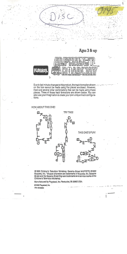

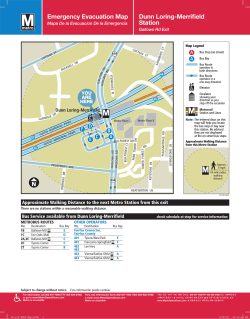

© Copyright 2026