
Stepping into the spotlight - The American Ceramic Society
bulletin AMERICAN CERAMIC SOCIETY emerging ceramics & glass technology MAy 2015 Chalcogenide glass microphotonics: Stepping into the spotlight Glass-ceramics’ 60-year evolution • Peering into the past – Telescope glass • St. Louis/RCD highlights • th Meetings: 11 CMCEE, Cements Division • HSC CHEMISTRY MAKES ELEMENTS WORK FOR YOU Outotec HSC Chemistry 8 Outotec’s chemical reaction and equilibrium software HSC Chemistry is the world’s favorite thermochemical and mineralogical toolbox with a versatile flowsheet simulation module. All calculations and simulations are in an easyto-use format. The current version HSC 8 contains altogether 24 calculations modules and a database with over 28 000 chemical species. [email protected] www.outotec.com/HSC Sustainable use of Earth’s natural resources contents May 2015 • Vol. 94 No. 4 feature articles Chalcogenide glass microphotonics: Stepping into the spotlight . . . . . . . . . . 24 Juejun Hu, Lan Li, Hongtao Lin, Yi Zou, Qingyang Du, Charmayne Smith, Spencer Novak, Kathleen Richardson, and J. David Musgraves Integrated photonics on flexible substrates and on-chip infrared spectroscopic sensing expand new applications for chalcogenide glasses beyond phase change data storage and moldable infrared optics. An analysis of glass–ceramic research and commercialization . . . . . . . . . . . 30 Maziar Montazerian, Shiv Prakash Singh, and Edgar Dutra Zanotto Distinct properties of glass–ceramics give them unique applications in domestic, space, defense, health, electronics, architecture, chemical, energy, and waste management. cover story Peering into the past: What early telescopes reveal about glass technology and scientific evolution . . . . . . . . . . . . . . . . . . . . . . . . . . . . . . . . . . . . 36 April Gocha Corning Museum of Glass curator Marvin Bolt discusses how studying early telescopes provides a glimpse into the evolution of science, birth of glass science, and world history. Chalcogenide glass microphotonics: Stepping into the spotlight Credit: Juejun Hu – page 24 Nonlinear elasticity of silica fibers studied by in-situ Brillouin light scattering in two-point bend test . . . . . . . . . . . . . . . . . . . . . . . . . . . . . . . . . . . . . . 40 Michael Guerette and Liping Huang In-situ Brillouin light-scattering shows that an expression including the fifth-order term is required to capture both minimum in compression and maximum in tension in the elastic modulus of silica glass. meetings GOMD-DGG 2015: Glass & Optical Materials Division and Deutsche Glastechnische Gesellschaft Joint Meeting . . . . . . . . . . . . . . . . . . . . . . . . . . . . . . 44 11th CMCEE: International Conference on Ceramic Materials and Components for Energy and Environmental Applications . . . . . . . . . . . . . . . . . 46 6th Advances in Cement-based Materials . . . . . . . . . . . . . . . . . . . . . . . . . . . . . . . 48 Meeting highlights: ACerS St. Louis Section/Refractory Ceramics Division’s 51st Annual Symposium . . . . . . . . . . . . . . . . . . . . . . . . . . . . . . . . . 49 columns Deciphering the Discipline . . . . . . . . . . . . . . . . . . . . . . . . . . . . . . . . . . . . . . . . . . . 56 feature An analysis of glass–ceramic research and commercialization Credit: Schott North America – page 30 departments Peter Robinson Industry or research? Engineering alternative commercial careers News & Trends . . . . . . . . . . . . . 3 resources Ceramics in Energy . . . . . . . . . 15 New Products . . . . . . . . . . . . . . . . . . . . . . . . . . . . . . . . . . . . . . . . . . . . . . . . . . . . . Calendar . . . . . . . . . . . . . . . . . . . . . . . . . . . . . . . . . . . . . . . . . . . . . . . . . . . . . . . . . . Classified Advertising . . . . . . . . . . . . . . . . . . . . . . . . . . . . . . . . . . . . . . . . . . . . . . . Display Advertising Index . . . . . . . . . . . . . . . . . . . . . . . . . . . . . . . . . . . . . . . . . . . American Ceramic Society Bulletin, Vol. 94, No. 4 | www.ceramics.org ACerS Spotlight . . . . . . . . . . . . 10 50 52 53 55 Ceramics in the Environment . . . . . . 16 Advances in Nanomaterials. . . 17 Research Briefs. . . . . . . . . . . . 18 1 AMERICAN CERAMIC SOCIETY bulletin Editorial and Production Eileen De Guire, Editor ph: 614-794-5828 fx: 614-794-5815 [email protected] April Gocha, Associate Editor Jessica McMathis, Associate Editor Russell Jordan, Contributing Editor Tess Speakman, Graphic Designer Editorial Advisory Board contents May 2015 • Vol. 94 No. 4 Connect with ACerS online! http://bit.ly/acerstwitter http://bit.ly/acerslink http://bit.ly/acersgplus http://bit.ly/acersfb http://bit.ly/acersrss Finn Giuliani, Chair, Imperial College London G. Scott Glaesemann, Corning Incorporated John McCloy, Washington State University C. Scott Nordahl, Raytheon Company Fei Peng, Clemson University Rafael Salomão, University of São Paulo Eileen De Guire, Staff Liaison, The American Ceramic Society Customer Service/Circulation In your hand and on the go! ph: 866-721-3322 fx: 240-396-5637 [email protected] Advertising Sales There are now three great ways to read all of the good stuff inside this month’s issue of the Bulletin! National Sales Mona Thiel, National Sales Director [email protected] ph: 614-794-5834 fx: 614-794-5822 On-the-go option #1: Download the app from the Google Play store (Android tablet and smartphones) or the App Store (iOS tablets only). Europe Richard Rozelaar [email protected] ph: 44-(0)-20-7834-7676 fx: 44-(0)-20-7973-0076 Equally mobile option #2: Download a PDF copy of this month’s issue at ceramics.org and save it to your smartphone, tablet, laptop, or desktop. Executive Staff Charles Spahr, Executive Director and Publisher [email protected] Teresa Black, Director of Finance and Operations [email protected] Eileen De Guire, Director of Communications & Marketing [email protected] Marcus Fish, Development Director Ceramic and Glass Industry Foundation [email protected] Sue LaBute, Human Resources Manager & Exec. Assistant [email protected] Mark Mecklenborg, Director of Membership, Meetings & Technical Publications [email protected] Officers Kathleen Richardson, President Mrityunjay Singh, President-Elect David Green, Past President Daniel Lease, Treasurer Charles Spahr, Secretary Board of Directors Michael Alexander, Director 2014–2017 Keith Bowman, Director 2012–2015 Geoff Brennecka, Director 2014–2017 Elizabeth Dickey, Director 2012–2015 John Halloran, Director 2013–2016 Vijay Jain, Director 2011–2015 Edgar Lara-Curzio, Director 2013–2016 Hua-Tay (H.T.) Lin, Director 2014–2017 Tatsuki Ohji, Director 2013–2016 David Johnson Jr., Parliamentarian Optimized for laptop/desktop option #3: From your laptop or desktop, flip through the pages of this month’s electronic edition at ceramics.org. Credit: Smoking Apples; Flickr; CC BY-SA 2.0 Want more ceramics and glass news throughout the month? Subscribe to our e-newsletter, Ceramic Tech Today, and receive the latest ceramics, glass, and Society news in your inbox each Tuesday, Wednesday, and Friday. Sign up at http://bit.ly/acersctt. Top Tweets Have you connected with @acersnews on Twitter? Here are some recent top posts: Star power Check out ACerS member Valerie Wiesner in this Women’s History Month profile from @NASA! http://bit.ly/1FezckH Supersonic security Glass fibers weave ballistic panels to protect supersonic vehicle from @MorganAdvanced http://bit.ly/1O5RBnR At least you’re getting paid? The top 10 worst jobs In science (via @PopSci) http://bit.ly/1E5icLa American Ceramic Society Bulletin covers news and activities of the Society and its members, includes items of interest to the ceramics community, and provides the most current information concerning all aspects of ceramic technology, including R&D, manufacturing, engineering, and marketing. American Ceramic Society Bulletin (ISSN No. 0002-7812). ©2015. Printed in the United States of America. ACerS Bulletin is published monthly, except for February, July, and November, as a “dual-media” magazine in print and electronic formats (www.ceramicbulletin.org). Editorial and Subscription Offices: 600 North Cleveland Avenue, Suite 210, Westerville, OH 43082-6920. Subscription included with The American Ceramic Society membership. Nonmember print subscription rates, including online access: United States and Canada, 1 year $135; international, 1 year $150.* Rates include shipping charges. International Remail Service is standard outside of the United States and Canada. *International nonmembers also may elect to receive an electronic-only, email delivery subscription for $100. Single issues, January–October/November: member $6 per issue; nonmember $15 per issue. December issue (ceramicSOURCE): member $20, nonmember $40. Postage/handling for single issues: United States and Canada, $3 per item; United States and Canada Expedited (UPS 2nd day air), $8 per item; International Standard, $6 per item. POSTMASTER: Please send address changes to American Ceramic Society Bulletin, 600 North Cleveland Avenue, Suite 210, Westerville, OH 43082-6920. Periodical postage paid at Westerville, Ohio, and additional mailing offices. Allow six weeks for address changes. ACSBA7, Vol. 94, No. 4, pp 1–56. All feature articles are covered in Current Contents. 2 www.ceramics.org | American Ceramic Society Bulletin, Vol. 94, No. 4 news & trends Apple’s gold made stronger with ceramics following in any combination: boron carbide, diamond, cubic boron nitride, titanium nitride (TiN), iron aluminum silicate (garnet), silicon carbide, alumi- Apple’s newest product offering— the Apple Watch—is certain to be no less popular than the rest of its fleet. Fortune estimates that the company could sell anywhere from 8 million to 41 million units. The most basic watch starts at $349. The Apple Watch Edition, a.k.a., the gold one, sells for somewhere between $10,000 and $17,000. “The Edition collection features eight uniquely elegant expressions of Apple Watch,” states the Apple website. “Each has a watch case crafted from 18-karat gold that our metallurgists have developed to be up to twice as hard as standard gold. The display is protected by polished sapphire crystal. And an exquisitely designed band provides a striking complement.” But according to the company’s patent filings, the watch “uses as little gold as possible.” Apple’s application reveals that the extrastrong gold timepiece is an alloy—a metal-matrix composite (MMC) combined with a ceramic powder. The mixture, which according to the filing is 75% gold and 25% ceramic reinforcement, is compressed into a die to achieve near net shape and is heated to sinter the metal and ceramic together. “… the metal-matrix composite can include in addition to gold any of the From slurry to sintering, count on Harrop. Credit: Apple The gold behind the Apple Watch Edition is not pure—it earns strength and durability from ceramic materials. num nitride, aluminum oxide, sapphire powder, yttrium oxide, zirconia, and tungsten carbide. The choice of materials used with the gold in the metal- Tape Casters Binder Burnout Ovens Sintering Kilns The Harrop line of lab and production models feature automatic slurry control with micrometer adjustment to within 0.0001” of wet tape thickness. PLC temperature controlled multi-zone infrared and forced air heating, self-aligning belt drive, and enclosed cabinet for cleanliness. Caster lengths from 6 ft. to more than 100 ft. Harrop forced air conveyor ovens for binder removal from tape cast, pressed or extruded ceramic parts prior to sintering. Stainless steel belt and internals minimize contamination. Work is carried through multiple controlled heating zones. Processing temperatures to 450°C. Weight loss of organics controlled to ± 0.3%. Harrop pusher plate kilns custom designed for precise firing cycles tailored to specified production volumes. Accurate multi-zone heating and atmosphere control. Unique high-density, high-purity refractory design for thermal efficiency and extended service life. Fully automated product handling system. Harrop has been helping hightech ceramic manufacturers for more than 50 years. Learn why we’re the most trusted name in the industry. Call 614-231-3621 to discuss your needs. American Ceramic Society Bulletin, Vol. 94, No. 4 | www.ceramics.org Fire our imagination www.harropusa.com See us at Ceramics Expo, Booth 117 3 news & trends Materials research and research centers get leg up from NSF funding The National Science Foundation recently announced that it will present a dozen Materials Research Science and Engineering Centers (MRSECs) with awards of $1.6 million to $3.3 million Credit: National Science Foundation matrix composite can be based upon many factors, such as color, desired density (perceived as heft), an amount of gold required to meet design/marketing criteria, and so on.” What many might see as purely a cost-cutting measure is really a matter of material performance—the addition of ceramic particles to the MMC makes Apple’s gold “twice as hard” (400 Vickers hardness), more scratch resistant, and less dense. Given the beating a watch can take, a cheaper, stronger, lighter, and more scratchproof model is an advantage for Apple. n NSF will award $56 million to 12 Materials Research Science and Engineering Centers to support cutting-edge research. for multidisciplinary and interdisciplinary materials research and education. The 12 MRSECs will receive a total of $56 million in NSF funding. “These awards are representative of the exquisitely balanced and highly multidisciplinary research portfolio Business news New wing at Corning Museum of Glass opens (cmog.org)…AGC plant in Athus, Belgium, to close (agc.com)…FEI joins University of Ulm and CEOS on SALVE project research collaboration (fei.com) …Alcoa completes acquisition of Tital (alcoa.com)…$2M in support launches Siemens Energy Large Manufacturing Solutions Laboratory (siemens.com)… APC International opens U.S. piezoelectric powder-manufacturing facility (americanpiezo.com)…China’s Fuyao Glass plans to raise up to $950M in IPO (fuyaogroup.com)…Carbo mothballing its ceramic proppant facility in Georgia (carboceramics.com)… Bayer MaterialScience buys composite materials specialist (materialscience. bayer.com)…3M files patent infringement lawsuit to protect dental ceramic coloring technology (3M.com)…Japan Display confirms new plant, source says 4 for Apple (j-display.com)…Alcoa to acquire RTI International Metals (alcoa. com)…Kyocera named 2014 Top Global Innovator by Thomson Reuters (kyocera. com)…Schott suffers fire at Duryea plant (schott.com)…Ferro acquires laser-marking industry leader TherMark (ferro.com)…FCO Power develops SOFC for residential fuel cells in apartments (ecobyfco.com)…Corning Gorilla Glass helps take Gionee slim smartphones to next level (corning.com)…H.C. Starck’s tantalum supply chain compliant with Conflict Free Smelter Program (hcstarck. com)…Air Products and Suzuki Shokan to develop hydrogen fueling for Japan’s material-handling market (airproducts. com)…Goodfellow introduces comprehensive custom manufacturing services (goodfellowusa.com)…Kerneos and Elmin acquire European Bauxites (kerneos.com) n spanning all of the division-supported research areas,” says NSF Division of Materials Research director Mary Galvin in an NSF press release. “These multidisciplinary awards, in particular, will promote areas such as next-generation quantum computing, electronics and photonics, and bio- and soft-materials.” The MRSEC at Columbia University is the newest of the NSFfunded research centers and, according to the release, will have two interdisciplinary research groups (IRGs). “One of the research groups will study how 2-D materials interact to create new physical phenomena to potentially be integrated into electronic devices, and the other research group may establish a new type of periodic table by using molecular clusters to assemble materials, which could generate new electronic and magnetic materials of technological importance.” The other 11 centers “represent melting pots of cutting-edge materials science and engineering.” Many already have well-established IRGs and will add second, third, and fourth groups devoted to the study of materials in a host of applications, including artificial muscles and self-healing materials, superconductors and energy storage, solid-state electronics and low-power switches, optoelectronics and spintronic devices, and materials with bioinspired function. www.ceramics.org | American Ceramic Society Bulletin, Vol. 94, No. 4 Group suggests seven strategies to advance women in science One of the biggest conversations about careers in science, technology, engineering, and mathematics is STEM’s lack of diversity. And because attracting, inspiring, and training the next generation of STEM professionals is vital to future advancements in ceramics and glass, it is an issue that ACerS is dedicated to addressing through expanded outreach initiatives, including the Ceramic and Glass Industry Foundation. Much of that conversation focuses on ways to advance women in science. Even though women have come a long way, research shows that there is still plenty of room for improvement. A working group of 30-plus academic and business leaders organized by the New York Stem Cell Foundation has put forth seven strategies to address financial support, psychological and cultural issues, and collaborative and international initiatives they believe will advance women in an often imbalanced STEM landscape. “We wanted to think about broad ways to elevate the entire field, because when we looked at diversity programs across our organizations we thought that the results were okay, but they really could be better,” says Susan L. Solomon, cofounder and CEO of the New York Stem Cell Foundation and member of the Initiative on Women in Science and Engineering Working Group, in a news release. “We’ve identified some very straightforward things to do that are inexpensive and could be implemented pretty much immediately.” 1. Implement flexible family care spending Make grants gender neutral by permitting grantees to use a certain percentage of grant award funds to pay for childcare, eldercare, or family-related expenses. This provides more freedom for grantees to focus on professional development and participate in the scientific community. 2. Provide “extra hands” awards Dedicate funds for newly independent young investigators who also are primary caregivers to hire technicians, administrative assistants, or postdoctoral fellows. 3. Recruit gender-balanced review and speaker selection committees Adopt policies that ensure that peer review committees are conscious of gender and include a sufficient number of women. 4. Incorporate implicit bias statements For any initiative that undergoes external peer review, include a statement that American Ceramic Society Bulletin, Vol. 94, No. 4 | www.ceramics.org Credit: Maia Weinstock; Flickr CC BY-NC-SA 2.0 They also will have a more defined focus on education, particularly at the Columbia MRSEC, where the university and its partners will work to develop outreach activities for K–12 schools in the area. For more information, go to www. mrsec.org. n LEGO’s female scientist set advanced sales last summer, but what can be done in terms of real-world advancement for women in STEM? Sealing Glass Solutions from Mo-Sci Sealing Glass Excellent wetting and bonding to both metal and ceramics Glass is homogeneous, with no crystals and no significant elements from metal or ceramics diffusing into glass The innovative staff at Mo-Sci will work with you to design and develop your project See us at Ceramics Expo, Booth 116 ISO 9001:2008 • AS9100C www.mo-sci.com • 573.364.2338 5 describes the concept of implicit bias to reviewers and reiterates the organization’s commitment to equality and diversity. 5. Focus on education as a tool Academic institutions and grant makers must educate their constituents and grantees on the issues women face in science and medicine. For example, gender awareness training should be a standard component of orientation programs. 6. Create an institutional report card for gender equality Define quantifiable criteria to evaluate gender equality in institutions on an annual basis. For instance, report cards may ask for updates about the male to female ratio of an academic department or the organization’s policy regarding female representation on academic or corporate committees. 7. Partner to expand upon existing searchable databases of women in science, medicine, and engineering Create or contribute to databases that identify women scientists for positions and activities that are critical components for career advancement. “The issues in science, technology, engineering, and medicine are the kinds of challenges that we as a society face, and we need to have 100 percent of the population—both genders—have an opportunity to participate,” Solomon says. The paper, published in Cell Stem Cell, is “Seven actionable strategies for advancing women in science, engineering, and medicine,” (DOI: 10.1016/j. stem.2015.02.012). n Glass fibers weave supersonic strength into ballistic panels for world’s fastest vehicle The current land speed record rests at 763 mph, but if the Bloodhound Project has its way, the record will not be resting for much longer. The team of United Kingdom-based engineers is working on a new supersonic rocket-powered car they hope will obliterate the world record by rocketing to 1,000 mph. 6 Credit: BLOODHOUND SSC—1,000 mph car; YouTube news & trends An engineer at Morgan Advanced Materials holds a projectile used to test its glass-fiber composite ballistic panels. According to the website, Bloodhound can accelerate from 0 to 1,000 mph in a mere 55 seconds thanks to its whopping 135,000 hp—the equivalent hp of more than 84 of the most powerful Lamborghinis. At those speeds, the car will experience 20 tons of drag, and, if it were fired directly into the air, the car would reach an altitude of 25,000 feet. The Bloodhound team says that the car uses solid aluminum wheels because standard rubber tires would peel off at speeds of about 400 mph. Engineers forged Bloodhound’s solid aluminum wheels so that the aluminum grains “radiate out like the spokes of a wheel.” But rotating at up to 10,200 rpm, or 170 rps, and experiencing 50,000 radial g of force at the rim, the wheels still could fail. So, to protect vehicle and driver hurtling thought the Kalahari dessert at those ridiculously fast speeds, Morgan Advanced Materials engineered glass composite ballistic panels that will protect the car’s carbon composite cockpit sides from all assaults. The panels are composed of millions of glass fibers woven together into a strong mat that can absorb the energy of projectiles bombarding the cockpit at speeds of up to 980 m/s. To test the ballistic panels, Morgan’s engineers blast a simulated piece of Bloodhound’s wheel at the panels. That piece is the largest size they say could break off from the solid aluminum wheels. How did the glass hold up? See for yourself at bit.ly/1BQExw8. n NIST awards $26 million to American manufacturing centers Creating and retaining jobs, turning losses to profits, and implementing processes that improve the efficiency and output of American manufacturers is not something that can be done overnight. It also is not something that can be done without the backing of the private and public sectors. The National Institute of Standards and Technology recently reaffirmed its commitment to small- and medium-sized manufacturers through the awarding of cooperative agreements to 10 nonprofit organizations and universities who oversee Hollings Manufacturing Extension Partnership (MEP) centers located throughout the U.S. (Colorado, Connecticut, Indiana, Michigan, New Hampshire, North Carolina, Oregon, Tennessee, Texas, and Virginia). The 10 will receive a 60% bump in funding—$26 million total—to design new services and increase the number of manufacturers served by MEP programs. “We are excited to award new agreements that bring increased funding levels to better meet the needs of manufacturers in these 10 states,” says acting undersecretary of Commerce for Standards and Technology and acting NIST director Willie May in a NIST press release. “These awards will allow the centers to help more manufacturers reach their goals in growth and innovation, which will have a positive impact on both their communities and the U.S. economy.” These funds do have a pretty impressive ROI for U.S. taxpayers. According to NIST, MEP generates $19 in new sales for every federal dollar that is invested—an annual increase of $2.5 billion—and each federal investment of $2,001 creates one manufacturing job. Congratulations to the award recipients: www.ceramics.org | American Ceramic Society Bulletin, Vol. 94, No. 4 An new dimension in Dilatometry NanoEye An new dimension in Dilatometry Credit: Canadian Pacific; Flickr CC BY-NC 2.0 at s live e r u t fea 00 ll the th #1 o o b See a po at ics Ex tures live Ceram ea NIST has awarded $26 million to help give American manufacturers an edge. •Colorado: Manufacturer’s Edge (Boulder)—$1,668,359; •Connecticut: CONNSTEP Inc. (Rocky Hill)—$1,476,247; •Indiana: Purdue University/Indiana MEP (Indianapolis)—$2,758,688; •Michigan: Industrial Technology Institute/Michigan Manufacturing Technology Center (Plymouth)—$4,299,175; •New Hampshire: New Hampshire Manufacturing Extension Partnership (Concord)—$628,176; •North Carolina: North Carolina State University/North Carolina Manufacturing Extension Partnership (Raleigh)—$3,036,183; •Oregon: Oregon Manufacturing Extension Partnership (Tigard)—$1,792,029; •Tennessee: University of Tennessee, Center for Industrial Services/Tennessee Manufacturing Extension Partnership (Nashville)—$1,976,348; •Texas: The University of Texas at Arlington/Texas Manufacturing Assistance Center (Arlington)—$6,700,881; and •Virginia: A.L. Philpott Manufacturing Extension Partnership/GENEDGE Alliance (Martinsville)—$1,722,571. To learn more about the centers or the awards, go to www.nist.gov/mep/ awards-support-manufacturing.cfm. n University of Arizona to offer new Master of Engineering in Innovation, Sustainability, and Entrepreneurship degree The University of Arizona will launch a new Master of Engineering in Innovation, Sustainability, and Entrepreneurship (ME-ISE) degree in fall 2015. According to the university’s website, this “technical MBA” will offer a combination of business-oriented classes and engineering courses to help engineers bridge the gap between innovative ideas and sus- tainable economic development strategies. “The world is changing in terms of the need for new products and technologies that can be designed to be sustainable throughout their entire life cycle, from manufacturing through ultimate disposal,” says Bob Rieger, associate director of the program. “The Master of Engineering in Innovation, American Ceramic Society Bulletin, Vol. 94, No. 4 | www.ceramics.org f #100 ll the ooth b See a o p ics Ex Ceram DIL 402 Expedis – Introducing the revolutionary NanoEye technology DIL 402 Expedis – Introducing the revolutionary NanoEye Unique resolution up totechnology 0.1 nm over complete measuring range resolution upforce to 0.1for nmtruly Unique Controlled contact over complete measuring range linear measurements contact force for truly Controlled Maintenance-free linear measurements Maintenance-free Plus: Automatic detection of sample length Plus: Software-supported sample placement Automatic detection of sample length “Multi-Touching” Double furnace for more flexibility “Multi-Touching” Software-supported sample placement Double furnace for more flexibility DIL 402 Expedis Supreme DIL 402 Expedis Supreme NETZSCHInstruments InstrumentsNorth North America, NETZSCH America, LLCLLC 129Middlesex MiddlesexTurnpike Turnpike 129 Burlington,MA MA01803-3305, 01803-3305, USA Burlington, USA Tel.:(+1) (+1)781 781272 2725353 5353 Tel.: [email protected] [email protected] 7 www.netzsch.com www.netzsch.com news & trends Sustainability and Entrepreneurship degree from the University of Arizona is designed to teach those skills and tools to the material science community.” Rieger, who is understandably eager to talk about the new ME-ISE degree, was kind enough to respond to a request for more detail. Q. Why now? A. We believe the disciplines associated with the field of materials science, like all advanced technologies, are reaching a critical juncture. Identification of innovative technologies that can be commercialized, development into sustainable products, and the myriad legal, competitive, and regulatory issues surrounding this have become increasing complex. In order to be first to market with new products in today’s world, you need to move fast. This means the luxury of exploring every innovation and conducting every test imaginable before deciding whether there is a chance of commercial success is no longer a workable business model. Rather, tion, water use and management, energy generation, and advanced manufacturing. Being situated in the southwest, these issues have been important for a historically long period. The ability to study and manage materials development from their initial extraction through to an advanced, innovative product is the result of our history and investment in faculty and physical laboratory and prototype manufacturing resources. In addition, the College of Engineering has acknowledged expertise through their offering of engineering management and systems integration curricula developed by industry partners, such as Raytheon Corporation. in addition to superior technical skills, you also need the business skills to rapidly sift through many innovations to identify those that have the greatest chance of success. Concurrently, you need to be evaluating the regulatory, intellectual property, sustainable manufacturing, and competitive landscapes. Both technical and business tools exist that allow an individual to predict and optimize these issues without having to perform laborious tests. The new ME-ISE degree at the University of Arizona teaches these skills and tools. This is very important for those people wishing to start their own companies (entrepreneurs) and those responsible in a structured corporate environment for developing new products (intrepreneurs). Q. When do you plan to begin offering the ME-ISE degree? A. We are currently in the process of accepting applications for our inaugural class to begin in fall 2015. The course of study consists of 30 credit hours, roughly split between technical classes and business and management classes. One unique feature of our program is that while it is designed as a residence program, it also has an online counterpart. At present, approximately 70% of the content is available online, with the remaining to be activated within the next 18 months. We feel this online component makes the ME-ISE degree attractive to the working professional. To learn more about the ME-ISE degree, go to www.sses.arizona. edu/me-ise. n Q. Why the University of Arizona? A. The University of Arizona is uniquely situated, both academically and geographically, to offer the ME-ISE degree. Our School of Material Science and Engineering within the greater College of Engineering hosts centers of excellence in resource extrac- Credit: John Carleton; Flickr CC BY-NC-SA 2.0 Voxel8 introduces the world’s first 3-D electronics printer The University of Arizona’s new master of engineering degree will help materials scientists stack up in the business world. 8 Jennifer Lewis and her Harvard research group have been 3-D printing a vast array of materials—including tissue constructs, strain sensors, and cellular composites. Now Lewis’ group is pioneering 3-D printing in a new direction: electronics. The group is the first to develop and market a 3-D printer that can incorporate conductive inks and plastics into 3-D printed electronics through its spinoff company, Voxel8. The company— founded by former Lewis lab graduate www.ceramics.org | American Ceramic Society Bulletin, Vol. 94, No. 4 ! W E N Alumina ♦ Fused Quartz ♦ Zirconia ♦ Sapphire Crucibles ♦ Furnace Tubes ♦ Thermocouple Insulators Rods ♦ Plates & Disks ♦ Quartz Cuvettes Alumina & Sapphire Sample Pans for Thermal Analysis Custom Components ADVAlue TeChnology 3470 S. Dodge Blvd., Tucson, AZ 85713 Tel: 520-514-1100 ♦ Fax: 520-747-4024 [email protected] ♦ www.advaluetech.com 24-hour Shipment of Many In-stock Standard Sizes Custom Fabrication for Special Requests Credit: Voxel8 students Michael Bell and Travis Busbee—uses core technology based off of a decade of research in Lewis’ lab. “Voxel8 exists to disrupt the design and manufacture of electronic devices by providing new functional materials with a novel 3-D printing platform,” according to the company’s website. Voxel8’s printer incorporates interchangeable printheads that pneumatically dispense multiple materials. Its highly conductive silver ink has a bulk electrical resistivity less than 5.0 × 10⁻⁷ Ω∙m, which the company says is more than 5,000 times more conductive than standard carbon-based inks used in 3-D printing and 20,000 times more conductive than the best conductive-filled thermoplastic filaments. In addition to the ink’s conductive superiority, it can be printed at room temperature through a 250-μm nozzle, affording compatibility with a wide range of materials. And the ink does not require a supportive substrate. “Our inks can hold their shape, span large gaps, and connect to electrical devices, such as TQFP chip packages, without short circuiting,” the website states. Payment of $8,999 will fast-track buyers to the front of the line to get the first of the 3-D electronics printers and early access to new materials, according to the website. The website also hints that the team is not done with the printer’s capabilities yet: “Our initial efforts have focused primarily on conductive inks. However, we have many new materials in the pipeline for future release, starting with advanced matrix materials. The modularity of our cartridge system will allow designers and engineers to use the same printer to print many materials with widely varying electrical and mechanical properties … Voxel8 will leverage ink designs from the Lewis research group, including those that enable 3-D printing of resistors, dielectrics, stretchable electronics and sensors, and even lithium–ion batteries.” For more information, visit www.voxel8.co. n A functional electronic quadcopter 3-D-printed with the new Voxel8 electronics printer. American Ceramic Society Bulletin, Vol. 94, No. 4 | www.ceramics.org See us at Ceramics Expo, Booth 210 9 acers spotlight Society and Division news Welcome to our newest Corporate Member! ACerS recognizes organizations that have joined the Society as Corporate Members. For more information on becoming a Corporate Member, contact Megan Bricker at mbricker@ceramics. org, or visit www.ceramics.org/corporate. Niokem Inc. Waynesville, N.C. www.niokem.com What's new in ancient glass research? Alcoa refractories manager and ACerS Past President, Fellow, and Distinguished Life Member George MacZura dies at 85 George MacZura, who made his career developing innovative refractory aluminas and cements at Alcoa, died on March 13 at the age of 85. After graduating from University of Missouri-Rolla (now the Missouri University of Science and Technology) in 1952, MacZura accepted a position with Alcoa’s chemical research plant in East St. MacZura Louis, Ill. He expected to work for a few years, gain some experience, and move on to new opportunities. Instead, “a few years” became 44 years, he recounts in a 1999 ACerS Bulletin article. “As it turned out, there was always a new challenge in research that intrigued me and [the move] never happened.” Over the course of his career, he traveled to more than 50 countries to introduce new products and teach customers how to use them. At the time of his retirement in 1997, he held the position of international refractories market development manager. MacZura led the first Unified International Technical Conference on Refractories (UNITECR) in 1989 and served as the first president of UNITECR. MacZura was a member of the Refractories Ceramics Division. In addition to serving as Society president 1992–1993, he was an ACerS Fellow and was elevated to Distinguished Life Member in 2009. MacZura received the St. Louis Section’s Theodore J. Planje Award, the Pittsburgh Section’s Albert Victor Bleininger Memorial Award, and the National Institute of Ceramic Engineers’ ACerS/NICE Greaves– Walker Award. n Credit: Vlasta2; Flickr; CC BY-NC-ND 2.0 Ceradyne founder and ACerS Distinguished Life Member Joel Moskowitz dies at 75 May 17, 2015 | 8:30 a.m. – 5:20 p.m. Hyatt Regency Miami Explore glass's past and present during this one-day workshop hosted by ACerS Art, Archaeology, and Conservation Science Division, following the American Institute for Conservation meeting. Register at ceramics.org. 10 Joel Moskowitz—the man known for saving the lives of soldiers in combat—lost his battle against cancer on March 15 at the age of 75. Originally from Brooklyn, N.Y., Moskowitz studied ceramic engineering at Alfred University. In 1967, after working for a few years as a research engineer at Interpace Corporation, he and a business partner pulled together $5,000 to start the company that became Ceradyne. Moskowitz The business grew to become an international, publicly traded company employing nearly 3,000 at locations in the United States, Canada, China, and Germany, with annual revenues of $500 million. In fall 2012, 3M (St. Paul, Minn.) acquired Ceradyne in a deal valued at approximately $860 million. With the sale, Moskowitz retired from his position as CEO of the company he led for 45 years. Ceradyne was founded to develop, manufacture, and market advanced structural ceramics for defense, industrial, and consumer applications, and is best known for its boron carbide ceramic armor for soldiers and vehicles. “We’re saving American lives,” Moskowitz often remarked in interviews. Moskowitz was instrumental in launching The Ceramic and Glass Industry Foundation, the Society’s philanthropic arm dedicated to education and workforce development. As founding chair of CGIF, he helped define its mission and vision. He was an enthusiastic ambassador, advocate, and supporter for the CGIF. Moskowitz joined ACerS in 1958 and was elevated to Distinguished Life Member in 2012. n www.ceramics.org | American Ceramic Society Bulletin, Vol. 94, No. 4 MCARE 2015 attracts global leaders in alternative energy (From left) Do-Heyoung Kim, MCARE 16 Secretary General; Zhong Lin Wang, Plenary Speaker; Xavier Obradors, Plenary Speaker; and Yoon-Bong Hahn, MCARE 2015 and 2016 Co-Chair. Materials Challenges in Alternative & Renewable Energy (MCARE) 2015 was held February 24–27 in Jeju, South Korea. This interdisciplinary conference was designed to bring together leading global experts, providing a unique opportunity for communication and collaboration in the field of advanced materials for new and renewable energy. MCARE 2015 consisted of 10 symposia, including a Young Scientists' Forum of Future Energy Materials and Devices. Conference organizers received a total of 380 abstracts— including 140 invited papers, 4 plenary lectures, 14 keynote talks, and 121 invited talks—which contributed to the high quality and level of presentations. The meeting attracted around 400 attendees, half of which hailed from outside Korea, from 26 countries. n and glass products. Although the new Manufacturing Division will encompass the former Whitewares and Materials Division, its focus will be on meeting the much broader needs of today’s manufacturers who produce or use ceramic and glass materials. In addition to enhancing networking opportunities, the Manufacturing Division will address new processes and techniques, sustainability, and business and environmental issues. Further, the Division plans to provide quality technical information through meeting programming, technical content in ACerS publications, and short courses and workshops to educate industry personnel and promote recruitment and hiring of engineers into ceramic and glass manufacturing companies. “Bringing ceramic and glass manufacturing back into the spotlight has been a strategic goal of the Society for a long time," Carty says. "And launching it at the new Ceramics Expo in April was perfect timing since the audience there is primarily from industry. We look forward to pairing the Division and the Expo together for a long time and helping them both grow in size and influence in the ceramics and glass manufacturing community.” ACerS forms new Manufacturing Division to meet industry needs ACerS has formed a new Manufacturing Division to address the needs of members and prospective members worldwide who work in the ceramics and glass manufacturing industry and its supply chain. William Carty, Alfred University, will serve as inaugural chair of the new Division. Carty proposed the new Division so that manufacturing companies and their employees have a more defined Division within the Society. Carty and several supportive members from industry began by developing a plan for transforming the inactive Whitewares and Materials Division into a new Manufacturing Division, a proposal that the Board of Directors has endorsed. The new Division will address information needs of the ceramic and glass manufacturing industry, including manufacturers; suppliers of raw-material; and producers of forming and finishing equipment, kilns, furnaces, quality-control instrumentation, and all other devices used to manufacture ceramic American Ceramic Society Bulletin, Vol. 94, No. 4 | www.ceramics.org See us at Ceramics Expo, Booth 340 303-433-5939 11 acers spotlight Society and Division news (continued) ACerS president Kathleen Richardson echoes Carty's comments and adds, “I see the new Division as a much needed bridge between academia and industry and as a way that the two communities can engage. As both an academic and a business entrepreneur, I see many opportunities for interaction, and I encourage all members to get involved in the Manufacturing Division.” Members of the Whitewares and Materials Division voted on the new name and mission, and the vote was overwhelmingly in favor of the change. Members of the Whitewares and Materials Division will automatically become members of the new Manufacturing Division. The Division also elected a new slate of officers: Chair: William Carty, Alfred University Chair-Elect: Nik Ninos, Calix Ceramic Solutions Vice-Chair: Ed Reeves, Reeves Consulting Secretary: Keith DeCarlo, Blasch Precision Ceramics Inc. Final Board approval took place on March 25, 2015. The Manufacturing Division executive committee will hold an initial planning meeting at Ceramics Expo in Cleveland, Ohio, April 29, 2015, where it will host a small lunch with industry representatives. Get involved: Join for free! Become a member of the Manufacturing Division at no charge for one year and help set the direction during this important inaugural year. Contact Marcia Stout at [email protected] or 614-794-5821 to join. n ACerS and GOMD announce 2015 lecture awards ACerS and the Glass and Optical Materials Division will honor its 2015 lecture award recipients during the joint meeting of ACerS GOMD–DGG, May 17–21, Miami, Fla. For more information, visit ceramics.org/meetings. Darshana and Arun Varshneya Frontiers of Glass Science Lecture Wednesday, May 20, 8 a.m. Sabyasachi Sen, professor of materials science, University of California, Davis, Structural aspects of relaxational dynamics in glasses and supercooled liquids. Previous literature has Sen primarily treated dynamic processes associated with viscous and diffusive transport in glass-forming liquids as macroscopic phenomena. These phenomena are often investigated using bulk relaxation experiments that typically lack a direct understanding of atomicscale processes. NMR spectroscopy has the unique ability to combine timescale and structural information to probe the mechanisms of molecular relaxation dynamics in glasses and viscous liquids. Sen will present an overview of recent work from his laboratory involving the application of NMR spectroscopic techniques to address the nature and timescale of various thermally driven 12 configurational changes in a wide variety of inorganic and organic glasses and supercooled liquids and their relationship to macroscopic relaxation and transport processes. Sen obtained his Ph.D. in geochemistry from Stanford University. He has held positions at the University of Wales Aberystwyth (United Kingdom), and Corning Incorporated (Corning, N.Y.). He joined the Materials Science and Engineering Department at the University of California, Davis in 2004. He has authored and coauthored more than 150 scientific papers and 7 U.S. patents. Sen’s research interests include the application of state-of-the-art spectroscopic and diffraction techniques to understand structure and dynamics in amorphous materials, including glasses and glass-forming liquids, fast ion conduction in crystalline solid oxide electrolytes, battery materials, and ionic liquids. Darshana and Arun Varshneya Frontiers of Glass Technology Lecture Thursday, May 21, 8 a.m. Steven B. Jung, chief technology officer, Mo-Sci Corporation, The present and future of glass in medicine. Glass already is used in medical applications from cancer treatment Jung to tissue regeneration, but the future of medical glass will require advances in chemical composition, shape, form, and processing to continue to improve treatment options. The beauty of glass is that it can obtain almost any characteristic—durable, degradable, solid, porous, and more. The uniqueness of the material properties of glass ultimately makes way for innovative medical devices. Jung’s talk will focus on present advances in hard- and soft-tissue regeneration and why glass materials will remain a viable and growing option for the future of healing. Jung received a Ph.D. in materials science and engineering from the Missouri University of Science and Technology (Rolla, Mo.), where he studied bioactive glass scaffolds for hard- and soft-tissue regeneration. He is an inventor on 11 U.S. patents and about 50 pending U.S. and international patents in biomaterials. Jung is currently chief technology officer at specialty and healthcare glass manufacturer Mo-Sci Corporation (Rolla, Mo.). Stookey Lecture of Discovery Monday, May 18, 8 a.m. N. B. Singh, University of Maryland, Baltimore County, Development of multifunctional chalcogenide and chalcopyrite crystals and glasses. www.ceramics.org | American Ceramic Society Bulletin, Vol. 94, No. 4 During the past few decades, much research has developed glass and single-crystal materials for optical applications for visible and near–infrared wavelengths. However, for midwave and long-wave infrared regions, efficient materials continue to be needed. Singh will Singh summarize his research efforts to identify these materials and characterize their performance for a variety of applications. The talk will focus on growth and performance of bulk and quasi-phase-matched materials for laser development and acousto-optical hyperspectral imaging. Singh is a Fellow of ASM, International Society of Optics and Photonics, Optical Society of America, and Royal Society of Chemistry. Before his position at the University of Maryland, Singh was a senior consulting engineer at Northrop Grumman Electronic Systems (Baltimore, Md.). His research interests include development of bulk, thin-film, and nanoengineered materials, acousto-optic imagers and spectral sensors, dielectric materials, structures for mid-infrared lasers, organic materials for nonlinear optical applications, wide bandgap materials for microelectronics, and radiation detector materials. George W. Morey Award Lecture Tuesday, May 19, 8 a.m. Jianrong Qiu, chair professor, South China University of Technology, Control of the metastable state of glasses. Glass’s metastable state and topological network structure provide the material with good homogeneity, variable composition, and ease of shaping and doping. Qui’s research focuses on Qiu enhancing the properties of glass by manipulating its metastable nature through precise control of microstructure. In his talk, Qui will highlight recent research on the design and control of optical properties of glass through fast cooling, crystallization, and phase separation, including demonstration of ultra-broadband near-infrared emission for optical amplification and tunable lasers. The talk also will introduce results of 3-D printing of nanostructures or microstructures inside glasses by femtosecond lasers. Qiu received his Ph.D. from the noncrystalline solids group at Okayama University (Japan). Qui’s research has focused on understanding the nature of glass and development of techniques for realization of novel glass functions, with current research in functional glasses, femtosecond laser interactions with glass, and inorganic luminescent materials. He has published more than 500 papers in fundamental areas of glass science and technology. Qiu is currently chair professor of Cheung Kong Scholars Programme at South China University of Technology (China). Norbert J. Kreidl Award for Young Scholars Tuesday, May 19, noon Michael J. Guerette, postdoctoral researcher, Rensselaer Polytechnic Institute, Structure and nonlinear elasticity of silica American Ceramic Society Bulletin, Vol. 94, No. 4 | www.ceramics.org glass fiber under high strains. Guerette has developed in-situ high-resolution Raman and Brillouin light-scattering techniques to study structural signatures and elastic moduli of silica glass fiber under tensile and compressive strains. His work has established Guerette a two-point bend test to determine the neutral axis of a bent fiber by traversing the apical cross-section, which allows for more accurate calculations of strain and stress of a bent fiber. Guerette’s results contribute to a fundamental understanding of the structure and elastic properties of glasses under high strain conditions, which is of critical importance for developing strong glasses. Guerette received a B.A. in physics from the University of Southern Maine (Portland, Maine), where he studied optical techniques for materials characterization, and a Ph.D. in materials engineering from Rensselaer Polytechnic Institute (Troy, N.Y.). He is researching structure and property relationships of silica glass that are subjected to extreme temperature, pressure, and strain. Guerette uses extreme conditions as synthesis parameters and subsequent testing environments to allowed him to gain a unique understanding of the evolution of structure and properties of this archetypal glass former. n ENGINEERED SOLUTIONS FOR POWDER COMPACTION Gasbarre | PTX-Pentronix | Simac HIGH SPEED, MECHANICAL, AND HYDRAULIC POWDER COMPACTION PRESSES FOR UNPRECEDENTED ACCURACY, REPEATABILITY, AND PRODUCTIVITY MONOSTATIC AND DENSOMATIC ISOSTATIC PRESSES FEATURING DRY BAG PRESSING See us at Ceramics Expo, Booth 319 814.371.3015 www.gasbarre.com 13 acers spotlight Award deadlines Southwest Section to hold June meeting Mark your calendars for the 2015 meeting of the Southwest Section of The American Ceramic Society, June 3–5, 2015, at the Radisson Hotel Fossil Creek in Fort Worth, Texas. The program, “Training a New Generation of Ceramic Employees,” will include industry plant trips and technical sessions. A companions’ program for families with children also will be offered. Registration information will be available soon at ceramics.org. n In memoriam William C. Spangenberg Albert E. Paladino Henry E. Hagy John G. Matchulat Some detailed obituaries also can be found on the ACerS website, www.ceramics.org/in-memoriam. Students and outreach Start engineering the winning mug, disc, poster, or talk for MS&T15 contests Do you have an exciting research project? A winning design for a super strong ceramic mug or disc? Start your preparations now to compete in the Material Advantage student contests at MS&T15, October 4–8, Columbus, Ohio. The contests will include: •Undergraduate Student Poster Contest •Undergraduate Student Speaking Contest •Graduate Student Poster Contest •Ceramic Mug Drop Contest •Ceramic Disc Golf Contest For more information, contact Tricia Freshour at [email protected]. n 14 Deadlines for upcoming nominations May 15, 2015 Glass and Optical Materials Division’s Alfred R. Cooper Scholars Award This $500 award encourages and recognizes undergraduate students who have demonstrated excellence in research, engineering, or study in glass science or technology. Electronics Division’s Edward C. Henry Award This award is given annually to an author of an outstanding paper reporting original work in the Journal of the American Ceramic Society or the Bulletin during the previous calendar year on a subject related to electronic ceramics. Electronics Division’s Lewis C. Hoffman Scholarship The purpose of this $2,000 tuition award is to encourage academic interest and excellence among undergraduate students in ceramics/materials science and engineering. The 2015 essay topic is "Electroceramics for telecommunications." July 1, 2015 Engineering Ceramics Division’s James I. Mueller Award This award recognizes the accomplishments of individuals with long-term service to the Division or work in engineering ceramics that has resulted in significant industrial, national, or academic impact. The awardee receives a memorial plaque, certificate, and honorarium of $1,000. Contact Mike Halbig at [email protected] with questions. Engineering Ceramics Division’s Bridge Building Award This award recognizes individuals outside of the United States who have made outstanding contributions to engineering ceramics, including expansion of the knowledge base and commercial use thereof, contributions to visibility of the field, or international advocacy. The award consists of a glass piece, certificate, and an honorarium of $1,000. Contact Soshu Kirihara at [email protected] with questions. Engineering Ceramics Division’s Global Young Investigator Award This award recognizes an outstanding scientist based on contributions to scientific content and to visibility of the field, and advocacy of the global young investigator and professional scientific forums. Candidates must be ACerS members, 35 years of age or younger, and conducting research in academia, industry, or at a government-funded laboratory. The award consists of a glass piece, certificate, and $1,000. Contact Andy Gyekenyesi at Andrew L. [email protected] with questions. September 1, 2015 ACerS 2016 Class of Fellows Nominees need to be at least 35 years old and have been members of the Society at least for the past five years continuously. The nominee also must have letters of support from seven sponsors who are ACerS members. Be sure to adhere to nomination and support letter length guidelines—nominations that do not conform will be returned. Scanned and faxed signature forms are permitted in lieu of original mailed signature forms. Previously submitted nominations may be updated, as long as they do not exceed length limitations. Additional information and nomination forms for these awards can be found at ceramics.org/awards, or by contacting Marcia Stout at [email protected]. n ACerS members save more. For members-only discounts, including savings of up to 34% on shipping, join now at ceramics.org. www.ceramics.org | American Ceramic Society Bulletin, Vol. 94, No. 4 ceramics in energy Researchers from the University of Luxembourg and Japanese electronics company TDK report progress in photovoltaic research—they have developed a highly conductive oxide film that will help solar cells harness more of the sun’s energy. Their undoped zinc oxide film boasts increased infrared transparency and creates a higher current that could make for more efficient devices. According to a university news release, the findings, published in Progress in Photovoltaics, represent the first one-step process to prepare these films and the first time the prepared films are stable in air. “The films made at the Researchers from the University of Luxembourg and TDK have developed a highly conductive oxide film that will help solar cells harness more of the sun’s energy. University of Luxembourg have been exposed to air for one and half years and are still as conductive as when they were fresh prepared,” says Susanne Siebentritt, professor and head of the photovoltaics lab at the University of Luxembourg, in the release. “It is a fantastic result, not only for solar cells, but also for a range of other technologies.” In previous attempts to create a more conductive solar film, impurities—such as aluminum and its free electrons—were added to pure zinc oxide. But additional electrons mean more absorption of infrared light, and less light means less solar energy can pass through the film to generate current. The Luxembourg–TDK team modified the process so that the pure, undoped zinc oxide film would have fewer, fastermoving free electrons even without the addition of aluminum. The team used low-voltage radio frequency (rf) biasing during deposition to make the films more conductive. “The films prepared with additional rf biasing possess lower free-carrier concentration and higher free-carrier mobility than Al-doped ZnO (AZO) films of the same resistivity, which results in a substantially higher transparency in the near-infrared region,” states the paper’s abstract. “Furthermore, these films exhibit good ambient stability and lower high-temperature stability than the AZO films of the same thickness.” The result is a pure film with conductivity comparable to those that contain aluminum, but with better transparency and fewer electrons standing in the way of absorption, says lead author Mate�j Hála. The paper is “Highly conductive ZnO films with high nearinfrared transparency” (DOI: 10.1002/pip.2601). n American Ceramic Society Bulletin, Vol. 94, No. 4 | www.ceramics.org 15 Credit: Susanne Siebentritt; University of Luxembourg Highly conductive, undoped oxide film will help solar cells harness more sunlight ceramics in the environment Optimized microstructure removes cold-start emissions Although catalytic converters significantly reduce vehicle emissions, they efficiently work only when warm. The time required to heat up catalytic converter substrates is called the “light-off” period, and it is estimated that this time period (which lasts for ~30 seconds and up to several minutes) accounts for ~70% of total automobile emissions. Reducing these cold-start emissions is a top priority in the face of tighter emission standards. Corning’s innovators have developed a new product, Flora, with an “optimized material microstructure” that is designed to decrease cold-start emissions. Ken Twiggs, Corning’s innovation program manager for substrates, says in a telephone interview that Flora contains the same cordierite material that the company has modified to improve 16 Secondary electron image showing a glass spherule formed in high-voltage flashover experiments to examine the effect of ash contamination on electrical insulators. Laboratory experiments mimicking volcanic lightning also produced glass spherules.The spherules’ composition consisted of primarily silicon, with lesser amounts of aluminum, calcium, and iron, the authors report in the paper. The researchers speculate that these spherules, called lightning-induced volcanic spherules (LIVS), form in the eruptive atmosphere from volcanic ash when it is heated rapidly during lightning discharge. The intense heat of the discharge, which can reach temperatures of up to 30,000 K, melts and fuses the particles, which quickly cool and form glass. The open-access paper, published in Geology, is “Lightning-induced volcanic spherules” (DOi: 10.1130/G36255.1). n thermal performance by increasing the material’s porosity. Although that usually means consequently decreasing strength, the experts at Corning were able to maintain strength and performance even with increased substrate porosity. The material heats up considerably faster than existent substrates, reducing the light-off period. According to Corning, the new Flora material reduces the mass of the substrate so that it warms up 20% faster than existing ceramic substrates. “The novel material reaches operating temperature quicker than standard substrates, so catalytic converters can clean exhaust emissions earlier without increased fuel or additional precious metal,” according to a Corning press release. n Corning’s new Flora substrates have increased porosity to reduce cold-start automobile emissions. Credit: Corning In addition to the ways humans have figured out how to make glass, glass forms naturally—for example, from volcanic activity, meteorite impacts, and lightning strikes. All of these events can produce not just glass, but small glass spheres, or spherules. New research suggests that natural glass spheres also are born during another natural phenomenon—volcanic lightning. An international team of scientists studied volcanic ash deposits from two recent eruptions: Mount Redoubt, Alaska, in 2009, and Eyjafjallajökull, Iceland, in 2010. Both well-documented eruptions were accompanied by volcanic lightning. The scientists found small glass spherules—on average, about 50 μm in diameter—in ash deposits collected from both volcanos. Although the spherules were few in abundance, composing less than 5% of examined deposits from Mound Redoubt and even less from Iceland (there scientists identified only two spherules), the findings suggest that glass balls can form from volcanic lighting. Credit: Kimberly Genareau Volcanic lightning zaps ash into glass www.ceramics.org | American Ceramic Society Bulletin, Vol. 94, No. 4 advances in nanomaterials Nanomaterials’ grain boundaries absorb defects, lengthen life of nuclear fuel Although previous research has suggested that nanocrystalline ceramics would be more radiation tolerant than bulk (microcrystalline) samples of the same material, the team’s newly published research confirms these suspicions and, importantly, provides the mechanism by which it happens—through reduced accumulation of point defects. Point defects normally form in a material upon irradiation. But accumulation of defects within nuclear fuel negatively affects its behavior and performance and, thus, directly impacts its potential life cycle. Decreasing the accumulation of defects, therefore, would increase nuclear fuel lifetime. Castro and the team studied precisely how defects evolve in response to irradiation, measuring the location and migration of individual defects in microcrystalline and nanocrystalline samples of 10-mol%-yttria-stabilized zirconia. According to Castro, the team used zirconia because it has a similar structure to nuclear fuel uranium dioxide. “We saw very little damage in the nanocrystalline samples, and significant damage in the microcrystalline sample. This is because the grain boundaries in Credit: R. Castro; UC Davis The cost to reload nuclear fuel in a typical 1,000 MWe nuclear reactor that refuels on an 18-month cycle is a staggering $40 million, according to the Nuclear Energy Institute. Therefore, making fuel last longer can save a lot of money, increase plant efficiency and output, and improve safety of nuclear energy. New research from Ricardo Castro, ACerS member and materials science professor at University of California, Davis, and a team of his colleagues is providing important insight into how nanomaterials behave under irradiation, findings that may help significantly extend the life of nuclear fuels. The research team, which recently published its findings in Scientific Reports, also includes ACerS members John Drazin from UC Davis and Terry Holesinger and Blas Uberuaga from Los Alamos National Laboratory. The team examined how nanocrystalline nuclear fuels compare to their microcrystalline counterparts. Although composed of the same material, nanocrystalline and microcrystalline samples have significantly different grain sizes, a feature that the team found greatly impacts the material’s properties after irradiation. Electron micrographs of microcrystalline and nanocrystalline samples of yttria-stabilized zirconia, which develop defects in response to irradiation. V indicates vacancy defect, I indicates interstitial defect. Scale bar shows individual grain size. American Ceramic Society Bulletin, Vol. 94, No. 4 | www.ceramics.org the sample act as sinks for interstitial defects,” Castro says in an email. “That is, nanomaterials accumulate less defects during radiation—a key element to enhance lifetime of nuclear fuel.” “Since more defects means to shorter lifetime, one can expect longer life for nanocrystalline uranium dioxide fuels as compared with regular micrograined fuels,” Castro says. The type of defects was different, too: Although microcrystalline samples had interstitial and vacancy defects, the nanocrystalline samples accumulated only vacancies, which clustered to minimize energy. “In nanocrystalline samples, the probability of the defect ‘finding’ a boundary is much higher, because grains are smaller,” Castro explains. “Boundaries are stable sinks for the interstitials, but produced vacancies are shared between boundary and bulk, since they can form metastable clusters in the bulk. Therefore, in nanocrystalline samples, one cannot find interstitial defects in the crystal—only vacancies. In the microcrystalline samples, we find both, and in much higher concentrations (since only a few defects can actually find a boundary).” Castro explains that the amount of radiation they exposed the test materials to was equivalent to 4.5 years of service life in reactors, despite the fact that nuclear fuels are typically replaced within one year in actual service because of damage considerations and safety precautions. “Since zirconia also finds structural applications, the results can also be used to predict nanoeffects in [nuclear fuel storage conditions, too,] such as core barrels and dry casts. As a reactor vessel, the tested radiation would be equivalent to 21 million years. So again, nanomaterials would be able to resist much longer than microcrystalline samples.” The open-access paper is “Radiation tolerance of nanocrystalline ceramics: Insights from yttria-stabilized zirconia” (DOI: 10.1038/srep07746). n 17 research briefs Limpets—a kind of mollusk—are the latest creatures to inspire advances in materials science research. Massachusetts Institute of Technology researchers recently discovered that some limpet shells contain unique biological photonic structures that are the first known to be made from inorganic, mineralized structures. The research zoomed in on one particular variety of fingernail-sized snail, the blue-rayed limpet. Blue-rayed limpets feature a drab shell adorned with brilliant blue stripes, which make the tiny snails stand out even in murky water of the kelp beds they call home along the coasts of Norway, Iceland, the United Kingdom, Portugal, and the Canary Islands. Although other creatures—such as beetles, butterflies, and birds—also display bright hues, those colors come from photonic structures within the creatures’ shells, scales, or feathers that are composed primarily of organic materials. To investigate the interesting color of blue-rayed limpets’ stripes, researchers first examined the shells Research News Silver–glass sandwich structure acts as inexpensive color filter Northwestern University researchers have created a new technique that can transform silver into any color of the rainbow. Their simple method is a fast, low-cost alternative to color filters currently used in electronic displays and monitors. The filter’s secret lies within its “sandwichlike” structure. The team created a three-layer design, where glass is wedged between two thin layers of silver film. The silver layers are thin enough to allow optical light to pass through, which then transmits a certain color through the glass and reflects the rest of the visible spectrum. By changing the thickness of the glass, the scientists filtered and produced various colors. By making the bottom silver layer even thicker, the scientists found that the structure also acts as a color absorber, because it traps light between the two metal layers. The team demonstrated a narrow bandwidth 18 from the outside. Scanning electron micrographs of the shells’ surface showed no structural differences in the striped regions. Using focused ion beam milling, the researchers then cut out a cross-section of the shell and examined the underlying nanoarchitecture A blue-rayed limpet’s shell still shines underwater. using 2-D and 3-D structural analyses. green light, acting as an optical interferThe findings show that about 30 μm ence filter. And the colloidal spheres below the shells’ striped surface, the served to “absorb transmitted light that shell-standard uniform composition would otherwise desaturate the reflected of stacked calcium carbonate platelets blue color,” according to an MIT press changed. There, the researchers found release. The zigzags reflect only blue wider zigzagged layers of calcium carbon- light, while the remaining light spectrum ate that were underlaid with randomly travels through the shell, where it is arranged spherical colloidal particles. absorbed by the colloidal particles, makFurther analysis of the zigzags’ spacing the blue look bluer. ing and angles revealed that they were “Therefore the absorbing particles optimally arranged to reflect blue and underneath the limpet’s multilayer archi- superabsorber with 97% maximum absorption, which could have potential applications for optoelectric devices with controlled bandwidth, such as narrow-band photodetectors and lightemitting devices. For more information, see www.mccormick.northwestern.edu. pace. Vortexes can form when a magnetic field is applied, but the material’s ultrathin design permits only one row of vortexes to fit within a nanowire, which traps the vortexes in place and prevents current disruption. For more information, see www.jhu.edu. Ultrathin nanowires can trap electron ‘twisters’ that disrupt superconductors Silicon microfunnels increase the efficiency of solar cells Superconductor materials are prized for their ability to carry an electric current without resistance, but this valuable trait can be crippled or lost when electrons swirl into tiny tornadolike formations called vortexes. These disruptive minitwisters often form in the presence of magnetic fields, such as those produced by electric motors. To keep supercurrents flowing at top speed, Johns Hopkins University scientists have figured out how to constrain troublesome vortexes by trapping them within extremely short, ultrathin nanowires. These thin nanowires form one-way highways that allow pairs of electrons to zip ahead at a supercurrent The closely packed arrangement of cones in the eyeball has inspired a team of researchers at Helmholtz-Zentrum Berlin to replicate something similar in silicon as a surface for solar cells and investigate its suitability for collecting and conducting light. Using conventional semiconductor processes, the researchers etched micrometer-sized vertical funnels shoulder-to-shoulder in a silicon substrate. Using mathematical models and experiments, they tested how these types of funnel arrays collect incident light and conduct it to the active layer of a silicon solar cell. The researchers found that funnel-shaped silicon www.ceramics.org | American Ceramic Society Bulletin, Vol. 94, No. 4 Credit: MIT Striped mollusks hide unique photonic structures that may inspire future displays tecture are not the direct origin of the blue color, which is caused by the multilayer architecture,” the authors write in the paper. “The particles rather provide an absorbing background for the multilayer filter to enhance the spectral purity of the reflected blue light.” According to the paper, the chemical composition of the colloidal particles remains unknown. In addition to representing the first known biological photonic structures that are composed of inorganic structures, the authors make another interesting point: The limpet shells are able to incorporate photonic structures without compromising structural integrity. “It’s all about multifunctional materials in nature: Every organism—no matter if it has a shell, or skin, or feathers—interacts in various ways with the environment, and the materials with which it interfaces to the outside world frequently have to fulfill multiple functions simultaneously,” Mathias Kolle, coauthor and MIT mechanical engineering professor, says in the press release. “[Engineers] are more and more focusing on not only optimizing just one single property in a material or device, like a brighter screen or higher pixel density, but rather on satisfying several … design and performance criteria simultaneously. We can gain inspiration and insight from nature.” The researchers speculate that their findings could be used to develop similar smart architectures in customdesigned materials. “Let’s imagine a window surface in a car where you obviously want to see the outside world as you’re driving, but where you also can overlay the real world with an augmented reality that could involve projecting a map and other useful information on the world that exists on the other side of the windshield,” Kolle says in the release. “We believe that the limpet’s approach to displaying color patterns in a translucent shell could serve as a starting point for developing such displays.” The open-access paper, published in Nature Communications, is “A highly conspicuous mineralized composite photonic architecture in the translucent shell of the blue-rayed limpet” (DOI: 10.1038/ncomms7322). n Long-term measurements of ultrastable glass flow cut short with new process structures increase light absorption better than a carpet of nanowires. Further, the arrangement of funnels increases photo-absorption by about 65% in a thin-film solar cell fitted with such an array and is reflected in considerably increased solar cell efficiency, among other improved parameters. For more information, see http:// www.helmholtz-berlin.de. reactions. In tests involving half of the catalytic reaction that takes place in fuel cells, the team discovered versions with about 10% boron and nitrogen were efficient in catalyzing an oxygen reduction reaction, a step in producing energy from feedstocks , such as methanol. For more information, see www.news.rice.edu. rare earths are recovered from the magnesium through vacuum distillation. In the second step, another material is used to bind with and extract the heavier atomic weight rare earths, such as dysprosium. For more information, see www. ameslab.gov. Aerogel catalyst shows promise for fuel cells Graphene nanoribbons formed into a threedimensional aerogel and enhanced with boron and nitrogen are excellent catalysts for fuel cells, even in comparison with platinum, according to Rice University researchers. The team chemically unzipped carbon nanotubes into ribbons and then collapsed them into porous, three-dimensional aerogels, simultaneously decorating the ribbons’ edges with boron and nitrogen molecules. The new material provides an abundance of active sites along the exposed edges for oxygen reduction New process recycles valuable rareearth metals from old electronics Scientists at the Critical Materials Institute (Ames, Iowa) have developed a two-step recovery process that makes recycling rareearth metals easier and more cost effective. Building on previous research work done at the Ames Laboratory, the team has developed a two-stage liquid-metal extraction process that uses differences between the solubility properties of elements to separate out rareearth metals. In the liquid extraction method, scrap metals are melted with magnesium. Lighter atomic weight rare earths, such as neodymium, bind with magnesium and leave the iron scrap and other materials behind. Then American Ceramic Society Bulletin, Vol. 94, No. 4 | www.ceramics.org Researchers from Universitat Autònoma de Barcelona (Spain), University of Rome La Sapienza (Italy), and Politecnico Milano (Italy) have devised a technique to rapidly manufacture “old” glass to mimic glasses aged naturally for millennia and measure viscosity to get a glimpse into very-long-term glass relaxation behavior. Glass is a rigid material with an amorphous structure. The question is whether it behaves like a really viscous liquid, or whether it ceases completely to flow at low temperatures. Current glass theories predict that a glass’s liquidlike molecules stop flowing at a certain low temperature, but from a practical perspective, very high viscosities are nearly impossible to measure. “We managed to measure relaxation times as large as thousands of years, previously inaccessible to experimental determinations, demonstrating the lack of structural arrest at temperature well below the glass transition point or, equivalently, the lack of the viscos- Patented zeolite tech could significantly cut carbon dioxide emissions A new provisionally patented technology from a New Mexico State University researcher could revolutionize carbon dioxide capture and have a significant impact on reducing pollution worldwide. Through research on these zeolitic imidazolate frameworks, or ZIFs, the researcher has synthesized a new subclass of ZIF that incorporates a ring carbonyl group in its organic structure, giving it a vastly greater affinity and selectivity for separating and adsorbing carbon dioxide and a more chemically and thermally stable structure. In a simulation study, the new ZIF structure adsorbed more than 100 times more carbon dioxide than other 19 Credit: T. Scopigno; University of Rome research briefs New research shows that glass viscosity does not diverge at a certain low temperature, contrary to current glass theories. ity divergence, calling into question our understanding of the glassy state” says Tullio Scopigno, coordinator of the research and thermodynamics and photonics professor at the University of Rome, in a university press release. “To this purpose, we had to prepare millenary glasses assembling the molecules one by one, and controlling their age with very high precision. It’s like obtaining perfectly aged wines without having to wait for maturing,” he says. Scientists used physical vapor deposition to form ultrastable glass rapidly. The research team then measured the glass’s viscosity using optical and synchrontron radiation techniques, which allowed them to measure very high viscosity values. The research suggests that glass viscos- similar structures. With negligible difference in adsorption of other gases, such as nitrogen and hydrogen, the material also can separate carbon dioxide from gas mixtures more selectively. For more information, see www. newscenter.nmsu.edu. rendering it innocuous. The research team’s experimental and computational results suggest that the extraordinary activity of NU-1000 comes from the unique zirconium node and the MOF structure that allows the material to engage with more of the nerve agent and to destroy it. For more information, see www.northwestern.edu. Catalyst destroys common toxic nerve agents quickly Northwestern University scientists have developed a robust new material, inspired by biological catalysts, that is extraordinarily effective at destroying toxic nerve agents. The material, a zirconium-based metal–organic framework (MOF), degrades in minutes one of the most toxic chemical agents, and it is predicted to be effective against other agents, too. The catalyst is fast and effective under a wide range of conditions, and the porous MOF structure can store a large amount of toxic gas as the catalyst does its work. The MOF, called NU-1000, has nodes of zirconium—the active catalytic sites—that selectively hydrolyze phosphate–ester bonds in the nerve agent, 20 Cheap, environmentally friendly solar cells produced by minimizing disruptive surface layers New research from A*STAR Institute (Singapore) demonstrates that high-performance solar cells can be produced using inexpensive materials cupric oxide and silicon by minimizing the copper-rich and interfacial insulating layers in the interface between the materials. On paper, copper(II) oxide and silicon are a perfect pair for producing high-performance solar cells. In practice, however, their performance has been disappointing because of charge recombination, or the tendency of holes and electrons to recombine, which limits production of electricity in the cell. One cause of this problem is the poor ity does not diverge at a certain temperature, contrary to what current theories predict. “Scientists have demonstrated experimentally that glass in equilibrium flows visibly at finite temperatures, putting into question one of the pillars of the theory on the vitreous state of glass,” states a Barcelona press release. The results have practical implications for developing more stable pharmaceutical compounds and more thermally stable organic LEDs based on the amorphous state, according to the release. The paper, published in the Proceedings of the National Academy of Sciences, is “Probing equilibrium glass flow up to exapoise viscosities” (DOI: 10.1073/ pnas.1423435112). n Materials perform prestochango in preform-to-fiber transformation Researchers at MIT have performed a materials magic trick. With a highly technical wave of a wand, they have, for the first time, fabricated multifunctional, multimaterial fibers that have a composition completely different from their starting materials. quality of the interface between copper oxide and silicon as the result of silicon oxide on the silicon surface. The A*STAR researchers realized that increasing pressure during the deposition stage of solar cell fabrication enhances crystal and interface quality, thereby reducing charge recombination rate. Using this tactic, the team successfully produced a high-quality solar cell that had a low charge recombination rate. For more information, see www.research.a-star.edu. Hydrogen atoms pattern magnetic graphene Theories and experiments have suggested that either defects in graphene or chemical groups bound to graphene can cause it to exhibit magnetism. However, to date, there was no way to create large-area magnetic graphene that could be easily patterned. Now, scientists from the U.S. Naval Research Laboratory have found a simple and robust means to magnetize graphene using hydrogen. The scientists placed graphene on a silicon wafer and then dipped it into cryogenic ammonia with a bit of www.ceramics.org | American Ceramic Society Bulletin, Vol. 94, No. 4 The method of drawing thin fibers from a thick block of starting material, called a preform, is nothing new—it is how fiber optics are made. But never before has the composition of the fiber differed from that of the preform. The MIT researchers have transformed a preform made of abundant and inexpensive aluminum and silica into high-quality, pure, crystalline silicon fibers coated with silica. “It opens new opportunities in fiber materials and fiber devices through value-added processing,” Yoel Fink, professor of materials science and electrical engineering and head of MIT’s Research Laboratory of Electronics, says in an MIT press release. The researchers were testing ways of incorporating metal wires within fibers. When they tested aluminum, the results seemed amiss. “When I looked at the fiber, instead of a shiny metallic core, I observed a dark substance; I really didn’t know what happened,” says lead author Chong Hou. Fink adds, “My initial reaction might have been to discard the sample altogether.” Luckily, the researchers spared the results from the trash bin and instead examined the material more closely. Careful analysis revealed that the material was pure crystalline silicon—the stuff of computer chips, solar cells, and other semiconductor devices. The release explains, “At the high temperatures used for drawing the fiber, lithium. The process added hydrogen atoms to make the material’s surface ferromagnetic. Magnetic strength could be tuned by removing hydrogen atoms with an electron beam, letting the scientists write magnetic patterns into graphene. The process allowed generation of large arrays of magnetic features, which would be particularly useful in applications from information technology to spintronics. With further fine-tuning, this technique could lead to a storage medium with a single hydrogenatedcarbon pair storing a single magnetic bit of data, a roughly greater than million-fold improvement over current hard drives. For more information, see www.nrl.navy.mil. about 2,200 degrees Celsius, the pure aluminum core reacted with the silica, a form of silicon oxide. The reaction left behind pure silicon, concentrated in the core of the fiber, and aluminum oxide, which deposited a very thin layer of aluminum between the core and the silica cladding.” Join ACerS Global Graduate Researcher Network Addressing the leadership and career development needs of graduate-level students interested in ceramics and glass. Why do you need ACerS GGRN? Join GGRN and enjoy access to ACerS invaluable information, expertise, and programming resources as well as a network of graduate-level students. What can ACerS GGRN do for you? • • • Networking • Tools for career preparation • Leadership training Recognition programs Volunteerism Begin. Become. Belong. Visit ceramics.org/ggrn to join. For more information, contact Tricia Freshour at [email protected]. Why a material’s behavior changes as it gets smaller Researchers at the University of Pittsburgh, Drexel University, and Georgia Institute of Technology have engineered a new way to observe and study atomic-scale deformation mechanisms in nanomaterials. In doing so, they have revealed an interesting phenomenon American Ceramic Society Bulletin, Vol. 94, No. 4 | www.ceramics.org 21 research briefs Credit: Jose-Luis Olivares; MIT cific structures within fibers. According to the release, “Fink adds that this is ‘a new way of thinking about fibers, and it could be a way of getting fibers to do a lot more than they ever have.’ As mobile devices continue to grow into an ever-larger segment of the electronics business, for example, this technology could open up new possibilities for electronics—including solar cells and microchips—to be incorporatGraduate student Chong Hou holds a bag of drawn ed into fibers and woven into silicon fibers that are as thin as 100 μm in diameter. clothing or accessories.” John Ballato, ACerS member and The resulting silicon-core fibers can be director of the Center for Optical used to fabricate electrical devices inside Materials Science and Engineering fibers. “We can use this to get electrical Technologies at Clemson University devices, such as solar cells or transistors, (who was not involved in the research), or silicon-based semiconductor devices, says in the release, “Optical fibers are that could be built inside the fiber,” Hou central to modern communications says in the release. and information technologies, yet the Bypassing the need to start with a pure silicon preform means a less expen- materials and processes employed in their realization have changed little in sive method to generate silicon-core 40 years. Of particular importance here fibers. The team says the method can be is that the starting and ending core used to generate materials beyond silicomposition are entirely different. Precon, too, in addition to fabricating spein a well-known material—the group is the first to observe atomic-level deformation twinning in body-centered cubic tungsten nanocrystals. Under a transmission electron microscope, the researchers welded together two small pieces of individual nanoscale tungsten crystals to create a wire about 20 nm in diameter. This wire was durable enough to stretch and compress while the researchers observed the twinning phenomenon in real time. The team also developed computer models that show the mechanical behavior of the tungsten nanostructure at the atomic level. This information will help researchers theorize why it occurs in nanoscale tungsten and plot a course for examining this behavior in other materials. For more information, see www.news.pitt.edu. Optical fibers light the way for brainlike computing Researchers from the University of Southampton (U.K.) and Nanyang Technological University (Singapore) have demonstrated how neural 22 networks and synapses in the brain can be reproduced, with optical pulses as information carriers, using special fibers made from chalcogenides. Using conventional fiberdrawing techniques, scientists produced microfibers from chalcogenide (glasses based on sulfur) that possess a variety of broadband photoinduced effects, which allow the fibers to be switched on and off. This optical switching of the glass acts as the varying electrical activity in a nerve cell, and light provides the stimulus to change these properties. This enables switching of a light signal, which is the equivalent to a nerve cell firing. The research paves the way for scalable brainlike computing systems that enable “photonic neurons” with ultrafast signal transmission speeds, higher bandwidth, and lower power consumption than their biological and electronic counterparts. For more information, see www.southampton.ac.uk. vious work focused on chemical reactions and interactions between core and clad phases, but never such a wholesale materials transformation.” The paper, published in Nature Communications, is “Crystalline silicon core fibres from aluminium core preforms” (DOI: 10.1038/ncomms7248). n Food coloring performs fluid choreography Stanford University researchers have solved the science behind an incredible yet simple phenomenon—food coloring droplets, when plopped onto a clean glass slide, move and dance as if they are alive. Although the dance is a seemingly simple phenomenon, getting at the complex science behind the choreography was no simple task. According to a Stanford press release, lead author Nate Cira first witnessed the droplets’ dance back in 2009. Five years, countless experiments, and two additional curious colleagues later, Cira’s research detailing the science behind the movement is published in Nature. “These droplets sense one another. New materials detect neutrons emitted by radioactive materials Researchers from Johns Hopkins University, University of Maryland, and the National Institute of Standards and Technology have successfully shown that boron-coated vitreous carbon foam can be used in the detection of neutrons emitted by radioactive materials, which is critical for homeland security. The work builds on a series of experiments that had demonstrated that a process called noble-gas scintillation can be controlled and characterized precisely enough to detect radioactive neutrons. The research team obtained samples of carbon foam coated with boron carbide and placed them in xenon gas. After neutron absorption by boron-10 isotope in the coating occurs, energetic particles are released into the gas and create flashes of light. The researchers determined that neutrons captured deep within the coated foam produce large enough flashes to be detected by light detectors outside the foam. For more information, see www.jhuapl.edu.n www.ceramics.org | American Ceramic Society Bulletin, Vol. 94, No. 4 Credit: Stanford; YouTube They move and interact, almost like living cells,” says Manu Prakash, a bioengineering professor and senior author of the published research, in the release. The trio of scientists used precise experiments and careful analysis to decipher the droplets’ dance moves, including plotting paths of fluid flow within single droplets using 1-μm-diameter, fluorescently labeled tracer beads. Food coloring is a two component liquid made from a mixture of water and propylene glycol. The scientists’ painstakingly collected results show that differing rates of evaporation and differing surface tensions between the two components create a complex interplay within the liquid, leading to the droplets’ autonomous movements. Water molecules within the food coloring evaporate more quickly than propylene glycol molecules, and, because they also have higher surface tension, they tend to do so from the lower edges of the droplet. This preferential evaporation creates an imbalanced composition within the droplet—more propylene glycol on bottom, more water on top. Differing surface tensions between these separated molecules initiates a molecular game of tug-of-war, creating turbulent flow within the droplet that propels it forward. According to the release, the droplets can sense one another’s location from the presence of local evaporated water molecules, making the droplets seem as if they are chasing one another in an epic game of tag. In addition to solving a scientific curiosity, the results provide insight into how to control a liquid’s wetting behavior, an important consideration for also controlling materials’ surface properties. According to the release, the research also may have implications for semiconductor manufacturing, self-cleaning solar panels, and other industrial applications. To see the droplets in action, watch the video at bit.ly/1DB7Q9j. The article is “Vapour-mediated sensing and motility in two-component droplets” (DOI: 10.1038/nature14272). n Food coloring droplets move and dance between marker-drawn boundaries on a glass slide. ACERS CORPORATE MEMBERSHIP Join today to receive up to $2,000 in value! Small Corporations 50 employees or less Two individual memberships (valued at $240) Annual Dues = $325 Large Corporations 51 employees or more Six individual memberships (valued at $720) Annual Dues = $1,000 ACerS Corporate Members enjoy these benefits: ACerS Bulletin: ceramicSOURCE: • Spotlight listing during first month of membership • Priority ranking for your company in search results • Two corporate member appreciation ads throughout the year • Special pricing on electronic and print advertising • Company logo displayed in print and electronic directory • Premium placement in electronic and print editions noting corporate membership Recognition: ceramics.org: • InFocus member newsletter listing during first month of membership • One sidebar ad on a landing page of your choice (excluding homepage) for 30 days at no charge during first year of membership • Use of ACerS corporate member logo on your website and collateral materials • Corporate member appreciation signs at ACerS technical meetings • Eligibility for ACerS Corporate Achievement Awards • $200 discount on booth space at ACerS ICACC exhibition • One “featured” job posting on the Career Center for 30 days at no charge during first year of membership • Landing page that includes description, logo and company-specific information of your choice • Inclusion in ACerS corporate member roster www.ceramics.org/corporate American Ceramic Society Bulletin, Vol. 94, No. 4 | www.ceramics.org Contact Megan Bricker at 614-794-5894 or [email protected] to learn more! 23 cover story Credit: Hu bulletin Figure 1. Top left: The periodic table highlighting chalcogen elements (green) and other common constituent elements in ChGs (red). Top right: number of publications with keywords “chalcogenide glass” and “photonic/optical device” found in the Web of Science database. (a) Phase change memory inside multi-chip packages. (b) ChG IR molded lenses, IR windows, and fiber preforms.* (c) Photonic crystal waveguide embedded in a suspended ChG membrane. Hole diameter is 260 nm.† (d) Metamaterial switch operating on phase change behavior of ChGs.** *Image courtesy of Wei Zhang, Ningbo University, China † Image courtesy of Steve Madden, Australian National University **Image courtesy of B. Gholipour et al., Adv. Mater., 25[22], 3050–3054 (2013) Chalcogenide glass microphotonics: Stepping into the spotlight By Juejun Hu, Lan Li, Hongtao Lin, Yi Zou, Qingyang Du, Charmayne Smith, Spencer Novak, Kathleen Richardson, and J. David Musgraves Integrated photonics on flexible substrates and on-chip infrared spectroscopic sensing expand new applications for chalcogenide glasses beyond phase change data storage and moldable infrared optics. 24 C halcogenide glasses (ChGs) refer to a broad family of inorganic amorphous materials containing one or more of the Group IV chalcogen elements, namely sulfur, selenium, and tellurium. Although these glasses carry an exotic name compared with their oxide counterparts (e.g., silica glass), they are veteran players on the microelectronics industry stage, functioning as the main constituent material for phase change memory (PCM). PCM technology takes advantage of the relative ease of transforming ChGs, in particular glasses in the Ge-Sb-Te (GST) composition group, between their glassy and crystalline states to store digital information. Gordon Moore, in 1970, building on pioneering work by Ovshinsky et al., coauthored a groundbreaking article featuring the first ChG-based memory—at that time, a 256-bit device1. This was five years after Moore predicted the now-famous Moore’s Law. Since then, PCM technology has evolved from a mere laboratory curiosity to a series of cutting-edge nonvolatile memory modules marketed by major companies, including Samsung, Micron, and IBM (Figure 1a). Besides their phase changing behavior, ChGs also are well-known for their exceptional optical properties, including broadband infrared (IR) transparency and large optical nonlinearity, making them popular materials for IR optical components such as windows, molded lenses, and optical fibers (Figure 1b). The glass materials’ success in the microelectronics industry, coupled with their superior optical performance, point to ChG glass microphotonics as the natural next step of technology evolution. Nevertheless, the unique advantage of ChGs that underpins their memory applications works against their utility in microphotonics. The glasses’ tendency to crystalwww.ceramics.org | American Ceramic Society Bulletin, Vol. 94, No. 4 Capsule summary PROPERTIES HELP AND HINDER BREAKTHROUGH PAYOFF Chalcogenide glasses offer unique optical Versatile techniques for depositing chalcogen- Integrating chalcogenide glasses on a range properties that oxide glasses cannot, such as ide glass thin films and clever device structure of substrates opens the possibility to design broadband infrared transparency and optical design provide new, scalable pathways for innovative devices, such as flexible photonics nonlinearity. However, compositions can be toxic fabricating devices. and on-chip infrared spectroscopic sensors, with and mechanical properties are poor. lize can lead to phase inhomogeneity and large optical scattering loss. Poor mechanical robustness, large coefficient of thermal expansion (CTE) mismatch with semiconductor substrates, toxicity of glass constituents elements (in particular arsenic), and long-term chemical and structural stability are other common concerns. Indeed, integrated ChG photonic devices made their debut back in the early 1970s2—almost the same time as the first demonstration of PCM. However, the technology largely remained dormant during the following years until the past decade when interest in these materials rejuvenated in the photonics community, evidenced by a dramatic increase in the number of publications since 2000 (Figure 1). Burgeoning interest has been catalyzed by many material and device technology advances that overcome some aforementioned drawbacks of ChG materials. Chemically and structurally stable glasses with arsenic-free compositions now are routinely prepared in both bulk and thin-film forms using techniques readily scalable to high-volume production, such as microwave synthesis, chemical vapor deposition, and solution processing.3,4 Leveraging standard semiconductor processing methods, such as plasma etching or nanoimprinting,5,6 high-quality photonic components were demonstrated with optical propagation loss down to 0.05 dB/cm.7 Emerging applications, including nonlinear all-optical signal processing, chem-bio sensing, and on-chip light switching and modulation (Figure 1(c) and 1(d))—all of which exploit the unique optical characteristics of ChGs—are being actively pursued.8 Flexible photonics Some shortcomings of the glasses, however, are more difficult to circumvent because they are inherent to chalcogenide materials. For instance, ChGs consist of broad optical functionality. atoms larger than atoms comprising oxide glasses, which makes the interatomic bonds weaker and limits mechanical performance. Mechanical strength of bulk ChGs further deteriorates from the presence of defects, such as inclusions, microcracks, and voids. Therefore, the term “flexible chalcogenide glass photonics” appears to be an oxymoron. It seems counterintuitive to choose ChGs as the backbone optical material for photonic integration on flexible polymer substrates, which must sustain extensive deformation such as bending, twisting, and even stretching. Setting aside mechanical properties, ChGs exhibit a number of features that outclass rival materials when it comes to photonic integration on flexible substrates. First of all, unlike crystalline materials that typically require epitaxial growth to form thin films, amorphous ChGs can be coated directly onto plastic substrates using a plethora of well-established vapor- or solution-phase deposition techniques. Consequently, ChG-based photonic devices can be monolithically fabricated on flexible substrates. This is in stark contrast with conventional flexible photonic integration, which generally relies on single-crystal silicon for low-loss light guiding. This material choice dictates a multi-step transfer fabrication process that initially fabricates devices on a sacrificial layer (usually silica), followed by chemically dissolving the sacrificial layer to release the devices, picking up the floating devices using a poly(dimethylsiloxane) rubber stamp, and finally, transferring them onto the flexible receiving substrate.9,10 Instead, using amorphous chalcogenide materials, we deposit and pattern photonic structures directly on flexible substrates. In the world of microfabrication, where “simple is better,” this simplified monolithic integration approach significantly improves device processing quality, American Ceramic Society Bulletin, Vol. 94, No. 4 | www.ceramics.org throughput, and yield. Also, the temperature for processing ChG films is compatible with the limited thermal budget stipulated by the polymer substrate. ChG films can be patterned into functional photonic devices at reduced temperatures (typically below 200°C) without compromising the resulting thin film’s optical performance, thanks to weak interatomic bonds in chalcogenide compounds and, hence, reduced glass transition and softening temperatures. As an added benefit, the low processing temperature mitigates CTE mismatch between ChGs and substrates. Last but not least, high refractive indexes of ChGs (typically 2 to 3) offer strong confinement of light by total internal reflection inside microsized waveguide devices, which facilitates compact photonic integration on a chip-scale platform. The current challenge is to devise a new device architecture that takes advantage of these attractive features of ChGs for flexible photonic integration without being handicapped by their mechanical fragility. The Hu research group at Massachusetts Institute of Technology and coauthors teamed with the Nanshu Lu group at University of Texas at Austin to develop a “multi-neutral-axis” design schematically illustrated in Figure 2(a). According to the design, the polymer substrate assumes a laminated “Oreo” geometry consisting of three layers: a soft elastomer layer with a typical Young’s modulus in the few MPa range sandwiched between two stiff epoxy films with Young’s modulus of the order of several GPa. The large three-orders-of-magnitude modulus mismatch between the layers causes bending strains to be largely absorbed by the elastomer layer so that strains inside epoxy layers are effectively relieved when the composite structure is bent. The hypothesis is validated through finite-element numerical simulations. Figure 2(b) inset shows a contour plot of bending strain 25 Chalcogenide glass microphotonics: Stepping into the spotlight Credit: Hu Credit: Hu mal evaporahigh device yields. We have tested over tion13 is used 100 resonator devices randomly selected to deposit the from samples fabricated in several GSS film. The batches. All operated as designed after substrate is fabrication. The Figure 4(a) histogram shows distribution of Q-factors in the flexFigure 2. Bending of (a) a simple uniform beam and (b) a sandwiched held at room ible resonators measured near 1,550-nm “Oreo” structure with large elastic mismatch. Strain distributions inside temperature the layers are superimposed on the plots. Inset (b) shows a contour throughout wavelength. Our best device exhibited a plot of strain distribution inside a trilayer structure computed using the the deposition Q-factor as high as 4.6 3 105, the highest finite-element method. process. A value ever reported for photonic devices second epoxy layer, whose thickness is cho- on plastic substrates. To test the mechanidistribution inside such a sandwich sen to locate devices at the neutral plane, cal reliability of the flexible devices, optistructure, where strains concentrate in is subsequently deposited. In the last cal transmittance of the resonators was the elastomer layer. Further theoretistep, devices embedded inside the epoxy measured after repeated bending cycles cal analysis11,12 reveals that the classical layer are delaminated from the handler with a bending radius of 0.5 mm. Figure Kirchhoff assumptions that describe stress and deformation in thin plates no substrate using polyimide-film tape (in this 4(b) shows that there were minimal variacase, Kapton Tape by DuPont) to form a tions in Q-factor and extinction ratio after longer hold in laminates, such as these, free-standing, flexible photonic chip shown multiple bending cycles. Our fatigue test, composed of materials with drastically in Figure 3(b). The bilayer polyimide-film consisting of up to 5,000 bending cycles different elastic properties. tape consists of a polyimide substrate and at a radius of 0.8 mm, resulted in a 0.5 Strain distribution in the sandwiched a silicone adhesive layer. The final flexible dB∙cm–1 increase in waveguide propagastructure follows a zigzag pattern across chip has the desired structure, with a soft tion loss and a 23% decrease in resonator the laminate thickness and exhibits multiple neutral planes where the strains silicone layer sandwiched between two stiff Q-factor. Optical microscopy revealed no epoxy-and-polyimide layers. crack formation or interface delamination vanish (Figure 2(b)). When photonic ChG flexible photonic devices fabriin the layers after 5,000 bending cycles.11 devices are positioned at the neutral These results demonstrate the superior planes, strains exerted on the devices are cated using this approach considerably outperform their traditional counterparts mechanical robustness of ChGs-based nullified even if the multilayer structure flexible devices. In comparison, traditiondeforms, thereby rendering the structure in optical characteristics, mechanical al flexible photonic components exhibit extremely flexible. More importantly, the robustness, and processing throughput only moderate flexibility with bending locations of neutral planes can be config- and yield. Light propagation loss inside ured as desired across the stack thickness flexible devices was quantified by measur- radii typically no less than 5 mm. ing optical transmission characteristics of The flexible photonics platform opens by tuning layer thicknesses and elastic microdisk resonator moduli. Therefore, laminate design enables rational control of strain–optical structures, which are miniscule optical coupling in flexible photonic structures reservoirs capable and allows large degrees of freedom of trapping light for photonic device placement to meet via multiple total diverse application needs. internal reflections Figure 3(a) shows the process to fabriin a closed path—in cate flexible photonic components with the same way that the sandwiched structure shown in Figure sound waves cling to 2(b). The process starts with spin coating the walls of the whisan epoxy polymer layer onto a rigid handler substrate, usually silicon wafers coated pering gallery at St. Paul’s Cathedral with oxide. The polymer-coated handler in London. wafer provides a solid, planar support on Resonators are which to pattern photonic devices, leveragcharacterized by an ing standard microfabrication techniques important parameter similar to those used for computer-chip manufacturing. The preferred composition called “quality factor” or “Q-factor,” which for this application is Ge23Sb7S70 (GSS) scales inversely with glass. Although GSS glass is a close relaoptical loss inside the tive of GST, replacing tellurium with the devices. Our monoglass-former sulfur significantly improves lithic fabrication thermal and structural stability of the glass Figure 3. (a) Fabrication process for ChG flexible photonic route offers extremely devices. (b) Example of a flexible photonic chip.11 against crystallization. Single-source ther26 www.ceramics.org | American Ceramic Society Bulletin, Vol. 94, No. 4 American Ceramic Society Bulletin, Vol. 94, No. 4 | www.ceramics.org Credit: Ref 11 Credit: Zou, et al. many emerging application opportunities. For example, biophotonics capitalizes on mechanical flexibility to facilitate photonic system interfacing with soft biological tissues. For photonic system assembly, flexible components are ideal for space-constrained Figure 4. (a) Q-factor distribution measured in flexible microdisk resonators. (b) Q-factors and extinction packaging. On the ratios of the resonator after multiple bending cycles at a bending radius of 0.5 mm.11 manufacturing side, flexible photonics identify the molecule type, whereas photonic devices, we chose CaF2, an IR integrate seamlessly into large-area roll-tooptical absorption strength quantifies crystal with a low index of refraction roll production processes. We also have (n=1.4) and a broad transparency window molecular concentration. harnessed device mechanical flexibility to Similar to the flexible photonics of 0.3–8 μm, as the substrate material in demonstrate reconfigurable photonics, device fabrication process, glass-on-CaF2 place of silica or polymers. where a component’s optical response can In our mid-IR sensing demonstraresonators were prepared by thermal be tuned by controlled deformation. For tion, we again elect high-Q-factor glass evaporation of GSS glass film onto example, a focusing-dispersive element optical resonators for spectroscopic CaF2 substrates followed by lithographic with tunable focal length was realized by sensing. Their unique ability to store patterning to define sensor structures. attaching a flexible diffractive grating to photons for an extended period of time Figure 6(a) shows a top-view micrograph surfaces with various curvatures (Figure 5). leads to a folded optical path that can of a microdisk resonator made of GSS be several orders of magnitude longer glass on CaF2 coupled to a feeding waveChemical sensors than the device’s physical dimensions, guide. Optical characteristics of these Flexible photonics represent a case in thereby significantly boosting interacdevices were interrogated using a tunable point where we capitalize on glasses’ lowtions between light and target molquantum cascade laser (QCL) in the temperature monolithic deposition and ecules to be detected. During operation, 5.2∙5.4-μm mid-IR band (Figure 6(b)). processing capacity to enable photonic optical absorption from the molecules Measurement revealed a high Q-factor integration on unconventional substrates. results in attenuation of light circulatup to 4 3 105 in the resonators (Figures We can extend the approach to other ing inside the resonators and signals 6(c) and 6(d)), which corresponds to a functional substrates, which is another the presence of target species in the low propagation loss of 0.26 dB∙cm–1 and advantage of ChGs over conventional sensing medium to which resonators represents the best performance attained photonic materials such as silicon, silica, are exposed. The wavelength and line in on-chip mid-IR resonators. Such a or LiNbO3. Conventional optical materishape of measured absorption spectra low optical loss contributes to increased als have to be grown either epitaxially (for crystalline materials such as silicon and LiNbO3) or at high temperatures (silica) that are incompatible with flexible substrate materials. In another example that showcases the “substrate-blind” integration paradigm, we demonstrated a ChG-on-CaF2 platform for mid-infrared spectroscopic sensing of chemical species. Silica and polymers, the classical material choices for waveguide claddings, become opaque in the mid-IR range (4–10 μm). ChGs, on the other hand, exhibit low optical loss across the mid-IR band, which Figure 5. (a) and (c) Schematic diagrams illustrating the experimental setup used qualifies them as ideal material candito map diffraction patterns from flexible gratings that were attached onto (a) a flat dates for IR spectroscopic sensors.14–17 For sample holder and (c) a curved sample holder. (b) and (d) Diffraction patterns of a example, GSS glass transmits in the 0.6– collimated and expanded 532-nm green laser beam by gratings mounted on (b) a flat 11 μm wave band. To expand the accessurface and (d) a curved surface. (Images courtesy of Y. Zou, et al., Adv. Opt. Mater. 2, sible wavelength regime of glass-based 759-764 (2014)). 27 Credit: Ref 14 Chalcogenide glass microphotonics: Stepping into the spotlight Figure 6. (a) Top-view micrograph of a GSS-on-CaF2 microdisk resonator. Inset shows the coupling region between feeding waveguide and microdisk. (b) Experimental setup used to measure mid-IR optical transmission through glass-on-CaF2 sensor devices. (c) Mid-IR transmission spectrum of a micro-disk resonator. (d) The same spectrum near an optical resonance at 5252 nm wavelength (red box in (c)). Open circles represent experimental data, whereas the solid line is the doublet-state resonance spectrum fitted by coupled mode theory, which yields an intrinsic Q-factor of 4 × 10⁵ and an equivalent propagation loss of 0.29 dB·cm–1. (e) Optical resonance decreases with increasing ethanol concentration. (images courtesy of Reference 14 authors). optical path length inside the device and, thus, is critical to improve the sensitivity of spectroscopic detection. To demonstrate proof-of-concept, we immersed the resonator sensor in ethanol–cyclohexane solutions of varying ethanol concentrations while monitoring the resonator optical response in situ. Ethanol exhibits a weak absorption feature at 5.2 μm wavelength (relative to its main IR absorption band at 3.9 μm, which has a peak absorption coefficient of 2900 cm–1), whereas cyclohexane is almost transparent at the wavelength.18 When ethanol concentration increased, we observed a progressive decrease of optical resonance intensity (Figure 6(e) inset). Thus, we infer the excess optical absorption induced by ethanol (Figure 6(e)). The absorption coefficient of ethanol in cyclohexane was extrapolated by a linear fit of the plot to be (74 ± 3.4) cm–1, which agrees well with measurement results (78 cm–1) obtained on a bench-top Fourier transform infrared spectrophotometer. The resonatorenhanced sensing mechanism readily can be generalized to spectroscopic analysis of other biological and chemical species in the mid-IR. 28 Tuning functionality with multilayer devices Flexible glass-on-polymer and glass-onCaF2 platforms discussed so far involve only single-layer photonic devices. The substrate-blind integration strategy, however, can be extended to process even more complex stacked multilayer structures, again thanks to the amorphous nature and low processing temperature of ChGs, which minimize thermal and structural mismatch between different layers. Using a repeated deposition-patterningplanarization sequence illustrated in Figure 7(a), we successfully demonstrated an array of multilayer photonic devices, such as add-drop optical filters, adiabatic interlayer couplers, and 3-D woodpile photonic crystals.11 For example, Figure 7(b) shows a tilted-view scanning electron microscopy cross-sectional image of a woodpile photonic crystal fabricated using this approach. The photonic crystal comprises four layers of GSS glass strips (marked with various colors) embedded inside an epoxy polymer, where the strip pattern is rotated in-plane by 90° between consecutive layers to form a tetragonal lattice structure. To study structural integrity of the photonic crystal, a collimated 532nm green laser beam was incident on the photonic crystal. Figure 7(c) shows diffracted light spots, the optical analog of the Laue pattern in X-ray crystallography. Excellent agreement between diffraction spot locations predicted by the Bragg diffraction equation and experimental measurements confirmed long-range structural order in the photonic crystal. To realize such novel function beyond single layers and to be able to tune functionality in the z-direction, the team examined strategies to design and fabricate passive and active (doped) layers using film processing routes that maintain dopant dispersion. Recent efforts investigated a novel approach based on aerosols of glass solution to create spatially defined single and multilayer structures that are compatible with the variety of substrates discussed previously. In electrospray film deposition of ChGs, a solution is atomized into a fine mist of relatively monodispersed droplets through an electric field. This deposition method has the potential to fabricate graded refractive index (GRIN) coatings by tailoring the index of subsequent coating layers, using a 3-D printinglike approach via two simple methods. First is the separate deposition of two oppositely sloped (shaped) films of various ChG compositions using a computer numerical control system that controls motion between substrate and spray. Second is the use of multiple spray heads. Unexplored potential of ChGs We have shown how we use ChG materials’ processing versatility, broadband optical transparency, and monolithic integration capability to enable novel microphotonic functionalities, such as flexible photonics, IR spectroscopic sensing, and multilayer integration. Through smart material engineering, processing design, and device innovation, we have overcome challenges traditionally linked with ChGs. For example, substituting arsenic with germanium and tellurium with sulfur improves the chemical and structural stability of chalcogenides against oxidation and crystallization while reducing the components’ toxicity. Low processing temperature coupled with appropriate choice of bottom cladding material minimizes www.ceramics.org | American Ceramic Society Bulletin, Vol. 94, No. 4 Credit: Ref 11 CTE mismatch and prevents delamination in multilayer structures. The multi-neutralaxis device design allow us to create photonic components out of brittle glasses yet bestow on them extreme mechanical flexibility, a feature polymers claimed almost exclusively in the past. This article reveals only the tip of the iceberg compared with what ChG materials have to offer the microphotonics field. Examples of exciting new applications not covered in this article include nonlinear optical interactions in ChGs for ultrafast all-optical signal processing on a chip,19 photosensitivity in glasses (a useful attribute for device fabrication), and postfabrication trimming.20 Our groups are exploring monolithic and hybrid integration of chalcogenide devices with 2-D materials (e.g., graphene), III-V semiconductor devices, and complex oxides to broaden the glass microphotonic platform’s functionality. We foresee that ChGs also will make their way into semiconductor integrated photonic circuits to confer unique optical functions, such as IR transmission, nonlinearity, or trimming by incorporating the materials into a photonic chip manufacturing process. This follows the same trend we observed in the microelectronic integrated circuit industry, which initially used only a handful of elements in the 1980s but now has assimilated more than half the Mendeleev periodic table into the manufacturing process to keep pace with Gordon Moore’s prediction. Now it is time to see if ChGs—the magic materials that underlie another of Moore’s seminal inventions—will be able to make their mark on microphotonics in coming years. Figure 7.(a) Process flow of multilayer photonic structures in ChG films. (b) Tilted SEM view of a 3-D woodpile photonic crystal showing excellent structural integrity. (c) Diffraction patterns of a collimated 532-nm green laser beam from the photonic crystal. Red dots are diffraction patterns simulated using the Bragg diffraction equation.11 of Materials Science and Engineering, University of Central Florida, Orlando, Fla. J. David Musgraves is associated with IRradiance Glass Inc., Orlando, Fla. Direct correspondence to Juejun Hu [email protected]. References R. Neale, D. Nelson, and G. Moore, “Nonvolatile and reprogrammable, the read-mostly memory is here,” Electronics, 56-60 (1970). 1 Y. Ohmachi and T. Igo, “Lase-induced refractive-index change in As-S-Ge glasses,” Appl. Phys. Lett., 20, 506 (1972). 2 3 C.C. Huang, D. Hewak, and J. Badding, “Deposition and characterization of germanium sulphide glass planar waveguides,” Opt. Express, 12, 2501–506 (2004). Y. Zha, M. Waldmann, and C.B. Arnold, “A review on solution processing of chalcogenide glasses for optical components,” Opt. Mater. Express, 3, 1259–72 (2013). 4 About the authors Juejun Hu is Merton C. Flemings Assistant Professor of Materials Science and Engineering at MIT, Cambridge, Mass. Lan Li, Hongtao Lin, Yi Zou, and Qingyang Du are associated with the Department of Materials Science and Engineering, MIT, and with the Department of Materials Science and Engineering, University of Delaware, Newark, Del. Charmayne Smith, Spencer Novak, and Kathleen Richardson are associated with the College of Optics and Photonics, CREOL, Department Z.G. Lian, W. Pan, D. Furniss, T.M. Benson, A.B. Seddon, T.S. Kohoutek, J. Orava, and T. Wagner, “Embossing of chalcogenide glasses: Monomode rib optical waveguides in evaporated thin films,” Opt. Lett., 34, 1234–36 (2009). 5 Y. Zou, D. Zhang, H. Lin, L. Li, L. Moreel, J. Zhou, Q. Du, O. Ogbuu, S. Danto, J.D. Musgraves, K. Richardson, K. Dobson, R. Birkmire, and J. Hu, “High-performance, high-index-contrast chalcogenide glass photonics on silicon and unconventional nonplanar substrates,” Adv. Opt. Mater., 2, 478–86 (2014). 6 S.J. Madden, D-Y. Choi, D.A. Bulla, A.V. Rode, B. Luther-Davies, V.G. Ta'eed, M.D. Pelusi, and B.J. Eggleton, “Long, low loss etched As2S3 chalcogenide waveguides for all-optical signal regeneration,” Opt. Express, 15, 14414–21 (2007). 7 B.J. Eggleton, B. Luther-Davies, and K. Richardson, “Chalcogenide photonics,” Nat. Photonics, 5, 141–48 (2011). 8 W.D. Zhou, Z.Q. Ma, H.J. Yang, Z.X. Qiang, G.X. Qin, H.Q. Pang, L. Chen, W.Q. Yang, S. Chuwongin, and D.Y. Zhao, “Flexible photonic-crystal Fano filters based on transferred semiconductor nanomembranes,” J. Phys. D, 42, 234007 (2009). 9 American Ceramic Society Bulletin, Vol. 94, No. 4 | www.ceramics.org Y. Chen, H. Li, and M. Li, “Flexible and tunable silicon photonic circuits on plastic substrates,” Sci. Rep., 2, 622 (2012). 10 L. Li, H. Lin, S. Qiao, Y. Zou, S. Danto, K. Richardson, J.D. Musgraves, N. Lu, and J. Hu, “Integrated flexible chalcogenide glass photonic devices,” Nat. Photonics, 8, 643–49 (2014). 11 J. Hu, L. Li, H. Lin, P. Zhang, W. Zhou, and Z. Ma, “Flexible integrated photonics: Where materials, mechanics, and optics meet [Invited],” Opt. Mater. Express, 3, 1313–31 (2013). 12 J. D. Musgraves, N. Carlie, J. Hu, L. Petit, A. Agarwal, K. Richardson, and L.C. Kimerling, “Comparison of the optical, thermal, and structural properties of Ge-Sb-S thin films deposited using thermal evaporation and pulsed laser deposition techniques,” Acta Mater., 59, 5032–39 (2011). 13 H. Lin, L. Li, Y. Zou, S. Danto, J.D. Musgraves, K. Richardson, S. Kozacik, M. Murakowski, D. Prather, P. Lin, V. Singh, A. Agarwal, L.C. Kimerling, and J. Hu, “Demonstration of high-Q mid-infrared chalcogenide glass-on-silicon resonators,” Opt. Lett., 38, 1470–72 (2013). 14 H. Lin, L. Li, F. Deng, C. Ni, S. Danto, J.D. Musgraves, K. Richardson, and J. Hu, “Demonstration of mid-infrared waveguide photonic crystal cavities,” Opt. Lett., 38, 2779–82 (2013). 15 16 P. Ma, D. Choi, Y. Yu, X. Gai, Z. Yang, S. Debbarma, S. Madden, and B. Luther-Davies, “Low-loss chalcogenide waveguides for chemical sensing in the mid-infrared,” Opt. Express, 21, 29927–37 (2013). C. Vigreux, M. Vu Thi, G. Maulion, R. Kribich, M. Barillot, V. Kirschner, and A. Pradel, “Wide-range transmitting chalcogenide films and development of micro-components for infrared integrated optics applications,” Opt. Mater. Express, 4, 1617–31 (2014). 17 Y. Chen, H. Lin, J. Hu, and M. Li, “Heterogeneously integrated silicon photonics for the mid-infrared and spectroscopic sensing,” ACS Nano, 8, 6955–61 (2014). 18 M. Pelusi, F. Luan, T.D. Vo, M.R.E. Lamont, S.J. Madden, D.A. Bulla, D.-Y. Choi, B. Luther-Davies, and B. J. Eggleton, “Photonicchip-based radio-frequency spectrum analyser with terahertz bandwidth,” Nat. Photonics, 3, 139–43 (2009). 19 20 A. Canciamilla, S. Grillanda, F. Morichetti, C. Ferrari, J. Hu, J. D. Musgraves, K. Richardson, A. Agarwal, L.C. Kimerling, and A. Melloni, “Photo-induced trimming of coupled ring-resonator filters and delay lines in As2S3 chalcogenide glass,” Opt. Lett., 36, 4002–4004 (2011). n 29 Ceran glass-ceramic cooktop by Schott North America. By Maziar Montazerian, Shiv Prakash Singh, and Edgar Dutra Zanotto G lass has been an important material since the early stages of civilization. Glass–ceramics are polycrystalline materials obtained by controlled crystallization of certain glasses that contain one or more crystalline phases dispersed in a residual glass matrix. The distinct chemical nature of these phases and their nanostructures or microstructures have led to various unusual combinations of properties and applications in the domestic, space, defense, health, electronics, architecture, chemical, energy, and waste management fields.1–3 In 1739, French chemist René-Antoine Ferchault de Réaumur was the first person known to produce partially crystallized glass.4 Réaumur heat-treated soda–lime–silica glass bottles in a bed of gypsum and sand for several days, and the process turned the glass into a porcelain-like opaque mate30 Credit: Schott North America An analysis of glass–ceramic research and commercialization rial. Although Réaumur had succeeded in converting glass into a polycrystalline material, unfortunately the new product sagged, deformed, and had low strength because of uncontrolled surface crystallization.4,5 The late Stanley Donald Stookey of Corning Glass Works (now Corning Incorporated, Corning, N.Y.) discovered glass– ceramics in 1953.6–8 Stookey accidentally crystallized Fotoform—a photosensitive lithium silicate glass containing silver nanoparticles dispersed in the glass matrix. From the parent glass Fotoform, Stookey and colleagues at Corning Incorporated, which holds the first patent on glass–ceramics, derived the glass– ceramic Fotoceram. The main crystal phases of this glass-ceramic are lithium disilicate (Li2Si2O5) and quartz (SiO2). Since then, the glass–ceramics field has matured with fundamental research and development detailing chemical compositions, nucleating agents, heat treatments, microstructures, properties, and potential applications of several materials.3,5,9–15 A recent article revealed that the term “crystallization” is the top keyword in the history of glass science.16 However, researchers still are keen to understand further the kinetics of transformation from glass to a polycrystalline material and to study the associated changes in thermal, optical, electrical, magnetic, and mechanical properties. Nonetheless, several commercial glass–ceramic innovations already have been marketed for domestic and high-tech uses, such as transparent and heat-resistant cookware, fireproof doors and windows, artificial teeth, bioactive materials for bone replacement, chemically and mechanically machinable materials, and electronic and optical devices. Review articles surveyed the properties and existing uses of glass–ceramics and suggested several possible new applications for these materials.9–17 Here we report on the results of a statistical www.ceramics.org | American Ceramic Society Bulletin, Vol. 94, No. 4 Capsule summary background Analysis Key point Glass–ceramics are polycrystalline materials Through a database search of published papers The field of glass–ceramics has grown during the derived from glass with distinct properties that and filed patents, the authors statistically evalu- past 60 years and continues to show signs of ex- give them unique applications in domestic, ate the evolution of scientific and technological ponential growth. Analysis of patent applications space, defense, health, electronics, architecture, research and development of glass–ceramics has identified a few areas of promising growth chemical, energy, and waste management. during the past 60 years. that may serve as a guide for future commercial endeavors in this field of unique materials. We surveyed the Scopus Elsevier, Free Patents Online (FPO), and Derwent World Patents Index (DWPI) databases for patents and papers published in glass–ceramic science and technology. We searched the Scopus database for scientific publications 1955—2014 using the keywords “sittal”, “vitroceramic*”, “glass–ceramic*”, or “glass ceramic*” in the article title or, in a separate search, in the title, abstract, and keywords. Keywords “glass–ceramic” and “glass ceramic” predominate by a large margin. We then sorted articles by publication year, affiliation, and country. Additionally, we extracted DWPI records of granted patents by searching for keywords “glass–ceramic*”or “glass ceramic*” in patent titles from 1968—July 2014. We ranked the number of published patents per year as well as the most prolific companies from the records. Further, we searched the same key- Published glass–ceramic papers Searching Scopus for keywords only in article titles provided cleaner results than searching within abstracts, but this limited search failed to capture all glass– ceramic publications. The search yielded 7,040 papers, which, thus, represents only a lower bound. Conversely, expanding the selected keyword search to article titles, abstracts, and keywords yielded 12,806 papers, including several that are only minimally related to glass–ceramics. Therefore, the actual number of glass–ceramic publications lies between these two extremes. Figure 1 shows that, using either search strategy, the number of articles shows some annual fluctuation, although both strategies reveal an exponential increase. Currently, about 500–800 papers on glass–ceramics are published annually. The 40 most prolific authors (not shown here) include researchers with 40–130 published articles on several aspects of glass–ceramic materials. The first paper on glass–ceramics listed in the Scopus database is authored by W.W. Shaver and S.D. Stookey in 1959, which proposes the name of Pyroceram for the new class of materials.18 A second paper, authored by G.W. McLellan in the same year, discusses possible applications of glass–ceramics in the automotive industry.19 Figure 2 reveals the number of publications authored by researchers with particular affiliations, most of which are universities. Kyoto University in Japan holds Credit: E.D. Zanotto Database search words in patent titles from FPO records from January 2001—December 2013. In this case, we searched granted patents and patent applications and found 1,964 records. After sorting and eliminating sister patents submitted to different offices, we identified 1,000 single granted patents and applications, which we categorized manually according to main property or proposed use of the glass–ceramic. Number of papers search evaluating the evolution of scientific and technological research and development of glass–ceramics during the past 60 years. We made an electronic search of published research articles, granted patents, and patent applications since the discovery of glass–ceramics in 1953. For a more in-depth assessment of recent trends and developments in this field, we manually searched and reviewed 1,000 granted patents and applications filed during the past decade. Here we break down these numbers into main property classes (thermal, mechanical, optical, electrical, etc.) and proposed applications. The overall objective of this short article is to give students, academics, and industrial researchers some insight about the evolution of and perspectives for applications of this class of materials. We hope it also may be a useful source of ideas for new research projects. Year Figure 1. Number of published articles per year extracted from the Scopus database by searching the keywords “sittal”, “vitroceramic*”, “glass–ceramic*”, or “glass ceramic*” in article titles (blue) or in article titles, abstracts, or keywords (red). American Ceramic Society Bulletin, Vol. 94, No. 4 | www.ceramics.org 31 Credit: E.D. Zanotto Affiliation An analysis of glass–ceramic research and commercialization Number of papers Figure 2. Total glass–ceramic publications in the Scopus database from 1955–July 2014, sorted by affiliation. Counted articles contained keywords “sittal”, “vitroceramic*”, “glass–ceramic*”, or “glass ceramic*” in the article title. the top position with 157 articles, followed by several Chinese and European universities and two institutions in emerging countries—Iran University of Science and Technology in Tehran, Iran, and the National Research Center in Cairo, Egypt. The only company in this ranking is Corning Incorporated, and it is no surprise that most scientific research in this field is conducted in academia. However, patent rankings tell a different story. In terms of statistics by country, Chinese investigators lead glass–ceramic research with 1,557 papers, followed by researchers from the U.S. (718 papers), Japan (663 papers), Germany (462 papers), and the United Kingdom (404 papers). Most countries in this ranking are industrially developed. However, it is somewhat surprising that several emerging countries, such as India, Brazil, Egypt, Iran, Turkey, and Romania, also are well ranked. Patents for glass–ceramics Credit: E.D. Zanotto Number of patents In addition to publications related to glass–ceramics, analysis of the status of glass–ceramic patents compiles an overall view of technological developments in the field. Similar to searching the publications database, searching the DWPI patent database for keywords “glass– ceramic*”or “glass ceramic*” only in patent titles provided cleaner results, but Year this limited Figure 3. Number of patents granted per year, extracted from the search failed DWPI database by searching for keywords “glass–ceramic*” or to capture all “glass ceramic*” in the patent title. glass–ceramic 32 patents. However, this particular search engine provided no other possible search strategies. With this restrictive search strategy, the total number of glass–ceramics patents granted—which thus represents a minimum—up to December 2013 is 4,882. Although granted patents have fluctuated somewhat over the years, the number has steadily grown in the past two decades (Figure 3). During 1975– 1979 and 2003–2008, total patents declined monotonically, whereas the number increased 1994–1998. Overall, about 220 new patents are granted each year. Our analysis reveals that glass– ceramic technology is growing rapidly and several potential new products are emerging every year. Further, we searched DWPI for keywords “glass–ceramic*” or “glass ceramic*” in patent titles and found that several companies around the world manufacture glass–ceramic products (Table 1). Several companies hold glass–ceramics patents, but only some are commercializing such products. Likewise, some companies manufacture and sell commercial glass–ceramics, although they are not among the top patenting companies. Figure 4 shows the 20 most prolific companies from DWPI that were granted glass–ceramic patents in 1968–2014. Schott AG, Corning Incorporated, Kyocera, and Nippon Electric Glass hold the top four positions. All others are Japanese, German, or American companies, with the exception of dental glass– ceramic company Ivoclar Vivadent from Liechtenstein. Some companies, such as Owens–Illinois, were very active during the 1970s—when they filed several patents on glass–ceramics—but then halted their activity in this field. However, most of these companies still engage in R&D and manufacture various types of commercial glass–ceramics.5,9 Commercial applications of glass–ceramics DWPI allows automatic breakdown of granted patents per field, which reveals a wide spectrum of knowledge, spanning from traditional fields, such as chemistry, engineering, and materials science, to unexpected areas, such as polymer www.ceramics.org | American Ceramic Society Bulletin, Vol. 94, No. 4 Figure 4. Twenty companies with the most glass–ceramic patents granted 1968–2014, extracted from records in the DWPI database by searching for the keywords “glass–ceramic*” or “glass ceramic*” in the title. Company name science, food science, and environmental fields (Figure 5). For a more comprehensive view, we manually searched the FPO database, which allows separate searching of granted patents and patent applications, by reading abstracts (and some text) of about 2,000 of the most recently filed and granted patents. Glass–ceramics with specific properties, such as thermal (e.g., low thermal expansion, insulating, high thermal stability, etc.), electrical, (e.g., high ionic conductivity), or optical (e.g., high transparency, high luminescence efficiency) properties, have attracted considerable attention from industries and technologists in the past decade. This special interest has resulted in more than 550 patents on various glass–ceramics intended for electronic components, wiring board substrates, cooktop panels, insulators, sealants, heat reflector substrates, and more (Table 2). Some patents also have been granted for glass–ceramics with architectural, biological, magnetic, armor, energy, nuclear, and waste immobilization applications and for applications in combined fields, such as electrooptics. Overall trends in current patent applications—which are more recent than granted patents—are decreased electrical, electronic, and magnetic applications and increased dental, biomedical, optical, energy, chemical, waste management, refractory, and “other” applications for glass–ceramics. These results suggest that those areas are potential thrust fields for advanced technology. The above-listed trend applications are in line with current demands of new products, suggesting prospects for industrial growth in these areas. Number of patents Table 1. Prominent companies and some of their glass–ceramic inventions5,9–11 Company Product Crystal type Applications Foturan Lithium silicate Photosensitive and etched patterned materials Schott, Germany Zerodur β-quartz(ss) Telescope mirrors Ceran/Robax β-quartz(ss) Cookware, cooktops, and oven doors Nextrema Lithium aluminosilicate Fireproof window and doors Pyroceram β-spodumene(ss)Cookware Fotoform/Fotoceram Lithium silicate Photosensitive and etched patterned materials Cercor β-spodumene(ss) Gas turbines and heat exchangers Corning Inc., U.S. Centura Barium silicate Tableware Vision β-quartz(ss) Cookware and cooktops 9606 Cordierite Radomes MACOR Mica Machinable glass–ceramics 9664 Spinel–enstatite Magnetic memory disk substrates DICOR Mica Dental restorations ML-05 Lithium disilicate Magnetic memory disk substrates Nippon Electric Glass, Japan Neoparies β-wollastonite Architectural glass–ceramics Firelite β-quartz(ss) Architectural fire-resistant windows Neoceram N-11 β-spodumene(ss) Cooktops and kitchenware Narumi β-quartz(ss) Low-thermal-expansion glass–ceramics Neoceram N-0 β-quartz(ss) Color filter substrates for LCD panels Cerabone A-W Apatite–wollastonite Bioactive implants Leucite/lithium silicate/leucite–apatite Dental restorations Ivoclar Vivadent IPS Series AG, Liechtenstein Keralite β-quartz(ss) Fire-resistant windows and doors Eurokera, U.S./France Eclair β-quartz(ss) Transparent architectural glass–ceramics Keraglas β-quartz(ss) Cookware and cooktops A great deal already is known about glass–ceramics, but several challenges and opportunities in glass–ceramics research and development remain to be explored for desired properties and new applications of these materials. A few important areas for further exploration follow. Asahi Glass Co., Japan Cryston β-wollastonite Architectural glass–ceramics Kyushu Co., Japan Crys-Cera Calcium metaphosphate Dental restorations Leitz, Wetzlar Co., Germany Ceravital Apatite Bioactive glass–ceramics Nasicon(ss) Lithium-conducting glass–ceramics TS-10 Lithium disilicate Magnetic memory disk substrates Cer-Vit β-spodumene(ss) Cookware and kitchenware Pentron Ceramic Inc., U.S. 3G OPC Lithium disilicate Dental crowns Fundamental and technological studies • Search for new or more potent nucleating agents for the synthesis of glass–ceramics using data mining techniques, theoretical equations, and mod- PPG, U.S. Hercuvit β-spodumene(ss) Cookware and domestic-ware Vitron, Germany Bioverit series and Vitronit Mica/mica–apatite/ phosphate type Biomaterials and machinable glass–ceramics Sumikin Photon, Japan Fotovel/ Photoveel Mica type Dental and insulator materials Future growth Ohara Inc., Japan LiC-GC Owens-Illinois, U.S. Yata Dental MFG Co., Japan Casmic American Ceramic Society Bulletin, Vol. 94, No. 4 | www.ceramics.org Apatite–magnesium titanate Bioactive and dental glass–ceramics 33 An analysis of glass–ceramic research and commercialization Credit: E.D. Zanotto Subject area • Fabrication of 2-D and 3-D single crystals within glass matrices via direct laser heating or photothermal-induced crystallization; and • Understanding the role of the residual glass phase in the properties of glass–ceramics. Number of patents Figure 5. DWPI database breakdown of number of patents granted in various fields by searching keywords “glass–ceramic*” or “glass ceramic*” in patent titles from 1968–2014. Table 2. Proposed uses for glass–ceramics in patent applications and granted patents in FPO database from January 2001–July 2014 Subject Number of patents Applications Granted Proposed uses Thermal 141 145 Cookware, cooktops, hot plates, low-thermal-expansion glass–ceramics, sealants, and fireproof windows and doors Electrical 52 95 Solid electrolytes, lithium-ion-conducting glass–ceramics, and semiconductor substrates Electronics 24 96 Electronic components, substrates for electronic devices, and plasma display panels Optical 63 55 Transparent glass–ceramics, luminescent glass–ceramics, colored glass–ceramics, lasers, lens, and mirrors Dental 38 21 Dental restorations and dental prosthetic devices Mechanical 29 30 Abrasives, machinable glass–ceramics, and high-strength glass–ceramics Chemical 25 23 Catalytically active glass–ceramics, photocatalyst supports, corrosion-resistant glass– ceramics, ion-exchanged glass–ceramics, and glues Architecture 13 Decorative substrates and building construction glass–ceramics 10 Bioactive scaffolds, antimicrobial glass–ceramics, antiinflammatory glass–ceramics, and glass–ceramic powders for cosmetics 15 Biology 17 7 SOFCs, LEDs, and solar cells Magnetic 6 Energy 10 11 Magnetic head actuators, magnetic information storage media, and substrates for magnetic storage devices Armor 7 Bulletproof and missileproof glass–ceramic components and bulletproof vests 8 eling rather than empirical trials; • Development of stronger, chemically resistant chalcogenide glass–ceramics with novel electric and optical properties; • Development of new or improved crystallization processes, such as microwave heating, biomimetic assemblage of crystals, textured crystallization, laser crystallization, and electron beam crystallization; • Deeper understanding and control 34 of photothermal-induced nucleation; • Engineering adequate matrices for development of hierarchical nanostructured glass–ceramics based on variations in size, distribution, and composition of nanoscale crystals; • Confinement of the glassy phase (nanoglass) within the glass–ceramic matrix by reverse engineering based on novel synthesis processes; Desired material properties • Highly bioactive glass–ceramics for tissue engineering or drug delivery and for preventive treatments that slow down deterioration and maintain health of tissues; • Development of harder, stiffer, stronger, and tougher glass-ceramics, for instance, HV > 11 GPa, E > 150 GPa, four-point-fracture strength > 400 MPa, and KIC >3 MPa∙m1/2; • Nanocrystalline glass–ceramics with greater transparency in the ultraviolet, visible, or infrared spectral regions; • Highly transparent and efficient scintillator glass–ceramics; and • Glass–ceramics with ionic conductivities >10–3 S/cm. Possible applications • Glass–ceramics for solar cell applications with improved optical, thermal, electrical, and mechanical properties for use as substrates, matrices, and solar light concentrators; • Glass–ceramics as self-healing sealant materials with high longevity for fuel cells and electronic devices; • Glass–ceramics as smart architectural building materials with antifungal and self-cleaning properties; automatic energy generators for building energy consumption, multisensor security, and antifire systems; and materials with dynamic color-changing abilities; • Glass–ceramic compositions for immobilization of nuclear waste products; • Glass–ceramics to replace existing materials (polymers) currently used in a variety of electronic products, such as computers, mobile phones, IC chips, and mother boards, to address future environmental problems associated with electronics waste; • Glass–ceramics for nanopatterning and nanolithography in high-tech materials; • Glass–ceramics for treatment of cancer using thermal or photosensitive therapies; • Glass–ceramics for components in space research and similar sophisti- www.ceramics.org | American Ceramic Society Bulletin, Vol. 94, No. 4 cated environments; • Ultrafast crystallizable chalcogenide glass–ceramics for rewritable optical disks and PRAM devices; and • Glass–ceramics with low thermal conductivity, high electrical conductivity, and adequate Seebeck coefficient developed into thermoelectric power generators, which could produce renewable and sustainable energy in vehicle exhaust manifolds, furnace exhausts, and building windows. In addition, other unexpected applications will probably emerge that require new combinations of material properties. Past growth in research expected to continue Statistics on published scientific articles and patents indicate that glass– ceramic research has grown exponentially during the past 60 years, with no signs of slowing down. The above analysis provides an overall picture in terms of numbers as well as traditional and new areas of applications for the advancement of glass-ceramics. Commercially successful products include those intended for domestic and high-tech applications— such as cookware, chemically or mechanically machinable materials, telescope mirrors, hard-disk substrates, cooktop plates, artificial bones, and dental prostheses—but the breadth of uses proposed in patents is much wider. Analyses of patent applications of glass–ceramics versus number of granted patents in the past decade reveal significant growth in dental, biomedical, waste management, and optical applications. We hope this report serves as a motivation and guide for students, professors, technologists, and researchers when thinking of future research directions and, most importantly, encourages researchers to dig deeper to find new glass–ceramic compositions, nucleating agents, and heat treatments that lead to novel structures and properties. Such considerations may result in materials with uniquely organized nanostructures or microstructures or with useful combinations of properties that are well suited for new applications. Acknowledgments The authors dedicate this article to S.D. Stookey—although he passed away on November 4, 2014, his important discoveries and legacy will remain forever. The authors thank the São Paulo Research Foundation for financial support of this research project, and they also acknowledge Brazil’s National Council for Scientific and Technological Development and The World Academy of Sciences for Ph.D. fellowships granted to Maziar Montazerian. The authors also appreciate the critical comments of Mark Davis, George Beall, and Atiar Rahaman Molla. Edgar Dutra Zanotto is indebted to the knowledgeable members of the Crystallization and Glass–Ceramics Committee of the International Commission on Glass for enlightening discussions during the past 30 years. About the authors All authors are from the Department of Materials Engineering at the Center for Research, Technology, and Education in Vitreous Materials at Federal University of São Carlos, Brazil. References P.W. McMillan, Glass–ceramics. Academic Press, New York, 1979. 1 J.F. MacDowell, “Glass–ceramic bodies and methods of making them,” U.S. Pat. No. 3 201 266, 1965. 2 V. Marghussian, Nano-glass ceramics: Processing, properties, and applications, 1st Ed. Elsevier, New York, 2015. 3 R.-A.M. Réaumur, “The art of matching a new grid of porcelain,” Memories Acad. Sci., Paris, 377–88 (1739). 4 W. Höland and G. Beall, Glass–ceramic technology, 2nd Ed. American Ceramic Society, Westerville, Ohio, and Wiley, New York, 2012. 5 S.D. Stookey, “Photosensitively opacifiable glass,” U.S. Pat. No. 2 684 911, 1954. 6 S.D. Stookey, “Chemical machining of photosensitive glass,” Ind. Eng. Chem., 45, 115–18 (1953). 7 S.D. Stookey, “Catalyzed crystallization of glasses in theory and practice,” Ind. Eng. Chem., 51 [7] 805–808 (1959). 8 A.Sakamoto and S. Yamamoto, “Glass–ceramics: Engineering principles and applications,” Int. J. Appl. Glass Sci., 1 [3] 237–47 (2010). 9 10 G.H. Beall, “Milestones in glass–ceramics: A personal perspective,” Int. J. Appl. Glass Sci., 5 [2] 93–103 (2014). W. Pannhorst, “Recent developments for commercial applications of low expansion glass–ceramics,” Glass Technol.Eur. J. Glass Sci. Technol. Part A, 45 [2] 51–53 (2004). 11 R.D. Rawlings, J.P. Wu, and A.R. Boccaccini, “Glass– ceramics: Their production from wastes—A review,” J. Mater. Sci., 41 [3] 733–61 (2006). 12 13 L.L. Hench, “Glass and glass–ceramic technologies to transform the world,” Int. J. Appl. Glass Sci., 2 [3] 162–76 (2011). M.J. Davis, “Practical aspects and implications of interfaces in glass–ceramics: A review,” Int. J. Mater. Res., 99 [1] 120–28 (2008). 14 E.D. Zanotto, “Glass crystallization research—A 36-year retrospective. Part II, Methods of study and glass–ceramics,” Int. J. Appl. Glass Sci., 4 [2] 117–24 (2013). 15 16 J.C. Mauro and E.D. Zanotto, “Two centuries of glass research: Historical trends, current status, and grand challenges for the future,” Int. J. Appl. Glass Sci., DOI: 10.1111/ijag.12087 (2014). E.D. Zanotto, “A bright future for glass–ceramics,” Am. Ceram. Soc. Bull., 89 [8] 19–27 (2010). 17 W.W. Shaver and S.D. Stookey, “Pyroceram,” SAE Technical Papers, 90428, 1959. 18 G.W. McLellan, “New applications of glass and glass– ceramics in the automotive industry,” SAE Technical Papers, 91753, 1959. n 19 Realizing the potential of glass–ceramics in industry by John C. Mauro, Corning Incorporated The accidental discovery of glass–ceramics by S. Donald Stookey in 1953 revolutionized the glass industry by enabling new properties, such as exceptionally high fracture toughness and low thermal expansion coefficient compared with traditional glasses. Although glassy materials are noncrystalline by definition, glass–ceramics are based on controlled nucleation and growth of crystallites within a glassy matrix. Concentration, size, and chemistry of the crystallites can be controlled through careful design of the base glass chemistry and the heat-treatment cycle used for nucleation and crystal growth. These composition and process parameters give new dimensions for optimizing the properties of industrial glass–ceramics. Table 1 provides an excellent summary of commercialized glass–ceramic products. The success of these products is based on achieving unique combinations of attributes, including appropriate optical, thermal, mechanical, and biological properties, often which cannot be achieved by an “ordinary” noncrystalline glass. For many of these products, such as MACOR and dental glass–ceramics, forming and American Ceramic Society Bulletin, Vol. 94, No. 4 | www.ceramics.org machining behavior of the glass–ceramic materials are also of critical concern. Successful design of next-generation industrial glass–ceramic products should be aided by a renewed focus on the fundamental physics and chemistry governing these high-tech materials. Although the thermodynamic and kinetic aspects of crystallization are of the utmost importance for designing industrial materials, there remains insufficient theoretical understanding of these basic processes in glass–ceramics. Future development of new theoretically rigorous modeling capabilities will hopefully enable quantitatively accurate predictions of glass–ceramic microstructures and properties. A detailed understanding of glass–ceramic materials is an exceptionally challenging problem, especially for many-component oxide systems that are the basis for most industrial glass–ceramic products. However, this presents a unique opportunity to build a solid foundation for realizing the many exciting future applications of glass–ceramics described in the accompanying article and to train the next generation of industrial glass–ceramic scientists. 35 Peering into the past: What early telescopes reveal about glass technology and scientific evolution Corning Museum of Glass curator Marvin Bolt discusses how studying early telescopes provides a glimpse into the evolution of science, birth of glass science, and world history. by April Gocha 36 Credit: Michael Korey Ma r from vin Bol the t pee rs Astr ono throu g mis ch-P h an e a hys ikal rly tel e isch es K scope, abin m ett i ade a r nK asse ound 1 6 l, G erm 50, any . W hat do you see when you look at a telescope? A tool that helped birth the field of science? The first device to extend human senses? An instrument that changed the course of human history? An object intimately linked to musings about our place in the universe? Marvin Bolt, the first-ever Curator of Science and Technology of the Corning Museum of Glass, sees all of those things and much more. Bolt is on a career-long quest to find, identify, and study the world’s oldest telescopes. The quest began with a slowly building lifelong interest in astronomy, planted as a childhood seed, and has grown exponentially through Bolt’s previous position at the Adler Planetarium and Astronomy Museum (Chicago, Ill.). Now at the Corning Museum of Glass (Corning, N.Y.), Bolt says the company is an integral part of his building career crescendo. “Part of being a historian, like I am, is working with the materiality of historical objects,” Bolt says in a recent telephone interview. And because glass experts now reside right outside his office doorstep, he can consult and collaborate with Corning Incorporated’s scientists and engineers to explore the material secrets of the glass within those early telescopes. I recently had the opportunity to talk with Bolt more about the history and glass science behind telescopes. What follows is a snippet of our conversation. www.ceramics.org | American Ceramic Society Bulletin, Vol. 94, No. 4 er in a decorative arts museum in Dresden, Germany; and another found in Delft, the Netherlands, at an archaeological site. And there are likely others still out there waiting to be discovered—at least Bolt hopes so. But what demarcates a really old Wrapped in paper, and hidden deep inside a nondescript telescope from a leather tube, this object lens from the 1620s—housed at not-so-old one? Bolt Kunstgewerbmuseum in Pillnitz, Germany—confirms suggessays there are a few tions about the construction of the very first telescopes. telltale clues. One is tions have one flat and one curved side, the size of the lens—early telescope lenses while later lenses are biconvex. “And then were quite small, only 0.75 in. to 1.5 in. in diameter, so a larger lens is from a later there’s good old-fashioned intuition,” Bolt says. “Once you see enough of them, time. The earliest telescopes contained you get a sense.” two lenses, one near the target and one But perhaps the biggest clue is the near the eye, so another clue is the numquality of the glass itself. Early lenses were ber of lenses. More lenses, especially near the eye, indicate that the telescope almost fabricated at a time when the study of glass was not yet a science. Low-quality certainly originated post-1650. And still glass, marred with bubbles, streaks, and another clue is the lens itself—early iteralines, interfered with the telescope’s ability to collect light without distortion. Although low-quality glass lenses were disadvantageous to the observer peering through the telescope, they now are a welcome sign—at least to Bolt and his colleagues— because they indicate an early lens. “If it’s a bad lens, that’s good news,” Bolt muses. When Bolt and his team identify a sufficiently old telescope, they have a handful of nondestructive tests in their arsenal to investigate the instrument’s hidden glass secrets. To assess whether the lens is original, Bolt and his team perform basic focal length measurements as well as measure focal lengths as a function of wavelength. Ronchi tests also can help infer originality by measuring lens quality. In addition, the team is exploring wavefront sensor technologies to assess image fidelity and, therefore, lens quality. These tests measure absolute quality, Bolt The view through a telescope dated says, but also comparative quality, which to 1645 (from a private collection in can be more informative by providing an Switzerland) of a distant town hall across the German border. optical evolution. American Ceramic Society Bulletin, Vol. 94, No. 4 | www.ceramics.org 37 Credit: M. Bolt First, let’s clarify a few misconceptions about telescopes. Although most people probably assume that telescopes primarily magnify distant objects, their main purpose is actually to collect light, making an image appear brighter and sharper, Bolt explains. Further, the first telescopes, which appeared in the early 1600s, were touted for terrestrial uses—for example, gaining intelligence on enemy movements, spying on neighbors, and tracking marine vessels—instead of gazing at the heavens. Those early telescopes often were commissioned, built, and carried more as status symbols—representing the holder’s patronage of the arts, science, and culture—than as scientific tools. But they did evolve into highly valued scientific instruments, ones that have helped birth the entire field of glass science. And the road in between is quite an interesting one. Despite all that is known about early telescopes, identifying the world’s oldest telescope is not so straightforward. According to Bolt, extensive documentation tells us that the best securely dated telescope is from 1617 and now resides in a decorative arts museum in Berlin, Germany. But there are many other examples of early telescopes, many without sufficient documentation and evidence to know precisely when they were made. Dating telescopes is largely based on circumstantial evidence, including documentation about the object and, infrequently, signatures and dates inscribed on the telescope lens. But placing a finger on the precise date of origination is usually a challenging task. “It’s not unlike asking whether there is life on other planets. We only have an incredibly small sample size, so it’s hard to extrapolate,” Bolt says. But the quest is not in vain. When Bolt and his colleagues began, they knew of 8–10 telescopes built pre-1650. So far, the team has identified 25–30, Bolt says, and that experience has provided a better idea of what to look for in other artifacts. Bolt lists some of the known early telescopes: one in a private collection dated to about 1620; two at the Museo Galileo in Florence, Italy; one in London; anoth- Credit: M. Bolt Quest for the oldest instruments Peering into the past: What early telescopes reveal about glass technology... With a better sense of what to look for, and with a toolkit of tests to provide data, Bolt and his team have identified a slew of old telescopes housed in various museums and collections around the world. Funding from the American Alliance of Museums, National Endowment for the Humanities, and National Science Foundation has made it possible for the team to study these historical artifacts, collecting information, photographs, and—sometimes, if they are lucky—physically testing the telescopes themselves. Bolt says he and his team are compiling this detailed information into an online database listing and depicting as many early telescopes as they can find. He hopes the database will help identify additional candidate early telescopes by providing others with examples for comparison. “When we started the project, we estimated there might be 300 or 400 telescopes that are pre-1750,” Bolt says. “Right now we’ve identified more than 1,000, and we are pretty sure we’ve found another 200–250 or so. So there’s a lot out there.” The database, set to be complete later this year, will be housed on the Corning Museum of Glass website, cmog.org. Glass’s evolution Credit: Michael Korey Although it is difficult to pinpoint precisely when many of the early telescopes were made, a significant amount of evidence indicates more about how they were made. The first telescope lenses were made primarily from adapted, ground, and polished Venetian plate glass. That was the highest-quality glass at the time, so craftsmen—logically—adapted it into lenses, Bolt says. Molds also were used to form early lenses from molten glass to obtain the rough shape, which was then ground and polished into a final form. And, Bolt speculates, there is also a third source for early telescopes lenses—adapted spectacle lenses, which were invented in the late 1200s. Although that research is still in progress, Bolt says he has some preliminary evidence that suggests some early telescope makers adapted spectacle lenses in their instruments. In addition to varied sources of lenses, early glass itself had a lot of variability. Bolt says there is one known glass recipe, which dates to the early 1600s, that is linked to the first telescope lenses. The recipe calls for 1,000 parts sand, 350–380 parts soda ash, and 180–230 parts limestone. In addition to the recipe’s built-in variability, inconsistent raw material quality, impurities, and daily fluctuations also contributed to wide batch-to-batch variability in early glass compositions. A development in the late 1600s ushered a big improvement in glass quality—leaded glass. That improvement, the brainchild of English glassmaker George Ravenscroft, made glass more refractive Sometimes, looking for clues in a museum means that Bolt has to get as close as possible. Here he examines an artifact at the Deutsches Museum in Munich, Germany. 38 with the addition of lead. Although the effect of this development was not immediate, this single glass improvement was key to the evolution of the telescope. One of the reasons that Bolt’s team is cataloging only pre-1750 telescopes is that after that time, the number of telescopes drastically increased. Around 1750, the addition of leaded glass to telescope lenses improved their quality such that they began to be mass-produced. Those telescopes contained an achromatic objective lens, composed of a combination of a leaded glass lens with a standard soda–lime glass lens. The effects were revolutionary and farreaching. Beyond the telescope, a similar instrument, the microscope, struggled to incorporate this new glass technology. Because the microscope provided such a challenge, a trio of rather famous German scientists—Ernst Abbe, Carl Zeiss, and Otto Schott—reasoned that if the lenses could not be sufficiently improved, they would have to improve the glass itself. Their collaboration bore the apochromatic lens (which better corrects spherical aberration by bringing three wavelengths into focus in the same plane). According to Bolt, this point really demarcates the full-blown birth of glass science—and it was directly spurred by the telescope. However, the road between telescope history and glass science was not oneway. In addition to telescope advancements yielding glass science, glass science also independently advanced the telescope. The invention of borosilicate glass, specifically Corning’s Pyrex, led to casting of the 200-in. disk, an important milestone in telescope history. And later, the independent development of fused silica revolutionized modern telescopes. Glass science and telescope development are intimately intertwined in a symbiotic relationship. “So it iterates … better telescopes yield better glass, which yields better telescopes, which yields better glass …,” Bolt says. Despite leaded glass’s revolutionary effect on telescopes, however, it also brought new problems to glass science. Lead tends to sink out of glass during formation, so glassmakers puzzled over how to keep the mixture homogeneous. www.ceramics.org | American Ceramic Society Bulletin, Vol. 94, No. 4 Examining the view through the oldest telescope outside of Europe (circa 1630) at the Adler Planetarium in Chicago, Ill. Credit: M. Bolt The breakthrough—beginning in the 1770s, greatly improved by 1795, and perfected a decade late—came when Swiss glassmaker Pierre Louis Guinand discovered that stirring molten leaded glass with a simple clay stirrer could maintain a homogeneous mixture, with the added benefit of purging bubbles from the glass at the same time. Guinand shared the knowledge with his collaborator, Joseph von Fraunhofer, in 1807, signifying a critical moment in telescope and glass history. With the improved glass composition and quality, Fraunhofer went on to discover spectral lines and used them as markers to test the properties of glass. This allowed him to calibrate lenses, a task that allowed glass science, and telescopes in particular, to blossom. Although glass lenses kept improving, there was a limit to progress. Better glass allowed bigger lenses, which can collect more light, but those large lenses reached an upper limit at about 1 m in diameter. Lenses larger than that need to be increasingly thick to avoid distortions as the telescope (and lens) is aimed in different directions, and that thickness causes light to be absorbed—removing the benefits of the increase in size. So new technologies were needed to continue the upward trend of the telescope. Bolt says this conundrum led to an important shift in telescope technology— telescopes that use glass to transmit light (through a lens) versus telescopes that use glass as a substrate to reflect light (by a mirror). This minor distinction made for big changes in the course of the telescope. Similar to previous glass improvements, important advances in mirror quality allowed mirrors to infiltrate telescopes, collecting more light and visualizing more distant objects with greater quality. According to Bolt, from that moment on, glass in telescopes was used as a substrate for reflection. But mirrors alone did not get telescopes to where they are today. “Probably the most important advance for telescopes today is fused silica—it was a whole new way to make glass with unprecedented purity. With titanium added to it, this glass features nearly perfect thermal stability,” Bolt explains. And one specific glass technology has propelled the telescope to today’s impressive abilities—the aspherical lens. Early lenses relied on grinding and polishing—essentially rubbing two pieces of glass together—to achieve a spherical lens. But even today’s most precise spherical lenses are not perfect, because even they produce distortions through spherical aberration. One way to overcome this limitation is an aspherical lens, but technology could not produce these complex components until the development of 20th century technologies. Now, computer driven grinding machines can control shape with adequate precision and accuracy to fabricate aspherical lenses. Lasting impact In addition to what the telescope itself has done for science and beyond, the instrument also has spurred development of four other 17th century instruments that crucially depend on glass—the microscope, thermometer, barometer, and air pump. Together with the development of an accurate timekeeper, these five instruments are responsible for the rise of modern science, with lasting impacts in nearly every discipline. Further, Fraunhofer’s discovery of spectral lines birthed spectroscopy, a field that has allowed humans to determine that the chemistry on Earth holds true beyond this planet—in other words, there is one set of laws throughout the universe. This realization has transformed how we think about our place American Ceramic Society Bulletin, Vol. 94, No. 4 | www.ceramics.org in the universe and has inspired exploration beyond our pale blue dot. “The telescope has changed human history because science has changed the world,” Bolt says. “But the telescope also shows that the moon is a real place, with mountains and craters. Mars is a real place. This really led to conversations about the possibility of extraterrestrial life on other planets, transforming how we think about our place in the universe. And those thoughts have influenced human history, thought, identity, and culture. “Now we have a rover on Mars—essentially an extension of the telescope—that brings the planet to life. Thanks to the rover’s images, you can imagine yourself on the dusty surface of Mars—it completely transforms how we think about the entire solar system. We wouldn’t have Bruce Willis blowing up asteroids without the impact of the telescope.” n Corning Museum of Glass From children looking for an adventure to artists in search of inspiration, there is something for everyone at the Corning Museum of Glass, located in Finger Lakes Wine Country of Upstate N.Y. The world’s largest glass museum offers the opportunity to browse 3,500 years of glassmaking history in the collection galleries. The new daylit Contemporary Art + Design wing houses the best of the last 25 years in glass, and a 500-seat amphitheater hot shop provides space dedicated to live glass demonstrations and design sessions. Visit www.cmog.org for more information. 39 Credit: Guerette Nonlinear elasticity of silica fibers studied by in-situ Brillouin light scattering in two-point bend test Figure 1. (Left) Schematic of in-situ Brillouin light-scattering measurement in a TPB test. A laser beam focused down to ~1 µm travels from the tensile to the compressive side. Strain-dependent elastic modulus at each point can be measured. (Right) Schematic of a two-point bender with a nitrogen chamber surrounding a bent fiber. By Michael Guerette and Liping Huang I n-situ Brillouin light-scattering shows that an expression including the fifth-order term is required to capture both minimum in compression and maximum in tension in the elastic modulus of silica glass. Silica glass exhibits strong nonlinear elastic behavior, meaning that the force–displacement relationship is nonlinear and Hooke’s Law does not apply. In other words, high-order terms are needed to properly describe the elastic behavior of silica glass under high strains: σ (ε ) = Yoε + Y1 2 Y2 3 ε + ε + ..., 2 6 (1) where σ and ε are stress and strain, and Y0 the conventional (zero strain) modulus (also called the second-order modulus because it is the second-order coefficient in the strain–energy relationship). Y1 and Y2 are the third- and fourth-order moduli, and they are followed by higher-order terms. Strain dependence of Young’s modulus can be obtained from Eq. (1): 40 () Y ε = Yo +Y1ε + Y2 2 ε + ..., 2 (2) Young’s modulus values of silica glass in uniaxial tension up to 12% strain were reported by Mallinder and Proctor1 at liquid-nitrogen temperature. Krause et al.,2 conducted a uniaxial tension study at ambient temperature and measured the Young’s modulus of silica glass up to strains of 6%. Gupta and Kurkjian3 fitted a second-order polynomial (requiring Young’s modulus terms up to the fourth order in Eq. (2)) to Krause’s data and extrapolated to higher strains. High strains under uniaxial tension are hard to achieve because of difficulty gripping fibers. Therefore, the two-point bend (TPB) test is used to measure fiber failure strain without gripping or damaging the fiber surface.4 If we assume linear elasticity, strains in TPB tests are calculated as ε = 1.198 2r D − d (3) where r is distance from the fiber neutral axis, D the faceplate separation at fracture, and d the fiber diameter (see the schematic in Figure 1). Because of large intrinsic failure strains (as www.ceramics.org | American Ceramic Society Bulletin, Vol. 94, No. 4 nitrogen with ≤3 ppm water content by volume through the chamber. This allowed us to maintain strain values in bent silica fiber up to 6% for long durations. When the experiment was finished and gas flow terminated, the fiber snapped immediately. To obtain reduced optical distortion by refraction at the fiber surface, we drew fibers with flat faces and square corners (cross section of 210 μm 3 160 μm) (Figure 2). The 210-μm face of the square fiber contacted the faceplates, resulting in strain profile across the 160-μm side of the fiber at the apex. At the apex of a bent fiber, we assumed each plane at a specific distance from the neutral axis to be at the same strain level. We conducted backscattering experiments normal to the surface (BS) and at an angle to the surface (α-BS) so that the scattering wave vector had a component along the strain axis (Figure 3). By isolating the frequency shift into its directional components (qx, qz) when scattering at an external angle (α), we determined sound velocity and resulting moduli in the strain direction. The experiment Results and discussion Water content facilitates crack growth, although the mechanisms remain debated.10–12 To increase maximum strain, we tested the fiber in a dry-nitrogen atmosphere (see right schematic in Figure 1). We built a small chamber to fit around the bent fiber and flowed standard-grade We increased the magnitude of the phonon wave vector component in the strain direction by scattering at a greater angle to the face normal of a bent fiber, resulting in increased difference of the frequency shift from scattering normal to the surface (perpendicular to strain axis). (a) Credit: Guerette high as 18% for silica tested in liquidnitrogen environment5), knowledge of the strain-dependent elastic modulus is required to calculate fiber strength from measured failure strain.1,2,6 At present, zero strain modulus is used for most glass fibers because of the lack of elasticity data under high strains. On the other hand, nonlinear elastic behavior of silica glass is expected to shift the neutral axis of a bent silica fiber to the tensile side so that more material can deform in compression.7–9 Usually nominal strains are calculated from Eq. (3) by assuming the neutral axis stays at the geometrical center of a bent fiber. Therefore, measuring elastic moduli at high strains and the accompanying neutral axis shift (if any) are necessary to determine failure strain and failure strength. In this study, we used in-situ Brillouin light scattering (BLS) in TPB to measure elastic modulus of silica fibers under tensile and compressive strains and to locate the neutral axis of a bent silica fiber as the point at which elastic modulus matches that of a straight fiber without strain. Figure 2. Optical image of a fractured silica fiber with square corners and flat faces, after polymer coating removal with hot concentrated H2SO4. Longitudinal Brillouin shift is shown in Figure 4(a), with phonons traveling antiparallel to the incident beam for external angle α = 20°, 25°, and 30°. There is a minimum in the frequency shift in the compressive region. These behaviors are reminiscent of the well-known elastic softening of silica glass on initial hydrostatic compression and elastic modulus minimum around 2–3 GPa.13 We determined that the neutral axis was the position along the apex where the Brillouin frequency shift in the BS and the α-BS geometries are equal and the same as that of an unstrained fiber (Figure 4(a)). We observed the neutral axis shift of 0.006 ± 0.002 mm in bent silica fibers under ±5.7% nominal strains, as shown in Figure 4(a). Our measured neutral axis shift value yields compressive strain εC = –6.2% and tensile strain εT = 5.3% from ˆ Z ˆ Z ˆ x ˆ x Credit: Guerette (b) Figure 3. (a) Normal (BS) and (b) angular-dependent (α-BS) backscattering geometry used to determine the longitudinal and shear modulus perpendicular and along the strain axis. American Ceramic Society Bulletin, Vol. 94, No. 4 | www.ceramics.org 41 Nonlinear elasticity of silica fibers studied by in-situ Brillouin light scattering . . . (a) Credit: Guerette Longitudinal frequency shift (GHz) Transverse frequency shift (GHz) (b) Strain (%) Strain (%) Figure 4. (a) Longitudinal Brillouin shifts perpendicular to the strain axis (symbols in red) and at several angles to the strain axis. Neutral axis shifts from the geometric center, yielding greater area in compressive than in tensile deformation. (b) Transverse Brillouin shift seen in regions with enough anisotropy to support shear waves. Eq. (3), different from nominal strains by more than 7%. For isotropic materials, shear wave has no polarization component in the propagation direction and does not scatter light in the backscattering geometry.14 With enough anisotropy generated in a bent fiber, there can be a polarization component in backscattering direction for the shear wave to be detected in highly strained regions (Figure 4(b)). (a) Figure 4(b) also shows that the transverse Brillouin shift is independent of scattering angle, because propagation velocity of the transverse wave we detected depends only on anisotropy-induced polarization in the strain direction. This explains why the shear peak was not observed in regions of low strain nor in normal BS geometry. We used sound propagation velocities measured by BLS to determine the longitudinal modulus along (C33) and perpendicular to the strain axis (C11) and the shear modulus along the high strain direction (C44), as shown in Figure 5. We observed a strong nonlinear elastic behavior in C33 and C44. Within the strain range tested, we observed a minimum in C44 at about —5.5% compressive strain. We expected a minimum in C33 to occur at a higher compressive strain. We take an average of the results from Strain (%) Strain (%) Credit: Guerette Shear modulus (GPa) Longitudinal modulus (GPa) (b) Figure 5. (a) Longitudinal modulus perpendicular to the strain axis (C11) and along the strain axis (C33). (b) Shear modulus (C44) along the high-strain direction as a function of strain. 42 www.ceramics.org | American Ceramic Society Bulletin, Vol. 94, No. 4 C44 (3⋅C33 − 4⋅C44 ) C33 −C44 (4) Figure 6 shows results from the above isotropic approximation, compared with Gupta and Kurkjian’s fit to Krause’s uniaxial tensile results up to 6% strain.2,3 A third-order polynomial in Eq. (2) is needed to account for the elastic modulus minimum in the compressive region and to properly describe the strain-dependent Young’s modulus. In the terminology set forth, this requires a fifth-order modulus term to describe the nonlinear elastic behavior of silica glass under high strains. December 2014 with advisor Liping Huang at Rensselaer Polytechnic Institute, Troy, N.Y. Contact Guerette at [email protected]. Conclusion Editor’s note We have developed an in-situ Brillouin light-scattering technique with a spatial resolution of ~1 μm to measure elastic moduli of glass fibers under tensile and compressive strains in a single TPB experiment. We observed in our measurements, for the first time, neutral axis shift in a bent silica fiber that resulted from the nonlinear elastic behavior of silica glass. Neutral axis shift should be considered when calculating strains of bent fibers. An expression for elastic modulus that includes the fifth-order term is required to capture the minimum in compression and the maximum in tension for silica glass. Acknowledgments This work was supported by NSF Grant No. DMR-0907076 and DMR1255378. Square silica fibers were drawn by Sergey Semjonov at the Fiber Optics Research Center, Moscow, Russia. The authors thank Chuck Kurkjian, Minoru Tomozawa, and Prabhat Gupta for stimulating discussions. About the authors Michael Guerette earned his Ph.D. in materials science and engineering in Strain (%) Credit: Guerette Y= Young's modulus (GPa) three measurements at various scattering angles to mitigate errors in strain-dependent elastic moduli. Average C33 and C44 results are used to estimate Young’s modulus along the strain direction as if at each point the material were locally isotropic, according to Figure 6. Young’s modulus as a function of strain from this work and Gupta and Kurkjian’s fit to Krause’s data.2,3 Solid lines indicate the strain ranges over which experimental data are available. Guerette will present the 2015 Kreidl Award Lecture at the Glass and Optical Materials Division Annual Meeting in Miami, Fla., on May 19, 2015. Huang presented the Kreidl Award Lecture in 2003. References F.P. Mallinder and B.A. Proctor, “Elastic constants of fused silica as a function of large tensile strain,” Phys. Chem. Glasses, 5 [4] 91–103 (1964). 1 J. Krause, L. Testardi, and R. Thurston, “Deviations from linearity in the dependence of elongation upon force for fibers of simple glass formers and of glass optical lightguides,” Phys. Chem. Glasses, 20 [6] 135–39 (1979). 2 P.K. Gupta and C.R. Kurkjian, “Intrinsic failure and non-linear elastic behavior of glasses,” J. Non-Cryst. Solids, 351 [27–29] 2324–28 (2005). 3 P. France, M. Paradine, M. Reeve, and G. Newns, “Liquid-nitrogen strengths of coated optical-glass fibers,” J. Mater. Sci., 15 [4] 825–30 (1980). 4 N.P. Lower, R.K. Brow, and C.R. Kurkjian, “Inert failure strain studies of sodium silicate glass fibers,” J. Non-Cryst. Solids, 349, 168–72 (2004). 5 25–29 in Symposium on the Mechanical. Strength of Glass and Ways to Improve It (Florence, Italy, 1962). E. Suhir, “Elastic stability, free vibrations, and bending of optical glass fibers: Effect of the nonlinear stress–strain relationship,” Appl. Opt., 31 [24] 5080–85 (1992). 7 E. Suhir, “The effect of the nonlinear stress– strain relationship on the mechanical behavior of optical glass fibers,” Int. J. Solids Struct., 30 [7] 947–61 (1993). 8 M. Muraoka, “The maximum stress in optical glass fibers under two-point bending,” J. Electron. Packag., 123 [1] 70–73 (2000). 9 S.W. Freiman, S.M. Wiederhorn, and J.J. Mecholsky Jr., “Environmentally enhanced fracture of glass: A historical perspective,” J. Am. Ceram. Soc., 92 [7] 1371–82 (2009). 10 S.M. Wiederhorn, “Influence of water vapor on crack propagation in soda-lime glass,” J. Am. Ceram. Soc., 50 [8] 407–14 (1967). 11 S.M. Wiederhorn, T. Fett, G. Rizzi, S. Fünfschilling, M.J. Hoffmann, and J.-P. Guin, “Effect of water penetration on the strength and toughness of silica glass,” J. Am. Ceram. Soc., 94, s196–s203 (2011). 12 K. Kondo, S. Iio, and A. Sawaoka, “Nonlinear pressure dependence of the elastic moduli of fused quartz up to 3 GPa,” J. Appl. Phys., 52 [4] 2826–31 (1981). 13 J. Sandercock, “Trends in Brillouin scattering: Studies of opaque materials, supported films, and central modes,” Top. Appl. Phys., 51, 173–206 (1982).■ 14 W.B. Hillig, “The factors affecting the ultimate strength of bulk fused silica”; pp. 6 American Ceramic Society Bulletin, Vol. 94, No. 4 | www.ceramics.org 43 2015 ceramics.org/gomd-dgg ACerS GOMD–DGG Joint Meeting may 17 – 21 | Hilton Miami Downtown Join the Glass & Optical Materials Division and the Deutsche Glastechnische Gesellschaft in Miami for the GOMD-DGG 2015 Joint Meeting. The program covers physical properties and technological processes important to glasses, amorphous solids, and optical materials. Sessions headed by technical leaders from industry, labs, and academia will discuss the latest advances in glass science and technology as well as examine the amorphous state. Make your plans for GOMD-DGG 2015 today! Stookey Lecture of Discovery Varshneya Frontiers of Glass Science Lecture Monday, May 18, 2015 | 8 – 9 a.m. N. B. Singh, University of Maryland, Baltimore County, USA Wednesday, May 20, 2015 | 8 – 9 a.m. Sabyasachi Sen, University of California, Davis, USA Title: Development of multifunctional chalcogenide and chalcopyrite crystals and glasses Title: Structural aspects of relaxational dynamics in glasses and supercooled liquids George W. Morey Lecture Varshneya Frontiers of Glass Technology Lecture Tuesday, May 19, 2015 | 8 – 9 a.m. Jianrong Qiu, South China University of Technology, China Thursday, May 21, 2015 | 8 – 9 a.m. Steven B. Jung, Mo-Sci Corporation, USA Title: The present and future of glass in medicine Title: Control of the metastable state of glasses Norbert J. Kreidl Lecture Tuesday, May 19, 2015 | Noon – 1:20 p.m. Michael J. Guerette, Rensselaer Polytechnic Institute, USA Title: Structure of nonlinear elasticity of silica glass fiber under high strains Hilton Miami Downtown Hotel 1601 Biscayne Boulevard | Miami, FL 33132 | 305-374-0000 Rate: $164 – Single/Double If you need assistance with travel planning or have questions about the destination, please contact Greg Phelps of ACerS at [email protected]. Conference Sponsors AM ERICA N E L EMEN T S 44 www.ceramics.org | American Ceramic Society Bulletin, Vol. 94, No. 4 Program chairs: Division chair Steven A. Feller Coe College, USA Chair-elect Gang Chen Ohio University, USA [email protected] Steve W. Martin Iowa State University, USA [email protected] Randall Youngman Corning Incorporated, USA Reinhard Conradt RWTH Aachen University, Germany [email protected] *Short course: Nucleation, growth, and crystallization in glasses May 16 – 17, 2015 | 1 – 5 p.m.; 8 a.m. – Noon | Hilton Miami Downtown Instructor: Edgar Zanotto, Federal University of São Carlos, Brazil Glass and glass–ceramic researchers and manufacturers must avoid or control crystallization in glass. Zanotto—a leading expert in the field—will teach a short course on the intricate nucleation and growth processes that control crystallization in glasses and how they impact novel glass production and glass–ceramic innovations. Scheduled the weekend before the conference, the short course leads directly into the GOMD–DGG 2015 meeting. *Workshop: What’s new in ancient glass research May 17, 2015 | 8:30 a.m. – 5:20 p.m. | Hyatt Regency Miami Organizers: Glenn Gates, The Walters Art Museum; Pamela Vandiver, University of Arizona Explore glass’s past and present at this one-day workshop sponsored by ACerS Art, Archaeology and Conservation Science Division, immediately following the American Institute for Conservation meeting. Attendees will learn about ancient glass compositions, conservation, technologies, and manufacturing techniques, including reconstructing knowledge of production events, reverse engineering ancient technologies, and the behavioral knowledge of production, consumption, and distribution that they encompass. Vice chair Edgar Zanotto Federal University of São Carlos, Brazil Secretary Pierre Lucas University of Arizona, USA Schedule Sunday, May 17, 2015 Welcome reception Monday, May 18, 2015 Stookey Lecture of Discovery Concurrent sessions Lunch provided GOMD general business meeting Poster session and student competition Tuesday, May 19, 2015 Morey Award Lecture Concurrent sessions Kreidl Award Lecture Lunch on own Conference banquet Wednesday, May 20, 2015 Varshneya Glass Science Lecture Concurrent sessions Lunch on own Panel discussion for students: Advice from the experts on publishing scientific research Thursday, May 21, 2015 Varshneya Glass Technology Lecture Concurrent sessions 6 – 8 p.m. 8 – 9 a.m. 9:20 a.m. – 5:40 p.m. Noon – 1:20 p.m. 5:45 – 6:30 p.m. 6:30 – 8:30 p.m. 8 – 9 a.m. 9:20 a.m. – 6 p.m. Noon – 1:20 p.m. Noon – 1:20 p.m. 7 – 10 p.m. 8 – 9 a.m. 9:20 a.m. – 6 p.m. Noon – 1:20 p.m. Noon - 1:20 p.m. 8 – 9 a.m. 9:20 a.m. – Noon *Separate registration fee required Award Sponsors Media Sponsor: Official News Sources: American Ceramic Society Bulletin, Vol. 94, No. 4 | www.ceramics.org 45 Hyatt Regency June 14-19, 2015 Vancouver, BC Canada 11th International Conference on Ceramic Materials and Components for Energy and Environmental Applications Ceramic technologies for sustainable development ceramics.org/11cmcee Hyatt Regency Vancouver Plenary Speakers Dan Arvizu Director and chief executive, National Renewable Energy Laboratory; president, Alliance for Sustainable Energy LLC Title: Maximizing the potential of renewable energy Arthur “Chip” Bottone President and CEO, FuelCell Energy Inc.; managing director, FuelCell Energy Solutions GmbH Title: High-temperature fuel cells delivering clean, affordable power today 655 Burrard Street, Vancouver, BC, Canada V6C 2R7 | 604-683-1234 Single/Double: CA$220 Triple: CA$255 Quad: CA$290 Student: CA$165 If you need assistance with travel planning or have questions about the destination, contact Greg Phelps at [email protected]. Sanjay M. Correa Vice president, CMC Program, GE Aviation Title: CMC applications in turbine engines: Science at scale Richard Metzler Managing director, Rauschert GmbH Title: Energy efficient manufacturing: What can be done in the technical ceramics industry and which technical ceramic products can help other industries Sponsors 46 www.ceramics.org | American Ceramic Society Bulletin, Vol. 94, No. 4 Organizers Mrityunjay Singh Tatsuki Ohji Chair Ohio Aerospace Institute, USA Cochair AIST, Japan Alexander Michaelis Cochair Fraunhofer IKTS, Germany Technical Program Plenary session: Technological innovations and sustainable development Choose from 12 concurrent sessions across four tracks. Plan your week with the Itinerary Planner at ceramics.org/11cmcee. Geopolymers, inorganic polymer ceramics, and sustainable composites Track 1: Ceramics for energy conversion, storage, and Porous and cellular ceramics for filter and membrane applications distribution systems Advanced sensors for energy, environment, and health applications High-temperature fuel cells and electrolysis Ceramics-related materials, devices, and processing for heat-to-electricity Track 4: Crosscutting materials technologies direct conversion aiming at green and sustainable human societies Computational design and modeling Photovoltaic materials, devices, and systems Additive manufacturing technologies Materials science and technologies for advanced nuclear fission and Novel, green, and strategic processing and manufacturing technologies fusion energy Powder processing technology for advanced ceramics Functional nanomaterials for sustainable energy technologies Advanced materials, technologies, and devices for electro-optical and Advanced multifunctional nanomaterials and systems for photovoltaic and biomedical applications photonic technologies Multifunctional coatings for energy and environmental applications Advanced batteries and supercapacitors for energy storage applications Materials for extreme environments: Ultra-high-temperature ceramics Materials for solar thermal energy conversion and storage (UHTC) and nanolaminated ternary carbides and nitrides (MAX phases) High-temperature superconductors: Materials, technologies, and systems Ceramic integration technologies for energy and environmental applications Track 2: Ceramics for energy conservation and efficiency Advanced ceramics and composites for gas-turbine engines Advanced ceramic coatings for power systems Energy-efficient advanced bearings and wear-resistant materials Materials for solid-state lighting Advanced refractory ceramic materials and technologies Advanced nitrides and related materials for energy applications Ceramics in conventional energy, oil, and gas exploration Track 3: Ceramics for environmental systems Photocatalysts for energy and environmental applications Advanced functional materials, devices, and systems for environmental conservation and pollution control Environment-friendly and energy-efficient manufacturing routes for production root technology Bioinspired and hybrid materials Materials diagnostics and structural health monitoring of ceramic components and systems Honorary Symposiums • Innovative processing and microstructural design of advanced ceramics— A symposium in honor of professor Dongliang Jiang • Materials processing science with lasers as energy sources— A symposium in honor of professor Juergen Heinrich Schedule Sunday, June 14, 2015 Registration Welcome reception 4 – 7 p.m. 5 – 7 p.m. Monday, June 15, 2015 Registration Plenary session Lunch Concurrent sessions Student and young professional networking mixer (brought to you by Saint-Gobain) 7:30 a.m. – 5 p.m. 8:30 a.m. – 12:10 p.m. 12:10 – 1:30 p.m. 1:30 – 6 p.m. 6 – 9 p.m. Registration Concurrent sessions Free afternoon and evening 8 a.m. – Noon 8:30 a.m. – Noon Thursday, June 18, 2015 Registration Concurrent sessions Lunch on own Conference dinner 8 a.m. – Noon 8:30 a.m. – 5:20 p.m. Noon – 1:30 p.m. 7 – 9:30 p.m. Friday, June 19, 2015 Tuesday, June 16, 2015 Registration Concurrent sessions Lunch on own Poster session Wednesday, June 17, 2015 8 a.m. – 7:30 p.m. 8:30 a.m. – 6 p.m. Noon – 1:30 p.m. 6 p.m. – 8 p.m. American Ceramic Society Bulletin, Vol. 94, No. 4 | www.ceramics.org Registration Concurrent sessions 8 a.m. – Noon 8:30 a.m. – 12:30 p.m. 47 register now! 6 ceramics.org/cements2015 th Advances in Cement-based Materials July 20 – 22, 2015 Kansas State University | Manhattan, Kansas, USA Don’t miss your opportunity to network and hear from engineers, scientists, industrial professionals, and students on their latest innovations and research in cement-based materials. Organizers Technical Program Kyle Riding program cochair, Kansas State University Authors will present oral and poster presentations in: Matthew D’Ambrosia program cochair, CTL Group – Cement chemistry and nano/microstructure Chair: Jeff Chen, Lafarge Centre de Recherche – Advances in material characterization techniques Chair-elect: Tyler Ley, Oklahoma State University – Alternative cementitious materials Secretary: Aleksandra Radlinska, Pennsylvania State University – Durability and lifecycle modeling Cements Division Leadership Trustee: Joe Biernacki, Tennessee Technological University ACBM Leadership Director: Jason Weiss – Advances in computational materials science and chemo/mechanical modeling of cement based materials – Smart materials and sensors – Rheology and advances in SCC Hotel Information ACerS has secured reduced conference rates at Bluemont Hotel and Holiday Inn at Campus. Review the options below to secure your hotel. Bluemont Hotel Holiday Inn at Campus Rate: $100/night | Cutoff date: June 30, 2015 Rate: $99.95/night | Cutoff date: June 20, 2015 To reserve a room online, visit Reservations. Under Group Reservations, enter Group ID AMER0715 and password ksu to secure the discounted rate. To reserve a room online, visit Reservations. Remember to include the Group Rate Code ACA to secure the discounted rate. 1212 Bluemont Ave, Manhattan, Kansas Phone: 785-473-7091 48 1641 Anderson Ave, Manhattan, Kansas Phone: 785-539-7531 www.ceramics.org | American Ceramic Society Bulletin, Vol. 94, No. 4 ACerS St. Louis Section/Refractory Ceramics Division’s 51st Annual Symposium March 24–26, 2015 (Credit for all photos: ACerS.) 1 S evere thunderstorms rolled into St. Louis, Mo., just as the ACerS St. Louis Section and the Refractory Ceramics Division convened for their 51st Annual Symposium on Refractories. But hail, high winds, thunder, and lightning couldn’t rain on the parade of the 200-plus attendees. Although this year’s symposium—“Refractories as Engineered Ceramics”—was free of the grand golden celebrations of last year’s event, it offered the same top-notch technical sessions and opportunities for networking. 2 and Glass Industry Foundation, was the evening banquet speaker. Thursday’s sessions began with the presentation of the 2014 Alfred W. Allen Award to Eric Sako, Mariana Braulio, and Pandolfelli, all of the Federal University of São Carlos, Brazil, and Enno Zinngrebe and Sieger van der Laan, both of the Ceramics Research Centre. Talks on refractory castables—a hot topic this year—and advanced alumina alternatives were followed by a time of question-and-answer. Victor Pandolfelli, professor at Federal University of São Carlos, Brazil, was presented with the T.J. Planje St. Louis Refractories Award. Pandolfelli dedicated his award lecture to former ACerS president, Fellow, and Distinguished Life Member George MacZura, who passed away on March 13, as well as other previous Planje recipients, including Richard Bradt and Michel Riguad. Although times are challenging, the people and the companies represented at this year’s symposium seem well-equipped to weather the storms, now and in a somewhat uncertain future. That being said, it is never a bad idea to carry an umbrella. The joint tabletop exposition and cocktail hour drew more than two dozen exhibitors. Marcus Fish, development director for the Ceramic To view more photos from the meeting, visit bit.ly/1EILf62. n Wednesday’s technical sessions began with Peter Quirmbach of Deutsches Institut fuer Feuerfest and Keramik (DIFK) delivering a keynote address on forefront measuring techniques for characterizing engineered refractories. 1 Peter Quirmbach, Deutsches Institut fuer Feuerfest and Keramik, starts Wednesday's session. 2 Lively discussion followed each of the talks. 3 RCD chair Ben Markel (center) with two of the 2014 Alfred W. Allen Award winners, Victor Pandolfelli (left) and Eric Sako (right). Fellow recipients Mariana Braulio, Enno Zinngrebe, and Sieger van der Laan are not pictured. 4 Paul Ormond, Aluchem, and Patty Smith, Missouri S&T, and program cochair Mike Alexander, Riverside Refractories, announce the winner of the kickoff poker run. Allen Davis, Pryor Giggey Co., walked off with top honors and a $500 cash prize. 3 4 5 6 5 Orville Hunter (left) presents Victor Pandolfelli with the T.J. Planje St. Louis Refractories Award. 6 The current and former Planje recipients gather for a group photo. From left: Jim Hill, Michel Rigaud, Howard Johnson, Mark Stett, Charles Semler, Victor Pandolfelli, Dilip Jain, Richard Bradt, Louis Trostel, J.P. Willi, and Kent Weisenstein. 7 Gary Hallum, CCPI, and Johnathan Nguyen, Uni-Ref Inc., catch up during cocktail hour. American Ceramic Society Bulletin, Vol. 94, No. 4 | www.ceramics.org 7 49 new products Handheld Raman spectrometer B ruker’s new BRAVO handheld Raman spectrometer is the first with patented fluorescence mitigation that enables measurement of a much wider range of raw materials. The spectrometer features laser excitation with two wavelengths, resulting in high sensitivity across the entire spectral range, automated wavenumber calibration for highly precise measurements, and automated measuring tip recognition. An intuitive graphical interface guides users with touchscreen icons available in 17 languages. Bruker Optik GmbH (Ettlingen, Germany) +49-7243-504-2000 bravo-bruker.com Cutting tools K yocera’s new MFK cast-iron milling cutter utilizes a newly developed double-sided insert with 10 cutting edges. The uniquely shaped inserts are formed with a proprietary molding technology that reduces cutting resistance and chattering. The inserts also improve machining quality with two cutting edges for the insert corners. Kyocera’s MFK milling cutters offer improved quality and better cost performance in machining cast iron, with higher productivity in conditions from roughing to finishing. Kyocera Precision Tools Inc. (Hendersonville, N.C.) 800-823-7284 kyoceraprecisiontools.com save the date Air-bearing stage A erotech’s PlanarHDX is the most advanced commercially available planar air-bearing platform. The platform has a silicon carbide structure and optimized air-bearing compensation techniques to provide high dynamic performance while maintaining unparalleled geometric characteristics and positioning accuracy. Other design enhancements include a new air-bearing compensation strategy that increases stiffness and load capacity for dynamic applications. Aerotech Inc. (Pittsburgh, Pa.) 412-963-7470 aerotech.com January 20 – 22, 2016 ELECTRONIC ceramics.org MATERIALS AND APPLICATIONS 2016 DoubleTree by Hilton Orlando at Sea World® Orlando, Florida USA 50 www.ceramics.org | American Ceramic Society Bulletin, Vol. 94, No. 4 Discharge system Microscope tablet Leak detector M otic’s new tilt-and-swivel C-mount Moticam tablets can fit directly onto an optical microscope, converting it into a dynamic imaging station that will preview, acquire, store, measure, and communicate microscope images. Built on Android technology, the new line includes two tablet cameras, a 7-in. Moticam S2 and a 10-in. Moticam T2. Both come preloaded with proprietary application software that captures high-quality images and highdefinition videos. This economical imaging solution allows users to measure and edit images with the touch of a finger. Both systems are equipped with Micro SD cards and are Bluetooth, wifi, and HDMI connection compatible. Motic (Xiamen, China) 877-977-4717 motic.com U lvac’s Heliot 900 series leak detectors are ideal for all helium leak testing applications. The detectors have a fast pumping speed of 5 L/s, which shortens testing time, especially when checking for very small leaks, and improves sensitivity. The system includes a tablet-type wireless controller with a visually intuitive touchscreen interface. Easy access maintenance panels can be removed without tools, and the system’s internal configuration is designed for easy maintenance. The series includes five available models depending on application. Ulvac Technologies Inc. (Methuen, Ma.) 978-686-7550 ulvac.com Save the date R oss’s new discharge system with electronic pressure control can be used in conjunction with mixers for high-viscosity applications. The system consists of a platen that is lowered hydraulically into the mix vessel and allows direct product transfer from the mixer with automatically operating outlets and valves. Interfaced to a PLC-based control panel, the system features a cylinder-mounted linear transmitter for precise indication of platen position. The system is programmed to maintain a desired pressure, enabling automatic and controlled transfer of the finished product straight into the filling line. The system accelerates product transfer, reduces contamination risk, and requires minimal manual cleaning. Charles Ross & Son Co. (Hauppauge, N.Y.) 800-243-7677 mixers.com APRIL 25–26, 2016 | CLEVELAND, OHIO THE AMERICAN CERAMIC SOCIETY’S 5TH CERAMIC LEADERSHIP SUMMIT with 2016 • Panel discussions, moderated “fireside” chats, and talks • Industry leaders focused on business and technology in the glass and ceramic industries • Connect, learn, and build new business opportunities WHERE BUSINESS AND MANUFACTURING MEET STRATEGY ceramics.org American Ceramic Society Bulletin, Vol. 94, No. 4 | www.ceramics.org 51 resources Calendar of events May 2015 4–6 Clay 2015: Structural Clay Products Division Meeting in conjunction with National Brick Research Center – Denver, Colo.; www.ceramics.org 11–14 Microstrucutral Characterization of Aerospace Materials and Coatings – Long Beach Convention Center, Long Beach, Calif.; www.asminternational. org/web/ims-2015/home 17 ACerS Art, Archaeology, and Conservation Science Division Workshop, “What’s New in Ancient Glass Research” – Hyatt Regency Miami, Miami, Fla.; www.ceramics.org 17–21 ACerS GOMD–DGG Joint Annual Meeting – Hyatt Regency Miami, Miami, Fla.; www.ceramics.org 19–21 Coating Process Fundamentals Short Course – University of Minnesota, Minneapolis, Minn.; http://cceevents. umn.edu/coating-process-fundamentalsshort-course 23–26 ITSC 2015: Int’l Thermal Spray Conference and Exposition – Long Beach Convention Center, Long Beach, Calif.; www.asminternational.org/web/ itsc-2015/home 24–29 Geopolymers: The route to eliminate waste and emissions in ceramic and cement manufacturing – Schloss Hernstein Seminarhotel, Hernstein, Austria; www.engconf.org/conferences/ chemical-engineering/geopolymers/ 30–July 3 5th European PEFC & H2 Forum 2015 – Culture and Convention Centre, Lucerne, Switzerland; www.EFCF.com July 2015 7–10 ICCCI2015: 5th Int’l HighQuality Advanced Materials Conference – Fujiyoshida City, Japan; http:// ceramics.ynu.ac.jp/iccci2015/index.html 20–22 Cements 2015: 6th Advances in Cement-based Materials – Kansas State University, Manhattan, Kan.; www.ceramics.org 26–31 SOFC-XIV: 14 Int’l Symposium on Solid Oxide Fuel Cells – Glasgow, Scotland; www.electrochem.org/meetings/satellite/glasgow/ th August 2015 23–26 COM 2015: 54th Annual Conference of Metallurgists – Toronto, Canada; www.metsoc.org 30–September 4 PACRIM 11: 11th Pacific Rim Conference on Ceramic and Glass Technology – JeJu Island, Korea; www.ceramics.org September 2015 15–18 UNITECR 2015 – Hofburg Congress Center, Vienna, Austria; www.unitecr2015.org 20–23 Int’l Commission on Glass Annual Meeting – Centara Grand at CentralWorld, Bangkok, Thailand; www.icglass.org 19–25 The XIV Int’l Conference on June 2015 the Physics of Non-Crystalline Solids – 14–19 CMCEE: 11th Int’l Symposium on Niagara Falls, N.Y.; www.pncs-xiv.com Ceramic Materials and Components for Energy and Environmental Applications – Hyatt Regency, Vancouver, British Columbia, Canada; www.ceramics.org 21–25 ECerS 2015: 14th Int’l Conference of the European Ceramic Society – Toledo, Spain; www. ecers2015.org 52 November 2015 2–5 76th GPC: 76th Glass Problems Conference – Greater Columbus Convention Center, Columbus, Ohio; www.glassproblemsconference.org January 2016 20–22 EMA 2016: ACerS Electronic Materials and Applications – DoubleTree by Hilton Orlando Sea World, Orlando, Fla.; www.ceramics.org 24–29 ICACC16: 40th International Conference and Expo on Advanced Ceramics and Composites – Hilton Daytona Beach Resort/Ocean Walk Village, Daytona Beach, Fla.; www. ceramics.org April 2016 7–11 ICG XXIV Int’l Congress – Shanghai, China; www.icglass.org 17–21 MCARE 2016: Materials Challenges in Alternative & Renewable Energy – Hilton Clearwater Beach Resort, Clearwater, Fla.; www.ceramics.org 26–28 2nd Ceramics Expo – Cleveland, Ohio; www.ceramicsexpousa. com 26–28 5th Ceramic Leadership Summit – Cleveland, Ohio; www.ceramics.org May 2016 18–22 WBC2016: 10th World Biomaterials Congress – Montreal, Canada; www.wbc2016.org Dates in RED denote new entry in this issue. October 2015 4–8 MS&T15, combined with ACerS 117th Annual Meeting – Greater Columbus Convention Center, Columbus, Ohio; www.matscitech.org 20–23 CERAMITEC 2015 – Messe Munich, Entries in BLUE denote ACerS events. denotes meetings that ACerS cosponsors, endorses, or otherwise cooperates in organizing. Munich, Germany; www.ceramitec.de www.ceramics.org | American Ceramic Society Bulletin, Vol. 94, No. 4 classified advertising Career Opportunities Machining of Advanced Ceramics Since 1959 31 Years of Precision Ceramic Machining QUALITY EXECUTIVE SEARCH, INC. R e c r u i t i n g a n d S e a rc h C o n s u l t a n t s • Custom forming of technical ceramics Specializing in Ceramics JOE DRAPCHO • Protype, short-run and high-volume production quantities 24549 Detroit Rd. • Westlake, Ohio 44145 (440) 899-5070 • Cell (440) 773-5937 www.qualityexec.com E-mail: [email protected] • Multiple C.N.C. Capabilities ITAR Registered Celebrating 3 Generations of Service Business Services 617-628-3831 [email protected] [email protected] consulting/engineering services DELKI C´ & ASSOCIATES INTERNATIONAL CERAMIC CONSULTANTS www.bomas.com Ph: 714-538-2524 | Fx: 714-538-2589 Email: [email protected] www.advancedceramictech.com custom/toll processing services Somerville, MA 02143 BOMAS MACHINE SPECIALTIES, INC. • Worldwide Services • • Energy Saving Ceramic Coatings & Fiber Modules • ´ Feriz Delkic AdvAnced cerAmic Technology Inspiring Innovation Developers of Ceramic Engineer P.O. Box 1726, Ponte Vedra, FL 32004 Phone: (904) 285-0200 Fax: (904) 273-1616 custom finishing/machining Custom Machined Insulation specialty glasses & custom ceramics Technical Ceramics German Quality & Innovation for over 100 years ● Engineered & Machined Ceramic Components ● Offering Oxide & Non Oxide Ceramic Materials North American Sales Representation by: 4255 Research Parkway, Clarence, NY 14031 USA Tel : (716) 800-7141 ● Fax : (716) 759-6602 ● Email: [email protected] ● Website: www.rauschert.com PROOF 3M.com/specialtyglass American Ceramic Society Alumina & Zirconia Fiber Insulation Approved By: ________________________________________ •LabFurnaceRelineKits Signature Required •Custom Setters and Trays •Crystal Growth Stations Corrections Needed Your best source for: •FuelCellsandReformers ApprovedMulti-Hole as is, no corrections Drilling—Ideal for gas •Heat Exchangers discharge plates used in plasma etching •Applications up to 2200°C and related applications. Whether it’s Please FAX back approvals with a signature. ten holes or thousands of holes, we Fax # 614-891-8960 Call (845) 651-3040 Web: www.zircarzirconia.com Email: [email protected] Get Results! Advertise in the Bulletin machine them perfectly and precisely. Deep-Hole Drilling—Ideal for optical fiber preforms and similar applications. We can drill high-quality, pre-polished, long, deep holes in most technical ceramics and glass materials. Machine Sales—Acquire your own drilling capabilities when you invest in Sonic-Mill® sinker or rotary ultrasonic drilling equipment, custom suited to your manufacturing applications. Located in Albuquerque, New Mexico, USA 505.839.3535 www.sonicmill.com American Ceramic Society Bulletin, Vol. 94, No. 4 | www.ceramics.org solving the science of glass™ since 1977 • Standard, Custom, Proprietary Glass and Glass-Ceramic compositions melted • Available in frit, powder (wet/dry milling), rod or will develop a process to custom form • Research & Development • Electric and Gas Melting up to 1650ºC • Fused Silica crucibles and Refractory lined tanks • Pounds to Tons 305 Marlborough Street • Oldsmar, Florida 34677 Phone (813) 855-5779 • Fax (813) 855-1584 e-mail: [email protected] Web: www.sgiglass.com 53 classified advertising TOLL FIRING SERVICES • Sintering, calcining, heat treating to 1700°C • Bulk materials and shapes • R&D, pilot production • One-time or ongoing EQUIPMENT • Atmosphere electric batch kilns to 27 cu. ft. • Gas batch kilns to 57 cu. ft. laboratory/testing services Innovative Thermal Processing Solutions for Advanced Materials - Research Facilities - Engineering Studies - Pilot Scale Systems SPECIALTY & ELECTRONIC GLASS MANUFACTURING nThermal Analysis nCalorimetry nDetermination of thermophysical properties nContract Testing Services NETZSCH Instruments North America, LLC 129 Middlesex Turnpike Burlington, MA 01803 Email: [email protected] Ph: 781-272-5353 www.netzsch.com • Glass defect analysis w/ source identification • Furnace refractory failure and autopsies • Raw material contaminant identification NIB-Anz2_1211.indd • Glass technology support regarding defects • Training seminars - on site on your equipment • Consulting for equipment purchases of microscopes, c ameras & sample prep equipment n GLASS MELTING n GLASS FABRICATION n COMPOSITION DEVELOPMENT n CONSULTING Call or write for further information P.O. BOX 8428 TOLEDO, OHIO 43623 Ph: 419/537-8813 Fax: 419/537-7054 e-mail: [email protected] web site: www.sem-com.com Thermal Analysis Materials Testing n n n n n Dilatometry Firing Facilities Custom Testing Glass Testing DTA/TGA n n n n Thermal Gradient ASTM Testing Refractories Creep Clay testing specialize in: Spray Drying Wet and Dry Milling Calcining and Sintering Typical Applications: • Catalysts • Electronics • Ceramics • Fuel Cells For more information please, contact us at 219-462-4141 ext. 244 or [email protected] 5103 Evans Avenue | Valparaiso, IN 46383 www.pptechnology.com 07.12.11 09:57 Ceramics & Glass - Refractories & Slag Metals & Alloys XRF -ICP -GFAA - CI&F - C&S OES, SEM, CVAA, TGA Visit: westpenntesting.com | 724-334-4140 liquidations/used equipment BUYING & SELLING 3470 E. Fifth Ave., Columbus, Ohio 43219-1797 (614) 231-3621 Fax: (614) 235-3699 E-mail: [email protected] GELLER MICROANALYTICAL LABORATORY, INC. Your Source for Powder Processing 1 ISO 17025 and AS 9100 Accredited We provide the following services: 54 Superior quality and performance in: Columbus, Ohio 614-231-3621 www.harropusa.com [email protected] SEM • COM COMPANY, INC. We • • • Advanced ceramic testing Analytical Services & NIST Traceable Magnification Standards SEM/X-ray, Electron Mircoprobe, Surface Analysis (Auger), Metallography, Particle Size Counting, and Optical Microscopy for Ceramics and Composite Materials Specializing in quantitative analysis of boron, carbon, nitrogen, oxygen, etc. in micrometer sized areas. Elemental mapping,diffusion studies, failure analysis, reverse engineering and phase area determinations. • Compacting Presses • Isostatic Presses • Piston Extruders • Mixers & Blenders • Jar Mills • Pebble Mills • Lab Equipment • Crushers & Pulverizers • Attritors • Spray Dryers • Screeners • Media Mills • Kilns & Furnaces • Stokes Press Parts Huge Inventory in our Detroit Michigan warehouse Contact Tom Suhy 248-858-8380 [email protected] www.detroitprocessmachinery.com I S O 9 0 0 1 & 1 7 0 2 5 C e r t if ie d Put our years of experience to work on your specimens! 426 Boston St. Topsfield, MA 01983 Tel: 978-887-7000 Fax: 978-887-6671 www.gellermicro.com Email: [email protected] www.ceramics.org | American Ceramic Society Bulletin, Vol. 94, No. 4 May 2015 adindex Find us in ceramicSOURCE 2015 Buyer’s Guide ‡ AMERICAN CERAMIC SOCIETY bulletin THE BEST USED CERAMIC MACHINERY BROKERS/LIQUIDATORS Display advertiser AdValue Technology‡ www.advaluetech.com American Ceramic Society, The www.ceramics.org American Elements‡ www.americanelements.com Deltech Inc. ‡ www.deltechfurnaces.com Outside back cover 11 Gasbarre Products (PTX Pentronix) www.gasbarre.com A Professional Organization Buying or Selling one machine or entire factories Connected & Experienced globally Contact us TODAY! 9 Inside back cover, 21, 23, 50, 51 Harrop Industries Inc.‡ www.harropusa.com HSC Chemistry www.outotec.com/hsc 13 3 Inside Front Cover Mo-Sci Corp.‡ www.mo-sci.com 5 Netzsch Instruments North America LLC‡ www.netzsch.com 7 TA Instruments‡ www.tainstruments.com Winner Technology Co. Ltd. www.winnertechnology.co.kr 9 15 Tel: +1 (810) 225-9494 (USA) [email protected] www.Mohrcorp.com maintenance/repair services Classified & Business Services advertiser C E N T O R R Vacuum Industries AFTERMARKET SERVICES Spare Parts and Field Service Installation Vacuum Leak Testing and Repair Preventative Maintenance Used and Rebuilt Furnaces 55 Northeastern Blvd, Nashua, NH 03062 Ph: 603-595-7233 Fax: 603-595-9220 [email protected] www.centorr.com/cb Alan Fostier - [email protected] Dan Demers - [email protected] CUSTOM HIGH-TEMPERATURE VACUUM FURNACES YOUR ADVERTISE SERVICES HERE Contact Mona Thiel 614-794-5834 [email protected] Advanced Ceramic Technology www.advancedceramictech.com 53 Bomas Machine Specialties Inc. www.bomas.com 53 Centorr/Vacuum Industries Inc. ‡ www.centorr.com/cb 55 www.3m.com/ceradyne 53 Delkic & Associates 904-285-0200 53 Detroit Process Machinery www.detroitprocessmachinery.com54 Ceradyne, a 3M Company‡ Geller Microanalytical Laboratory Inc. www.gellermicro.com 54 Harper International Corp.‡ www.harperintl.com 54 Harrop Industries Inc.‡ www.harropusa.com 54 JTF Microscopy Services Inc. www.jtfmicroscopy.com 54 Mohr Corp.‡ www.mohrcorp.com 55 Netzsch Instruments North America, LLC‡ www.netzsch.com 54 PPT - Powder Processing & Technology, LLC www.pptechnology.com 54 Quality Executive Search Inc.‡ www.qualityexec.com 53 Rauschert Technical Ceramics Inc.www.rauschert.com 53 Sem-Com Company www.sem-com.com 54 Sonic Mill www.sonicmill.com 53 Specialty Glass Inc. www.sgiglass.com 53 West Penn Testing Group www.westpenntesting.com 54 Zircar Zirconia Inc. www.zircarzirconia.com Advertising Sales Mona Thiel, National Sales Director [email protected] ph: 614-794-5834 fx: 614-891-8960 American Ceramic Society Bulletin, Vol. 94, No. 4 | www.ceramics.org Europe Richard Rozelaar [email protected] ph: 44-(0)-20-7834-7676 fx: 44-(0)-20-7973-0076 53 Advertising Assistant Marianna Bracht [email protected] ph: 614-794-5826 fx: 614-794-5842 55 deciphering the discipline Peter Robinson Guest columnist When students finish an engineering program, they often are asked the same question: “Industry or research?” I have asked and been asked this very question, because I am finishing my senior year in materials science and engineering at Pennsylvania State University. After graduation, students typically work in industry or a manufacturing plant, or they attend graduate school to continue research. Although there is an educational gap in university-level engineering programs for further options, I have had exposure to a third alternative—commercial roles for material science engineers. After my sophomore year at Penn State, I spent the next two summers interning with Corning Incorporated’s Environmental Technologies Division. The engineers I worked with were in charge of maintaining positive relations with raw material suppliers—all business between suppliers and the company involved these raw material engineers. The engineers ensured that raw materials supplied to Corning’s research and manufacturing divisions were of proper specification according to the company’s processing requirements. If the plants had any raw materials issues, the engineers worked with suppliers to find a solution. If not for these internships, I would not know about this career option. Another commercial role for engineers is consumer marketing and sales of a company’s product as market or product managers and sales engineers. The role of these positions has increased in the past few decades as products have become more technical and product differentiation more important for sales. Marketing and sales are the front lines in a company’s presentation to its customers, and, therefore, firms look for 56 Credit: Peter Robinson Industry or research? Engineering alternative commercial careers An 8-year-old Peter Robinson sits on a flatbed truck while his father’s latest vacuum furnace sale is loaded for shipment. confident individuals with a solid technical background and excellent social skills to fill these positions. Knowledge about the details of material science products requires a background in disciplines such as ceramics, composites, metals, and polymers—precisely what material science students learn during college. Sales engineers use their knowledge to model and design new products for a job that changes almost daily. Whether graduating engineers go directly into marketing and sales or into applications engineering, these types of roles provide the opportunity to work extensively with customers while also providing the advantages of travel and great variety in day-to-day responsibilities. Marketing or sales engineering typically provides good pay, incentives, commissions, and sales bonuses based on individual or company performance. Although the professional careers of my father, aunt, and uncle exposed me to this field, my university curriculum failed to discuss these career opportunities. Students often do not consider a position in sales because they do not know how much engineering and design goes into product marketing. However, it is a career opportunity that allows students to utilize a skillset different from traditional engineering roles. Supplier management, product marketing, and sales engineering are just a few of the commercial career opportunities for engineers. Many commercial roles, which require extensive technical backgrounds, have expanded in recent years. Engineering curricula often do not explore these career options, however, limiting the potential of engineers who desire opportunities beyond traditional process, manufacturing, or research engineering roles. Engineering curricula should evolve to expose students to these additional career options, and, additionally, students should seek extracurricular opportunities to learn about these types of positions. Peter Robinson is a senior studying ceramics in the materials science and engineering program at Penn State. He is vice president of the Penn State chapter of Material Advantage, herald of the Penn State chapter of Keramos, and past committee chair of the President’s Council of Student Advisors. Peter would like to thank his father, aunt, and uncle for their guidance and encouragement throughout his education, which has opened doors that otherwise would not have been opened. n www.ceramics.org | American Ceramic Society Bulletin, Vol. 94, No. 4 CALL FOR PAPERS ! n o i t a r b e l Abstracts due July 15, 2015 e C e e l i b u J TH INTERNATIONAL CONFERENCE AND EXPOSITION ON ADVANCED CERAMICS AND COMPOSITES January 24–29, 2016 Hilton Daytona Beach Resort and Ocean Center Daytona Beach, Florida, USA ceramics.org/icacc2016 Organized by The American Ceramic Society and ACerS Engineering Ceramics Division bismuth telluride lutetium granules strontium doped lanthanum III-IV nitride materials organo-metallics thin film regenerative medicine dysprosium pellets electrochemistry solid metamaterials crystal growth nanoribbons cerium polishing powder atomic layer deposition yttrium scandium-aluminum nanodispersions aerospace ultra-light alloys H Li Be iridium crucibles vanadium He battery lithium gallium arsenide high purity sili green technology efractory metals surface functionalized nanoparticles ite Na Mg K cathode semiconductors palladium shot B C N O F Ne Al Si P S Cl Ar Br Kr Ca Sc Ti Sr Y Zr Nb Mo Tc Ru Rh Pd Ag Cd In conesCs Ba La Hf Ta Tl Fr lump Ra Ac gallium Rf Db Sg Bh Hs Uut photovoltaics europium phosphors Rb nuclear dielectrics Ce spintronics Pr Th Pa super alloys V Cr W Mn Fe Cu Zn Ga Ge As Se Co Ni Re Os Ir Pt Au Hg Mt Ds Rg Cn Np Pu Am Cm Bk nanofabrics Te I Xe Pb Bi Po At Rn Fl Uup Lv Uus Uuo quantum dots Nd Pm Sm Eu Gd Tb Dy Ho U Sb Sn Cf rare earth metals tant cerme anode iron liquid neodymium foil ioni Er Tm Yb Lu solar energy Es Fm Md No Lr nano gels LED lighting nickel foam tungsten carbide rod platinum ink laser crystals titanium robotic parts CIGS stable isotopes gold nanoparticles optoelectro carbon nanotubes Now Invent. TM optoelectronics es mischmetal anti-ballistic ceramics biosynthetics germanium windows macromolecules sputtering targets metalloids te irconium fuel cell materials superconductors 99.999% ruthenium spheres gadolinium wire rhodium sponge AMERICA N E L EMEN T S Nd:YAG ultra high purity mat erbium doped fiber optics advanced polymers buckey balls shape memory alloys alternative energy electrochemistry nanomedicine tellurium THE MATERIALS SCIENCE COMPANY ® single crystal silicon hafnium tubing osmium catalog: americanelements.com ©2001-2015.AmericanElementsisaU.S. RegisteredTrademark. diamond micropowder gadolinium wire advanced polymers neodymium foil single crystal silicon macromolecules
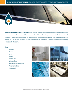
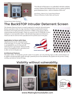


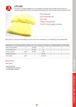


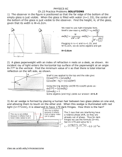

© Copyright 2026