
QUARTZ CRYSTAL RESONATORS AND OSCILLATORS A Tutorial John R. Vig
SLCET-TR-88-1 (Rev.8.4.2) AD-A328861 (revised) QUARTZ CRYSTAL RESONATORS AND OSCILLATORS For Frequency Control and Timing Applications A Tutorial John R. Vig U.S. Army Communications-Electronics Command Attn: AMSEL-RD-C2-PT Fort Monmouth, NJ 07703, USA [email protected] January 2000 Approved for public release. Distribution is unlimited. NOTICES Disclaimer The findings in this report are not to be construed as an official Department of the Army position, unless so designated by other authorized documents. The citation of trade names and names of manufacturers in this report is not to be construed as official Government endorsement or consent or approval of commercial products or services referenced herein. Report Documentation Page Table of Contents Preface………………………………..……………………….. v 1. Applications and Requirements………………………. 1 2. Quartz Crystal Oscillators………………………………. 2 3. Quartz Crystal Resonators……………………………… 3 4. Oscillator Stability………………………………………… 4 5. Quartz Material Properties……………………………... 5 6. Atomic Frequency Standards…………………………… 6 7. Oscillator Comparison and Specification…………….. 7 8. Time and Timekeeping…………………………………. 8 9. Related Devices and Applications……………………… 9 10. FCS Proceedings Ordering, Website, and Index………….. 10 iii Preface Why This Tutorial? “Everything should be made as simple as possible - but not simpler,” said Einstein. The main goal of this “tutorial” is to assist with presenting the most frequently encountered concepts in frequency control and timing, as simply as possible. I was frequently asked for “hard-copies” of the slides, so I started organizing, adding some text, and filling the gaps in the slide collection. As the collection grew, I began receiving favorable comments and requests for additional copies. Apparently, others, too, found this collection to be useful. Eventually, I assembled this document, the “Tutorial”. I have often been called upon to brief visitors, management, and potential users of precision oscillators, and have also been invited to present seminars, tutorials, and review papers before university, IEEE, and other professional groups. In the beginning, I spent a great deal of time preparing these presentations. Much of the time was spent on preparing the slides. As I accumulated more and more slides, it became easier and easier to prepare successive presentations. This is a work in progress. I plan to include new material, including additional notes. Comments, corrections, and suggestions for future revisions will be welcome. John R. Vig iv Don’t Forget the Notes! In the PowerPoint version of this document, notes and references can be found in the “Notes” of most of the pages. To view the notes, use the “Notes Page View” icon (near the lower left corner of the screen), or select “Notes Page” in the View menu. In PowerPoint 2000 (and, presumably, later versions), the notes also appear in the “Normal view”. To print a page so that it includes the notes, select Print in the File menu, and, near the bottom, at “Print what:,” select “Notes Pages”. The HTML version can be viewed with a web browser (best viewed at 1024 x 768 screen size). The notes then appear in the lower pane on the right. v CHAPTER 1 Applications and Requirements 1 Electronics Applications of Quartz Crystals Industrial Communications Telecommunications Mobile/cellular/portable radio, telephone & pager Aviation Marine Navigation Instrumentation Computers Digital systems Research & Metrology CRT displays Disk drives Atomic clocks Modems Instruments Astronomy & geodesy Tagging/identification Utilities Space tracking Sensors Celestial navigation Military & Aerospace Communications Navigation IFF Radar Sensors Guidance systems Fuzes Electronic warfare Sonobouys 1-1 Consumer Watches & clocks Cellular & cordless phones, pagers Radio & hi-fi equipment Color TV Cable TV systems Home computers VCR & video camera CB & amateur radio Toys & games Pacemakers Other medical devices Automotive Engine control, stereo, clock Trip computer, GPS Frequency Control Device Market (as of ~1997) Technology Units per year Unit price, typical Worldwide market, $/year Crystal ~ 2 x 10⁹ ~$1 ($0.1 to 3,000) ~$1.2B Hydrogen maser ~ 10 $200,000 $2M Cesium beam frequency standard Rubidium cell frequency standard ~ 300 $50,000 $15M ~ 20,000 $2,000 $40M Atomic Frequency Standards (see chapter 6) 1-2 Navigation Precise time is essential to precise navigation. Historically, navigation has been a principal motivator in man's search for better clocks. Even in ancient times, one could measure latitude by observing the stars' positions. However, to determine longitude, the problem became one of timing. Since the earth makes one revolution in 24 hours, one can determine longitude form the time difference between local time (which was determined from the sun's position) and the time at the Greenwich meridian (which was determined by a clock): Longitude in degrees = (360 degrees/24 hours) x t in hours. In 1714, the British government offered a reward of 20,000 pounds to the first person to produce a clock that allowed the determination of a ship's longitude to 30 nautical miles at the end of a six week voyage (i.e., a clock accuracy of three seconds per day). The Englishman John Harrison won the competition in 1735 for his chronometer invention. Today's electronic navigation systems still require ever greater accuracies. As electromagnetic waves travel 300 meters per microsecond, e.g., if a vessel's timing was in error by one millisecond, a navigational error of 300 kilometers would result. In the Global Positioning System (GPS), atomic clocks in the satellites and quartz oscillators in the receivers provide nanosecond-level accuracies. The resulting (worldwide) navigational accuracies are about ten meters (see chapter 8 for further details about GPS). 1-3 Commercial Two-way Radio Historically, as the number of users of commercial two-way radios have grown, channel spacings have been narrowed, and higherfrequency spectra have had to be allocated to accommodate the demand. Narrower channel spacings and higher operating frequencies necessitate tighter frequency tolerances for both the transmitters and the receivers. In 1940, when only a few thousand commercial broadcast transmitters were in use, a 500 ppm tolerance was adequate. Today, the oscillators in the many millions of cellular telephones (which operate at frequency bands above 800 MHz) must maintain a frequency tolerance of 2.5 ppm and better. The 896-901 MHz and 935-940 MHz mobile radio bands require frequency tolerances of 0.1 ppm at the base station and 1.5 ppm at the mobile station. The need to accommodate more users will continue to require higher and higher frequency accuracies. For example, a NASA concept for a personal satellite communication system would use walkie-talkie-like hand-held terminals, a 30 GHz uplink, a 20 GHz downlink, and a 10 kHz channel spacing. The terminals' frequency accuracy requirement is a few parts in 108. 1-4 Digital Processing of Analog Signals The Effect of Timing Jitter (A) Analog* input A/D A/D converter converter Digital Digital processor processor D/A D/A converter converter Analog output Digital output * e.g., from an antenna (C) (B) V(t) V(t) Time Analog signal Digitized signal 1-5 ∆V ∆t • Digital Network Synchronization Synchronization plays a critical role in digital telecommunication systems. It ensures that information transfer is performed with minimal buffer overflow or underflow events, i.e., with an acceptable level of "slips." Slips cause problems, e.g., missing lines in FAX transmission, clicks in voice transmission, loss of encryption key in secure voice transmission, and data retransmission. • In AT&T's network, for example, timing is distributed down a hierarchy of nodes. A timing source-receiver relationship is established between pairs of nodes containing clocks. The clocks are of four types, in four "stratum levels." Stratum Accuracy (Free Running) Long Term Per 1st Day Clock Type Number Used 1 1 x 10-11 N.A. GPS W/Two Rb 16 2 1.6 x 10⁻⁸ 1 x 10⁻¹⁰ Rb Or OCXO ~200 3 4.6 x 10⁻⁶ 3.7 x 10⁻⁷ OCXO Or TCXO 4 3.2 x 10⁻⁵ N.A. 1-6 XO 1000’s ~1 million Phase Noise in PLL and PSK Systems The phase noise of oscillators can lead to erroneous detection of phase transitions, i.e., to bit errors, when phase shift keyed (PSK) digital modulation is used. In digital communications, for example, where 8-phase PSK is used, the maximum phase tolerance is ±22.5o, of which ±7.5o is the typical allowable carrier noise contribution. Due to the statistical nature of phase deviations, if the RMS phase deviation is 1.5o, for example, the probability of exceeding the ±7.5o phase deviation is 6 X 10⁻⁷, which can result in a bit error rate that is significant in some applications. Shock and vibration can produce large phase deviations even in "low noise" oscillators. Moreover, when the frequency of an oscillator is multiplied by N, the phase deviations are also multiplied by N. For example, a phase deviation of 10-3 radian at 10 MHz becomes 1 radian at 10 GHz. Such large phase excursions can be catastrophic to the performance of systems, e.g., of those which rely on phase locked loops (PLL) or phase shift keying (PSK). Low noise, acceleration insensitive oscillators are essential in such applications. 1-7 Utility Fault Location Zap! ta tb Substation Substation AA Substation Substation BB Insulator Sportsman X L When a fault occurs, e.g., when a "sportsman" shoots out an insulator, a disturbance propagates down the line. The location of the fault can be determined from the differences in the times of arrival at the nearest substations: x=1/2[L - c(tb-ta)] = 1/2[L - c∆t] where x = distance of the fault from substation A, L = A to B line length, c = speed of light, and ta and tb= time of arrival of disturbance at A and B, respectively. Fault locator error = xerror=1/2(c∆terror); therefore, if ∆terror ≤ 1 microsecond, then xerror ≤ 150 meters ≤ 1/2 of high voltage tower spacings, so, the utility company can send a repair crew directly to the tower that is nearest to the fault. 1-8 Space Exploration ∆t Schematic of VBLI Technique Mean wavelength λ ∆θ ∆θ Wavefront Local Local Time & Time & Frequency Frequency Standard Standard θ(t) Microwave mixer Recorder Recorder ∆θ = Local Local Time & Time & Frequency Frequency Standard Standard Data tape Data tape Microwave mixer Recorder Recorder Correlation Correlation and and Integration Integration c∆ t Lsin θ Amplitude λ/L sin θ 1-9 θ (τ ) Angle Interference Fringes Military Requirements Military needs are a prime driver of frequency control technology. Modern military systems require oscillators/clocks that are: • Stable over a wide range of parameters (time, temperature, acceleration, radiation, etc.) • Low noise • Low power • Small size • Fast warmup • Low life-cycle cost 1-10 Impacts of Oscillator Technology Improvements • • • • • • • • • • • • • • • • Higher jamming resistance & improved ability to hide signals Improved ability to deny use of systems to unauthorized users Longer autonomy period (radio silence interval) Fast signal acquisition (net entry) Lower power for reduced battery consumption Improved spectrum utilization Improved surveillance capability (e.g., slow-moving target detection, bistatic radar) Improved missile guidance (e.g., on-board radar vs. ground radar) Improved identification-friend-or-foe (IFF) capability Improved electronic warfare capability (e.g., emitter location via TOA) Lower error rates in digital communications Improved navigation capability Improved survivability and performance in radiation environment Improved survivability and performance in high shock applications Longer life, and smaller size, weight, and cost Longer recalibration interval (lower logistics costs) 1-11 • • • • Spread Spectrum Systems In a spread spectrum system, the transmitted signal is spread over a bandwidth that is much wider than the bandwidth required to transmit the information being sent (e.g., a voice channel of a few kHz bandwidth is spread over many MHz). This is accomplished by modulating a carrier signal with the information being sent, using a wideband pseudonoise (PN) encoding signal. A spread spectrum receiver with the appropriate PN code can demodulate and extract the information being sent. Those without the PN code may completely miss the signal, or if they detect the signal, it appears to them as noise. Two of the spread spectrum modulation types are: 1. direct sequence, in which the carrier is modulated by a digital code sequence, and 2. frequency hopping, in which the carrier frequency jumps from frequency to frequency, within some predetermined set, the order of frequencies being determined by a code sequence. Transmitter and receiver contain clocks which must be synchronized; e.g., in a frequency hopping system, the transmitter and receiver must hop to the same frequency at the same time. The faster the hopping rate, the higher the jamming resistance, and the more accurate the clocks must be (see the next page for an example). Advantages of spread spectrum systems include the following capabilities: 1. rejection of intentional and unintentional jamming, 2. low probability of intercept (LPI), 3. selective addressing, 4. multiple access, and 5. high accuracy navigation and ranging. 1-12 Clock for Very Fast Frequency Hopping Radio Example Jammer J t1 Radio R1 Let R1 to R2 = 1 km, R1 to J =5 km, and J to R2 = 5 km. Then, since propagation delay =3.3 µs/km, t1 = t2 = 16.5 µs, tR = 3.3 µs, and tm < 30 µs. Allowed clock error ≈ 0.2 tm ≈ 6 µs. t2 tR Radio R2 To defeat a “perfect” follower jammer, one needs a hop-rate given by: For a 4 hour resynch interval, clock accuracy requirement is: 4 X 10⁻¹⁰ tm < (t1 + t2) - tR where tm ≈ message duration/hop ≈ 1/hop-rate 1-13 Clocks and Frequency Hopping C3 Systems Slow hopping ‹-------------------------------›Good clock Fast hopping ‹------------------------------› Better clock Extended radio silence ‹-----------------› Better clock Extended calibration interval ‹----------› Better clock Othogonality ‹-------------------------------› Better clock Interoperability ‹----------------------------› Better clock 1-14 Identification-Friend-Or-Foe (IFF) Air Defense IFF Applications AWACS FRIEND OR FOE? F-16 FAAD STINGER PATRIOT 1-15 Effect of Noise in Doppler Radar System A Transmitter Transmitter Moving Moving Object Object Decorrelated Clutter Noise Stationary Stationary Object Object Doppler Signal fD Receiver fD • Echo = Doppler-shifted echo from moving target + large "clutter" signal • (Echo signal) - (reference signal) --› Doppler shifted signal from target • Phase noise of the local oscillator modulates (decorrelates) the clutter signal, generates higher frequency clutter components, and thereby degrades the radar's ability to separate the target signal from the clutter signal. 1-16 f Bistatic Radar Conventional (i.e., "monostatic") radar, in which the Illuminator illuminator and receiver are on the same platform, is vulnerable to a variety of countermeasures. Bistatic radar, in which the illuminator and receiver are widely separated, can greatly reduce the vulnerability to countermeasures such as jamming and antiradiation weapons, and can increase slow moving target detection and identification capability via "clutter tuning” Receiver (receiver maneuvers so that its motion compensates for the motion of the illuminator; creates zero Doppler shift for the area being searched). The transmitter can remain far from the battle area, in a "sanctuary." The receiver can remain "quiet.” The timing and phase coherence problems can be orders of magnitude more severe in bistatic than in monostatic radar, especially when the platforms are moving. The Target reference oscillators must remain synchronized and syntonized during a mission so that the receiver knows when the transmitter emits each pulse, and the phase variations will be small enough to allow a satisfactory image to be formed. Low noise crystal oscillators are required for short term stability; atomic frequency standards are often required for long term stability. 1-17 Radar Frequency (GHz) 20 15 0 25 or Slow 30 Moving Vechile 40 10 100 1K 1-18 10 10K 2,400 k m/h 2 Aircra ft bsonic A ircraft - Mach 700km/h - Su 100km/ h - Veh icle, Gro und or A ir 4km/h Man Doppler Shifts X-Band RADAR 5 100K 1M Doppler Shift for Target Moving Toward Fixed Radar (Hz) CHAPTER 2 Quartz Crystal Oscillators 2 Crystal Oscillator Tuning Voltage Crystal resonator Output Frequency Amplifier 2-1 Oscillation • • • • At the frequency of oscillation, the closed loop phase shift = 2nπ. When initially energized, the only signal in the circuit is noise. That component of noise, the frequency of which satisfies the phase condition for oscillation, is propagated around the loop with increasing amplitude. The rate of increase depends on the excess; i.e., small-signal, loop gain and on the BW of the crystal in the network. The amplitude continues to increase until the amplifier gain is reduced either by nonlinearities of the active elements ("self limiting") or by some automatic level control. At steady state, the closed-loop gain = 1. 2-2 Oscillation and Stability • • • If a phase perturbation ∆φ occurs, the frequency must shift ∆f to maintain the 2nπ π phase condition, where ∆f/f=-∆φ ∆φ/2Q ∆φ L for a series-resonance oscillator, φ/df and QL is loaded Q of the crystal in the network. The "phase slope," dφ is proportional to QL in the vicinity of the series resonance frequency (also see "Equivalent Circuit" and "Frequency vs. Reactance" in Chapt. 3). Most oscillators operate at "parallel resonance," where the reactance vs. frequency slope, dX/df, i.e., the "stiffness," is inversely proportional to C1, the motional capacitance of the crystal unit. For maximum frequency stability with respect to phase (or reactance) perturbations in the oscillator loop, the phase slope (or reactance slope) must be maximum, i.e., C1 should be minimum and QL should be maximum. A quartz crystal unit's high Q and high stiffness makes it the primary frequency (and frequency stability) determining element in oscillators. 2-3 Tunability and Stability Making an oscillator tunable over a wide frequency range degrades its stability because making an oscillator susceptible to intentional tuning also makes it susceptible to factors that result in unintentional tuning. The wider the tuning range, the more difficult it is to maintain a high stability. For example, if an OCXO is designed to have a short term stability of 1 x 10-12 for some averaging time and a tunability of 1 x 10⁻⁷, then the crystal's load reactance must be stable to 1 x 10⁻⁵ for that averaging time. Achieving such stability is difficult because the load reactance is affected by stray capacitances and inductances, by the stability of the varactor's capacitance vs. voltage characteristic, and by the stability of the voltage on the varactor. Moreover, the 1 x 10⁻⁵ load reactance stability must be maintained not only under benign conditions, but also under changing environmental conditions (temperature, vibration, radiation, etc.). Whereas a high stability, ovenized 10 MHz voltage controlled oscillator may have a frequency adjustment range of 5 x 10⁻⁷ and an aging rate of 2 x 10⁻⁸ per year, a wide tuning range 10 MHz VCXO may have a tuning range of 50 ppm and an aging rate of 2 ppm per year. 2-4 Oscillator Acronyms • XO…………..Crystal Oscillator • VCXO………Voltage Controlled Crystal Oscillator • OCXO………Oven Controlled Crystal Oscillator • TCXO………Temperature Compensated Crystal Oscillator • TCVCXO..…Temperature Compensated/Voltage Controlled Crystal Oscillator • OCVCXO.….Oven Controlled/Voltage Controlled Crystal Oscillator • MCXO………Microcomputer Compensated Crystal Oscillator • RbXO……….Rubidium-Crystal Oscillator 2-5 Crystal Oscillator Categories The three categories, based on the method of dealing with the crystal unit's frequency vs. temperature (f vs. T) characteristic, are: • • • XO, crystal oscillator, does not contain means for reducing the crystal's f vs. T characteristic (also called PXO-packaged crystal oscillator). TCXO, temperature compensated crystal oscillator, in which, e.g., the output signal from a temperature sensor (e.g., a thermistor) is used to generate a correction voltage that is applied to a variable reactance (e.g., a varactor) in the crystal network. The reactance variations compensate for the crystal's f vs. T characteristic. Analog TCXO's can provide about a 20X improvement over the crystal's f vs. T variation. OCXO, oven controlled crystal oscillator, in which the crystal and other temperature sensitive components are in a stable oven which is adjusted to the temperature where the crystal's f vs. T has zero slope. OCXO's can provide a >1000X improvement over the crystal's f vs. T variation. 2-6 Crystal Oscillator Categories ∆f f +10 ppm 250C Voltage Tune +1000C -450C Output T • Crystal Oscillator (XO) Temperature Temperature Sensor Sensor Compensation Compensation Network or Network or Computer Computer -10 ppm -450C ∆f f +1 ppm +1000C T XO XO -1 ppm • Temperature Compensated (TCXO) Oven Oven Oven control control XO XO Temperature Temperature Sensor Sensor -450C ∆f f +1 x 10⁻⁸ +1000C T -1 x 10⁻⁸ • Oven Controlled (OCXO) 2-7 Hierarchy of Oscillators Oscillator Type* • Crystal oscillator (XO) • Temperature compensated Accuracy** Typical Applications 10-5 to 10-4 Computer timing 10-6 Frequency control in tactical radios 10-8 to 10-7 Spread spectrum system clock 10-8 (with 10-10 per g option) Navigation system clock & frequency standard, MTI radar • Small atomic frequency 10-9 C3 satellite terminals, bistatic, & multistatic radar • High performance atomic 10-12 to 10-11 Strategic C3, EW crystal oscillator (TCXO) • Microcomputer compensated crystal oscillator (MCXO) • Oven controlled crystal oscillator (OCXO) standard (Rb, RbXO) standard (Cs) * Sizes range from <5cm3 for clock oscillators to > 30 liters for Cs standards Costs range from <$5 for clock oscillators to > $50,000 for Cs standards. ** Including environmental effects (e.g., -40oC to +75oC) and one year of aging. 2-8 Oscillator Circuit Types Of the numerous oscillator circuit types, three of the more common ones, the Pierce, the Colpitts and the Clapp, consist of the same circuit except that the rf ground points are at different locations. The Butler and modified Butler are also similar to each other; in each, the emitter current is the crystal current. The gate oscillator is a Pierce-type that uses a logic gate plus a resistor in place of the transistor in the Pierce oscillator. (Some gate oscillators use more than one gate). b c ∈ Pierce c ∈ ∈ b ∈ c b Colpitts b c Clapp c ∈ b Butler Modified Butler 2-9 Gate OCXO Block Diagram ϕ Output Oven Each of the three main parts of an OCXO, i.e., the crystal, the sustaining circuit, and the oven, contribute to instabilities. The various instabilities are discussed in the rest of chapter 3 and in chapter 4. 2-10 Oscillator Instabilities - General Expression ∆f foscillator ≈ ∆f fresonator 1 + 2QL 2ff QL 1 + f 2 −1/2 dφ(ff ) where QL = loaded Q of the resonator, and dφ(ff) is a small change in loop phase at offset frequency ff away from carrier frequency f. Systematic phase changes and phase noise within the loop can originate in either the resonator or the sustaining circuits. Maximizing QL helps to reduce the effects of noise and environmentally induced changes in the sustaining electronics. In a properly designed oscillator, the short-term instabilities are determined by the resonator at offset frequencies smaller than the resonator’s half-bandwidth, and by the sustaining circuit and the amount of power delivered from the loop for larger offsets. 2-11 Instabilities due to Sustaining Circuit • Load reactance change - adding a load capacitance to a crystal changes the frequency by C1 ∆ f ≅ δf≡ f 2(C0 + CL ) then, ∆ (δ f ) C1 ≅− 2 ∆ CL 2(C0 + CL ) • Example: If C0 = 5 pF, C1 = 14fF and CL = 20pF, then a ∆CL = 10 fF (= 5 X 10⁻⁴) causes ≈1 X 10⁻⁷ frequency change, and a CL aging of 10 ppm per day causes 2 X 10⁻⁹ per day of oscillator aging. • Drive level changes: Typically 10-8 per ma2 for a 10 MHz 3rd SC-cut. • DC bias on the crystal also contributes to oscillator aging. 2-12 Oscillator Instabilities - Tuned Circuits Many oscillators contain tuned circuits - to suppress unwanted modes, as matching circuits, and as filters. The effects of small changes in the tuned circuit's inductance and capacitance is given by: ∆f f oscillator dφ (ff ) 1 ≈ ≈ 2QL 1 + 2ff BW Q dC dL c c + c L Q Cc c where BW is the bandwidth of the filter, ff is the frequency offset of the center frequency of the filter from the carrier frequency, QL is the loaded Q of the resonator, and Qc, Lc and Cc are the tuned circuit's Q, inductance and capacitance, respectively. 2-13 Oscillator Instabilities - Circuit Noise Flicker PM noise in the sustaining circuit causes flicker FM contribution to the oscillator output frequency given by: 2 f L osc (ff ) = L ckt (1Hz ) 3 2 4ff QL and 1 σ y (τ) = ln2 L ckt (1Hz ) QL where ff is the frequency offset from the carrier frequency f, QLis the loaded Q of the resonator in the circuit, Lckt (1Hz) is the flicker PM noise at ff = 1Hz, and τ is any measurement time in the flicker floor range. For QL = 106 and Lckt (1Hz) = -140dBc/Hz, σy(τ) = 8.3 x 10⁻¹⁴. ( Lckt (1Hz) = -155dBc/Hz has been achieved.) 2-14 Oscillator Instabilities - External Load If the external load changes, there is a change in the amplitude or phase of the signal reflected back into the oscillator. The portion of that signal which reaches the oscillating loop changes the oscillation phase, and hence the frequency by ∆f dφ(ff ) 1 Γ − 1 ≈ ≈ (sinθ ) isolation f oscillator 2Q 2Q Γ + 1 where Γ is the VSWR of the load, and θ is the phase angle of the reflected wave; e.g., if Q ~ 106, and isolation ~40 dB (i.e., ~10-4), then the worst case (100% reflection) pulling is ~5 x 10⁻⁹. A VSWR of 2 reduces the maximum pulling by only a factor of 3. The problem of load pulling becomes worse at higher frequencies, because both the Q and the isolation are lower. 2-15 Oscillator Outputs Most users require a sine wave, a TTL-compatible, a CMOScompatible, or an ECL-compatible output. The latter three can be simply generated from a sine wave. The four output types are illustrated below, with the dashed lines representing the supply voltage inputs, and the bold solid lines, the outputs. (There is no “standard” input voltage for sine wave oscillators, and the input voltage for CMOS typically ranges from 3V to 15V.) +15V +10V +5V 0V -5V Sine TTL CMOS 2-16 ECL Resonator Self-Temperature Sensing fβ ≡ 3f1 - f3 fβ (Hz) 172300 dfβ = − 14 Hz/oC dT 171300 -35 -15 5 25 170300 2-17 45 65 85 Temperature (oC) Thermometric Beat Frequency Generation DUAL MODE OSCILLATOR f1 X3 X3 MULTIPLIER MULTIPLIER M=1 Mixer M=3 f3 2-18 fβ = 3f1 - f3 LOW PASS LOW PASS FILTER FILTER Microcomputer Compensated Crystal Oscillator (MCXO) f1 DualDualmode mode XO XO x3 x3 fβ f3 Reciprocal Reciprocal Counter Counter N1 Mixer 2-19 µµcomcomputer puter N2 Correction Correction Circuit Circuit f0 MCXO Frequency Summing Method Block Diagram VCXO 3rd OVERTONE CRYSTAL f3 = 10 MHz fd DUAL-MODE OSCILLATOR FUNDAMENTAL MODE fd F f1 Divide by 2500 TClock DIRECT DIGITAL SYNTHESIZER fb Clock Clock N1 out 10 MHz output LOCKED LOOP Divide by 3 Mixer COUNTER PHASE- MICROCOMPUTER N2 T F Divide by 4000 NON-VOLATILE MEMORY T = Timing Mode F = Frequency Mode 2-20 1 PPS output MCXO - Pulse Deletion Method fc f Dual Dualmode mode β oscillator oscillator Digital circuitry (ASIC) output output Pulse Pulse eliminator eliminator Counter Counter SC-cut crystal Frequency Frequency evaluator evaluator &&correction correction determination determination f0 corrected output for timing Microprocessor circuitry Microcomputer compensated crystal oscillator (MCXO) block diagram - pulse deletion method. 2-21 MCXO - TCXO Resonator Comparison Parameter MCXO Cut, overtone TCXO SC-cut, 3rd AT-cut, fund. Angle-of-cut tolerance Loose Tight Blank f and plating tolerance Loose Tight Low Significant Hysteresis (-550C to +850C) 10-9 to 10-8 10-7 to 10-6 Aging per year 10-8 to 10-7 10-7 to 10-6 Activity dip incidence 2-22 Opto-Electronic Oscillator (OEO) Bias "Pump Laser" Optical out Piezoelectric fiber stretcher RF driving port Electrical output Electrical injection Filter Optical Fiber RF coupler RF Amplifier Photodetector Optical Injection Optical fiber Optical coupler Electrical transmission line 2-23 CHAPTER 3 Quartz Crystal Resonators 3 Why Quartz? Quartz is the only material known that possesses the following combination of properties: • Piezoelectric ("pressure-electric"; piezein = to press, in Greek) • Zero temperature coefficient cuts exist • Stress compensated cut exists • Low loss (i.e., high Q) • Easy to process; low solubility in everything, under "normal" conditions, except the fluoride etchants; hard but not brittle • Abundant in nature; easy to grow in large quantities, at low cost, and with relatively high purity and perfection. Of the man-grown single crystals, quartz, at ~3,000 tons per year, is second only to silicon in quantity grown (3 to 4 times as much Si is grown annually, as of 1997). 3-1 The Piezoelectric Effect Y Y _ + + _ _ _ _ + + + + + _ _ + • • + + _ + _ + Undeformed lattice + + + X + _ _ _ + _ + _ + _ _ _ + + _ + + _ - _ + + _ X _ _ _ + _ _ _ + _ _ _ + + + + + _ _ _ _ + + + + + + _ _ _ _ + + + + _ _ _ _ _ + Strained lattice The piezoelectric effect provides a coupling between the mechanical properties of a piezoelectric crystal and an electrical circuit. 3-2 The Piezoelectric Effect in Quartz Z FIELD along: STRAIN X X EXTENSIONAL along: Y Y √ √ X Z X SHEAR about: Z √ Y √ Z √ Y In quartz, the five strain components shown may be generated by an electric field. The modes shown on the next page may be excited by suitably placed and shaped electrodes. The shear strain about the Z-axis produced by the Y-component of the field is used in the rotated Y-cut family, including the AT, BT, and ST-cuts. 3-3 Modes of Motion Flexure Mode Extensional Mode Face Shear Mode Thickness Shear Fundamental Mode Third Overtone Thickness Shear Thickness Shear Mode 3-4 Resonator Vibration Amplitude Distribution Metallic electrodes Resonator plate substrate (the “blank”) u Conventional resonator geometry and amplitude distribution, u 3-5 Resonant Vibrations of a Quartz Plate 3555 3200 MHZ 3507 -10 db. 3383 3742 -20 3852 3802 3707 3652 3642 -30 db. 3256 Response 0 db. -40 db. 3200 3400 3600 3800 Frequency, in kHz X-ray topographs (21•0 plane) of various modes excited during a frequency scan of a fundamental mode, circular, AT-cut resonator. The first peak, at 3.2 MHz, is the main mode; all others are unwanted modes. Dark areas correspond to high amplitudes of displacement. 3-6 Overtone Response of a Quartz Crystal Reactance jX Spurious responses Spurious responses Spurious responses 0 Frequency 5th overtone -jX 3rd overtone Fundamental mode 3-7 Unwanted Modes vs. Temperature (3 MHz rectangular AT-cut resonator, 22 X 27 X 0.552 mm) Activity dips occur where the f vs. T curves of unwanted modes intersect the f vs. T curve of the wanted mode. Such activity dips are highly sensitive to drive level and load reactance. 3-8 Mathematical Description of a Quartz Resonator • In piezoelectric materials, electrical current and voltage are coupled to elastic displacement and stress: {T} = [C] {S} - [e] {E} {D} = [e] {S} + [∈ ∈] {E} where {T} = stress tensor, [C] = elastic stiffness matrix, {S} = strain tensor, [e] = piezoelectric matrix {E} = electric field vector, {D} = electric displacement vector, and [∈ ∈] = is the dielectric matrix • For a linear piezoelectric material T1 T2 T3 T4 T5 T6 D1 D2 D3 = C11 C21 C31 C41 C51 C61 C12 C22 C32 C42 C52 C62 C13 C23 C33 C43 C53 C63 C14 C24 C34 C44 C54 C64 C15 C25 C35 C45 C55 C65 C16 −e11 C26 −e12 C36 −e13 C46 −e14 C56 −e15 C66 −e16 −e21 −e31 −e22 −e32 −e23 −e33 −e24 −e34 −e25 −e35 −e26 −e36 e11 e12 e13 e14 e15 e16 ∈11 ∈12 ∈13 e21 e22 e23 e24 e25 e26 ∈21 ∈22 ∈23 e31 e32 e33 e34 e35 e36 ∈31 ∈32 ∈33 S1 S2 S3 S4 S5 , S6 E1 E2 E3 • Elasto-electric matrix for quartz S1 S2 S3 S4 S5 S6 -E1 -E2 -E3 T1 et T2 T3 T4 T5 T6 CE X D1 where T1 = T11, T2 = T22, T3 = T33, T4 = T23, T5 = T13, T6 = T12, D2 S1 = S11, S2 = S22, S3 = S33, S4 = 2S23, S5 = 2S13, S6 = 2S12, D3 e ∈ S LINES JOIN NUMERICAL EQUALITIES EXCEPT FOR COMPLETE RECIPROCITY ACROSS PRINCIPAL DIAGONAL INDICATES NEGATIVE OF INDICATES TWICE THE NUMERICAL EQUALITIES X INDICATES 1/2 (c11 - c12) 3-9 6 2 2 10 Mathematical Description - Continued • Number of independent non-zero constants depend on crystal symmetry. For quartz (trigonal, class 32), there are 10 independent linear constants - 6 elastic, 2 piezoelectric and 2 dielectric. "Constants” depend on temperature, stress, coordinate system, etc. • To describe the behavior of a resonator, the differential equations for Newton's law of motion for a continuum, and for Maxwell's equation* must be solved, with the proper electrical and mechanical boundary conditions at the plate surfaces. ∂Tij ∂Di Ei ∂φ =− ; S = ij ∂x i 1 ∂ui 2 ( ∂x j (F = ma ⇒ + ∂u j ∂xi ) ; etc.) ∂xj &&i ; =ρu ∇ ⋅D = 0 ⇒ ∂xi = 0, • Equations are very "messy" - they have never been solved in closed form for physically realizable threedimensional resonators. Nearly all theoretical work has used approximations. • Some of the most important resonator phenomena (e.g., acceleration sensitivity) are due to nonlinear effects. Quartz has numerous higher order constants, e.g., 14 third-order and 23 fourth-order elastic constants, as well as 16 third-order piezoelectric coefficients are known; nonlinear equations are extremely messy. * Magnetic field effects are generally negligible; quartz is diamagnetic, however, magnetic fields can affect the mounting structure and electrodes. 3-10 Infinite Plate Thickness Shear Resonator n c ij fn = , n = 1, 3, 5... 2h ρ Where fn = resonant frequency of n-th harmonic h = plate thickness ρ = density cij = elastic modulus associated with the elastic wave being propagated d(log fn ) 1 dfn − 1 dh 1 dρ 1 dc ij Tf = = = − + dT fn dT h dT 2ρ dT 2c ij dT where Tf is the linear temperature coefficient of frequency. The temperature coefficient of cij is negative for most materials (i.e., “springs” become “softer” as T increases). The coefficients for quartz can be +, - or zero (see next page). 3-11 Quartz is Highly Anisotropic The properties of quartz vary greatly with crystallographic direction. For example, when a quartz sphere is etched deeply in HF, the sphere takes on a triangular shape when viewed along the Z-axis, and a lenticular shape when viewed along the Y-axis. The etching rate is more than 100 times faster along the fastest etching rate direction (the Z-direction) than along the slowest direction (the slow-X-direction). The thermal expansion coefficient is 7.8 x 10⁻⁶/°C along the Zdirection, and 14.3 x 10⁻⁶/°C perpendicular to the Z-direction; the temperature coefficient of density is, therefore, -36.4 x 10⁻⁶/°C. The temperature coefficients of the elastic constants range from -3300 x 10-6/°C (for C12) to +164 x 10-6/°C (for C66). For the proper angles of cut, the sum of the first two terms in Tf on the previous page is cancelled by the third term, i.e., temperature compensated cuts exist in quartz. (See next page.) 3-12 Zero Temperature Coefficient Quartz Cuts 90o 60o AT 30o θ z FC IT SC LC 0 SBTC -30o BT -60o -90o θ g ly d n i S t a te Ro t Cu Do ub Ro ly ta t Cu e d t 0o θ y 10o 30o The AT, FC, IT, SC, BT, and SBTC-cuts are some of the cuts on the locus of zero temperature coefficient cuts. The LC is a “linear coefficient” cut that has been used in a quartz thermometer. φ x φ 20o Y-cut: ≈ +90 ppm/0C (thickness-shear mode) xl X-cut: ≈ -20 ppm/0C (extensional mode) 3-13 Comparison of SC and AT-cuts • Advantages of the SC-cut • Thermal transient compensated (allows faster warmup OCXO) • Static and dynamic f vs. T allow higher stability OCXO and MCXO • Better f vs. T repeatability allows higher stability OCXO and MCXO • Far fewer activity dips • Lower drive level sensitivity • Planar stress compensated; lower ∆f due to edge forces and bending • Lower sensitivity to radiation • Higher capacitance ratio (less ∆f for oscillator reactance changes) • Higher Q for fundamental mode resonators of similar geometry • Less sensitive to plate geometry - can use wide range of contours • Disadvantage of the SC-cut : More difficult to manufacture for OCXO (but is easier to manufacture for MCXO than is an AT-cut for precision TCXO) • Other Significant Differences • B-mode is excited in the SC-cut, although not necessarily in LFR's • The SC-cut is sensitive to electric fields (which can be used for compensation) 3-14 Mode Spectrograph of an SC-cut 1.10 0 1.0 1.88 -10 Attenuation a-mode: quasi-longitudinal mode b-mode: fast quasi-shear mode c-mode: slow quasi-shear mode 3.30 -20 3.0 5.50 -30 5.0 c(1) -40 5.65 0 b(1) 1 a(1) 2 c(3) b(3) 3 c(5) 4 b(5) 5 Normalized Frequency (referenced to the fundamental c-mode) 3-15 a(3) 6 SC- cut f vs. T for b-mode and c-mode 400 FREQUENCY DEVIATION (PPM) 200 0 10 Temperature (OC) 20 0 40 30 50 60 70 c-Mode (Slow Shear) -200 -400 b-Mode (Fast Shear) -25.5 ppm/oC -600 -800 -1000 -1200 3-16 Singly Rotated and Doubly Rotated Cuts’ Vibrational Displacements Z θ g ly Sin ated t Ro t Cu Do u Ro bly ta Cu ted t θ Y ϕ X X’ 3-17 Resonator Packaging Two-point Mount Package Quartz blank Three- and Four-point Mount Package Electrodes Quartz blank Bonding area Cover Mounting clips Seal Base Bonding area Cover Mounting clips Seal Pins Top view of cover 3-18 Pins Base Equivalent Circuits Spring C Mass L Dashpot R 3-19 Equivalent Circuit of a Resonator CL Symbol for crystal unit C0 CL C1 L1 R1 ∆f C1 ≈ → fS 2(C0 + CL ) 3-20 1. Voltage control (VCXO) 2. Temperature compensation (TCXO) Crystal Oscillator f vs. T Compensation Frequency / Voltage Uncompensated frequency T Compensating voltage on varactor CL Compensated frequency of TCXO 3-21 Resonator Frequency vs. Reactance Antiresonance Reactance Area of usual + “parallel” resonance” fS 0 Frequency Series resonance - fA 1 2πfC0 3-22 Equivalent Circuit Parameter Relationships C0 ≅ ε 1 fs = 2π A t r≡ fs fa − fs ≅ 2r 1 L1C1 1 Q= 2π fSR1C1 ϕ= τ 1 = R1C1 ≅ 10 s −14 r' C C1n ≈ 311 n C0 C1 L1n ω L1 − 1 ω C1 R1 dϕ 360 Q ≅ df π fs n3L11 ≈ 3 r' R1n 3-23 n: C 0: C 1: C1n: L1: L1n: R 1: R1n: ε: A: t: r: r’: fs: fa: Q; τ1: ω: ϕ: k; n3R11 ≈ r' Overtone number Static capacitance Motional capacitance C1 of n-th overtone Motional inductance L1 of n-th overtone Motional resistance R1 of n-th overtone Dielectric permittivity of quartz ≈40 x 10-13 pF/mm (average) Electrode area Plate thickness Capacitance ratio f1/fn Series resonance frequency ≈fR Antiresonance frequency Quality factor Motional time constant Angular frequency = 2πf Phase angle of the impedance Piezoelectric coupling factor =8.8% for AT-cut, 4.99% for SC π n 2r = 2k 2 What is Q and Why is it Important? Q ≡ 2π Energy stored during a cycle Energy lost during the cycle Q is proportional to the decay-time, and is inversely proportional to the linewidth of resonance (see next page). • The higher the Q, the higher the frequency stability and accuracy capability of a resonator (i.e., high Q is a necessary but not a sufficient condition). If, e.g., Q = 106, then 10-10 accuracy requires ability to determine center of resonance curve to 0.01% of the linewidth, and stability (for some averaging time) of 10-12 requires ability to stay near peak of resonance curve to 10-6 of linewidth. • Phase noise close to the carrier has an especially strong dependence on Q (L(f) ∝ 1/Q4). 3-24 Decay Time, Linewidth, and Q Decaying oscillation of a resonator Oscillation 1 e = 1 of maximum intensity 2.7 TIME Exciting pulse ends Max. intensity td Maximum intensity ½ Maximum intensity BW Q= ν0 νo ≅ νo π t d BW FREQUENCY 3-25 1 BW ≅ πt d Resonance behavior of a resonator Factors that Determine Resonator Q The maximum Q of a resonator can be expressed as: 1 , Q max = 2π fτ where f is the frequency in Hz, and τ is an empirically determined “motional time constant” in seconds, which varies with the angles of cut and the mode of vibration. For example, τ = 1 x 10-14s for the AT-cut's c-mode (Qmax = 3.2 million at 5 MHz), τ = 9.9 x 10⁻¹⁵s for the SC-cut's c-mode, and τ = 4.9 x 10⁻¹⁵s for the BT-cut's b-mode. Other factors which affect the Q of a resonator include: Blank geometry (contour, dimensional ratios) Drive level Gases inside the enclosure (pressure, type of gas) Interfering modes Ionizing radiation Overtone Surface finish Material impurities and defects Mounting stresses Bonding stresses Temperature Electrode geometry and type 3-26 Resonator Fabrication Steps DESIGN RESONATORS GROW QUARTZ SWEEP CUT LAP ROUND ORIENT IN MASK CLEAN ETCH (CHEMICAL POLISH) CONTOUR ANGLE CORRECT X-RAY ORIENT DEPOSIT CONTACTS PREPARE ENCLOSURE MOUNT BOND INSPECT CLEAN SEAL FREQUENCY ADJUST PLATE BAKE FINAL CLEAN TEST OSCILLATOR 3-27 X-ray Orientation of Crystal Plates Shielding Monochromator crystal Detector S X-ray beam Crystal under test Copper target X-ray source Goniometer Double-crystal x-ray diffraction system 3-28 Contamination Control Contamination control is essential during the fabrication of resonators because contamination can adversely affect: • Stability (see chapter 4) - aging - hysteresis - retrace - noise - nonlinearities and resistance anomalies (high starting resistance, second-level of drive, intermodulation in filters) - frequency jumps? • • Manufacturing yields Reliability 3-29 Crystal Enclosure Contamination The enclosure and sealing process can have important influences on resonator stability. • A monolayer of adsorbed contamination contains ~ 1015 molecules/cm2 (on a smooth surface) • An enclosure at 10-7 torr contains ~109 gaseous molecules/cm3 Therefore: In a 1 cm3 enclosure that has a monolayer of contamination on its inside surfaces, there are ~106 times more adsorbed molecules than gaseous molecules when the enclosure is sealed at 10-7 torr. The desorption and adsorption of such adsorbed molecules leads to aging, hysteresis, noise, etc. 3-30 What is an “f-squared”? It is standard practice to express the thickness removed by lapping, etching and polishing, and the mass added by the electrodes, in terms of frequency change, ∆f, in units of “f2”, where the ∆f is in kHz and f is in MHz. For example, etching a 10MHz AT-cut plate 1f2 means that a thickness is removed that produces ∆f= 100 kHz; and etching a 30 MHz plate 1f2 means that the ∆f= 900 kHz. In both cases, ∆f=1f2 produces the same thickness change. To understand this, consider that for a thickness-shear resonator (AT-cut, SC-cut, etc.) f= N t where f is the fundamental mode frequency, t is the thickness of the resonator plate and N is the frequency constant (1661 MHz•µm for an AT-cut, and 1797 MHz•µm for a SC-cut’s cmode). Therefore, ∆f ∆t =− f t and, ∆t = −N ∆f f2 So, for example, ∆f = 1f2 corresponds to the same thickness removal for all frequencies. For an AT-cut, ∆t=1.661 µm of quartz (=0.83 µm per side) per f2. An important advantage of using units of f2 is that frequency changes can be measured much more accurately than thickness changes. The reason for expressing ∆f in kHz and f in MHz is that by doing so, the numbers of f2 are typically in the range of 0.1 to 10, rather than some very small numbers. 3-31 Milestones in Quartz Technology 1880 1905 1917 1918 1926 1927 1927 1934 1949 1956 1956 1972 1974 1982 Piezoelectric effect discovered by Jacques and Pierre Curie First hydrothermal growth of quartz in a laboratory - by G. Spezia First application of piezoelectric effect, in sonar First use of piezoelectric crystal in an oscillator First quartz crystal controlled broadcast station First temperature compensated quartz cut discovered First quartz crystal clock built First practical temp. compensated cut, the AT-cut, developed Contoured, high-Q, high stability AT-cuts developed First commercially grown cultured quartz available First TCXO described Miniature quartz tuning fork developed; quartz watches available The SC-cut (and TS/TTC-cut) predicted; verified in 1976 First MCXO with dual c-mode self-temperature sensing 3-32 Quartz Resonators for Wristwatches Requirements: • Small size • Low power dissipation (including the oscillator) • Low cost • High stability (temperature, aging, shock, attitude) These requirements can be met with 32,768 Hz quartz tuning forks 3-33 Why 32,768 Hz? 32,768 = 215 • In an analog watch, a stepping motor receives one impulse per second which advances the second hand by 6o, i.e., 1/60th of a circle, every second. • Dividing 32,768 Hz by two 15 times results in 1 Hz. • The 32,768 Hz is a compromise among size, power requirement (i.e., battery life) and stability. 3-34 32,768 16,384 8,192 4,096 2,048 1,024 512 256 128 64 32 16 8 4 2 1 Quartz Tuning Fork Z Y X a) natural faces and crystallographic axes of quartz Z Y’ 0~50 Y arm base X b) crystallographic orientation of tuning fork 3-35 c) vibration mode of tuning fork Watch Crystal 3-36 Lateral Field Resonator Lateral Field Thickness Field In lateral field resonators (LFR): 1. the electrodes are absent from the regions of greatest motion, and 2. varying the orientation of the gap between the electrodes varies certain important resonator properties. Advantages of LFR are: • Ability to eliminate undesired modes, e.g., the b-mode in SC-cuts • Potentially higher Q (less damping due to electrodes and mode traps) • Potentially higher stability (less electrode and mode trap effects, smaller C1) 3-37 Electrodeless (BVA) Resonator C D2 C D1 Quartz bridge Side view of BVA2 resonator construction Side and top views of center plate C 3-38 CHAPTER 4 Oscillator Stability 4 The Units of Stability in Perspective • What is one part in 1010 ? (As in 1 x 10⁻¹⁰/day aging.) • ~1/2 cm out of the circumference of the earth. • ~1/4 second per human lifetime (of ~80 years). • What is -170 dB? (As in -170 dBc/Hz phase noise.) • -170 dB = 1 part in 1017 ≈ thickness of a sheet of paper out of total distance traveled by all the cars in the world in a day. 4-1 Accuracy, Precision, and Stability f Accurate but not precise Not accurate and not precise Precise but not accurate f f Accurate and precise f 0 Time Stable but not accurate Time Time Accurate but not stable Not stable and not accurate 4-2 Time Stable and accurate Influences on Oscillator Frequency Time • Short term (noise) • Intermediate term (e.g., due to oven fluctuations) • Long term (aging) Temperature • Static frequency vs. temperature • Dynamic frequency vs. temperature (warmup, thermal shock) • Thermal history ("hysteresis," "retrace") Acceleration • Gravity (2g tipover) • Vibration • Acoustic noise • Shock Ionizing radiation • Steady state • Pulsed • Photons (X-rays, γ-rays) • Particles (neutrons, protons, electrons) Other • Power supply voltage • Atmospheric pressure (altitude) • Humidity • Load impedance 4-3 • Magnetic field Idealized Frequency-Time-Influence Behavior ∆f X 108 f 3 Temperature Step Vibration Shock Oscillator Turn Off 2-g & Tipover Turn On Radiation Off 2 Aging 1 0 -1 On -2 Short-Term Instability -3 t0 t1 t2 t3 t4 4-4 t5 t6 t7 t8 Time Aging and Short-Term Stability Short-term instability (Noise) 30 ∆f/f (ppm) 25 20 15 10 5 10 15 20 4-5 25 Time (days) Aging Mechanisms Mass transfer due to contamination Since f ∝ 1/t, ∆f/f = -∆t/t; e.g., f5MHz ≈ 106 molecular layers, therefore, 1 quartz-equivalent monolayer ⇒ ∆f/f ≈ 1 ppm Stress relief in the resonator's: mounting and bonding structure, electrodes, and in the quartz (?) Other effects Quartz outgassing Diffusion effects Chemical reaction effects Pressure changes in resonator enclosure (leaks and outgassing) Oscillator circuit aging (load reactance and drive level changes) Electric field changes (doubly rotated crystals only) Oven-control circuitry aging 4-6 Typical Aging Behaviors A(t) = 5 ln(0.5t+1) ∆f/f Time A(t) +B(t) B(t) = -35 ln(0.006t+1) 4-7 Stresses on a Quartz Resonator Plate Causes: • Thermal expansion coefficient differences • Bonding materials changing dimensions upon solidifying/curing • Residual stresses due to clip forming and welding operations, sealing • Intrinsic stresses in electrodes • Nonuniform growth, impurities & other defects during quartz growing • Surface damage due to cutting, lapping and (mechanical) polishing Effects: • In-plane diametric forces • Tangential (torsional) forces, especially in 3 and 4-point mounts • Bending (flexural) forces, e.g., due to clip misalignment and electrode stresses • Localized stresses in the quartz lattice due to dislocations, inclusions, other impurities, and surface damage 4-8 Thermal Expansion Coefficient, α, of AT-cut Quartz, 10-6/0K Thermal Expansion Coefficients of Quartz 14 ZZl 13.71 Ψ 13 XXl Radial 12 11.63 α (Thickness) = 11.64 11 10 Tangential 9.56 9 00 100 200 300 400 500 600 Orientation, Ψ, With Respect To XXl 4-9 700 800 900 Force-Frequency Coefficient 30 * 10-15 m • s / N AT-cut quartz 25 20 15 Z’ F 10 Ψ Kf (Ψ Ψ) 5 X’ F 0 -5 -10 -15 0 0 (Force ) (Frequency constant ) ∆f = KF (Diameter ) (Thickness ) f 100 200 300 400 4-10 Ψ 500 600 700 800 900 Strains Due To Mounting Clips X-ray topograph of an AT-cut, two-point mounted resonator. The topograph shows the lattice deformation due to the stresses caused by the mounting clips. 4-11 Strains Due To Bonding Cements (a) (b) X-ray topographs showing lattice distortions caused by bonding cements; (a) Bakelite cement - expanded upon curing, (b) DuPont 5504 cement - shrank upon curing 4-12 Mounting Force Induced Frequency Change The force-frequency coefficient, KF (ψ), is defined by Z’ ( Force) (Frequency − constant ) ∆f = KF (Diameter ) (Thickness) f F Ψ Maximum KF (AT-cut) = 24.5 x 10⁻¹⁵ m-s/N at ψ = 0o Maximum KF (SC-cut) = 14.7 x 10⁻¹⁵ m-s/N at ψ = 44o F As an example, consider a 5 MHz 3rd overtone, 14 mm diameter resonator. Assuming the presence of diametrical forces only, (1 gram = 9.81 x 10⁻³ newtons), -8 ∆f = 2.9 x 10 -8 per gram for an AT-cut resonator 1.7 x 10 per gram for an SC-cut resonator f Max ∆f = 0 at ψ = 61o for an AT-cut resonator, and at ψ = 82o for an f Min { SC-cut. 4-13 X’ Apparent angle shift (minutes) Bonding Strains Induced Frequency Changes 6’ 5’ • Blank No. 7 • • Z’ Blank No. 8 4’ Ψ 3’ X’ • 2’ • 1’ • 0’ • -1’ • • -2’ 300 600 Bonding orientation, Ψ 900 When 22 MHz fundamental mode AT-cut resonators were reprocessed so as to vary the bonding orientations, the frequency vs. temperature characteristics of the resonators changed as if the angles of cut had been changed. The resonator blanks were 6.4 mm in diameter plano-plano, and were bonded to low-stress mounting clips by nickel electrobonding. 4-14 Bending Force vs. Frequency Change AT-cut resonator SC-cut resonator fo = 10Mz fo = 10Mz 5gf • • • • • • • • • 20 • +10 • • • • • • • • • 10 • 5gf Frequency Change (Hz) Frequency Change (Hz) 30 • • • • • • •• • • • • • • • • •• •• • • • • • • • • • • ••• • 360 • 60 120• 180 240 • •300 • •• • •• • Azimuth angle ψ (degrees) • • •• -10 0 60 120 180 240 300 Azimuth angle ψ (degrees) 360 Frequency change for symmetrical bending, AT-cut crystal. Frequency change for symmetrical bending, SC-cut crystal. 4-15 Short Term Instability (Noise) Stable Frequency (Ideal Oscillator) V 1 -1 T1 1 V -1 T1 Φ(t) T3 T2 V(t) = V0 sin(2πν0t) Φ(t) = 2πν0t Time Unstable Frequency (Real Oscillator) Φ(t) T2 T3 Time Φ(t) = 2πν0t + φ(t) V(t) =[V0 + ε(t)] sin[2πν0t + φ(t)] Instantaneous frequency, ν(t ) = 1 d Φ(t ) 1 dφ(t ) = ν0 + 2π d t 2π d t V(t) = Oscillator output voltage, V0 = Nominal peak voltage amplitude ε(t) = Amplitude noise, ν0 = Nominal (or "carrier") frequency Φ(t) = Instantaneous phase, and φ(t) = Deviation of phase from nominal (i.e., the ideal) 4-16 Instantaneous Output Voltage of an Oscillator - Voltage + 0 Amplitude instability Phase instability Frequency instability Time 4-17 Time Domain - Frequency Domain A f (a) Amplitude - Time Amplitude - Frequency t (b) (c) A(f) A(t) 4-18 Causes of Short Term Instabilities Johnson noise (thermally induced charge fluctuations, i.e., "thermal emf” in resistive elements) Phonon scattering by defects & quantum fluctuations (related to Q) Noise due to oscillator circuitry (active and passive components) Temperature fluctuations- thermal transient effects - activity dips at oven set-point Random vibration Fluctuations in the number of adsorbed molecules Stress relief, fluctuations at interfaces (quartz, electrode, mount, bond) Shot noise in atomic frequency standards ??? 4-19 Short-Term Stability Measures Measure Symbol Two-sample deviation, also called “Allan deviation” Spectral density of phase deviations Spectral density of fractional frequency deviations Phase noise σy(τ)* Sφ(f) Sy(f) L(f)* * Most frequently found on oscillator specification sheets f2Sφ(f) = ν2Sy(f); L(f) ≡ ½ [Sφ(f)] and 2 σ ( τ) = (πντ)2 2 y ∫ ∞ 0 (per IEEE Std. 1139), S φ (f)sin4 ( πfτ)df Where τ = averaging time, ν = carrier frequency, and f = offset or Fourier frequency, or “frequency from the carrier”. 4-20 Allan Deviation Also called two-sample deviation, or square-root of the "Allan variance," it is the standard method of describing the short term stability of oscillators in the time domain. It is denoted by σy(τ), σ 2y ( τ ) = where 1 < ( y k +1 - y k )2 > . 2 ∆f The fractional frequencies, y = are measured over a time f interval, τ; (yk+1 - yk) are the differences between pairs of successive measurements of y, and, ideally, < > denotes a time average of an infinite number of (yk+1 - yk)2. A good estimate can be obtained by a limited number, m, of measurements (m≥100). σy(τ) generally denotes σ2y ( τ, m), i.e., 1 σ (τ) = σ ( τ, m) = m 2 y 2 y 4-21 ∑ (yk +1 − yk ) j=1 m 1 2 2 j Why σy(τ)? Classical variance: σ 2yi = ( ) 1 yi − y 2, ∑ m -1 diverges for some commonly observed noise processes, such as random walk, i.e., the variance increases with increasing number of data points. Allan variance: • Converges for all noise processes observed in precision oscillators. • Has straightforward relationship to power law spectral density types. • Is easy to compute. • Is faster and more accurate in estimating noise processes than the Fast Fourier Transform. 4-22 Frequency Noise and σy(ττ) 3 X 10-11 ∆f f 0.1 s averaging time 0 100 s -3 X 10-11 3 X 10-11 1.0 s averaging time ∆f f 0 100 s -3 X 10-11 σy(τ) 10 -10 10-11 10-12 0.01 1 0.1 4-23 10 100 Averaging time, τ, s Time Domain Stability σy(ττ) Aging* and random walk of frequency Frequency noise 1s Short-term stability 1m 1h Sample time τ Long-term stability *For σy(τ) to be a proper measure of random frequency fluctuations, aging must be properly subtracted from the data at long τ’s. 4-24 Power Law Dependence of σy(ττ) σy(ττ) τ-1 τ-1 τ-1 White Noise type: phase Flicker phase White freq. τ0 τ1 Flicker Random freq. walk freq. Below the flicker of frequency noise (i.e., the “flicker floor”) region, crystal oscillators typically show τ-1 (white phase noise) dependence. Atomic standards show τ-1/2 (white frequency noise) dependence down to about the servo-loop time constant, and τ-1 dependence at less than that time constant. Typical τ’s at the start of flicker floors are: 1 second for a crystal oscillator, 103s for a Rb standard and 105s for a Cs standard. 4-25 Pictures of Noise Sz(f) = hαfα Noise name Plot of z(t) vs. t α=0 White α = -1 Flicker α = -2 Random walk α = -3 Plots show fluctuations of a quantity z(t), which can be,e.g., the output of a counter (∆f vs. t) or of a phase detector (φ[t] vs. t). The plots show simulated time-domain behaviors corresponding to the most common (power-law) spectral densities; hα is an amplitude coefficient. Note: since S∆f = f 2Sφ, e.g. white frequency noise and random walk of phase are equivalent. 4-26 Spectral Densities V(t) = V0 + ε (t) sin [ 2πν0 t + φ(t)] In the frequency domain, due to the phase deviation, φ(t), some of the power is at frequencies other than ν0. The stabilities are characterized by "spectral densities." The spectral density, SV(f), the mean-square voltage <V2(t)> in a unit bandwidth centered at f, is not a good measure of frequency stability because both ε(t) and φ(t) contribute to it, and because it is not uniquely related to frequency fluctuations (although ε(t) is often negligible in precision frequency sources.) The spectral densities of phase and fractional-frequency fluctuations, Sφ(f) and Sy(f), respectively, are used to measure the stabilities in the frequency domain. The spectral density Sg(f) of a quantity g(t) is the mean square value of g(t) in a unit bandwidth centered at f. Moreover, 2 the RMS value of g2 in bandwidth BW is given by g RMS (t) = ∫ S g(f)d f . BW 4-27 Mixer Functions V1 = A 1sin(ω1t + ϕ1 ) V1V2 V2 = A2sin (ω2t + ϕ2 ) Filter Filter V0 Trigonometric identities: sin(x)sin(y) = ½cos(x-y) - ½cos(x+y) cos(x± ±π/2) = sin(x) Let ω1 = ω 2 ;Φ1 ≡ ω1t + φ 1, and Φ2 ≡ ω 2 t + φ 2 . • • Phase detector: AM When Φ1 = Φ2 + π / 2 and A 1 = A 2 = 1, then 1 1 V0 = sin(φ 1 − φ 2 ) = (φ 1 − φ 2 ) for small φ ' s 2 2 detector: When A 2 = 1 and the filter is a low − pass filter, then V0 = • Then the mixer can become : 1 2 A 1cos(φ 1 − φ 2 ); if φ 1 ≈ φ 2 , then V0 ≈ 1 A1 2 When V1 = V2 and the filter is bandpass at 2ω1 Frequency multiplier: 1 2 then, V0 = A 1 cos(2ω1t + 2φ 1 ) ⇒ doubles the frequency and phase error. 2 4-28 Phase Detector DUT V(t) ~ fO Sφ(f) LPF ∆Φ = ~ Reference 900 VO(t) Vφ(t) Low-Noise Amplifier VR(t) Quadrature Monitor* * Or phase-locked loop 4-29 Spectrum Analyzer Phase Noise Measurement RF RFSource Source V (t ) = Vo sin[2π0 t + Φ(t )] Phase PhaseDetector Detector VVφ(t) (t)==kΦ(t) kΦ(t) φ Vφ(t) RF Voltmeter Spectrum Analyzer Oscilloscope Φ(t) ΦRMS(t) in BW of meter 4-30 Sφ(f) vs. f Frequency - Phase - Time Relationships t 1 dφ(t ) = " instantane ous" frequency; φ(t ) = φ0 + ∫ 2π[ν(t' ) − ν 0 ]dt' ν(t ) = ν 0 + 2π dt 0 • y (t ) ≡ ν(t ) − ν 0 φ(t ) 2 = = normalized frequency; φRMS = ∫ S φ (f )dt ν0 2πν 0 2 2 φRMS ν S φ (f ) = = 0 S y (f ); BW f ( σ (τ ) = 1/2 < y k +1 − y k 2 y ) 2 L (f ) ≡ 1/2 S φ (f ), per IEEE Standard 1139 − 1988 2 >= (πν0 τ)2 ∞ 4 ( ) (πfτ) df S f sin φ ∫ 0 The five common power-law noise processes in precision oscillators are: S y (f ) = h2 f 2 (White PM) + h1f + h0 h −1f −1 + + h −2 f −2 (Flicker PM) (White FM) (Flicker FM) (Random-walk FM) t Time deviation = x (t ) = ∫ y (t' )dt' = o 4-31 φ(t ) 2πν Sφ(f) to SSB Power Ratio Relationship Consider the “simple” case of sinusoidal phase modulation at frequency fm. Then, φ(t) = φo(t)sin(2πfmt), and V(t) = Vocos[2πfct + φ(t)] = Vocos[2πfct + φ0(t)sin(πfmt)], where φo(t)= peak phase excursion, and fc=carrier frequency. Cosine of a sine function suggests a Bessel function expansion of V(t) into its components at various frequencies via the identities: cos(X + Y ) = cosX cosY − sinX sinY cosXcosY = 1/2[cos(X + Y ) + cos(X − Y )] − sinXsinY = [cos(X + Y ) − cos(X − Y )] cos(BsinX ) = J0 (B) + 2 ∑ J2n (B )cos(2nX ) ∞ sin(BsinX ) = 2 ∑ J2n+1 (B )sin[(2n + 1)X] n =0 After some messy algebra, SV(f) and Sφ(f) are as shown on the next page. Then, 2 2 V0 J1 [Φ(fm )] SSB Power Ratio at fm = ∞ 2 2 2 V0 J0 [Φ(fm )] + 2∑ Ji [Φ(fm )] if Φ(fm ) << 1, then J0 = 1, J1 = 1/2Φ(fm ), Jn = 0 for n > 1, and Φ2 (fm ) S φ (fm ) = SSB Power Ratio = L (fm ) = 4 2 i=1 4-32 Sφ(f), Sv(f) and L (f) Sφ (f ) Φ(t ) = Φ(fm )cos(2πfm t ) 0 Φ2 (fm ) 2 f fm V (t ) = V0cos[2πfC t + Φ(fm )] 2 2 V0 J0 [Φ(fm )] 2 2 2 V0 J1 [Φ(fm )] 2 2 2 V0 J2 [Φ(fm )] 2 2 2 V0 J3 [Φ(fm )] 2 SV(f) fC-3fm fC-2fm fC-fm fC fC+2fm V0 J1 [Φ(fm )] 2 SSB Power Ratio = fC+fm 2 ∞ V0 J0 [Φ(fm )] + 2∑ J 2 Φ f m i=1 i 2 2 4-33 fC+3fm ≅ L (fm ) ≡ f Sφ(fm ) 2 Types of Phase Noise L(ff) 40 dB/decade (ff-4) Random walk of frequency 30 dB/decade (ff-3) Flicker of frequency 20 dB/decade (ff-2) White frequency; Random walk of phase 10 dB/decade (ff-1) Flicker of phase 0 dB/decade (ff0) White phase ff ~BW of resonator Offset frequency (also, Fourier frequency, sideband frequency, or modulation frequency) 4-34 Noise in Crystal Oscillators The resonator is the primary noise source close to the carrier; the oscillator sustaining circuitry is the primary source far from the carrier. Frequency multiplication by N increases the phase noise by N2 (i.e., by 20log N, in dB's). Vibration-induced "noise" dominates all other sources of noise in many applications (see acceleration effects section, later). Close to the carrier (within BW of resonator), Sy(f) varies as 1/f, Sφ(f) as 1/f3, where f = offset from carrier frequency, ν. Sφ(f) also varies as 1/Q4, where Q = unloaded Q. Since Qmaxν = const., Sφ(f) ∝ ν4. (Qmaxν)BAW = 1.6 x 10¹³ Hz; (Qmaxν)SAW = 1.05 x 10¹³ Hz. In the time domain, noise floor is σy(τ) ≥ (2.0 x 10⁻⁷)Q-1 ≈ 1.2 x 10⁻²⁰ν, ν in Hz. In the regions where σy(τ) varies as τ-1 and τ-1/2 (τ-1/2 occurs in atomic frequency standards), σy(τ) ∝ (QSR)-1, where SR is the signal-to-noise ratio; i.e., the higher the Q and the signalto-noise ratio, the better the short term stability (and the phase noise far from the carrier, in the frequency domain). It is the loaded Q of the resonator that affects the noise when the oscillator sustaining circuitry is a significant noise source. Noise floor is limited by Johnson noise; noise power, kT = -174 dBm/Hz at 290°K. Higher signal level improves the noise floor but not the close-in noise. (In fact, high drive levels generally degrade the close-in noise, for reasons that are not fully understood.) Low noise SAW vs. low noise BAW multiplied up: BAW is lower noise at f < ~1 kHz, SAW is lower noise at f > ~1 kHz; can phase lock the two to get the best of both. 4-35 Low-Noise SAW and BAW Multiplied to 10 GHz (in a nonvibrating environment) 0 BAW = bulk-acoustic wave oscillator SAW = surface acoustic wave oscillator -20 L(f) in dBc/Hz -40 -60 -80 BAW 5 MHz x 2000 -100 -120 -140 -160 10-1 200 100 101 BAW is lower noise 102 5500 103 Offset frequency in Hz 4-36 SAW is lower noise 104 105 BAW 100 MHz x 100 SAW 500 MHz x 20 106 Low-Noise SAW and BAW Multiplied to 10 GHz (in a vibrating environment) 0 Vibration induced phase noise dominates the phase noise of both (whichever has lower acceleration sensitivity will have lower phase noise; currently, BAW can provide lower sensitivity than SAW.) Illustration assumes 1 x 10⁻⁹/g acceleration sensitivity for both BAW and SAW, and 0.01 g2 / Hz random vibration power spectral density at all vibration frequencies -20 L(f) in dBc / Hz -40 -60 -80 5 MHz x 2000 BAW BA W an dS AW -100 -120 -140 100 MHz x 100 -160 500 MHz x 20 10-1 100 101 102 103 Offset frequency in Hz 4-37 104 105 106 Effects of Frequency Multiplication fi ≡ fin fo ≡ fout = Mfi ∆ fi ∆ fo = M∆ fi ∆ fi ≡y fi ∆ fo ∆ fi = fo fi ∆φ i ∆ φ o = M ∆φ i L (f )i Sφ (f )i fi x M = fo Noiseless Multiplier L (f )o = L (f )i + 20 log M Sφ (f )o = M2S φ (f )i S y (f )i S y (f )o = S y (f )i σ y (τ)i σ y (τ )o = σ y (τ )i Note that y = ∆f , Sy(f), and σy(τ) are unaffected by frequency multiplication. f 4-38 TCXO Noise The short term stabilities of TCXOs are temperature (T) dependent, and are generally worse than those of OCXOs, for the following reasons: • The slope of the TCXO crystal’s frequency (f) vs. T varies with T. For example, the f vs. T slope may be near zero at ~20oC, but it will be ~1ppm/oC at the T extremes. T fluctuations will cause small f fluctuations at laboratory ambient T’s, so the stability can be good there, but millidegree fluctuations will cause ~10-9 f fluctuations at the T extremes. The TCXO’s f vs. T slopes also vary with T; the zeros and maxima can be at any T, and the maximum slopes can be on the order of 1 ppm/oC. • AT-cut crystals’ thermal transient sensitivity makes the effects of T fluctuations depend not only on the T but also on the rate of change of T (whereas the SC-cut crystals typically used in precision OCXOs are insensitive to thermal transients). Under changing T conditions, the T gradient between the T sensor (thermistor) and the crystal will aggravate the problems. • TCXOs typically use fundamental mode AT-cut crystals which have lower Q and larger C1 than the crystals typically used in OCXOs. The lower Q makes the crystals inherently noisier, and the larger C1 makes the oscillators more susceptible to circuitry noise. • AT-cut crystals’ f vs. T often exhibit activity dips (see “Activity Dips” later in this chapter). At the T’s where the dips occur, the f vs. T slope can be very high, so the noise due to T fluctuations will also be very high, e.g., 100x degradation of σy(τ) and 30 dB degradation of phase noise are possible. Activity dips can occur at any T. 4-39 Quartz Wristwatch Accuracy vs. Temperature Time Error per Day (seconds) Temperature coefficient of frequency = -0.035 ppm/0C2 0 10 20 -550C Military “Cold” -100C Winter +280C +490C Wrist Desert Temp. 4-40 +850C Military “Hot” Frequency vs. Temperature Characteristics Frequency f (LTP) Inflection Point f (UTP) Lower Turnover Point (LTP) Temperature 4-41 Upper Turnover Point (UTP) Resonator f vs. T Determining Factors Primary: Angles of cut Secondary: • Overtone • Blank geometry (contour, dimensional ratios) • Material impurities and strains • Mounting & bonding stresses (magnitude and direction) • Electrodes (size, shape, thickness, density, stress) • Drive level • Interfering modes • Load reactance (value & temperature coefficient) • Temperature rate of change • Thermal history • Ionizing radiation 4-42 Frequency-Temperature vs. Angle-of-Cut, AT-cut 25 ∆θ ∆f f (ppm) 35¼ R 20 8 7’ 10 ’ BT-cut R Y R -1’ m r 6 0’ Z Y-bar quartz 5’ 5 49o o r m R ’ 15 Z AT-cut 1’ 4’ 0 3’ -5 3’ 2’ 4’ 1’ -10 0’ -15 ’ -1 -20 -25 2’ 5’ θ = 35o 20’ + ∆θ, ∆θ ϕ = 0 for 5th overtone AT-cut 6’ θ = 35o 12.5’+ ∆θ, ∆θ ϕ = 0 for fundamental mode plano-plano AT-cut 7’ 8’ -45 -40 -35 -30 -25 -20 -15 -10 -5 0 5 10 15 20 25 30 35 Temperature (oC) 4-43 40 45 50 55 60 65 70 75 80 85 90 Desired f vs. T of SC-cut Resonator for OCXO Applications Frequency Offset (ppm) 20 15 10 5 0 -5 Frequency remains within ± 1 ppm over a ± 250C range about Ti -10 -15 -20 20 40 60 80 100 Temperature (0C) 4-44 120 140 160 Frequency OCXO Oven’s Effect on Stability TURNOVER POINT OVEN SET POINT TURNOVER POINT OVEN OFFSET 2∆ To OVEN CYCLING RANGE Typical f vs. T characteristic for AT and SC-cut resonators Temperature Oven Parameters vs. Stability for SC-cut Oscillator Assuming Ti - TLTP = 100C Ti - TLTP = 100C Oven Offset (millidegrees) 10 10-12 Oven Cycling Range (millidegrees) 1 0.1 0.01 100 4x 10 6 x 10-13 4 x 10-14 4 x 10-15 4 x 10-16 1 2 x 10-13 6 x 10-15 4 x 10-16 4 x 10-17 0.1 2 x 10-13 2 x 10-15 6 x 10-17 4 x 10-18 0 2 x 10-13 2 x 10-15 2 x 10-17 2 x 10-19 4x 10-13 4x 10-14 4 x 10-15 A comparative table for AT and other non-thermal-transient compensated cuts of oscillators would not be meaningful because the dynamic f vs. T effects would generally dominate the static f vs. T effects. 4-45 Oven Stability Limits • Thermal gain of 105 has been achieved with a feed-forward compensation technique (i.e., measure outside T of case & adjust setpoint of the thermistor to anticipate and compensate). For example, with a 105 gain, if outside ∆T = 100oC, inside ∆T = 1 mK. • Stability of a good amplifier ~1µK/K • Stability of thermistors ~1mK/year to 100mK/year • Noise < 1µK (Johnson noise in thermistor + amplifier noise + shot noise in the bridge current) • Quantum limit of temperature fluctuations ~ 1nK • Optimum oven design can provide very high f vs. T stability 4-46 Fractional Frequency Deviation From Turnover Frequency Warmup of AT- and SC-cut Resonators 10-3 10-4 10-5 Deviation from static f vs. t = 10-6 where, for example, ~ a dT ~ a , dt ≈-2 x 10⁻⁷ s/K2 10-7 for a typical AT-cut resonator 10-8 0 3 6 9 -10-8 Oven Warmup Time -10-7 -10-6 4-47 12 Time (min) 15 TCXO Thermal Hysteresis Fractional Frequency Error (ppm) 1.0 0.5 0.0 -25 -5 15 35 55 Temperature (0C) 75 -0.5 -1.0 TCXO = Temperature Compensated Crystal Oscillator 4-48 Normalized frequency change (ppm) 45 40 35 30 25 20 15 10 5 0 -55 -35 -25 -15 -5 Temperature (C) 4-49 5 15 25 35 45 55 65 75 85 Apparent Hysteresis -45 OCXO Retrace 15 14 days 10 ∆f -9 f X 10 5 OVEN OFF OVEN ON (a) OSCILLATOR ON (b) 0 15 14 days 10 5 OSCILLATOR OFF 0 In (a), the oscillator was kept on continuously while the oven was cycled off and on. In (b), the oven was kept on continuously while the oscillator was cycled off and on. 4-50 TCXO Trim Effect 2 -6 ppm aging adjustment -1 T (0C) 75 55 35 15 -5 0 -25 ∆f (ppm) f 1 +6 ppm aging adjustment In TCXO’s, temperature sensitive reactances are used to compensate for f vs. T variations. A variable reactance is also used to compensate for TCXO aging. The effect of the adjustment for aging on f vs. T stability is the “trim effect”. Curves show f vs. T stability of a “0.5 ppm TCXO,” at zero trim and at ±6 ppm trim. (Curves have been vertically displaced for clarity.) 4-51 Why the Trim Effect? C1 ∆f ≈ fS 2(C0 + CL ) ∆f fS Compensated f vs. T CL Compensating CL vs. T 4-52 Effects of Load Capacitance on f vs. T 12 * 10-6 SC-cut 8 4 ∆f f 0 -4 -8 r = Co/C1 = 746 α = 0.130 -12 -50 200 450 700 950 T 4-53 1200 1450 DEGREES CELSIUS 1700 1950 Effects of Harmonics on f vs. T 50 40 30 20 ∞ ∆f 10 f 0 3 (ppm)-10 1 -20 M AT-cut Reference angle-of-cut (θ θ) is about 8 minutes higher for the overtone modes. (for the overtone modes of the SC-cut, the reference θ-angle-of-cut is about 30 minutes higher) -30 -40 -50 -100 5 -80 -60 -40 -20 -0 4-54 20 40 60 80 ∆T, 0C Normalized current amplitude Amplitude - Frequency Effect 10 µ W 400 µ W 100 µ W 4000 µ W 10 -6 Frequency At high drive levels, resonance curves become asymmetric due to the nonlinearities of quartz. 4-55 Frequency Change (parts in 109) Frequency vs. Drive Level 80 5 MHz AT 60 3 diopter 10 MHz SC 40 2 diopter 10 MHz SC 20 1 diopter 10 MHz SC 0 -20 10 MHz BT 100 200 300 400 500 600 Crystal Current (microamperes) 4-56 700 Drive Level vs. Resistance Drive level effects Normal operating range Resistance R1 Anomalous starting resistance 10-3 10-2 10-1 1 IX (mA) 4-57 10 100 Second Level of Drive Effect Activity (current) C B O A D 4-58 Drive level (voltage) Activity Dips fL2 Resistance Frequency ∆f 10 X10-6 f fL1 fR RL2 RL1 R1 -40 -20 0 20 Temperature 40 (0C) 60 80 100 Activity dips in the f vs. T and R vs. T when operated with and without load capacitors. Dip temperatures are a function of CL, which indicates that the dip is caused by a mode (probably flexure) with a large negative temperature coefficient. 4-59 Frequency Jumps 2.0 x 10⁻¹¹ Frequency deviation (ppb) 30 min. 4.0 3.0 2.0 No. 2 1.0 No. 3 0.0 No. 4 -1.0 0 2 4 6 Elapsed time (hours) 4-60 8 10 Acceleration vs. Frequency Change ∆f f Z’ O X’ Y’ Crystal plate G Supports Frequency shift is a function of the magnitude and direction of the acceleration, and is usually linear with magnitude up to at least 50 g’s. 4-61 2-g Tipover Test (∆ ∆f vs. attitude about three axes) Axis 3 10.000 MHz oscillator’s tipover test ∆f X 10 −9 f (f(max) - f(min))/2 = 1.889x10-09 (ccw) (f(max) - f(min))/2 = 1.863x10-09 (cw) delta θ = 106.0 deg. 4 g -4 4-62 360 270 315 360 315 360 315 -2 135 45 0 90 2 270 (f(max) - f(min))/2 = 1.882x10-09 (ccw) (f(max) - f(min))/2 = 1.859x10-09 (cw) delta θ = 16.0 deg. 4 Axis 1 225 Axis 2 225 -4 270 -2 135 45 0 90 2 225 (f(max) - f(min))/2 = 6.841x10⁻¹⁰ (ccw) (f(max) - f(min))/2 = 6.896x10⁻¹⁰ (cw) delta θ = 150.0 deg. 4 180 Axis 2 Axis 1 180 -4 180 -2 135 45 0 90 2 f0 - ∆f f0 - ∆f f0 - ∆f f0 - ∆f f0 + ∆f t=0 t= π 2fv t= π fv t= 3π 2fv f0 + ∆f f0 + ∆f f0 + ∆f f0 + ∆f t= Acceleration f0 - ∆f Time Voltage Time Sinusoidal Vibration Modulated Frequency Time 2π fv 4-63 Acceleration Levels and Effects Environment ∆f Acceleration typical levels*, in g’s x10-11, for 1x10⁻⁹/g oscillator Buildings**, quiesent 0.02 rms 2 Tractor-trailer (3-80 Hz) 0.2 peak 20 Armored personnel carrier 0.5 to 3 rms 50 to 300 Ship - calm seas 0.02 to 0.1 peak 2 to 10 Ship - rough seas 0.8 peak 80 Propeller aircraft 0.3 to 5 rms 30 to 500 Helicopter 0.1 to 7 rms 10 to 700 Jet aircraft 0.02 to 2 rms 2 to 200 Missile - boost phase 15 peak 1,500 Railroads 0.1 to 1 peak 10 to 100 * Levels at the oscillator depend on how and where the oscillator is mounted Platform resonances can greatly amplify the acceleration levels. ** Building vibrations can have significant effects on noise measurements 4-64 Acceleration Sensitivity Vector Γ = γ1î + γ2 ĵ + γ3k̂ Axis 3 γ3 Γ = γ12 + γ22 + γ32 Γ γ1 γ2 Axis 2 Axis 1 4-65 Vibration-Induced Allan Deviation Degradation σy (τ) 10-9 σy (τ) = −12 10 τ + γA τν π τ 10-10 σy 10-11 (τ) = 10 −12 τ 10-12 0.001 0.01 τ(sec) 0.1 Example shown: fv = 20, Hz A = 1.0 g along Γ, Γ = 1 x 10⁻⁹/g 4-66 1 Vibration-Induced Phase Excursion The phase of a vibration modulated signal is ∆ f φ(t ) = 2πf0 t + sin(2πfv t ) fv When the oscillator is subjected to a sinusoidal vibration, the peak phase excursion is ∆ φ peak ( ) ∆ f Γ • A f0 = = fv fv Example: if a 10 MHz, 1 x 10⁻⁹/g oscillator is subjected to a 10 Hz sinusoidal vibration of amplitude 1g, the peak vibration-induced phase excursion is 1 x 10⁻³ radian. If this oscillator is used as the reference oscillator in a 10 GHz radar system, the peak phase excursion at 10GHz will be 1 radian. Such a large phase excursion can be catastrophic to the performance of many systems, such as those which employ phase locked loops (PLL) or phase shift keying (PSK). 4-67 Vibration-Induced Sidebands 0 NOTE: the “sidebands” are spectral lines at ±fV from the carrier frequency -10 (where fV = vibration frequency). The lines are broadened because of the finite bandwidth of the spectrum analyzer. -20 L(f) -30 10g amplitude @ 100 Hz Γ = 1.4 x 10⁻⁹ per g -40 -50 -60 -70 -80 -90 4-68 f 250 200 150 100 50 0 -50 -100 -150 -200 -250 -100 Vibration-Induced Sidebands After Frequency Multiplication Each frequency multiplication by 10 increases the sidebands by 20 dB. L(f) 0 -10 -20 -30 -40 10X -50 -60 -70 1X -80 -90 4-69 f 250 200 150 100 50 0 -50 -100 -150 -200 -250 -100 Sine Vibration-Induced Phase Noise Sinusoidal vibration produces spectral lines at ±fv from the carrier, where fv is the vibration frequency. Γ • Af0 L' (fv ) = 20 log 2f v e.g., if Γ = 1 x 10⁻⁹/g and f0 = 10 MHz, then even if the oscillator is completely noise free at rest, the phase “noise” i.e., the spectral lines, due solely to a sine vibration level of 1g will be; Vibr. freq., fv, in Hz 1 10 100 1,000 10,000 4-70 L’(fv), in dBc -46 -66 -86 -106 -126 Random Vibration-Induced Phase Noise Random vibration’s contribution to phase noise is given by: Γ • Af0 , L (f ) = 20 log 2f where lAl = [(2)(PSD )] 1 2 e.g., if Γ = 1 x 10⁻⁹/g and f0 = 10 MHz, then even if the oscillator is completely noise free at rest, the phase “noise” i.e., the spectral lines, due solely to a vibration PSD = 0.1 g2/Hz will be: Offset freq., f, in Hz 1 10 100 1,000 10,000 4-71 L’(f), in dBc/Hz -53 -73 -93 -113 -133 Random-Vibration-Induced Phase Noise L( f -70 -80 )u nd e L (f) (dBc) -90 r th er an do m -100 vib ra -110 -120 L( f) w -130 PSD (g2/Hz) Phase noise under vibration is for Γ = 1 x 10⁻⁹ per g and f = 10 MHz tio ns ho wn ibr ati on -140 -150 -160 5 300 1K 2K 4-72 .04 5 45 dB ith ou tv .07 300 1K 2K Frequency (Hz) Typical aircraft random vibration envelope Acceleration Sensitivity vs. Vibration Frequency Vibration Sensitivity (/g) 10-8 10-9 10-10 100 it nge lim a r c i m na yzer dy l a n a m Spectru 200 300 400 500 Vibration Frequency (Hz) 4-73 1000 Acceleration Sensitivity of Quartz Resonators Resonator acceleration sensitivities range from the low parts in 1010 per g for the best commercially available SC-cuts, to parts in 107 per g for tuning-fork-type watch crystals. When a wide range of resonators were examined: AT, BT, FC, IT, SC, AK, and GT-cuts; 5 MHz 5th overtones to 500 MHz fundamental mode inverted mesa resonators; resonators made of natural quartz, cultured quartz, and swept cultured quartz; numerous geometries and mounting configurations (including rectangular AT-cuts); nearly all of the results were within a factor of three of 1x10⁻⁹ per g. On the other hand, the fact that a few resonators have been found to have sensitivities of less than 1x10⁻¹⁰ per g indicates that the observed acceleration sensitivities are not due to any inherent natural limitations. Theoretical and experimental evidence indicates that the major variables yet to be controlled properly are the mode shape and location (i.e., the amplitude of vibration distribution), and the strain distribution associated with the mode of vibration. Theoretically, when the mounting is completely symmetrical with respect to the mode shape, the acceleration sensitivity can be zero, but tiny changes from this ideal condition can cause a significant sensitivity. Until the acceleration sensitivity problem is solved, acceleration compensation and vibration isolation can provide lower than 1x10⁻¹⁰ per g, for a limited range of vibration frequencies, and at a cost. 4-74 Phase Noise Degradation Due to Vibration • Data shown is for a 10 MHz, 2 x 10⁻⁹ per g oscillator Impacts on Radar Performance • Lower probability of detection • Lower probability of identification • Shorter range • False targets • Radar spec. shown is for a coherent radar (e.g., SOTAS) -50 “Good’ oscillator on vibrating platform (1g) Required to “see” 4km/hr target -100 53 dB dBc/Hz “Good’ oscillator at rest Radar oscillator specification -150 100K 10K 1K 100 10 1 1 OFFSET FROM CARRIER (Hz) 4-75 10 100 1K 10K 100K Coherent Radar Probability of Detection To “see” 4 km/h targets, low phase noise 70 Hz from the carrier is required. Shown is the probability of detection of 4 km/h targets vs. the phase noise 70 Hz from the carrier of a 10 MHz reference oscillator. (After multiplication to 10 GHz the phase noise will be at least 60 dB higher.) The phase noise due to platform vibration, e.g., on an aircraft, reduces the probability of detection of slow-moving targets to zero. Probability of Detection (%) 100 80 60 40 20 Low Noise -140 -135 High Noise -130 -125 -120 -115 Phase Noise (dBc/Hz) at 70 Hz from carrier, for 4 km/h targets 4-76 -110 Vibration Isolation Limitations Transmissibility 1 • Poor at low frequencies Region of Amplification • Adds size, weight and cost Region of Isolation 0.2 1 • Ineffective for acoustic noise 2 Forcing Freq./Resonant Freq. 4-77 Vibration Compensation Stimulus Compensated Oscillator Response f -9 7x OSC. 10 / Vo lt ACC ACC OSC. AMP V DC Voltage on Crystal 5 MHz fund. SC Vibration Compensated Oscillator fv ACC = accelerometer OSC. Response to Vibration AC Voltage on Crystal fv fO - fV fO fO - fV fO - fV fO fO - fV OSC. Crystal Being Vibrated 4-78 fO - fV fO fO - fV Vibration Sensitivity Measurement System Controller Controller Plotter Plotteror or Printer Printer Spectrum Spectrum Analyzer Analyzer Signal Signal Generator Generator Frequency Frequency Multiplier Multiplier (x10) (x10) Synthesizer Synthesizer (Local (LocalOscillator) Oscillator) Accelerometer Accelerometer Test TestOscillator Oscillator Shake ShakeTable Table Power Power Amplifier Amplifier 4-79 Vibration Vibration Level Level Controller Controller fVf V Shock The frequency excursion during a shock is due to the resonator’s stress sensitivity. The magnitude of the excursion is a function of resonator design, and of the shock induced stresses on the resonator (resonances in the mounting structure will amplify the stresses.) The permanent frequency offset can be due to: shock induced stress changes, the removal of (particulate) contamination from the resonator surfaces, and changes in the oscillator circuitry. Survival under shock is primarily a function of resonator surface imperfections. Chemical-polishing-produced scratch-free resonators have survived shocks up to 36,000 g in air gun tests, and have survived the shocks due to being fired from a 155 mm howitzer (16,000 g, 12 ms duration). 4-80 ∆f X 10 8 f 3 2 Shock 1 0 -1 -2 -3 tO t1 Radiation-Induced Frequency Shifts Frequency fO fO = original, preirradiation frequency ∆fSS fSS fSS = steady-state frequency (0.2 to 24 hours after exposure) ft ∆fSS = steady-state frequency offset fT = frequency at time t t0 t Time ∆fSS/rad* = { 10-11 for natural quartz (and R increase can stop the oscillation) 10-12 for cultured quartz 10-13 for swept cultured quartz * for a 1 megarad dose (the coefficients are dose dependent) Idealized frequency vs. time behavior for a quartz resonator following a pulse of ionizing radiation. 4-81 Effects of Repeated Radiations Fractional Frequency, ppb 10 2. Reirradiation (after 2.5 x 10⁴ rad) 0 3. Reirradiation (after >106 rad) -10 -20 Five irradiations; responses during the 4th and 5th irradiations repeated the results of the 3rd. At least 2 days elapsed between successive irradiations. 1. Initial irradiation -30 -40 10 Initial slopes: 1st: -1 x 10⁻⁹/rad 2nd: +1 x 10-11/rad 3rd: +3 x 10-12/rad 4th: +3 x 10-12/rad 5th: +5 x 10-12/rad 102 103 104 Dose, rad(SiO2) 4-82 105 106 Radiation Induced ∆f vs. Dose and Quartz Type 10 MeV electrons, 5 MHz 5th overtone AT-cut resonators Frequency Change (Hz) 50 30 Z-growth cultured 10 0 -10 Swept Z-growth cultured -30 -50 104 Natural 5 105 5 106 5 Reds (Si) 4-83 107 Annealing of Radiation Induced f Changes Frequency change, Hz -∆f ∆fS = 41 Hz 40 x x x x x x x x 20 X T= 4330K (1600C) X T= 4540K x X T= 4680K x x X T= 4880K (2150C) T = 5130K(2400C) x 0 100 200 Annealing time, minutes x 300 • For a 4 MHz AT-cut resonator, X-ray dose of 6 x 10⁶ rads produced ∆f = 41 Hz. • Activiation energies were calculated from the temperature dependence of the annealing curves. The experimental results can be reproduced by two processes, with activation energies E1 = 0.3 ± 0.1 eV and E2 = 1.3 ± 0.3eV. • Annealing was complete in less than 3 hours at > 2400C. 4-84 Transient ∆f After a Pulse of γ Radiation X 4 X X 0 X X X X X ∆f/f (pp 108) -4 X X X X X -8 XX X X X X X X X X -12 -16 -20 X X X X X Experimental data, dose = 1.3 x 10⁴ rads, SC-cut X Experimental data, dose = 2.3 x 10⁴ rads, AT-cut Model Calculation: AT-cut -24 0.1 1.0 10 100 Time 1000 (seconds after event) 4-85 Effects of Flash X-rays on RS 32 MHz AT-cut resonators 80 13 N-4 N-4 (Natural) C-7 (Unswept synthetic) C-22 (Unswept synthetic) S-25 Swept synthetic) S-26 Swept synthetic) 60 C-7 4.5 x 10⁴ R 4 x 10⁴ R 3.5 x 10⁴ R 4 x 10⁴ R 4 x 10⁴ R 11 10 9 50 8 40 7 C-22 Value of Q-1 x 10⁶ 12 70 RS in Ohms 14 6 30 0.001 (S-25) (S-26) Preirradiation value RS 0.01 0.1 5 1.0 10 100 1000 Time following exposure (seconds) The curves show the series resonance resistance, RS, vs. time following a 4 x 10⁴ rad pulse. Resonators made of swept quartz show no change in RS from the earliest measurement time (1 ms) after exposure, at room temperature. Large increases in RS (i.e., large decrease in the Q) will stop the oscillation. 4-86 Frequency Change due to Neutrons Frequency Deviation, f ∆f X106 1000 5 MHz AT-cut 900 800 700 600 Slope = 0.7 x 10⁻²¹/n/cm2 500 400 300 200 100 0 0 1 2 3 4 5 6 7 8 Fast Neutron Exposure (nvt) 4-87 9 10 11 12 x1017 Neutron Damage (1) (2) (3) (4) A fast neutron can displace about 50 to 100 atoms before it comes to rest. Most of the damage is done by the recoiling atoms. Net result is that each neutron can cause numerous vacancies and interstitials. 4-88 Summary - Steady-State Radiation Results Dose vs. frequency change is nonlinear; frequency change per rad is larger at low doses. At doses > 1 kRad, frequency change is quartz-impurity dependent. The ionizing radiation produces electron-hole pairs; the holes are trapped by the impurity Al sites while the compensating cation (e.g., Li+ or Na+) is released. The freed cations are loosely trapped along the optic axis. The lattice near the Al is altered, the elastic constant is changed; therefore, the frequency shifts. Ge impurity is also troublesome. At a 1 MRad dose, frequency change ranges from pp 1011 per rad for natural quartz to pp 1014 per rad for high quality swept quartz. Frequency change is negative for natural quartz; it can be positive or negative for cultured and swept cultured quartz. Frequency change saturates at doses >> 106 rads. Q degrades upon irradiation if the quartz contains a high concentration of alkali impurities; Q of resonators made of properly swept cultured quartz is unaffected. High dose radiation can also rotate the f vs. T characteristic. Frequency change anneals at T > 240°C in less than 3 hours. Preconditioning (e.g., with doses > 105 rads) reduces the high dose radiation sensitivities upon subsequent irradiations. At < 100 rad, frequency change is not well understood. Radiation induced stress relief & surface effects (adsorption, desorption, dissociation, polymerization and charging) may be factors. 4-89 Summary - Pulse Irradiation Results For applications requiring circuits hardened to pulse irradiation, quartz resonators are the least tolerant element in properly designed oscillator circuits. Resonators made of unswept quartz or natural quartz can experience a large increase in Rs following a pulse of radiation. The radiation pulse can stop the oscillation. Natural, cultured, and swept cultured AT-cut quartz resonators experience an initial negative frequency shift immediately after exposure to a pulse of X-rays (e.g., 104 to 105 Rad of flash X-rays), ∆f/f is as large as -3ppm at 0.02sec after burst of 1012 Rad/sec. Transient f offset anneals as t-1/2; the nonthermal-transient part of the f offset is probably due to the diffusion and retrapping of hydrogen at the Al3+ trap. Resonators made of properly swept quartz experience a negligibly small change in Rs when subjected to pulsed ionizing radiation (therefore, the oscillator circuit does not require a large reserve of gain margin). SC-cut quartz resonators made of properly swept high Q quartz do not exhibit transient frequency offsets following a pulse of ionizing radiation. Crystal oscillators will stop oscillating during an intense pulse of ionizing radiation because of the large prompt photoconductivity in quartz and in the transistors comprising the oscillator circuit. Oscillation will start up within 15µsec after a burst if swept quartz is used in the resonator and the oscillator circuit is properly designed for the radiation environment. 4-90 Summary - Neutron Irradiation Results When a fast neutron (~MeV energy) hurtles into a crystal lattice and collides with an atom, it is scattered like a billiard ball. The recoiling atom, having an energy (~104 to 106 eV) that is much greater than its binding energy in the lattice, leaves behind a vacancy and, as it travels through the lattice, it displaces and ionizes other atoms. A single fast neutron can thereby produce numerous vacancies, interstitials, and broken interatomic bonds. Neutron damage thus changes both the elastic constants and the density of quartz. Of the fast neutrons that impinge on a resonator, most pass through without any collisions, i.e., without any effects on the resonator. The small fraction of neutrons that collide with atoms in the lattice cause the damage. Frequency increases approximately linearly with fluence. For AT- and SC-cut resonators, the slopes range from +0.7 x 10⁻²¹/n/cm2, at very high fluences (1017 to 1018n/cm2) to 5 x 10-21/n/cm2 at 1012 to 1013n/cm2, and 8 x 10-21/n/cm2at 1010 to 1012n/cm2. Sensitivity probably depends somewhat on the quartz defect density and on the neutron energy distribution. (Thermonuclear neutrons cause more damage than reactor neutrons.) Neutron irradiation also rotates the frequency vs. temperature characteristic. When a heavily neutron irradiated sample was baked at 500°C for six days, 90% of the neutron-induced frequency shift was removed (but the 10% remaining was still 93 ppm). 4-91 Other Effects on Stability Electric field - affects doubly-rotated resonators; e.g., a voltage on the electrodes of a 5 MHz fundamental mode SC-cut resonator results in a ∆f/f = 7 x 10⁻⁹ per volt. The voltage can also cause sweeping, which can affect the frequency (of all cuts), even at normal operating temperatures. Magnetic field - quartz is diamagnetic, however, magnetic fields can induce Eddy currents, and will affect magnetic materials in the resonator package and the oscillator circuitry. Induced ac voltages can affect varactors, AGC circuits and power supplies. Typical frequency change of a "good" quartz oscillator is <<10-10 per gauss. Ambient pressure (altitude) - deformation of resonator and oscillator packages, and change in heat transfer conditions affect the frequency. Humidity - can affect the oscillator circuitry, and the oscillator's thermal properties, e.g., moisture absorbed by organics can affect dielectric constants. Power supply voltage, and load impedance - affect the oscillator circuitry, and indirectly, the resonator's drive level and load reactance. A change in load impedance changes the amplitude or phase of the signal reflected into the oscillator loop, which changes the phase (and frequency) of the oscillation. The effects can be minimized by using a (low noise) voltage regulator and buffer amplifier. Gas permeation - stability can be affected by excessive levels of atmospheric hydrogen and helium diffusing into "hermetically sealed" metal and glass enclosures (e.g., hydrogen diffusion through nickel resonator enclosures, and helium diffusion through glass Rb standard bulbs). 4-92 Interactions Among Influences In attempting to measure the effect of a single influence, one often encounters interfering influences, the presence of which may or may not be obvious. Interfering Influence Measurement Resonator aging ∆T due to oven T (i.e., thermistor) aging ∆ drive level due to osc. circuit aging Short term stability Vibration Vibration sensitivity Induced voltages due to magnetic fields 2-g tipover sensitivity ∆T due to convection inside oven Resonator f vs. T (static) Thermal transient effect, humidity T-coefficient of load reactances Radiation sensitivity ∆T, thermal transient effect, aging 4-93 CHAPTER 5 Quartz Material Properties 5 Hydrothermal Growth of Quartz • Cover Growth zone, T1 • Closure area The baffle localizes the temperature gradient so that each zone is nearly isothermal. Autoclave • Seeds Baffle Nutrient dissolving zone, T2 The autoclave is filled to some predetermined factor with water plus mineralizer (NaOH or Na2CO3). The seeds are thin slices of (usually) Z-cut single crystals. • The nutrient consists of small (~2½ to 4 cm) pieces of single-crystal quartz (“lascas”). • Solutenutrient Nutrient T2 > T1 5-1 The temperatures and pressures are typically about 3500C and 800 to 2,000 atmospheres; T2 - T1 is typically 40C to 100C. • The nutrient dissolves slowly (30 to 260 days per run), diffuses to the growth zone, and deposits onto the seeds. Deeply Dissolved Quartz Sphere Anisotropic Etching Z Y +X +X Looking along Y-axis Looking along Z-axis 5-2 Etching & Chemical Polishing Diffusion Controlled Etching: Etchant Must: 1. Diffuse to Surface 2. Be Adsorbed 3. React Chemically Lapped surface Reaction Products Must: 4. Be Desorbed 5. Diffuse Away Chemically polished surface 5-3 Left-Handed and Right-Handed Quartz X X Y Y r z r z r z S X r S z X Z Z Y m m z m m r z Left-Handed Y r Right-Handed 5-4 The Quartz Lattice Si Si Z O O 144.2o 109o Y O Si O Si Si 5-5 Quartz Properties’ Effects on Device Properties Quartz Property Device and Device-Fabrication Property Q Oscillator short-term stability, phase noise close to carrier, long-term stability, filter loss Purity (Al, Fe, Li, Na, K, -OH, H2O) Radiation hardness, susceptibility to twinning, optical characteristics Crystalline Perfection, Strains Sweepability, etchability for chem. polishing and photolithographic processing, optical properties, strength, aging(?), hysteresis(?) Inclusions High-temperature processing and applications, resonator Q, optical characteristics, etchability 5-6 Ions in Quartz - Simplified Model a A) B) = Oxygen Axis of channel H H Al = Si4+ Al C) D) E) Na Li K Al Al Al 0.143 eV 0.089 eV 0.055 eV 5-7 0.2 eV Aluminum Associated Defects Al-M+ center Al-OH center Ox Ox Ox Ox Al3+ M+ H+ OH molecule Al-hole center Interstitial Alkali Ox Ox Ox Ox Ox Ox Al3+ Ox Hole trapped in nonbonding oxygen p orbital 5-8 h+ Al3+ Sweeping Oven T = 500OC Z Thermometer Ammeter Cr-Au Quartz bar E = 1000 V/cm High voltage power supply I 0.5 µa/cm2 Time 5-9 Quartz Quality Indicators • • • • • • • • • • • • Infrared absorption coefficient* Etch-channel density * Etch-pit density Inclusion density * Acoustic attenuation Impurity analysis X-ray topography UV absorption Birefringence along the optic axis Thermal shock induced fracture Electron spin resonance ??? * EIA Standard 477-1 contains standard test method for this quantity 5-10 Infrared Absorption of Quartz 2.5 100 3.0 3.5 E parallel to Z 3500 E parallel to X 80 Transmission (%) 4.0 3410 60 3585 40 3200 3300 20 0 4000 3500 3000 Wave number (cm-1) 5-11 2500 Infrared Absorption Coefficient One of the factors that determine the maximum achievable resonator Q is the OH content of the quartz. Infrared absorption measurements are routinely used to measure the intensities of the temperature-broadened OH defect bands. The infrared absorption coefficient α is defined by EIA Standard 477-1 as A (3500 cm-1) - A (3800 cm-1) α= Y-cut thickness in cm where the A’s are the logarithm (base 10) of the fraction of the incident beam absorbed at the wave numbers in the parentheses. Grade A B C D E α, in cm-1 0.03 0.045 0.060 0.12 0.25 Approx. max. Q* 3.0 2.2 1.8 1.0 0.5 * In millions, at 5 MHz (α is a quality indicator for unswept quartz only). 5-12 Quartz Twinning >> >>> >>>> > >>>> >>> > >>> >>> >> > > > >>>>> > >> > > >>>>>>>> >> > > >>>> > >>>> >> > > > > >>> >> >>>>> >> >>>>> > > > > >>> > > >> > >> >>> > > > >> > > >> > >> >>>>>> >>>> > > >>>>> >> > > ∧ ∧ ∧ ∧∧ ∧ ∧ ∧∧ ∧ ∧ ∧ ∧∧ ∧ ∧ ∧ ∧∧ ∧∧ ∧∧∧ ∧∧ ∧ ∧ ∧∧ ∧∧ ∧∧ ∧∧∧∧∧∧ ∧∧ ∧∧ ∧∧ ∧∧∧ ∧∧ ∧ ∧∧ ∧∧ ∧∧ ∧ ∧ ∧ ∧ ∧∧ ∧ ∧∧ ∧ ∧ ∧∧ ∧ ∧ ∧∧∧ ∧∧∧∧ ∧ ∧ ∧ ∧ ∧ ∧ ∧ ∧ ∧ ∧ ∧ ∧∧ ∧ ∧∧ ∧∧ ∧∧ ∧ ∧∧ ∧ ∧ ∧∧ ∧ ∧∧∧ ∧∧∧ ∧∧ ∧ ∧ ∧ ∧ ∧ >> >> >> > >> >>>> > > > ∧ ∧ ∧∧ ∧∧∧∧ ∧∧∧∧∧ Electrical twinning • • • • Optical Twinning The X-axes of quartz, the electrical axes, are parallel to the line bisecting adjacent prism faces; the +X-direction is positive upon extension due to tension. Electric twinning (also called Dauphiné twinning) consists of localized reversal of the X-axes. It usually consists of irregular patches, with irregular boundaries. It can be produced artificially by inversion from high quartz, thermal shock, high local pressure (even at room temperature), and by an intense electric field. In right-handed quartz, the plane of polarization is rotated clockwise as seen by looking toward the light source; in left handed, it is counterclockwise. Optically twinned (also called Brazil twinned) quartz contains both left and right-handed quartz. Boundaries between optical twins are usually straight. Etching can reveal both kinds of twinning. 5-13 Twinning - Axial Relationships Z + r r - Z r Electrical (Dauphine) + - Z r Z Z + r r Z Z + - + + r r - + r Z - Z - - + - r + r r r r - + Z Z + - r r - Optical (Brazil) + - Z + Combined Z Z + Z + Z + r Z r Z + + The diagrams illustrate the relationship between the axial system and hand of twinned crystals. The arrows indicate the hand. 5-14 Quartz Lattice and Twinning Z-axis projection showing electric (Dauphiné) twins separated by a twin wall of one unit cell thickness. The numbers in the atoms are atom heights expressed in units of percent of a unit cell height. The atom shifts during twinning involve motions of <0.03 nm. Domain Wall 00 79 21 88 45 Silicon Oxygen 67 88 33 45 55 67 12 00 79 00 79 21 21 88 33 45 67 5-15 Quartz Inversion • • • • Quartz undergoes a high-low inversion (α α - β transformation) at 5730C. (It is 5730C at 1 atm on rising temperature; it can be 10 to 20C lower on falling temperature.) Bond angles between adjoining (SiO4) tetrahedra change at the inversion. Whereas low-quartz (α α-quartz) is trigonal, high quartz (β β -quartz) is hexagonal. Both forms are piezoelectric. An abrupt change in nearly all physical properties takes place at the inversion point; volume increases by 0.86% during inversion from low to high quartz. The changes are reversible, although Dauphiné twinning is usually acquired upon cooling through the inversion point. Inversion temperature decreases with increasing Al and alkali content, increases with Ge content, and increases 10C for each 40 atm increase in hydrostatic pressure. 5-16 Phase Diagram of Silica (SiO2) 12 Stishovite 10 P(gpa) 8 Coesite 6 4 Liquid 2 0 Low or α-quartz 0 500 High or β-quartz Tridymite Cristobalite 1000 2000 1500 T(oC) 5-17 2500 Internal Friction of Quartz 100 60 Value of Q, in millions 40 Most probable internal friction curve for quartz; excluding mounting losses 20 10 8 6 4 90 mm 30 mm 2 Diameter of shaped quartz plates, in vacuum 1 0.8 0.6 15 mm 0.4 Flat quartz plates, in air 0.2 0.1 0.1 0.2 0.4 0.6 1.0 2 4 6 8 10 20 40 60 100 Frequency in MHz Empirically determined Q vs. frequency curves indicate that the maximum achievable Q times the frequency is a constant, e.g., 16 million for AT-cut resonators, when f is in MHz. 5-18 Langasite and Its Isomorphs • La3Ga5SiO14 Langasite (LGS) La3Ga5.5Nb0.5O14 Langanite (LGN) La3Ga5.5Ta0.5O14 Langatate (LGT) Lower acoustic attenuation than quartz (higher Qf than AT- or SC-cut quartz) • No phase transition (melts at ~1,400 oC vs. phase transition at 573 oC for quartz) • Higher piezoelectric coupling than quartz • Thicker than quartz at the same frequency • Temperature-compensated 5-19 CHAPTER 6 Atomic Frequency Standards* * There are two important reasons for including this chapter: 1. atomic frequency standards are one of the most important applications of precision quartz oscillators, and 2. those who study or use crystal oscillators ought to be aware of what is available in case they need an oscillator with better long-term stability than what crystal oscillators can provide. 6 Precision Frequency Standards • Quartz crystal resonator-based (f ~ 5 MHz, Q ~ 106) • Atomic resonator-based Rubidium cell (f0 = 6.8 GHz, Q ~ 107) Cesium beam (f0 = 9.2 GHz, Q ~ 108) Hydrogen maser (f0 = 1.4 GHz, Q ~ 109) Trapped ions (f0 > 10 GHz, Q > 1011) Cesium fountain (f0 = 9.2 GHz, Q ~ 5 x 10¹¹) 6-1 Atomic Frequency Standard Basic Concepts When an atomic system changes energy from an exited state to a lower energy state, a photon is emitted. The photon frequency ν is given by Planck’s law E2 − E1 ν = h where E2 and E1 are the energies of the upper and lower states, respectively, and h is Planck’s constant. An atomic frequency standard produces an output signal the frequency of which is determined by this intrinsic frequency rather than by the properties of a solid object and how it is fabricated (as it is in quartz oscillators). The properties of isolated atoms at rest, and in free space, would not change with space and time. Therefore, the frequency of an ideal atomic standard would not change with time or with changes in the environment. Unfortunately, in real atomic frequency standards: 1) the atoms are moving at thermal velocities, 2) the atoms are not isolated but experience collisions and electric and magnetic fields, and 3) some of the components needed for producing and observing the atomic transitions contribute to instabilities. 6-2 Hydrogen-Like Atoms MF = 3 Electron spin and dipole Closed electronic shell 2 Nucleus Electron 1 N F=2 S ∆W N Electron 3 4 X -1 MF = -2 -3 Hydrogen-like (or alkali) atoms 2 F=1 S Nuclear spin and dipole 2 1 0 -1 -2 -1 0 1 Hyperfine structure of 87Rb, with nuclear spin I=3/2, ν0=∆W/h=6,834,682,605 Hz and X=[(-µJ/J) +(µI/I)]H0/∆W calibrated in units of 2.44 x 10³ Oe. 6-3 Atomic Frequency Standard Block Diagram Atomic Atomic Resonator Resonator Multiplier Multiplier Feedback Feedback Quartz Quartz Crystal Crystal Oscillator Oscillator 5 MHz Output 6-4 Generalized Atomic Resonator Prepare PrepareAtomic Atomic State State Apply Apply Microwaves Microwaves Detect DetectAtomic Atomic State StateChange Change B hν0 Tune TuneMicrowave MicrowaveFrequency Frequency For ForMaximum MaximumState StateChange Change 6-5 A Atomic Resonator Concepts • The energy levels used are due to the spin-spin interaction between the atomic nucleus and the outer electron in the ground state (2S1/2) of the atom; i.e., the ground state hyperfine transitions. • Nearly all atomic standards use Rb or Cs atoms; nuclear spins I = 3/2 and 7/2, respectively. • Energy levels split into 2(I ± 1/2)+1 sublevels in a magnetic field; the "clock transition" is the transition between the least magnetic-field-sensitive sublevels. A constant magnetic field, the "C-field," is applied to minimize the probability of the more magnetic-field-sensitive transitions. • Magnetic shielding is used to reduce external magnetic fields (e.g., the earth's) at least 100-fold. • The Heisenberg uncertainty principle limits the achievable accuracy: ∆E∆t ≥ h/2π, E = hν, therefore, ∆ν∆t ≥1, and, long observation time → small frequency uncertainty. • Resonance linewidth (i.e., 1/Q) is inversely proportional to coherent observation time ∆t; ∆t is limited by: 1.) when atom enters and leaves the apparatus, and 2.) when the atom stops oscillating due to collisions with other atoms or with container walls (collisions disturb atom's electronic structure). • Since atoms move with respect to the microwave source, resonance frequency is shifted due to the Doppler effect (k•v); velocity distribution results in "Doppler broadening"; the secondorder Doppler shift (1/2 v2/c2) is due to relativistic time dilation. 6-6 Rubidium Cell Frequency Standard Energy level diagrams of 85Rb and 87Rb F=3 F=2 F=2 363 MHz 52P1/2 816 MHz F=1 795 nm 795 nm F=3 F=2 3.045 GHz 52S1/2 F=2 6.834,682,608 GHz F=1 87Rb 85Rb 6-7 Rubidium Cell Frequency Standard Atomic resonator schematic diagram Magnetic shield “C-Field” 87Rb lamp 85Rb + buffer gas Light Absorption cell Rb-87 + buffer gas Photo cell Filter Cell Cavity Frequency input 6.834,685 GHz rf lamp exciter Power supplies for lamp, filter and absorption cell thermostats C-field power supply 6-8 Detector output Cs Hyperfine Energy Levels Energy (Frequency) (GHz) (F, mF) (4,4) (4,3) (4,2) (4,1) (4,0) (4,-1) (4,-2) (4,-3) (4,-4) 9.2 9.192,631,770 GHz (3,-3) (3,-2) (3,-1) (3,0) (3,1) (3,2) (3,3) 0 Magnetic Field HO Energy states at H = HO 6-9 Cesium-Beam Frequency Standard Cs atom detection Atomic state selection O CT TE E D NO SIGNAL S Cs VAPOR, CONTAINING AN EQUAL AMOUNT OF THE TWO KINDS OF Cs ATOMS KIND 1 - ATOMS (LOWER STATE) STATE SELECTED ATOMIC BEAM MAGNET R TO C TE DE MICROWAVE SIGNAL (OF ATOMIC RESONANCE FREQUENCY) N ATOMIC BEAM SOURCE S MAGNET (STATE SELECTOR) VACUUM CHAMBER KIND 2 - ATOMS STATE SELECTED (UPPER STATE) ATOMIC BEAM MICROWAVE CAVITY 6-10 NO SIGNAL N MICROWAVE CAVITY S ATOMIC BEAM R N MAGNET MAXIMUM SIGNAL Cesium-Beam Frequency Standard Cs atomic resonator schematic diagram DC MAGNETIC SHIELD “C-FIELD” GETTER C-FIELD POWER SUPPLY B-MAGNET HOT WIRE IONIZER Cs-BEAM A-MAGNET CAVITY GETTER ION COLLECTOR VACUUM ENVELOPE OVEN OVEN HEATER HEATER POWER POWER SUPPLY SUPPLY FREQUENCY INPUT 9,192,631,770 Hz 6-11 DETECTOR PUMP SIGNAL PUMP POWER SUPPLY DETECTOR POWER SUPPLY Atomic Hydrogen Energy Levels (F, mF) (1, +1) (1, 0) W (1, -1) 1.42040…GHz (0, 0) H’ Ground state energy levels of atomic hydrogen as a function of magnetic field H’. 6-12 Passive H-Maser Schematic Diagram Teflon coated storage bulb Microwave cavity Microwave output Microwave input State selector Hydrogen atoms 6-13 Atomic Resonator Instabilities • Noise - due to the circuitry, crystal resonator, and atomic resonator. (See next page.) • Cavity pulling - microwave cavity is also a resonator; atoms and cavity behave as two coupled oscillators; effect can be minimized by tuning the cavity to the atomic resonance frequency, and by maximizing the atomic resonance Q to cavity Q ratio. • Collisions - cause frequency shifts and shortening of oscillation duration. • Doppler effects - 1st order is classical, can be minimized by design; 2nd order is relativistic; can be minimized by slowing the atoms via laser cooling - see “Laser Cooling of Atoms” later in this chapter. • Magnetic field - this is the only influence that directly affects the atomic resonance frequency. • Microwave spectrum - asymmetric frequency distribution causes frequency pulling; can be made negligible through proper design. • Environmental effects - magnetic field changes, temperature changes, vibration, shock, radiation, atmospheric pressure changes, and He permeation into Rb bulbs. 6-14 Noise in Atomic Frequency Standards If the time constant for the atomic-to-crystal servo-loop is to, then at τ < to, the crystal oscillator determines σy(τ), i.e., σy (τ) ~ τ-1. From τ > to to the τ where the "flicker floor" begins, variations in the atomic beam intensity (shot-noise) determine σy(τ), and σy(τ) ~ (iτ)-1/2, where i = number of signal events per second. Shot noise within the feedback loop shows up as white frequency noise (random walk of phase). Shot noise is generally present in any electronic device (vacuum tube, transistor, photodetector, etc.) where discrete particles (electrons, atoms) move across a potential barrier in a random way. In commercial standards, to ranges from 0.01 s for a small Rb standard to 60 s for a high-performance Cs standard. In the regions where σy(τ) varies as τ -1 and τ -1/2, σy(τ) ∝ (QSR)-1, where SR is the signal-to-noise ratio, i.e., the higher the Q and the signal-to-noise ratio, the better the short term stability (and the phase noise far from the carrier, in the frequency domain). 6-15 Short-Term Stability of a Cs Standard σy(ττ) 10-9 STANDARD TUBE 10-10 τ0 = 1 SECOND 10-11 τ0 = 60 SECONDS* 10-12 OPTION 004 TUBE 10-13 τ0 = 1 SECOND 10-14 10-15 SYSTEM BW = 100 kHz 10-16 10-3 10-2 10-1 100 101 102 103 104 105 AVERAGING TIME τ (SECONDS) 6-16 * The 60 s time constant provides better shortterm stability, but it is 106 usable only in benign environments. Short-Term Stability of a Rb Standard σy(ττ) fL (LOOP BW) = 1 2πτ fL = 100 Hz (STANDARD) OTHERS OPTIONAL fL = 100 Hz 10-9 RUBIDIUM - WORST CASE 10-10 fL = 0.01 Hz fL = 1 Hz 10-11 10-12 .001 VCXO .01 .1 1 6-17 10 100 τ(seconds) Acceleration Sensitivity of Atomic Standards Atomic Atomic Resonator Resonator Multiplier Multiplier Feedback Feedback Quartz Quartz Crystal Crystal Oscillator Oscillator 5 MHz Output Let the servo loop time constant = t0, let the atomic standard's Γ = ΓA, and the crystal oscillator’s (VCXO's) Γ = ΓO. Then, πt0), ΓA = ΓO • For fast acceleration changes (fvib >> 1/2π • For slow acceleration changes, (fvib << 1/2π πt0), ΓA << ΓO • For fvib ≈ fmod, 2fmod, servo is confused, ΓA ≈ ΓO, plus a frequency offset • For small fvib, (at Bessel function null), loss of lock, ΓA ≈ ΓO 6-18 Atomic Standard Acceleration Effects In Rb cell standards, high acceleration can cause ∆f due to light shift, power shift, and servo effects: • Location of molten Rb in the Rb lamp can shift • Mechanical changes can deflect light beam • Mechanical changes can cause rf power changes In Cs beam standards, high acceleration can cause ∆f due to changes in the atomic trajectory with respect to the tube & microwave cavity structures: • Vibration modulates the amplitude of the detected signal. Worst when fvib = f mod. • Beam to cavity position change causes cavity phase shift effects • Velocity distribution of Cs atoms can change • Rocking effect can cause ∆f even when fvib < f mod In H-masers, cavity deformation causes ∆f due to cavity pulling effect 6-19 Magnetic Field Sensitivities of Atomic Clocks Clock transition frequency ν = νo + CHHo2, where CH is the quadratic Zeeman effect coefficient (which varies as 1/νo). Atom Transition Frequency C-field* Shielding Sensitivity (milligauss)** Factor* per gauss** Rb v=6.8 GHz + (574 Hz/G2) Bo 2 250 5k 10-11 Cs v=9.2 GHz + (427 Hz/G2) Bo 2 60 50k 10-13 H v=1.4 GHz + (2750 Hz/G2) Bo 2 0.5 50k 10-13 * Typical values ** 1 gauss = 10-4 Tesla; Tesla is the SI unit of magnetic flux density. 6-20 Crystal’s Influences on Atomic Standard • Short term stability - for averaging times less than the atomic-tocrystal servo loop time constant, τL, the crystal oscillator determines σy(ττ). • Loss of lock - caused by large phase excursions in t < τL (due to shock, attitude change, vibration, thermal transient, radiation pulse). At a Rb standard's 6.8 GHz, for a ∆f = 1 x 10⁻⁹ in 1s, as in a 2g tipover in 1s, ∆φ φ ~ 7π π. Control voltage sweeping during reacquisition attempt can cause the phase and frequency to change wildly. • Maintenance or end of life - when crystal oscillator frequency offset due to aging approaches EFC range (typically ~ 1 to 2 x 10⁻⁷). • Long term stability - noise at second harmonic of modulation f causes time varying ∆f's; this effect is significant only in the highest stability (e.g., H and Hg) standards. 6-21 Optically Pumped Cs Standard Fluorescence Detector F=5 2 • 6 P 3/2 F = 4 453 MHz Tuned laser diode pumps F=3 Oven 852 nm 2 Pump laser(s) Detection laser 6 S 1/2 Spontaneous decays (~350 THz) F=4 9.192631770 GHz F=3 State selection Essential Elements of an Optically Pumped Cesium Beam Standard State detection Atomic Energy Levels The proper atomic energy levels are populated by optical pumping with a laser diode. This method provides superior utilization of Cs atoms, and provides the potential advantages of: higher S/N, longer life, lower weight, and the possibility of trading off size for accuracy. A miniature Cs standard of 1 x 10-11 accuracy, and <<1 liter volume, i.e., about 100x higher accuracy than a Rb standard, in a smaller volume (but not necessarily the same shape factor) seems possible. 6-22 Rubidium - Crystal Oscillator (RbXO) Rubidium Frequency Standard (≈ ≈25W @ -550C) RbXO Interface 6-24 Low-power Crystal Oscillator RbXO Principle of Operation Output Rb Reference Power Source RF Sample OCXO Control Voltage Rb Reference Control Signals Tuning Memory OCXO and Tuning Memory Power Source 6-25 CHAPTER 7 Oscillator Comparisons and Specifications 7 Oscillator Comparison Quartz Oscillators Atomic Oscillators TCXO MCXO OCXO Rubidium RbXO Cesium Accuracy * (per year) 2 x 10⁻⁶ 5 x 10⁻⁸ 1 x 10⁻⁸ 5 x 10⁻¹⁰ 7 x 10⁻¹⁰ 2 x 10-11 Aging/Year 5 x 10⁻⁷ 2 x 10⁻⁸ 5 x 10⁻⁹ 2 x 10⁻¹⁰ 2 x 10⁻¹⁰ 0 Temp. Stab. (range, 0C) 5 x 10⁻⁷ (-55 to +85) 3 x 10⁻⁸ (-55 to +85) 1 x 10⁻⁹ (-55 to +85) 3 x 10⁻¹⁰ (-55 to +68) 5 x 10⁻¹⁰ (-55 to +85) 2 x 10-11 (-28 to +65) Stability,σ σy(ττ) (ττ = 1s) 1 x 10⁻⁹ 3 x 10⁻¹⁰ 1 x 10-12 3 x 10-12 5 x 10-12 5 x 10-11 Size (cm3) 10 30 20-200 200-800 1,000 6,000 Warmup Time (min) 0.03 (to 1 x 10⁻⁶) 0.03 (to 2 x 10⁻⁸) 4 (to 1 x 10⁻⁸) 3 (to 5 x 10⁻¹⁰) 3 (to 5 x 10⁻¹⁰) 20 (to 2 x 10-11) Power (W) 0.04 0.04 0.6 20 0.65 30 10 - 100 <1,000 200-2,000 2,000-8,000 <10,000 50,000 (at lowest temp.) Price (~$) * Including environmental effects (note that the temperature ranges for Rb and Cs are narrower than for quartz). 7-1 Clock Accuracy vs. Power Requirement* (Goal of R&D is to move technologies toward the upper left) 10-12 Cs Cs 1µ µs/day 1ms/year Accuracy 10-10 Rb Rb 10-8 1ms/day 1s/year OCXO OCXO TCXO TCXO 10-6 10-4 0.001 1s/day XO 0.01 0.1 1 Power (W) 10 100 * Accuracy vs, size, and accuracy vs. cost have similar relationships Clock Accuracy vs. Power Requirement* (Goal of R&D is to move technologies toward the upper left) Accuracy 10-12 10-10 Cs Cs Mini-Cs = in production = developmental Rb Rb RbXO 10-8 1ms/day 1s/year MCXO TMXO OCXO OCXO 10-6 TCXO TCXO 10-4 0.001 1µ µs/day 1ms/year 1s/day XO XO 0.01 0.1 1 Power (W) 10 100 * Accuracy vs, size, and accuracy vs. cost have similar relationships 7-3 Short Term Stability Ranges of Various Frequency Standards -9 rtz a Qu Log (σ σy(ττ)) -10 -11 Ru -12 m u i bid -13 C -14 -15 Hydrogen Maser -16 -3.0 -2.0 -1.0 0.0 1.0 2.0 3.0 Log (ττ), seconds 7-4 4.0 5.0 6.0 7.0 1 day1 month um i s e Phase Instabilities of Various Frequency Standards Ru -30 um si -60 -70 -90 en -100 g ro yd -80 H -110 Quartz er as M 10*Log(Sφ(f)) Ce -50 um di bi -40 -120 -130 -140 -150 -160 -3 -2 -1 0 Log (f) 1 2 3 4 Typical one-sided spectral density of phase deviation vs. offset frequency, for various standards, calculated at 5 MHz. L(f) = ½ Sφ 7-5 Weaknesses and Wearout Mechanisms Quartz Wearout Mechanisms Weaknesses None Aging Rad hardness Rubidium depletion Buffer gas depletion Glass contaminants Rubidium Life Power Weight Cesium Cesium supply depletion Spent cesium gettering Ion pump capacity Electron multiplier Life Power Weight Cost Temp. range 7-6 Why Do Crystal Oscillators Fail? Crystal oscillators have no inherent failure mechanisms. Some have operated for decades without failure. Oscillators do fail (go out of spec.) occasionally for reasons such as: • • • • • • • • Poor workmanship & quality control - e.g., wires come loose at poor quality solder joints, leaks into the enclosure, and random failure of components Frequency ages to outside the calibration range due to high aging plus insufficient tuning range TCXO frequency vs. temperature characteristic degrades due to aging and the “trim effect”. OCXO frequency vs. temperature characteristic degrades due to shift of oven set point. Oscillation stops, or frequency shifts out of range or becomes noisy at certain temperatures, due to activity dips Oscillation stops or frequency shifts out of range when exposed to ionizing radiation - due to use of unswept quartz or poor choice of circuit components Oscillator noise exceeds specifications due to vibration induced noise Crystal breaks under shock due to insufficient surface finish 7-6 Oscillator Selection Considerations • Frequency accuracy or reproducibility requirement • Recalibration interval • Environmental extremes • Power availability - must it operate from batteries? • Allowable warmup time • Short term stability (phase noise) requirements • Size and weight constraints • Cost to be minimized - acquisition or life cycle cost 7-7 Crystal Oscillator Specification: MIL-PRF-55310 MIL-PRF-55310D 15 March 1998 ----------------------SUPERSEDING MIL-0-55310C 15 Mar 1994 PERFORMANCE SPECIFICATION OSCILLATOR, CRYSTAL CONTROLLED GENERAL SPECIFICATION FOR This specification is approved for use by all Departments and Agencies of the Department of Defense. 1. SCOPE 1.1 Statement of scope. This specification covers the general requirements for quartz crystal oscillators used in electronic equipment. ---------------------------------Full text version is available via a link from <http:\\www.ieee.org/uffc/fc> 7-8 CHAPTER 8 Time and Timekeeping 8 What Is Time? • "What, then, is time? If no one asks me, I know; if I wish to explain to him who asks, I know not." --- Saint Augustine, circa 400 A.D. • The question, both a philosophical and a scientific one, has no entirely satisfactory answer. "Time is what a clock measures." "It defines the temporal order of events." "It is an element in the four-dimensional geometry of space-time.” “It is nature’s way of making sure that everything doesn't happen at once.” • Why are there "arrows" of time? The arrows are: entropy, electromagnetic waves, expansion of the universe, k-meson decay, and psychological. Does time have a beginning and an end? (Big bang; no more "events", eventually.) • The unit of time, the second, is one of the seven base units in the International System of Units (SI units)*. Since time is the quantity that can be measured with the highest accuracy, it plays a central role in metrology. 8-1 Dictionary Definition of “Time” (From The Random House Dictionary of the English Language 1987) tim e (tim ), n ., a d j., u , tim e d , tim ~ in g . — n . 1 . th e s y s te m o f th o s e s e q u e n tia l re la tio n s th a t a n y e v e n t h a s to a n y o th e r, a s p a s t, p re s e n t, o r fu tu re , in d e fin ite a n d c o n tin u o u s d u ra tio n re g a rd e d a s th a t in w h ic h e v e n ts s u c c e e d o n e a n o th e r. 2 . d u ra tio n re g a rd e d a s b e lo n g in g to th e p re s e n t life a s d is tin c t fro m th e life to c o m e o r fro m e te rn ity ; fin ite d u ra tio n . 3 . (s o m e tim e s c a p .) a s y s te m o r m e th o d o f m e a s u rin g o r re c k o n in g th e p a s s a g e o f tim e : m e a n tim e ; a p p a re n t tim e ; G re e n w ic h T im e . 4 . a lim ite d p e rio d o r in te rv a l, a s b e tw e e n tw o s u c c e s s iv e e v e n ts : a lo n g tim e . 5 . a p a rtic u la r p e rio d c o n s id e re d a s d is tin c t fro m o th e r p e rio d s : Y o u th is th e b e s t tim e o f life . 6 . O fte n , tim e s . a . a p e rio d in th e h is to ry o f th e w o rld , o r c o n te m p o ra ry w ith th e life o r a c tiv itie s o f a n o ta b le p e rs o n : p re h is to ric tim e s ; in L in c o ln 's tim e . b . th e p e rio d o r e ra n o w o r p re v io u s ly p re s e n t: a s ig n o f th e tim e s ; H o w tim e s h a v e c h a n g e d ! c . a p e rio d c o n s id e re d w ith re fe re n c e to it’s e v e n ts o r p re v a ilin g c o n d itio n s , te n d e n c ie s Id e a s , e tc .: h a rd tim e s ; a tim e o f w a r. 7 . a p re s c rib e d o r a llo tte d p e rio d , a s o f o n e 's life , fo r p a y m e n t o f a d e b t, e tc . 8 . th e e n d o f a p re s c rib e d o r a llo tte d p e rio d , a s o f o n e 's life o r a p re g n a n c y : H is tim e h a d c o m e , b u t th e re w a s n o o n e le ft to m o u rn o v e r h im . W h e n h e r tim e c a m e , h e r h u s b a n d a c c o m p a n ie d h e r to th e d e liv e ry ro o m . 9 . a p e rio d w ith re fe re n c e to p e rs o n a l e x p e rie n c e o f a s p e c ifie d k in d : to h a v e a g o o d tim e ; a h o t tim e in th e o ld to w n to n ig h t. 1 0 . a p e rio d o f w o rk o f a n e m p lo y e e , o r th e p a y fo r it; w o rk in g h o u rs o r d a y s o r a n h o u rly o r d a ily p a y ra te . 1 1 . In fo rm a l. a te rm o f e n fo rc e d d u ty o r im p ris o n m e n t: to s e rv e tim e in th e a rm y , d o tim e in p ris o n . 1 2 . th e p e rio d n e c e s s a ry fo r o r o c c u p ie d b y s o m e th in g : T h e tim e o f th e b a s e b a II g a m e w a s tw o h o u rs a n d tw o m in u te s . T h e b u s ta k e s to o m u c h tim e , s o I'll ta k e a p la n e . 1 3 . Ie is u re tim e ; s u ffic ie n t o r s p a re tim e : to h a v e tim e fo r a v a c a tio n ; I h a v e n o tim e to s to p n o w . 1 4 . a p a rtic u la r o r d e fin ite p o in t in tim e , a s in d ic a te d b y a c lo c k : W h a t tim e is it? 1 5 . a p a rtic u la r p a rt o f a y e a r, d a y , e tc .; s e a s o n o r p e rio d : It's tim e fo r lu n c h . 1 6 . a n a p p o in te d , fit, d u e , o r p ro p e r in s ta n t o r p e rio d : A tim e fo r s o w in g ; th e tim e w h e n th e s u n c ro s s e s th e m e rid ia n T h e re is A tim e fo r e v e ry th in g . 1 7 . th e p a rtic u la r p o in t in tim e w h e n a n e v e n t Is s c h e d u le d to ta k e p la c e : tra in tim e ; c u rta in tim e . 1 8 . a n in d e fin ite , fre q u e n tly p ro lo n g e d p e rio d o r d u ra tio n in th e fu tu re : T im e w ill te ll if w h a t w e h a v e d o n e h e re to d a y w a s rig h t. 1 9 . th e rig h t o c c a s io n o r o p p o rtu n ity : to w a tc h o n e 's tim e . 2 0 . e a c h o c c a s io n o f a re c u rrin g a c tio n o r e v e n t: to d o a th in g fiv e tim e s , It's th e p itc h e r's tim e a t b a t. 2 1 . tim e s , u s e d a s a m u ltip lic a tiv e w o rd in p h ra s a l c o m b in a tio n s e x p re s s in g h o w m a n y in s ta n c e s o f a q u a n tity o r fa c to r a re ta k e n to g e th e r: T w o g o e s in to s ix th re e tim e s , fiv e tim e s fa s te r 2 2 . D ra m a . o n e o f th e th re e u n itie s . C f. u n ity (d e f. 8 ) 2 3 . P ro s . a u n it o r a g ro u p o f u n its in th e m e a s u re m e n t o f m e te r. 2 4 . M u s ic a . te m p o , re la tiv e ra p id ity o f m o v e m e n t. b . th e m e tric a l d u ra tio n o f a n o te o r re s t. c . p ro p e r o r c h a ra c te ris tic te m p o . d . th e g e n e ra l m o v e m e n t o f a p a rtic u la r k in d o f m u s ic a l c o m p o s itio n w ith re fe re n c e to its rh y th m , m e tric a l s tru c tu re , a n d te m p o . e . th e m o v e m e n t o f a d a n c e o r th e lik e to m u s ic s o a rra n g e d : w a ltz tim e . 2 5 . M il. ra te o f m a rc h in g , c a lc u la te d o n th e n u m b e r o f p a c e s ta k e n p e r m in u te : d o u b le tim e ; q u ic k tim e . 2 6 . M a n e g e . e a c h c o m p le te d a c tio n o r m o v e m e n t o f th e h o rs e . 2 7 . a g a in s t tim e , in a n e ffo rt to fin is h s o m e th in g w ith in a lim ite d p e rio d : W e w o rk e d a g a in s t tim e to g e t o u t th e n e w s p a p e r. 2 8 . a h e a d o f tim e , b e fo re th e tim e d u e ; e a rly : T h e b u ild in g w a s c o m p le te d a h e a d o f tim e . 2 9 . a t o n e tim e , a . o n c e ; in a fo rm e r tim e : A t o n e tim e th e y o w n e d a re s ta u ra n t. b . a t th e s a m e tim e ; a t o n c e : T h e y a ll trie d to ta lk a t o n e tim e . 3 0 . a t th e s a m e tim e , n e v e rth e le s s ; y e t: I'd lik e to try it b u t a t th e s a m e tim e I'm a little a fra id 3 1 . a t tim e s a t in te rv a ls ; o c c a s io n a lly : A t tim e s th e c ity b e c o m e s in to le ra b le . 3 2 . b e a t s o m e o n e 's tim e . S la n g . to c o m p e te fo r o r w in a p e rs o n b e in g d a te d o r c o u rte d b y a n o th e r; p re v a il o v e r a riv a l: H e a c c u s e d m e , h is o w n b ro th e r, o f try in g to b e a t h is tim e . 3 3 . b e h in d th e tim e s , o ld -fa s h io n e d ; d a te d : T h e s e a ttitu d e s a re b e h in d th e tim e s . 3 4 . fo r th e tim e b e in g , te m p o ra rily ; fo r th e p re s e n t: L e t's fo rg e t a b o u t it fo r th e tim e b e in g . 3 5 . fro m tim e to tim e , o n o c c a s io n ; o c c a s io n a lly ; a t in te rv a ls : S h e c o m e s to s e e u s fro m tim e to tim e . 3 6 . g a in tim e , to p o s tp o n e in o rd e r to m a k e p re p a ra tio n s o r g a in a n a d v a n ta g e d e la y th e o u tc o m e o f: H e h o p e d to g a in tim e b y p u ttin g o ff s ig n in g th e p a p e rs fo r a fe w d a y s m o re . 3 7 . in g o o d tim e , a . a t th e rig h t tim e ; o n tim e , p u n c tu a lly . b . in a d v a n c e o f th e rig h t tim e ; e a rly : W e a rriv e d a t th e a p p o in te d s p o t in g o o d tim e . 3 8 . in n o tim e , in a v e ry b rie f tim e ; a lm o s t a t o n c e : W o rk in g to g e th e r, th e y c le a n e d th e e n tire h o u s e in n o tim e . 3 9 . in tim e , a . e a rly e n o u g h : to c o m e in tim e fo r d in n e r. b . in th e fu tu re ; e v e n tu a lly : In tim e h e 'll s e e w h a t is rig h t. c . in th e c o rre c t rh y th m o r te m p o : T h e re w o u ld a lw a y s b e a t le a s t o n e c h ild w h o c o u ld n 't p la y in tim e w ith th e m u s ic 4 0 . k e e p tim e , a . to re c o rd tim e , a s a w a tc h o r c lo c k 8-2 d o e s h to m a rk o r o b s e rv e th e te m p o . c .to p e rfo rm rh y th m ic m o v e m e n ts in u n is o n . 4 1 . k ill tim e , to o c c u p y o n e s e lf w ith s o m e a c tiv ity to m a k e tim e p a s s q u ic k ly : W h ile I w a s w a itin g , I k ille d tim e c o u n tin g th e c a rs o n th e fre ig h t tra in s . 4 2 . m a k e tim e , a . to m o v e q u ic k ly , e s p . in a n a tte m p t to re c o v e r lo s t tim e . b . to tra v e l a t a p a rtic u la r s p e e d . 4 3 . m a k e tim e w ith , S la n g . to p u rs u e o r ta k e a s a s e x u a l p a rtn e r. 4 4 . m a n y a tim e , a g a in a n d a g a in ; fre q u e n tly : M a n y a tim e th e y d id n 't h a v e e n o u g h to e a t a n d w e n t to b e d h u n g ry . 4 5 . m a rk tim e , a . to s u s p e n d p ro g re s s te m p o ra rily , a s to a w a it d e v e lo p m e n ts ; fa il to a d v a n c e . b . M il. to m o v e th e fe e t a lte rn a te ly a s in m a rc h in g , b u t w ith o u t a d v a n c in g . 4 6 . o n o n e 's o w n tim e , d u rin g o n e 's fre e tim e ; w ith o u t p a y m e n t: H e w o rk e d o u t m o re e ffic ie n t p ro d u c tio n m e th o d s o n h is o w n tim e . 4 7 . o n tim e , a . a t th e s p e c ifie d tim e ; p u n c tu a B y . b . to b e p a id fo r w ith in a d e s ig n a te d p e rio d o f tim e , a s in in s ta llm e n ts : M a n y p e o p le a re n e v e r o u t o f d e b t b e c a u s e th e y b u y e v e ry th in g o n tim e . 4 8 . o u t o f tim e , n o t in th e p ro p e r rh y th m : H is s in g in g w a s o u t o f tim e w ith th e m u s ic 4 9 . P a s s th e tim e o f d a y . to c o n v e rs e b rie fly w ith o r g re e t s o m e o n e : T h e w o m e n w o u ld s to p in th e m a rk e t to p a s s th e tim e o f d a y . 5 0 . ta k e o n e 's tim e , to b e s lo w o r le is u re ly ; d a w d le : S p e e d w a s im p o rta n t h e re , b u t h e ju s t to o k h is tim e . 5 1 . tim e a fte r tim e . a g a in a n d a g a in ; re p e a te d ly ; o fte n : I'v e to ld h im tim e a fte r tim e n o t to s la m th e d o o r. 5 2 . tim e a n d tim e a g a in , re p e a te d ly ; o fte n : T im e a n d tim e a g a in I w a rn e d h e r to s to p s m o k in g . A ls o , tim e a n d a g a in . 5 3 . tim e o f llfe , (o n e 's ) a g e : A t y o u r tim e o f life y o u m u s t b e c a re fu l n o t to o v e rd o th in g s . 5 4 . tim e o f o n e 's life , In fo rm a l. a n e x tre m e ly e n jo y a b le e x p e rie n c e : T h e y h a d th e tim e o f th e ir liv e s o n th e ir trip to E u ro p e .. 5 5 . o f. p e rta in in g to , o r s h o w in g th e p a s s a g e o f tim e 5 6 . (o f a n e x p lo s iv e d e v ic e ) c o n ta in in g a c lo c k s o th a t it w ill d e to n a te a t th e d e s ire d m o m e n t a tim e b o m b 5 7 . C o m . p a y a b le a t a s ta te d p e rio d o f tim e a fte r p re s e n tm e n t: tim e d ra fts o r n o te s . 5 8 . o f o r p e rta in in g to p u rc h a s e s o n th e in s ta llm e n t p la n , o r w ith p a y m e n t p o s tp o n e d . v .t. 5 9 . to m e a s u re o r re c o rd th e s p e e d , d u ra tio n , o r ra te o f: to tim e a ra c e . 6 0 . to fix th e d u ra tio n o f: T h e p ro c to r tim e d th e te s t a t 1 6 m in u te s . 6 1 . to fix th e in te rv a l b e tw e e n (a c tio n s , e v e n ts , e tc .): T h e y tim e d th e ir s tro k e s a t s ix p e r m in u te . 6 2 . to re g u la te (a tra in , c lo c k e tc .) a s to tim e . 6 3 . to a p p o in t o r c h o o s e th e m o m e n t o r o c c a s lo n fo r; s c h e d u le : H e tim e d th e a tta c k p e rfe c tly . — v .i. 6 4 . to k e e p tim e ; s o u n d o r m o v e in u n is o n . [b e f. 9 0 0 ; (n .) The Second • The SI unit of time is the second (symbol s). • The second was defined, by international agreement, in October, 1967, at the XIII General Conference of Weights and Measures. • The second is "the duration of 9,192,631,770 periods of the radiation corresponding to the transition between the two hyperfine levels of the ground state of the cesium atom 133." • Prior to 1967, the unit of time was based on astronomical observations; the second was defined in terms of ephemeris time, i.e., as "1/31,556,925.9747 of the tropical year..." • The unit of frequency is defined as the hertz (symbol Hz). One hertz equals the repetitive occurrence of one "event" per second. 8-3 Frequency and Time 1 f = τ where f = frequency (= number of “events” per unit time), and τ = period (= time between “events”) Total number of events Accumulate d clock time = Number of events per unit of time 3 rotations of the earth Example : = 3 days 1 rotation/d ay Frequency source + counting mechanism → clock Examples of frequency sources: the rotating earth, pendulum, quartz crystal oscillator, and atomic frequency standard. 8-4 Typical Clock System Counting Mechanism Frequency Source Setting Mechanism Display or Time code Synchronization Mechanism t = t0 + Σ∆τ Where t is the time output, t0 is the initial setting, and ∆τ is the time interval being counted. 8-5 Evolution of Clock Technologies • Sundials, and continuous flow of: • Water (clepsydra) • Sand (hour glass) • Falling weights, with frictional control of rate • Vibrating, but non-resonant motion - escapement mechanisms: falling weight applies torque through train of wheels; rate control depends on moments of inertia, friction and torque; period is the time it takes to move from one angular position to another. • Resonant control • Mechanical: pendulum, hairspring and balance wheel • Mechanical, electrically driven: tuning fork, quartz resonator • Atomic and molecular 8-6 Progress in Timekeeping Time Period Clock/Milestone Accuracy Per Day 4th millennium B.C. Day & night divided into 12 equal hours Up to 1280 A.D. Sundials, water clocks (clepsydrae) ~1 h ~1280 A.D. ~30 to 60 min Mechanical clock invented- assembly time for prayer was first regular use 14th century Invention of the escapement; clockmaking becomes ~15 to 30 min a major industry ~1345 Hour divided into minutes and seconds 15th century Clock time used to regulate people’s lives (work hours) ~2 min 16th century Time’s impact on science becomes significant ~1 min (Galileo times physical events, e.g., free-fall) 1656 First pendulum clock (Huygens) ~100 s 18th century Temperature compensated pendulum clocks 1 to 10 s 19th century Electrically driven free-pendulum clocks 10-2 to 10-1 s ~1910 to 1920 Wrist watches become widely available 1920 to 1934 Electrically driven tuning forks 10-3 to 10-2 s 1921 to present Quartz crystal clocks (and watches. Since ~1971) 10-5 to 10-1 s 1949 to present Atomic clocks 10-9 to 10-4 s 8-7 Clock Errors t t 0 0 T(t) = T0 + ∫ R(t)dt + ε(t) = T0 + (R0t + 1/2At2 + …) + ∫ Ei(t)dt +εε(t) Where, T(t) = time difference between two clocks at time t after synchronization T0 = synchronization error at t = 0 R(t) = the rate (i.e., fractional frequency) difference between the two clocks under comparison; R(t) = R0 + At + …Ei(t) ε(t) = error due to random fluctuations = τσy(τ) R0 = R(t) at t = 0 A = aging term (higher order terms are included if the aging is not linear) Ei(t) = rate difference due to environmental effects (temperature, etc.) -------------Example: If a watch is set to within 0.5 seconds of a time tone (T0 = 0.5 s), and the watch initially gains 2 s/week (R0 = 2 s/week), and the watch rate ages -0.1 s per week2, (A = -0.1 s/week2), then after 10 weeks (and assuming Ei(t) = 0): T (10 weeks) = 0.5 (2 x 10) + 1/2(-0.1 x (10)2) = 15.5 seconds. 8-8 t 1 2 3 1 2 3 t fr t 1 2 3 Time Error Frequency t fr Time Error fr t Frequency t Time Error fr Time Error Frequency Frequency Frequency Error vs. Time Error fr = reference (i.e., the “correct”) frequency 8-9 t t 1 2 3 Time Error (ms) Clock Error vs. Resynchronization Interval = 5 x 10-10 = 2 x 10-8 = 4 days Aging/Day Temp Stability Resync Interval 25 20 15 10 5 0 10 20 30 40 50 60 70 80 90 100 Days Since Calibration TCXO OCXO MCXO RbXO Avg. Temp. Stab. 1 x 10⁻⁶ 2 x 10⁻⁸ 2 x 10⁻⁸ 2 x 10⁻⁸ Aging/Day 1 x 10⁻⁸ 1 x 10⁻¹⁰ 5 x 10-11 5 x 10-13 Resynch Interval* (A/J & security) Recalibr. Interval * (Maintenance cost) 10 min 4 hrs 6 hours 4 days 6 hours 4 days 10 yrs 80 days 50 years 1.5 yrs 94 yrs 3 yrs 6 hours 4 days None needed 300 yrs * Calculated for an accuracy requirement of 25 milliseconds. Many modern systems need much better. 8-10 Time Error vs. Elapsed Time 10 s -4 Aging rates are per day 1s G A Accumulated Time Error -5 100 ms T SE F OF T SE F OF 10 ms T SE F OF 1 ms G A 10 µs 30 1 hour 2 G IN -6 -5 1 X 10 G A G IN 1 X -8 10 G A G IN -7 1 X G A 10 1X G A -7 10 X 1 G IN G IN G IN G A -8 4 10 G A -6 0 X1 1 T SE F OF 9 01 1X T E FS F O 100 µs 1 µs 10 minutes 10 X 1 G IN 1 X 10 T1 E FS OF 8 16 1 day 2 1 ET S F OF 3 4 5 61 week Elapsed Time 8-11 X 10 - X 10 10 G IN 1 - 10 X - 11 G IN 1 X 10 12 11 10 01 X X -9 1 1 AG 1 10 2 01 X 3 1 2 MONTH 4 1 YEAR On Using Time for Clock Rate Calibration It takes time to measure the clock rate (i.e., frequency) difference between two clocks. The smaller the rate difference between a clock to be calibrated and a reference clock, the longer it takes to measure the difference (∆t/t ≈ ∆f/f). For example, assume that a reference timing source (e.g., Loran or GPS) with a time uncertainty of 100 ns is used to calibrate the rate of a clock to 1 x 10-11 accuracy. A frequency offset of 1 x 10-11 will produce1 x 10-11 x 3600 s/hour = 36 ns time error per hour. Then, to have a high certainty that the measured time difference is due to the frequency offset rather than the reference clock uncertainty, one must accumulate a sufficient amount (≥100 ns) of time error. It will take hours to perform the calibration. (See the next page for a different example.) If one wishes to know the frequency offset to a ±1 x 10-12 precision, then the calibration will take more than a day. Of course, if one has a cesium standard for frequency reference, then, for example, with a high resolution frequency counter, one can make frequency comparisons of the same precision much faster. 8-12 Calibration With a 1 pps Reference Let A = desired clock rate accuracy after calibration A' = actual clock rate accuracy ∆τ = jitter in the 1 pps of the reference clock, rms ∆τ' = jitter in the 1 pps of the clock being calibrated, rms t = calibration duration ∆t = accumulated time error during calibration Then, what should be the t for a given set of A, ∆t, and ∆t'? Example: The crystal oscillator in a clock is to be calibrated by comparing the 1 pps output from the clock with the 1 pps output from a standard. If A = 1 x 10⁻⁹; ∆τ = 0.1 µs, and ∆τ' = 1.2 µs, then, [(∆τ)2 + (∆τ')2]1/2 ≈ 1.2 µs, and when A = A', ∆t = (1 x 10⁻⁹)t ≡ (1.2 µs)N, and t = (1200N) s. The value of N to be chosen depends on the statistics of the noise processes, on the confidence level desired for A' to be ≤ A, and on whether one makes measurements every second or only at the end points. If one measures at the end points only, and the noise is white phase noise, and the measurement errors are normally distributed, then, with N = 1, 68% of the calibrations will be within A; with N = 2, and 3, 95% and 99.7%, respectively, will be within A. One can reduce t by about a factor 2/N3/2 by making measurements every second; e.g., from 1200 s to 2 x (1200)2/3 = 225 s. 8-13 Time Transfer Methods Method Accuracy ~ Cost (‘95) Portable Cs clock 10 - 100 ns $45K - 70K GPS time dissemination GPS common view 20 - 100 ns 5 - 20 ns $100 - 5K Two-way via satellite ~1 ns $60k Loran-C 100 ns $1K - 5K HF (WWV) 2 ms $100 - 5K Portable quartz & Rb clocks Calibration interval dependent $200 - 2K 8-14 Global Positioning System (GPS) GPS Nominal Constellation: 24 satelites in 6 orbital planes, 4 satelites in each plane, 20,200 km altitude, 55 degree inclinations 8-15 GPS GPS can provide global, all-weather, 24-hour, real-time, accurate navigation and time reference to an unlimited number of users. • GPS Accuracies (2σ σ) Position: Velocity: Time: 120 m for Standard Positioning Service, SPS 40 m for Precise Positioning Service, PPS 1 cm + 1ppm for differential, static land survey 0.3 m/s (SPS), 0.1 m/s (PPS). 350 ns to < 10 ns • 24 satellites in 6 orbital planes; 6 to 10 visible at all times; ~12 h period 20,200 km orbits. • Pseudorandom noise (PRN) navigation signals are broadcast at L1 = 1.575 GHz (19 cm) and L2 = 1.228 GHz (24 cm); two codes, C/A and P are sent; messages provide satellite position, time, and atmospheric propagation data; receivers select the optimum 4 (or more) satellites to track. PPS (for DoD users) uses L1 and L2, SPS uses L1 only. 8-16 Oscillator’s Impact on GPS • Satellite oscillator’s (clock’s) inaccuracy & noise are major sources of navigational inaccuracy. • Receiver oscillator affects GPS performance, as follows: Oscillator Parameter GPS Performance Parameter Warmup time Time to first fix Power Mission duration, logistics costs (batteries) Size and weight Short term stability (0.1 s to 100 s) Manpack size and weight ∆ range measurement accuracy, acceleration performance, jamming resistance Short term stability (~15 minute) Time to subsequent fix Phase noise Jamming margin, data demodulation, tracking Acceleration sensitivity See short term stability and phase noise effects 8-17 Time Scales • A "time scale" is a system of assigning dates, i.e., a "time," to events; e.g., 6 January 1989, 13 h, 32 m, 46.382912 s, UTC, is a date. • A "time interval" is a "length" of time between two events; e.g., five seconds. • Universal time scales, UT0, UT1, and UT2, are based on the earth's spin on its axis, with corrections. • Celestial navigation: clock (UT1) + sextant position. • International Atomic Time (TAI) is maintained by the International Bureau of Weights and Measures (BIPM; in France), and is derived from an ensemble of more than 200 atomic clocks, from more than 60 laboratories around the world. • Coordinated Universal Time (UTC) is the time scale today, by international agreement. The rate of UTC is determined by TAI, but, in order to not let the time vs. the earth's position change indefinitely, UTC is adjusted by means of leap seconds so as to keep UTC within 0.9 s of UT1. 8-18 Clock Ensembles and Time Scales • An ensemble of clocks is a group of clocks in which the time outputs of individual clocks are combined, via a “time-scale algorithm,” to form a time scale. • Ensembles are often used in mission critical applications where a clock’s failure (or degraded performance) presents an unacceptable risk. • Advantages of an ensemble: - system time & frequency are maintained even if a clock in the ensemble fails - ensemble average can be used to estimate the characteristics of each clock; outliers can be detected - performance of ensemble can (sometimes) be better than any of the contributors - a proper algorithm can combine clocks of different characteristics, and different duty cycles, in an optimum way 8-19 Relativistic Time • Time is not absolute. The "time" at which a distant event takes place depends on the observer. For example, if two events, A and B, are so close in time or so widely separated in space that no signal traveling at the speed of light can get from one to the other before the latter takes place, then, even after correcting for propagation delays, it is possible for one observer to find that A took place before B, for a second to find that B took place before A, and for a third to find that A and B occurred simultaneously. Although it seems bizarre, all three can be right. • Rapidly moving objects exhibit a "time dilation" effect. (“Twin paradox”: Twin on a spaceship moving at 0.87c will age 6 months while twin on earth ages 1 year. There is no "paradox" because spaceship twin must accelerate; i.e., there is no symmetry to the problem.) • A clock's rate also depends on its position in a gravitational field. A high clock runs faster than a low clock. 8-20 Relativistic Time Effects • Transporting "perfect" clocks slowly around the surface of the earth along the equator yields ∆t = -207 ns eastward and ∆t = +207 ns westward (portable clock is late eastward). The effect is due to the earth's rotation. • At latitude 40o, for example, the rate of a clock will change by 1.091 x 10⁻¹³ per kilometer above sea level. Moving a clock from sea level to 1km elevation makes it gain 9.4 nsec/day at that latitude. • In 1971, atomic clocks flown eastward then westward around the world in airlines demonstrated relativistic time effects; eastward ∆t = -59 ns, westward ∆t = +273 ns; both values agreed with prediction to within the experimental uncertainties. • Spacecraft Examples: • For a space shuttle in a 325 km orbit, ∆t = tspace - tground = -25 µsec/day • For GPS satellites (12 hr period circular orbits), ∆t = +44 µsec/day • In precise time and frequency comparisons, relativistic effects must be included in the comparison procedures. 8-21 Relativistic Time Corrections The following expression accounts for relativistic effects, provides for clock rate accuracies of better than 1 part in 1014, and allows for global-scale clock comparisons of nanosecond accuracy, via satellites: ∆t = − ( ) 1 v 2 − v 2 − (Φ − Φ ) dt + 2 ω A s g S g E c 2 ∫0 2 c2 1 T Where ∆t = time difference between spacecraft clock and ground clock, tS-Tg VS = spacecraft velocity (<<c), Vg = velocity of ground station ΦS = gravitational potential at the spacecraft Φg = gravitational potential at the ground station ω = angular velocity of rotation of the earth AE = the projected area on the earth’s equatorial plane swept out by the vector whose tail is at the center of the earth and whose head is at the position of the portable clock or the electromagnetic signal pulse. The AE is taken positive if the head of the vector moves in the eastward direction. Within 24 km of sea level, Φ = gh is accurate to 1 x 10-14 where g = (9.780 + 0.052 sin2Ψ )m/s2, Ψ = the latitude, h = the distance above sea level, and where the sin2Ψ term accounts for the centrifugal potential due to the earth's rotation. The "Sagnac effect," (2ω/c2)AE = (1.6227 x 10⁻²¹s/m2)AE, accounts for the earth-fixed coordinate system being a rotating, noninertial reference frame. 8-22 Some Useful Relationships • Propagation delay = 1 ns/30 cm = 1 ns/ft = 3.3 µs/km ≈ 5 µs/mile • 1 day = 86,400 seconds; 1 year = 31.5 million seconds • Clock accuracy: 1 ms/day ≈ 1 x 10⁻⁸ • At 10 MHz: period = 100 ns; phase deviation of 1° = 0.3 ns of time deviation • Doppler shift* = ∆f/f = 2v/c -------------------------------------- * Doppler shift example: if v = 4 km/h and f = 10 GHz (e.g., a slowmoving vehicle approaching an X-band radar), then ∆f = 74 Hz, i.e., an oscillator with low phase noise at 74Hz from the carrier is necessary in order to "see" the vehicle. 8-23 One Pulse-Per-Second Timing Signal (MIL-STD-188-115) 10 Volts (± ± 10%) Rise Time < 20 Nanoseconds 0 Volts (± ± 1 Volt Fall Time < 1 Microseconds 20 µsec ± 5% "The leading edge of the BCD code (negative going transitions after extended high level) shall coincide with the on-time (positive going transition) edge of the one pulse-per-second signal to within ±1 millisecond." See next page for the MIL-STD BCD code. 8-24 BCD Time Code (MIL-STD-188-115) Example: Selected Time is 12:34:56 20 msec Level Held Hi Until Start of CodeWord LLLH 8421 LLHL 8421 1 2 Hours LLHH LHLL 8421 8421 3 4 Minutes Rate: 50 Bits per Second Bit Pulse Width: 20 msec H = +6V dc ± 1V L = -6V dc ± 1V LHLH LHHL 8421 8421 5 6 Seconds 8 4 2 1 8 4 2 1 8 4 2 1 8 4 2 1 8 4 2 1 8 4 2 1 Level Held Hi Until Start of Next CodeWord 24 Bit BCD Time Code* * May be followed by 12 bits for day-of-year and/or 4 bits for figure-of-merit (FOM). The FOM ranges from better than 1 ns (BCD character 1) to greater than 10 ms (BCD character 9). 8-25 Time and Frequency Subsystem Oscillator Oscillator and and Clock Clock Driver Driver Time Time Code Code Generator Generator Frequency Frequency Distribution Distribution f1 f2 Power Power Source Source f3 TOD 8-26 1 pps The MIFTTI Subsystem MIFTTI = Modular Intelligent Frequency, Time and Time Interval Battery Battery Oscillator/ Oscillator/ Clock-Driver Clock-Driver Microcomputer Microcomputer Compensation Compensationand and Control Control External External Reference Reference Frequency Frequency Distribution Distribution f1 f2 f3 Clock Clockand and Time code Time code Generator Generator TOD 1pps V1 V2 DC-DC DC-DC Converter Converter Vin * The microcomputer compensates for systematic effects (after filtering random effects), and performs: automatic synchronization and calibration when an external reference is available, and built-in-testing. 8-27 "Time" Quotations 3 o'clock is always too late or too early for anything you want to do..................Jean-Paul Sartre Time ripens all things. No man's born wise............Cervantes. Time is the rider that breaks youth............George Herbert Time heals all wounds..................Proverb Time is on our side..................William E. Gladstone Time wounds all heels..................Jane Ace The hardest time to tell: when to stop.....Malcolm Forbes It takes time to save time.............Joe Taylor Time, whose tooth gnaws away everything else, is powerless against truth..................Thomas H. Huxley Time has a wonderful way of weeding out the trivial..................Richard Ben Sapir Time is a file that wears and makes no noise...........English proverb The trouble with life is that there are so many beautiful women - and so little time..................John Barrymore Life is too short, and the time we waste yawning can never be regained..................Stendahl Time goes by: reputation increases, ability declines..................Dag Hammarskjöld Remember that time is money...............Benjamin Franklin The butterfly counts not months but moments, and has time enough..................Rabindranath Tagore Everywhere is walking distance if you have the time..................Steven Wright The only true time which a man can properly call his own, is that which he has all to himself; the rest, though in some sense he may be said to live it, is other people's time, not his..................Charles Lamb It is familiarity with life that makes time speed quickly. When every day is a step in the unknown, as for children, the days are long with gathering of experience..................George Gissing Time is a great teacher, but unfortunately it kills all its pupils..................Hector Berlioz To everything there is a season, and a time to every purpose under the heaven..................Ecclesiastes 3:1 Time goes, you say? Ah no! Time stays, we go..................Henry Austin Dobson Time is money - says the vulgarest saw known to any age or people. Turn it around, and you get a precious truth Money is time..................George (Robert) Gissing 8-28 Units of Measurement Having Special Names in the International System of Units (SI) SI Base Units Mass kilogram Length meter kg m Time second s Electric Current ampere Temperature kelvin Luminous Intensity candela Amount of Substance mole A K cd mol K cd sr Luminous Flux lumen lm S Coordinated Time international atomic time SI Derived Units TAI s-2 kg m Force newton N m2s-2 kg Energy joule J Celsius Temperature 0 Celsius 0 C s-1 Frequency hertz Hz m-2cd sr Illuminance SA lux Electric charge lx coulomb C kg m2s-3A-2 2 -3 -1 kg m s A sr: the steradian is the supplementary Resistance Electric Potential ohm SI unit of solid angle (dimensionless) volt Ω -1 rad: the radian is the supplementary V s kg m2s-2A-1 kg-1 m2s4 A2 Activity SI unit of plane angle (dimensionless) Magnetic Flux Capacitance becquerel weber farad Bq Wb F m2s-1 kg m2s-2A-2 kg-1 m2s3 A2 Absorbed Dose Inductance Conductance gray henry siemens Gy H m2s-2 S Dose Equivalent kg s-2 A-1 sievert Conductance Sv siemens Electromagnetic S Health related measurement units kg m-1s-2 Pressure pascal Pa kg m s-3 Power Non-SI units watt recognized W for use with SI day: 1 d = 86400 s hour: 1 h = 3600 s minute: 1 min = 60 s liter: 1 l = 10-3 m3 ton: 1 t = 103 kg degree: 10 = (π/180) rad minute: 1’ = (π/10800)rad second: 1” = (π/648000)rad electronvolt: 1 eV ≈ 1.602177 x 10⁻¹⁹ J unified atomic mass unit: 1 u ≈ 1.660540 x 10⁻²⁷ kg measurement units 8-29 Units of Measurement Having Special Names in the SI Units, NOT Needing Standard Uncertainty in SI Average Frequency SI Base Units Temperature Mass kilogram kelvin kg K K SI Derived Units Celsius Temperature 0 Celsius 0C Non-SI units recognized for use with SI ton: 1 t = 103 kg degree: 10 = (π/180) rad minute: 1’ = (π/10800)rad second: 1” = (π/648000)rad unified atomic mass unit: 1 u ≈ 1.660540 x 10⁻²⁷ kg 8-30 Amount of Substance mole mol CHAPTER 9 Related Devices and Application 9 Discrete-Resonator Crystal Filter A Typical Six-pole Narrow-band Filter Layout Circuit 9-1 Monolithic Crystal Filters Two-pole filter and its response 25.0 Four-pole filter electrode arrangement Attenuation (dB) 20.0 15.0 10.0 5.0 0 Frequency 9-2 Surface Acoustic Wave (SAW) Devices λ 2 λ 2 BAW SAW, One-port SAW, Two-port Simplified Equivalent Circuits C0 C1 L1 L1 C1 R1 C0 R1 BAW and One-port SAW C0 Two-port SAW 9-3 Quartz Bulk-Wave Resonator Sensors In frequency control and timekeeping applications, resonators are designed to have minimum sensitivity to environmental parameters. In sensor applications, the resonator is designed to have a high sensitivity to an environmental parameter, such as temperature, adsorbed mass, force, pressure and acceleration. Quartz resonators' advantages over other sensor technologies are: • High resolution and wide dynamic range (due to excellent shortterm stability); e.g., one part in 107 (10-6 g out of 20 g) accelerometers are available, and quartz sorption detectors are capable of sensing 10-12 grams. • High long-term accuracy and stability, and • Frequency counting is inherently digital. 9-4 Fo rc e Tuning Fork Resonator Sensors Beam Motion Fo rc e Tine Motion Photolithographically produced tuning forks, single- and double-ended (flexural-mode or torsional-mode), can provide low-cost, high-resolution sensors for measuring temperature, pressure, force, and acceleration. Shown are flexural-mode tuning forks. 9-5 Dual Mode SC-cut Sensors •Advantages - Self temperature sensing by dual mode operation allows separation/compensation of temp. effects - Thermal transient compensated - Isotropic stress compensated - Fewer activity dips than AT-cut - Less sensitive to circuit reactance changes - Less sensitive to drive level changes •Disadvantage - Severe attenuation in a liquid - Fewer SC-cut suppliers than AT-cut suppliers 9-6 Separation of Mass and Temperature Effects • Frequency changes ∆f (m, T, x ) ∆f (m) ∆f (T ) = + + f f f o o o total mass temperature ∆f ( x ) f o other effects • Mass: adsorption and desorption ∆f ( m ) ∆m ≅− fo mo • Temperature/beat frequency ∆f (T ) = fo ∑ ci ⋅ ∆fβ i fβ ≡ 3fc1(T ) − fc 3 (T ) i fo 9-7 Dual-Mode Pressure Sensor End Caps Electrode Resonator 9-8 CHAPTER 10 Proceedings Ordering Information, Website, and Index 10 IEEE International Frequency Control Symposium PROCEEDINGS ORDERING INFORMATION NO. YEAR DOCUMENT NO. SOURCE* NO. YEAR DOCUMENT NO. SOURCE* 10 11 12 13 14 15 16 17 18 19 20 21 22 23 24 25 26 27 28 29 30 31 1956 1957 1958 1959 1960 1961 1962 1963 1964 1965 1966 1967 1968 1969 1970 1971 1972 1973 1974 1975 1976 1977 AD-298322 AD-298323 AD-298324 AD-298325 AD-246500 AD-265455 AD-285086 AD-423381 AD-450341 AD-471229 AD-800523 AD-659792 AD-844911 AD-746209 AD-746210 AD-746211 AD-771043 AD-771042 AD-A011113 AD-A017466 AD-A046089 AD-A088221 NTIS NTIS NTIS NTIS NTIS NTIS NTIS NTIS NTIS NTIS NTIS NTIS NTIS NTIS NTIS NTIS NTIS NTIS NTIS NTIS NTIS NTIS 32 33 34 35 36 37 38 39 40 41 42 43 44 45 46 47 48 49 50 51 52 53 1978 1979 1980 1981 1982 1983 1984 1985 1986 1987 1988 1989 1990 1991 1992 1993 1994 1995 1996 1997 1998 1999 AD-A955718 AD-A213544 AD-A213670 AD-A110870 AD-A130811 AD-A136673 AD-A217381 AD-A217404 AD-A235435 AD-A216858 AD-A217275 AD-A235629 AD-A272017 AD-A272274 92CH3083-3 93CH3244-1 94CH3446-2 95CH3575-2 96CH35935 97CH36016 98CH36165 99CH????? NTIS NTIS NTIS NTIS NTIS NTIS NTIS NTIS NTIS NTIS NTIS NTIS NTIS NTIS IEEE IEEE IEEE IEEE IEEE IEEE IEEE IEEE Please check with NTIS or IEEE for current pricing. IEEE members may order IEEE proceedings at half-price. *NTIS - National Technical Information Service *IEEE - Inst. of Electrical & Electronics Engineers 5285 Port Royal Road, Sills Building 445 Hoes Lane Springfield, VA 22161, U.S.A. Piscataway, NJ 08854, U.S.A. Tel: 703-487-4650 Fax: 703-321-8547 Tel: 800-678-4333 or 908-981-0060 E-mail: [email protected] E-mail: [email protected] http://www.fedworld.gov/ntis/search.htm http://www.ieee.org/ieeestore/ordinfo.html ______________________________________________________________________________ Prior to 1992, the Symposium’s name was the “Annual Symposium on Frequency Control,” and in 1992, the name was IEEE Frequency Control Symposium (i.e., without the “International”). 10-1 Frequency Control Web Site Frequency control information can be found on the World Wide Web at http://www.ieee-uffc.org/fc Available at this site are the abstracts of all the papers ever published in the Proceedings of the Frequency Control Symposium, i.e., since 1956, reference and tutorial information, historical information, and links to other web sites, including a directory of company web sites. 10-2 INDEX (A-D) Acceleration, 3-37, 4-4, 4-58 to 4-77 Accuracy, 2-23, 4-2, 7-2 Activity Dips, 3-8, 4-59 Aging, 4-3 to 4-14, 4-55, 4-90, 6-24, 7-1 Allan Variance & Allan Deviation, 4-16 to 4-24, 4-30 to 4-36, 4-64, 6-14 to 6-17, 7-1, 7-3 Altitude, 4-3, 4-90 Amplitude, 3-6, 4-57 to 4-60 Amplitude Distribution, 3-6 Angles of Cut, 3-3, 3-13, 4-41 Applications, 1-1 to 1-20, 4-73 to 4-74, 8-15, 8-25, 8-26 ASFC Proceedings, 10-2 AT-Cut, 3-8, 3-13, 3-23, 4-10 to 4-14, 4-41, 4-43, 4-45, 4-46, 4-59, 4-72, 4-81 to 4-85, 4-88, 4-89 Atmospheric Pressure, 4-3, 4-90 Atomic Frequency Standards, 2-8, 2-22 to 2-23, 3-37, 6-23- to 6-24, 6-1 to 7-5 BCD Time Code, 8-23 Bending Strains, 4-15 Bistatic Radar, 1-18 Bonding Strains, 4-12, 4-14 Calibration, 8-12, 8-13 Ceramic Flatpack, 3-5, 3-37, 6-24 Cesium-Beam Frequency Standard, 2-8, 6-1, 6-9 to 6-11, 6-14, 6-15, 6-19, 6-20, 6-22, 7-1 to 7-5 Clocks, 4-38, 8-4 to 8-12, 8-19 to 8-22, 8-25, 8-26 Commercial vs. Military Markets, 1-2, 1-3 Conversions, 8-21 Doppler, 1-10, 1-17o 1-19, 8-21 Doubly Rotated Cuts, 3-13 Drive Level, 4-57 to 4-60, 4-91 10-3 INDEX (E-I) Electric Field, 4-90 Emerging/Improving Technologies, 3-37, 6-25 Environmental Effects, 4-3, 4-4 Equivalent Circuit, 3-19, 3-20, 3-21 f-squared, 3-31 Fabrication Steps, 3-27 Failures, 7-6 Filters, 9-1, 9-2 Force-Frequency Effect, 4-10 to 4-14 Frequency Hopping, 1-13 to 1-15 Frequency Jumps, 4-60 Frequency Multiplication, 4-27, 4-34 to 4-36, 4-66, 4-73, 4-74 Frequency vs. Temperature, 3-11 to 3-13, 3-21, 4-37 to 4-51, 4-91, 6-24 G-sensitivity, 4-4, 4-56, 4-58 to 4-77, 4-91, 3-34 Global Positioning System (GPS), 1-4, 8-14 to 8-17 Harmonics, 3-4, 3-7, 3-8, 4-45 Historical Information, 3-32, 8-6, 8-7 Humidity, 4-3, 4-90 Hydrogen Maser, 6-1, 6-12, 6-13 Hysteresis, 2-23, 4-47, Identification Friend or Foe (IFF), 1-12, 1-16, Impacts of Technology, 1-12 to 1-19, 4-17, 4-71, 9-17 Influences on Frequency, 4-3, 4-4, 4-91 Infrared Absorption, 5-11 to 5-13 Interactions, 4-91 Inversion, quartz, 5-17, 5-18 10-4 INDEX (J-O) Jitter, 4-64, 8-13 Johnson Noise, 4-19, 4-34 Jumps, 4-60 Laser Cooling of Atoms, 6-23 Lateral Field Resonator, 3-37, 3-38, Load Capacitance, 3-20, 3-21, 4-40, 4-44, 4-51 to 4-55 Load, external, 2-15 Load Impedance, 3-20, 3-21, 4-3, 4-40, 4-44, 4-51 to 4-55 Loran, 8-12, 8-14 Magnetic Field, 4-3, 4-89, 6-9, 6-14, 6-20 Mathematical Description of a Resonator, 3-10 to 3-12 MCXO, 2-5, 2-8, 2-19 to 2-21, 3-36, 3-38, 6-24, 7-1, 8-10 MIFTTI, 8-26 Milestones in Quartz Technology, 3-32 Milestones in Timekeeping, 8-7 Military Requirements, 1-11 to 1-19 Mixer, 4-27, 4-28 Modes of Motion, 3-3, 3-4, 3-7, 3-8 Monolithic Crystal Filter, 9-2 Motional Parameters, 3-16, 3-23 Mounting Stress Effects, 4-8 to 4-14 Navigation, 1-4, 8-15 to 8-17 Neutrons, Effects of, 4-85, 4-86, 4-89 Noise, 2-14, 4-3, 4-5, 4-16 to 4-19, 4-17 to 4-26, 4-29 to 4-36 6-14 to 6-21 Nonlinearity, 2-2, 3-10 OCXO, 2-5 to 2-8, 2-11, 4-43, 4-44, 4-46, 4-48, 7-1, 7-2, 8-10 One Pulse Per Second, 8-13, 8-23 10-5 INDEX (O-P) Optically Pumped Cs Standard, 6-22 Opto-Electronic Oscillator, 2-23 Oscillation, 2-2 to 2-4 Oscillator Categories, 2-6 Oscillator Circuit Caused Instabilities, 2-10 to 2-15 Oscillator Circuits, 2-9 Oscillator Comparison, 7-1 to 7-5 Oscillator Failures, 7-6 Oscillator Hierarchy, 2-8 Oscillator Outputs, 2-10 Oscillator Selection, 7-7 Oscillator Specification, 7-7 Oscillator Types, 2-5 to 2-8 Oscillators, 2-1 to 2-8, 2-19 to 2-23, 6-23 to 6-24, 7-1 to 7-7 Oven, 4-43, 4-44, 4-45 Packaging, 3-18, 3-38 Phase, 2-2, 2-3, 4-16, 4-25, 7-1 to 7-5 Phase Detector, 4-28 to 4-29 Phase Diagram of Silica, 5-18 Phase Jitter, 4-65 Phase Noise, 1-8, 1-17, 4-16 to 4-36, 4-62 to 4-69, 4-73, 4-74 Piezoelectricity, 3-1 to 3-3, 3-9 to 3-11 Power Requirements, 6-24, 7-1, 7-2 Power Supply, 2-9, 4-3, 4-89 Precision, 4-2 Proceedings, ASFC, 10-2 10-6 Propagation Delay, 8-22 INDEX (Q-S) Q, 3-23 to 3-26, 4-19, 4-34, 4-87, 4-88, 5-5, 5-13, 6-1, 6-6, 6-14, 6-15 Quartz (material), 3-1, 3-12, 5-1 to 5-18 Quartz Cuts, 3-13, 4-41 Quartz Inversion, 5-17, 5-18 Quartz Lattice, 5-5, 5-7, 5-16 Quartz Phases, 5-18 Quartz Twinning, 5-14 to 5-16 Quotations, time, 8-1, 8-27 Radar, 1-17 to 1-20, 4-18, 4-73, 4-74, 8-22 Radiation Effects, 4-4, 4-79 to 4-89, 4-91, 5-5, 6-25, 7-5 Radio, two-way, 1-6 Random vibration, 4-19, 4-69, 4-71 Random walk,4-5, 4-26, 4-33 RbXO, 2-5, 2-8, 2-22 to 2-23, 3-37, 7-1, 7-2 Relativistic Time, 8-19 to 8-21 Resistance, 3-19, 3-20, 3-23, 4-52, 4-56, 4-84 Resonator Packaging, 3-4, 3-5, 4-90 Resonator Theory, 3-9 to 3-11 Resonators, 3-2 to 3-36 Restart, 4-48 Retrace, 4-47, 4-48 Rubidium Frequency Standard, 2-8, 2-22, 3-37, 6-23 to 6-24, 6-1, 6-3, 6-5, 6-7, 6-8, 6-15, 6-17, 7-1 to 7-5 SAW, 4-35 to 4-37, 9-3 SC-Cut, 2-19 to 2-20, 3-13, 3-35 to 3-37, 4-13, 4-42 to 4-44, 4-46, 4-55, 4-60, 4-72, 4-76, 4-83, 4-88, 6-25 Sensors, 9-4, 9-5 Shock, 4-3, 4-4, 4-78, 6-24 Short Term Instability Causes, 4-19, 6-15 10-7 INDEX (S-T) Short Term Stability, 4-3 to 4-5, 4-16 to 4-36, 6-14 to 6-21, 7-1 to 7-4 Short-Term Stability Measures, 4-17 to 4-21, 4-25 Shot Noise, 4-18, 6-15 Signal-to-noise ratio, 4-34, 6-15 Silica, 5-18 Space Exploration, 1-10 Specifications, 7-7, 7-8 Spectral Densities, 4-25, 4-26, 4-29 to 4-37 Spread Spectrum, 1-12 to 1-16 Stability, 2-3, 2-4, 4-2 to 4-90, 7-3, 7-4 Strains, 4-10 to 4-14 Surface Acoustic Wave Devices, 4-35 to 4-37, 9-3 Sweeping, 5-9, 5-10 TCXO, 2-5 to 2-8, 3-20, 3-21, 4-39, 4-47, 4-49, 4-51, 7-1, 7-2, 8-10 Telecommunication, 1-7 Thermal Expansion of Quartz, 4-9 Thermal Hysteresis, 4-47, 6-23 Thermal Transient Effect, 4-43, 4-46, 4-88, 4-91 Time & Frequency Subsystem, 8-25, 8-26 Time, 8-1 to 8-28 Time Code, 8-23, 8-24 Time Constant, 3-23 to 3-27 Time Domain - Frequency Domain, 4-17 Time Errors, 8-8 to 8-11 Time Quotations, 8-27 10-8 INDEX (T-Z) Time Scales, 8-18 Time Transfer, 8-12 to 8-16, 8-20, 8-21 Timing Signal, 8-23, 8-24 Trim Effect, 4-49, 4-51 Tunability, 2-4, 3-20 Tuned circuit, 2-13 Tuning fork, 3-33 to 3-36, 4-40 Twinning, 5-14 to 5-16 Two-way Radio, 1-6 Universal Time, 8-18 UTC, 8-18 Utility Fault Location, 1-9 VCXO, 2-5, 3-19 Vibration, 4-4, 4-18, 4-54 to 4-77 Vibration-Induced Sidebands, 4-65 to 4-68, 4-77, 4-91 Vibration Compensation, 4-76, 4-77 Vibration Isolation, 4-75 Vibration Resonance, 4-71 Very Long Baseline Interferometry (VLBI), 1-10 Warmup, 4-46, 7-1 Wearout Mechanisms, 7-5 Wristwatch, 3-32 to 3-36, 4-40 Zero Temperature Coefficient Cuts, 3-11 to 3-13 10-9 Advanced Phase-Lock Techniques James A. Crawford 2008 Artech House 510 pages, 480 figures, 1200 equations CD-ROM with all MATLAB scripts ISBN-13: 978-1-59693-140-4 ISBN-10: 1-59693-140-X Chapter 1 2 3 4 5 6 7 8 9 10 Brief Description Phase-Locked Systems—A High-Level Perspective An expansive, multi-disciplined view of the PLL, its history, and its wide application. Design Notes A compilation of design notes and formulas that are developed in details separately in the text. Includes an exhaustive list of closed-form results for the classic type-2 PLL, many of which have not been published before. Fundamental Limits A detailed discussion of the many fundamental limits that PLL designers may have to be attentive to or else never achieve their lofty performance objectives, e.g., Paley-Wiener Criterion, Poisson Sum, Time-Bandwidth Product. Noise in PLL-Based Systems An extensive look at noise, its sources, and its modeling in PLL systems. Includes special attention to 1/f noise, and the creation of custom noise sources that exhibit specific power spectral densities. System Performance A detailed look at phase noise and clock-jitter, and their effects on system performance. Attention given to transmitters, receivers, and specific signaling waveforms like OFDM, MQAM, M-PSK. Relationships between EVM and image suppression are presented for the first time. The effect of phase noise on channel capacity and channel cutoff rate are also developed. Fundamental Concepts for Continuous-Time Systems th A thorough examination of the classical continuous-time PLL up through 4 -order. The powerful Haggai constant phase-margin architecture is presented along with the type-3 PLL. Pseudo-continuous PLL systems (the most common PLL type in use today) are examined rigorously. Transient response calculation methods, 9 in total, are discussed in detail. Fundamental Concepts for Sampled-Data Control Systems A thorough discussion of sampling effects in continuous-time systems is developed in terms th of the z-transform, and closed-form results given through 4 -order. Fractional-N Frequency Synthesizers A historic look at the fractional-N frequency synthesis method based on the U.S. patent record is first presented, followed by a thorough treatment of the concept based on ∆-Σ methods. Oscillators An exhaustive look at oscillator fundamentals, configurations, and their use in PLL systems. Clock and Data Recovery Bit synchronization and clock recovery are developed in rigorous terms and compared to the theoretical performance attainable as dictated by the Cramer-Rao bound. Pages 26 44 38 66 48 71 32 54 62 52 Phase-Locked Systems—A High-Level Perspective 3 are described further for the ideal type-2 PLL in Table 1-1. The feedback divider is normally present only in frequency synthesis applications, and is therefore shown as an optional element in this figure. PLLs are most frequently discussed in the context of continuous-time and Laplace transforms. A clear distinction is made in this text between continuous-time and discrete-time (i.e., sampled) PLLs because the analysis methods are, rigorously speaking, related but different. A brief introduction to continuous-time PLLs is provided in this section with more extensive details provided in Chapter 6. PLL type and PLL order are two technical terms that are frequently used interchangeably even though they represent distinctly different quantities. PLL type refers to the number of ideal poles (or integrators) within the linear system. A voltage-controlled oscillator (VCO) is an ideal integrator of phase, for example. PLL order refers to the order of the characteristic equation polynomial for the linear system (e.g., denominator portion of (1.4)). The loop-order must always be greater than or equal to the loop-type. Type-2 third- and fourth-order PLLs are discussed in Chapter 6, as well as a type-3 PLL, for example. Phase Detector Loop Filter θout θ ref Kd VCO 1 N Feedback Divider Figure 1-2 Basic PLL structure exhibiting the basic functional ingredients. Table 1-1 Block Name Phase Detector Loop Filter Basic Constitutive Elements for a Type-2 Second-Order PLL Laplace Transfer Function Description Kd, V/rad Phase error metric that outputs a voltage that is proportional to the phase error existing between its input θref and the feedback phase θout/N. Charge-pump phase detectors output a current rather than a voltage, in which case Kd has units of A/rad. Also called the lead-lag network, it contains one ideal pole 1 + sτ 2 and one finite zero. sτ 1 VCO Kv s The voltage-controlled oscillator (VCO) is an ideal integrator of phase. Kv normally has units of rad/s/V. Feedback Divider 1/N A digital divider that is represented by a continuous divider of phase in the continuous-time description. The type-2 second-order PLL is arguably the workhorse even for modern PLL designs. This PLL is characterized by (i) its natural frequency ωn (rad/s) and (ii) its damping factor ζ. These terms are used extensively throughout the text, including the examples used in this chapter. These terms are separately discussed later in Sections 6.3.1 and 6.3.2. The role of these parameters in shaping the timeand frequency-domain behavior of this PLL is captured in the extensive list of formula provided in Section 2.1. In the continuous-time-domain, the type-2 second-order PLL3 open-loop gain function is given by 3 See Section 6.2. 4 Advanced Phase-Lock Techniques 2 ω 1 + sτ 2 GOL (s ) = n s sτ 1 (1.1) and the key loop parameters are given by Kd Kv Nτ 1 (1.2) 1 ζ = ωnτ 2 2 (1.3) ωn = The time constants τ1 and τ2 are associated with the loop filter’s R and C values as developed in Chapter 6. The closed-loop transfer function associated with this PLL is given by the classical result 2ζ ωn2 1 + s ωn 1 θ out (s ) H1 ( s ) = = N θ ref (s ) s 2 + 2ζωn s + ωn2 (1.4) The transfer function between the synthesizer output phase noise and the VCO self-noise is given by H2(s) where H 2 ( s ) = 1 − H1 (s ) (1.5) A convenient frequency-domain description of the open-loop gain function is provided in Figure 1-3. The frequency break-points called out in this figure and the next two appear frequently in PLL work and are worth committing to memory. The unity-gain radian frequency is denoted by ωu in this figure and is given by ωu = ωn 2ζ 2 + 4ζ 4 + 1 (1.6) A convenient approximation for the unity-gain frequency (1.6) is given by ωu ≅ 2ζωn. This result is accurate to within 10% for ζ ≥ 0.704. The H1(s) transfer function determines how phase noise sources appearing at the PLL input are conveyed to the PLL output and a number of other important quantities. Normally, the input phase noise spectrum is assumed to be spectrally flat resulting in the output spectrum due to the reference noise being shaped entirely by |H1(s)|2. A representative plot of |H1|2 is shown in Figure 1-4. The key frequencies in the figure are the frequency of maximum gain, the zero dB gain frequency, and the –3 dB gain frequency which are given respectively by FPk = 1 ωn 2π 2ζ F0 dB = F3dB = 1 + 8ζ 2 − 1 Hz 1 2π 2ωn Hz ωn 1 1 + 2ζ 2 + 2 ζ 4 + ζ 2 + Hz 2π 2 (1.7) (1.8) (1.9) Phase-Locked Systems—A High-Level Perspective 5 10log10 ωn4 + 4ωn2ζ 2 Gain, dB (6 dB/cm) -12 dB/octave -6 dB/octave 40log10 (2.38ζ ) 0 dB 1 2 3 ωn 2ζ 5 7 10 ωn 2 3 ωu 5 Frequency, rad/sec Figure 1-3 Open-loop gain approximations for classic continuous-time type-2 PLL. 6 4 H1 Closed-Loop Gain FPk F0dB 2 Gain, dB 0 F3dB GPk -2 -4 -6 -8 Asymptotic -6 dB/octave -10 -12 0 10 1 2 10 Frequency, Hz 10 Figure 1-4 Closed-loop gain H1( f ) for type-2 second-order PLL4 from (1.4). The amount of gain-peaking that occurs at frequency Fpk is given by 8ζ 4 GPk = 10 log10 8ζ 4 − 4ζ 2 − 1 + 1 + 8ζ 2 dB (1.10) For situations where the close-in phase noise spectrum is dominated by reference-related phase noise, the amount of gain-peaking can be directly used to infer the loop’s damping factor from (1.10), and the 4 Book CD:\Ch1\u14033_figequs.m, ζ = 0.707, ωn = 2π 10 Hz. 6 Advanced Phase-Lock Techniques loop’s natural frequency from (1.7). Normally, the close-in (i.e., radian offset frequencies less than ωn /2ζ) phase noise performance of a frequency synthesizer is entirely dominated by reference-related phase noise since the VCO phase noise generally increases 6 dB/octave with decreasing offset frequency5 whereas the open-loop gain function exhibits a 12 dB/octave increase in this same frequency range. VCO-related phase noise is attenuated by the H2(s) transfer function (1.5) at the PLL’s output for offset frequencies less than approximately ωn. At larger offset frequencies, H2(s) is insufficient to suppress VCO-related phase noise at the PLL’s output. Consequently, the PLL’s output phase noise spectrum is normally dominated by the VCO self-noise phase noise spectrum for the larger frequency offsets. The key frequency offsets and relevant H2(s) gains are shown in Figure 1-5 and given in Table 1-2. Closed-Loop Gain H2 5 GH2max GFn 0 -3 dB H2 Gain, dB -5 FH2max Fn FH2-3dB -10 ζ =0.4 -15 Fn =10 Hz -20 -25 0 10 1 2 10 Frequency, Hz 10 Figure 1-5 Closed-loop gain6 H2 and key frequencies for the classic continuous-time type-2 PLL. Table 1-2 Key Frequencies Associated with H2(s) for the Ideal Type-2 PLL Frequency, Hz Associated H2 Gain, dB GH 2 _ 1rad / s = −10 log10 ωn4 + ωn2 (4ζ 2 − 2 ) + 1 1/2π FH 2 − 3 dB = 2 ωn 2ζ − 1 + 2π 2 − 4ζ 2 + 4ζ 4 FH 2 _ 0 dB = 1 2π Fn = ωn / 2π FH 2 _ max = 5 6 1 2π ωn 1 − 2ζ 2 — 1/ 2 –3 ωn 2 − 4ζ 2 Constraints on ] 0 GH 2 _ ωn = −10 log10 (4ζ 2 ) GH 2 _ max = −10 log10 (4ζ 2 − 4ζ 4 ) Leeson’ s model in Section 9.5.1; Haggai oscillator model in Section 9.5.2. Book CD:\Ch1\u14035_h2.m. — ζ < 2 2 — ζ < 2 2 Phase-Locked Systems—A High-Level Perspective 19 Assuming that the noise samples have equal variances and are uncorrelated, R = σn2I where I is the K×K identity matrix. In order to maximize (1.43) with respect to θ, a necessary condition is that the derivative of (1.43) with respect to θ be zero, or equivalently ∂L ∂ = ∂θ ∂θ ∑ r k k − A cos (ωo tk + θ ) = 0 2 = ∑ 2 rk − A cos (ωo tk + θ ) A sin (ωo tk + θ ) = 0 (1.44) k Simplifying this result further and discarding the double-frequency terms that appear, the maximumlikelihood estimate for θ is that value that satisfies the constraint ∑ r sin (ω t ) k + θˆ = 0 k k o k (1.45) The top line indicates that double-frequency terms are to be filtered out and discarded. This result is equivalent to the minimum-variance estimator just derived in (1.40). Under the assumed linear Gaussian conditions, the minimum-variance (MV) and maximumlikelihood (ML) estimators take the same form when implemented with a PLL. Both algorithms seek to reduce any quadrature error between the estimate and the observation data to zero. 1.4.3 PLL as a Maximum A Posteriori (MAP)-Based Estimator The MAP estimator is used for the estimation of random parameters whereas the maximum-likelihood (ML) form is generally associated with the estimation of deterministic parameters. From Bayes rule for an observation z, the a posteriori probability density is given by p (θ z ) = p ( z θ ) p (θ ) (1.46) p (z ) and this can be re-written in the logarithmic form as log e p (θ z ) = log e p ( z θ ) + log e p (θ ) − log e p ( z ) (1.47) This log-probability may be maximized by setting the derivative with respect to θ to zero thereby creating the necessary condition that27 { } d log e p ( z θ ) + log e p (θ ) dθ θ =θˆMAP =0 (1.48) If the density p(θ ) is not known, the second term in (1.48) is normally discarded (set to zero) which degenerates naturally to the maximum-likelihood form as { } d log e p ( z θ ) dθ 27 [15] Section 6.2.1, [17] Section 2.4.1, [18] Section 5.4, and [22]. θ =θˆML =0 (1.49) 30 Advanced Phase-Lock Techniques Time of Peak Phase-Error with Frequency-Step Applied 1− ζ 2 1 T fstep = tan −1 ζ ωn 1 − ζ 2 Note.1 See Figure 2-19 and Figure 2-20. Time of Peak Phase-Error with Phase-Step Applied Tθ step = 1 ( (2.29) ) tan −1 2ζ 1 − ζ 2 , 2ζ 2 − 1 = 1−ζ 2 tan −1 ζ 1−ζ 2 2 ωn 1 − ζ ωn See Figure 2-19 and Figure 2-20. Time of Peak Frequency-Error with Phase-Step Applied 1 θu ζ ≤ 2 : 1 Tpk = ωn 1 − ζ 2 ζ > 1 : θ + π u 2 with θu = tan −1 (1 − 4ζ 2 ) 1 − ζ 2 ,3ζ − 4ζ 3 See Figure 2-21 and Figure 2-22. Tpk corresponds to the first point in time where dfo/dt = 0. Maximum Frequency-Error with Phase-Step Applied Use (2.31) in (2.28). Time of Peak Frequency-Error with Frequency-Step Applied 1− ζ 2 2 tan −1 Tpk = ζ ωn 1 − ζ 2 % Transient Frequency Overshoot for Frequency-Step Applied −ζω T ζ OS% = cos 1 − ζ 2 ωnTpk − sin 1 − ζ 2 ωnTpk e n pk × 100% 2 1−ζ 1− ζ 2 2 tan −1 Tpk = ζ ωn 1 − ζ 2 2 Note. See Figure 2-23 and Figure 2-24. Linear Hold-In Range with Frequency-Step Applied (Without Cycle-Slip) ζ 1 − ζ 2 Hz ∆Fmax = ωn exp tan −1 ζ 1 − ζ 2 See Figure 2-25. Linear Settling Time with Frequency-Step Applied (Without Cycle-Slip) (Approx.) ∆F 1 1 sec TLock ≤ log e δ F 1−ζ 2 ζωn for applied frequency-step of ∆F and residual δ F remaining at lock See Figure 2-26. 2 ( 1 ) ( ) (2.30) (2.31) (2.32) (2.33) (2.34) (2.35) (2.36) (2.37) (2.38) The peak occurrence time is precisely one-half that given by (2.34). See Figure 2-24 for time of occurrence Tpk for peak overshoot/undershoot with ωn = 2π. Amount of overshoot/undershoot in percent provided in Figure 2-23. 2 44 Advanced Phase-Lock Techniques 2.3.2.2 Second-Order Gear Result for H1(z) for Ideal Type-2 PLL v θin + θe Σ 2Ts ω 2 3 n 4ζ ωnTs D D + _ + Σ Σ + + Σ + _ + 1 3 Figure 2-32 Second-order Gear redesign of H1(s) (2.4). 2ω T GOL ( z ) = n s 3 θ o (k ) = a0 = 1 + 3ζ ωnTs 4ζ ωnTs ζ a2 = ωnTs a1 = − 1+ 1 3 3ζ 4 −1 1 −2 1− z + z ωnTs 3 3 2 4 −1 1 −2 1 − z + z 3 3 (2.52) 2 4 1 2 a θ k − n + b v k − n + cnθ o (k − n ) ( ) ( ) ∑ ∑ ∑ n in n D n =0 n=0 n =1 b0 = (2.54) 2 3 2ωn2Ts 2 ωn2Ts 1 b2 = 2ωn2Ts b1 = − c1 = (2.55) 6 (ωnTs ) 2 c2 = − c3 = (2.53) 4ζ ωnTs + 11 2 (ωnTs ) 2 2 − ζ ωnTs (2.56) (ωnTs ) c4 = − 3 3ζ + D = 1+ ωnTs 2ωnTs D 4 3 D 4 3 1+ 3ζ ωnTs θo D ζ ωnTs Σ D - 2Ts 3 _ 2 1 (2ωnTs ) 2 2 (2.57) 2.3.3 Higher-Order Differentiation Formulas In cases where a precision first-order time-derivative f (xn+1) must be computed from an equally spaced sample sequence, higher-order formulas may be helpful.8 Several of these are provided here in Table 2-2. The uniform time between samples is represented by Ts. 8 Precisions compared in Book CD:\Ch2\u14028_diff_forms.m. 52 Advanced Phase-Lock Techniques 2.5.5 64-QAM Symbol Error Rate 64-QAM Symbol Error Rate -2 10 o σφ = 2 rms o σφ = 1.5 rms -3 10 o σφ = 1 rms -4 SER 10 -5 10 -6 10 o σφ = 0.5 rms Proakis -7 10 No Phase Noise -8 10 15 16 17 18 19 20 Eb/No, dB 21 22 23 24 25 Figure 2-37 64-QAM uncoded symbol error rate with noisy local oscillator.13 Circled datapoints are from (2.87). 13 Book CD:\Ch5\u13159_qam_ser.m. See Section 5.5.3 for additional information. Circled datapoints are based on Proakis [3] page 282, equation (4.2.144), included in this text as (2.87). Fundamental Limits 83 A more detailed discussion of the Chernoff bound and its applications is available in [9]. Key Point: The Chernoff bound can be used to provide a tight upper-bound for the tail-probability of a one-sided probability density. It is a much tighter bound than the Chebyschev inequality given in Section 3.5. The bound given by (3.43) for the complementary error function can be helpful in bounding other performance measures. 3.7 CRAMER-RAO BOUND The Cramer-Rao bound16 (CRB) was first introduced in Section 1.4.4, and frequently appears in phase- and frequency-related estimation work when low SNR conditions prevail. Systems that asymptotically achieve the CRB are called efficient in estimation theory terminology. In this text, the CRB is used to quantify system performance limits pertaining to important quantities such as phase and frequency estimation, signal amplitude estimation, bit error rate, etc. The CRB is used in Chapter 10 to assess the performance of several synchronization algorithms with respect to theory. Owing to the much larger signal SNRs involved with frequency synthesis, however, the CRB is rarely used in PLL-related synthesis work. The CRB is developed in considerable detail in the sections that follow because of its general importance, and its widespread applicability to the analysis of many communication system problems. The CR bound provides a lower limit for the error covariance of any unbiased estimator of a deterministic parameter θ based on the probability density function of the data observations. The data observations are represented here by zk for k = 1, . . ., N, and the probability density of the observations is represented by p(z1, z2, . . ., zN) = p(z). When θ represents a single parameter and θ hat represents the estimate of the parameter based on the observed data z, the CRB is given by three equivalent forms as ( ) ( ) 2 var θˆ − θ = E θˆ − θ 2 ∂ ≥ E log e p (z | θ ) ∂θ 2 ∂ ≥ − E 2 log e p (z | θ ) ∂θ 2 +∞ ∂ 1 ≥∫ p (z ) dz p (z ) −∞ ∂θ −1 −1 (3.46) −1 The first form of the CR bound in (3.46) can be derived as follows. Since θ -hat is an unbiased (zero-mean) estimator of the deterministic parameter θ, it must be true that +∞ ( ) ∫ θˆ− θ p (z )dz = 0 E θ = −∞ in which dz = dz1dz2 . . . dz N . Differentiating (3.47) with respect to θ produces the equality 16 See [10]–[14]. (3.47) 86 Advanced Phase-Lock Techniques σ var bˆo ≥ M {} 2 for all cases (3.62) σ2 Phase known, amplitude known or unknown b02 Q var {ωˆ oTs } ≥ 12σ 2 Phase unknown, amplitude known or unknown b02 M (M 2 − 1) (3.63) σ2 Frequency known, amplitude known or unknown b02 M var θˆo ≥ 12σ 2 Q Frequency unknown, amplitude known or unknown b02 M 2 (M 2 − 1) (3.64) { } In the formulation presented by (3.55), the signal-to-noise ratio ρ is given by ρ = b02 / (2σ 2). For the present example, the CR bound is given by the top equation in (3.63) and is as shown in Figure 3-9 when the initial signal phase θo is known a priori. Usually, the carrier phase θo is not known a priori when estimating the signal frequency, however, and the additional unknown parameter causes the estimation error variance to be increased, making the variance asymptotically 4-times larger than when the phase is known a priori. This CR variance bound for this more typical unknown signal phase situation is shown in Figure 3-10. Beginning with (3.57), a maximum-likelihood17 frequency estimator can be formulated as described in Appendix 3A. It is insightful to compare this estimator’s performance with its respective CR bound. For simplicity, the initial phase θo is assumed to be random but known a priori. The results for M = 80 are shown in Figure 3-11 where the onset of thresholding is apparent for ρ ≅ –2 dB. Similar results are shown in Figure 3-12 for M = 160 where the threshold onset has been improved to about ρ ≅ –5 dB. CR Bound for Frequency Estimation Error Variance 0 10 ρ = -20 dB -1 Estimator Variance, var ( ωoT ) 10 ρ = -10 dB -2 10 ρ = 0 dB -3 10 ρ = 10 dB -4 10 ρ = 20 dB -5 10 -6 10 -7 10 0 10 1 2 10 10 3 10 Number of Samples Figure 3-9 CR bound18 for frequency estimation error with phase θo known a priori (3.63). 17 18 See Section 1.4.2. Book CD:\Ch3\u13000_crb.m. Amplitude known or unknown, frequency unknown, initial phase known. Noise in PLL-Based Systems 135 would be measured and displayed on a spectrum analyzer. Having recognized the carrier and continuous spectrum portions within (4.65), it is possible to equate29 / ( f ) ≅ Pθ ( f ) rad 2 /Hz (4.66) Power / ( fx ) Carrier 1 Pθ ( f −ν o ) 2 νo −ν o Frequency fx Figure 4-17 Resultant two-sided power spectral density from (4.65), and the single-sideband-to-carrier ratio ( f ). Both /( f ) and Pθ ( f ) are two-sided power spectral densities, being defined for positive as well as negative frequencies. The use of one-sided versus two-sided power spectral densities is a frequent point of confusion in the literature. Some PSDs are formally defined only as a one-sided density. Two-sided power spectral densities are used throughout this text (aside from the formal definitions for some quantities given in Section 4.6.1) because they naturally occur when the Wiener-Khintchine relationship is utilized. 4.6.1 Phase Noise Spectrum Terminology A minimum amount of standardized terminology has been used thus far in this chapter to characterize phase noise quantities. In this section, several of the more important formal definitions that apply to phase noise are provided. A number of papers have been published which discuss phase noise characterization fundamentals [34]–[40]. The updated recommendations of the IEEE are provided in [41] and those of the CCIR in [42]. A collection of excellent papers is also available in [43]. In the discussion that follows, the nominal carrier frequency is denoted by νo (Hz) and the frequency-offset from the carrier is denoted by f (Hz) which is sometimes also referred to as the Fourier frequency. One of the most prevalent phase noise spectrum measures used within industry is /( f ) which was encountered in the previous section. This important quantity is defined as [44]: /( f ): The normalized frequency-domain representation of phase fluctuations. It is the ratio of the power spectral density in one phase modulation sideband, referred to the carrier frequency on a spectral density basis, to the total signal power, at a frequency offset f. The units30 for this quantity are Hz–1. The frequency range for f ranges from –νo to ∞. /( f ) is therefore a two-sided spectral density and is also called single-sideband phase noise. 29 30 It implicitly assumed that the units for Also as rad2/Hz. ( f ), dBc/Hz or rad2/Hz, can be inferred from context. Noise in PLL-Based Systems 163 α zi = pi exp ∆p 2 (4B.10) A minimum of one filter section per frequency decade is recommended for reasonable accuracy. A sample result using this method across four frequency decades using 3 and 5 filter sections is shown in Figure 4B-3. f -α Power Spectral Density 45 40 α=1 Relative Spectrum Level, dB 35 30 5 Filter Sections 25 20 15 10 3 Filter Sections 5 0 0 10 1 10 2 3 10 10 Radian Frequency 4 5 10 10 Figure 4B-3 1/f noise creation using recursive 1/f 2 filtering method4 with white Gaussian noise. 1/f Noise Generation Using Fractional-Differencing Methods Hosking [6] was the first to propose the fractional differencing method for generating 1/f α noise. As pointed out in [3], this approach resolves many of the problems associated with other generation methods. In the continuous-time-domain, the generation of 1/f α noise processes involves the application of a nonrealizable filter to a white Gaussian noise source having s–α/2 for its transfer function. Since the z-transform equivalent of 1/s is H(z) = (1 – z–1)–1, the fractional digital filter of interest here is given by 1 Hα ( z ) = (4B.11) α /2 (1 − z −1 ) A straightforward power series expansion of the denominator can be used to express the filter as an infinite IIR filter response that uses only integer-powers of z as α α 1 − α 2 2 −2 H α ( z ) ≈ 1 − z −1 − z − . . . 2! 2 −1 in which the general recursion formula for the polynomial coefficients is given by 4 Book CD:\Ch4\u13070_recursive_flicker_noise.m. (4B.12) System Performance 185 Strong Interferer Local Oscillator Spectrum ∆LdB Sideband Noise Desired Channel ∆FSep ∆FSep Figure 5-9 Strong interfering channels are heterodyned on top of the desired receive channel by local oscillator sideband noise. Relative PSDs at Baseband 10 5 Desired Signal 0 PSD, dB -5 -10 -15 +35 dB -20 +40 dB -25 -30 -35 +45 dB -2 0 2 4 6 Baseband Frequency, MHz 8 10 Figure 5-10 Baseband spectra10 caused by reciprocal mixing between a strong interferer that is offset 4B Hz higher in frequency than the desired signal and stronger than the desired signal by the dB amounts shown. The first term in (5.28) 2BLFloor is attributable to the ultimate blocking performance of the receiver as discussed in Section 5.3. The resultant output SNR versus input SNR is given by SNRout 1 σ2 = + MFX SNRin 2 BLIQ −1 (5.29) It is worthwhile to note that the interfering spectra in Figure 5-10 are not uniform across the matched-filter frequency region [–B, B]. Multicarrier modulation like OFDM (see Section 5.6) will potentially be affected differently than single-carrier modulation such as QAM (see Section 5.5.3) when the interference spectrum is not uniform with respect to frequency. The result given by (5.29) is shown for several interfering levels versus receiver input SNR in Figure 5-11. 10 Book CD:\Ch5\u13157_rx_desense.m. Lorentzian spectrum parameters: Lo = –90 dBc/Hz, fc = 75 kHz, LFloor = –160 dBc/Hz, B = 3.84/2 MHz. System Performance 221 of 3° rms phase noise is shown in Figure 5B-8. The tail probability is worse than the exact computations shown in Figure 5-17 but the two results otherwise match very well. Channel Cutoff Rate Ro 4 0o 3.8 3.6 Bits per Symbol 3.4 3.2 3 2.8 4o 2.6 10o 6o 8o 2.4 2.2 5 7 9 11 13 Eb/No, dB 15 17 19 20 Figure 5B-6 Channel cutoff rate,7 Ro, for 16-QAM with static phase errors as shown, from (5B.16). Channel Cutoff Rate Ro Including Phase Noise 4 3.75 3.5 Bits per Symbol 3.25 3 2.75 2.5 2.25 2 1.75 1.5 1 3 5 7 9 11 13 Eb/No, dB 15 17 19 21 23 Figure 5B-7 Ro for8 16-QAM versus Eb/No for 5° rms phase noise from (5B.18) (to accentuate loss in Ro even at high SNR values). 7 8 Book CD:\Ch5\u13176_rolo.m. Ibid. Fractional-N Frequency Synthesizers 371 required, however, because the offset current will introduce its own shot-current noise contribution, and the increased duty-cycle of the charge-pump activity will also introduce additional noise and potentially higher reference spurs. Single-bit ∆-Σ modulators are attractive in this respect because they lead to the minimum-width phase-error distribution possible. Ideal I CP θ PD Figure 8-70 Charge-pump (i) dead-zone and (ii) unequal positive versus negative error gain. -40 MASH 2-2 Output Spectrum with Nonlinear PD -50 -60 Phase Noise, dBc/Hz -70 -80 -90 -100 -110 -120 -130 -140 3 10 4 10 5 10 Frequency, Hz 6 10 7 10 Figure 8-71 Phase error power spectral density48 for the MASH 2-2 ∆-Σ modulator shown in Figure 8-55 with M = 222, P = M/2 + 3,201, and 2% charge-pump gain imbalance. Increased noise floor and discrete spurs are clearly apparent compared to Figure 8-56. Classical random processes theory can be used to provide several useful insights about nonlinear phase detector operation. In the case of unequal positive-error versus negative-error phase detector gain, the memoryless nonlinearity can be modeled as θ pd = φin + α (φin > 0 )φin (8.39) where α represents the additional gain that is present for positive phase errors. The instantaneous phase error due to the modulator’s internal quantization creates a random phase error sequence that can be represented by 48 Book CD:\Ch8\u12735_MASH2_2_nonlinear.m. Clock and Data Recovery 457 the sampling-point within each symbol-period after the datalink signal has been fully acquired. In the example results that follow, the data source is assumed to be operating at 1 bit-per-second, utilizing square-root raised-cosine pulse-shaping with an excess bandwidth parameter β = 0.50 at the transmitter. The eye-diagram of the signal at the transmit end is shown in Figure 10-15. The ideal matched-filter function in the CDR is closely approximated by an N = 3 Butterworth lowpass filter having a –3 dB corner frequency of 0.50 Hz like the filter used in Section 10.4. The resulting eye-diagram at the matched-filter output is shown in Figure 10-16 for Eb/No = 25 dB. Sample Gate alk Matched Filter y (t ) y f (t ) 2 tanh y f (t ) No A (t ) H MF ( f ) VCO v (t ) Loop Filter Sample Gate B (t ) ( j 2π f ) H MF ( f ) Figure 10-14 ML-CDR implemented with continuous-time filters based on the timing-error metric given by (10.21). Square-Root Raised-Cosine Eye-Diagram 1.5 1 Normalized 0.5 0 -0.5 -1 -1.5 -1 -0.5 0 Time, Symbols 0.5 1 Figure 10-15 Eye diagram15 at the data source output assuming square-root raised-cosine pulse shaping with an excess bandwidth parameter β = 0.50. A clear understanding of the error metric represented by v(t) in Figure 10-14 is vital for understanding how the CDR operates. The metric is best described by its S-curve behavior versus input Eb/No as shown in Figure 10-17. Each curve is created by setting the noise power spectral density No for a specified Eb/No value with Eb = 1, and computing the average of v( kTsym+ ε ) for k = [0, K] as the timing-error ε is swept across [0, Tsym]. The slope of each S-curve near the zero-error steady-state tracking value determines the linear gain of the metric that is needed to compute the closed-loop bandwidth, loop stability margin, and other important quantities. For a given input SNR, 15 Book CD:\Ch10\u14004_ml_cdr.m. 458 Advanced Phase-Lock Techniques the corresponding S-curve has only one timing-error value εo for which the error metric value is zero and the S-curve slope has the correct polarity. As the gain value changes with input Eb/No, the closed-loop parameters will also vary. For large gain variations, the Haggai loop concept explored in Section 6.7 may prove advantageous. Eye Diagram at Matched-Filter Output 1.5 1 Amplitude 0.5 0 -0.5 -1 -1.5 -1 -0.5 0 Time 0.5 1 16 Figure 10-16 Eye diagram at the CDR matched-filter output for Eb/No = 25 dB corresponding to the data source shown in Figure 10-15 and using an N = 3 Butterworth lowpass filter with BT = 0.50 for the approximate matched-filter. S-Curves 0.4 0.3 0.2 V 0.1 6 dB 9 dB 0 3 dB 15 dB 0 dB -0.1 -0.2 -0.3 -0.4 Eb/No= 25 dB 0 0.1 0.2 0.3 0.4 0.5 0.6 Timing, symbols 0.7 0.8 0.9 1 Figure 10-17 S-curves17 versus Eb/No corresponding to Figure 10-16 and ideal ML-CDR shown in Figure 10-14. Eb = 1 is assumed constant. A second important characteristic of the timing-error metric is its variance versus input Eb/No and static timing-error ε. For this present example, this information is shown in Figure 10-18. The variance understandably decreases as the input SNR is increased, and as the optimum timealignment within each data symbol is approached. The variance of the recovered data clock σclk2 can be closely estimated in terms of the tracking-point voltage-error variance from Figure 10-18 denoted by σve2 (V2), the slope (i.e., gain) of the corresponding S-curve (Kte, V/UI) from Figure 10-17, the symbol rate Fsym (= 1/Tsym), and the one-sided closed-loop PLL bandwidth BL (Hz) as 16 17 Ibid. Ibid.

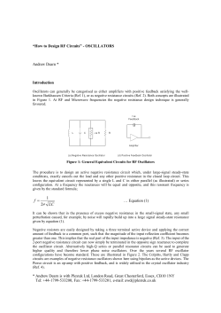


© Copyright 2026