
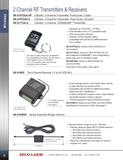
ENG - NTLab
CML Transmitter SPECIFICATION 1 FEATURES 2 TSMC CMOS 65 nm 1.2 V digital power supply 1.2 V CMOS input logic signals 8-step (3-bit) adjustable transmitter output current (range from 4 mA to 32 mA) 3.125 Gbps (DDR MODE) switching rates Temperature range: -40 °C to +125 °C Supported foundries: TSMC, UMC, Global Foundries, SMIC APPLICATION 3 Point-to-point data transmission Multidrop buses Clock distribution Backplane receiver Backplane data transmission Cable data transmission OVERVIEW Core logic interface includes signal pins (INp1, INp2 and INn1, INn2) for data transmission, control pin EN_TX to configure transmitter state and control pin EN_PR to toggle pre-emphasis mode. Data on signal pins INp2 and INn2 should be one bit shifted (delayed) from that on INp1 and INn1 for pre-emphasis purposes. IREF_TX is a reference current input. Differential CML output pins PAD_OUTp and PAD_OUTn should be connected to bonding pads. CML transmitter is designed on TSMC CMOS 65nm technology. 4 STRUCTURE Figure 1: CML transmitter structure. Ver. 1.1 May 2015 www.ntlab.com 065TSMC_CML_02 CML Transmitter 5 PIN DESCRIPTION Name IREF_i10uTX EN_TX EN_PR INp1 INn1 INp2 INn2 PAD_OUTp PAD_OUTn vdd12 gnd Direction I I I I I I I O O IO IO Table 1: CML transmitter truth table. Input Mode EN_TX Transmit 1 Power down 0 Ver. 1.1 Description Reference current 10 uA CML transmitter enable CML pre-emphasis enable Input complementary CMOS signals Input complementary CMOS signals, one bit shifted Output differential CML signal of transmitter Supply voltage 1.2 V Ground Output INp 0 1 X page 2 of 6 PAD_OUTp 0 1 Z PAD_OUTn 1 0 Z www.ntlab.com 065TSMC_CML_02 CML Transmitter 6 LAYOUT DESCRIPTION CML transmitter dimensions are given in the table 2. Table 2: Block dimensions. Dimension Height Width Value 176 196 Unit um um Figure 2: CML transmitter layout view. 1. Reference bias 2. Output stage 3. Digital buffers 4. Internal terminator 5. Filtering capacitor for bias voltage Ver. 1.1 page 3 of 6 www.ntlab.com 065TSMC_CML_02 CML Transmitter 7 OPERATING CHARACTERISTICS 7.1 TECHNICAL CHARACTERISTICS Technology __________________________________________________ TSMC CMOS 65 nm Status ____________________________________________________________ silicon proven Area__________________________________________________________________ 0.35 mm2 7.2 ELECTRICAL CHARACTERISTICS The values of electrical characteristics are specified for Vdd12= 1.14 ÷ 1.26 and T = -40 ÷ +125 °C, RL=50Ω (load resistance). Typical values are at Vdd12= 1.2V, T= +85 °C, unless otherwise specified. Value Parameter Symbol Condition Unit min typ max Supply digital voltage Vdd12 1.14 1.2 1.26 V Operating temperature range T -40 +85 +125 °C EN_PR = “0” 400 800 1600 mV Differential output voltage VOD EN_PR = “1” 400 800 1800 mV Output offset voltage VOS 0.8 1 1.1 V |Change VOD| ΔVOD 50 mV |Change VOS | ΔVOS Stand-by current Ist 2 µA Input voltage range Vin 0 1.2 V Output current Iout IREF_i10uTX=10µA 16 mA IREF_i10uTX=10 µA 1.9 2 2.1 mA DC power current from Vdd EN_PR = “0” random data without output IVDD IREF_i10uTX=10µA current 4.4 4.5 4.6 mA EN_PR = “1” IREF_i10uTX=10µA 2.18 2.4 2.62 mW EN_PR = “0” Total power without output Ptotal current IREF_i10uTX=10µA 5.06 5.4 5.75 mW EN_PR = “1” Differential time propagation tPHLDT delay, high to low 160 225 275 ps Differential time propagation tPLHDT delay, low to high Rise time tRT 100 ps CL=1p Fall time tFT 100 ps AC power current from Vdd IVDD 32.6 37.76 45.4 mA Total AC power W 37.5 45.31 56.72 mW Clock jitter, random rms tRJ 78 100 240 fs Clock jitter, random max (p-p) tDJM CL=1p 0.42 0.88 1.33 ps Data jitter, deterministic tDJ 0.42 0.88 1.33 ps Duty cycle S 48 49 50 % Input voltage high level VIH For digital inputs 0.8Vdd12 Vdd12 V Input voltage low level VIL For digital inputs 0 0.2 Vdd12 V Ver. 1.1 page 4 of 6 www.ntlab.com 065TSMC_CML_02 CML Transmitter 8 TYPICAL CHARACTERISTICS Figure 3: The time diagram of the transmitter at a frequency of 2 GHz. Figure 4: The time diagram of the transmitter at a frequency of 2 GHz with preemphasis. Ver. 1.1 page 5 of 6 www.ntlab.com 065TSMC_CML_02 CML Transmitter Figure 5: Transmitter ‘’eye’’ diagram. 9 DELIVERABLES IP contents: Ver. 1.1 Schematic or NetList Layout or blackbox Extracted view (optional) GDSII DRC, LVS, antenna report Test bench with saved configurations (optional) Documentation page 6 of 6 www.ntlab.com


© Copyright 2026