
Keywords:
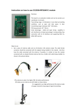
Maxim > Design Support > Technical Documents > Application Notes > Wireless and RF > APP 5417
Keywords: transmitter, receiver, ISM, RF, radio, PCB, antenna, impedance, range, matching, crystal, baseband, tuning, data rate, ASK, modulation
APPLICATION NOTE 5417
How to Optimize an ISM Radio Frequency (RF) System
By: Martin Stoehr, Principal Member of the Technical Staff, Applications
Oct 01, 2012
Abstract: With industrial/scientific/medical (ISM) band radio frequency (RF) products, often times users are new to the structure of Maxim's low pin-count transmitters and
fully integrated superheterodyne receivers. This tutorial provides simple steps that can be taken to get the best performance out of these transmitters and receivers while
providing techniques to measure the overall capability of the design.
A similar, Korean version of this article appears on EP&C News, September 6, 2012.
Introduction
Every day more industrial, scientific, and medical (ISM) band radio frequency (RF) products reach the marketplace. With so many
offerings available, it is not surprising that users are often unfamiliar with the structure of low-pin-count transmitters and fully integrated
superheterodyne receivers. This tutorial presents simple steps that designers can follow to achieve the best performance from these
transmitters and receivers. Techniques to measure the overall capability of these designs are also provided.
Click here for an overview of the wireless
components used in a typical radio
transceiver.
Transmitter Optimization
There are only two basic steps used to optimize the operation of a simple ISM transmitter (shown in Figure 1): make sure that the reference frequency is properly tuned,
and correctly match the output network of the transmitter to the antenna. A crystal oscillator is commonly used as the reference in both the transmitter and receiver circuits,
so that optimization technique is addressed in the Receiver Optimization section below.
Figure 1. Basic ISM transmitter circuit.
Matching the Transmitter (Tx) Antenna
For the initial matching of a Tx antenna, an S11 measurement (Figure 2A) is taken using a coax extension to the antenna feed point. The impedance transformation circuit
(Figure 1) was designed as a lowpass π network which accomplishes two things: first, it matches the power amplifier (PA) output impedance (modeled as 200Ω + j0) to the
complex conjugate of the antenna impedance (measured to be ~2.69Ω - j80.6 handheld, Figure 2, Figure 4); and second, it provides lowpass filtering to suppress
harmonics. In this instance, the value of the bias inductor for the PA is chosen to tune out the 2.0pF to 2.5pF stray capacitance to ground at the PA output. The series
capacitor, C8, serves as a DC block.
A
B
Figures 2A and B. Measured impedance (A, top) and calculated network (B, bottom).
Page 1 of 7
Using LLSmith, 1 a collection of components can be approximated very quickly. The Smith chart plot of the theoretical match is shown in Figure 2B. Because the antenna is
electrically small, it has a high Q (~30). Therefore, it is usually necessary to adjust the theoretical matching component values to compensate for variations in the antenna
impedance from its environment, parasitic reactance, and losses from the matching components and circuit board. The network values used for tuning were L1 = 62nH, C8
= 100pF, C9 = 15pF, L2 = 39nH, and C10 = open.
After establishing a starting point, adjustments are guided by measuring the transmitted power and the PA current as a function of frequency. The measurement setup is
shown in Figure 3. The fixed crystal is removed from the board; an external signal generator is connected through a blocking capacitor to the crystal pin to allow the
adjustment of frequencies from about 11MHz to 15MHz (for transmitted RF from 352MHz to 480MHz). The peak-to-peak voltage from the generator is set to about 500mV.
Figure 3. Adjustment circuit allows for frequency adjustment from ~11MHz to 15MHz.
At each frequency, the transmitted power and PA current are measured and the results are plotted. Component values in the matching network are changed (Figure 1) until
an optimized current minimum and a power maximum are achieved near the desired frequency (in this case 434MHz).
Figure 4. Optimizing the matching network obtains a current minimum and power maximum near the desired frequency.
Using this method, the match that gave the minimum PA current and maximum transmitted power consists of the following component values: L1 = 62nH; C8 = 100pF; C9
= 7.5pF; L2 = 51nH; and C10 = open.
The plot of current versus frequency (Figure 5) shows how each change in the matching network moved the current minimum to a different frequency. The graph for the
best match at 434MHz is shown in yellow. Notice that the values of C9 and L2 have changed noticeably (from 15pF and 39nH) as a result of the component and board
parasitic contributions.
A
B
Figure 5. Transmitter current plots show how changes in the matching network changed the current minimum.
The process of matching for Tx, PA power, operational frequency, and antenna impedances can be found in application notes 1954, "Designing Output Matching Networks
Page 2 of 7
for the MAX1472 ASK Transmitter," and 3401, "Matching Maxim's 300MHz to 450MHz Transmitters to Small Loop Antennas."
Receiver Optimization
The basic steps for optimizing the operational characteristics of an ISM superheterodyne receiver start with a systematic evaluation of the receiver blocks. There are
commonly four blocks where performance can be improved: the crystal oscillator circuit, the antenna matching circuit, the tank circuit, and the baseband circuit.
Selecting the Proper Crystal
One of the most common challenges associated with crystal-based receivers and transmitters is proper tuning of the radio's oscillation circuit. The oscillator on ISM radios
is intended to operate using a crystal specified with a specific load capacitance (Figure 6). In some ISM receivers, the crystal is typically specified for a 3pF load
capacitance. This low value is not a very common specification for crystals. Typically because of cost or supply considerations, customers attempt to design a system using
a crystal with a tested load capacitance of 6pF, 8pF, 10pF, or more. Using these larger load capacitance crystals is not prohibitive, but does present a trade-off since the
oscillator circuit will only provide the specified load capacitance to the crystal pins. For example, a 3pF load will cause a 10pF specified crystal to operate at a noticeably
higher frequency than intended. (For more information, see application note 1017, "How to Choose a Quartz Crystal Oscillator for the MAX1470 Superheterodyne
Receiver.") To compensate for this shift in frequency, a customer can present a larger load to the crystal by placing capacitors in the circuit. Our experience recommends
two shunt capacitors to ground rather than a parallel arrangement for enhanced flexibility and other loading benefits. The trade-off with this "adjusted" load is that too much
capacitance connected to the circuit could cause a problem with the oscillation startup.
Figure 6. Basic crystal circuit.
A debug measurement was made to investigate the oscillating frequency of the crystal populated on the above reference design. To perform this test, an R&S® ZVL3
spectrum analyzer and a "sniffer" antenna were used to probe the crystal frequency. This antenna was held in close proximity to the crystal (or touching one of the leads,
as needed) to obtain an estimate of the operating frequency. The system was populated with a 13.2256MHz crystal that had a specified C L of 8pF, but the oscillator circuit
only provided about 3pF of load. The peak of this system was measured at 13.23049MHz, which is high by 370ppm. This translates to an operating frequency of
434.085MHz (32 × 13.23049 + 10.7), which placed the expected LO and carrier frequency 165kHz higher than intended. This off-frequency operation of the crystal
oscillator resulted in an incoming ASK carrier and associated sidebands being pushed to the edge and even past the "knee" of the IF filter. This caused an unnecessary
attenuation of the signal power.
To further test the impact of this frequency error, the passband of the IF was tested. By sweeping the carrier signal in frequency and monitoring the IF filter output with the
spectrum analyzer in max-hold mode, a plot of the filter bandwidth was collected. Marker M1 was placed at 10.7MHz (nominal center of the IF filter) and the delta marker,
D2, was placed at the frequency spike where the RF signal was tuned to 433.92MHz. The signal generator was set to 434.085MHz when the IF spike was at M1,
confirming the shift in LO frequency. The plot illustrated in Figure 7 shows that the mistuning degrades the carrier by about 7dB. Sideband information needed for ASK
demodulation is actually attenuated further, and distorted due to the nonlinear location on the filter curve.
Figure 7. IF filter bandwidth, max-hold sweep.
The following entries were used for the estimates for a specified load capacitance of the crystal at 8pF: a MAX7034 ISM receiver; C PAR = 1.8pF; C SHUNT = 0pF; C SER =
10000pF (an AC short); f0 = 13.2256MHz; C 0 = 2.8pF; C L = 8.24pF; R1 = 60Ω; and C1 = 11.1fF. With these values, a pulling calculation showed an actual RF frequency of
434.0853MHz. (For more information, see application note 5422, "Crystal Calculations for ISM-RF Products.") Then by adding experimental shunt capacitance values, a
pair of 10pF capacitors will adjust the oscillation frequency back to the target value and, assuming that the other crystal values are well estimated, the startup margin will
be acceptable. The negative resistance calculation was -291.5Ω, compared to 4 × R1 of 240Ω. This left about -50Ω of additional margin.
As a first-order attempt to improve the sensitivity of the demonstration LFRD014: Tube Motor Receiver Reference Design module, two 10pF shunt caps were added at C21
and C22. The resulting crystal oscillator frequency was confirmed to have moved and was now operating at the corrected frequency of 13.226MHz. After adjusting the RF
Page 3 of 7
generator to be centered back at 433.92MHz, sensitivity was measured at -107dBm. This 12.4dB improvement resulted from the proper tuning of the reference frequency
for the local oscillator.
Matching the Antenna
The next step in tuning a receiver design is to measure the antenna impedance. A connection to the antenna feed point (if using a PCB trace antenna) is necessary. Prior
to attaching a coaxial cable, the network analyzer needs to be properly calibrated out to the end of a flexible coaxial as a port extension. The network analyzer should be
set to an appropriate frequency range of interest; the power output of Port 1 should be set to a reasonable level (-30dBm) so it does not overdrive the low-noise amplifier
(LNA). Finally, an S11 measurement can be made and the results will be displayed on a Smith chart.
There may be difficulty obtaining repeatable measurements based on the form factor of the antenna, the enclosure, and the test environment (human body influences,
further enclosure in an automobile, etc.). In this example the antenna was measured to be an impedance of 205Ω - j39 (Figure 8A).
A
B
Figure 8A and B. Measured impedance (A, top) and matching calculations (B, bottom) for the receiver antenna.
To properly choose the components for the matching network, it was also necessary to measure the impedance of the LNA. To do this, the network analyzer is used to
measure the S11 parameters of the design at the other side of the matching network looking into the LNA circuit. Commonly, the amplifier uses a degeneration inductor
connected between an LNA source pin and ground (Figure 9). When the degeneration inductor is present, the LNA input impedance looks like a 50Ω resistor in parallel
with a 2pF to 2.5pF capacitor. (Without the inductor, the input impedance looks like a 500Ω to 700Ω resistor in parallel with a 2pF to 2.5pF capacitor.) These impedance
models can be used to design matching networks for any antenna impedance.
Figure 9. Basic ISM receiver input.
In this example the measurement resulted in an impedance of 50 – j4Ω. Using the free Smith chart software package LLsmith 1 and entering the LNA bias network
component values of 100pF (C6) and 56nH (L3) with C4 shorted and C5 open, the LNA input impedance was back-calculated to be about 50 + j145Ω.
To find the final matching network components, the software can provide the best estimate of values for populating the receiver board (Figure 8B). Consequently, using the
"Simple MatchMe Wizard" and entering the starting impedance of 205 + j39 (the complex conjugate of the antenna impedance), the ending impedance of 50 – j145 (the
complex conjugate of the LNA impedance), and using the lumped lowpass, 1 section setting, LLsmith estimated the matching network components to be (from LNA to
antenna):
9.4pF series capacitor
3.2pF shunt capacitor
32.3nH series inductor
2.1pF series capacitor
Tuning the Tank Circuit
The next step for optimizing the receiver design is to ensure that the tank circuit at the LNA output and mixer input is well tuned to the operating frequency (Figure 10).
This off-chip inductor-capacitor pair provides a tuned, high-impedance circuit that converts the LNA current output into a voltage which, in turn, is fed to the on-chip mixer.
This circuit can be easily mistuned by stray capacitances found on the circuit board.
Page 4 of 7
Figure 10. Receiver tank circuit.
The best method to determine whether the tank circuit is properly tuned is to sweep the input frequency and look for the peak on the measured resonance curve. Data can
be collected manually with an RF generator and a spectrum analyzer, but a two-port network analyzer (NA) is the best tool for the job. The stimulus comes from the
network analyzer (Port 1) connected to the LNA through the antenna feed. The measurement is taken by using a sniffer antenna connected to the input (Port 2) of the
network analyzer. This untuned antenna can be held in close proximity to the inductor of the tank circuit (Figure 11) and it will pick up radiated emissions at the circuit's
resonant frequency and provide an S21 measurement. The use of a -20dBm or -30dBm source power setting is recommended to avoid putting the LNA input into
overdrive.
Figure 11. Sniffing the tank circuit.
The suggested component values for the example tank circuit were a 27nH inductor in parallel with no capacitor. This approach simply allows the parasitics of the PCB to
act as the resonant capacitive element. The resonant frequency of a tank circuit can be calculated from the following equation:
ω 0 ² = (2πf 0 )² = 1/LC or f0 = 1/(2π√LC)
The initial measurements of this example (Figure 12) showed a peak resonance around 480MHz. At the target frequency of 434MHz the system showed a loss of 10dB
from that peak.
Figure 12. Tank circuit frequency before tuning.
Given that L5 = 27nH, the actual parasitic capacitance can be extracted using the same equation to calculate a suggested value for C7. With the example circuit operating
at 480MHz, the parasitic capacitance, C P , would be about 4.07pF:
C P = 1/((27nH)(2π480MHz)²)
Given the target resonant frequency of 434MHz, the ideal capacitance becomes 4.98pF. Thus, the added capacitance need for the tank circuit is about 0.91pF:
C7 = 1/((27nH)(2π434MHz)²) – 4.07pF
Adding a 1.0pF capacitor to the C7 location improved the sensitivity of this example. With the adjusted tank circuit, the S21 measurement indicated the peak to be very
near the target of 434MHz (Figure 13).
Page 5 of 7
Figure 13. Tuned tank circuit.
Measuring Receiver Gain
The system's gain from the LNA input to the mixer output serves as an interim check on the receiver's performance. This parameter was measured on the example
receiver by providing an input carrier signal at 433.92MHz with an amplitude of -50dBm. The output was then measured from the MIXOUT line (at the ceramic filter) using a
high-impedance FET probe connected to the spectrum analyzer. In this case the input power can either be noted from the generator setting or be measured at the antenna
feed. When measuring the input and output signals at the filter, it is recommended that any digital noise coming from the baseband circuit be eliminated. This is easily
accomplished by grounding the DSN line (effectively dropping the slicer level below the noise) while collecting the spectrum analyzer plots.
For this example, the input signal was measured to be -49.9dBm at the antenna feed point. The signal strength at the filter input was measured to be -35.5dBm with a 10x
probe (accounting for a 20dB drop in the measured power), which translates to an actual output of -15.5dBm. These numbers reveal that the system gain from the LNA to
the mixer output is about 34.4dB.
Optimizing the Baseband
The target data rate of the baseband circuit (Figure 14) should be designed with the corner frequency at 1.5 times the fastest expected data rate from the transmitter.
Since this example system was targeting 1kbps NRZ, the corner frequency of the data filter would be 1.5kHz. 5 (Manchester encoding is recommended. See application
note 3435, "Manchester Data Encoding for Radio Communications" for more information.)
To determine a Sallen-Key Butterworth data filter, use:
C13 (CDFFB) = 1/(141.4kπf C) = 1/(141.4kπ1.5k) = 1500.7pF
C12 (COPP) = 1.414/(400kπf C) = 1.414/(400kπ7.2k) = 750.1pF
Figure 14. Receiver baseband circuit.
Given the preceding calculations, a 1500pF capacitor value was selected for C13 and a 750pF capacitor value was selected for C12 in the example circuit. The time
constant of the RC circuit provides an averaging process that further filters the data output to form the threshold voltage of the data slicer comparator. This time constant
should be set to approximately 10x the bit interval of the data rate (1kHz). The starting point R1 = 20kΩ, C17 = 0.47µF was chosen, which is only about a 1-bit interval.
More information regarding the receiver baseband and data slicing circuitry can be found in application note 3671, "Data Slicing Techniques for UHF ASK Receivers" and
tutorial 5426, "Baseband Calculations for ISM-RF Receivers."
References
RFdude.com Smith Chart Program, RFdude.com LLC, Lance Lascari, © 2008–2010, v0.810, Jun 2007,
http://tools.rfdude.com/RFdude_Smith_Chart_Program/RFdude_smith_chart_program.html.
R&S is a registered trademark and registered service mark of Rohde & Schwarz GmbH & Co. KG.
Related Parts
MAX1470
315MHz Low-Power, +3V Superheterodyne Receiver
Free Samples MAX1471
315MHz/434MHz Low-Power, 3V/5V ASK/FSK Superheterodyne Receiver
Free Samples Page 6 of 7
MAX1472
300MHz-to-450MHz Low-Power, Crystal-Based ASK Transmitter
Free Samples MAX1473
315MHz/433MHz ASK Superheterodyne Receiver with Extended Dynamic Range
Free Samples MAX1479
300MHz to 450MHz Low-Power, Crystal-Based +10dBm ASK/FSK Transmitter
Free Samples MAX7030
Low-Cost, 315MHz and 433.92MHz ASK Transceiver with Fractional-N PLL
Free Samples MAX7031
Low-Cost, 308MHz, 315MHz, and 433.92MHz FSK Transceiver with Fractional-N PLL
Free Samples MAX7032
Low-Cost, Crystal-Based, Programmable, ASK/FSK Transceiver with Fractional-N PLL
Free Samples MAX7033
315MHz/433MHz ASK Superheterodyne Receiver with AGC Lock
Free Samples MAX7034
315MHz/434MHz ASK Superheterodyne Receiver
Free Samples MAX7036
300MHz to 450MHz ASK Receiver with Internal IF Filter
Free Samples MAX7042
308MHz/315MHz/418MHz/433.92MHz Low-Power, FSK Superheterodyne Receiver
Free Samples MAX7044
300MHz to 450MHz High-Efficiency, Crystal-Based +13dBm ASK Transmitter
Free Samples MAX7049
High-Performance, 288MHz to 945MHz ASK/FSK ISM Transmitter
Free Samples MAX7057
300MHz to 450MHz Frequency-Programmable ASK/FSK Transmitter
Free Samples MAX7058
315MHz/390MHz Dual-Frequency ASK Transmitter
Free Samples MAX7060
280MHz to 450MHz Programmable ASK/FSK Transmitter
Free Samples More Information
For Technical Support: http://www.maximintegrated.com/support
For Samples: http://www.maximintegrated.com/samples
Other Questions and Comments: http://www.maximintegrated.com/contact
Application Note 5417: http://www.maximintegrated.com/an5417
APPLICATION NOTE 5417, AN5417, AN 5417, APP5417, Appnote5417, Appnote 5417
Copyright © by Maxim Integrated
Additional Legal Notices: http://www.maximintegrated.com/legal
Page 7 of 7


© Copyright 2026