ABC
docz
Explore
Log in
Create new account
Download
Report
technology and computing
hardware
MC9S08PA4 Reference Manual Supports: MC9S08PA4(A) Document Number: MC9S08PA4RM Rev 3, 08/2014
How to Reboot/Shutdown Splicecom Maximiser 4140 Callserver
Second Grade Sight Word List Name:____________
THE HOOK (AND PATTERN INTERRUPT)
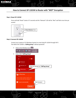
Edimax SP-1101W WEP Setup Guide
Business Plan
How To Change the IP address On
How to upgrade your DualRunners ?
Document 213577
How to change between DM9161, DM9161A and DM9161B 1.
Dell AXIM X30/X50/X50v wireless setup
© Copyright 2026
About abcdocz
DMCA / GDPR
Report