
Programming and Software Manual Medium Voltage Variable Speed Drive Series MEDIUM VOLTAGE
Series MEDIUM VOLTAGE VARIABLE SPEED DRIVE Medium Voltage Variable Speed Drive Programming and Software Manual Variable Speed Drive Programming and Software Manual XMV660_A0.0.10 Edition: April 2014 XMV66MTSW01DI Rev. D XMV660 VSD 2 POWER ELECTRONICS XMV660 VSD POWER ELECTRONICS SAFETY SYMBOLS Always follow safety instructions to prevent accidents and potential hazards from occurring. WARNING This symbol means improper operation may results in serious personal injury or death. CAUTION Identifies shock hazards under certain conditions. Particular attention should be given because dangerous voltage may be present. Maintenance operation should be done by qualified personnel Identifies potential hazards under certain conditions. Read the message and follow the instructions carefully. Identifies shock hazards under certain conditions. Particular attention should be given because dangerous voltage may be present. Edition of April 2014 This publication could present technical imprecision or misprints. The information here included will be periodically modified and updated, and all those modifications will be incorporated in later editions. To consult the most updated information of this product you might access through our website www.power-electronics.com where the latest version of this manual can be downloaded. 3 XMV660 VSD POWER ELECTRONICS Revisions 4 Date Revision Description 28 / 02 / 2013 19 / 07 / 2013 18 / 10 / 2013 30 / 04 / 2014 A B C D First edition. SW version A0.0.5 SW version A0.0.6 SW version A0.0.7 SW version A0.0.10 POWER ELECTRONICS XMV660 VSD INDEX SAFETY INSTRUCTIONS ........................................................................................................... 7 1. DISPLAY UNITAND CONTROL KEYPAD........................................................................... 1.1. LEDs for Status Indication .......................................................................................... 1.2. Alphanumeric LCD Display ........................................................................................ 1.3. Control Keys .............................................................................................................. 11 11 11 12 2. STATUS MESSAGES .......................................................................................................... 2.1. List of Status Messages ............................................................................................. 2.2. List of Warning Messages .......................................................................................... 14 14 16 3. VISUALIZATION MENU ....................................................................................................... 3.1. Parameters SV.1 – Motor Visualization...................................................................... 3.2. Parameters SV.2 – Drive Visualization ...................................................................... 3.3. Parameters SV.3 – External Visualization.................................................................. 3.4. Parameters SV.4 – Internal Visualization ................................................................... 3.5. Parameters SV.5 – Programmable Parameters ......................................................... 3.6. Parameters SV.6 – Registers ..................................................................................... 3.7. Parameters SV.9 – Cell Status .................................................................................. 17 18 18 19 20 20 20 21 4. DESCRIPTION OF PROGRAMMING PARAMETERS ........................................................ 4.1. Group 1 – G1: Options Menu ..................................................................................... 4.2. Group 2 – G2: Name plate motor ............................................................................... 4.3. Group 3 – G3: References ......................................................................................... 4.4. Group 4 – G4: Inputs.................................................................................................. 4.5. Group 5 – G5: Acceleration and Deceleration Rates ................................................. 4.6. Group 6 – G6: PID Control ......................................................................................... 4.7. Group 7 – G7: Start / Stop Control ............................................................................. 4.8. Group 8 – G8: Outputs ............................................................................................... 4.9. Group 9 – G9: Comparators....................................................................................... 4.10. Group 10 – G10: Limits .............................................................................................. 4.11. Group 11 – G11: Protections ..................................................................................... 4.12. Group 12 – G12: Auto Reset...................................................................................... 4.13. Group 13 – G13: Fault History ................................................................................... 4.14. Group 14 – G14: Multi-references .............................................................................. 4.15. Group 15 – G15: Inch Speeds ................................................................................... 4.16. Group 16 – G16: Skip Frequencies ............................................................................ 4.17. Group 17 – G17: Brake .............................................................................................. 4.18. Group18 _ G18 : Encoder ......................................................................................... 4.19. Group 19 – G19: Fine Tune ....................................................................................... 4.20. Group 20 – G20: Serial Comms ................................................................................. 4.21. Group 21 – G21: Networks ........................................................................................ 4.22. Group 23 – G23: Cells ............................................................................................... 22 23 24 25 26 36 37 38 40 45 49 50 52 54 55 55 55 56 56 57 58 61 63 5. MODBUS COMMUNICATION .............................................................................................. 5.1. Supported Modbus Function Codes ........................................................................... 5.2. Addressing Modes ..................................................................................................... 5.3. Remote Control Functions ......................................................................................... 5.4. Summary of Modbus Addresses ................................................................................ 65 65 66 67 68 6. WI-FI CONNECTION ............................................................................................................ 84 7. FAULT MESSAGES. DESCRIPTION AND ACTIONS ........................................................ 7.1. Description of Fault List.............................................................................................. 7.2. Procedure for Fault Solutions ..................................................................................... 88 89 90 8. CONFIGURATION REGISTER ............................................................................................ 93 INDEX 5 XMV660 VSD 6 INDEX POWER ELECTRONICS XMV660 VSD POWER ELECTRONICS SAFETY INSTRUCTIONS IMPORTANT! Read this manual carefully to maximise the performance of this product and to ensure its safe use. In this manual, safety messages are classified as follows: WARNING Do not remove the cover while the power is applied or the unit is in operation. Otherwise electric shock could occur. Do not run the drive with the front cover removed. Otherwise you may get an electric shock due to the high voltage terminals or exposure of charged capacitors. Do not remove the cover except for periodic inspections or wiring, even if the input power is not applied. Otherwise you may access the charged circuits and get an electric shock. Wiring and periodic inspections should be performed at least 20 minutes after disconnecting the input power and after checking the red LED “Bus voltage” of the cells is turn off. Otherwise you may get an electric shock. Operate the switches with dry hands. Otherwise you may get an electric shock. Do not use cables with damaged insulation. Otherwise you may get an electric shock. Do not subject the cables to abrasions, excessive stress, heavy loads or pinching. Otherwise, you may get an electric shock. SAFETY INSTRUCTIONS 7 XMV660 VSD POWER ELECTRONICS CAUTION Install the drive on a non-flammable surface. Do not place flammable material nearby. Otherwise fire could occur. Disconnect the input power if the drive gets damaged. Otherwise it could result in a secondary accident or fire. After the input power is applied or removed, the drive will remain hot for a couple of minutes. Touching hot parts may result in skin burns. Do not apply power to a damaged drive or to a drive with parts missing even if the installation is complete. Otherwise you may get an electric shock. Do not allow lint, paper, wood chips, dust, metallic chips or other foreign matter into the drive. Otherwise fire or accident could occur. WARNINGS RECEPTION The XMV660 is carefully tested and perfectly packed before leaving the factory. In the event of transport damage, please ensure that you notify the transport agency and POWER ELECTRONICS: 902 40 20 70 (International +34 96 136 65 57) or your nearest agent, within 24hrs from receipt of the goods. UNPACKING Make sure model and serial number of the variable speed drive are the same on the box, delivery note and unit. Each variable speed drive is supplied with a XMV660 technical manual. RECYCLING Packing of the equipments should be recycled. For this, it is necessary to separate different materials included (plastic, paper, cardboard, wood, ...) and deposit them on proper banks. Waste products of electric and electronic devices should be selectively collected for their correct environmental management. EMC This type of PDS (Power Device System) is not intended to be used on a low-voltage public network which supplies domestic premises. Radio frequency interference is expected if used on such a network. 8 SAFETY INSTRUCTIONS POWER ELECTRONICS XMV660 VSD SAFETY Before operating the drive, read this manual thoroughly to gain and understanding of the unit. If any doubt exists then please contact POWER ELECTRONICS, (902 40 20 70 / +34 96 136 65 57) or your nearest agent. Wear safety glasses when operating the drive with power applied and the front cover is removed. Handle the drive with care according to its weight. Install the drive according to the instructions within this manual. Do not place heavy objects on the drive. Ensure that the mounting orientation is correct. Do not drop the drive or subject it to impact. The XMV660 drives contain static sensitive printed circuits boards. Use static safety procedures when handling these boards. Avoid installing the drive in conditions that differ from those described in the Technical Characteristics section. CONNECTION PRECAUTIONS To ensure correct operation of the drive it is recommended to use a SCREENED CABLE for the control wiring. For EMERGENCY STOP, make sure supply circuitry is open. Do not disconnect motor cables if input power supply remains connected. The internal circuits of the XMV660 Series will be damaged if the incoming power is connected and applied to output terminals (U, V, W). It is not recommended to use a 3-wire cable for long distances. Due to increased leakage capacitance between conductors, over-current protective feature may not operate correctly. Do not use power factor correction capacitors, surge suppressors, or RFI filters on the output side of the drive. Doing so may damage these components. Always check whether the DC BUS (in each cell) red LED is OFF before wiring terminals. The capacitors may hold high-voltage even after the input power is disconnected. Use caution to prevent the possibility of personal injury. TRIAL RUN Verify all parameters before operating the drive. Alteration of parameters may be required depending on application and load. Always apply voltage and current signals to each terminal that are within levels indicated within this manual. Otherwise, damage to the drive may result. SAFETY INSTRUCTIONS 9 XMV660 VSD POWER ELECTRONICS OPERATION PRECAUTIONS When the Auto Restart function is enabled, keep clear of driven equipment, as the motor will restart suddenly after a fault is reset. The “STOP / RESET” key on the keypad is active only if the appropriate function setting has been made. For this reason, install a separate EMERGENCY STOP push button that can be operated at the equipment. If a fault reset is made with the reference signal still present then a restart will occur. Verify that it is permissible for this to happen, otherwise an accident may occur. Do not modify or alter anything within the drive. Before programming or operating the XMV660 Series, initialise all parameters back to factory default values. EARTH CONNECTION 10 The drive is a high frequency switching device and leakage current may flow. Ground the drive to avoid electrical shock. Use caution to prevent the possibility of personal injury. Connect only to the dedicated ground terminal of the drive. Do not use the case or the chassis screw for grounding. When installing, grounding wire should be connected first and removed last. The earth cable must have a minimal cross sectional area that meets local country electrical regulations. Motor ground must be connected to the drive ground terminal and not to the installation’s ground. We recommend that the section of the ground connection cable should be equal or higher than the active conductor. Installation ground must be connected to the drive ground terminal. SAFETY INSTRUCTIONS XMV660 VSD POWER ELECTRONICS 1. DISPLAY UNIT AND CONTROL KEYPAD The display of the XMV660 is removable for remote installation, as the illustration shows. There are three leds on the display which indicate the drive operational status, one LCD screen with 4 lines of 16 characters each and keys for control and parameter setting. Figure 1.1 Display Unit and Keypad 1.1. LEDs for Status Indication Leds offer an easy method of identifying if the XMV660 is powered up, if the drive is supplying output voltage, or if the drive has tripped. Led ON: Yellow colour. When it is lit, indicates equipment is powered up. When it is blinking, indicates the drive gets any warning. Led RUN: Green colour. When it is lit, indicates the motor is powered by the XMV660. Led FAULT: Red colour. When it is blinking, indicates the equipment is in fault status. Figure 1.2 Status visualization DISPLAY UNIT AND CONTROL KEYPAD 11 XMV660 VSD POWER ELECTRONICS 1.2. Alphanumeric LCD Display XMV660 display has a LCD screen of four lines with sixteen characters each (16x4). Each line has different functions. Status Line: It is the top line. It is always present and shows the XMV660 status (STR – Start, STP – Stop, etc…). It also shows the output current and the motor speed. It is not configurable by the user. Visualization Line 1: It is the second line of the screen. It is always present and allows the selection of variables from the visualization menu. It is configurable by the user. Visualization Line 2: It is the third line of the screen. It is always present and allows the selection of variables from the visualization menu. It is configurable by the user. Programming Line: It is the fourth line. It is used to display and / or set different parameters within the XMV660. Figure 1.3 Detail of the Display Lines 1.3. Control Keys Function keys have multiple uses and can be operated individually or in combination with other keys: It allows access to different parameters groups and sub-groups; it displays code explanations and allows adjustment of parameter values in combination with other keys. If a group has no sub-groups, it allows direct access to the parameters of the group. To modify numeric parameters: & Simultaneously pushed, the value will increase. & Simultaneously pushed, the value will decrease. To modify parameters of numbered options: Pushing this key, the extended explanation will appear. & & Simultaneously pushed will ascend the user through the varying options. Simultaneously pushed will descend the user through the varying options. It allows upward movement through the parameters groups and allows navigation for different parameters within a parameter group. It also allows the increase of parameters value. It allows downward movement through the parameters groups and allows navigation for different parameters within a parameter group. It also allows the decrease of parameters value. 12 DISPLAY UNIT AND CONTROL KEYPAD XMV660 VSD POWER ELECTRONICS When pushed for 2 seconds (approx.) it allows navigation between the programming line and visualization lines available to the user. It also offers the possibility of escaping back to the previous sub-group or group. To start the drive from the keypad when the control has been set as local control (check drive configuration). To stop the drive from the keypad when the control has been set as local control. In the case of tripping this key can be used to reset the drive, if local control is enabled. In the following figure you can see a programming example where you can observe the operation explained previously. Figure 1.4 Example of parameters navigation DISPLAY UNIT AND CONTROL KEYPAD 13 XMV660 VSD POWER ELECTRONICS 2. STATUS MESSAGES The upper line of the display corresponds to the status line. In this line we can display the equipment status, motor current (A) and the motor speed (%). It is always displayed and it is not programmable by the user. Figure 2.1 Status Line Description Note: The user can access to the information displayed in status line via Modbus and Wi-Fi communication. See sections ‘Modbus Communication’ and ‘Wi-Fi Connection’. 2.1. List of Status Messages The following table includes the different status of the drive. Screen Name Description OFF ON ACL RUN DEC Deactivated power Activated power Accelerating Running Decelerating Free run stop when a fault occurs Drive power is deactivated. Drive power is activated. Drive is increasing the output frequency. Motor increasing in speed, it is accelerating. Drive is operating at reference speed. Operation at steady status. Drive is decreasing the output frequency. Motor decreasing in speed, it is decelerating. Drive is stopping by free run stop after a fault occurs (emergency stop). Motor stopping time is determined by inertia as the drive output has turned off. Drive is decreasing the output frequency due to a stop command. Motor is stopping by ramp until zero speed is reached. ‘Flying start’ operation must be configured if required. The XMV660 will search for the actual motor shaft speed once the drive has received a start command. The drive is getting the motor’s magnitudes values. When a delay time has been set in order to start the equipment, after the start command has been activated, this message will be displayed until this time has elapsed. EST 14 STP Stopping SPN Flying start AUT Autotunning DLY Start Delay Time GRAPHIC DISPLAY UNIT USAGE XMV660 VSD POWER ELECTRONICS Screen Name IN1 Inch speed 1 IN2 Inch speed 2 IN3 Inch speed 3 HEA Non condensing current is activated Description XMV660 is working according to inch speed 1 command and ‘Start + Inch speed 1' mode is active. When operated in this mode the "Start + Inch speed 1" command is dominant over other inputs programmed for "Start" functionality. Therefore if one input is configured as ‘Start’ and it is deactivated; in spite of this deactivated input, the drive will start when ‘Start + Inch speed 1' command is received. This is also valid for Inch speed 2 and 3. XMV660 is working according to inch speed 2 command. ‘Start + Inch speed 2' mode is active. XMV660 is working according to inch speed 3 command. ‘Start + Inch speed 3' mode is active. XMV660 is injecting DC current to prevent moisture condensing within the motor. CAUTION: Although the motor is not running there is dangerous voltage. Run Led will be lit during this process. Be careful to avoid damages and personal injury. The following table includes the different status of the cells. Screen OK V CTR LST BUS LOST TIME OUT OVER VOL GD FAULT UNDR VOL HIGH TEMP SOFT CHRG RMT UPGRD FB CNTR RMT UG OK Name Ok Control voltage loss Bus voltage loss Time out Over voltage GateDrive Fault Under voltage High temperature Fault of the Soft Charge Remote Upgrading in Progress Contactor feedback Fault Remote Upgrade Finished Description The cell operates properly The cell has lost the voltage control The cell has lost the bus voltage Time since the last transmission is longer than usual The cell voltage is higher than the nominal voltage A Gatedrive problem occurs in the cell The cell voltage is lower than the nominal voltage The cell temperature has reached a dangerous level The soft charge hasn’t been done correctly The remote upgrade is in progress The contactor feedback has not been received The remote upgrade has been finished correctly The following table includes the different status of the system. Screen Name COM OK READY START WAITING STOP Communication OK Ready Start Waiting Stop ERR COM Erroneous communication Description All communications are OK The communication between the modulator and the control board is correct. The system is started. The modulator is waiting for receiving frames from the control The system is stopped. There is a communication problem due to: - CRC received by the modulator is not correct - The status ‘WAITING’ takes longer than expected and changes to ‘COM ERR’ GRAPHIC DISPLAY UNIT USAGE 15 XMV660 VSD POWER ELECTRONICS 2.2. List of Warning Messages The following table includes the different warnings of the drive. Screen 16 Name MOL Motor overload MOC Motor over-current DOC Drive over-current ILT TLT Current limitation Torque limitation VLT Voltage limitation ACO AVO AVI Asymmetric current Output voltage imbalance Input voltage imbalance OVV High input voltage UNV Low input voltage CWR Cell Warning MVR Motor Voltage Remainder S1L S2L Speed limit 1 reached Speed limit 2 reached GRAPHIC DISPLAY UNIT USAGE Description This message will appear when motor thermal model is increasing the estimated motor temperature. Motor current is higher than the rated current value. This message will appear if the output current is higher than 125% of the nominal current. Current limit algorithm has been activated. Torque limit algorithm has been activated. A high DC Link voltage level has been detected and the voltage limit control algorithm has been activated to protect the drive. Asymmetry in output currents of the drive has been detected. Asymmetry in output voltage of the drive has been detected. Asymmetry in input voltage of the drive has been detected. Input voltage of the equipment is reaching a dangerous level. The value is above the set value (protections settings). Input voltage of the equipment is reaching a dangerous level. The value is below the set value (protections settings). One of the cells is in bypass. The user can access to the cell section and see which cell is in bypass. After making stop in the drive, the motor has an extra voltage higher than 10% of the rated motor voltage. Motor speed has reached speed limit 1. Motor speed has reached speed limit 2. XMV660 VSD POWER ELECTRONICS 3. VISUALIZATION MENU These parameters constantly indicate the input signal status and dynamic parameter status of the XMV660. Visualization lines are the second and the third lines. The user can select the parameter to be displayed in each line from the different visualization options. To select a display parameter you should move to the cursor to the second or third line. For this, you need to press ESC / key for approx two seconds. The cursor moves from one line to the next. Once located on the second or third line you can navigate like the programming line (line 4) and select the desired parameter to be displayed. Once selected these parameters are saved into memory. These parameters are then displayed on lines 2 and 3 whenever the drive is powered up. Thanks to these lines user can display desired parameters and obtain additional information easily. Visualization Lines These lines show specific parameters that can be useful for the user. XMV66ITC0039AI Figure 3.1 Visualization Lines Description VISUALIZATION MENU 17 XMV660 VSD POWER ELECTRONICS 3.1. Parameters SV.1 – Motor Visualization Screen Sp Ref = +000% Tq Ref = 0.0% Mtr speed = 0 rpm Mtr sp = 0.0% Mtr Freq = 0.0Hz Motr Vout = 0V Motr Iout= 0.0A Mtr Torqe = 0.0% Mtr Pfactr = 0.00 Mtr Pwr = +0.0kW 0.0 0.0 0.0A Vmt U-V = 0.0 V Vmt V-W = 0.0 V Vmt W-U = 0.0 V Units % motor speed % motor torque rpm % motor speed Hz V A % motor torque kW A V PTC Motor = 0 Motor Temp = 0.0% % Motor heat Enco.Pulso = 7 CLsped = 0 rpm rpm Description It shows the present reference value of speed which is applied to the motor. It shows the present reference value of the torque which is applied to the motor It shows the motor speed in revs per minute. It shows the motor speed in % It shows the frequency being applied to the motor. It shows the present voltage applied to the motor. It shows the present current flowing to the motor. It shows the present torque applied to the motor. It shows the power factor of the motor. It shows the instantaneous power consumption of the motor. It shows the instantaneous current of each phase of the motor (U, V and W). It shows the instantaneous voltage applied to the motor terminals. It shows if the motor PTC (temperature sensor) is connected. X: PTC Connected. 0: PTC Not Connected. It shows the estimated motor temperature. A level of 110% will cause F25 trip (motor overload). It shows the Encoder pulse It shows the speed seen by the Encoder. 3.2. Parameters SV.2 – Drive Visualization Screen L1-L2 Vin = 0V L2-L3 Vin = 0V L3-L1 Vin = 0V Inp Vol = 0V 50.0 50.0 50.0 Hz IGBT Temp = +23ºC Drive T. = +26ºC 0.0 0.0 0.0A Pow In = 1500 kW Phi Cos In = 0.82 18 VISUALIZATION MENU Units V V Hz ºC ºC A kW - Description It shows the input instantaneous voltage applied to the drive (RS, ST, RT). It shows the average input voltage to the drive. It shows the frequency of the input voltage to the drive. It shows the temperature measured at the power stage of the drive output. It shows the temperature measured inside the electronics chamber of the drive. It shows the input instantaneous current applied to the drive (R, S, T) It shows the instantaneous power applied to the drive It shows the input power factor of the drive XMV660 VSD POWER ELECTRONICS 3.3. Parameters SV.3 – External Visualization Screen ANLG IN1 = +0.0V AIN1 Refr = +0.00% AIN1 S = +0.00l/s ANLG IN2 = +0.0V AIN2 Refr = +0.00% AIN 2 S = +0.00Bar ANLG IN3 = +0.0V AIN3 Refr = +0.00% AIN3 S = +0.00l/s ANL OUT1 = +4.0mA AO1 Refer = +0.0% ANL OUT2 = +4.0mA AO2 Refer = +0.0% ANL OUT3 = +4.0mA AO3 Refer = +0.0% Units V or mA % bottom scale AI1 Engineering units V or mA % bottom scale AI2 Engineering units V or mA % bottom scale AI1 Engineering units V or mA % associated magnitude V or mA % associated magnitude V or mA % associated magnitude DI= 0000000000 0 - Relays 1-8: X000XXXX - M SPD= +0.000m/s Description It shows the value of Analogue Input 1. It shows the value or the PID reference proportional to Analogue Input 1 in percentage. It shows the value of sensor 1 associated to the Analogue Input 1. It shows the value of the Analogue Input 2. It shows the value or the PID reference proportional to the Analogue Input 2 signal. It shows the value of sensor 2 associated to the Analogue Input 2. It shows the value of Analogue Input 3. It shows the value or the PID reference proportional to Analogue Input 3 in percentage. It shows the value of sensor 3 associated to the Analogue Input 3. It shows the value of Analogue Output 1. It shows the magnitude value associated to the Analogue Output 1 (speed, current ...). It shows the value of Analogue Output 2. It shows the magnitude value associated to the Analogue Output 2 (speed, current ...). It shows the value of Analogue Output 3. It shows the magnitude value associated to the Analogue Output 3 (speed, current ...). It shows whether the Digital Inputs are activated or not, from DI1 to DI10. The final is another input which shows the status of the motor PTC signal. X: Active. 0: Not Active. It shows whether the output relays are activated or not. X: Active. 0: Not Active. It shows the speed of the motor in engineering units. Pressing key you can access to the following sub-parameters of configuration: Screen Range Description 0.001 To set the ratio factor between motor speed and Scale ftr=1 10 machine speed. It allows selection of the units to be displayed Depending on config. Units Ma=m/s Modbus Traffic:0 0/X m/s m/m cm/s cm/m v/s v/m Units Description m/s m/m cm/s cm/m v/s v/m Meters / second Meters / minute Centimetres / second Centimetres / minute Turns / second Turns / minute Note: They both are settable during run. “X” will be displayed if Modbus communication exists through RS232 or RS485 user port. Furthermore, “X” will blink at constant frequency while communication is active. After half second is elapsed without communication, “O” will be displayed. VISUALIZATION MENU 19 XMV660 VSD POWER ELECTRONICS 3.4. Parameters SV.4 – Internal Visualization Screen Actual Fault = 00 Drive Curr = 170A Drive Volt = 2300V S/W = mcXMV_A0.0.10 H/W = 1.00 PID R% = +0.0% PID F% = +0.0% Units Description A V % feedback range % AI used as feedback Comparators = 000 - FLT.STAT. = NO FLT NO FLT --- It shows the reference value in PID mode of the equipment standard program. It shows the feedback value in PID mode of the equipment standard program. It shows if comparators are activated or not. X: Active / 0: Not Active. It shows if the equipment is in faulty status. If the equipment is in faulty status, it shows the status of the drive before the fault is produced; when there is not fault, it shows ‘NO FLT’. When it is set to ‘Y’ (YES), the parameters of groups ‘SV.1 Motor Visualization’ and ‘SV.2 Drive Visualization’ are hold with the last values at the moment of the last fault is produced. If the user sets the parameter to ‘N’ (NO), or after 135 seconds are elapsed, the parameters will show the actual values again. The hold values are saved in memory until next fault will be produced, even if the input power of the drive is lost. N Y Fault Diag. = N It shows the present code fault. See fault history G13. It shows the drive rated current (maximum current of the equipment at 50ºC). It shows the drive rated voltage. It shows the software version installed into the equipment. It shows the hardware version of the equipment. 3.5. Parameters SV.5 – Programmable Parameters This group is not only a display group. Some parameters such as speed, pressure and inch speeds can be adjusted in this group. These parameters are also available in their corresponding parameter groups. This is a simple way to allow user adjustment of basic parameters without entering the main programming groups. Screen Units Description Local Sp = +100% % motor speed PID Local = +100% % feedback Mref 1 = +10.0% % motor speed Mref 2 = +20.0% % motor speed Mref 3 = +30.0% % motor speed Mref 4 = +40.0% % motor speed Mref 5 = +50.0% % motor speed Mref 6 = +60.0% % motor speed Mref 7 = +70.0% % motor speed Inch spd1 = 0.00% Inch spd2 = 0.00% Inch spd3 = 0.00% % motor speed % motor speed % motor speed It shows the speed reference value in local mode (introduced by keypad). See G3.3 parameter for additional data. It allows user to select the PID reference in local mode. See G6.2 parameter for additional data. It allows user to set the speed value assigned to Multi-reference 1. See G14.1 parameter for additional data. It allows user to set the speed value assigned to Multi-reference 2. See G14.2 parameter for additional data. It allows user to set the speed value assigned to Multi-reference 3. See G14.3 parameter for additional data. It allows user to set the speed value assigned to Multi-reference 4. See G14.4 parameter for additional data. It allows user to set the speed value assigned to Multi-reference 5. See G14.5 parameter for additional data. It allows user to set the speed value assigned to Multi-reference 6. See G14.6 parameter for additional data. It allows user to set the speed value assigned to Multi-reference 7. See G14.7 parameter for additional data. It allows user to set the step frequency 1 value. See G15.1 for additional data. It allows user to set the step frequency 2 value. See G15.2 for additional data. It allows user to set the step frequency 3 value. See G15.1 and 2 for additional data. 3.6. Parameters SV.6 – Registers This group includes several registers of general information about the drive use. Therefore, we can visualize a total and partial counter for running time (RUN). Screen TOT = 0d 0.0h PAR = 0d 0.0h CLEAR PARTIAL? = N Total Energy = 0.00kWh Partial Energy = 0 kWh 20 Units Days Hours Days Hours kWh to GWh kWh to GWh VISUALIZATION MENU Description It shows the total time during which the drive is running (RUN). It shows the partial time during which the drive is running (RUN). It allows resetting the counter of partial time for running status (RUN). Shows the drive total energy consumption. Shows the drive partial energy consumption. XMV660 VSD POWER ELECTRONICS 3.7. Parameters SV.9 – Cell Status This group indicates the number of cells installed in the drive and the status of each one of them. For more information about the options see section 2. Screen Num Cells = 0 Sy.Sts = COM OK Options 0 to 9 COM OK READY START WAITING STOP ERR COM Description Shows the number of cells installed in the drive. Shows the system status. 3.7.1. Parameters SV9.3 – Phase U Screen Options OK V CTR LST BUS LOST TIME OUT OVER VOL GD FAULT UNDR VOL HIGH TEMP SOFT CHRG RMT UPGRD FB CNTR RMT UG OK 1 = OK 2 = OK 3 = OK 4 = OK 5 = OK 6 = OK 7 = OK 8 = OK 9 = OK Description Shows the status of the cell 1 in the phase U. Shows the status of the cell 2 in the phase U. Shows the status of the cell 3 in the phase U. Shows the status of the cell 4 in the phase U. Shows the status of the cell 5 in the phase U. Shows the status of the cell 6 in the phase U. Shows the status of the cell 7 in the phase U. Shows the status of the cell 8 in the phase U. Shows the status of the cell 9 in the phase U. 3.7.2. Parameters SV9.4 – Phase V Screen Options OK V CTR LST BUS LOST TIME OUT OVER VOL GD FAULT UNDR VOL HIGH TEMP SOFT CHRG RMT UPGRD FB CNTR RMT UG OK 1 = OK 2 = OK 3 = OK 4 = OK 5 = OK 6 = OK 7 = OK 8 = OK 9 = OK Description Shows the status of the cell 1 in the phase V. Shows the status of the cell 2 in the phase V. Shows the status of the cell 3 in the phase V. Shows the status of the cell 4 in the phase V. Shows the status of the cell 5 in the phase V. Shows the status of the cell 6 in the phase V. Shows the status of the cell 7 in the phase V. Shows the status of the cell 8 in the phase V. Shows the status of the cell 9 in the phase V. 3.7.3. Parameters SV9.5 – Phase W Screen 1 = OK 2 = OK 3 = OK 4 = OK 5 = OK 6 = OK 7 = OK 8 = OK 9 = OK Options OK V CTR LST BUS LOST TIME OUT OVER VOL GD FAULT UNDR VOL HIGH TEMP SOFT CHRG RMT UPGRD FB CNTR RMT UG OK Description Shows the status of the cell 1 in the phase W. Shows the status of the cell 2 in the phase W. Shows the status of the cell 3 in the phase W. Shows the status of the cell 4 in the phase W. Shows the status of the cell 5 in the phase W. Shows the status of the cell 6 in the phase W. Shows the status of the cell 7 in the phase W. Shows the status of the cell 8 in the phase W. Shows the status of the cell 9 in the phase W. VISUALIZATION MENU 21 XMV660 VSD POWER ELECTRONICS 4. DESCRIPTION OF PROGRAMMING PARAMETERS The different parameters of the XMV660 are displayed in the alphanumeric LCD. These parameters are organized in groups (G1, G2, G3, …). To access to the parameters or sub-groups which are in a lower level, press the key. When you have accessed the desired parameter, this parameter will be shown as either a numerical value or a list of possible options. Figure 4.1 Detail of Programming Line. See the information below for the whole parameter list and possible options of configuration. 22 DESCRIPTION OF PROGRAMMING PARAMETERS XMV660 VSD POWER ELECTRONICS 4.1. Group 1 – G1: Options Menu Parameter / Default Value Name / Description 1 LOCK PARMTRS = 0 G1.1 / Parameter lock 2 PASSWORD = OFF G1.2 / Access password 3 PSW ERR = OFF G1.3 / Unlock password recovery Range 0 to 2 OFF, 0000 to 9999 Function It allows user to lock XMV660 parameters totally or partially. To lock you have to introduce a password in G1.2. OPT. FUNCTION DESCRIPTION 0 NO Parameter lock is not active. All of parameters are locked except for G1.1, 1 PARTIAL G1.2, G3.3 and G6.2 (PID reference). 2 TOTAL Only G1.1 and G1.2 can be modified. It allows user to introduce a password to lock parameters and avoid unauthorized changes in the programming. If in G1.1 'Parameter lock ', option '1 or 2' has been chosen, then this parameter appears automatically. Unlock: In G1.1 = 1 or 2 set to '0 NO'. 2 PASSWORD_?OFF will be displayed. OFF, 0000 To recover the password the following formula can be used: to 9999 Unlock password = (XXXX/2)-3. ESPAÑOL ENGLISH It allows selecting the user language. DEUTSCH PORTUGE It allows selection of the parameters that we desire to initialize back to the factory default value. OPT. FUNCTION DESCRIPTION G1.5 / Parameter 0 NO INIT None of parameters is initialized. 5 INITIALISE = 0 0 to 3 initialize 1 USR PRMTR User parameters are only initialized. 2 MTR PRMTR Motor data are only initialized. 3 ALL PRMTR All parameters of the drive are initialized. G1.6 / To hide NO If it is active, then configuration menus will not be accessible. Only visible G1 6 SHORTmenu = NO some configuYES OPTIONS MENU, G10 LIMITS, and Display groups. ration menus It allows selection additional functionalities. If PUMP is selected, then extended functionality for pumping control G25 will appear as available. The group G25 will be hidden if the pump program is not active. Furthermore, there are not available any configuration options related to pump control included in other parameters. STANDARD Once selected the pump program, a character will appear in the upper line of the PUMP G1.7 / Program display, beside the drive status, indicating constantly that the pump program is 7 PROG = STANDARD MACRO (for activation active. The letter “b” in Spanish and the letter “p” for English / German. POWERPLC The most of parameters relative to the pump control are located in Group 25, programs) excepting those setting relatives to inputs and outputs that can be found in groups G4 and G7. Additionally there are some visualization screens included in visualization groups SV.5 and SV.8. For additional information, see the ‘Pump Application Manual’ for the XMV660. When adjusting this value to Yes, the copy of parameters to the display starts, saving the configuration of the drive. A screen will appear showing the uploading progress: G1.10.1 / Saves N UPLOADING…100% the parameters 10.1 UPLOAD=N Y When this process is over, the progress screen will automatically return to the of the drive to the main screen, set by default to No. display Note: In order to carry out the parameter load correctly, the user should firstly configure the digital inputs concerning ‘STOP’ functions before any other function. When adjusting this value to Yes, the copy of parameters stored in the display to the drive will start modifying and programming the parameters of this new drive. G1.10.2 / Saves A screen will appear showing the downloading progress: the parameters N DOWNLOADING …100% 10.2 DOWNLOAD=N of the display to Y When this process is over, the progress screen will automatically change to the the drive main screen, set by default to No. Note: When using the Pump Applications. Before downloading parameters from the display, the parameter [G1.7] must be set as ‘PUMP’. It allows selecting the operation mode for drive fans. OPTION FUNCTION The fans of the drive are connected with the start RUN command and they are disconnected after 3 minutes RUN G1.11 / Drive fan TEMP 11 FAN CTRL = RUN once the drive is stopped. control mode FIXE The fans are connected at 51ºC and they are TEMP disconnected when temperature is below 47ºC. FIXED Starts the fans when they are supplied with voltage. 14 SER GRP PWD = Group reserved for the technical service and qualified personnel of Power Electronics OFF 4 LANGUA = ENGLISH G1.4 / Language selection Set on RUN NO YES YES NO NO NO NO YES NO YES DESCRIPTION OF PROGRAMMING PARAMETERS 23 XMV660 VSD POWER ELECTRONICS 4.2. Group 2 – G2: Name plate motor Parameter / Default Value 1 MTR CUR = In A[1] 2 MTR VOL = Vn V[2] 3 MTR PWR = Pn kW (*) 4 MTR RPM = 1485 5 MTR PFA = 0.85 6 MTR FRQ = 50Hz Name / Range Description G2.1 / Motor 0.2In to rated current 1.5In G2.2 / Motor 1500 to rated voltage 15000V G2.3 / Motor 0 to 6500kW rated power 0 to G2.4 / Motor rpm 24000rpm G2.5 / Cosine 0 to 0.99 Phi G2.6 / Motor 0 to 100Hz rated frequency G2.7 / Motor 7 MTR COOLN = 63% cooling at zero speed Function Set on RUN It allows setting of the motor rated current according to its nameplate. YES It allows setting of the motor rated voltage according to its nameplate. NO It allows setting of the motor rated power according to its nameplate. YES It allows setting of the motor rated speed according to its nameplate. YES It allows setting of motor cosine Phi according its nameplate. YES It allows setting of the motor rated frequency according to its nameplate. YES It provides adjustment of sensitive of the motor thermal model based on actual motor cooling. The following settings can be taken as reference: Submersible pumps and non-deflagrating motor 5% Self-cool motor 63% Forced-cool motor 100% OFF, 5 to 100% Note: If the drive is working at low speeds for a long time and several trips caused by motor thermal model are produced even though the motor was not hot then this value can be increased slightly to avoid further tripping. Note: If it is set to 'OFF', thermal model will be deactivated. Note: This protection estimates the temperature in the motor. To guarantee the motor protection, it is recommended to use the motor sensor (PTC). YES [1] In = Motor nominal current [2] Vn = Motor nominal voltage (2300kV, 3000kV, 3300kV, 4160kV, 6000kV, 6600kV, 10000kV, 11000kV) This value depends on the drive rated current. Note: If all of these values are not entered correctly, the XMV660 will not operate correctly. When the motor nameplate offers multiple configuration possibilities, as in case of the start-delta motor connection, ensure the correct data is entered for the appropriate configuration. 24 DESCRIPTION OF PROGRAMMING PARAMETERS XMV660 VSD POWER ELECTRONICS 4.3. Group 3 – G3: References Parameter / Default Value Name / Description Range Function NONE AI1 AI2 AI1+AI2 FIB_1 LOCAL MREF PMOT PID AI3 COMMS FIB_2 It allows selecting the source 1 or 2 for the speed reference. OPTION FUNCTION NONE Reference source 1 has not been selected. Reference will be introduced through the AI1 Analogue Input 1. Reference will be introduced through the AI2 Analogue Input 2. Reference will be the sum of the signals AI1+AI2 introduced through the Analogue Inputs 1 and 2. Reference will be given by keypad and will be set LOCAL in ‘G3.3'Local Speed Reference'. Multi-Reference. Different references activated by the digital inputs. It will be necessary to configure MREF the digital inputs. See ‘S4.1 Digital Inputs’. Motorized potentiometer with or without reference PMOT memory. It will take as reference the value set in the PID parameters of the PID function. Reference will be introduced through the AI3 Analogue Input 3. The reference will be introduced through the COMMS communications. If the main control mode is FIBER, adjusted in [G4.1.1 Main control mode], the following options are shown too. OPTION FUNCTION The drive speed reference will be the same as the FIB_1 master current speed. The drive speed reference will be the master FIB_2 motor current speed (%). G3.1 / Reference 1 REF1 SPD = LOCAL source 1 of speed G3.2 / Reference 2 REF2 SPD = LOCAL source 2 of speed 3 LOCAL S = +100% 4 REF1 TQ = LOCAL G3.3 / Local Speed Reference -250 to +250% G3.4 / Torque Source reference 1 NONE AI1 AI2 AI1+AI2 FIB_1 LOCAL MREF PID AI3 COMMS FIB_2 5 REF2 TQ = LOCAL G3.5 / Torque supply reference 2 6 LOCAL T = +100% G3.6/ Local Torque reference -250 to +250% Allows the user to set the motor speed value if the reference source for speed has been set to 'LOCAL'. Allows to select supply 1 or supply 2 of the torque reference. OPTION FUNTION NONE The supply reference 1 has not been selected. The reference will be introduced through the AI1 analogue input 1. The reference will be introduced through the AI2 analogue input 2. The reference will be the addition of the signals AI1+AI2 introduced through the Analogue Inputs 1 and 2. The reference will be introduced through keyboard and will be adjusted in G3.3 “Local LOCAL Speed Reference”. Multi-reference. Different activated references by digital inputs. Digital inputs have to be configured. MREF See S4.1 Digital Inputs. Will assume as reference the value adjusted in PID the parameters of the PID. The reference will be introduced through the AI3 analogue input 3. The reference will be introduced through the COMMS communications. If the main control mode is FIBER, adjusted in [G4.1.1 Main control mode], the following options are shown too. OPTION FUNCTION The drive torque reference will be the same as FIB_1 the master torque reference. The drive torque reference will be the master FIB_2 motor current torque (%) Allows the user to set the torque value of the motor if the torque reference source has been adjusted to “LOCAL”. Set on RUN YES YES YES YES YES YES DESCRIPTION OF PROGRAMMING PARAMETERS 25 XMV660 VSD POWER ELECTRONICS 4.4. Group 4 – G4: Inputs 4.4.1. Subgroup 4.1 – S4.1: Digital Inputs Parameter / Default Value Name / Description Range G4.1.1 / Main Control Mode 0 to 4 G4.1.2 / 2 CNTROL MODE2 = 2 Alternative Control Mode 0 to 4 1 CNTROL MODE1 = 1 3 RESET MODE = Y G4.1.3 / Reset from keypad N Y 4 DIGIT I MODE = 1 G4.1.4 / Selection of Digital Inputs configuration 1 to 5 It allows user to set the control mode for the drive commands (Start/Stop, Reset ...). OPT. FUNCTION DESCRIPTION 0 NONE Control mode 1 is not operative. 1 LOCAL Drive control is done by keypad. 2 REMOTE Drive controlled through control terminals. Drive controlled through communication 3 COMM bus. 4 FIBER Drive controlled through optical fiber It allows user to set the secondary control mode for the drive commands (Start/Stop, Reset ...). OPT. FUNCTION DESCRIPTION 0 NONE Control mode 2 is not operative. 1 LOCAL Drive control is done by keypad. 2 REMOTE Drive controlled through control terminals. 3 COMM Drive controlled through communication bus. 4 FIBER Drive controlled through optical fiber Note: Control mode 2 will be activated through digital inputs exclusively. To use this set one of the digital inputs to '17 CONTROL 2'. When this input is activated, auxiliary control mode will be activated. It allows user to reset faults from the keypad unit (LOCAL). OPTION FUNCTION N=NO It is not possible to reset from the keypad unit. The drive can be reset via the reset button on the keypad Y=YES unit. It allows user to configure the digital inputs for different functions. All the options described below will program to all the digital inputs simultaneously, except for option '1 All Programmable', which allows to configure their in a separate way. OPT. FUNCTION DESCRIPTION Inputs configuration individually by user. 1 ALLPROG See G4.1.5 to G4.1.10. Digital inputs 9 and 10 are programmed as multiple references (of speed or PID references) for up to 4 preset speeds. The remaining inputs are user programmable. PARM DI9 DI10 G14.4 0 0 2 MREF 2WIRE G14.5 0 X G14.6 X 0 G14.7 X X Note: It is necessary to set G3.1 REF1 SPD=MREF or G3.2 REF2 SPD=MREF. Digital inputs 8, 9 and 10 are programmed as multiple references (of speed or PID references) for up to 7 preset speeds. The remaining inputs are user programmable. PARM 3 MREF 3WIRE Note: See following page. 26 Set on RUN Function DESCRIPTION OF PROGRAMMING PARAMETERS DI8 DI9 DI10 G14.1 0 0 X G14.2 0 X 0 G14.3 0 X X G14.4 X 0 0 G14.5 X 0 X G14.6 X X 0 G14.7 X X X Note: It is necessary to set G3.1 REF1 SPD=MREF or G3.2 REF2 SPD=MREF. NO NO YES NO XMV660 VSD POWER ELECTRONICS Parameter / Default Value 4 DIGIT I MODE = 1 Name / Description G4.1.4 / Selection of Digital Inputs configuration Range 1 to 5 Function Note: Coming from the previous page. OPT. FUNCTION DESCRIPTION It assigns the up and down reference function for two of the digital inputs. DI9 = Up (NO contact) DI10 = Down (NC contact) Reference limits will be the speed limits set in 'G10 LIMITS'. Programming a change ramp is possible at: G5.7 PMT ACL1=3%/s 4 MOTP G5.8 PMT DCL1=3%/s G5.9 PMT ACL2=1%/s G5.10 PMT DCL2=1%/s G5.11 PMOT BRK=OFF Note: In this mode, the reference set by potentiometer will be memorized even if the motor is stopped and also in the case of a power loss. It operates in the same way as option 4, but when the motor is stopped or a power loss occurs, the reference will not be memorized. In this case the minimum reference value 5 P RESET set in G10.1 or G10.3 will be the default speed. This will happen when the limit is above zero, if the limit is equal or below zero, the default speed will be zero. Set on RUN NO Caution: Digital input configuration changes their settings automatically. Make sure there is not a hazard due to accidental motor starting that can cause property damage or personal injury. Pumps program activation, in G1.7 PROG = PUMP, requires the following considerations: There are some configuration options available when the pump program is active, which can be set in the same way that the options available in the standard program. Nevertheless, when the pump program is active, the drive will assume that only the configurable options from 50 to 75 (for G4.1.5 to G4.1.10) can be set, without taking into consideration the setting on parameter ‘G4.1.4 DIGIT I MODE’, which means a block setting. All that means that the user will configure the pump program freely, according to his requirements, selecting the correct functionality and protections. For a correct programming of the digital inputs when the pump program is active, there is additional information in ‘Pump Application Manual’, where information about Pump Control (G25) is included. Note: Selection of the pump program will set all the Digital Inputs to mode ‘00 – unused’. If re-programming is needed, it will be necessary to configure their functionality in a separate way again. So it guarantees a safety installation operation, avoiding that hardware external to the equipment can cause any kind of damage. Note: The digital outputs will also be affected due to pump control activation. To select one auxiliary pump it is necessary to act in the following way: o Set any free digital input to options ‘52 FIX PUMP1 FLT’, ‘53 FIX PUMP2 FLT’, ‘54 FIX PUMP3 FLT’, ‘55 FIX PUMP4 FLT’ or ‘56 FIX PUMP5 FLT’ o To enable the control of the pump in the corresponding screen G25.9.1, G25.9.2, G25.9.3, G25.9.4 and G25.9.5 respectively. To remove this pump configuration and release the relay for another use, the user should: o Disable the control of the pump in the corresponding screen G25.9.1, G25.9.2, G25.9.3, G25.9.4 or G25.9.5 respectively. DESCRIPTION OF PROGRAMMING PARAMETERS 27 XMV660 VSD Parameter / Default Value POWER ELECTRONICS Name / Description Range 5 DIGITL IN 1 = 05 G4.1.5 / Multifunction Digital Input 1 configuration 00 to 75 6 DIGITL IN 2 = 15 G4.1.6 / Multifunction Digital Input 2 configuration 00 to 75 7 DIGITL IN 3 = 17 G4.1.7 / Multifunction Digital Input 3 configuration 00 to 75 8 DIGITL IN 4 = 07 G4.1.8 / Multifunction Digital Input 4 configuration 00 to 75 9 DIGITL IN 5 = 29 G4.1.9 / Multifunction Digital Input 5 configuration 00 to 75 10 DIGITL IN6 = 00 G4.1.10 / Multifunction Digital Input 6 configuration 00 to 75 11 DIGITL IN7 = 00 G4.1.11 / Multifunction Digital Input 7 configuration 00 to 75 12 DIGITL IN8 = 00 G4.1.12 / Multifunction Digital Input 8 configuration 00 to 75 13 DIGITL IN9 = 00 G4.1.13 / Multifunction Digital Input 9 configuration 00 to 75 14 DIGITL I10 = 00 G4.1.14 / Multifunction Digital Input 10 configuration 00 to 75 Function It allows user to configure the digital inputs for individual use. OPT. FUNCTION DESCRIPTION 00 NOT USED Input is disabled. ‘Start’ command from a normally open push button (NO). First, It is necessary to 01 START configure another input as a ‘Stop’ command from a normally closed contact (NC). ‘Stop’ command from a normally closed 02 STOP1 push button. Stop mode is adjusted in G7.1 STOP 1. (NC) ‘Stop’ command from a normally closed pushbutton. Stop mode is adjusted in G7.2 03 STOP2-RESET STOP 2. Activation of the input in this mode also acts as a ‘Reset’ signal. (NC) ‘Stop’ command from a normally closed pushbutton. Stop mode is adjusted in G7.1 04 STOP1-RESET STOP 1. Activation of the input in this mode also acts a ‘Reset’ signal. (NC) It allows start when closed and stop when 05 START/STOP open (2 wires start / stop). (NO) It allows start when closed and stop when START06 open (2 wires start / stop). Activation of this RST/STOP input also acts a fault reset. (NO) ‘Reset’ signal by push button. (NC). See 07 RESET Note. ‘Start’ command and inch speed 1 when 08 START + INCH1 closed. Inch speed is programmed in G15.1 INCH1. (NO) ‘Start’ command and inch speed 2 when closed. Inch speed is programmed in G15.2 09 START + INCH2 [3] INCH2. (NO) . It causes deceleration of the motor until motor is stopped, and inverts the rotation 10 INV SPEED [4] direction. (NO) . 11 RESERVE Reserved for future use. 12 RESERVE Reserved for future use. It inverts the fixed speed reference set in 13 INV INCHS [4] G15.1, G15.2 or G15.3. (NO) . It active acceleration and deceleration ramps are enabled. Alternative acceleration 14 ACC/DEC 2 and deceleration rates are programmed in G5.3 and G5.4. (NO) It allows selection of the alternative speed 15 REFERENCE 2 reference as programmed in G3.2. (NO) 16 RESERVE Reserved for future use. 17 CONTROL 2 NO It activates the alternative control mode as programmed in G4.1.2. (NO) Like the option 06, but ‘Reset’ signal will be activated after the drive is stopped. (NO) ‘Stop’ command from a normally closed 19 STOP (2) pushbutton. Stop mode is adjusted in G7.2 STOP 2. (NC) It will change to the alternative speed limits 20 SPEED LIMIT 2 as programmed in G10.3 and G10.4. (NO). It activates or deactivates dynamic brake 21 DC BRAKE unit. (NO) To select the alternative starting mode 22 START MODE 2 (Ramp / Spin) (NO) 23 CURRENT LIMI2 To select the alternative current limit. (NO) EXTERN To generate the fault ‘F56 24 EMERGE EMERGEN.STOP’. (NC). See Note. 29 FLT PT100 To generate the fault ‘F79 PT100’. Parameters 30 to 75 available with the pump software. 18 START/STP – RST Set on RUN Note: The user can choose this option independently of the selected program (STÁNDARD or PUMP) and the used control mode (LOCAL, REMOTE, SERIAL COMMS). [3] If two inputs set to options '08 START + INCH1' and '09 START + INCH2' are activated at the same time the combination of 'START + INCH3' programmed in G15.3 INCH3 is enabled. [4] Rotation inversion in 'G10.11 INVERSION?=Y' must be enabled. 28 DESCRIPTION OF PROGRAMMING PARAMETERS XMV660 VSD POWER ELECTRONICS 4.4.2. Subgroup 4.2 – S4.2: Analogue Input 1 Parameter / Default Value 1 SENSOR 1 ? = N 2 SENSOR 1 = l/s[5] 3 AIN1 FORMAT = V 4 INmin1 = +10V Name / Description G4.2.1 / To enable sensor of Analogue Input 1 G4.2.2 / Selection of sensor 1 units Function Set on RUN N Y It allows user to configure analogue input 1 for use with a sensor and activates the parameters which are necessary to set it up. See G4.2.2 up to G4.2.7. OPTION FUNCTION The analogue input will remain scaled in default N=NO units (%). The analogue input and any variables relating to Y=YES the analogue input will be configured in the engineering units selected in G4.2.2. NO % l/s m³/s l/m m³/m l/h m³/h m/s m/m m/h Bar kPa Psi m ºC ºF ºK Hz rpm It allows selection of different units of measurement for analogue input 1 according to the sensor that is used. If this parameter is modified, the minimum and maximum values of the sensor range must be adjusted to ensure correct configuration. Therefore, the following set values should be checked: 'G4.2.5 Smi1=+0.0l/s' Minimum range of sensor. 'G4.2.7 Sma1=+10.0l/s' Maximum range of sensor. NO It allows configuration of the analogue input 1 format for either a voltage or current signal. Set according to the sensor that will be used. NO It determines the minimum voltage or current value for analogue input 1. Set according to the characteristics of the sensor that will be connected. YES It sets the minimum units value of the sensor connected to analogue input 1. This -3200 to value should also correspond to the minimum voltage or current level of the G4.2.7 sensor set in 'G4.2.4 INmin1'. Engineering Note: This value should be checked if the units are changed in 'G4.2.2 SENSOR units 1'. It will be set to operate in open loop and close loop. YES G4.2.3 / V Analogue Input 1 mA format G4.2.4 / -10V to G4.2.6 Minimum range +0mA to of Analogue G4.2.6 Input 1 5 Smi1 = +0.0l/s[5] G4.2.5 / Minimum range of sensor 1 6 INmax1 = +10V G4.2.6 / Maximum range of Analogue Input 1 G4.2.7 / 7 Sma1 = +100.0l/s[3] Maximum range of sensor 1 [5] Range G4.2.4 to +10V G4.2.4 to +20mA G4.2.5 to +3200 Engineering units It determines the maximum voltage or current value for analogue input 1. Set according to the characteristics of the sensor that will be connected. YES It sets the maximum units value of the sensor connected to analogue input 1. This value should also correspond to the maximum voltage or current level of the sensor set in 'G4.2.6 INmax1'. Note: This value should be checked if the units are changed in 'G4.2.2 SENSOR 1'. For this, it is necessary to set this value in open loop and close loop configurations. YES Available only when 'G4.2.1 Enable sensor = Y'. DESCRIPTION OF PROGRAMMING PARAMETERS 29 XMV660 VSD Parameter / Default Value 8 REF LO 1 = +0% 9 REF HI 1 = +100% 10 FB1 = 0.0l/s 11 FB1 Sp = 0.0% 12 FA1 = +10 l/s 13 FA1 Sp = +100% 14 AIN1 LOSS = N 15 1 Z BAND = OFF 16 FILTER1 = OFF [5] 30 POWER ELECTRONICS Name / Set on Range Function Description RUN G4.2.8 / Speed It allows scaling of the speed reference to correspond with the minimum range of for the minimum -250% to the analogue input 1 as set in 'G4.2.4 INmin1'. YES range of G4.2.9 The value is a percentage of the motor rated speed. Analogue Input 1 G4.2.9 / Speed It allows scaling of the speed reference to correspond with the maximum range of for the maximum G4.2.8 to the analogue input 1 as set in 'G4.2.6 INmax1'. YES +250% range Analogue The value is a percentage of the motor rated speed. Input 1 G4.2.10 / -3200 to To set the minimum operating range, if the real operating range is different than Minimum 3200 the range of the sensor which will be used as sensor in open loop. It corresponds YES operating range Engineering with the voltage or current level set in ‘G4.2.4 ’. This parameter should be of sensor units configured to operate with the sensor in open loop. G4.2.11 / It allows setting the minimum speed range corresponding to the minimum sensor -250% to Minimum speed range set in ‘G4.2.12’, when the sensor will be used in open loop. YES 250% range for sensor The value is a percentage of the motor rated speed. in open loop G4.2.12 / -3200 to To set the maximum operating range, if the real operating range is different than Maximum 3200 the range of the sensor which will be used as sensor in open loop. It corresponds YES operating range Engineering with the voltage or current level set in ‘G4.2.6’. This parameter should be of sensor units configured to operate with the sensor in open loop. G4.2.13 / It allows setting the maximum speed range corresponding to the maximum sensor Maximum speed -250% to range set in ‘G4.2.14’, when the sensor will be used in open loop. YES 250% range for sensor The value is a percentage of the motor rated speed. in open loop To set the drive stop mode when a loss of the analogue input 1 signal occurs. OPTION FUNCTION G4.2.14 / N=NO Function disabled. N Protection for YES When the analogue input level decreases down Y Analogue Input 1 to zero value, sensor will be considered damaged loss Y=YES and the drive will stop generating a fault 'F42 AIN1 LOSS'. G4.2.15 / Zero OFF = 0.0, Filtering of analogue input 1 signal. Setting this value we can filter analogue input YES band filter for 0.1 to 2.0% 1 to avoid possible electrical noise preventing the analogue reading a zero value. Analogue Input 1 It allows filtering the Analogue Input 1 signal. Setting the value of this time constant we can eliminate possible instabilities in the value of the same ones due G4.2.16 / Low OFF = 0.0, to noise, wiring faults, etc. YES Pass filter for 0.1 to 20.0% Note: When applying a Low Pass filter to any analogue signal, a delay time in the Analogue Input 1 own signal is generated. This delay time is the value of the configured time constant approximately. Available only when 'G4.2.1 Enable sensor = Y'. DESCRIPTION OF PROGRAMMING PARAMETERS XMV660 VSD POWER ELECTRONICS 4.4.3. Subgroup 4.3 – S4.3: Analogue Input 2 Parameter / Default Value 1 SENSOR 2 ? = N 2 SENSOR 2 = Bar[6] Name / Description G4.3.1 / Sensor of Analogue Input 2 enable G4.3.2 / Selection of sensor 2 units Range Function Set on RUN N Y It allows user to configure analogue input 2 for use with a sensor and activates the parameters which are necessary to set it up. See G4.3.2 up to G4.3.7. OPTION FUNCTION The analogue input will remained scaled in N=NO defaults units (%). The analogue input and any variables relating to Y=YES the analogue input will be configured in the engineering units selected in G4.3.2. NO % l/s m³/s l/m m³/m l/h m³/h m/s m/m m/h Bar kPa Psi m ºC ºF ºK Hz rpm It allows selection of different units of measurement for the analogue input 2 according to the sensor that is used. If this parameter is modified, the minimum and maximum values of the sensor range must be adjusted to ensure correct configuration. Therefore, the following set values should be checked: 'G4.3.5 Smi2=+0.0Bar' Minimum range of sensor. 'G4.3.7 Sma2=+10.0Bar' Maximum range of sensor. NO It allows configuration of the analogue input 2 format for either a voltage or current signal. Set according to the sensor that will be used. NO It determines the minimum voltage or current value for analogue input 2. Set according to the characteristics of the sensor that will be connected. YES It sets the minimum units value of the sensor connected to the analogue input 2. -3200 to This value should also correspond to the minimum voltage or current level of the G4.3.7 sensor set in 'G4.3.4 INmin2'. Engineering Note: This value should be checked if the units are changed in 'G4.3.2 SENSOR units 2'. It will be set to operate in open loop and close loop. YES G4.3.3 / V 3 AIN2 FORMAT = mA Analogue Input 2 mA format G4.3.4 / -10V to G4.3.6 Minimum range 4 INmin2 = +20mA +0mA to of Analogue G4.3.6 Input 2 5 Smi2 = +0.0Bar[6] G4.3.5 / Minimum range of sensor 2 6 INmax2 = +20mA G4.3.6 / Maximum range of Analogue Input 2 7 Sma2 = +100Bar[6] G4.3.7 / Maximum range of sensor 2 [6] G4.3.4 to +10V It determines the maximum voltage or current value for the analogue input 2. Set according to the characteristics of the sensor that will be connected. YES It sets the maximum units value of the sensor connected to the analogue input 2. G4.3.5 to This value should also correspond to the maximum voltage or current level of the +3200 sensor set in 'G4.3.6 INmax2'. Engineering Note: This value should be checked if the units are changed in 'G4.3.2 SENSOR units 2'. It is necessary to set this value in open loop and close loop configurations. YES G4.3.4 to +20mA Available only when 'G4.3.1 Enable sensor = Y'. DESCRIPTION OF PROGRAMMING PARAMETERS 31 XMV660 VSD Parameter / Default Value 8 REF LO 2 = +0% 9 REF HI 2 = +100% 10 FB2 = 0.0l/s 11 FB2 Sp = 0.0% 12 FA2 = +10 l/s 13 FA2 Sp = +100% 14 AIN2 LOSS = N 15 2 Z BAND = OFF 16 FILTER2 = OFF [6] 32 POWER ELECTRONICS Name / Set on Range Function Description RUN G4.3.8 / Speed It allows scaling of the speed reference to correspond with the minimum range of for the minimum -250% to the analogue input 2 as set in 'G4.3.4 INmin2'. It is configured to set the speed YES range of reference via analogue input. Set the parameter 'G4.3.1 SENSOR 2? = N'. G4.3.9 Analogue Input 2 The value is a percentage of the motor rated speed. G4.3.9 / Speed It allows scaling of the speed reference to correspond with the maximum range of for the maximum G4.3.8 to the analogue input 2 as set in 'G4.3.6 INmax2'. It is configured to set the speed YES +250% reference via analogue input. Set the parameter 'G4.3.1 SENSOR 2? = N'. range Analogue Input 2 The value is a percentage of the motor rated speed. G4.3.10 / -3200 to To set the minimum operating range, if the real operating range is different than Minimum 3200 the range of the sensor which will be used as sensor in open loop. It corresponds YES operating range Engineering with the voltage or current level set in ‘G4.3.4 ’. This parameter should be of sensor units configured to operate with the sensor in open loop. G4.3.11 / It allows setting the minimum speed range corresponding to the minimum sensor -250% to Minimum speed range set in ‘G4.3.12’, when the sensor will be used in open loop. YES 250% range for sensor The value is a percentage of the motor rated speed. in open loop G4.3.12 / -3200 to To set the maximum operating range, if the real operating range is different than Maximum 3200 the range of the sensor which will be used as sensor in open loop. It corresponds YES operating range Engineering with the voltage or current level set in ‘G4.3.6’. This parameter should be of sensor units configured to operate with the sensor in open loop. G4.3.13 / It allows setting the maximum speed range corresponding to the maximum sensor Maximum speed -250% to range set in ‘G4.3.14’, when the sensor will be used in open loop. YES 250% range for sensor The value is a percentage of the motor rated speed. in open loop To set the drive stop mode when a loss of the analogue input 2 signal occurs. OPTION FUNCTION G4.3.14 / N=NO Function disabled. N Protection for YES When the analogue input level decreases down Y Analogue Input 1 to zero value, sensor will be considered damaged loss Y=YES and the drive will stop generating a fault 'F43 AIN2 LOSS'. G4.3.15 / Zero OFF = 0.0, Filtering of analogue input 2 signal. Setting this value we can filter analogue input YES band filter for 0.1 to 2.0% 2 to avoid possible electrical noise preventing the analogue reading a zero value. Analogue Input 2 It allows filtering the Analogue Input 2 signal. Setting the value of this time constant we can eliminate possible instabilities in the value of the same ones due G4.3.16 / Low OFF = 0.0, to noise, wiring faults, etc. YES Pass filter for 0.1 to 20.0% Note: When applying a Low Pass filter to any analogue signal, a delay time in the Analogue Input 2 own signal is generated. This delay time is the value of the configured time constant approximately. It will be available in case of 'G4.3.1 Enable sensor = Y'. DESCRIPTION OF PROGRAMMING PARAMETERS XMV660 VSD POWER ELECTRONICS 4.4.4. Subgroup 4.4 – S4.4: Pulse Input Parameter / Default Value Name / Description 1 Sensor U = l/s G4.4.1 / Sensor units of Pulse Input 2 Pls/ s = 100l G4.4.2 / Flowmeter configuration 3 M Rn = 1000l/s Range Function Set on RUN % l/s m³/s l/m m³/m l/h m³/h m/s m/m m/h Allows selection of the units to measure the flow. Note: To use this input you should have a flowmeter with a digital pulse output of pulse width greater than 50ms. Used for flow limitation algorithm. See S25.10. YES It allows setting the amount of the fluid per pulse received. 0 to 32760 For example, if setting is ‘2Pls/s=100l/s’, and the present flow is 500l/s, 5 Flow units pulses/sec will be received. It allows user to set the maximum range of the flow meter. It is used to calculate the reset level of the flow control algorithm. G4.4.3 / 0 to 32760 Parameter G25.10.4 is linked with the value set in this parameter. Example: If you Maximum range Flow units set a maximum range of 100 units ‘G4.4.3=100’, and the reset level of the flow of flow meter algorithm is desired below 30 units, you have to set ‘G25.10.4=30%’. For additional information, see the ‘Pump Application Manual’ for the XMV660. YES YES 4.4.5. Subgroup 4.5 – S4.5: Analogue Input 3 Parameter / Default Value 1 SENSOR 3 ? = N 2 SENSOR 3 = l/s[7] 3 AIN3 FORMAT = V 4 INmin2 = +10V [7] Name / Description G4.5.1 / To enable sensor of Analogue Input 3 G4.5.2 / Selection of sensor 3 units Range Function Set on RUN N Y It allows user to configure analogue input 3 for use with a sensor and activates the parameters which are necessary to set it up. See G4.5.2 up to G4.5.7. OPTION FUNCTION The analogue input will remain scaled in default N=NO units (%). The analogue input and any variables relating to Y=YES the analogue input will be configured in the engineering units selected in G4.5.2. NO % l/s m³/s l/m m³/m l/h m³/h m/s m/m m/h Bar kPa Psi m ºC ºF ºK Hz rpm It allows selection of different units of measurement for analogue input 3 according to the sensor that is used. If this parameter is modified, the minimum and maximum values of the sensor range must be adjusted to ensure correct configuration. Therefore, the following set values should be checked: 'G4.5.5 Smi1=+0.0l/s' Minimum range of sensor. 'G4.5.7 Sma1=+10.0l/s' Maximum range of sensor. NO It allows configuration of the analogue input 3 format for either a voltage or current signal. Set according to the sensor that will be used. NO It determines the minimum voltage or current value for analogue input 3. Set according to the characteristics of the sensor that will be connected. YES G4.5.3 / V Analogue Input 3 mA format G4.5.4 / -10V to G4.5.6 Minimum range +0mA to of Analogue G4.5.6 Input 3 It will be available in case of 'G4.5.1 Enable sensor = Y'. DESCRIPTION OF PROGRAMMING PARAMETERS 33 XMV660 VSD Parameter / Default Value POWER ELECTRONICS Name / Description 5 Smi3 = +0.0l/s[7] G4.5.5 / Minimum range of sensor 3 6 INmax3 = +10V G4.5.6 / Maximum range of Analogue Input 3 9 REF HI 3 = +100% 10 FB3 = 0.0 l/s 11 FB3 Sp = 0.0% 12 FA3 = +100 l/s 13 FA3 Sp = +100% 14 AIN3 LOSS = N 15 3 Z BAND = OFF 16 FILTER3 = OFF [7] 34 Function It sets the minimum units value of the sensor connected to analogue input 3. This -3200 to value should also correspond to the minimum voltage or current level of the G4.5.7 sensor set in G4.5.4 Engineering Note: This value should be checked if the units are changed in 'G4.5.2 Enable units sensor'. It will be set to operate in open loop and close loop. G4.5.4 to +10V G4.5.4 to +20mA It determines the maximum voltage or current value for analogue input 3. Set according to the characteristics of the sensor that will be connected. It sets the maximum units value of the sensor connected to analogue input 3. This value should also correspond to the maximum voltage or current level of the sensor set in G4.5.6. Note: This value should be checked if the units are changed in 'G4.5.2 Enable sensor'. For this, it is necessary to set this value in open loop and close loop configurations. G4.5.8 / Speed It allows scaling of the speed reference to correspond with the minimum range of -250% to the analogue input 3 as set in 'G4.5.4'. It is configured to set the speed reference for the minimum G4.5.9 range of via analogue input. Set the parameter 'G4.5.1 SENSOR 3? = N'. Analogue Input 3 The value is a percentage of the motor rated speed. G4.5.9 / Speed It allows scaling of the speed reference to correspond with the maximum range of for the maximum G4.5.8 to the analogue input 2 as set in 'G4.5.6'. It is configured to set the speed reference range Analogue +250% via analogue input. Set the parameter 'G4.5.1 SENSOR 3? = N'. Input 2 The value is a percentage of the motor rated speed. G4.5.10 / -3200 to To set the minimum operating range, if the real operating range is different than Minimum 3200 the range of the sensor which will be used as sensor in open loop. It corresponds operating range Engineering with the voltage or current level set in ‘G4.5.4 ’. This parameter should be of sensor units configured to operate with the sensor in open loop. G4.5.11 / It allows setting the minimum speed range corresponding to the minimum sensor Minimum speed -250% to range set in ‘G4.5.10’, when the sensor will be used in open loop. range for sensor 250% The value is a percentage of the motor rated speed. in open loop G4.5.12 / -3200 to To set the maximum operating range, if the real operating range is different than Maximum 3200 the range of the sensor which will be used as sensor in open loop. It corresponds operating range Engineering with the voltage or current level set in ‘G4.5.6’. This parameter should be of sensor units configured to operate with the sensor in open loop. G4.5.13 / It allows setting the maximum speed range corresponding to the maximum sensor Maximum speed -250% to range set in ‘G4.5.12’, when the sensor will be used in open loop. 250% range for sensor The value is a percentage of the motor rated speed. in open loop To set the drive stop mode when a loss of the analogue input 2 signal occurs. OPTION FUNCTION G4.5.14 / Protection for N N=NO Function disabled. Analogue Input 3 Y When the analogue input level decreases down loss to zero value, sensor will be considered damaged Y=YES and the drive will stop. G4.5.15 / Zero OFF = 0.0, Filtering of analogue input 3 signal. Setting this value we can filter analogue input band filter for 0.1 to 2.0% 3 to avoid possible electrical noise preventing the analogue reading a zero value. Analogue Input 3 It allows filtering the Analogue Input 3 signal. Setting the value of this time constant we can eliminate possible instabilities in the value of the same ones due G4.5.16 / Low OFF = 0.0, to noise, wiring faults, etc. Pass filter for 0.1 to 20.0% Note: When applying a Low Pass filter to any analogue signal, a delay time in the Analogue Input 3 own signal is generated. This delay time is the value of the configured time constant approximately. G4.5.7 / 7 Sma3 = +100.0l/s[7] Maximum range of sensor 3 8 REF LO 3 = 0.0% Range G4.5.5 to +3200 Engineering units It will be available in case of 'G4.5.1 Enable sensor = Y'. DESCRIPTION OF PROGRAMMING PARAMETERS Set on RUN YES YES YES YES YES YES YES YES YES YES YES YES XMV660 VSD POWER ELECTRONICS 4.4.6. Optical Fiber Parameters Setting 4.4.6.1. Subgroup G4.6.1 – “1. FIBER MODE” Parameter / Default Value 1 FIBER MODE = 0 Name / Description G4.6.1 / Fiber Mode Range Function Set on RUN 0 to 2 This parameter is used to select the drive role in the optical fiber network. We can select three options: OPT. FUNCTION DESCRIPTION The equipment will make the functions of 0 MASTER master in the network The equipment will act as a slave, taking 1 SLAVE orders of the master and transmitting its status The equipment will be independent in the 2 NONE network; it hasn’t slave or master function. NO 4.4.6.2. Subgroup G4.6.3 – “Input O.F” Parameter / Default Value Name / Description Range 5 CONTROL = 0 G4.6.3.5 / Control 0 to 2 6 FAULT = 0 G4.6.3.6 / Control (Master) 0 to 1 7 SPIN STP = 0 G4.6.3.7 / SPIN STOP (Slave) 0 to 1 Function This parameter receives both the Start order and the Run status coming from the master. This status will be sent to the subgroups G4.1.1 and G4.1.2, allowing the slave to start with Start order or the Run status of the master. OPT. FUNCTION DESCRIPTION The equipment will not take into account the START order or the RUN status. If we select 0 NONE FIBER in G4.1.1 or G4.1.2, the variable speed drive will not start. The Start order of the master will be sent to the FIBER option in the groups G4.1.1 and 1 START G4.1.2. It means that if we select the fiber option in the control mode while the master has a Start order, the slave will start. The RUN status of the master will be sent to the FIBER option in G4.1.1 and G4.1.2. When the fiber option is selected in a control 2 RUN mode and the master is in RUN, the slave will start and won’t stop till the RUN has been disappeared of the master. When this option is selected in the master drive and the system is working in closed ring mode, the master will STOP and show “F76 SLAVE O.F”, if one or more slaves are faulted. Otherwise, the master will continue running. OPT. FUNCTION 0 No 1 Yes If we select this option, when the master will fault for any reason, all the slaves will stop automatically through a spin stop. OPT. FUNCTION 0 No 1 Yes Set on RUN NO YES NO 4.4.6.3. Subgroup G4.6.5 – T/O F.O Parameter / Default Value 5 T/O F.O = 0 Name / Description Range Function Permits Open loop and close loop mode selection. Additionally for close loop mode, enable to establish the timeout response for slave. If the master does not receive response within the time selected the slave sets “F77 OPT FIB TO” fault. OPT. FUNCTION OFF Open loop enable G4.6.5/ Time out OFF, optical fiber 0.100s Close loop enable 0.1s 0.10 to 9.99 (Slave) .... 9.990s Slave timeout response Otherwise, and also in the open loop, the option of “listener” slave is available. The slave only pays attention on the bus communications and does not make any action. This mode has been created to work with CANOpen and Devicenet boards Set on RUN NO DESCRIPTION OF PROGRAMMING PARAMETERS 35 XMV660 VSD POWER ELECTRONICS 4.5. Group 5 – G5: Acceleration and Deceleration Rates Parameter / Default Value Name / Description 1 ACC1 = 5.0%/s G5.1 / Acceleration ramp 1 2 DECEL1 = 10.0%/s G5.2 / Deceleration ramp 1 3 ACC2 = 1.0%/s G5.3 / Acceleration ramp 2 4 DECEL2 = 10.0%/s G5.4 / Deceleration ramp 2 5 BRK ACC = OFF G5.5 / Speed for acceleration ramp change 6 BRK DEC = OFF G5.6 / Speed for deceleration ramp change G5.7 / Ramp 1 of reference increase for motorized pot. G5.8 / Ramp 1 of reference 8 MP D1 = 3.0%/s decrease for motorized pot. G5.9 / Ramp 2 of reference 9 MP I2 = 1.0%/s increase for motorized pot. G5.10 / Ramp 2 of reference 10 MPD2 = 3.0%/s decrease for motorized pot. G5.11 / Speed for ramp change 11 MPOT BRK = OFF with motorized pot. 7 MP I1 = 1.0%/s 12 SP FLT = OFF 36 G5.12 / Time constant to filter the speed Range Function Allows user to set acceleration ramp 1. The setting is in acceleration units (increase in percentage of speed per second). For example, a 10%/s ramp means 0.02 to 650% / sec that the drive increases its speed by 10% of motor rated speed for each second. This ramp will be set according to the requirements of each process. Allows user to set deceleration ramp 1. The setting is in deceleration units (decrease in percentage of speed per second). For example, a 10%/s ramp means that the drive decreases its speed by 10% of motor rated speed for each second. This ramp will be set according to the requirements of each process. 0.02 to 650% / sec Note: For drives which input voltage is 400V, the default values will be: - From 6A to 48A =10%/sec - From 60A to 170A =5%/sec - From 210A to Imax =2%/sec Allows user to set the alternative acceleration ramp. The setting is based in acceleration units (increase in percentage of speed per second), like the main 0.02 to ramp setting. The drive will apply acceleration ramp 1 until motor speed exceeds 650% / sec the value set in 'G5.5 BRK ACC'. From here on it will apply the alternative ramp value. If 'G5.5 BRK ACC = OFF' no ramp change will occur. Allows user to set the alternative deceleration ramp. The setting is in deceleration units (decrease in percentage of speed per second), like the main ramp setting. The drive will apply deceleration ramp 2 until motor speed is below the value set in 'G5.6 BRK DEC'. From here on it will apply the alternative ramp value. If 'G5.6 0.02 to BRK DEC = OFF' no ramp change will occur. 650% / sec Note: For drives which input voltage is 400V, the default values will be: - From 6A to 48A =10%/sec - From 60A to 170A =5%/sec - From 210A to Imax =2%/sec This parameter sets the break frequency for the alternative acceleration ramp. This parameter should be set at to the speed at which a change in the acceleration profile is required. If this value is exceeded the drive will start to apply the value of the alternative acceleration ramp. OFF, Note: Alternative acceleration and deceleration can be selected through the digital 0 to 250% inputs or comparator output functions. This functionality is independent of the drive speed (for example, if the magnitude of the comparator is the drive rated current, when the drive output current exceeds a defined level, calculated as % of In, a ramp change occurs). This parameter sets the break frequency for the alternative deceleration ramp. This parameter should be set at to the speed at which a change in the deceleration profile is required. If this value is exceeded, the drive will start to apply the value of the alternative deceleration ramp. OFF, Note: Alternative acceleration and deceleration can be selected as needed 0 to 250% through the digital inputs or comparator output functions. This functionality is independent of the drive speed (for example, if the magnitude of the comparator is the drive rated current, when the drive output current is below a defined level, calculated as % of In, a ramp change occurs). Set on RUN YES YES YES YES YES YES 0.01 to Allows adjustment of ramp 1 reference increase when using the motorized 650% / sec potentiometer function. YES 0.01 to Allows adjustment of ramp 1 reference decrease when using the motorized 650% / sec potentiometer function. YES Allows user to set the ramp 2 reference increase for the motorized potentiometer function. The drive will apply the ramp 1 rate until the value set in 'G5.11 PMOT 0.01 to 650% / sec BRK' is exceeded. From here on it will apply the alternative ramp value. If 'G5.11 PMOT BRK = OFF', no ramp change will occur. Allows user to set the ramp 2 reference decrease for the motorized potentiometer 0.01 to function. The drive will apply the ramp 1 rate until below the value set in 'G5.11 650% / sec PMOT BRK'. From here on it will apply the alternative ramp value. If 'G5.11 PMOT BRK = OFF', no ramp change will occur. This parameter sets the break frequency for the alternative acceleration and OFF=0 to deceleration reference ramp when using motorized potentiometer. This parameter is the speed at which the change in motorized potentiometer reference ramp 250% profile takes place. Percentage of the acceleration ramp where the S - filter will be applied. S-Curve can be introduced if smoother performance during acceleration and deceleration OFF, 0.0 to is required. S-Curve introduces a filter for speed reference changes during 80.0% ‘Start/Stop’ and acceleration and deceleration. It is especially useful in cranes and elevators. DESCRIPTION OF PROGRAMMING PARAMETERS YES YES YES YES XMV660 VSD POWER ELECTRONICS 4.6. Group 6 – G6: PID Controller Parameter / Default Value Name / Description Range Function It allows user to select the reference source for the setpoint of the PID regulator. OPTION FUNCTION NONE Source disabled. AI1 PID setpoint introduced by Analogue Input 1. NONE AI2 PID setpoint introduced by Analogue Input 2. AI1 RESERV Reserved for future use. AI2 G6.1 / Source PID setpoint introduced by Digital Inputs RESERV MREF selection for configured as Multi-references. MREF 1 SEL REF = MREF introducing PID setpoint introduced by keypad. Value can be LOCAL LOCAL reference signal adjusted in screen 'G3.3 LOCAL SPD'. locPID PID setpoint introduced by keypad. Value is set in AI3 'G6.2 PID LOC'. It allows user to have two speed COMMS locPID references because 'G3.3 LOCAL SPD' is not modified. AI3 PID setpoint introduced by Analogue Input 3. COMMS PID setpoint introduced by communications When ‘locPID’ is set as setpoint source, the reference introduced by keypad will G6.2 / PID local +0.0% to be memorized in this parameter. The value of the parameter 'G3.3 LOCAL SPD' is 2 LOC PID = +0.0%[8] reference +400% not modified and it is available if we want to use alternative speed reference. To select the source of the feedback signal for the PID control loop. OPTION FUNCTION NONE G6.3 / Selection NONE The PID function is not active AI1 3 SEL FBK = AI2 of feedback AI2 AI1 Feedback signal through the Analogue Input 1 signal source RESERV AI2 Feedback signal through the Analogue Input 2 RESERV Reserve It allows setting the proportional gain value of the PID regulator. If you need a G6.4 / higher control response, increase this value. Proportional gain 0.1 to 20 4 GAIN Kp = 8.0 Note: If this value is increased too much, a higher instability in the system can be of PID control introduced. G6.5 / Integration It allows setting the integration time of the PID regulator. If you need a higher 0.0 to 1000s, 5 INTEGRAL = 0.1s time of PID accuracy you should increase this value. max control Note: If this value is increased too much, the system can become slower. G6.6 / Derivation It allows setting the derivate time of the PID regulator. If you need a higher time of PID 6 DIFFEREN = 0.0s 0.0 to 250s response, you can increase this value. control Note: If this value is increased too much, accuracy can decrease. It allows inverting the PID output of the drive. OPTION FUNCTION PID regulator responds in normal mode, that means, when the feedback value is above the N=NO reference signal value, speed will be decreased. G6.7 / PID output N If the feedback value is below the reference 7 INVERT PID = N inversion Y signal value, speed will be increased. PID regulator responds in inverse mode. So, when the feedback value is above the reference Y=YES signal value, speed will be increased. If the feedback value is below the reference signal value, speed will be decreased. G6.8 / PID -400% to It shows the difference between the reference 'G6.1 SEL REF' and the feedback 8 ERR PID = +0.0% control error 400% signal of the process 'G6.3 SEL FBK'. Set on RUN NO YES NO YES YES YES NO YES Note: PID functions will be set here if this function is enabled in the parameters 'G3.1 REF1 SPD=LOCAL' or 'G3.2 2 REF2 SPD=LOCAL'. [8] It will be available if 'G6.1 SEL REF = locPID'. DESCRIPTION OF PROGRAMMING PARAMETERS 37 XMV660 VSD POWER ELECTRONICS 4.7. Group 7 – G7: Start / Stop Control Parameter / Default Value Name / Description Range Function Set on RUN It selects the main stop mode of the drive. This value should be configured appropriately for each application. OPT. FUNCTION The drive will stop applying a frequency ramp to stop the motor. The rate of stop is determined in RAMP screen 'G5.2 Decel 1' The drive will turn off the output to the motor. The motor sill coast to stop. Stopping time is SPIN determined by system inertia. YES 1 STOP 1 = RAMP G7.1 / Stop mode 1 RAMP SPIN 2 STOP 2 = SPIN G7.2 / Stop mode 2 RAMP SPIN 3 BRK STP 2 = OFF G7.3 / Changing speed for stop mode 4 START 1 = RAMP G7.4 / Start mode OFF=0 to 250% RAMP SPIN SPIN2 User can select an alternative stop mode of the drive if required. This value should be set for each application. For options information see parameter ‘G7.1 STOP 1=RAMP’. Note: Stop mode 1 or 2 can be selected by digital inputs, by comparator output functions, or by setting a changing speed for stop mode in 'G7.3 BRK STP 2'. When this parameter is set to a value other than zero a second stopping profile can be activated based on motor speed. When the drive receives a stop mode 1 command, it will stop from steady status to the speed set here. At that moment, the drive will apply stop mode 2 to complete the stop. Note: Stop mode 1 or 2 can be selected by digital inputs, by comparator output functions, or by setting a changing speed for stop mode in 'G7.3 BRK STP 2'. It selects the start mode of the drive. This value should be configured appropriately for each application. OPT. FUNCTION Drive will start applying a frequency ramp to the motor. RAMP SPIN 5 START 2 = RAMP G7.5 / Start mode 2 RAMP SPIN SPIN2 SPIN2 In this mode, the motor shaft speed is automatically searched for and the frequency output of the drive is set to match the actual motor speed. From this point the motor is then accelerated normally up to the reference speed. This allows starting loads that are still rotating when the drive receives a start command. Note: This option is valid when the motor is running at positive rotation direction. Operates similar than the option ‘SPIN’. The difference lies in the possibility of starting loads that are still rotating independently of the rotation direction of the motor. YES YES YES YES Note: Start mode 2 (alternative start mode) is selected through a digital input configured with option ’22 START MODE 2’. 38 6 STAR DLY = OFF G7.6 / Start delay time OFF=0 to 6500s 7 STOP DLY = OFF G7.7 / Stop delay time OFF=0 to 6500s Allows setting of a delay time from the moment the drive receives the start command to the beginning of providing an output frequency to the motor. Note: After receiving the start command, the drive will wait until the delay time is elapsed. During this time, the drive status will change to ‘DLY’. Allows setting of a delay time applied from the moment the drive receives the stop command until the drive stops providing an output frequency to the motor. DESCRIPTION OF PROGRAMMING PARAMETERS YES YES XMV660 VSD POWER ELECTRONICS Parameter / Default Value Name / Description Range Function Allows user to stop the motor when the speed is below the XMV660 lower speed limit. OPT. FUNCTION In this case, the motor will continue to operate at minimum speed defined as minimum speed limit (set in G10.1 or G10.3), even if the speed reference is below these settings. For example, if N=NO ‘1 MIN1 SP=+30.00%’, and the speed reference is +20.00%, the equipment will operate at +30.00%, and never below this value. G7.8 / Minimum N 8 STP MIN SP = N In this case, the drive will automatically start when stop speed Y the speed reference is above the value set as minimum speed limit. While the speed reference is below this value, equipment will be in 'READY' Y=YES status. If the drive is decelerating and the reference is below the minimum speed value, then the equipment will stop by spin. Note: If you want to stop the motor when the reference is below a fixed speed setpoint, you should set this parameter to YES. Additionally, you should set the correct values in 'G10.1 MIN1 SP' or 'G10.3 MIN2 SP'. Allows setting a delay time between the moment the drive has stopped and the G7.9 / Delay time OFF=0.000 next starting. The next time the drive has to start it will consider no additional between stop 9 OFFdly = OFF to 10.0s delay time unless parameter ‘G7.6 START DLY’ had been set to a value different and next start from OFF. Allows setting of the drive to start automatically when a main power supply loss occurs and it is recovered again (power supply loss or instant power supply loss). OPT. FUNCTION The drive will not start after power supply recovery occurs even the start command is G7.10 / Run after N=NO N active. User should deactivate this signal and 10 RUN AFT VFL = Y occurring power Y activate it again. loss The drive starts automatically when power supply is recovered after power supply loss occurs and if Y=YES the start signal is active. Note: If start / stop control is done by keypad, the drive will not start automatically after power supply loss occurs and it is recovered again. G7.11 / Accuracy It allows setting the accuracy of the speed searching function when the drive OFF=0, setting for starts by SPIN mode. Usually, the optimum value is between 2 and 5%. As the 11 SPNstr B = OFF 1 to 100% Starting by Spin value is lower, more accuracy is required. G7.12 / Delay OFF=0, time for start Delay time for start command after producing a stop. If the start command is given 0.1 to 12 OFFdly2 = OFF command after after the time set in this parameter has elapsed, the drive will start immediately. 6500.0s stop It allows starting the drive after resetting the fault produced in the equipment, whenever the start command is activated. OPT. FUNCTION After resetting the fault, the drive will not start although the start command is activated. To start, G7.13 / Start the user should deactivate the start command after fault reset N 13 RUN AFT RST = Y and activate it again. This operation mode N=NO with start Y guarantees a starting controlled by an operator command although the fault is reset. This option is commonly used in remote controls in order to increase the safety at the starting. The drive will start after resetting the fault, Y=YES whenever the start command is activated. G7.14 / Power OFF, 0.001 Sets the time period during which the drive maintains the magnetic flux in the 14 DpwrOF = OFF Off delay to 9.99 motor after reaching zero speed when stopping. G7.15 / OFF, 0.001 Sets the period of time during which the motor is being magnetized before the 15 MagneT = OFF Magnetization to 9.99 start. Time G7.16 /DLY Start OFF, 0.001 Operates with G7.13. Estimates the minimum time that the start order has to be 16 DL SAR = 0.001s after Reset. to 9.99 disabled before starting after the reset. Set on RUN YES YES YES YES YES YES YES YES YES DESCRIPTION OF PROGRAMMING PARAMETERS 39 XMV660 VSD POWER ELECTRONICS 4.8. Group 8 – G8: Outputs 4.8.1. Subgroup 8.1 – S8.1: Digital Outputs Parameter / Default Value Name / Description G8.1.1 / Selection of 1 SEL RELAY 1 = RUN Relay 1 control source 40 Range Function Set on RUN 00 to 40 It configures the operation of each output relay according to the options shown in the following table: OPT. FUNCTION DESCRIPTION 00 ALWAYS OFF Output is not active. When the drive is powered the output relay is 01 ALWAYS ON activated. There is no fault in the drive. When a fault 02 NO FAULTS occurs, the relay will be activated. GENERAL Drive fault or low input voltage will activate 03 FAULT the relay. Relay is active when the drive has received 04 START the start command. The relay will be energized after the drive is started (the speed is increasing).i.e. G8.1.1 = 04 and G8.1.5 = 05. Start command is on, 05 RUN relay 1 is on and immediately relay 2 is on. Stop command is activated, then relay 1 is automatically off BUT relay 2 will be on until drive was completely stopped. Drive is ready for start (no fault and no 06 READY warning). 07 ZERO SPEED Drive is running at zero speed. Speed has reached the value set as 08 SET SPEED reference. SP The relay is activated when the speed 09 DIRECTION direction is negative. 10 RESERVE Reserved for future use. SP REF The relay is activated when the speed refer. 11 DIRECT Direction is negative. 12 RESERVE Reserved for future use. 13 SP LIMIT Speed limit has been reached. 14 CURR LIMIT Motor current limit has been reached. 15 VOLT LIMIT DC Bus voltage limit has been reached. 16 TORQ LIMIT Torque limit has been reached. When the comparator 1 output is active, relay COMPARATOR1 17 is activated. When the comparator 2 is output active, relay COMPARATOR2 18 is activated. When the comparator 3 output is active, relay COMPARATOR3 19 is activated. Relay is activated if the alternative ramps are ACC / DEC 2 20 used. Relay is activated if reference 2 has been REFERENCE 2 21 selected. 22 STOP 2 Relay is activated if stop mode 2 is used. Relay is activated if the alternative speed 23 SP LIMIT 2 limits have been selected. 24 DC BRAKE Relay is activated if DC brake is active. 25 RESERVE Reserved for future use. 26 RESERVE Reserved for future use. 27 RESERVE Reserved for future use. Note: See following page. NO DESCRIPTION OF PROGRAMMING PARAMETERS XMV660 VSD POWER ELECTRONICS Parameter / Default Value 1 SEL RELAY 1 = RUN 2 T R1 ON = 0.0s 3 T R1 OFF = 0.0s 4 INVERT REL1 = N 5 SEL RELAY 2 = ALWAYS OFF 6 T R2 ON = 0.0s 7 T R2 OFF = 0.0s 8 INVERT REL2 = N 9 SEL RELAY 3 = ALWAYS OFF 10 T R3 ON = 0.0s 11 T R3 OF = 0.0s 12 INVERT REL3 = N 13 CRAspdOF = +5.0% 14 SEL RELAY4 = WARNING Name / Description G8.1.1 / Selection of Relay 1 control source G8.1.2 / ON delay time for Relay 1 G8.1.3 / OFF delay time for Relay 1 G8.1.4 / Relay 1 inversion G8.1.5 / Selection of Relay 2 control source G8.1.6 / ON delay time for Relay 2 G8.1.7 / OFF delay time for Relay 2 G8.1.8 / Relay 2 inversion G8.1.9 / Selection of Relay 3 control source G8.1.10 / ON delay time for Relay 3 G8.1.11 / OFF delay time for Relay 3 G8.1.12 / Relay 3 inversion G8.1.13 / Speed for disconnecting relay in option Crane G8.1.14 / Selection of Relay 4 control source Range Function Note: Coming from the previous page. OPT. FUNCTION DESCRIPTION The relay will be activated like in option “05 RUN”, considering the ON delay time set in G8.1.2, G8.1.6 or G8.1.10 (depending on the CRANE 32 used Relay 1, 2 or 3), and will be BRAKE deactivated when the motor speed is below the speed set in G8.1.13. In pump application the relay is energized 33 PIPE FILLING 00 to 40 when the application state is pipe filling. The relay is energized when there is any 34 WARNING Warning. 35 COPY DI1 36 COPY DI2 Copies the corresponding digital input and 37 COPY DI3 closes the relay when the digital input is 38 COPY DI4 active. 39 COPY DI5 40 COPY DI6 Allows user to set a delay time before activating relay 1. 0.0 to 999s If during this ON delay time the activation condition disappears, the relay will not be activated. Allows user to set a delay time before deactivating relay 1. 0.0 to 999s If during this OFF delay time the deactivation condition disappears, the relay will follow activated. It allows user to invert the logic of relay 1 functionality. Relay 1 has one normally open contact (connection 26/27) and another normally close contact (connection 27/28). N OPT. FUNCTION Y N=NO No inversion. Y=YES Inversion of relay logical function. 00 to 40 Note: See parameter function of G8.1.1. Allows user to set a delay time before activating relay 2. 0.0 to 999s If during this ON delay time the activation condition disappears, the relay will not be activated. Allows user to set a delay time before deactivating relay 2. 0.0 to 999s If during this OFF delay time the deactivation condition disappears, the relay will follow activated. It allows user to invert the logic of relay 2 functionality. Relay 2 has one normally open contact (connection 29/30) and another normally close contact (connection 30/31). N OPT. FUNCTION Y N=NO No inversion. Y=YES Inversion of relay logical function. 00 to 40 Note: See parameter function of G8.1.1. Allows user to set a delay time before activating relay 3. 0.0 to 999s If during this ON delay time the activation condition disappears, the relay will not be activated. Allows user to set a delay time before deactivating relay 3. 0.0 to 999s If during this OFF delay time the deactivation condition disappears, the relay will follow activated. It allows user to invert the logic of relay 3 functionality. Relay 3 has one normally open contact (connection 32/33) and another normally close contact (connection 33/34). N OPT. FUNCTION Y N=NO No inversion. Y=YES Inversion of relay logical function. Set on RUN YES YES YES NO NO YES YES NO NO YES YES NO +0.0% to +250% This parameter allows setting the speed below which, any relay configured with option ‘32 CRANE BRAKE’ will be deactivated. YES 00 to 40 Note: See parameter function of G8.1.1. NO DESCRIPTION OF PROGRAMMING PARAMETERS 41 XMV660 VSD Parameter / Default Value 15 T R4 ON = 0.0s 16 T R4 OF = 0.0s 17 INVERT REL4 = N 18 SEL RELAY5 = GENERAL FAULT 19 T R5 ON = 0.0s 20 T R5 OFF = 0.0s 21 INVERT REL5 = N 22 SEL RELAY6 = ALWAYS OFF 23 T R6 ON = 0.0s 24 T R6 OF = 0.0s 25 INVERT REL6 = N 26 SEL RELAY7 = ALWAYS OFF 27 T R7 ON = 0.0s 28 T R7 OF = 0.0s 29 INVERT REL7 = N 30 SEL RELAY8 = WARNING 31 T R8 ON = 0.0s 32 T R8 OF = 0.0s 33 INVERT REL8 = N 42 POWER ELECTRONICS Name / Description G8.1.15 / ON delay time for Relay 4 G8.1.16 / OFF delay time for Relay 4 G8.1.17 / Relay 4 inversion G8.1.18 / Selection of Relay 5 control source G8.1.19 / ON delay time for Relay 5 G8.1.20 / OFF delay time for Relay 5 G8.1.21 / Relay 5 inversion G8.1.22 / Selection of Relay 6 control source G8.1.23 / ON delay time for Relay 6 G8.1.24 / OFF delay time for Relay 6 G8.1.25 / Relay 6 inversion G8.1.26 / Selection of Relay 7 control source G8.1.27 / ON delay time for Relay 5 G8.1.28 / OFF delay time for Relay 5 G8.1.29 / Relay 5 inversion G8.1.30 / Selection of Relay 8 control source G8.1.31 / ON delay time for Relay 8 G8.1.32 / OFF delay time for Relay 8 G8.1.33 / Relay 8 inversion Range Function Allows user to set a delay time before activating relay 4. 0.0 to 999s If during this ON delay time the activation condition disappears, the relay will not be activated. Allows user to set a delay time before deactivating relay 4. 0.0 to 999s If during this OFF delay time the deactivation condition disappears, the relay will follow activated. It allows user to invert the logic of relay 4 functionality. Relay 4 has one normally open contact (connection 45/46) N OPT. FUNCTION Y N=NO No inversion. Y=YES Inversion of relay logical function. 00 to 40 Note: See parameter function of G8.1.1. Allows user to set a delay time before activating relay 5. 0.0 to 999s If during this ON delay time the activation condition disappears, the relay will not be activated. Allows user to set a delay time before deactivating relay 5. 0.0 to 999s If during this OFF delay time the deactivation condition disappears, the relay will follow activated. It allows user to invert the logic of relay 5 functionality. Relay 5 has one normally open contact (connection 47/48). N OPT. FUNCTION Y N=NO No inversion. Y=YES Inversion of relay logical function. 00 to 40 Note: See parameter function of G8.1.1. Allows user to set a delay time before activating relay 6. 0.0 to 999s If during this ON delay time the activation condition disappears, the relay will not be activated. Allows user to set a delay time before deactivating relay 6. 0.0 to 999s If during this OFF delay time the deactivation condition disappears, the relay will follow activated. It allows user to invert the logic of relay 6 functionality. Relay 6 has one normally open contact (connection 49/50). N OPT. FUNCTION Y N=NO No inversion. Y=YES Inversion of relay logical function. 00 to 40 Note: See parameter function of G8.1.1. Allows user to set a delay time before activating relay 7. 0.0 to 999s If during this ON delay time the activation condition disappears, the relay will not be activated. Allows user to set a delay time before deactivating relay 7. 0.0 to 999s If during this OFF delay time the deactivation condition disappears, the relay will follow activated. It allows user to invert the logic of relay 7 functionality. Relay 7 has one normally open contact (connection 51/52). N OPT. FUNCTION Y N=NO No inversion. Y=YES Inversion of relay logical function. 00 to 40 Note: See parameter function of G8.1.1. Allows user to set a delay time before activating relay 8. 0.0 to 999s If during this ON delay time the activation condition disappears, the relay will not be activated. Allows user to set a delay time before deactivating relay 8. 0.0 to 999s If during this OFF delay time the deactivation condition disappears, the relay will follow activated. It allows user to invert the logic of relay 8 functionality. Relay 8 has one normally open contact (connection 53/54). N OPT. FUNCTION Y N=NO No inversion. Y=YES Inversion of relay logical function. DESCRIPTION OF PROGRAMMING PARAMETERS Set on RUN YES YES NO NO YES YES NO NO YES YES NO NO YES YES NO NO YES YES NO XMV660 VSD POWER ELECTRONICS 4.8.2. Subgroup 8.2 – S8.2: Analogue Outputs Parameter / Default Value Name / Description Range Set on RUN Function Analogue output is programmable according to the following table: OPT. DESCR. 00 01 02 03 04 05 1 ANLG OUT 1 = 00 G8.2.1 / Mode selection for Analogue Output 1 PF MOTOR Signal proportional to the motor power factor. 07 TEMP MOTOR Signal proportional to the motor temperature. 08 FREQUENCY MTR Signal proportional to the input frequency. 09 INPUT VOLTAGE Signal proportional to the input voltage. 10 DC BUS Signal proportional to the DC Bus voltage. 11 DRIVE TEMP 00 to 27 12 14 15 16 17 18 20 21 22 23 0-10V ±10V 0-20mA 4-20mA -250% to +250% -250% to +250% It is not used. Signal proportional to the SPEED MOTOR motor speed. CURRENT Signal proportional to the MOTOR motor current. VOLTAGE Signal proportional to the MOTOR motor voltage. POWER Signal proportional to the MOTOR motor power. TORQUE Signal proportional to the MOTOR motor torque. 06 13 G8.2.2 / Format selection for 2 FORMT 1 = 4-20 mA Analogue Output 1 G8.2.3 / Low of range selection 3 MIN RNG1 = +0% Analogue Output 1 G8.2.4 / High range selection 4 MAX RNG1 = +100% of Analogue Output 1 FUNCTION NONE Signal proportional to the drive temperature. Signal proportional to the SPEED REF speed reference. Reserved Reserved for future use. PID Signal proportional to the REFERENCE reference in PID mode. Signal proportional to the PID FEEDBACK feedback in PID mode. Signal proportional to the error (difference PID ERROR between reference and feedback) in PID mode. Analogue input 1 signal ANLG INPUT 1 is transferred to analogue output. Analogue input 2 signal ANLG INPUT 2 is transferred to analogue output. Analogue signal proportional to the read CURRENT flow through analogue FLOW input or pulse input. It forces the output to MAX SCALE maximum value. Signal proportional to the ABSOLUT motor speed without sign SPEED (absolute value). Signal proportional to the ABSOLUT motor torque without TORQUE sign (absolute value). UNITS % Motor speed % Motor rated current % Motor rated voltage % Motor power % Motor torque % Motor rated Cosine Phi % Motor temperature % Input frequency (50Hz=100%) % Equipment rated voltage % Motor voltage x 1.414 % Drive temperature % Motor speed NO % % % % % % 100% bottom scale % Motor speed % Motor torque Analogue output 1 is programmable in one of four possible formats according to the system requirements. Minimum level of analogue output 1. Minimum level setting can be higher than the maximum level setting. This allows the user to achieve inverse scaling. I.e. an increase in magnitude of the analogue input would result in an output frequency decrease and vice versa. Maximum level of analogue output 1. Maximum level setting can be lower than the minimum level setting. This allows the user to achieve inverse scaling. I.e. an increase in magnitude of the analogue input would result in an output frequency decrease and vice versa. NO YES YES DESCRIPTION OF PROGRAMMING PARAMETERS 43 XMV660 VSD Parameter / Default Value 5 FILTER 1 = OFF 6 ANLG OUT 2 = 00 7 FORMT 2 = 4-20 mA 8 MIN RNG2 = +0% 9 MAX RNG2 = +100% 10 FILTER2 = OFF 11 ANL OUT 3 = 00 12 FORM3 = 4-20 mA 13 MI RNG3 = +0% 14 MA RNG3 = +100% 15 FILTER3 = OFF 44 POWER ELECTRONICS Name / Set on Range Function Description RUN G8.2.5 / Filter Filter for analogue input 1 value. OFF=0.0 to If the analogue signal appears slightly unstable, improved stability and response selection for YES 20.0s Analogue Output can be achieved with the addition of a suitable filter value. 1 Note: Filter use can add a slight delay to the analogue output signal. G8.2.6 / Mode selection Analogue output 2 is programmable. See parameter 'G8.2.1 ANLG OUT 1' for 00 to 27 NO Analogue Output options table. 2 G8.2.7 / Format 0-10V selection for ±10V Analogue output 2 is programmable in one of four possible formats according to NO Analogue Output 0-20mA the system requirements. 2 4-20mA G8.2.8 / Low Minimum level of analogue output 2. range selection -250% to Minimum level setting can be higher than the maximum level. This allows the user YES of Analogue +250% to achieve inverse scaling. I.e. an increase in magnitude of the analogue input Output 2 would result in an output frequency decrease and vice versa. G8.2.9 / High Maximum level of analogue output 2. range selection -250% to Maximum level setting can be lower than the minimum level. This allows the user YES of Analogue to achieve inverse scaling. I.e. an increase in magnitude of the analogue input 250% Output 2 would result in an output frequency decrease and vice versa. G8.2.10 / Filter Filter for analogue output 2 value. selection for OFF=0.0 to If the analogue signal appears slightly unstable improved stability and response YES Analogue Output can be achieved with the addition of a suitable filter value. 20.0s 2 Note: Filter use can add a slight delay to the analogue output signal. G8.2.11 / Mode selection Analogue output 3 is programmable. See parameter 'G8.2.1 ANLG OUT 1' for 00 to 27 NO Analogue Output options table. 3 G8.2.12 / Format 0-10V selection for ±10V Analogue output 3 is programmable in one of four possible formats according to NO Analogue Output 0-20mA the system requirements. 3 4-20mA G8.2.13 / Low Minimum level of analogue output 3. range selection -250% to Minimum level setting can be higher than the maximum level. This allows the user YES of Analogue +250% to achieve inverse scaling. I.e. an increase in magnitude of the analogue input Output 3 would result in an output frequency decrease and vice versa. G8.2.14 / High Maximum level of analogue output 3. range selection -250% to Maximum level setting can be lower than the minimum level. This allows the user YES of Analogue to achieve inverse scaling. I.e. an increase in magnitude of the analogue input 250% Output 3 would result in an output frequency decrease and vice versa. G8.2.15 / Filter Filter for analogue output 3 value. selection for OFF=0.0 to If the analogue signal appears slightly unstable improved stability and response YES Analogue Output can be achieved with the addition of a suitable filter value. 20.0s 3 Note: Filter use can add a slight delay to the analogue output signal. DESCRIPTION OF PROGRAMMING PARAMETERS XMV660 VSD POWER ELECTRONICS 4.9. Group 9 – G9: Comparators 4.9.1. Subgroup 9.1 – S9.1: Comparator 1 Parameter / Default Value 1 COMP 1 SEL = 00 Name / Description G9.1.1 / Source selection for Comparator 1 Range 00 to 22 Function The source for comparator 1 can be set according to the following table: OPT. FUNCTION DESCRIPTION There is no source for the 00 NONE comparator. SPEED 01 Comparison signal is motor speed. MOTOR CURRENT 02 Motor current signal. MOTOR VOLTAGE 03 Motor voltage signal. MOTOR POWER 04 Motor power. MOTOR TORQUE 05 Motor torque signal. MOTOR 06 PF MOTOR Motor cosine phi 07 TEMP MOTOR Motor temperature signal. FREQUENCY 08 Drive input frequency. MTR INPUT 09 Drive input voltage. VOLTAGE 10 DC BUS DC Bus voltage. 11 DRIVE TEMP Drive temperature. 12 SPEED REF Speed reference. 13 Reserved Reserved for future use. PID 14 Speed reference in PID mode. REFERENCE PID 15 System feedback signal. FEEDBACK PID error. Difference between reference and feedback signal of 16 PID ERROR the sensor. Signal connected to analogue input 17 ANLG INPUT 1 1. Signal connected to analogue input 18 ANLG INPUT 2 2. 20 G9.1.2 / Comparator 1 type selection 0 to 1 NO Analogue signal proportional to the read flow through analogue input or pulse input. We will get a maximum value, forcing the comparator in order to obtain the needed status. ABSOLUT Comparison signal is motor speed 22 SPEED without sign (absolute value). It allows selecting the operation mode of Comparator 1. OPT. FUNCTION DESCRIPTION Comparator will be activated when the ON condition is given and will be 0 Normal deactivated when the OFF condition is given. Comparator will be activated when signal is within the limits 1 and 2, and additionally when limit 2 is 1 Window higher than limit 1. If limit 2 is lower than limit 1, comparator output logical function will be inverted. 21 2 COMP 1 TYPE = 0 CURRENT FLOW Set on RUN MAX SCALE YES DESCRIPTION OF PROGRAMMING PARAMETERS 45 XMV660 VSD Parameter / Default Value POWER ELECTRONICS Name / Description G9.1.3 / Activation value 3 SP C1 ON = +100[%] of Comparator 1 in Normal mode G9.1.4 / Limit 2 4 LIM 2 C1 = +100[%] for Comparator 1 in Window mode 5 LIM 1 C1 = +0[%] 6 T C1 ON = 0.0s 7 SP C1 OF = +0[%] 8 T C1 OFF = 0.0s 9 SEL FUNC C1 = 00 46 G9.1.5 / Limit 1 for Comparator 1 in Window mode G9.1.6 / ON delay time for Comparator 1 G9.1.7 / Deactivation value of Comparator 1 in Normal mode G9.1.8 / OFF delay time for Comparator 1 G9.1.9 / Selection of output function for Comparator 1 Range Function It selects the activation value of Comparator 1 output. The comparator output will be activated if comparator source signal, selected in G9.1.1, is higher than the value set here, and ON delay time G9.1.6 has elapsed. Note: This parameter is only displayed in Normal mode of the comparator 'G9.1.2 COMP 1 TYPE=0'. It defines one of the limits to activate Comparator 1 in Window mode. The comparator output will be activated if comparator source signal, selected in -250% to G9.1.1, is within the two limits G9.1.4 and G9.1.5, and ON delay time G9.1.6 has +250% elapsed. Note: This parameter is only displayed in Window mode of the comparator 'G9.1.2 COMP 1 TYPE=1'. It defines one of the limits to activate Comparator 1 in Window mode. The comparator output will be activated if comparator source signal, selected in -250% to G9.1.1, is within the two limits G9.1.4 and G9.1.5, and ON delay time G9.1.6 has +250% elapsed. Note: This parameter is only displayed in Window mode of the comparator 'G9.1.2 COMP 1 TYPE=1'. Delay time for the Comparator 1 output activation. When the activation condition is 0.0 to 999s given in Normal or Window mode, the timer delays the activation of this signal for the time set in this parameter. This value selects the deactivation value of Comparator 1 output. The comparator output will be deactivated if comparator source signal, selected in G9.1.1, is lower -250% to than the value set here, and OFF delay time G9.1.8 has elapsed. +250% Note: This parameter is only displayed in Normal mode of the comparator 'G9.1.2 COMP1 TYPE=0'. Delay time for the Comparator 1 output deactivation. When the deactivation 0.0 to 9999s condition is given in Normal or Window mode, the timer delays the deactivation of this signal for the time set in this parameter. Several internal functions can be activated by Comparator 1 according to the system requirements. These functions are described in the following table: OPT. FUNCTION DESCRIPTION 00 NO USE Comparator output deactivated When it is activated, it gives the start command. When it is 01 START / STOP deactivated, it gives the stop command. 02 STOP 1 It activates the stop mode 1. 03 STOP 2 It activates the stop mode 2. 04 RESET Reset for the drive. 05 START + INCH1 It activates Start + Inch speed 1. 00 to 11 06 START + INCH2 It activates Start + Inch speed 2. 07 START + INCH3 It activates Start + Inch speed 3. 08 INV SPEED It inverts the speed direction. 09 ACC / DEC 2 It activates the alternative ramps. 10 REFERENCE 2 It activates the alternative reference. It activates the alternative speed 11 SPEED LIMIT 2 limits. Note: If activation and deactivation levels are set to similar values and delay times are set to OFF, any noise that appears in the signals of selected source can cause an oscillation in the comparator activating incorrect operation. You should set these levels keeping a reasonable margin between them, and if it is necessary, set a delay time to improve the operation. -250% to +250% DESCRIPTION OF PROGRAMMING PARAMETERS Set on RUN YES YES YES YES YES YES NO XMV660 VSD POWER ELECTRONICS 4.9.2. Subgroup 9.2 – S9.2: Comparator 2 Parameter / Default Value 1 COMP 2 SEL = 00 2 COMP 2 TYPE = 0 Name / Description G9.2.1 / Source selection for Comparator 2 G9.2.2 / Comparator 2 type selection G9.2.3 / Activation value 3 SP C2 ON = +100[%] of Comparator 2 in Normal mode G9.2.4 / Limit 2 4 LIM 2 C2 = +100[%] for Comparator 2 in Window mode 5 LIM 1 C2 = +0[%] 6 T C2 ON = 0.0s 7 SP C2 OF = +0[%] 8 T C2 OFF = 0.0s 9 SEL FUNC C2 = 00 G9.2.5 / Limit 1 for Comparator 2 in Window mode G9.2.6 / ON delay time for Comparator 2 G9.2.7 / Deactivation value of Comparator 2 in Normal mode G9.2.8 / OFF delay time for Comparator 2 G9.2.9 / Selection of output function for Comparator 2 Range Function Set on RUN 00 to 22 Selection of Comparator 2 source. Selection options are the same as Comparator 1. See parameter G9.1.1. NO It allows selecting the operation mode of Comparator 2. OPT. FUNCTION DESCRIPTION Comparator will be activated when the ON condition is given and will be 0 Normal deactivated when the OFF condition is given. 0 to 1 Comparator will be activated when signal is within the limits 1 and 2, and additionally when limit 2 is 1 Window higher than limit 1. If limit 2 is lower than limit 1, comparator output logical function will be inverted. It selects the activation value of Comparator 2 output. The comparator output will be activated if comparator source signal, selected in G9.2.1, is higher than the -250% to value set here, and On delay time G9.2.6 has elapsed. +250% Note: This parameter is only displayed in Normal mode of the comparator 'G9.2.2 COMP 2 TYPE=0'. It defines one of the limits to activate Comparator 2 in Window mode. The comparator output will be activated if comparator source signal, selected in -250% to G9.2.1, is within the two limits G9.2.4 and G9.2.5, and ON delay time G9.1.6 has +250% elapsed. Note: This parameter is only displayed in Window mode of the comparator 'G9.2.2 COMP 2 TYPE=1'. It defines one of the limits to activate Comparator 2 in Window mode. The comparator output will be activated if comparator source signal, selected in -250% to G9.2.1, is within the two limits G9.2.4 and G9.2.5, and ON delay time G9.2.6 has +250% elapsed. Note: This parameter is only displayed in Window mode of the comparator 'G9.2.2 COMP 2 TYPE=1'. Delay time for the Comparator 2 output activation. When the activation condition is 0.0 to 999s given in Normal or Window mode, the timer delays the activation of this signal for the time set in this parameter. This value selects the deactivation point of Comparator 2 output. The comparator output will be deactivated if comparator source signal, selected in G9.2.1, is lower -250% to than the value set here, and OFF delay time G9.2.8 has elapsed. +250% Note: This parameter is only displayed in Normal mode of the comparator 'G9.2.2 COMP 2 TYPE=0'. Delay time for the Comparator 2 output deactivation. When the deactivation 0.0 to 9999s condition is given in Normal or Window mode, the timer delays the deactivation of this signal for the time set in this parameter. 00 to 11 Several internal functions can be activated for Comparator 2 according to the systems requirements. These functions are described in the table of parameter G9.1.9. YES YES YES YES YES YES YES NO DESCRIPTION OF PROGRAMMING PARAMETERS 47 XMV660 VSD POWER ELECTRONICS 4.9.3. Subgroup 9.3 – S9.3: Comparator 3 Parameter / Default Value 1 COMP 3 SEL = 00 Name / Description G9.3.1 / Source selection for Comparator 3 2 COMP 3 TYPE = 0 G9.3.2 / Comparator 3 type selection 3 SP C3 ON = +100[%] G9.3.3 / Activation value of Comparator 3 in Normal mode G9.3.4 / Limit 2 4 LIM 2 C3 = +100[%] for Comparator 3 in Window mode 5 LIM 1 C3 = +0[%] 6 T C3 ON = 0.0s 7 SP C3 OF = +0[%] 8 T C3 OFF = 0.0s 9 SEL FUNT C3 = 00 48 G9.3.5 / Limit 1 for Comparator 3 in Window mode G9.3.6 / ON delay time for Comparator 3 G9.3.7 / Deactivation value of Comparator 3 in Normal mode G9.3.8 / OFF delay time for Comparator 3 G9.3.9 / Selection of output function for Comparator 3 Range Function Set on RUN 00 to 22 Selection of Comparator 3 source. Selection options are the same as Comparator 1. See parameter G9.1.1. NO It allows selecting the operation mode of Comparator 3. OPT. FUNCTION DESCRIPTION Comparator will be activated when the ON condition is given and will be 0 Normal deactivated when the OFF condition is given. 0 to 1 Comparator will be activated when signal is within limits 1 and 2, and additionally when limit 2 is higher 1 Window than limit 1. If limit 2 is lower than limit 1, comparator output logical function will be inverted. It selects the activation value of Comparator 3 output. The comparator output will be activated if comparator source signal, selected in G9.3.1, is higher than the -250% to value set here, and ON delay time G9.3.6 has elapsed. +250% Note: This parameter is only displayed in Normal mode of the comparator 'G9.3.2 COMP 3 TYPE=0'. It defines one of the limits to activate Comparator 3 in Window mode. The comparator output will be activated if comparator source signal, selected in -250% to G9.3.1, is within the two limits G9.3.4 and G9.3.5, and ON delay time G9.3.6 has +250% elapsed. Note: This parameter is only displayed in Window mode of the comparator 'G9.3.2 COMP 3 TYPE=1'. It defines one of the limits to activate Comparator 3 in Window mode. The comparator output will be activated if comparator source signal, selected in -250% to G9.3.1, is within the two limits G9.3.4 and G9.3.5, and ON delay time G9.3.6 has +250% elapsed. Note: This parameter is only displayed in Window mode of the comparator 'G9.3.2 COMP 3 TYPE=0'. Delay time for the Comparator 3 output activation. When the activation condition is 0.0 to 999s given in Normal or Window mode, the timer delays the activation of this signal for the time set in this parameter. This value selects the deactivation value of Comparator 3 output. The comparator output will be deactivated if comparator source signal, selected in G9.3.1, is lower -250% to than the value set here, and OFF delay time G9.3.8 has elapsed. +250% Note: This parameter is only displayed in Normal mode of the comparator 'G9.3.2 COMP 3 TYPE=0'. Delay time for the Comparator 3 output deactivation. When the deactivation 0.0 to 9999s condition is given in Normal or Window mode, the timer delays the deactivation of this signal for the time set in this parameter. 00 to 11 Several internal functions can be activated for Comparator 3 according to the system requirements. These functions are described in the table of parameter G9.1.9. DESCRIPTION OF PROGRAMMING PARAMETERS YES YES YES YES YES YES YES NO XMV660 VSD POWER ELECTRONICS 4.10. Group 10 – G10: Limits Parameter / Default Value 1 MIN SP1 = -100% 2 MAX SP1 = +100% 3 MIN SP2 = -100% 4 MAX SP2 = +100% 5 I LIMIT = In 6 I LIM TO = OFF 7 I. MAX2 = In 8 MI2 brSP = OFF 9 MAX TOR = +150% 10 T LIM TO = OFF 11 INVERSION ? = N Name / Set on Range Function Description RUN G10.1 / Minimum -250% to This sets the minimum speed limit 1 that can be applied to the motor by the drive. YES speed limit 1 Max speed 1 It is set in percentage of motor rated speed. This sets the maximum speed limit 1 that can be applied to the motor by the drive. G10.2 / Min. speed 1 If the reference is higher than the value set in this parameter, the drive will ignore Maximum speed YES to +250% that reference and will operate the motor at the value set in this screen. limit 1 It is set in percentage of motor rated speed. This sets the minimum speed limit 2 that can be applied to the motor by the drive. G10.3 / Minimum -250% to It is set in percentage of motor rated speed. YES speed limit 2 Max speed 2 Note: Selection of minimum speed limit 2 is done via a digital input or comparator output function. This sets the maximum speed limit 2 that can be applied to the motor by the drive. G10.4 / Min. speed 2 If the reference is higher than the value set in this parameter, the drive will ignore Maximum speed YES to +250% that reference and will operate the motor at the value set in this screen. limit 2 It is set in percentage of motor rated speed. Output current limit. Motor current will be within this programmed limit. When this protection is active the XMV660 status of current limitation (ILT) is displayed. 0.25 to Note: We do not recommend that current limit works constantly in applications G10.5 / Current 1.50In, when the motor is at steady speed status. Damage may occur to the motor and YES limit torque variations can affect the load. Current limit should work only when an OFF overload occurs, or due to excessive acceleration and deceleration values, or because motor data details are entered incorrectly. G10.6 / Trip time 0 to 60s, If the drive is operated continually at current limit for the time set in this screen the because of YES OFF drive generates a fault. current limit G10.7 / 0.25 to This limit operates with the same philosophy than G10.5, but for the second Alternative 1.50In, YES current limit. current limit OFF It allows setting the speed level to change from current limit 1 to current limit 2. G10.8 / Change OFF=0%, Additionally it is possible to select the alternative current limit 2 using a digital YES speed for Imax 2 +1 to +250% input configured as option 23. G10.9 / Torque -250% to This value is the maximum motor torque the drive will allow the motor to supply to YES limit +250% the load. It is set in percentage of motor rated torque. G10.10 / Trip 0 to 60s, If the drive is operated continually at torque limit for the time set in this screen the YES time because of OFF drive generates a fault. torque limit The drive can be configured to prevent the motor running in negative direction. OPT. FUNCTION G10.11 / To N Motor running in negative rotation direction is not N=NO YES enable speed Y allowed. inversion Motor running in both rotation directions is Y=YES allowed. It allows disabling of the torque/current limit algorithm. 14 T/I LIM SP = N G10.14 / Torque limit algorithm 15 Rg TQ L = 3% G10.15 / Regenerative torque limit N Y 0 to 250% OPT. N=NO Y=YES FUNCTION Algorithm is enabled. By limiting the current or the torque, the equipment reduces its speed. Algorithm is disabled but the equipment is still using a current or torque limit (G10.5 and G10.9) and timeouts (G10.6 and G10.10) which could mean drive trip. It allows programming the maximum regenerative torque in case of regenerative situation. YES YES This value depends on the drive rating. DESCRIPTION OF PROGRAMMING PARAMETERS 49 XMV660 VSD POWER ELECTRONICS 4.11. Group 11 – G11: Protections Parameter / Default Value 1 SP LIMTO = OFF 2 STOP TO = OFF G11.2 / Maximum time for stop limit 3 GND I LIMT = 20% G11.3 / Ground fault detection 4 LOW VOLT = 0.875Vn G11.4 / Low input voltage level 5 LOW V TO = 5s G11.5 / Trip time because of low input voltage 6 HIGH V. = 1.075Vn G11.6 / High input voltage level 7 HI V TO = 5s G11.7 / Trip time because of high input voltage 8 DLasy VO = 5s 9 LOW V BHV = 1 50 Name / Description G11.1 / Trip time because of speed limit Range Function Set on RUN 0 to 60s, OFF If the drive is operated continually at the speed limit for the time set in this screen the drive generates a fault 'F49 SPD LIMIT'. YES It supplies a safety function to stop the drive automatically if the motor has not stopped after the time set in this parameter has elapsed and if the drive has received a stop command. The drive will fault on 'F45 STOP T/O'. This function is used to protect from uncontrolled stops where motor needs a OFF=0.0 to longer time than the predict time to stop. As well as other protections integrated 999s into the drive, this time can be set to turn off the output voltage and stop the motor by free run if this time has elapsed and the motor has not stopped completely. Controlled stop time is calculated in standard conditions during system operation. Stop limit time should be set to a higher value than controlled stop time value. It allows drive to turn off its output to the motor generating a fault 'F20 GROUND OFF, FLT' automatically if the leakage current value is above the value set in this 0 to 30% In parameter. 0.85Vn to 0.90Vn Input low voltage protection is a combination of parameters G11.4 and G11.5. Drive turns off its output generating a fault 'F14 LW V IN' when average voltage, measured in the drive input, is below the value set in G11.4 for the time set in 0.0 to 60s, G11.5. OFF 1.05Vn to 1.10Vn Input high voltage protection is a combination of parameters G11.6 and G11.7. Drive turns off its output generating a fault 'F13 HI V IN' when average voltage, measured in the drive input, is above the value set in G11.6 for the time set in 0.0 to 60s, G11.7. OFF G11.8 / Trip delay time due to 0.0s to 10s, It allows setting a delay time before tripping once output voltage imbalance has output voltage OFF been detected. Once this time is elapsed, the drive trips due to ‘F18 IMB V OUT’. imbalance Modifies the drive response following an input power loss while motor is running according to next adjusts: OPT. FUNCTION DESCRIPTION 0 NO FAULT No action will be done by the drive. The drive will trip because of fault 1 FAULTS 'F11 VIN LOSS'. Drive will not trip because of fault G11.9 / and it will try to control the motor to 2 STOP Performance in a stop while DC Bus voltage level 0 to 3 case of input allows it. power loss After a momentary power loss has occurred, an algorithm of controlled recovery is activated. Due to this, the motor speed is not affected DipVoltRecover 3 significantly. In case of loads with high inertia, the reduction of the speed will be minimal. DESCRIPTION OF PROGRAMMING PARAMETERS YES YES YES YES YES YES YES YES XMV660 VSD POWER ELECTRONICS Parameter / Default Value 10 PTC EXT ? = N 11 PUMP OV = 20.0A 12 PMovlFIL = OFF 13 PovlDLY = OFF Name / Description G11.10 / PTC motor option Range Function Set on RUN N Y A PTC sensor can be connected directly to the drive to detect high motor temperature (terminals 8 and 9 on control board). If PTC value is higher or equal than 1K5 ±10%, a fault will be generated in the drive 'F40 EXT / PTC'. On the other hand, if the value decreases below 90Ω ±10%, a fault will be generated too. OPT. FUNCTION N=NO PTC motor option is disabled. Y=YES PTC motor option is enabled. YES G11.11 / Pump 0.0 to 3000A overload level G11.12 / Filter OFF=0, for pump 0.1 to 20.0s overload G11.13 / Trip delay time OFF=0, because of pump 1 to 999.9s overload 14 UNDERLOAD = N G11.14 / To enable underload protection 15 ULD CUR = 0A(*) G11.15 / Underload current (0.2 to 1.50)·In 16 ULDSPD = +100% G11.16 / Underload speed +0.0% to +250% 17 ULD DLY = 10s 18 DEC.SPdly = OFF 19 SpSRCH.I = 10% 21 MSpeedT = OFF 22 Dasy IO = 5.0s G11.17 / Delay time to activate 0 to 999s underload protection G11.18 / Speed OFF, decreasing delay 1 to 10s time G.11.19 / Increasing of 2 to 40%·In speed searching G11.21 / OFF, 0.0 to Minimum Speed 60.0 limit G11.22 / Output 0.0 to 10.0 current OFF unbalance trip delay 23 Bypass cell = N G11.23 / Bypass of the cells 24 BypTO = OFF G11.24 / Bypass Timeout 26 NO LOAD = N N Y G11.26 / No load operation N Y YES Overload protection is a combination of parameters G11.11, G11.12 and G11.13. Drive turns off its output generating a fault 'F57 PUMP OVERLOA' when the output current of the drive is higher than the current set in G11.11 for the time adjusted in parameter G11.13. By means of parameter G11.12, we can adjust the value of low-pass filter for the current reading to avoid oscillations. It allows the possibility of protecting the pump from underload status. OPT. FUNCTION N=NO Underload protection disabled. Y=YES Underload protection enabled. To protect the pump from underload status is necessary to follow the next steps: Set this parameter to ‘YES’. Set an underload current value (in G11.15) below which the first detection condition will be met. Set an underload speed value (in G11.16) above which the second detection condition will be met. Set a delay time to activate underload protection (in G11.17), once elapsed, last underload condition will be activated. If three previous conditions are given, the drive will stop the pump to protect it from underload status. Setting of the underload current below in which the first detection condition to activate the protection is reached. This parameter operates together with parameters G11.16 and G11.17. Setting of the underload speed above in which the second detection condition to activate the protection is reached. This parameter operates together with parameters G11.15 and G11.17. YES YES YES YES YES Setting of the delay time to activate the underload protection. The drive will wait for this time before activating the protection and then will stop. This parameter operates together with parameters G11.15 and G11.16. YES It allows setting the delay time before beginning the starting when the motor is still rotating and just before the drive trips by F2 or F16 (high Vbus). If this parameter is set to ‘OFF’, the drive will trip by F2 or F16. YES It allows setting the speed increasing to begin the speed searching in order to starting with the motor still rotating when the drive is ready. YES Establishes the period of time that the drive has to maintain the minimum speed before triggering F23. YES Allows the setting of a delay time before the trip when an output current unbalance is detected. After this time, the drive will trip by ‘F19 IMB I OUT‘ YES It allows the possibility to bypass cells in case of a cell failure occurs. OPT. FUNCTION N=NO Cells bypass option is disabled. Y=YES Cells bypass option is enabled. This parameter can only be set to YES if the cell’s fault is one of the next faults: F31 UBUS CX Y F32 UINP CX Y F33 OTMP CX Y NO OFF,0.0 to It allows setting the time the drive can operate with cells in bypass. 6000s It allows enabling the operation without load. If “N=NO” is selected, the drive trips N showing F39 “NO LOAD” when it reaches 5% speed and it doesn’t detect load. If Y “Y=YES” is selected, the drive can start without load. NO YES This value depends on the drive rating. DESCRIPTION OF PROGRAMMING PARAMETERS 51 XMV660 VSD POWER ELECTRONICS 4.12. Group 12 – G12: Auto Reset Parameter / Default Value 1 AUTORESET = N Name / Description G12.1 / Auto Reset N Y 2 ATTEMP NUMBR = 1 G12.2 / Number of Auto Reset attempts 1 to 5 3 R STR DL = 5s G12.3 / Delay time before Auto Reset 5 to 120s G12.4 / Reset time for the 4 RS COUNT = 15min counter of Auto Reset attempts 52 Range Function This function resets the drive automatically after a fault. OPT. FUNCTION N=NO Auto Reset is disabled. Y=YES Auto Reset is enabled. When this function is active, faults programmed in G12.5 to G12.8 will be reset. Caution: Auto Reset function can cause unexpected automatic starts. Ensure the installation is configured for Auto Reset to prevent damage to property or personnel. Allows setting of the maximum number of Auto Reset attempts. Drive will try to reset as many times as the number of attempts set in this screen after a fault occurs. This parameter and ‘G12.4 RS COUNT’ control the drive to carry out Auto Reset function in a controlled manner. Set on RUN YES YES Allows setting of the time elapsed from the fault occurring before attempting auto reset. YES Allows setting of the time that once elapsed will reset the Auto Reset attempt counter to zero. Two situations are possible: a) If the XMV660 is successfully restarted and runs for a period exceeding the 1 to 60min value set in this screen then the attempt counter G12.2 will be reset to zero. b) If the total number of reset attempts is exceeded within this time period the XMV660 will fault on the last fault condition. The XMV660 will remain in a fault condition until the unit is manually reset. YES DESCRIPTION OF PROGRAMMING PARAMETERS XMV660 VSD POWER ELECTRONICS Parameter / Default Value Name / Description Range Function Set on RUN If Auto Reset selection is enabled, the XMV660 will automatically resets the faults selected according to the following table: G12.5 / Selection 5 F1 AUTO RST = NO of fault 1 to be AUTO RESET reset 0 to 27 OPT. FUNCTION NO AUTO 0 RESET 1 ALL THE FLTS 2 11 VIN LOSS 3 13 HI V IN 4 14 LW V IN 5 6 G12.6 / Selection 6 F2 AUTO RST = NO of fault 2 to be AUTO RESET reset 0 to 27 7 8 9 10 11 12 13 14 15 G12.7 / Selection 7 F3 AUTO RST = NO of fault 3 to be AUTO RESET reset 16 0 to 27 20 21 22 27 G12.8 / Selection 8 F4 AUTO RST = NO of fault 4 to be AUTO RESET reset DESCRIPTION If G12.5 to G12.8 is set with this value, Auto Reset will not be undertaken. All faults will be reset automatically. To reset fault F11, input power loss. To reset fault F13, high input voltage. To reset fault F14, low input voltage. To reset fault F18, output voltage 18 IMB V OUT imbalance. To reset fault F19, output current 19 IMB I OUT imbalance. 20 GROUND FLT To reset fault F20, ground fault. 21 I LIM T/O To reset fault F21, current limit time out. 22 TQ LIM T/O To reset fault F22, torque limit time out. To reset fault F27, soft charge cell X 27 SOFCH CX Y phase Y. (See note) 40 EXT/PTC To reset fault F40, motor PTC fault. To reset fault F41, fault signal from 41 COMMS TRIP communication net. 42 AIN1 LOSS To reset fault F42, Analogue Input 1 loss. 43 AIN2 LOSS To reset fault F43, Analogue Input 2 loss. To reset fault F47, communication time 47 COMMS T/O out. 49 SPD LIMIT To reset fault F49, exceeded speed limit. To reset fault F31, bus undervoltage cell X 31 UBUS CX Y phase Y. (See note) To reset fault F32, input undervoltage cell 32 UINP CX Y X phase Y. (See note) To reset fault F33, over temperature cell X 33 OTMP CX Y phase Y. (See note) 56 Resets F56 fault, Emergency Stop. EMERG.STOP YES YES YES Note: X is the number of the cell (1 to 9) Y is the phase (U, V, W) 0 to 27 Caution: When the fault selection for auto reset is undertaken the user should pay special attention to option 1 ‘All the faults’. In this case, the protections of the drive and motor will be disabled. It is not recommended to select this option since the drive could try to reset internal trips causing serious damage to the drive. YES DESCRIPTION OF PROGRAMMING PARAMETERS 53 XMV660 VSD POWER ELECTRONICS 4.13. Group 13 – G13: Fault History Parameter / Default Value 1 LAST FAULT = NO FAULT Name / Description G13.1 / Register 1 of fault history 2 FIFTH FAULT = NO G13.2 / Register FAULT 2 of fault history 3 FORTH FAULT = NO G13.3 / Register FAULT 3 of fault history 4 THIRD FAULT =NO FAULT Range - - - G13.4 / Register 4 of fault history - 5 SECOND FALT = NO G13.5 / Register FAULT 5 of fault history - 6 FIRST FAULT = NO G13.6 / Register FAULT 6 of fault history - 7 CLEAR FAULTS = N G13.7 / Erase fault history N Y The first parameter of this group allows visualizing the information about the last fault and additionally, it will be used as the first register of fault history. The equipment is reset by pressing the STOP-RESET key from display. By the REST button in the front panel of the control cabinet or by using an external reset (if connected). Several faults can be reset automatically using Auto Reset (See group G12). A list of the last six faults in chronological order is shown. The most recent fault appears in first place (G13.1). Each time that a fault occurs, the drive shows the fault in parameter G13.1. After the fault is solved and reset, this fault will be shifted to the following position of fault register (G13.2). The previous faults will shift down one position. The oldest fault message (G13.6) will be lost. For the cells faults, the X is the number of the cell (1 to 9) and the Y is the phase (U, V, W) The following table shows all the faults: COD 0 1 2 3 5 6 7 8 9 10 11 12 13 14 15 16 17 18 19 20 21 22 23 25 27 29 30 31 OPT. N=NO Y=YES 54 Set on RUN Function FAULT F0 NO FAULT F1 I LIM FLT F2 CELLOVERVLT F3 PDINT FLT F5 T.OUT CELL F6 CTRVLST CEL F7 GATEDRV FLT F8 MODUL T.OUT F9 TO_DSP_MOD F10 EXCNCELLSF F11 VIN LOSS F12 IMB V IN F13 HI V IN F14 LW V IN F15 RMTUG CX Y F16 RMTOK CX Y F17 CNTFB CX Y F18 IMB V OUT F19 IMB I OUT F20 GROUND FLT F21 I LIM T/O F22 TQ LIM T/O F23 Min Spd.Lm F25 MTR O/L F27 SOFCH CX Y F29 DSP FLT F30 WATCHDOG F31 BUSUNDER.V COD 32 33 35 36 37 39 40 41 42 43 44 45 46 47 48 49 50 51 52 53 54 56 58 60 61 76 79 FAULT F32 I/P UNDER.V F33 OVER TEMP F35 PHS L1 LOS F36 PHS L2 LOS F37 PHS L3 LOS F39 NO LOAD F40 EXT/PTC F41 COMMS TRIP F42 AIN1 LOSS F43 AIN2 LOSS F44 CAL FLT F45 STOP T/O F46 EEPROM FLT F47 COMMS T/O F48 SPI COM F49 SPD LIMIT F50 PSU FAULT F51 EMERG STOP F52 LOST V.CTR F53 INTRNL TMP F54 WATCHDOG F56 EMERG.STOP F58 PROFI.TOUT F60 EIP/DN T.O F61 NO INPUT V F76 SLAVE O.F F79 PT100 FUNCTION Function disabled. It erases fault history (last six faults). The screen returns to default value ‘NO’, after all the faults have been erased. DESCRIPTION OF PROGRAMMING PARAMETERS YES YES XMV660 VSD POWER ELECTRONICS 4.14. Group 14 – G14: Multi-references Parameter / Default Value 1 MREF 1 = +10.0% Name / Description Range Function Set on RUN -250% to +250% It allows setting of multiple references. These references will be activated using digital inputs configured as multiple speed references or PID references. To use this function select operating mode, ‘G4.1.4 DIGIT I MODE=2 or 3' (2 or 3wires multi-reference). It is necessary to select the multi-references as the speed reference in parameter ‘G3.1 REF 1 SPD=MREF’ or as a PID references in ‘G6.1 SEL REF=MREF’. Units are set in either percentage of motor rated speed or feedback analogue input range (if an analogue unit is selected). The following table shows the relationship between DI4,DI5, DI6 inputs when activated in multi-reference mode (as a percentage of motor rated speed): PARM REF DI4 DI5 DI6 G14.1 MREF 1 0 0 X G14.2 MREF 2 0 X 0 G14.3 MREF 3 0 X X G14.4 MREF 4 X 0 0 G14.5 MREF 5 X 0 X G14.6 MREF 6 X X 0 G14.7 MREF 7 X X X Note: 0: Not active and X: Active. YES G14.1 / Multireference 1 2 MREF 2 = +20.0% G14.2 / Multireference 2 3 MREF 3 = +30.0% G14.3 / Multireference 3 4 MREF 4 = +40.0% G14.4 / Multireference 4 5 MREF 5 = +50.0% G14.5 / Multireference 5 6 MREF 6 = +60.0% G14.6 / Multireference 6 7 MREF 7 = +70.0% G14.7 / Multireference 7 4.15. Group 15 – G15: Inch Speeds Parameter / Default Value Name / Description 1 INCH 1 = +0.00% G15.1 / Inch speed 1 2 INCH 2 = +0.00% G15.2 / Inch speed 2 3 INCH 3 = +0.00% G15.3 / Inch speed 3 Range Function Set on RUN -250% to +250% Allows setting of the value of the three possible motor inch speeds. Inch speed selection is possible through a comparator output (directly) or by a digital input combination. If digital inputs are used for this purpose they should be configured as 'START + INCH1' or 'START + INCH2'. See G4.1.5 to G4.1.10. Inputs Speed DIX DIY Inch speed 1 X 0 Inch speed 2 0 X Inch speed 3 X X Note: The activation of this function includes the start command. Therefore this signal has priority over any other input configured as ‘Start’. YES 4.16. Group 16 – G16: Skip Frequencies Parameter / Default Value Name / Description Range 1 SKIP 1 = +0.0% G16.1 / Skip frequency 1 -250% to +250% 2 SKIP 2 = +0.0% G16.2 / Skip frequency 2 -250% to +250% Function Allows user to select the first skip frequency to avoid resonance frequencies or frequencies where it is not desirable for the motor to operate. Drive passes through this frequency value during acceleration and/or deceleration but will not remain operating at this frequency. Once this value is set, the bandwidth (G16.3) will be based on it, forming a frequency range that the drive will avoid. Allows user to select the second skip frequency to avoid resonance frequencies or frequencies where it is not desirable for the motor to operate. Drive passes through this frequency value during acceleration and/or deceleration but will not remain operating at this frequency. Once this value is set, the bandwidth (G16.3) will be based on it, forming a frequency range that the drive will avoid. Set on RUN YES YES DESCRIPTION OF PROGRAMMING PARAMETERS 55 XMV660 VSD Parameter / Default Value 3 SKIP BAND = OFF POWER ELECTRONICS Name / Description G16.3 / Skip bandwidth Range Function Set on RUN OFF=0 to 20% Sets the skip frequency bandwidth. For example, if 10% is set, the avoided frequencies will be from freq (G16.1) – 5% to freq (G16.1) + 5% and from freq (G16.2) – 5% to freq (G16.2) + 5%. Supposing that the selected range goes from 20% to 30%. In case of the frequency is within that band, for example 27%, there is two situations: a) Drive is accelerating: so the frequency will be increased up to 27%, but it will not remain here, it will be increased up to 30%. b) Drive is decelerating: so the frequency will be decreased down to 27%, but it will not remain here, it will be decreased down to 20%. YES 4.17. Group 17 – G17: Brake Parameter / Default Value Name / Description G17.1 / Time for 1 T DC BRAKE = OFF DC brake activation 2 DC CURREN = 0% G17.2 / Current applied to the brake 3 DC VOLTS = 0.0% G17.3 / Voltage applied to the brake 4 I HEATING = OFF G17.4 / Non condensing heating current Range Function OFF=0.0 to Allows setting of the time for which the DC brake will be activated. 99s Allows setting of the current level applied during braking. The proper current value must be set to brake the load inertia correctly. If this value is too much low the load will not be stopped in time. If the value is too high the power components of the drive will be stressed. Allows setting of the continuous DC voltage level applied during braking. The proper voltage value must be set to brake the load inertia correctly. If this value is 0.0 to 25% too much low load will not be stopped in time. Otherwise, if the value is too high the power components of the drive will be stressed. Set a suitable value to avoid humidity or condensation forming in the motor. Note: Modify this parameter only if necessary. OFF=0.0 to CAUTION: Although the motor is not running there is dangerous voltage. 30% Run Led will be lit during this process. Be careful to avoid property damage and personal injuries. 0 to 100% Set on RUN YES YES YES YES 4.18. Group 18 – G18: Encoder Parameter / Default Value 56 Name / Description Range 0 Encoder = N G18.0 / Encoder N Y 1 PULSES = 1024 G18.1 / Pulses per revolution of the encoder 1 to 8191 2 TYPE = DIFF G18.2 / Encoder Type 3 Encod.filter = NO G18.3/ Encoder filter selection Function OPT. N Y FUNCTION The Encoder is enabled The Encoder is disabled Set on RUN YES Set the encoder installed in the motor pulses per revolution YES DIFF SING Select the type of encoder installed in the motor OPT. FUNCTION DIFF Differential output encoder SING Single-ended output encoder YES NO YES Filters the encoder signal YES DESCRIPTION OF PROGRAMMING PARAMETERS XMV660 VSD POWER ELECTRONICS 4.19. Group 19 – G19: Fine Tune 4.19.1. Subgroup 19.1 – S19.1: IGBT Control Parameter / Default Value Name / Description 1 TYPE CTRL = V/Hz G19.1.1 / Selection of control type 7 FctVout = 90% G19.1.7 / PWM factor 8 PID Vout = NO G19.1.8 / PID Vout 9 Modul Typ = 3HI G19.1.9 / Modulation type 14 Regen Ctrl = NO G19.1.14 / Bus voltage control Range Function This selection defines the drive control type. OPT. FUNCTION Scalar control mode. Drive carries out the control V/Hz applying a voltage / frequency ramp to the motor. Automatic compensation of stator voltage using the PEVE algorithm to improve the torque PEVE V/Hz delivery. PEVE CLsp Closed loop speed control mode. Makes a full CLsp Cltq control of the motor speed. Needs encoder. Oltq Close loop torque control mode. Makes a full Cltq control of motor torque. Needs encoder. Open loop torque control mode. Makes a full Oltq control of motor torque. Needs encoder. Note: the response time of the torque vector control is lower than 10ms face of load changes. It allows having at the output of the drive, an output voltage lower than the 0% to 100% nominal value keeping the grid frequency. For example, if PWM factor is 90%, the output voltage will be 0.9xVn without changing the output frequency. N It allows regulating the output voltage to keep it in the nominal value loaded or Y unloaded. It allows selecting the type of modulation OPT. FUNCTION Third harmonic. The inverter fundamental voltage VAB can be 3HI increased by adding a third harmonic component to the three3HI SIN phase sinusoidal modulating wave without causing overmodulation. SIN Standard PWM modulation. NO It allows enabling or disabling the cell’s bus voltage regulation. YES Set on RUN NO YES NO NO NO 4.19.2. Subgroup 19.2 – S19.2: Motor Load Parameter / Default Value Name / Description 1 MIN FLUX = 100% G19.2.1 / Minimum Flux 3 V BOOST = 0.0% G19.2.3 / Initial voltage 4 SLIP COMPENS = N G19.2.4 / Slip compensation Range Function Allows setting of the minimum flux level used by the motor during low load conditions. With this dynamic system of flux optimization, noise and power losses are reduced. Adaptation of the flux level during low load conditions occurs automatically. The algorithm will be disabled when this parameter is set to 100%. Sets an initial voltage value applied to the motor during start. Using this function it 0.0 to 100% is possible to improve breakaway torque when starting heavy loads. Note: Set a low value first. Increase the value gradually until the load starts easily. If this function is active, it helps to compensate the slip on the motor. In case of N heavy load able of provoking a high slip during the starting, set this parameter to Y YES. 40 to 100% Set on RUN YES YES YES DESCRIPTION OF PROGRAMMING PARAMETERS 57 XMV660 VSD Parameter / Default Value 7 I SLIP = 0% 9 STR FRQ = 0.0% 11 DAMPfilt = 0.0% 13 CT Vbus = 1100 V POWER ELECTRONICS Name / Description Range Function Modifies the speed by reducing the output frequency to keep the output current within a controllable margins (display shows ILT). Adjusting this parameter can G19.2.7 / Current improve the stability of the current limit function taking the motor slip into account. 0.0 to 20.0% limit factor Note: We recommend this value is adjusted only when the current limit action is unstable. A low value will improve the stability although the current limit action will operate earlier. G19.2.9 / Initial 0.0% to Allows setting of an initial frequency that will be applied from the drive at the frequency 100% moment of starting. This filter controls the instability. If the value of the parameter 19.2.10 is reduced G19.2.11 / 0.0 to 10.0% down to 45 % and the instability problems are not solved, increase the value of Damping filter this parameter. G19.2.13 / Regeneration bus voltage 950 to 1150V During the deceleration with loads with inertia, the drive decelerates keeping the level of the bus voltage set by this parameter, when load and inertia conditions allow it. If when decelerating, the fault ‘F2 V LIM FLT’, decrease the value of this parameter. Set on RUN YES YES YES YES 4.19.3. Subgroup 19.3 – S19.3: Motor Model Parameter / Default Value 4 Kp Cloop = 95% 5 It Cloop = 95% 6 TQ Kp= 95% 7 TQ It = 95% 9 Fluxtune = 2.0% Name / Description G19.3.4 / Closed loop proportional speed constant G19.3.5 / Speed closed loop integration time setting G19.3.6 / Torque proportional closed loop constant G19.3.7 / Torque closed loop time setting G19.3.8 / Flux tuning Range Function Set on RUN 0.0% to 100% Allows the setting of the proportional gain value of the speed regulator. If a greater control response is needed, this value has to be increased. Note: When increasing too much this value, the system can be l destabilized. YES 0.0% to 100% Allows the adjustment of the integration time of the speed regulator. In the event of needing more precision, this value has to be increased. Note: When increasing this value too much, the system can get slower. YES Allows setting the value of the proportional gain of the overcurrent regulator. If a greater control response is needed, this value has to be increased. Note: When increasing too much this value, the system can become more unstable. Allows the adjustment of the integration time of the overcurrent regulator. In the 0.0% to event of needing more precision, this value has to be increased. 100% Note: When increasing this value too much, the system can get slower. Allows setting a greater starting torque in the device. Note: Fault “F39 BLOCKED rotor” when giving the boot order means that the device hasn’t got enough torque for the load. The user will have to set a higher 0.0% to 10% value. Once this value has been set to its maximum, if the motor doesn’t move it will probably mean that the resistant torque is too high for the device, or there is a mechanical problem. 0.0% to 100% YES YES YES 4.20. Group 20 – G20: Serial Comms 4.20.1. Subgroup 20.0 – S20.0: Communications Control Parameter / Default Value Name / Description G20.0.1 / 1 COM. CONTROL = 0 Communications Control 58 Range 0 to 6 Function Selection of the communication bus that controls the equipment: OPC. FUNCTION 0 Modbus 1 Profibus 2 Modbus TCP 3 Ethernet IP 4 Can Open 5 Devicenet 6 OFC Note: This parameter is only functional after the boot up. DESCRIPTION OF PROGRAMMING PARAMETERS Set on RUN NO XMV660 VSD POWER ELECTRONICS 4.20.2. Subgroup 20.1 – S20.1: Modbus RTU Parameter / Default Value Name / Description Range 1 COMMS T/O = OFF G20.1.1 / Communication timeout MODBUS RTU OFF=0 to 250s 2 COMM ADDR = 10 G20.1.2 / Communication address 1 to 255 3 BAUDS = 9600 G20.1.3 / Communication speed 4 PARITY = NONE G20.1.4 / Communication parity 600 1200 2400 4800 9600 19200 ODD NONE EVEN Function If this time has elapsed from the last valid data transmission a communication timeout trip can be generated if the user requires it. Serial communication with the drive is possible through RS232 terminals, RS485 terminals, or through optional serial communication interfaces. Note: Do not modify this parameter if is not necessary. Sets the identification address assigned to the drive for communication via the Modbus network. If communication is required with several drives a different address is required for each unit. Set on RUN YES YES Sets the data transmission speed for MODBUS serial communications. This rating should be the same as the rating of the master of the communication bus on which the drive is integrated. YES MODBUS parity setting. Used for data validation. If you do not want to validate data, set this parameter to ‘NONE’. Parity selection should be the same as the parity of the master of the communication bus on which the drive is integrated. YES 4.20.3. Subgroup 20.2 – S20.2: PROFIBUS Parameter / Default Value 1 NODE ADDR = 10 Name / Description G20.2.1 / Slave address in Profibus network Range Function Set on RUN 1 to 255 Sets the identification address assigned to the drive for communication via Profibus network. If communication is required with several drives a different address is required for each unit. YES 4.20.4. Subgroup 20.3 – S20.3: CANOPEN Parameter / Default Value 1 CO Node ID = 0 Name / Description G20.3.1 / Canopen slave address Range Function Set on RUN 0 to 127 The Node slave address is assigned YES 2 CO Baud = 1Mbps G20.3.2 / Bus speed connected to drive 1Mbps 10kbps 125Kbps 250kbps 500Kbps Set the bus speed at which the drive will be connected. YES 3 CORef Sp = +0.0% 20.3.3 / Canopen Speed - Display screen through which the speed referenced can be seen through Canopen. YES 4.20.5. Subgroup 20.4 – S20.4: DEVICENET Parameter / Default Value Name / Description Range G20.4.1 / Devicenet MAC ID 0 to 63 G20.4.2 / 2 DNBaud = 500kbps Devicenet Baud rate 125kbps 250kbps 500kbps 1 DN MAC ID=0 Function DeviceNet MAC ID setting. Each device must be assigned a unique MAC ID within the network. MAC ID can be changed at any time, but it will come into effect after powercycling the drive. The default value is 0x00. Choose the DeviceNet Baud Rate (set by Master device) OPT. FUNCTION 0 125 Kbps 1 250 Kbps 2 500 Kbps DeviceNet Baud Rate can be changed at any time, but it will come into effect after power-cycling the drive. Set on RUN YES YES DESCRIPTION OF PROGRAMMING PARAMETERS 59 XMV660 VSD Parameter / Default Value POWER ELECTRONICS Name / Description Range Function The following table shows the different control modes OPT. FUNCTION DESCRIPTION 0 LOCAL The drive control is given in [G4.1.1] or [G4.1.2] If the Control Mode 1 parameter [G4.1.1] is active and set to 3 (Comm.), then the drive is operated through DeviceNet. Identically, when 3 CONTROL MODE = G20.4.3 / Control 1 NET 0 to 2 Control Mode 2 is active, the value contained in 0 modes [G4.1.2] parameter determines the way it is finally controlled. The PLC will decide how the drive is controlled. If it is controlled over network, option 1 will be 2 NETDECIDES enabled. However, if the net resigns control, it will be controlled locally. The following table shows the different reference modes. OPT. FUNCTION G20.4.4 / 0 LOCAL 4 REFEREN.MODE = 0 Reference 0 to 2 modes 1 NET 2 NETDECIIDES It used to select what has to do the drive in case of communication faults: OPT. FUNCTION DESCRIPTION G20.4.5 / fault 5. FAULT MODE = 0 0 to 1 0 FAULT Drive fails. Fault F60 mode The drive keeps operating despite 1 IGNORE communication loss It is used to select, which input instance of the assembly object is to be used for the default data production of IO connection. OPT. FUNCTION 70 70 Basic Speed Status 71 71 Extended Speed Status G20.4.6 / 6 ASM IN = 70 100 Assembly input 100 Power Electronics Basic Status 150 150 Power Electronics Extended Status 152 Power Electronics customized status. The two first bytes are 152 status bytes and the next nine registers are selectable. Configurable in parameters SV20.6.1 to SV20.6.9. It is used to select, which output instance of the assembly object is to be used for the default data consumption of the IO connection 20 OPT. FUNCTIÓN G20.4.7 / 7 ASM OUT=20 21 20 Basic Speed Control Assembly output 100 21 Extended Speed Control 101 Power Electronics Basic Control It is a read-only parameter, which value indicates the current state of DeviceNet communications. OPT. FUNCTIÓN 0 Not used 1 Does not exist 2 MAC ID Duplicated 3 Online 4 Communications Fault G20.4.8 / 0 a 4 (Read On a switch on, the drive automatically enters into the MAC_ID_Duplicated check 8 DNSt = UNUSED state. After the successful response to the duplicated MAC ID request messages DeviceNet State only) (2 messages), the drive will enter into the Online state. There, the drive is ready to communicate within DeviceNet network by mean of explicit and I/O messages. Set on RUN NO NO YES NO NO YES If the drive receives any duplicate MAC ID response message, while in Online state, it will switch over to Communications_Fault state. The drive will recover from this communication-faulted state by means of the offline connection set mechanism. The XMV660 DeviceNet stack can communicate with the other DeviceNet node which is present in the DeviceNet network through explicit or cyclic I/O messages. 4.20.6. Subgroup 20.5 – S20.5: OFC Parameter / Default Value Name / Description G20.5.1 / Bus 1 B/R F.O = 500 Kbps speed connected to drive 60 Range 0 to 4 Function Choose this parameters according to bus speed: OPT. FUNCTIÓN 0 10 Kbps 1 125 Kbps 2 250 Kbps 3 500 Kbps 4 1 Mbps DESCRIPTION OF PROGRAMMING PARAMETERS Set on RUN YES XMV660 VSD POWER ELECTRONICS 4.20.7. Subgroup 20.6 – S20.6: Registers Parameter / Default Value 1 Reg01 = 40001 2 Reg02 = 40001 3 Reg03 = 40001 4 Reg04 = 40001 .......... 31 Reg31 = 40001 Name / Description G20.6.1 / Register 1 G20.6.2 / Register 2 G20.6.3 / Register 3 G20.6.4 / Register 4 ……….. G20.6.31 / Register 31 Range Function Set on RUN It allows the user to have the modbus address that he wants in each register. In 40001 to this way he will have consecutive Modbus addresses that are interesting for him 45400 and in this s way the communication will be optimal YES 4.20.8. Subgroup 20.7 – S20.7: View Registers Parameter / Default Value 01 Reg01 = 0 02 Reg02 = 0 03 Reg03 = 0 04 Reg04 = 0 .......... 31 Reg31 = 0 Name / Range Function Description G20.7.1 / Register 1 G20.7.2 / Register 2 G20.7.3 / Register It allows the user to view the values of the configured addresses in the subgroup 3 0 to 65535 ‘G20.6 Registers’. G20.7.4 / Register 4 ……….. G20.7.31 / Register 31 Set on RUN YES 4.21. Group 21 – G21: Networks This parameter group is used to configure the drive when it should operate in Ethernet network. Note: This parameter group and its corresponding subgroups will be only available when the Ethernet board is connected to the drive. 4.21.1. Subgroup 21.1 – S21.1: ETHERNET This parameter subgroup is used to configure the identification parameters of the drive in the Ethernet network (IP, Subnet Mask, Gateway), and the MAC address. Parameter / Default Value 1 AUTOMATIC IP = Y Ixxx.yyy.zzz.hhh Sxxx.yyy.zzz.hhh Gxxx.yyy.zzz.hhh Name / Description G21.1.1 / To enable automatic assignation of parameters Present IP address of the drive Present Subnet Mask of the drive Present Gateway of the drive Range N Y - Function It allows the possibility of assigning the parameters automatically. OPT. FUNCTION The drive will take IP, Subnet Mask and Gateway N=NO addresses set by user from subgroup S21.1. The drive request and receives the parameters of the IP, Subnet Mask and Gateway addresses Y=YES from the Network Server. To achieve this, it is used DHCP protocol. Set on RUN YES It shows the IP address assigned to the drive automatically or set by the user from the parameters G21.1.2, G21.1.3, G21.1.4 and G21.1.5. It shows the Subnet Mask address assigned to the drive automatically or set by the user from parameters G21.1.6, G21.1.7, G21.1.8 and G21.1.9. It shows de Gateway address assigned to the drive automatically or set by the user from parameters G21.1.10, G21.1.11, G21.1.12 and G21.1.13. DESCRIPTION OF PROGRAMMING PARAMETERS - 61 XMV660 VSD POWER ELECTRONICS Parameter / Default Value Name / Description G21.1.2 / 2 IP PARAM A = 192[9] IP address (A) G21.1.3 / 3 IP PARAM B = 168[9] IP address (B) G21.1.4 / 4 IP PARAM C = 1[9] IP address (C) G21.1.5 / 5 IP PARAM D = 143[9] IP address (D) G21.1.6 / 6 SUBNET A = 255[9] Subnet Mask address (A) G21.1.7 / 7 SUBNET B = 255[9] Subnet Mask address (B) G21.1.8 / 8 SUBNET C = 255[9] Subnet Mask address (C) G21.1.9 / Subnet Mask 9 SUBNET D = 0[9] address (D) G21.1.10 / 10 GATEWAY A = 0[9] Gateway address (A) G21.1.11 / 11 GATEWAY B = 0[9] Gateway address (B) G21.1.12 / 12 GATEWAY C = 0[9] Gateway address (C) G21.1.13 / 13 GATEWAY D = 0[9] Gateway address (D) Range Function 0 to 255 Setting of the IP address assigned to the equipment in the local network of the user. This address must be provided by the network administrator of the own user. 0 to 255 0 to 255 0 to 255 YES YES The format of the IP address is the following one: A.B.C.D. Therefore, the setting of this address is realized by introducing a value in each parameter that configures the complete address, this is, by assigning a value to each one of the 4 parameters (from parameter G21.1.2 to the parameter G21.1.5). 0 to 255 YES YES YES Setting of the Subnet Mask address of the local network of the user. This address must be provided by the network administrator of the own user. 0 to 255 0 to 255 YES The format of the Subnet Mask address is the following one: A.B.C.D. Therefore, the setting of this address is realized by introducing a value in each parameter that configures the complete address, this is, by assigning a value to each one of the 4 parameters (from parameter G21.1.6 to the parameter G21.1.9). 0 to 255 0 to 255 0 to 255 Setting of the Gateway address of the local network of the user. This address is needed to the drive access to an external network. This address must be provided by the network administrator of the own user. 0 to 255 15 MAC B = 80 G21.1.15 / MAC address (B) 0 to 255 16 MAC C = 194 G21.1.16 / MAC address (C) 0 to 255 17 MAC D = 114 G21.1.17 / MAC address (D) 0 to 255 18 MAC E = X G21.1.18 / MAC address (E) 0 to 255 G21.1.19 / MAC address (F) 0 to 255 YES YES The format of the Gateway address is the following one: A.B.C.D. Therefore, the setting of this address is realized by introducing a value in each parameter that configures the complete address, this is, by assigning a value to each one of the 4 parameters (from parameter G21.1.10 to the parameter G21.1.13). 0 to 255 G21.1.14 / MAC address (A) YES YES 0 to 255 14 MAC A = 0 19 MAC F = Y Set on RUN YES YES Setting of the MAC address. This address is unique and exclusive, and is associated to the LAN board / drive. It must be provided by Power Electronics. YES The format of the MAC address is the following one: A.B.C.D.E.F. YES This address should be unique and is assigned by the manufacturer. In case of Power Electronics: MAC A = 0 MAC B = 80 MAC C = 194 MAC D = 114 MAC E = X (any value from 0 to 255) MAC F = Y (any value from 0 to 255) YES YES YES Note: Check this during the trial run. If any part of the address does not match with the values above indicated, contact with Technical Department from Power Electronics which provides you with a MAC address and indicates you how to introduce it, in order to assure the correct operation. YES 4.21.2. Subgroup 21.2 – S21.2: MODBUS TCP Parameter / Default Value 1 MIPtout = OFF MODBUS TCP TOUT [9] 62 Name / Description Range Function When the equipment is powered, if this parameter is set to OFF (this means, set to some value), the drive will wait for the first communication frame during one G21.2.1 / minute without considering the set value. If during this minute a Modbus request is Communication OFF=0 to produced by the Master, the equipment will response, and from this moment on, timeout MODBUS 600s the time without communication will be the value set in this parameter, but if TCP during the first minute the equipment does not receive any correct Modbus frame, the drive will trip because of communication fault. Note: Do not modify the value of this parameter if it is not necessary. This parameters will be only available if 'G21.1.1 AUTOMATIC IP = N’. DESCRIPTION OF PROGRAMMING PARAMETERS Set on RUN YES XMV660 VSD POWER ELECTRONICS 4.21.3. Subgroup 21.3 – S21.3: ETHER./IP Parameter / Default Value Name / Description Range 1 CONTROL MODE = G21.3.1 / Control 0 mode of the drive 0 to 2 G21.3.2 / 2 REFEREN.MODE = 0 Reference mode of the drive 0 to 2 3 FAULT MODE = 0 G21.3.3 / Fault mode 0 to 1 Function This parameter allows setting how the drive will be controlled. OPT. DESCRIPTION FUNCTION The drive can be started and stopped like the equipment is not 0 LOCAL connected to the Ethernet network, this means, from the settings in G4.1.1 or G4.1.2. The drive can only be controlled through the Ethernet/IP Client by 1 NETWORK means of the Ethernet board. In this case, the setting of G4.1.1 and G4.1.2 is ignored. In this case, the Ethernet/IP Client, through the Ethernet board, will 2 NET DECIDES inform the drive all the time about who is controlling it. This parameter allows setting from where the speed reference is provided to the drive. OPT. DESCRIPTION FUNCTION The drive will take the reference 0 LOCAL from parameters G3.1 or G3.2. The reference will only be taken through the Ethernet/IP Client by means of the Ethernet board. In this 1 NETWORK case, the setting of G3.1 and G3.2 is ignored. In this case, the Ethernet/IP Client, through the Ethernet board, will 2 NET DECIDES inform the drive all the time about who is providing the speed reference to it. It is used to select what has to do the drive in case of communication fault: OPT. DESCRIPTION FUNCTION 0 FAULT Drive trips by fault F60. The drive keeps operating despite 1 IGNORE communication loss. Set on RUN NO NO YES 4.22. Group 23 – G23: Cells 4.22.1. Subgroup 23.1 – S23.1: Phase U Parameter / Default Value 1 BP THY = 1 BP THY = 1 BP THY = 1 BP THY = 1 BP THY = 1 BP THY = 1 BP THY = 1 BP THY = 1 BP THY = Name / Description G23.1.1.1 / Bypass G23.1.2.1 / Bypass G23.1.3.1 / Bypass G23.1.4.1 / Bypass G23.1.5.1 / Bypass G23.1.6.1 / Bypass G23.1.7.1 / Bypass G23.1.8.1 / Bypass G23.1.9.1 / Bypass Range N Y N Y N Y N Y N Y N Y N Y N Y N Y Function Set on RUN Allows bypassing the cell 1. YES Allows bypassing the cell 2. YES Allows bypassing the cell 3. YES Allows bypassing the cell 4. YES Allows bypassing the cell 5. YES Allows bypassing the cell 6. YES Allows bypassing the cell 7. YES Allows bypassing the cell 8. YES Allows bypassing the cell 9. YES DESCRIPTION OF PROGRAMMING PARAMETERS 63 XMV660 VSD POWER ELECTRONICS 4.22.2. Subgroup 23.2 – S23.2: Phase V Parameter / Default Value 1 BP THY = N 1 BP THY = 1 BP THY = 1 BP THY = 1 BP THY = 1 BP THY = 1 BP THY = 1 BP THY = 1 BP THY = Name / Description G23.2.1.1 / Bypass G23.2.2.1 / Bypass G23.2.3.1 / Bypass G23.2.4.1 / Bypass G23.2.5.1 / Bypass G23.2.6.1 / Bypass G23.2.7.1 / Bypass G23.2.8.1 / Bypass G23.2.9.1 / Bypass Range N Y N Y N Y N Y N Y N Y N Y N Y N Y Function Set on RUN Allows bypassing the cell 1. YES Allows bypassing the cell 2. YES Allows bypassing the cell 3. YES Allows bypassing the cell 4. YES Allows bypassing the cell 5. YES Allows bypassing the cell 6. YES Allows bypassing the cell 7. YES Allows bypassing the cell 8. YES Allows bypassing the cell 9. YES 4.22.3. Subgroup 23.3 – S23.3: Phase W Parameter / Default Value 1 BP THY = 1 BP THY = 1 BP THY = 1 BP THY = 1 BP THY = 1 BP THY = 1 BP THY = 1 BP THY = 1 BP THY = 64 Name / Description G23.3.1.1 / Bypass G23.3.2.1 / Bypass G23.3.3.1 / Bypass G23.3.4.1 / Bypass G23.3.5.1 / Bypass G23.3.6.1 / Bypass G23.3.7.1 / Bypass G23.3.8.1 / Bypass G23.3.9.1 / Bypass Range N Y N Y N Y N Y N Y N Y N Y N Y N Y Function Set on RUN Allows bypassing the cell 1. YES Allows bypassing the cell 2. YES Allows bypassing the cell 3. YES Allows bypassing the cell 4. YES Allows bypassing the cell 5. YES Allows bypassing the cell 6. YES Allows bypassing the cell 7. YES Allows bypassing the cell 8. YES Allows bypassing the cell 9. YES DESCRIPTION OF PROGRAMMING PARAMETERS XMV660 VSD POWER ELECTRONICS 5. MODBUS COMMUNICATION 5.1. Supported Modbus Function Codes Serial communications protocol provided by XMV660 drive adheres to Modbus Industrial standard communications protocol of Modicon. The drive uses reading and writing functions between all of the functions that exist in Modbus protocol. The used functions by the drive are the following ones: Function 3 16 Description Registers Reading Registers Writing Registers Number 120 120 The implementation of this function code in the drive allows reading up to 120 registers into a Parameters Group in a frame. If you want to access to a consecutive memory registers, but belonging to different groups, you should access in so many frames as groups are involved. 5.1.1. Modbus Function Code Nº 3: Registers Reading This function code allows the Modbus controller (master) to read the content of the data registers indicated in the drive (slave). This function code only admits unicast addressing. Broadcast or groupcast addressing are not possible with this function code. The implementation of this function code in the drive allows reading up to 120 registers with consecutive addresses of the drive in a single frame. Next, a frame is shown where the master tries to read the content of 3 registers of a drive where the current used by each phase is. The information that should be attached in the ask frame is the following one: Data address of the drive. Modbus function code (3 Registers reading). Starting Data address. Registers number for reading. CRC-16 code. The answer of the drive (slave) should contain the following fields: Data address of the slave. Modbus function code (3 Registers reading). Bytes number for reading. Bytes number / 2 registers. CRC-16 code. Each register consists of 2 bytes (2x8bits=16 bits). This one is the default length of all of the registers that form the XMV660. MODBUS COMMUNICATION 65 XMV660 VSD POWER ELECTRONICS 5.1.2. Operation Example of Modbus Function Code Nº 3 (Registers Reading) We suppose that we want to read the motor current (nameplate data) via communications. This data corresponds to the parameter G2.1 '1 MTR CUR=00.00A'. The frame that should be transmitted is: Modbus Address Modbus Function Code Starting Data Address (40282) Registers Number CRC-16 0x0A 0x03 0x0119 0x0001 0x2493 We suppose that instantaneous current of the equipment is 8,2 A. (Modbus value 82 decimal = 0x52 Hexadecimal). The answer of the slave will be: Modbus Address Modbus Function Code Bytes Number Data (address 20) (=110) CRC-16 0x0A 0x03 0x02 0x0052 0x9C78 5.1.3. Modbus Function Code Nº 16: Registers Writing This function code allows the Modbus controller (master) to write the content of the data registers indicated in the drive (slave), whenever those registers are not of Read only. Registers writing by the master does not impede the later modification of those registers by the slave. The implementation of this function code in the drive allows writing up to 5 registers of the drive in a single frame. Next, a frame is shown where the master tries to write the content of 1 register that stores the acceleration time. The information that should be attached in the ask frame is the following one: Data address of the slave. Modbus function code (16 Registers writing). Starting Data Address. Registers number for writing. Bytes number for writing. Content of registers for writing. CRC-16 code. The answer of the slaves includes: Data address of the slave. Modbus function code (16 Registers writing). Starting Data Address. Written registers number. CRC-16 code. 5.2. Addressing Modes 5.2.1. Broadcast Addressing Mode Broadcast addressing mode allows the master to access at the same time to all of the slaves connected to the Modbus network. The Modbus function code that admits this global addressing mode is: Function 16 Description Registers Writing In order to access to all of the equipments connected in a Modbus network, you must use the address 0. When this address is used, all of the slaves in the Modbus network make the required task but they do not prepare any answer. 66 MODBUS COMMUNICATION POWER ELECTRONICS XMV660 VSD 5.3. Remote Control Functions HOST START CONTROL Screen Range 0–1 Modbus address Modbus range Read / Write 40562 0 to 1 YES Description It allows giving the start command to the equipment through communications network. HOST STOP CONTROL Screen Range 0–1 Modbus address Modbus range Read / Write 40563 0 to 1 YES Description It allows giving the stop command to the equipment through communications network. HOST RESET CONTROL Screen Range 0–1 Modbus address Modbus range Read / Write 40564 0 to 1 YES Description It allows giving the reset command to the equipment through communications network. HOST TRIP CONTROL Screen Range 0–1 Modbus address Modbus range Read / Write 40565 0 to 1 YES Description It allows the equipment to generate a fault through communications network. HOST COMMS REFERENCE Screen Range -20480 to +20480 Modbus address Modbus range Read / Write 40128 -20480 to +20480 YES Description It allows the assignment of the speed reference through communications network. MODBUS COMMUNICATION 67 XMV660 VSD POWER ELECTRONICS 5.4. Summary of Modbus Addresses 5.4.1. Modbus Register ‘GENERAL STATUS’ This register supplies information about the general status of the drive, as the following table shows: Modbus Address Bit Description Meaning on ‘0’ Meaning on ‘1’ 0 RUN Drive stopped Drive running 1 FAULT No Fault Fault 2 WARNING No Warning At least one warning present 3 READY The drive is not ready to start (any fault or warning is present) The drive is ready to start (no fault and no warning) 4 EXTERNAL POWER SUPPLY The drive is powered through internal power supply The drive is powered through external power supply 5 DELAYING START Not delaying start Delaying start 6 MOTOR OVERLOAD Motor overload (MOL) is not active 7 MOTOR OVERLOAD FAULT Motor overload fault (F25) is not present Motor overload fault (F25) is present 8 RESERVED Reserved Reserved 9 DRIVE AT SET SPEED Motor speed is different to the reference speed Motor speed has reached the value set as reference 10 CURRENT LIMIT Current limitation (ILT) is not present warning Current limitation (ILT) is present warning 11 VOLTAGE LIMIT Voltage limitation warning (VLT) is not present Voltage limitation (VLT) is present warning 12 TORQUE LIMIT Torque limitation warning (TLT) is not present Torque limitation (TLT) is present warning 13 COMPARATOR 1 Comparator 1 is ‘OFF’ Comparator 1 is ‘ON’ 14 COMPARATOR 2 Comparator 2 is ‘OFF’ Comparator 2 is ‘ON’ 15 COMPARATOR 3 Comparator 3 is ‘OFF’ Comparator 3 is ‘ON’ warning Motor overload (MOL) is active warning 40558 68 MODBUS COMMUNICATION XMV660 VSD POWER ELECTRONICS 5.4.2. Programming Parameters Parameter Screen Description G1.1 1 LOCK PARMTRS = 0 Parameter lock 40546 G1.2 2 PASSWORD=OFF Access password 40547 G1.3 3 PSW ERR = OFF Unlock password recovery 40547 G1.4 4 LANGUA = ENGLISH Language selection 40542 G1.5 5 INITIALISE = 0 Parameter initialize 40543 G1.6 6 SHORTmenu = NO To hide some configuration menus 40545 G1.7 7 PROG = STANDARD Program activation 40544 G1.10.1 10.1 UPLOAD = N G1.10.2 10.2 DOWNLOAD = N G1.11 11 FAN CTRL = RUN G1.14 14 SER GRP PWD = OFF G2.1 G2.2 G2.3 G2.4 G2.5 G2.6 G2.7 Saves the parameters of the drive to the display Saves the parameters of the display to the drive Address - Drive fan control mode 40549 1 MTR CUR = In A 2 MTR VOL = Vn V 3 MTR PWR = Pn kW 4 MTR RPM = 1485 5 MTR PFA = 0.85 6 MTR FRQ = 50Hz 7 MTR COOLN = 63% Group reserved for the Technical Service Motor rated current Motor rated voltage Motor rated power Motor rpm Cosine Phi Motor rated frequency Motor cooling at zero speed 40282 40283 40285 40286 40288 40284 40287 G3.1 1 REF1 SPD = LOCAL Reference source 1 of speed 40122 G3.2 2 REF2 SPD = LOCAL Reference source 2 of speed 40123 G3.3 3 LOCAL S = +100% Local Speed Reference 40124 G3.4 4 REF1 TQ = LOCAL Torque reference supply 1 40125 Range NO PARTIAL TOTAL OFF, 0000 to 9999 0000 to 9999 ESPAÑOL ENGLISH DEUTSCH PORTUGE 0 to 3 NO YES STANDARD PUMP MACRO N Y N Y RUN TEMP FIXED Modbus Range 1 to 9999A 220 to 999V 0 to 6500kW 0 to 24000 rpm 0 to 0.99 0 to 100Hz OFF; 5 to 100% NONE AI1 AI2 AI1+AI2 FIB_1 LOCAL MREF PMOT PID AI3 COMMS FIB_2 NONE AI1 AI2 AI1+AI2 FIB_1 LOCAL MREF PMOT PID AI3 COMMS FIB_2 -250 to +250% NONE AI1 AI2 AI1+AI2 FIB_1 LOCAL MREF PID AI3 COMMS FIB_2 1638 to 12288 220 to 999 0 to 65000 0 to 24000 0 to 99 0 to 100 8274; 410 to 8192 0 to 2 0 to 3 0 to 3 0 to 1 0 to 2 0 to 1 0 to 1 0 to 2 0 to 11 0 to 11 -20480 to + 20480 0 to 10 MODBUS COMMUNICATION 69 XMV660 VSD POWER ELECTRONICS Parameter Screen Description G3.5 5 REF2 TQ = LOCAL Torque reference supply 2 40126 G3.6 6 LOCAL T = +100% Torque local reference 40127 G4.1.1 1 CNTROL MODE1 = 1 Main Control Mode 40040 G4.1.2 2 CNTROL MODE2 = 2 Alternative Control Mode 40041 G4.1.3 3 RESET MODE = Y Reset from keypad 40039 G4.1.4 4 DIGIT I MODE = 1 Selection of Digital Inputs configuration 40038 G4.1.5 5 DIGITL IN 1 = 05 G4.1.6 6 DIGITL IN 2 = 15 G4.1.7 7 DIGITL IN 3 = 17 G4.1.8 8 DIGITL IN 4 = 07 G4.1.9 9 DIGITL IN 5 = 29 G4.1.10 10 DIGITL IN6 = 00 G4.1.11 11 DIGITL IN7 = 00 G4.1.12 12 DIGITL IN8 = 00 G4.1.13 13 DIGITL IN9 = 00 G4.1.14 14 DIGITL I10 = 00 G4.2.1 1 SENSOR 1 ? = N G4.2.2 2 SENSOR 1 = l/s[5] Selection of sensor 1 units 40272 G4.2.3 3 AIN1 FORMAT = V Analogue Input 1 format 40264 70 Multi-function Digital Input 1 configuration Multi-function Digital Input 2 configuration Multi-function Digital Input 3 configuration Multi-function Digital Input 4 configuration Multi-function Digital Input 5 configuration Multi-function Digital Input 6 configuration Multi-function Digital Input 7 configuration Multi-function Digital Input 8 configuration Multi-function Digital Input 9 configuration Multi-function Digital Input 10 configuration To enable sensor of Analogue Input 1 MODBUS COMMUNICATION Address Range NONE AI1 AI2 AI1+AI2 FIB_1 LOCAL MREF PID AI3 COMMS FIB_2 -250 to +250% NONE LOCAL REMOTE COMM FIBER NONE LOCAL REMOTE COMM FIBER N Y ALLPROG MREF 2WIRE MREF 3WIRE MOTP P RESET Modbus Range 0 to 10 -20480 to +20480 0 to 4 0 to 4 0 to 1 1 to 5 40032 00 to 75 00 to 75 40033 00 to 75 00 to 75 40034 00 to 75 00 to 75 40035 00 to 75 00 to 75 40036 00 to 75 00 to 75 40037 00 to 75 00 to 75 41002 00 to 75 00 to 75 41003 00 to 75 00 to 75 41004 00 to 75 00 to 75 41005 00 to 75 00 to 75 40268 N Y % l/s m³/s l/m m³/m l/h m³/h m/s m/m m/h Bar kPa Psi m ºC ºF ºK Hz rpm V mA 0 to 1 0 to 18 0 to 1 XMV660 VSD POWER ELECTRONICS Parameter Screen Description G4.2.4 4 INmin1 = +10V Minimum range of Analogue Input 1 Address 40248 Range -10V to G4.2.6 +0mA to G4.2.6 -3200 to G4.2.7 Engineering Units G4.2.4 to +10V G4.2.4 to +20mA G4.2.5 to +3200 Engineering Units Modbus Range -10000 to +10000 0 to +20000 G4.2.5 5 Smi1 = +0.0l/s Minimum range of sensor 1 40254 G4.2.6 6 INmax1 = +10V Maximum range of Analogue Input 1 40244 G4.2.7 7 Sma1 = +100.0l/s Maximum range of sensor 1 40250 G4.2.8 8 REF LO 1 = +0% G4.2.9 9 REF HI 1 = +100% Speed for the minimum range of Analogue Input 1 Speed for the maximum range Analogue Input 1 40246 -250% to G4.2.9 -20480 to +20480 G4.2.10 10 FB1 = 0.0l/s Minimum operating range of sensor 40242 40256 G4.2.8 to +250% -3200 to 3200 Engineering units -250% to 250% -3200 to 3200 Engineering units -250% to 250% N-Y OFF = 0.0; 0.1 to 2.0% OFF = 0.0; 0.1 to 20.0% N-Y -20480 to +20480 G4.2.11 11 FB1 Sp = 0.0% Minimum speed range for sensor in open loop 40260 G4.2.12 12 FA1 = +10 l/s Maximum operating range of sensor 40252 G4.2.13 G4.2.14 13 FA1 Sp = +100% 14 AIN1 LOSS = N Maximum speed range for sensor in open loop Protection for Analogue Input 1 loss 40258 40266 G4.2.15 15 1 Z BAND = OFF Zero band filter for Analogue Input 1 40270 G4.2.16 16 FILTER1 = OFF Low Pass filter for Analogue Input 1 40274 G4.3.1 1 SENSOR 2 ? = N Sensor of Analogue Input 2 enable 40269 G4.3.2 2 SENSOR 2 = Bar Selection of sensor 2 units 40273 G4.3.3 3 AIN2 FORMAT = mA Analogue Input 2 format 40265 % l/s m³/s l/m m³/m l/h m³/h m/s m/m m/h Bar kPa Psi m ºC ºF ºK Hz rpm V mA -32000 to +32000 -10000 to +10000 0 to +20000 -32000 to +32000 -32000 to +32000 -20480 to +20480 -32000 to +32000 -20480 to +20480 0 to 1 9 to 163 0 to 200 0 to 1 0 to 18 0 to 1 -10V to G4.3.6 +0mA to G4.3.6 -3200 to G4.3.7 Engineering Units G4.3.4 to +10V G4.3.4 to +20mA G4.3.5 to +3200 Engineering Units -10000 to +10000 0 to +20000 40247 -250% to G.4.3.9 -20480 to +20480 40243 G4.3.8 to +250% -20480 to +20480 40257 40261 40253 40259 40267 -3200 to G4.3.14 -250% to 250% G4.3.12 to 3200 -250% to 250% N-Y OFF=0.0; 0.1 to 2.0% OFF = 0.0; 0.1 to 20.0% -32000 to +32000 -20480 to +20480 -32000 to +32000 -20480 to +20480 0 to 1 G4.3.4 4 INmin2 = +20mA Minimum range of Analogue Input 2 40249 G4.3.5 5 Smi2 = +0.0Bar Minimum range of sensor 2 40255 G4.3.6 6 INmax2 = +20mA Maximum range of Analogue Input 2 40245 G4.3.7 7 Sma2 = +100Bar Maximum range of sensor 2 40251 G4.3.8 8 REF LO 2=+0% G4.3.9 9 REF HI 2=+100% G4.3.10 G4.3.11 G4.3.12 G4.3.13 G4.3.14 10 FB2 = 0.0l/s 11 FB2 Sp = 0.0% 12 FA2 = +10 l/s 13 FA2 Sp = +100% 14 AIN2 LOSS = N Speed for the minimum range of Analogue Input 2 Speed for the maximum range of Analogue Input 2 Minimum operating range of sensor Minimum speed range for sensor in open loop Maximum operating range of sensor Maximum speed range for sensor in open loop Protection for Analog Input 1 loss G4.3.15 15 2 Z BAND = OFF Zero band filter for Analogue Input 2 40271 G4.3.16 16 FILTER2 = OFF Low Pass filter for Analogue Input 2 40275 -32000 to +32000 -10000 to +10000 0 to +20000 -32000 to +32000 9 to 163 0 to 200 MODBUS COMMUNICATION 71 XMV660 VSD POWER ELECTRONICS Parameter Screen Description Address G4.4.1 1 Sensor U = l/s Sensor units of Pulse Input 40581 G4.4.2 G4.4.3 2 Pls/ s = 100l 3 M Rn = 1000l/s Flowmeter configuration Maximum range of flow meter 40582 40583 G4.5.1 1 SENSOR 3 ? = N To enable sensor of Analogue Input 3 41114 G4.5.2 2 SENSOR 3 = l/s Selection of sensor 3 units 41116 G4.5.3 3 AIN3 FORMAT = V Analogue Input 3 format 41112 G4.5.4 4 INmin2 = +10V Minimum range of Analogue Input 3 41104 G4.5.5 5 Smi3 = +0.0l/s[7] Minimum range of sensor 3 41107 G4.5.6 6 INmax3 = +10V Maximum range of Analogue Input 3 41102 G4.5.7 7 Sma3 = +100.0l/s[7] Maximum range of sensor 3 41105 G4.5.8 8 REF LO 3 = 0.0% G4.5.9 9 REF HI 3 = +100% Speed for min range of Analogue Input 3 Speed for max range Analogue Input 2 G4.5.10 10 FB3 = 0.0 l/s Minimum operating range of sensor 41108 G4.5.11 11 FB3 Sp = 0.0% Min speed range for sensor open loop 41110 G4.5.12 12 FA3 = +100 l/s Maximum operating range of sensor 41106 G4.5.13 13 FA3 Sp = +100% Max speed range for sensor open loop 41109 G4.5.14 14 AIN3 LOSS = N Protection for Analogue Input 3 loss 41113 G4.5.15 15 3 Z BAND = OFF Zero band filter for Analogue Input 3 41115 G4.5.16 16 FILTER3 = OFF Low Pass filter for Analogue Input 3 41117 G4.6.1.1 1 FIBER MODE = 0 Fiber Mode 41251 G4.6.3.5 5 CONTROL = 0 Control 41254 G4.6.3.6 G4.6.3.7 G4.6.5 G5.1 G5.2 G5.3 G5.4 G5.5 6 FAULT = 0 7 SPIN STP = 0 5 T/O F.O = 0 1 ACC1 = 5.0%/s 2 DECEL1 = 10.0%/s 3 ACC2 = 1.0%/s 4 DECEL2 = 10.0%/s 5 BRK ACC = OFF Control (Master) SPIN STOP (Slave) Time out optical fiber (Slave) Acceleration ramp 1 Deceleration ramp 1 Acceleration ramp 2 Deceleration ramp 2 Speed for acceleration ramp change 41255 41256 41253 40392 40394 40393 40395 40396 72 MODBUS COMMUNICATION Range % l/s m³/s l/m m³/m l/h m³/h m/s m/m m/h 0 to 32760 Flow Units 0 to 32760 Flow Units N Y % l/s m³/s l/m m³/m l/h m³/h m/s m/m m/h Bar kPa Psi m ºC ºF ºK Hz rpm V mA -10V to G4.5.6 +0mA to G4.5.6 -3200 to G4.5.7 Engineering units G4.5.4 to +10V G4.5.4 to +20mA G4.5.5 to +3200 Engineering units Modbus Range 0 to 9 0 to 32760 0 to 32760 0 to 1 0 to 18 0 to 1 -10000 to 10000 0 to +20000 -32000 to 32000 -10000 to 10000 0 to +20000 -32000 to 32000 41103 -250% to G4.5.9 -20480 to +20480 41101 G4.5.8 to +250% -3200 to 3200 Engineering units -250% to 250% -3200 to 3200 Engineering units -250% to 250% N Y OFF = 0.0, 0.1 to 2.0% OFF = 0.0, 0.1 to 20.0% MASTER SLAVE NONE NONE START RUN N-Y N-Y OFF, 0.10 to 9.99 0.02 to 650% / sec 0.02 to 650% / sec 0.02 to 650% / sec 0.02 to 650% / sec OFF; 0 to 250% -20480 to +20480 -32000 to 32000 -20480 to +20480 -32000 to 32000 -20480 to +20480 0 to 1 9 to 163 0 to 200 0 to 2 0 to 2 0 to 1 0 to 1 0 to 10 20 to 65000 20 to 65000 20 to 65000 20 to 65000 0 to 20480 XMV660 VSD POWER ELECTRONICS Parameter Screen G5.6 6 BRK DEC = OFF Description Speed for deceleration ramp change Ramp 1 of reference increase for motorized pot. Ramp 1 of reference decrease for motorized pot. Ramp 2 of reference increase for motorized potentiometer Ramp 2 of reference decrease for motorized potentiometer Speed for ramp change with motorized pot. Time constant to filter the speed Address 40397 Range OFF; 0 to 250% Modbus Range 0 to 20480 40400 0.01 to 650% / sec 10 to 65000 40399 0.01 to 650% / sec 10 to 65000 40398 0.01 to 650% / sec 10 to 65000 40401 0.01 to 650% / sec 10 to 65000 40402 OFF=0 to 250% 0 to 20480 40403 0 to 60000 G5.7 7 MP I1 = 1.0%/s G5.8 8 MP D1 = 3.0%/s G5.9 9 MP I2 = 1.0%/s G5.10 10 MPD2 = 3.0%/s G5.11 11 MPOT BRK = OFF G5.12 12 SP FLT = OFF G6.1 1 SEL REF = MREF Source selection for introducing reference signal 40142 G6.2 2 LOC PID = +0.0%[8] PID local reference 40149 G6.3 3 SEL FBK = AI2 Selection of feedback signal source 40143 G6.4 4 GAIN Kp = 8.0 Proportional gain of PID control 40144 OFF, 0.0 to 80.0% NONE AI1 AI2 RESERV MREF LOCAL locPID AI3 COMMS +0.0% to +400% NONE AI1 AI2 RESERV 0.1 to 20 G6.5 5 INTEGRAL = 0.1s Integration time of PID control 40145 0.0 to 1000s; Max G6.6 6 DIFFEREN = 0.0s Derivation time of PID control 40146 G6.7 7 INVERT PID = N PID output inversion 40147 G6.8 8 ERR PID = +0.0% PID control error 40148 G7.1 1 STOP 1 = RAMP Stop mode 1 40003 G7.2 2 STOP 2 = SPIN Stop mode 2 40004 G7.3 3 BRK STP 2 = OFF Changing speed for stop mode 40005 G7.4 4 START 1 = RAMP Start mode 40002 G7.5 5 START 2 = RAMP Start mode 2 40015 G7.6 G7.7 6 STAR DLY = OFF 7 STOP DLY = OFF Start delay time Stop delay time 40006 40007 G7.8 8 STP MIN SP = N Minimum stop speed 40008 G7.9 9 OFFdly = OFF Delay time between stop and next start 40014 G7.10 10 RUN AFT VFL = Y Run after occurring power loss 40009 G7.11 11 SPNstr B = OFF Accuracy setting for Starting by Spin 40017 G7.12 12 OFFdly2 = OFF Delay time for start command after stop 40031 G7.13 13 RUN AFT RST = Y G7.14 G7.15 G7.16 G8.1.1 G8.1.2 14 DpwrOF = OFF 15 MagneT = OFF 16 DL SAR = 0.001s 1 SEL RELAY 1 = RUN 2 T R1 ON = 0.0s 0.0 to 250s N Y RAMP SPIN RAMP SPIN OFF=0 to 250% RAMP SPIN SPIN2 RAMP SPIN SPIN2 OFF=0 to 6500s OFF=0 to 6500s N Y OFF=0.000 to 10.0s N Y OFF=0; 1 to 100% OFF=0; 0.1 to 6500.0s N Y OFF, 0.001 to 9.99 OFF, 0.001 to 9.99 OFF, 0.001 to 9.99 00 to 40 0.0 to 999s Starting after fault reset with start command Power Off Delay Magnetization time Start Delay after Reset. Selection of Relay 1 control source ON delay time for Relay 1 40010 41852 40404 41561 40362 40363 0 to 8 0 to 32760 0 to 3 1 to 200 0 to 10000; 10001 0 to 2500 0 to 1 0 to 1 0 to 1 0 to 20480 0 to 2 0 to 2 0 to 65000 0 to 65000 0 to 1 0 to 10000 0 to 1 0 to 1000 0 to 65000 0 to 1 0-9990 0-9990 0-9990 0 to 40 0 to 9999 MODBUS COMMUNICATION 73 XMV660 VSD POWER ELECTRONICS Parameter G8.1.3 Screen 3 T R1 OFF = 0.0s Description OFF delay time for Relay 1 G8.1.4 4 INVERT REL1 = N Relay 1 inversion 40365 G8.1.5 G8.1.6 G8.1.7 5 SEL RELAY 2 = ALWAYS OFF 6 T R2 ON = 0.0s 7 T R2 OFF = 0.0s Selection of Relay 2 control source ON delay time for Relay 2 OFF delay time for Relay 2 40366 40367 40368 G8.1.8 8 INVERT REL2 = N Relay 2 inversion 40369 G8.1.9 G8.1.10 G8.1.11 9 SEL RELAY 3 = ALWAYS OFF 10 T R3 ON = 0.0s 11 T R3 OF = 0.0s Selection of Relay 3 control source ON delay time for Relay 3 OFF delay time for Relay 3 40370 40371 40372 G8.1.12 12 INVERT REL3 = N Relay 3 inversion 40373 G8.1.13 13 CRAspdOF = +5.0% G8.1.14 G8.1.15 G8.1.16 14 SEL RELAY4 = WARNING 15 T R4 ON = 0.0s 16 T R4 OF = 0.0s Speed for disconnecting relay in option Crane Selection of Relay 4 control source ON delay time for Relay 4 OFF delay time for Relay 4 G8.1.17 17 INVERT REL4 = N Relay 4 inversion 41054 G8.1.18 G8.1.19 G8.1.20 18 SEL RELAY5 = GENERAL FAULT 19 T R5 ON = 0.0s 20 T R5 OFF = 0.0s Selection of Relay 5 control source ON delay time for Relay 5 OFF delay time for Relay 5 41055 41056 41057 G8.1.21 21 INVERT REL5 = NO Relay 5 inversion 41058 G8.1.22 G8.1.23 G8.1.24 22 SEL RELAY6 = ALWAYS OFF 23 T R6 ON = 0.0s 24 T R6 OF = 0.0s Selection of Relay 6 control source ON delay time for Relay 6 OFF delay time for Relay 6 41059 41060 41061 G8.1.25 25 INVERT REL6 = N Relay 6 inversion 41062 G8.1.26 G8.1.27 G8.1.28 26 SEL RELAY7 = ALWAYS OFF 27 T R7 ON = 0.0s 28 T R7 OF = 0.0s Selection of Relay 7 control source ON delay time for Relay 7 OFF delay time for Relay 7 41063 41064 41065 G8.1.29 29 INVERT REL7 = N Relay 7 inversion 41066 G8.1.30 G8.1.31 G8.1.32 30 SEL RELAY8 = WARNING 31 T R8 ON = 0.0s 32 T R8 OF = 0.0s Selection of Relay 8 control source ON delay time for Relay 8 OFF delay time for Relay 8 41067 41068 41069 G8.1.33 33 INVERT REL8 = N Relay 8 inversion 41070 G8.2.1 1 ANLG OUT 1 = 00 Mode selection for Analogue Output 1 40342 G8.2.2 2 FORMT 1 = 4-20 mA Format selection for Analogue Output 1 40343 G8.2.3 3 MIN RNG1 = +0% G8.2.4 4 MAX RNG1 = +100% G8.2.5 G8.2.6 5 FILTER 1 = OFF 6 ANLG OUT 2 = 00 Low of range selection Analogue Output 1 High range selection of Analogue Output 1 Filter selection for Analogue Output 1 Mode selection Analogue Output 2 G8.2.7 7 FORMT 2 = 4-20 mA Format selection for Analogue Output 2 G8.2.8 8 MIN RNG2 = +0% G8.2.9 9 MAX RNG2 = +100% 74 MODBUS COMMUNICATION Low range selection of Analogue Output 2 High range selection of Analogue Output 2 Address 40364 Range 0.0 to 999s N Y 00 to 40 0.0 to 999s 0.0 to 999s N Y 00 to 40 0.0 to 999s 0.0 to 999s N Y Modbus Range 0 to 9999 40597 +0.0% to +250% 0 to 20480 41051 41052 41053 00 to 40 0.0 to 999s 0.0 to 999s N Y 00 to 40 0.0 to 999s 0.0 to 999s N Y 00 to 40 0.0 to 999s 0.0 to 999s N Y 00 to 40 0.0 to 999s 0.0 to 999s N Y 00 to 40 0.0 to 999s 0.0 to 999s N Y 00 to 27 0-10V ±10V 0-20mA 4-20mA 0 to 40 0 to 9999 0 to 9999 40344 -250% to +250% 40345 -250% to +250% 40346 40347 OFF= 0.0 to 20.0s 00 to 27 0-10V ±10V 0-20mA 4-20mA 40348 40349 -250% to +250% 40350 -250% to +250% 0 to 1 0 to 40 0 to 9999 0 to 9999 0 to 1 0 to 40 0 to 9999 0 to 9999 0 to 1 0 to 1 0 to 40 0 to 9999 0 to 9999 0 to 1 0 to 40 0 to 9999 0 to 9999 0 to 1 0 to 40 0 to 9999 0 to 9999 0 to 1 0 to 40 0 to 9999 0 to 9999 0 to 1 0 to 27 0 to 3 -20480 to +20480 -20480 to +20480 0 to 200 0 to 27 0 to 3 -20480 to +20480 -20480 to +20480 XMV660 VSD POWER ELECTRONICS Parameter Screen G8.2.10 10 FILTER2 = OFF G8.2.11 11 ANL OUT 3 = 00 Description Filter selection for Analogue Output 2 Mode selection for Analogue Output 3 Format selection for Analogue Output 3 G8.2.12 12 FORM3 = 4-20 mA G8.2.13 13 MI RNG3 = +0% G8.2.14 14 MA RNG3 = +100% G8.2.15 15 FILTER3 = OFF G9.1.1 1 COMP 1 SEL = 00 Low of range selection Analogue Output 3 High range selection of Analogue Output 3 Filter selection for Analogue Output 1 Source selection for Comparator 1 G9.1.2 2 COMP 1 TYPE = 0 Comparator 1 type selection Address 40351 41201 Modbus Range 00 to 27 0 to 27 0 to 200 40307 0-10V ±10V 0-20mA 4-20mA -250% to +250% -250% to +250% OFF= 0.0 to 20.0s 00 to 22 NORMAL WINDOW -250% to +250% -250% to +250% -250% to +250% 0.0 to 999s -250% to +250% 0.0 to 9999s -20480 to +20480 -20480 to +20480 -20480 to +20480 0 to 9999 -20480 to +20480 0 to 99999 40308 00 to 11 0 to 11 40311 0 to 22 40316 00 to 22 NORMAL WINDOW -250% to +250% -250% to +250% -250% to +250% 0.0 to 999s -250% to +250% 0.0 to 9999s -20480 to +20480 -20480 to +20480 -20480 to +20480 0 to 9999 -20480 to +20480 0 to 99999 40317 00 to 11 0 to 11 40320 0 to 22 40325 00 to 22 NORMAL WINDOW -250% to +250% -250% to +250% -250% to +250% 0.0 to 999s -250% to +250% 0.0 to 9999s -20480 to +20480 -20480 to +20480 -20480 to +20480 0 to 9999 -20480 to +20480 0 to 99999 40326 00 to 11 0 to 11 -250% to Max. speed 1 Min. speed 1 to +250% -250% to Max. speed 2 -20480 to G10.2 41202 41203 41204 41205 40302 40303 G9.1.3 3 SP C1 ON = +100[%] G9.1.4 4 LIM 2 C1 = +100[%] G9.1.5 5 LIM 1 C1 = +0[%] G9.1.6 6 T C1 ON = 0.0s G9.1.7 7 SP C1 OF = +0[%] G9.1.8 8 T C1 OFF = 0.0s G9.1.9 9 SEL FUNC C1 = 00 G9.2.1 1 COMP 2 SEL = 00 Activation value of Comparator 1 in Normal mode Limit 2 for Comparator 1 in Window mode Limit 1 for Comparator 1 in Window mode ON delay time for Comparator 1 Deactivation value of Comparator 1 in Normal mode OFF delay time for Comparator 1 Selection of output function for Comparator 1 Source selection for Comparator 2 G9.2.2 2 COMP 2 TYPE = 0 Comparator 2 type selection G9.2.3 3 SP C2 ON = +100[%] G9.2.4 4 LIM 2 C2 = +100[%] G9.2.5 5 LIM 1 C2 = +0[%] G9.2.6 6 T C2 ON = 0.0s G9.2.7 7 SP C2 OF = +0[%] G9.2.8 8 T C2 OFF = 0.0s G9.2.9 9 SEL FUNC C2 = 00 G9.3.1 1 COMP 3 SEL = 00 Activation value of Comparator 2 in Normal mode Limit 2 for Comparator 2 in Window mode Limit 1 for Comparator 2 in Window mode ON delay time for Comparator 2 Deactivation value of Comparator 2 in Normal mode OFF delay time for Comparator 2 Selection of output function for Comparator 2 Source selection for Comparator 3 G9.3.2 2 COMP 3 TYPE = 0 Comparator 3 type selection G9.3.3 3 SP C3 ON = +100[%] G9.3.4 4 LIM 2 C3 = +100[%] G9.3.5 5 LIM 1 C3 = +0[%] G9.3.6 6 T C3 ON = 0.0s G9.3.7 7 SP C3 OF = +0[%] G9.3.8 8 T C3 OFF = 0.0s G9.3.9 9 SEL FUNT C3 = 00 G10.1 1 MIN SP1 = -100% Minimum speed limit 1 40102 G10.2 2 MAX SP1 = +100% Maximum speed limit 1 40104 G10.3 3 MIN SP2 = -100% Minimum speed limit 2 40103 Activation value of Comparator 3 in Normal mode Limit 2 for Comparator 3 in Window mode Limit 1 for Comparator 3 in Window mode ON delay time for Comparator 3 Deactivation value of Comparator 3 in Normal mode OFF delay time for Comparator 3 Selection of output function for Comparator 3 Range OFF=0.0 to 20.0s 40305 40305 40304 40306 40304 40312 40314 40314 40313 40315 40313 40321 40323 40323 40322 40324 40322 0 to 3 -20480 to +20480 -20480 to +20480 0 to 200 0 to 22 0 to 1 0 to 1 0 to 1 G10.1 to 20480 -20480 to G10.4 MODBUS COMMUNICATION 75 XMV660 VSD POWER ELECTRONICS Parameter Screen Description G10.4 4 MAX SP2 = +100% Maximum speed limit 2 40105 G10.5 5 I LIMIT = In Current limit 40106 G10.6 6 I LIM TO = OFF Trip time because of current limit 40453 G10.7 7 I. MAX2 = In Alternative current limit 40109 G10.8 8 MI2 brSP = OFF Change speed for Imax 2 40110 G10.9 G10.10 9 MAX TOR = +150% 10 T LIM TO = OFF Torque limit Trip time because of torque limit 40107 40455 G10.11 11 INVERSION ? = N To enable speed inversion 40108 G10.14 14 T/I LIM SP = N Torque limit algorithm 41864 G10.15 G11.1 G11.2 G11.3 G11.4 G11.5 G11.6 G11.7 15 Rg TQ L = 3% 1 SP LIMTO = OFF 2 STOP TO = OFF 3 GND I LIMT = 20% 4 LOW VOLT = 0.875Vn 5 LOW V TO = 5s 6 HIGH V. = 1.075Vn 7 HI V TO = 5s 41834 40452 40454 40456 40457 40458 40459 40460 G11.8 8 DLasy VO = 5s Regenerative torque limit Trip time because of speed limit Maximum time for stop limit Ground fault detection Low input voltage level Trip time because of low input voltage High input voltage level Trip time because of high input voltage Trip delay time due to output voltage imbalance Range Min. speed 2 to +250% 0.25 to 1.50In, OFF 0 to 60s, OFF 0.25 to 1.50In, OFF OFF=0%; +1 to +250% -250% to +250% 0 to 60s, OFF N Y N Y 0 to 250% 0 to 60s, OFF OFF=0.0 to 999s OFF, 0 to 30% In 0.85Vn to 0.90Vn 0.0 to 60s, OFF 1.05Vn to 1.10Vn 0.0 to 60s, OFF 40463 0.0s to 10s; OFF G11.9 9 LOW V BHV = 1 Performance in case of input power loss 40461 G11.10 10 PTC EXT ? = N PTC motor option 40462 G11.11 11 PUMP OV = 20.0A Pump overload level 40289 G11.12 12 PMovlFIL = OFF Filter for pump overload 40290 G11.13 13 PovlDLY = OFF Trip delay time because of pump overload 40291 G11.14 14 UNDERLOAD = N To enable underload protection 42085 G11.15 G11.16 G11.17 G11.18 G11.19 G11.21 G11.22 15 ULD CUR = 0A(*) 16 ULDSPD = +100% 17 ULD DLY = 10s 18 DEC.SPdly = OFF 19 SpSRCH.I = 10% 21 MSpeedT = OFF 22 Dasy IO = 5.0s Underload current Underload speed Delay time to activate underload protection Speed decreasing delay time Increasing of speed searching Minimum speed limit Sets delay time before the trip. 42086 42087 42088 40599 40464 40466 40467 G11.23 23 Bypass cell = N Bypass of the cells 41829 G11.24 24 BypTO = OFF Bypass Timeout 41833 G11.26 26 NO LOAD = N No load operation 41844 G12.1 1 AUTORESET = N Auto Reset 40571 G12.2 G12.3 2 ATTEMP NUMBR = 1 3 R STR DL = 5s Number of Auto Reset attempts Delay time before Auto Reset 40572 40573 NO FAULT FAULTS STOP DipVoltEecover N Y 0.0 to 3000A OFF=0; 0.1 to 20.0s OFF=0; 1 to 999.9s N Y (0.2 to 1.50)·In +0.0% to +250% 0 to 999s OFF=0, 1 to 10s 2 to 40%·In 0.0 to 60.0, OFF 0.0 to 10.0, OFF N Y OFF, 0.0 to 6000s NO YES N Y 1 to 5 5 to 120s G12.4 4 RS COUNT = 15min Reset time counter of Auto Reset attempts 40574 1 to 60min 1 to 60 Selection of fault 1 to be reset 40575 0 to 27 0 to 27 Selection of fault 2 to be reset 40576 0 to 27 0 to 27 Selection of fault 3 to be reset 40577 0 to 27 0 to 27 Selection of fault 4 to be reset 40578 0 to 27 0 to 27 G12.5 G12.6 G12.7 G12.8 76 5 F1 AUTO RST = NO AUTO RESET 6 F2 AUTO RST = NO AUTO RESET 7 F3 AUTO RST = NO AUTO RESET 8 F4 AUTO RST = NO AUTO RESET MODBUS COMMUNICATION Address Modbus Range G10.3 to 20480 2048 to 12291 0 to 600; 610 2048 to 12291 0 to 20480 -20480 to +20480 0 to 600; 610 0 to 1 0 to 1 0 to 20480 0 to 600, 610 0 to 9990 0 to 2458 0 to 600; 610 0 to 600; 610 0 to 100; 101 0 to 3 0 to 1 0 to 30000 0 to 200 0 to 9999 0 to 1 0 to 12288 0 to 20480 0 to 9990 0, 1 to 10 164 to 3276 0 to 610 0 to 101 0 to 1 0 to 60000 0 to 1 0 to 1 1 to 5 5 to 120 XMV660 VSD POWER ELECTRONICS Parameter G13.1 G13.2 G13.3 G13.4 G13.5 G13.6 Screen 1 LAST FAULT = NO FAULT 2 FIFTH FAULT = NO FAULT 3 FORTH FAULT = NO FAULT 4 THIRD FAULT =NO FAULT 5 SECOND FALT = NO FAULT 6 FIRST FAULT = NO FAULT Description Register 1 of fault history Register 2 of fault history Register 3 of fault history Register 4 of fault history Register 5 of fault history Register 6 of fault history Address 40432 40433 40434 40435 40436 40437 G13.7 7 CLEAR FAULTS = N G13.7 / Erase fault history 40438 G14.1 G14.2 G14.3 G14.4 G14.5 G14.6 G14.7 G15.1 G15.2 G15.3 G16.1 G16.2 G16.3 G17.1 G17.2 G17.3 G17.4 1 MREF 1 = +10.0% 2 MREF 2 = +20.0% 3 MREF 3 = +30.0% 4 MREF 4 = +40.0% 5 MREF 5 = +50.0% 6 MREF 6 = +60.0% 7 MREF 7 = +70.0% 1 INCH 1 = +0.00% 2 INCH 2 = +0.00% 3 INCH 3 = +0.00% 1 SKIP 1 = +0.0% 2 SKIP 2 = +0.0% 3 SKIP BAND = OFF 1 T DC BRAKE = OFF 2 DC CURREN = 0% 3 DC VOLTS = 0.0% 4 I HEATING = OFF Multi-reference 1 Multi-reference 2 Multi-reference 3 Multi-reference 4 Multi-reference 5 Multi-reference 6 Multi-reference 7 Inch speed 1 Inch speed 2 Inch speed 3 Skip frequency 1 Skip frequency 2 Skip bandwidth Time for DC brake activation Current applied to the brake Voltage applied to the brake Non condensing heating current 40052 40053 40054 40055 40056 40057 40058 40092 40093 40094 40132 40133 40134 40025 40022 40023 40024 G18.0 0 Encoder = N Encoder 40475 G18.1 1 PULSES = 1024 Pulses per revolution of the encoder 40337 G18.2 2 TYPE = DIFF Encoder Type 40473 G18.3 3 Encod.filter = NO Encoder filter selection 40474 G19.1.1 1 TYPE CTRL = V/Hz Selection of control type 40522 G19.1.7 7 FctVout = 90% PWM factor 41826 G19.1.8 8 PID Vout = NO PID Vout 41827 G19.1.9 9 Modul Typ = 3HI Modulation type 41828 G19.1.14 14 Regen Ctrl = NO Bus voltage control 40026 G19.2.1 G19.2.3 1 MIN FLUX = 100% 3 V BOOST = 0.0% Minimum Flux Initial voltage 40502 40592 G19.2.4 4 SLIP COMPENS = N Slip compensation 40505 G19.2.7 G19.2.9 G19.2.11 G19.2.13 G19.3.4 G19.3.5 G19.3.6 G19.3.7 G19.3.9 G20.0.1 G20.1.1 G20.1.2 7 I SLIP = 0% 9 STR FRQ = 0.0% 11 DAMPfilt = 0.0% 13 CT Vbus = 1100 V 4 Kp Cloop = 95% 5 It Cloop = 95% 6 TQ Kp= 95% 7 TQ It = 95% 9 Fluxtune = 2.0% 1 COM. CONTROL = 0 1 COMMS T/O = OFF 2 COMM ADDR = 10 Current limit factor Initial frequency Damping Filter Regeneration bus voltage Closed loop proportional speed constant. Speed closed loop integration time setting. Torque proportional closed loop constant. Torque closed loop time setting. Flux tuning Communications Control Communication timeout MODBUS RTU Communication address 40508 40594 40506 40021 40334 40335 40331 40332 40333 40042 40413 40414 Range N Y -250% to +250% -250% to +250% -250% to +250% -250% to +250% -250% to +250% -250% to +250% -250% to +250% -250% to +250% -250% to +250% -250% to +250% -250% to +250% -250% to +250% OFF=0 to 20% OFF=0.0 to 99s 0 to 100% 0.0 to 25% OFF=0.0 to 30% N Y 1 to 8191 DIFF SING Yes NO V/Hz PEVE CLsp CLtq 0 a 100% N Y 3HI SEN NO YES 40 to 100% 0.0 to 100% N Y 0.0 to 20.0% 0.0% to 100% 0.0 to 10.0% 950 a 1150V 0.0% to 100% 0.0% to 100% 0.0% to 100% 0.0% to 100% 0.0% to 10% 0 to 5 OFF=0 to 250s 1 to 255 Modbus Range 0 to 1 -20480 to +20480 -20480 to +20480 -20480 to +20480 -20480 to +20480 -20480 to +20480 -20480 to +20480 -20480 to +20480 -20480 to +20480 -20480 to +20480 -20480 to +20480 -20480 to +20480 -20480 to +20480 0 to 1638 0 to 990 0 to 8192 0 to 2048 0 to 2458 0 to 1 1 to 8191 0 to 1 0 to 1 0 to 3 0 to 8192 0 to 1 0 to 1 0 to 1 3277 to 8192 0 to 8192 0 to 1 0 to 1638 0 to 8192 0-819 950 to 1150 0 to 8192 0 to 8192 0 to 8192 0 to 8192 0 to 100 0 to 5 0 to 250 1 to 255 MODBUS COMMUNICATION 77 XMV660 VSD POWER ELECTRONICS Parameter Screen Description G20.1.3 3 BAUDS = 9600 Communication speed 40415 G20.1.4 4 PARITY = NONE Communication parity 40416 G20.2.1 G20.3.1 1 NODE ADDR = 10 1 CO Node ID = 0 Slave address in Profibus network Canopen slave address 40852 41501 G20.3.2 2 CO Baud = 1Mbps Bus speed connected to drive 41502 G20.3.3 G20.4.1 3 CORef Sp = +0.0% 1 DN MAC ID=0 Canopen Speed Devicenet MAC ID 41503 41701 G20.4.2 2 DNBaud = 500kbps Devicenet Baud rate 41702 G20.4.3 3 CONTROL MODE = 0 Control modes 41401 G20.4.4 4 REFEREN.MODE = 0 Reference modes 41402 G20.4.5 5. FAULT MODE = 0 Fault mode 41404 G20.4.6 6 ASM IN = 70 Input assembly 41704 G20.4.7 7 ASM OUT=20 Output assembly 41705 G20.4.8 8 DNSt = UNUSED DeviceNet State 41703 G20.5.1 1 B/R F.O = 500 Kbps Bus speed connected to drive 41252 G20.6.1 G20.6.2 G20.6.3 G20.6.4 G20.6.5 G20.6.6 G20.6.7 G20.6.8 G20.6.9 G20.6.10 G20.6.11 G20.6.12 G20.6.13 G20.6.14 G20.6.15 G20.6.16 G20.6.17 G20.6.18 G20.6.19 G20.6.20 G20.6.21 G20.6.22 G20.6.23 G20.6.24 G20.6.25 G20.6.26 G20.6.27 G20.6.28 01 Reg01 = 40001 02 Reg02 = 40001 03 Reg03 = 40001 04 Reg04 = 40001 05 Reg05 = 40001 06 Reg06 = 40001 07 Reg07 = 40001 08 Reg08 = 40001 09 Reg09 = 40001 10 Reg10 = 40001 11 Reg11 = 40001 12 Reg12 = 40001 13 Reg13 = 40001 14 Reg14 = 40001 15 Reg15 = 40001 16 Reg16 = 40001 17 Reg17 = 40001 18 Reg18 = 40001 19 Reg19 = 40001 20 Reg20 = 40001 21 Reg21 = 40001 22 Reg22 = 40001 23 Reg23 = 40001 24 Reg24 = 40001 25 Reg25 = 40001 26 Reg26 = 40001 27 Reg27 = 40001 28 Reg28 = 40001 Register 1 Register 2 Register 3 Register 4 Register 5 Register 6 Register 7 Register 8 Register 9 Register 10 Register 11 Register 12 Register 13 Register 14 Register 15 Register 16 Register 17 Register 18 Register 19 Register 20 Register 21 Register 22 Register 23 Register 24 Register 25 Register 26 Register 27 Register 28 41965 41966 41967 41968 41969 41670 41971 41972 41973 41974 41975 41976 41977 41978 41979 41980 41981 41982 41983 41984 41985 41986 41987 41988 41989 41990 41991 41992 78 MODBUS COMMUNICATION Address Range 600 1200 2400 4800 9600 19200 ODD NONE EVEN 1 to 255 0-127 1Mbps 10kbps 125kbps 250kbps 500kbps 0-63 125kbps 250kbps 500kbps LOCAL NETWORK NET DECIDES 0 to 2 FAULT IGNORE 70 71 100 150 152 20 21 100 0 to 4 1Mbps 10kbps 125kbps 250kbps 500kbps 40001 to 45400 40001 to 45400 40001 to 45400 40001 to 45400 40001 to 45400 40001 to 45400 40001 to 45400 40001 to 45400 40001 to 45400 40001 to 45400 40001 to 45400 40001 to 45400 40001 to 45400 40001 to 45400 40001 to 45400 40001 to 45400 40001 to 45400 40001 to 45400 40001 to 45400 40001 to 45400 40001 to 45400 40001 to 45400 40001 to 45400 40001 to 45400 40001 to 45400 40001 to 45400 40001 to 45400 40001 to 45400 Modbus Range 0 to 5 0 to 2 1 to 255 0-127 0 to 4 -32768 to +32768 0 to 63 0 to 2 0 to 2 0 to 2 0 to 1 0 to 4 0 to 2 0 to 4 0 to 4 40001 to 45400 40001 to 45400 40001 to 45400 40001 to 45400 40001 to 45400 40001 to 45400 40001 to 45400 40001 to 45400 40001 to 45400 40001 to 45400 40001 to 45400 40001 to 45400 40001 to 45400 40001 to 45400 40001 to 45400 40001 to 45400 40001 to 45400 40001 to 45400 40001 to 45400 40001 to 45400 40001 to 45400 40001 to 45400 40001 to 45400 40001 to 45400 40001 to 45400 40001 to 45400 40001 to 45400 40001 to 45400 XMV660 VSD POWER ELECTRONICS Parameter G20.6.29 G20.6.30 G20.6.31 G20.7.1 G20.7.2 G20.7.3 G20.7.4 G20.7.5 G20.7.6 G20.7.7 G20.7.8 G20.7.9 G20.7.10 G20.7.11 G20.7.12 G20.7.13 G20.7.14 G20.7.15 G20.7.16 G20.7.17 G20.7.18 G20.7.19 G20.7.20 G20.7.21 G20.7.22 G20.7.23 G20.7.24 G20.7.25 G20.7.26 G20.7.27 G20.7.28 G20.7.29 G20.7.30 G20.7.31 Screen 29 Reg29 = 40001 30 Reg30 = 40001 31 Reg31 = 40001 01 Reg01 = 0 02 Reg02 = 0 03 Reg03 = 0 04 Reg04 = 0 05 Reg05 = 0 06 Reg06 = 0 07 Reg07 = 0 08 Reg08 = 0 09 Reg09 = 0 10 Reg10 = 0 11 Reg11 = 0 12 Reg12 = 0 13 Reg13 = 0 14 Reg14 = 0 15 Reg15 = 0 16 Reg16 = 0 17 Reg17 = 0 18 Reg18 = 0 19 Reg19 = 0 20 Reg20 = 0 21 Reg21 = 0 22 Reg22 = 0 23 Reg23 = 0 24 Reg24 = 0 25 Reg25 = 0 26 Reg26 = 0 27 Reg27 = 0 28 Reg28 = 0 29 Reg29 = 0 30 Reg30 = 0 31 Reg31 = 0 Description Register 29 Register 30 Register 31 Register 1 Register 2 Register 3 Register 4 Register 5 Register 6 Register 7 Register 8 Register 9 Register 10 Register 11 Register 12 Register 13 Register 14 Register 15 Register 16 Register 17 Register 18 Register 19 Register 20 Register 21 Register 22 Register 23 Register 24 Register 25 Register 26 Register 27 Register 28 Register 29 Register 30 Register 31 G21.1.1 1 AUTOMATIC IP=Y To enable automatic assignation of parameters Address 41993 41994 41995 44001 44002 44003 44004 44005 44006 44007 44008 44009 44010 44011 44012 44013 44014 44015 44016 44017 44018 44019 44020 44021 44022 44023 44024 44025 44026 44027 44028 44029 44030 44031 40922 40923 – A 40924 – B 40925 – C 40926 – D 40927 – A 40928 – B 40929 – C 40930 – D 40931 – A 40932 – B 40933 – C 40934 – D Range 40001 to 45400 40001 to 45400 40001 to 45400 0 to 65535 0 to 65535 0 to 65535 0 to 65535 0 to 65535 0 to 65535 0 to 65535 0 to 65535 0 to 65535 0 to 65535 0 to 65535 0 to 65535 0 to 65535 0 to 65535 0 to 65535 0 to 65535 0 to 65535 0 to 65535 0 to 65535 0 to 65535 0 to 65535 0 to 65535 0 to 65535 0 to 65535 0 to 65535 0 to 65535 0 to 65535 0 to 65535 0 to 65535 0 to 65535 0 to 65535 N Y Modbus Range 40001 to 45400 40001 to 45400 40001 to 45400 0 to 65535 0 to 65535 0 to 65535 0 to 65535 0 to 65535 0 to 65535 0 to 65535 0 to 65535 0 to 65535 0 to 65535 0 to 65535 0 to 65535 0 to 65535 0 to 65535 0 to 65535 0 to 65535 0 to 65535 0 to 65535 0 to 65535 0 to 65535 0 to 65535 0 to 65535 0 to 65535 0 to 65535 0 to 65535 0 to 65535 0 to 65535 0 to 65535 0 to 65535 0 to 65535 0 to 65535 - - - - - - 0 to 1 - Ixxx.yyy.zzz.hhh Present IP address of the drive - Sxxx.yyy.zzz.hhh Present Subnet Mask of the drive - Gxxx.yyy.zzz.hhh Present Gateway of the drive G21.1.2 2 IP PARAM A = 192[9] IP address (A) 40374 0 to 255 0 to 255 G21.1.3 3 IP PARAM B = 168[9] IP address (B) 40375 0 to 255 0 to 255 G21.1.4 4 IP PARAM C = 1[9] IP address (C) 40376 0 to 255 0 to 255 G21.1.5 5 IP PARAM D = 143[9] IP address (D) 40377 0 to 255 0 to 255 G21.1.6 6 SUBNET A = 255[9] Subnet Mask address (A) 40378 0 to 255 0 to 255 G21.1.7 7 SUBNET B = 255[9] Subnet Mask address (B) 40379 0 to 255 0 to 255 G21.1.8 8 SUBNET C = 255[9] Subnet Mask address (C) 40380 0 to 255 0 to 255 G21.1.9 G21.1.10 G21.1.10 G21.1.11 G21.1.12 G21.1.13 G21.1.14 9 SUBNET D = 0[9] Subnet Mask address (D) Gateway address (A) Gateway address (A) Gateway address (B) Gateway address (C) Gateway address (D) MAC address (A) 40381 40382 40382 40383 40384 40385 40386 0 to 255 0 to 255 0 to 255 0 to 255 0 to 255 0 to 255 0 to 255 0 to 255 0 to 255 0 to 255 0 to 255 0 to 255 0 to 255 0 to 255 10 GATEWAY A = 0[9] 10 GATEWAY A = 0[9] 11 GATEWAY B = 0[9] 12 GATEWAY C = 0[9] 13 GATEWAY D = 0[9] 14 MAC A = 0 MODBUS COMMUNICATION 79 XMV660 VSD POWER ELECTRONICS Parameter G21.1.15 G21.1.16 G21.1.17 G21.1.18 G21.1.19 G21.2.1 Screen 15 MAC B = 80 16 MAC C = 194 17 MAC D = 114 18 MAC E = X 19 MAC F = Y 1 MIPtout = OFF Description MAC address (B) MAC address (C) MAC address (D) MAC address (E) MAC address (F) Communication timeout MODBUS TCP G21.3.1 1 CONTROL MODE = 0 Control mode of the drive 41401 G21.3.2 2 REFEREN.MODE = 0 Reference mode of the drive 41402 G21.3.3 3 FAULT MODE = 0 Fault mode 41404 G23.1.1.1 1 BP THY = N Bypass 41706 G23.1.2.1 1 BP THY = N Bypass 41707 G23.1.3.1 1 BP THY = N Bypass 41708 G23.1.4.1 1 BP THY = N Bypass 41709 G23.1.5.1 1 BP THY = N Bypass 41710 G23.1.6.1 1 BP THY = N Bypass 41711 G23.1.7.1 1 BP THY = N Bypass 41712 G23.1.8.1 1 BP THY = N Bypass 41713 G23.1.9.1 1 BP THY = N Bypass 41714 G23.2.1.1 1 BP THY = N Bypass 41715 G23.2.2.1 1 BP THY = N Bypass 41716 G23.2.3.1 1 BP THY = N Bypass 41717 G23.2.4.1 1 BP THY = N Bypass 41718 G23.2.5.1 1 BP THY = N Bypass 41719 G23.2.6.1 1 BP THY = N Bypass 41720 G23.2.7.1 1 BP THY = N Bypass 41721 G23.2.8.1 1 BP THY = N Bypass 41722 G23.2.9.1 1 BP THY = N Bypass 41723 G23.3.1.1 1 BP THY = N Bypass 41724 G23.3.2.1 1 BP THY = N Bypass 41725 G23.3.3.1 1 BP THY = N Bypass 41726 G23.3.4.1 1 BP THY = N Bypass 41727 G23.3.5.1 1 BP THY = N Bypass 41728 G23.3.6.1 1 BP THY = N Bypass 41729 G23.3.7.1 1 BP THY = N Bypass 41730 G23.3.8.1 1 BP THY = N Bypass 41731 G23.3.9.1 1 BP THY = N Bypass 41732 80 MODBUS COMMUNICATION Address 40387 40388 40389 40390 40391 41451 Range 0 to 255 0 to 255 0 to 255 0 to 255 0 to 255 OFF=0 to 600s LOCAL NETWORK NET DECIDES LOCAL NETWORK NET DECIDES 0 to 1 N Y N Y N Y N Y N Y N Y N Y N Y N Y N Y N Y N Y N Y N Y N Y N Y N Y N Y N Y N Y N Y N Y N Y N Y N Y N Y N Y Modbus Range 0 to 255 0 to 255 0 to 255 0 to 255 0 to 255 0 to 600 0 to 2 0 to 2 0 to 1 0 to 1 0 to 1 0 to 1 0 to 1 0 to 1 0 to 1 0 to 1 0 to 1 0 to 1 0 to 1 0 to 1 0 to 1 0 to 1 0 to 1 0 to 1 0 to 1 0 to 1 0 to 1 0 to 1 0 to 1 0 to 1 0 to 1 0 to 1 0 to 1 0 to 1 0 to 1 0 to 1 XMV660 VSD POWER ELECTRONICS 5.4.3. Visualization Parameters Parameter Screen STATUS OFF 0.0A +0.0% LINE Description Address Present status of the drive. Modbus Range 40219 0 to 201 Modbus value for drive status, warning and fault messages. Modbus value STATUS MESSAGE OFF DEC 0 4 16 ON STP 1 5 41 ACL SPN 2 10 42 RUN AUT 3 11 43 Note: See description of the status messages in section 2. Modbus value WARNING MESSAGE MOL TLT 61 66 70 MOC VLT 63 67 71 DOC ACO 64 68 72 ILT AVO 65 69 74 Note: See description of the warning messages in section 2. Modbus value FAULT MESSAGE 120 NFL 139 F19 121 F01 140 F20 122 F02 141 F21 123 F03 142 F22 124 F04 143 F23 125 F05 144 F24 126 F06 145 F25 127 F07 146 F26 128 F08 147 F27 129 F09 148 F28 130 F10 149 F29 131 F11 150 F30 132 F12 151 F31 133 F13 152 F32 134 F14 153 F33 135 F15 154 F34 136 F16 155 F35 137 F17 156 F36 138 F18 157 F37 Note: See description of the fault messages in section 6. STATUS LINE STATUS LINE 158 159 160 161 162 163 164 165 166 167 168 169 170 171 172 173 174 175 176 DLY IN1 IN2 IN3 49 HEA AVI OVV UNV CWR 77 90 91 MVR S1L S2L F38 F39 F40 F41 F42 F43 F44 F45 F46 F47 F48 F49 F50 F51 F52 F53 F54 F55 F56 177 178 179 180 181 182 183 184 185 186 187 188 189 190 191 192 F57 F58 F59 F60 F61 F62 F63 F64 F65 F66 F67 F68 F69 F70 F71 F72 OFF 0.0A +0.0% Motor output current. (Corresponds with SV1.6) 40163 Real value = (Modbus value / 10) OFF 0.0A +0.0% Motor output speed (in %). (Corresponds with SV1.3). 40170 8192 = 100% of motor rated speed Note for drive status Equipment status. Parameter Equipment Status has Word size like the rest of Modbus parameters. The information of the previous tables about status messages, warning and fault messages will be displayed by means of the Low Byte (LSB). The High Byte (MSB) is reserved for internal use (bit by bit). Interesting information for the user is below: Bit 15: 0 Drive with no fault. 1 Drive in fault status. Bit 12: 0 Drive started. 1 Drive stopped. Alternation between two states. During the standard running of the equipment, the drive status value will appear in a stable and continuous way, only changing when the drive status changes (from ‘ACL’ (Accelerating) to ‘RUN’, for example). Nevertheless, there are two situations where the status value intermittently alternates between two states: First case: If the equipment presents a warning, this one will appear by alternating with the equipment status, for example, normal status ‘RUN’ and the warning ‘ILT’ will be alternatively and intermittently displayed. Second case: If a fault occurs, the last status value before the fault has occurs will be shown in alternation with the present fault number. For example, normal status ‘RUN’ and ‘F40’ will be alternatively and intermittently displayed. MODBUS COMMUNICATION 81 XMV660 VSD POWER ELECTRONICS Parameter SV1.1 SV1.2 SV1.3 SV1.4 SV1.5 Screen Sp Ref = +000% Tq Ref = 0.0% Mtr speed = 0 rpm Mtr sp = 0.0% Mtr Freq = 0.0Hz SV1.6 Motr Vout = 0V SV1.7 SV1.8 SV1.9 SV1.10 Motr Iout= 0.0A Mtr Torqe = 0.0% Mtr Pfactr = 0.00 Mtr Pwr = +0.0kW SV1.11 0.0 SV1.12 Vmt U-V = 0.0 V SV1.13 SV1.14 SV1.15 SV1.16 It shows if the motor PTC is connected or not. Theoretical heating level of the motor. It shows the Encoder pulse It shows the speed seen by the Encoder. SV2.2 Vmt V-W = 0.0 V Vmt W-U = 0.0 V PTC Motor = 0 Motor Temp = 0.0% L1-L2 Vin = 0.0V L2-L3 Vin = 0.0V L3-L1 Vin = 0.0V Inp Vol = 0V SV2.3 50.0 50.0 50.0 Hz Frequency of input voltage. SV2.5 SV2.6 IGBT Temp =+23ºC Drive T. =+26ºC Temperature measured at the power stage. Internal temperature of the drive. SV2.7 0.0 It shows the input instantaneous current applied to the drive (R, S, T) SV2.8 Pow In = 1500 kW SV2.1 SV2.9 SV3.1 SV3.2 SV3.3 SV3.4 SV3.5 SV3.6 SV3.7 SV3.8 SV3.9 SV3.10 SV3.11 SV3.12 SV3.13 SV3.14 SV3.15 SV3.16 SV3.17 SV3.18 SV3.19 SV4.1 SV4.2 SV4.3 SV4.4 SV4.5 82 0.0 0.0 0.0A 0.0A Description Value of present speed reference. Torque Reference Value It shows the motor speed in rpm. It shows the motor speed in %. Frequency at which motor is running. It shows the present voltage applied to the motor. Present current flowing to the motor. It shows the present torque applied to the motor. It shows the power factor of the motor. Instantaneous power consumption of the motor. Instantaneous current per phase of the motor (U, V and W). Compound Instantaneous voltage (UV, VW, UW). Input instantaneous voltage. Average input voltage of the drive. It shows the instantaneous power applied to the drive Phi Cos In = 0.82 It shows the input power factor of the drive ANLG IN1 = +0.0V Average value of the Analogue Input 1 Speed reference or PID setpoint proportional to AIN1 Refr = +0.00% the AI1 AIN1 S = +0.00l/s Value of sensor 1 associated to the AI1 ANLG IN2 = +0.0V Average value of the Analogue Input 2 Speed reference or PID setpoint proportional to AIN2 Refr = +0.00% the AI2 AIN 2 S = +0.00Bar Value of sensor 2 associated to the AI2 ANLG IN3 = +0.0V Average value of the Analogue Input 3 Speed reference or PID setpoint proportional to AIN3 Refr = +0.00% the AI3 AIN3 S = +0.00l/s Value of sensor 3 associated to the AI3 ANL OUT1 = +4.0mA Value of the AI1 AO1 Refer = +0.0% Value of the magnitude associated to the AI1 ANL OUT2 = +4.0mA Value of the AI2 AO2 Refer = +0.0% Value of the magnitude associated to the AI2 ANL OUT3 = +4.0mA Value of the AI3 AO3 Refer = +0.0% Value of the magnitude associated to the AI3 DI= 0000000000 0 Digital inputs and PTC status Relays 1-8: X000XXXX Output relays status M SPD= +0.000m/s Machine speed associated to the motor Traffic in user port Modbus Traffic:0 Actual Fault = 00 Present code fault. Drive Curr = 170A Drive rated current. Drive Volt = 2300V It shows the drive rated voltage. S/W = Software version installed into the equipment. mcXMV_A0.0.10 H/W = 1.00 It shows the hardware version of the equipment. MODBUS COMMUNICATION Address 40162 41316 40169 40170 40167 40166 40163 40164 40168 40165 40177 U 40178 V 40179 W 40180 UV 40181 VW 40182 UW 40218 40173 40337 40336 40183 RS 40184 ST 40185 RT 40159 RS 40160 ST 40161 RT 40172 40240 41835 41836 41837 Modbus Range 8192 = 100% of motor rated speed -20480 to +20480 Real value = Modbus value 8192 = 100% of motor rated speed Real value = Modbus value Real value = Modbus value Real value = (Modbus value / 10) 8192 = 100% of motor rated torque Real value = (Modbus value / 10) Real value = (Modbus value / 10) Real value = (Modbus value / 10) Real value = Modbus value 0 to 1 8192 = 100% of motor temperature 0 to 65535 Real value = Modbus value Real value = Modbus value Real value = Modbus value Real value = (Modbus value / 10) Real value = Modbus value Real value = (Modbus value / 100) Real value = (Modbus value / 10) 41838 Real value = Modbus value 41839 40186 Real value = (Modbus value / 100) Real value = (Modbus value / 1000) 40190 8192 = 100% maximum range of AI1 40188 40187 Real value = (Modbus value / 10) Real value = (Modbus value / 1000) 40191 8192 = 100% maximum range of AI2 40189 41301 Real value = (Modbus value / 10) Real value = (Modbus value / 1000) 41306 8192 = 100% maximum range of AI3 41302 40192 40194 40193 40195 41304 41305 40196 40229 40418 40235 40209 40210 Real value = (Modbus value / 10) 8192 = 100% maximum range of AO1 Real value = (Modbus value / 1000) 8192 = 100% maximum range of AO2 Real value = (Modbus value / 1000) 8192 = 100% maximum range of AO3 Real value = (Modbus value / 1000) 0 to 1 0 to 1 40206 Real value = Modbus value 40207 Real value = (Modbus value / 100) 0 to 1 Fault number Real value = (Modbus value / 10) Real value = (Modbus value / 10) XMV660 VSD POWER ELECTRONICS Parameter Screen SV4.6 PID R% = +0.0% SV4.7 PID F% = +0.0% SV4.9 Comparators = 000 SV4.11 SV4.12 SV5.1 SV5.2 SV5.3 SV5.4 SV5.5 SV5.6 SV5.7 SV5.8 SV5.9 SV5.10 SV5.11 SV5.12 FLT.STAT. = NO FLT Fault Diag. = N Local Sp = +100% PID Local = +100% Mref 1 = +10.0% Mref 2 = +20.0% Mref 3 = +30.0% Mref 4 = +40.0% Mref 5 = +50.0% Mref 6 = +60.0% Mref 7 = +70.0% Inch spd1 = 0.00% Inch spd2 = 0.00% Inch spd3 = 0.00% SV6.1 SV6.2 SV6.3 SV6.4 SV6.5 SV9.1 SV9.2 SV9.3.1 SV9.3.2 SV9.3.3 SV9.3.4 SV9.3.5 SV9.3.6 SV9.3.7 SV9.3.8 SV9.3.9 SV9.4.1 SV9.4.2 SV9.4.3 SV9.4.4 SV9.4.5 SV9.4.6 SV9.4.7 SV9.4.8 SV9.4.9 SV9.5.1 SV9.5.2 SV9.5.3 SV9.5.4 SV9.5.5 SV9.5.6 SV9.5.7 SV9.5.8 SV9.5.9 Description PID setpoint value of the equipment standard program. PID feedback value of the equipment standard program. Status of the three comparators. Drive status before occurring the fault Fault diagnosis Speed reference in local mode. PID setpoint in local mode. Speed value assigned to Multi-reference 1. Speed value assigned to Multi-reference 2. Speed value assigned to Multi-reference 3. Speed value assigned to Multi-reference 4. Speed value assigned to Multi-reference 5. Speed value assigned to Multi-reference 6. Speed value assigned to Multi-reference 7. Inch speed 1. Inch speed 2. Inch speed 3. Total time during which the drive is running TOT = 0d 0.0h (RUN). Partial time during which the drive is running PAR = 0d 0.0h (RUN). CLEAR PARTIAL? = To reset the counter of partial time for running status (RUN). N Total Energy = 0.00 kWh Partial Energy = 0 kWh Num Cells = 0 Sy.Sts = COM OK 1 = OK 2 = OK 3 = OK 4 = OK 5 = OK 6 = OK 7 = OK 8 = OK 9 = OK 1 = OK 2 = OK 3 = OK 4 = OK 5 = OK 6 = OK 7 = OK 8 = OK 9 = OK 1 = OK 2 = OK 3 = OK 4 = OK 5 = OK 6 = OK 7 = OK 8 = OK 9 = OK Address Modbus Range 40204 8192 = 100% maximum range of AI 40205 8192 = 100% maximum range of AI 40232 C1 40233 C2 40234 C3 40559 41601 40124 40149 40052 40053 40054 40055 40056 40057 40058 40092 40093 40094 40550 Days 40551 Hours 40552 Days 40553 Hours 0 to 1 0 to 1 0 to 1 -20480 to 20480 0 to 32760 -20480 to 20480 -20480 to 20480 -20480 to 20480 -20480 to 20480 -20480 to 20480 -20480 to 20480 -20480 to 20480 -20480 to 20480 -20480 to 20480 -20480 to 20480 Days Real value = Modbus value Hours 1 = 0.1 hours Days Real value = Modbus value Hours 1 = 0.1 hours 40554 0 to 1 Total drive energy counter in kW 41554 0 to 9999 Total drive energy counter in MW 41558 0 to 9999 Number of cells installed in the drive. System status Cell 1 of the phase U status Cell 2 of the phase U status Cell 3 of the phase U status Cell 4 of the phase U status Cell 5 of the phase U status Cell 6 of the phase U status Cell 7 of the phase U status Cell 8 of the phase U status Cell 9 of the phase U status Cell 1 of the phase V status Cell 2 of the phase V status Cell 3 of the phase V status Cell 4 of the phase V status Cell 5 of the phase V status Cell 6 of the phase V status Cell 7 of the phase V status Cell 8 of the phase V status Cell 9 of the phase V status Cell 1 of the phase W status Cell 2 of the phase W status Cell 3 of the phase W status Cell 4 of the phase W status Cell 5 of the phase W status Cell 6 of the phase W status Cell 7 of the phase W status Cell 8 of the phase W status Cell 9 of the phase W status 41755 41756 41757 41760 41763 41766 41769 41772 41775 41778 41781 41758 41761 41764 41767 41770 41773 41776 41779 41782 41759 41762 41765 41768 41771 41774 41777 41780 41783 0 to 255 0 to 5 0 to 7 0 to 7 0 to 7 0 to 7 0 to 7 0 to 7 0 to 7 0 to 7 0 to 7 0 to 7 0 to 7 0 to 7 0 to 7 0 to 7 0 to 7 0 to 7 0 to 7 0 to 7 0 to 7 0 to 7 0 to 7 0 to 7 0 to 7 0 to 7 0 to 7 0 to 7 0 to 7 MODBUS COMMUNICATION 83 XMV660 VSD POWER ELECTRONICS 6. WI-FI CONNECTION Thanks to the Web Server system, the XMV660 allows, from any computer with internet access, visualizing and setting the drive’s parameters in real time. User could obtain the same information that is shown in the Display. To implement Web Server monitoring, the drive XMV660 integrates a Router + DSL Modem. Communication between router and drive is made through LAN. To access to the Web Server system, user has to connect its computer to the wifi grid emmited by the XMV660 drive. Once connected, user should open its web browser and write the router’s IP address (default IP address: 192.168.1.143). Note: For the application’s correct operation it is necessary to have the last Java version installed. Once user enters in the system, the following screen is visualized: Figure 6.1 Main screen The top part informs users about the equipment actual status. In this part, user can observe the actual fault, the drive operation status and the actual warning. For further information, see sections 2 and 7. Web Server application is composed by three tabs: 84 Table. Graphic. Cells Status. FAULT MESSAGES. DESCRIPTIONS AND ACTIONS XMV660 VSD POWER ELECTRONICS In the first tab (“Table”), user can enter into the configuration and the visualization groups following these two actions: Double clicking on the desired option. Clicking on the desired option and pushing the button “ACCEPT”. After that, in the same way that user accesses to the configuration or visualization group, he accesses to the different parameter groups and finally to the desired parameter. Figure 6.2 Menus navigation The drive’s data appear after pushing the button “READ”. Figure 6.3 Example of parameter’s visualization To set a parameter, user has to double click in the desired parameter’s value and introduce the new value or option desired. Figure 6.4 Example of parameter setting FAULT MESSAGES. DESCRIPTIONS AND ACTIONS 85 XMV660 VSD POWER ELECTRONICS To return to the previous configuration or visualization menus, user may push the “BACK” button. Furthermore, the table tab provides information about the connection status and allows selecting the application language. Figure 6.5 Language selection and connection status indication The “Graphic” tab creates an operation graphic of up to four variables in function of the time. Variables are: Speed Reference Motor Speed Motor Frequency Motor Voltage Motor Current Motor Torque Motor Cos Phi Motor Power Motor Current per U Motor Current per V Motor Current per W Motor Current PTC Status Motor Temperature Input Voltage L1-L2 Input Voltage L2-L3 Figure 6.6 Example of graphic 86 FAULT MESSAGES. DESCRIPTIONS AND ACTIONS Input Voltage L3-L1 Input Voltage Input Frequency L1 Input Frequency L2 Input Frequency L3 Equip. Temperature Actual Fault XMV660 VSD POWER ELECTRONICS The maximum and minimum value can be set in the graphics for all the selected variables. The time interval (ms) is the time between the measures made by the application. The bottom part bar allows users moving along the time axe of the graphic. Once variables are selected, and maximum and minimum values are set, push the “RUN” button to enable the program to start drawing the graphic. The “Cells Status” tab provides information about the system status, the number of cells of the drive and the status of each one of them. For further information about these statuses see section 2. Figure 6.7 Example of cells status visualization The application allows also short-circuiting cells in this tab by double clicking on the faulted cell and selecting the type of bypass to be applied. Figure 6.7 Example of fault visualization in a cell and bypass type to be applied FAULT MESSAGES. DESCRIPTIONS AND ACTIONS 87 XMV660 VSD POWER ELECTRONICS 7. FAULT MESSAGES. DESCRIPTIONS AND ACTIONS When a fault occurs the XMV660 will stop the motor and show the generated fault on the display. You can display this fault in the programming line (lower line) while motor current and the speed values at the moment of the fault are displayed in the upper line. It is possible to navigate through the additional display lines to access other status parameters without resetting the fault. These additional status parameters offer further information about the moment at which the fault occurred. Additionally, the FAULT led will blink and the fault message will be displayed until the fault is remedied and the drive is reset. Figure 7.1 Fault displaying – Programming Line 88 FAULT MESSAGES. DESCRIPTIONS AND ACTIONS XMV660 VSD POWER ELECTRONICS 7.1. Description of Fault List DISPLAY DESCRIPTION F0 NO FAULT Drive is operative. There is no fault. Output current has reached a dangerous level. Its value is above 220% of the drive rated current. Protection is activated instantaneously. Cell fault. Bus voltage of the cell X phase Y has exceeded a dangerous value. Output current has reached a dangerous level. Its value is above 220% of the drive rated current. Protection is activated instantaneously Cell fault. Cell X phase Y has required more time than expected to send its status. Cell fault. Cell X phase Y has lost its control voltage. Cell faut. The cell X phase Y has some power transistor damaged or the driver is damaged. Communication between control and modulator is not received in the expected time. Fault generated because of excessive delay in the communication between control board (DSP) and modulator. The number of cells in failure is greater than a set value. Power supply loss of any input phase for a time higher than 20ms has occurred. Input voltage imbalance. Average supply voltage has exceeded the value set in ‘G11.6 HIGH VOLT’ for greater than the time set in 'G11.7 HIGH V TO'. Average supply voltage is lower than the value set in ‘G11.4 LOW VOLT’ for greater than the time set in ‘G11.5 LOW V TO’. Cell fault. The cell X phase Y is being updated and the process has been interrupted. Cell fault. The final process of the cell X phase Y update has been interrupted. Cell fault. The bypass contactor feedback of the cell X phase Y doesn’t correspond with the real contactor’s status. Voltage imbalance of more than ±5% of the average drive output average voltage for a time higher the time set in ‘G11.8 Asym out Vtrip delay’. Current imbalance of more than ±25% of the average output motor current for a time higher than the time set in ‘G11.22.Rdsq Is’. Current level to the ground has exceeded the level set in ‘G11.3 GND I LIMT’. Motor current has exceeded the current limit set in ‘G10.5 I LIMIT’ for the time set in ‘G10.6 I LIM TO’. Motor torque has exceeded the torque limit set in parameter ‘G10.7 MAX TOR’ for the time set in ‘G10.8 T LIMT TO’. Motor speed does not reach the speed limit (parameters G10.1 to G10.4) for the time set in ‘G11.21 SP Min. T’. Motor overload Cell fault. The cells’ soft charge wasn’t completed correctly or the soft charge circuit is damaged. DSP has detected wrong data. An unknown fault has reset the microprocessor of the control board. Cell fault. The bus voltage of the cell X phase Y is abnormally low. Cell fault. The input voltage of the cell X phase Y is abnormally low. Cell fault. The cell X phase Y temperature has reached a dangerous value. Input phase L1 is not present. Phase fault. Input phase L2 is not present. Phase fault. Input phase L3 is not present. Phase fault. No load is connected in the output of the drive. External trip device or motor PTC has operated (terminals 23 and 24). Values lower than 90Ω ±10% or higher than 1K5 ± 10% generate the fault. Trip generated through RS232 or RS485 communication. Master (PLC or PC) is generating a fault in the XMV660 through serial communication. The XMV660 is not receiving a signal on analog input 1 and ‘G4.2.14 AIN1 LOSS’ is set to ‘Yes’. The signal connected to this input has been lost. The XMV660 is not receiving a signal on the analog input 2 and ‘G4.3.14 AIN2 LOSS’ is set to ‘Yes’. The signal connected to this input has been lost. Internal reference voltage levels are wrong. Trip generated due to excessive stopping time. The elapsed time from stop signal activation has exceeded the value set in parameter ‘G11.2 STOP TO’. Non-volatile memory (EEPROM) is faulty. Trip generated due to excessive delay of serial communication. The elapsed time from the last valid data transmission has exceeded the time set in parameter ‘G20.2 COMMS T/O’. Trip because data bus transfer is wrong. Motor speed has exceeded the speed limit (parameters G10.1 to G10.4) for the time set in ‘G11.1 SP LIM TO’. Internal power supply is not supplying the correct voltage. One voltage level has decreased to zero value for 100ms approx. The drive stopped because of opening of the drive doors when it is operating with medium voltage or pushing the emergency stop. F1 I LIM FLT F2 OVVOL CX Y (*) F3 PDINT FLT F5 TCELL CX Y (*) F6 CTRLS CX Y (*) F7 GTDRV CX Y (*) F8 MODUL T.OUT F9 TO_DSP_MOD F10 EXCNCELLSF F11 VIN LOSS F12 IMB V IN F13 HI V IN F14 LW V IN F15 RMTUG CX Y (*) F16 RMTOK CX Y (*) F17 CNTFB CX Y (*) F18 IMB V OUT F19 IMB I OUT F20 GROUND FLT F21 I LIM T/O F22 TQ LIM T/O F23 Min Spd.Lm F25 MTR O/L F27 SOFCH CX Y (*) F29 DSP FLT F30 WATCHDOG F31 UBUS CX Y (*) F32 UINP CX Y (*) F33 OTMP CX Y (*) F35 PHSE L1 LOSS F36 PHSE L2 LOSS F37 PHSE L3 LOSS F39 NO LOAD F40 EXT/PTC F41 COMMS TRIP F42 AIN1 LOSS F43 AIN2 LOSS F44 CAL FLT F45 STOP T/O F46 EEPROM FLT F47 COMMS T/O F48 SPI COM F49 SPD LIMIT F50 PSU FAULT F51 EMERG STOP (*) X=number of the cell (de 1 to 9) Y=phase (U, V, W) FAULT MESSAGES. DESCRIPTIONS AND ACTIONS 89 XMV660 VSD POWER ELECTRONICS DISPLAY DESCRIPTION F52 LOST V.CTR F53 INTRNL TMP F54 WATCHDOG F56 EMERG.STOP Voltage control loss. Internal temperature of the XMV660 control electronics chamber has reached a dangerous level. Internal fault of the microcontroller. Digital input configured as ‘EXTERN EMERGE’ has been activated (NC contact). This fault is generated when the output current of the drive is higher than the current set in ‘G11.11 PUMP OV’ during the time adjusted in ‘G11.13 Povl DLY’. Once the Profibus Master has configured the drive as Profibus Slave, and after establishing the connection, which is always permanent, if the communication is cut off, the drive trips by Timeout fault. The connection between the drive (server) and the Ethernet/IP Client (PLC) has been lost. If there is not a configuration to indicate the contrary, the CIP standard forces the drive to stop the motor and to trip because of Timeout fault. This fault will be shown in the display of the XMV660 when the start command is activated and the input voltage applied to the drive is lost, and the drive is powered by the External 24V Power Supply. If control mode is FIBER, the drive generates this fault when some of the slaves are in failure. The temperature measured inside the transformer cabinet has reached 130ºC. F57 PUMP OvLd F58 PROFI.TOUT F60 EIP/DN T.O F61 NO INPUT V F76 SLAVE O.F F79 PT100 7.2. Procedure for Fault Solutions DISPLAY POSSIBLE CAUSE ACTIONS F0 NO FAULT F1 I LIM FLT F2 OVVOL CX Y F3 PDINT FLT F5 TCELL CX Y Motor output short circuit: Wiring fault. Circuit fault. Motor fault. High voltage peak on the input. High load regeneration. Deceleration ramp too high (parameters ‘G5.2 DECEL1’ and ‘G5.4 DECEL2’). See faults F1 and F2. Voltage control of the cell is lost The optical fiber wire is cut Check conditions of input power supply. Decrease deceleration ramps. See faults F1 and F2. Check conditions of input power supply and wiring. Check optical fiber wires of the cell. Input power supply of the cell is incorrect Check conditions of input power supply Wiring is incorrect Power transistor damaged Transistor’s driver damaged Communication cables are cut Erroneous frames are sent DSP does not receive frames from the modulator or vice versa Communication cables are cut Erroneous frames are sent DSP does not receive frames from the modulator or vice versa The number of cells in failure is excessive for a correct drive working Input power is incorrect, damaged fuses. Input wiring is incorrect. Input power is incorrect, damaged fuses. Input wiring is incorrect. Input power is incorrect. Incorrect setting of parameter ‘G11.6 HIGH VOLT’. Input power is incorrect, damaged fuses. Incorrect setting of parameter ‘G11.4 LOW VOLT’. Check wiring F15 RMTUG CX Y F16 RMTOK CX Y Remote upgrade has been interrupted. Contact Power Electronics. F17 CNTFB CX Y The contactor’s feedback of this cell is not correct. Check that the auxiliary contact of the bypass contactor status is correct. F6 CTRLS CX Y F7 GTDRV CX Y F8 MODUL T.OUT F9 TO_DSP_MOD F10 EXCNCELLSF F11 VIN LOSS F12 IMB V IN F13 HI V IN F14 LW V IN Motor is driving an unstable load. F18 IMB V OUT Motor wiring fault. Motor is wrong. 90 Check output cables and motor for possible wiring faults or short circuits. FAULT MESSAGES. DESCRIPTIONS AND ACTIONS Repair, if the fault persists, consult with Power Electronics Check all the optical fiber cables Check all the optical fiber cables Check which cells are in failure and try to repair the faults Check conditions of input power supply. Check wiring. Check conditions of input power supply. Check wiring. Check input power conditions. Check parameters settings. Check input power conditions. Check parameters settings. Check motor circuit completely in case of possible wiring faults or motor fault. If the fault persists after disconnecting output wires, request technical assistance. XMV660 VSD POWER ELECTRONICS DISPLAY POSSIBLE CAUSE ACTIONS F19 IMB I OUT Motor is supporting unstable loads. Motor wiring fault. Motor is wrong. Check motor circuit completely in case of possible wiring faults or motor fault. F20 GROUND FLT F21 I LIM T/O F22 TQ LIM T/O F23 Min Spd.Lm Motor or wiring has short-circuited to ground. Ground is incorrectly connected or wrong. Motor stalled. Heavy load. Motor mechanical brake is coupled. Motor stalled. Heavy load. Motor mechanical brake is coupled. Speed reference is lower or equal than the speed limit. Motor speed is out of control or motor is not accelerating due to the load. High current used by the motor due to heavy load. F25 MTR O/L The load exceeds the capacity of motor cooling under normal operating conditions. Incorrect setting of the thermal model parameters. Phase loss of the motor or a fault in motor windings. F27 SOFCH CX Y F29 DSP FLT Parameter setting is incoherent. F31 UBUS CX Y F32 UINP CX Y F33 OTMP CX Y F35 PHS L1 LOS F36 PHS L2 LOS F37 PHS L3 LOS F39 NO LOAD Input power fault. The grid voltage is incorrect The fuses are damaged The grid voltage is incorrect The fuses are damaged The ventilation cell is obstructed or poor The cell fan or the cell radiator are in failure Input phase L1 is not connected correctly or there is no voltage on it. Input phase L2 is not connected correctly or there is no voltage in it. Input phase L3 is not connected correctly or there is no voltage in it. No load in the output of the drive External trip device has operated. F40 EXT / PTC F41 COMMS TRIP F42 AIN1 LOSS F43 AIN2 LOSS F44 CAL FLT F45 STOP T/O F46 EEPROM FLT F47 COMMS T/O F48 SPI COM Motor is overheated (motor load exceeds the cooling capacity at operating speed). Fault in sensor connection. Trip generated by a computer through serial communication. Analog input cable has been come loose or disconnected (terminals 10 and 11). Analog input cable has been come loose or disconnected (T12 and T13). XMV660 fault. Deceleration ramps (parameters ‘G5.2 DECEL1’ and ‘G5.4 DECEL2’) are too slow. XMV660 is voltage limiting voltage due to regeneration from the motor. Integrated circuit fault. Communications cable has been come loose or cut. Master device has not sent valid data in the required frame or it has sent incorrect data. Input power fault. Verify speed limits. Check the motor load. Check the setting of parameters ‘G2.1 MTR CUR’ and ‘G2.7 MTR COOL’ relating to the motor thermal model. Increasing the parameter ‘G2.7 MTR COOL’, can be undertaken when there is a motor PTC fitted and it is connected to the XMV660. Check cell’s input power fuses. Incorrect cell soft charge. Input power fault. F30 WATCHDOG Disconnect the motor and wiring of the XMV660 and check motor insulation. Check and improve the ground connection system. Check the motor load. Increase maximum current limit. Check the motor load. Increase maximum torque limit. Check the reference source and the motor load. Disconnect and connect again XMV660 input power. If the same fault appears, initialize all of the parameters (parameter ‘G1.5 INITIALISE’) and connect the input power again. If the fault persists, request technical assistance. Reset the fault; If the fault persists, request technical assistance. Check conditions of input power supply Check fuses Check conditions of input power supply Check fuses Check there are not objects which obstructs ventilation. Improve ventilation Check that radiator and fan of the cell are working. Verify the wiring of the input power supply of the drive. Check input voltage and input fuses. Check if the motor is connected. Check if the current measurement is properly (current transducers, wired) Check the external trip switch (if exists). Check motor temperature. To reset the fault the motor must be return to normal temperature. Check sensor wiring. Disconnect the XMV660 from the communication network and verify if the fault is generated again. Verify the wiring and the device which provides the analog signal. Verify the wiring and the device which provides the analog signal. Verify drive select. Request technical assistance. Verify that the time set in parameter ‘G11.2 STOP TO’ to stop the system after setting deceleration ramps and checking the system performance. Request technical assistance. Verify the wiring of communications system. Verify the data and settings of the master device. Reset the equipment and if the fault persists request technical assistance. FAULT MESSAGES. DESCRIPTIONS AND ACTIONS 91 XMV660 VSD DISPLAY POSSIBLE CAUSE F49 SPD LIMIT Speed reference is higher or equal than the speed limit. Motor speed is out of control or motor is accelerating because of the load. F50 PSU FAULT F51 EMERG STOP F52 LOST V.CTR Damaged power supply. Door opening or pressing the emergency stop mushroom. The grid voltage is incorrect The wiring is incorrect F53 INTRNL TMP The limit of internal temperature of the electronics chamber has been exceeded. F54 WATCHDOG A fault in the microcontroller has occurred. F56 EMERG.STOP F58 PROFI.TOUT F60 EIP/DN T.O F61 NO INPUT V F76 SLAVE O.F F79 PT100 92 POWER ELECTRONICS An external trip has been produced by closing a contact on the digital input configured in this option. The communication between Profibus Master and Slave is cut off. The active connection with the Ethernet/IP Client has been lost. The start command has been given while the drive is powered through the External 24V Power Supply. One of the slaves is in failure The temperature controller has detected an excessive temperature FAULT MESSAGES. DESCRIPTIONS AND ACTIONS ACTIONS Check the reference source and the motor load. Verify speed limits. Reset the equipment and if the fault persists request technical assistance. Check that switches limits are corrects Check conditions of input power supply Check wiring Verify that the ambient conditions are proper for the equipment. Be sure that there is nothing obstructing the cooling fans (dust, papers, dirt in general) and that these rotate correctly. Disconnect and re-connect the input power of the drive. If the fault persists request technical assistance of Power Electronics. Verify the wiring of digital input. Check the installation. Revise the Profibus wiring and the configuration in the Master (PLC). Check the Ethernet/IP connection of the client (PLC, PC). Restore 3-Phase power supply to the drive before giving the start command. Check the slaves and repair the faults Check the cabinet transformer ventilation XMV660 VSD POWER ELECTRONICS 8. CONFIGURATION REGISTER VARIABLE SPEED DRIVE: SERIAL Nº: APPLICATION: DATE: CUSTOMER: NOTES: PARAMETERS XMV660. MODEL: FACTORY SETTINGS SETTING 1 G1: Options Menu SETTING 2 1 LOCK PARMTRS = 0 NO ___________________ ___________________ 2 PASSWORD = OFF OFF ___________________ ___________________ 3 PSW ERR = OFF OFF ___________________ ___________________ ENGLISH ___________________ ___________________ NO INIT ___________________ ___________________ 0 ___________________ ___________________ STANDARD ___________________ ___________________ RUN ___________________ ___________________ 4 LANGUA = ENGLISH 5 INITIALISE = 0 6 SHORTmenu = NO 7 PROG = STANDARD 11 FAN CTRL = RUN CONFIGURATION REGISTER 93 XMV660 VSD PARAMETERS POWER ELECTRONICS FACTORY SETTINGS SETTING 1 G2: Motor Nameplate Data SETTING 2 1 MTR CUR = In A In A ___________________ ___________________ 2 MTR VOL = Vn V Vn V ___________________ ___________________ Pn kW ___________________ ___________________ 4 MTR RPM = 1485 1485 ___________________ ___________________ 5 MTR PFA = 0.85 0.85 ___________________ ___________________ 6 MTR FRQ = 50Hz 50Hz ___________________ ___________________ 7 MTR COOLN = 63% 63% ___________________ ___________________ 3 MTR PWR = Pn kW G3: References 1 REF1 SPD = LOCAL LOCAL ___________________ ___________________ 2 REF2 SPD = LOCAL LOCAL ___________________ ___________________ 3 LOCAL S = +100% +100% ___________________ ___________________ 4 REF1 TQ = LOCAL LOCAL ___________________ ___________________ 5 REF2 TQ = LOCAL LOCAL ___________________ ___________________ 6 LOCAL T = +100% +100% ___________________ ___________________ G4: Inputs – S4.1: Digital Inputs 1 CNTROL MODE1 = 1 LOCAL ___________________ ___________________ 2 CNTROL MODE2 = 2 REMOTE ___________________ ___________________ 3 RESET MODE = Y YES ___________________ ___________________ 4 DIGIT I MODE = 1 ALL PROG ___________________ ___________________ 5 DIGITL IN 1 = 05 START/STOP ___________________ ___________________ 6 DIGITL IN 2 = 15 REF 2 ___________________ ___________________ 7 DIGITL IN 3 = 17 CONTROL 2 ___________________ ___________________ 8 DIGITL IN 4 = 07 RESET ___________________ ___________________ 9 DIGITL IN 5 = 29 FLT PT100 ___________________ ___________________ 10 DIGITL IN6 = 00 NOT USED ___________________ ___________________ ___________________ ___________________ ___________________ ___________________ ___________________ ___________________ ___________________ ___________________ 11 DIGITL IN7 = 00 12 DIGITL IN8 = 00 13 DIGITL IN9 = 00 14 DIGITL I10 = 00 NOT USED NOT USED NOT USED NOT USED G4: Inputs – S4.2: Analog Input 1 94 1 SENSOR 1 ? = N N ___________________ ___________________ 2 SENSOR 1 = l/s l/s ___________________ ___________________ 3 AIN1 FORMAT = V V ___________________ ___________________ 4 INmin1 = +10V +10V ___________________ ___________________ 5 Smi1 = +0.0l/s +0.0l/s ___________________ ___________________ CONFIGURATION REGISTER XMV660 VSD POWER ELECTRONICS PARAMETERS FACTORY SETTINGS SETTING 1 SETTING 2 6 INmax1 = +10V +10V ___________________ ___________________ 7 Sma1 = +100.0l/s +100.0l/s ___________________ ___________________ 8 REF LO 1 = +0% +0% ___________________ ___________________ 9 REF HI 1 = +100% +100% ___________________ ___________________ 10 FB1 = 0.0l/s 0.0l/s ___________________ ___________________ 11 FB1 Sp = 0.0% 0.0% ___________________ ___________________ 12 FA1 = +10 l/s +10 l/s ___________________ ___________________ 13 FA1 Sp = +100% +100% ___________________ ___________________ 14 AIN1 LOSS = N N ___________________ ___________________ 15 1 Z BAND = OFF OFF ___________________ ___________________ 16 FILTER1 = OFF OFF ___________________ ___________________ G4 Inputs – S4.3: Analog Input 2 1 SENSOR 2 ? = N NO ___________________ ___________________ 2 SENSOR 2 = Bar Bar ___________________ ___________________ 3 AIN2 FORMAT = mA mA ___________________ ___________________ 4 INmin2 = +20mA +4mA ___________________ ___________________ 5 Smi2 = +0.0Bar +0.0Bar ___________________ ___________________ 6 INmax2 = +20mA +20mA ___________________ ___________________ 7 Sma2 = +100Bar +100Bar ___________________ ___________________ 8 REF LO 2 = +0% +0% ___________________ ___________________ 9 REF HI 2 = +100% +100% ___________________ ___________________ 10 FB2 = 0.0l/s 0.0l/s ___________________ ___________________ 11 FB2 Sp = 0.0% 0.0% ___________________ ___________________ 12 FA2 = +10 l/s +10l/s ___________________ ___________________ 13 FA2 Sp = +100% +100% ___________________ ___________________ 14 AIN2 LOSS = N N ___________________ ___________________ 15 2 Z BAND = OFF OFF ___________________ ___________________ 16 FILTER2 = OFF OFF ___________________ ___________________ G4: Inputs – S4.4: Pulse Input 1 Sensor U = l/s 2 Pls/ s = 100l 3 M Rn = 1000l/s l/s ___________________ ___________________ 100l ___________________ ___________________ 1000l/s ___________________ ___________________ CONFIGURATION REGISTER 95 XMV660 VSD PARAMETERS POWER ELECTRONICS FACTORY SETTINGS SETTING 1 G4: Inputs – S4.5: Analog Input 3 SETTING 2 1 SENSOR 3 ? = N N ___________________ ___________________ 2 SENSOR 3 = l/s l/s ___________________ ___________________ 3 AIN3 FORMAT = V V ___________________ ___________________ 4 INmin2 = +10V +10V ___________________ ___________________ 5 Smi3 = +0.0l/s +0.0l/s ___________________ ___________________ 6 INmax3 = +10V +10V ___________________ ___________________ 7 Sma3 = +100.0l/s +100l/s ___________________ ___________________ 8 REF LO 3 = 0.0% 0.0% ___________________ ___________________ 9 REF HI 3 = +100% +100% ___________________ ___________________ 10 FB3 = 0.0 l/s 0.0l/s ___________________ ___________________ 11 FB3 Sp = 0.0% 0.0% ___________________ ___________________ 12 FA3 = +100 l/s +100l/s ___________________ ___________________ 13 FA3 Sp = +100% +100% ___________________ ___________________ 14 AIN3 LOSS = N N ___________________ ___________________ 15 3 Z BAND = OFF OFF ___________________ ___________________ 16 FILTER3 = OFF OFF ___________________ ___________________ G4: Inputs – S4.6: Optical Fiber MASTER ___________________ ___________________ NONE ___________________ ___________________ 3.6 FAULT = 0 NO ___________________ ___________________ 3.7 SPIN STP = 0 NO ___________________ ___________________ 0 ___________________ ___________________ 1.1 FIBER MODE = 0 3.5 CONTROL = 0 5 T/O F.O = 0 G5: Acceleration and Deceleration Ramps 96 1 ACC1 = 5.0%/s 5.0% / s ___________________ ___________________ 2 DECEL1 = 10.0%/s 10.0% / s ___________________ ___________________ 3 ACC2 = 1.0%/s 1.0% / s ___________________ ___________________ 4 DECEL2 = 10.0%/s 10.0% / s ___________________ ___________________ 5 BRK ACC = OFF OFF ___________________ ___________________ 6 BRK DEC = OFF OFF ___________________ ___________________ 7 MP I1 = 1.0%/s 1.0% / s ___________________ ___________________ 8 MP D1 = 3.0%/s 3.0% / s ___________________ ___________________ 9 MP I2 = 1.0%/s 1.0% / s ___________________ ___________________ 10 MPD2 = 3.0%/s 3.0% / s ___________________ ___________________ 11 MPOT BRK = OFF OFF ___________________ ___________________ 12 SP FLT = OFF OFF ___________________ ___________________ CONFIGURATION REGISTER XMV660 VSD POWER ELECTRONICS PARAMETERS 1 SEL REF = MREF FACTORY SETTINGS SETTING 1 G6: PID Control SETTING 2 MREF ___________________ ___________________ +0.0% ___________________ ___________________ AI2 ___________________ ___________________ 8.0 ___________________ ___________________ 0.0s ___________________ ___________________ 0.0s ___________________ ___________________ N ___________________ ___________________ +0.0% ___________________ G7: Start / Stop Mode Configuration ___________________ 1 STOP 1 = RAMP RAMP ___________________ ___________________ 2 STOP 2 = SPIN SPIN ___________________ ___________________ 3 BRK STP 2 = OFF OFF ___________________ ___________________ 4 START 1 = RAMP RAMP ___________________ ___________________ 5 START 2 = RAMP RAMP ___________________ ___________________ 6 STAR DLY = OFF OFF ___________________ ___________________ 7 STOP DLY = OFF OFF ___________________ ___________________ 8 STP MIN SP = N N ___________________ ___________________ OFF ___________________ ___________________ Y ___________________ ___________________ 11 SPNstr B = OFF OFF ___________________ ___________________ 12 OFFdly2 = OFF OFF ___________________ ___________________ Y ___________________ ___________________ 14 DpwrOF = OFF OFF ___________________ ___________________ 15 MagneT = OFF OFF ___________________ ___________________ 0.001s ___________________ ___________________ 2 LOC PID = +0.0%[8] 3 SEL FBK = AI2 4 GAIN Kp = 8.0 5 INTEGRAL = 0.1s 6 DIFFEREN = 0.0s 7 INVERT PID = N 8 ERR PID = +0.0% 9 OFFdly = OFF 10 RUN AFT VFL = Y 13 RUN AFT RST = Y 16 DL SAR = 0.001s G8: Outputs – S8.1: Output Relays 1 SEL RELAY 1 = RUN RUN ___________________ ___________________ 2 T R1 ON = 0.0s 0.0s ___________________ ___________________ 3 T R1 OFF = 0.0s 0.0s ___________________ ___________________ N ___________________ ___________________ ALWAYS OFF ___________________ ___________________ 6 T R2 ON = 0.0s 0.0s ___________________ ___________________ 7 T R2 OFF = 0.0s 0.0s ___________________ ___________________ N ___________________ ___________________ ALWAYS OFF ___________________ ___________________ 4 INVERT REL1 = N 5 SEL RELAY 2 = ALWAYS OFF 8 INVERT REL2 = N 9 SEL RELAY 3 = ALWAYS OFF CONFIGURATION REGISTER 97 XMV660 VSD POWER ELECTRONICS PARAMETERS FACTORY SETTINGS SETTING 1 SETTING 2 10 T R3 ON = 0.0s 0.0s ___________________ ___________________ 11 T R3 OF = 0.0s 0.0s ___________________ ___________________ N ___________________ ___________________ +5.0% ___________________ ___________________ WARNING ___________________ ___________________ 15 T R4 ON = 0.0s 0.0s ___________________ ___________________ 16 T R4 OF = 0.0s 0.0s ___________________ ___________________ N ___________________ ___________________ GENERAL FAULT ___________________ ___________________ 19 T R5 ON = 0.0s 0.0s ___________________ ___________________ 20 T R5 OFF = 0.0s 0.0s ___________________ ___________________ N ___________________ ___________________ ALWAYS OFF ___________________ ___________________ 23 T R6 ON = 0.0s 0.0s ___________________ ___________________ 24 T R6 OF = 0.0s 0.0s ___________________ ___________________ N ___________________ ___________________ ALWAYS OFF ___________________ ___________________ 27 T R7 ON = 0.0s 0.0s ___________________ ___________________ 28 T R7 OF = 0.0s 0.0s ___________________ ___________________ N ___________________ ___________________ WARNING ___________________ ___________________ 31 T R8 ON = 0.0s 0.0s ___________________ ___________________ 32 T R8 OF = 0.0s 0.0s ___________________ ___________________ N ___________________ ___________________ 12 INVERT REL3 = N 13 CRAspdOF = +5.0% 14 SEL RELAY4 = WARNING 17 INVERT REL4 = N 18 SEL RELAY5 = GENERAL FAULT 21 INVERT REL5 = N 22 SEL RELAY6 = ALWAYS OFF 25 INVERT REL6 = N 26 SEL RELAY7 = ALWAYS OFF 29 INVERT REL7 = N 30 SEL RELAY8 = WARNING 33 INVERT REL8 = N G8: Outputs – S8.2: Analog Outputs 1 ANLG OUT 1 = 00 01 ___________________ ___________________ 2 FORMT 1 = 4-20 mA mA ___________________ ___________________ 3 MIN RNG1 = +0% +0% ___________________ ___________________ +100% ___________________ ___________________ OFF ___________________ ___________________ 00 ___________________ ___________________ 4-20mA ___________________ ___________________ +0% ___________________ ___________________ +100% ___________________ ___________________ OFF ___________________ ___________________ 4 MAX RNG1 = +100% 5 FILTER 1 = OFF 6 ANLG OUT 2 = 00 7 FORMT 2 = 4-20 mA 8 MIN RNG2 = +0% 9 MAX RNG2 = +100% 10 FILTER2 = OFF 98 CONFIGURATION REGISTER XMV660 VSD POWER ELECTRONICS PARAMETERS FACTORY SETTINGS SETTING 1 SETTING 2 11 ANL OUT 3 = 00 NONE ___________________ ___________________ 12 FORM3 = 4-20 mA 4-20mA ___________________ ___________________ +0% ___________________ ___________________ +100% ___________________ ___________________ OFF ___________________ ___________________ 13 MI RNG3 = +0% 14 MA RNG3 = +100% 15 FILTER3 = OFF G9: Comparators – S9.1: Comparator 1 1 COMP 1 SEL = 00 NONE ___________________ ___________________ 2 COMP 1 TYPE = 0 NORMAL ___________________ ___________________ 3 SP C1 ON = +100[%] +100[%] ___________________ ___________________ 4 LIM 2 C1 = +100[%] +100[%] ___________________ ___________________ +0[%] ___________________ ___________________ 0.0s ___________________ ___________________ +0[%] ___________________ ___________________ 0.0s ___________________ ___________________ 00 ___________________ ___________________ 5 LIM 1 C1 = +0[%] 6 T C1 ON = 0.0s 7 SP C1 OF = +0[%] 8 T C1 OFF = 0.0s 9 SEL FUNC C1 = 00 G9: Comparators – S9.2: Comparator 2 1 COMP 2 SEL = 00 NONE ___________________ ___________________ 2 COMP 2 TYPE = 0 NORMAL ___________________ ___________________ 3 SP C2 ON = +100[%] +100[%] ___________________ ___________________ 4 LIM 2 C2 = +100[%] +100[%] ___________________ ___________________ +0[%] ___________________ ___________________ 0.0s ___________________ ___________________ +0[%] ___________________ ___________________ 0.0s ___________________ ___________________ 00 ___________________ ___________________ 5 LIM 1 C2 = +0[%] 6 T C2 ON = 0.0s 7 SP C2 OF = +0[%] 8 T C2 OFF = 0.0s 9 SEL FUNC C2 = 00 G9: Comparators – S9.3: Comparator 3 1 COMP 3 SEL = 00 NONE ___________________ ___________________ 2 COMP 3 TYPE = 0 NORMAL ___________________ ___________________ 3 SP C3 ON = +100[%] +100[%] ___________________ ___________________ 4 LIM 2 C3 = +100[%] +100[%] ___________________ ___________________ +0[%] ___________________ ___________________ 0.0s ___________________ ___________________ +0[%] ___________________ ___________________ 0.0s ___________________ ___________________ ___________________ ___________________ 5 LIM 1 C3 = +0[%] 6 T C3 ON = 0.0s 7 SP C3 OF = +0[%] 8 T C3 OFF = 0.0s 9 SEL FUNT C3 = 00 00 G10: Limits 1 MIN SP1 = -100% -100% ___________________ ___________________ CONFIGURATION REGISTER 99 XMV660 VSD PARAMETERS POWER ELECTRONICS FACTORY SETTINGS SETTING 1 SETTING 2 2 MAX SP1 = +100% +100% ___________________ ___________________ 3 MIN SP2 = -100% -100% ___________________ ___________________ 4 MAX SP2 = +100% +100% ___________________ ___________________ 5 I LIMIT = In In A ___________________ ___________________ 6 I LIM TO = OFF OFF ___________________ ___________________ 7 I. MAX2 = In In A ___________________ ___________________ 8 MI2 brSP = OFF OFF ___________________ ___________________ +150% ___________________ ___________________ OFF ___________________ ___________________ 11 INVERSION ? = N N ___________________ ___________________ 14 T/I LIM SP = N N ___________________ ___________________ 15 Rg TQ L = 3% 3% ___________________ ___________________ 9 MAX TOR = +150% 10 T LIM TO = OFF G11: Protections 1 SP LIMTO = OFF OFF ___________________ ___________________ 2 STOP TO = OFF OFF ___________________ ___________________ 3 GND I LIMT = 20% 20% ___________________ ___________________ 0.875xVn ___________________ ___________________ 5.0s ___________________ ___________________ 1.075xVn ___________________ ___________________ 7 HI V TO = 5s 5.0s ___________________ ___________________ 8 DLasy VO = 5s 5.0s ___________________ ___________________ 9 LOW V BHV = 1 FAULTS ___________________ ___________________ 10 PTC EXT ? = N N ___________________ ___________________ 11 PUMP OV = 20.0A 20.0A ___________________ ___________________ 12 PMovlFIL = OFF OFF ___________________ ___________________ 13 PovlDLY = OFF OFF ___________________ ___________________ 14 UNDERLOAD = N N ___________________ ___________________ 15 ULD CUR = 0A(*) ___A ___________________ ___________________ 16 ULDSPD = +100% +100% ___________________ ___________________ 17 ULD DLY = 10s 10s ___________________ ___________________ 18 DEC.SPdly = OFF OFF ___________________ ___________________ 19 SpSRCH.I = 10% 10% ___________________ ___________________ 21 MSpeedT = OFF OFF ___________________ ___________________ 22 Dasy IO = 5.0s 5.0s ___________________ ___________________ 23 Bypass cell = N N ___________________ ___________________ 4 LOW VOLT = 0.875Vn 5 LOW V TO = 5s 6 HIGH V. = 1.075Vn 100 CONFIGURATION REGISTER XMV660 VSD POWER ELECTRONICS PARAMETERS FACTORY SETTINGS SETTING 1 SETTING 2 24 BypTO = OFF OFF ___________________ ___________________ 26 NO LOAD = N N ___________________ ___________________ G12: Auto Reset 1 AUTORESET = N N ___________________ ___________________ 2 ATTEMP NUMBR = 1 1 ___________________ ___________________ 3 R STR DL = 5s 5s ___________________ ___________________ 15min ___________________ ___________________ NO AUTO RESET ___________________ ___________________ NO AUTO RESET ___________________ ___________________ NO AUTO RESET ___________________ ___________________ NO AUTO RESET ___________________ ___________________ 4 RS COUNT = 15min 5 F1 AUTO RST = NO AUTO RESET 6 F2 AUTO RST = NO AUTO RESET 7 F3 AUTO RST = NO AUTO RESET 8 F4 AUTO RST = NO AUTO RESET G13: Fault History 1 LAST FAULT = NO FAULT NO FAULT ___________________ ___________________ 2 FIFTH FAULT = NO FAULT NO FAULT ___________________ ___________________ 3 FORTH FAULT = NO FAULT NO FAULT ___________________ ___________________ 4 THIRD FAULT =NO FAULT NO FAULT ___________________ ___________________ 5 SECOND FALT = NO FAULT NO FAULT ___________________ ___________________ 6 FIRST FAULT = NO FAULT NO FAULT ___________________ ___________________ N ___________________ ___________________ 7 CLEAR FAULTS = N G14: Multi-references 1 MREF 1 = +10.0% +10.0% ___________________ ___________________ 2 MREF 2 = +20.0% +20.0% ___________________ ___________________ 3 MREF 3 = +30.0% +30.0% ___________________ ___________________ 4 MREF 4 = +40.0% +40.0% ___________________ ___________________ 5 MREF 5 = +50.0% +50.0% ___________________ ___________________ 6 MREF 6 = +60.0% +60.0% ___________________ ___________________ 7 MREF 7 = +70.0% +70.0% ___________________ ___________________ G15: Inch Speeds 1 INCH 1 = +0.00% +0.00% ___________________ ___________________ 2 INCH 2 = +0.00% +0.00% ___________________ ___________________ 3 INCH 3 = +0.00% +0.00% ___________________ ___________________ G16: Skip Frequencies 1 SKIP 1 = +0.0% +0.0% ___________________ ___________________ 2 SKIP 2 = +0.0% +0.0% ___________________ ___________________ ___________________ ___________________ 3 SKIP BAND = OFF OFF G17: Brake 1 T DC BRAKE = OFF OFF ___________________ ___________________ CONFIGURATION REGISTER 101 XMV660 VSD PARAMETERS POWER ELECTRONICS FACTORY SETTINGS SETTING 1 SETTING 2 2 DC CURREN = 0% 0% ___________________ ___________________ 3 DC VOLTS = 0.0% 0.0% ___________________ ___________________ 4 I HEATING = OFF OFF ___________________ ___________________ G18: Encoder N ___________________ ___________________ 1 PULSES = 1024 1024 ___________________ ___________________ 2 TYPE = DIFF DIFF ___________________ ___________________ NO ___________________ ___________________ 0 Encoder = N 3 Encod.filter = NO G19: Fine Tuning – S19.1: IGBT Control V / Hz ___________________ ___________________ 7 FctVout = 90% 90% ___________________ ___________________ 8 PID Vout = NO NO ___________________ ___________________ 9 Modul Typ = 3HI 3HI ___________________ ___________________ 14 Regen Ctrl = NO NO ___________________ ___________________ 1 TYPE CTRL = V/Hz G19: Fine Tuning – S19.2: MTR Load 1 MIN FLUX = 100% 100% ___________________ ___________________ 3 V BOOST = 0.0% 0.0% ___________________ ___________________ N ___________________ ___________________ 0% ___________________ ___________________ 9 STR FRQ = 0.0% 0.0% ___________________ ___________________ 11 DAMPfilt = 0.0% 0.0% ___________________ ___________________ 13 CT Vbus = 1100 V 1100V ___________________ ___________________ 4 SLIP COMPENS = N 7 I SLIP = 0% G19: Fine Tuning – S19.3: MTR Model 4 Kp Cloop = 95% 95% ___________________ ___________________ 5 It Cloop = 95% 95% ___________________ ___________________ 6 TQ Kp= 95% +95% ___________________ ___________________ 7 TQ It = 95% +95% ___________________ ___________________ 9 Fluxtune = 2.0% 2.0% ___________________ ___________________ 1 COM. CONTROL = 0 G20: Communication Buses – S20.0: Communications Control 0 ___________________ ___________________ G20: Communication Buses – S20.1: Modbus RTU 1 COMMS T/O = OFF OFF ___________________ ___________________ 2 COMM ADDR = 10 10 ___________________ ___________________ 3 BAUDS = 9600 9600 ___________________ ___________________ 4 PARITY = NONE NONE ___________________ ___________________ G20: Communication Buses – S20.2: PROFIBUS 1 NODE ADDR = 10 102 10 CONFIGURATION REGISTER ___________________ ___________________ XMV660 VSD POWER ELECTRONICS PARAMETERS FACTORY SETTINGS SETTING 1 G20: Communication Buses – S20.3: CANOPEN SETTING 2 0 ___________________ ___________________ 2 CO Baud = 1Mbps 1Mbps ___________________ ___________________ 3 CORef Sp = +0.0% +0.0% ___________________ ___________________ 1 CO Node ID = 0 G20: Communication Buses – S20.4: DEVICENET 0º ___________________ ___________________ 500kbps ___________________ ___________________ 3 CONTROL MODE = 0 0 ___________________ ___________________ 4 REFEREN.MODE = 0 0 ___________________ ___________________ 5. FAULT MODE = 0 0 ___________________ ___________________ 6 ASM IN = 70 70º ___________________ ___________________ 7 ASM OUT=20 20º ___________________ ___________________ UNUSED ___________________ ___________________ 1 DN MAC ID=0 2 DNBaud = 500kbps 8 DNSt = UNUSED G20: Communication Buses – S20.5: OFC 1 B/R F.O = 500 Kbps 500 Kbps ___________________ ___________________ G20: Communication Buses – S20.6: Registers 01 Reg01 = 40001 40001 ___________________ ___________________ 02 Reg02 = 40001 40001 ___________________ ___________________ 03 Reg03 = 40001 40001 ___________________ ___________________ 04 Reg04= 40001 40001 ___________________ ___________________ 05 Reg05 = 40001 40001 ___________________ ___________________ 06 Reg06 = 40001 40001 ___________________ ___________________ 07 Reg07 = 40001 40001 ___________________ ___________________ 08 Reg08= 40001 40001 ___________________ ___________________ 09 Reg09 = 40001 40001 ___________________ ___________________ 10 Reg10 = 40001 40001 ___________________ ___________________ 11 Reg11 = 40001 40001 ___________________ ___________________ 12 Reg12= 40001 40001 ___________________ ___________________ 13 Reg13 = 40001 40001 ___________________ ___________________ 14 Reg14 = 40001 40001 ___________________ ___________________ 15 Reg15 = 40001 40001 ___________________ ___________________ 16 Reg16 = 40001 40001 ___________________ ___________________ 17 Reg17 = 40001 40001 ___________________ ___________________ 18 Reg18 = 40001 40001 ___________________ ___________________ 19 Reg19 = 40001 40001 ___________________ ___________________ 20 Reg21 = 40001 40001 ___________________ ___________________ CONFIGURATION REGISTER 103 XMV660 VSD POWER ELECTRONICS PARAMETERS FACTORY SETTINGS SETTING 1 SETTING 2 22 Reg22 = 40001 40001 ___________________ ___________________ 23 Reg23 = 40001 40001 ___________________ ___________________ 24 Reg24 = 40001 40001 ___________________ ___________________ 25 Reg25= 40001 40001 ___________________ ___________________ 26 Reg26 = 40001 40001 ___________________ ___________________ 27 Reg27 = 40001 40001 ___________________ ___________________ 28 Reg28 = 40001 40001 ___________________ ___________________ 29 Reg29= 40001 40001 ___________________ ___________________ 30 Reg30 = 40001 40001 ___________________ ___________________ 31 Reg31 = 40001 40001 ___________________ ___________________ G21: Networks – S21.1: ETHERNET 1 AUTOMATIC IP = Y Y ___________________ ___________________ Ixxx.yyy.zzz.hhh - ___________________ ___________________ Sxxx.yyy.zzz.hhh - ___________________ ___________________ Gxxx.yyy.zzz.hhh - ___________________ ___________________ 2 IP PARAM A = 192 192 ___________________ ___________________ 3 IP PARAM B = 168 168 ___________________ ___________________ 1 ___________________ ___________________ 5 IP PARAM D = 143 143 ___________________ ___________________ 6 SUBNET A = 255 255 ___________________ ___________________ 7 SUBNET B = 255 255 ___________________ ___________________ 8 SUBNET C = 255 255 ___________________ ___________________ 9 SUBNET D = 0 0 ___________________ ___________________ 10 GATEWAY A = 0 0 ___________________ ___________________ 11 GATEWAY B = 0 0 ___________________ ___________________ 12 GATEWAY C = 0 0 ___________________ ___________________ 13 GATEWAY D = 0 0 ___________________ ___________________ 14 MAC A = 0 0 ___________________ ___________________ 15 MAC B = 80 80 ___________________ ___________________ 16 MAC C = 194 194 ___________________ ___________________ 17 MAC D = 114 114 ___________________ ___________________ 18 MAC E = X X ___________________ ___________________ 19 MAC F = Y Y ___________________ ___________________ 4 IP PARAM C = 1 G21: Networks – S21.2: MODBUS TCP 1 MIPtout = OFF 104 OFF CONFIGURATION REGISTER ___________________ ___________________ XMV660 VSD POWER ELECTRONICS PARAMETERS FACTORY SETTINGS SETTING 1 G21: Networks – S21.3: ETHER./IP SETTING 2 1 CONTROL MODE=0 0 ___________________ ___________________ 2 REFEREN.MODE=0 0 ___________________ ___________________ 3 FAULT MODE = 0 0 ___________________ ___________________ CONFIGURATION REGISTER 105 www.powerelectronics.es | www.power-electronics.com 24 Hours Technical Assistance 365 days a year +34 96 136 65 57 HEADQUARTER • VALENCIA • SPAIN C/ Leonardo da Vinci, 24 – 26 • Parque Tecnológico • 46980 – PATERNA • VALENCIA • ESPAÑA Tel. 902 40 20 70 • Tel. (+34) 96 136 65 57 • Fax (+34) 96 131 82 01 BRANCHES BARCELONA • Avda. de la Ferrería, 86-88 • 08110 • MONTCADA I REIXAC Tel. (+34) 96 136 65 57 • Fax (+34) 93 564 47 52 CATALONIA LLEIDA • C/ Terrasa, 13 · Bajo • 25005 • LLEIDA Tel. (+34) 97 372 59 52 • Fax (+34) 97 372 59 52 CANARY LAS PALMAS • C/ Juan de la Cierva, 4 • 35200 • TELDE ISLANDS Tel. (+34) 928 68 26 47 • Fax (+34) 928 68 26 47 VALENCIA • Leonardo da Vinci, 24-26 • Parque tecnológico ● 46980 ● PATERNA Tel. (+34) 96 136 65 57 • Fax (+34) 96 131 82 01 CASTELLÓN • C/ Juan Bautista Poeta • 2º Piso · Puerta 4 • 12006 • CASTELLÓN LEVANT NORTH CENTRE SOUTH Tel. (+34) 96 136 65 57 MURCIA • Pol. Residencial Santa Ana • Avda. Venecia, 17 • 30319 • CARTAGENA Tel. (+34) 96 853 51 94 • Fax (+34) 96 812 66 23 VIZCAYA • Parque de Actividades • Empresariales Asuarán • Edificio Asúa, 1º B • Ctra. Bilbao · Plencia • 48950 • ERANDIO • Tel. (+34) 96 136 65 57 • Fax (+34) 94 431 79 08 MADRID • Avda. Rey Juan Carlos I, 98, 4º C • 28916 • LEGANÉS Tel. (+34) 96 136 65 57 • Fax (+34) 91 687 53 84 SEVILLA • C/Arquitectura, Bloque 6 • Planta 5ª • Módulo 2 • Parque Empresarial Nuevo Torneo • 41015 • SEVILLA Tel. (+34) 95 451 57 73 • Fax (+34) 95 451 57 73 INTERNATIONAL SUBSIDIARIES GERMANY AUSTRALIA BRAZIL CHILE Power Electronics Deutschland GmbH • Dieselstrasse, 77 • D·90441 • NÜRNBERG ● GERMANY Tel. (+49) 911 99 43 99 0 • Fax (+49) 911 99 43 99 8 Power Electronics Australia Pty Ltd • U6, 30-34 Octal St, Yatala, • BRISBANE, QUEENSLAND 4207 • P.O. Box 6022, Yatala DC, Yatala Qld 4207 • AUSTRALIA Tel. (+61) 7 3386 1993 • Fax (+61) 7 3386 1993 Power Electronics Brazil Ltda • Av. Imperatriz Leopoldina, 263 – conjunto 25 • CEP 09770-271 • SÃO BERNARDO DO CAMPO - SP • BRASIL • Tel. (+55) 11 5891 9612 • Tel. (+55) 11 5891 9762 Power Electronics Chile Ltda • Los Productores # 4439 – Huechuraba • SANTIAGO • CHILE Tel. (+56) (2) 244 0308 · 0327 · 0335 • Fax (+56) (2) 244 0395 Oficina Petronila # 246, Casa 19 • ANTOFAGASTA • CHILE Tel. (+56) (55) 793 965 CHINA KOREA INDIA ITALY JAPAN MEXICO MOROCCO NEW ZEALAND UNITED KINGDOM UNITED STATES OF AMERICA Power Electronics Beijing • Room 606, Yiheng Building • No 28 East Road, Beisanhuan • 100013, Chaoyang District • BEIJING • R.P. CHINA Tel. (+86 10) 6437 9197 • Fax (+86 10) 6437 9181 Power Electronics Asia Ltd • 20/F Winbase Centre • 208 Queen’s Road Central • HONG KONG • R.P. CHINA Power Electronics Asia HQ Co • Room #305, SK Hub Primo Building • 953-1, Dokok-dong, Gangnam-gu • 135-270 • SEOUL • KOREA Tel. (+82) 2 3462 4656 • Fax (+82) 2 3462 4657 Power Electronics India • No 25/4, Palaami Center, • New Natham Road (Near Ramakrishna Mutt),• 625014 • MADURAI Tel. (+91) 452 452 2125• Fax (+91) 452 452 2125 Power Electronics Italia Srl • Piazzale Cadorna, 6 • 20123 • MILANO • ITALIA Tel. (+39) 347 39 74 792 Power Electronics Japan KK • Nishi-Shinbashi 2-17-2 • HF Toranomon Bldg. 5F • 105-0003 • Minato-Ku • Tokyo Tel. (+81) 03 6355 8911 • Fax (+81) 03 3436 5465 • Email: [email protected] P.E. Internacional Mexico S de RL • Calle Cerrada de José Vasconcelos, No 9 • Colonia Tlalnepantla Centro • Tlalnepantla de Baz • CP 54000 • ESTADO DE MEXICO Tel. (+52) 55 5390 8818 • Tel. (+52) 55 5390 8363 • Tel. (+52) 55 5390 8195 Power Electronics – Ekoakua • Geea sarl , N°184 Bloc Hay EL.Massira Aït Melloul • 80150 •Agadir • Maroc Tel: +212 5 28 30 88 33 • Mob: (+34) 628 11 76 72 • Email: [email protected] Power Electronics New Zealand Ltd • 12A Opawa Road, Waltham • CHRISTCHURCH 8023 • P.O. Box 1269 CHRISTCHURCH 8140 Tel. (+64 3) 379 98 26 • Fax.(+64 3) 379 98 27 Power Electronics Corp UK Ltd • Well House • 80 Upper Street • Islington • LONDON N1 ONU • UNITED KINGDOM Tel. (+34) 961 366 557 • Fax. (+34) 961 318 201 • Email: [email protected] Power Electronics USA Inc. • 505 Montgomery Street, 11th Floor • San Francisco• CA 94111 • UNITED STATES OF AMERICA Tel: (415) 874-3668 • Fax: (415) 874-3001 • Mov: (415) 376-1471 • Email: [email protected] www.power-electronics.com
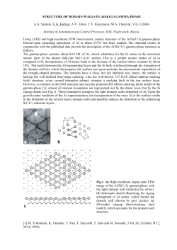


© Copyright 2026