
Publisher version
Downloaded from orbit.dtu.dk on: Jan 01, 2016 Design considerations for a digital audio Class D output stage with emphasis on hearing aid application Pracný, Peter ; Bruun, Erik; Andersen, Michael A. E. Publication date: 2013 Document Version Publisher final version (usually the publisher pdf) Link to publication Citation (APA): Pracný, P., Bruun, E., & Andersen, M. A. E. (2013). Design considerations for a digital audio Class D output stage with emphasis on hearing aid application. Technical University of Denmark, Department of Electrical Engineering. General rights Copyright and moral rights for the publications made accessible in the public portal are retained by the authors and/or other copyright owners and it is a condition of accessing publications that users recognise and abide by the legal requirements associated with these rights. • Users may download and print one copy of any publication from the public portal for the purpose of private study or research. • You may not further distribute the material or use it for any profit-making activity or commercial gain • You may freely distribute the URL identifying the publication in the public portal ? If you believe that this document breaches copyright please contact us providing details, and we will remove access to the work immediately and investigate your claim. Peter Pracný Design considerations for a digital audio Class D output stage with emphasis on hearing aid application PhD thesis, Master’s thesis, June 2013 Design considerations for digital audio Class D output stage with emphasis on hearing aid application Author(s): Peter Pracný Supervisor(s): Erik Bruun Michael A. E. Andersen Department of Electrical Engineering DTU Elektro Technical University of Denmark Ørsteds Plads, Building 349 DK-2800 Kgs. Lyngby Denmark www.elektro.dtu.dk Tel: (+45) 45 25 35 00 Fax: (+45) 45 88 61 11 E-mail: [email protected] Release date: 30 June 2013 Class: Public Edition: 1. edition Comments: This report is a part of the requirements to achieve PhD degree at Technical University of Denmark. Rights: © Peter Pracný, 2013 2 ACKNOWLEDGEMENT I would like to thank to DTU and DTU Elektro: • • • • • • • • • Prof. Erik Bruun and Prof. Michael A. E. Andersen for their supervision and for help with finding the finances to open and run this project. Ivan H. H. Jørgensen and Thomas Taul for valuable input, on-topic discussions, brain-storming sessions and help with writing of conference / journal articles. Allan Jørgensen for help and insight into IC technologies and IC design software tools. Pere Llimós Muntal and Liang Chen for cooperation and support of this project with their work. Matthias Bo Stuart, Borislav G. Tomov for discussions and input on FPGA design. Torben Poulsen and Prof. Torsten Dau for discussions and input on human hearing and sound perception. Henriette D. Wolff for finding a solution to any problem possible and for always being in the right place at the right time. Birgitte C. Viborg and Lone H. Cole for helping me with accommodation when I was in trouble. Bertil Morelli, Claus Kjærgaard and Ole C. Thomsen for help and discussions. I would also like to thank to: • • Gudmundur Bogason, Jannik H. Nielsen, Kendrick Franzen and Mohammad Shajaan for introduction to the topic of digital signal processing, sigma-delta modulators and digital IC design. Michael Deruginsky and Jannik H. Nielsen for believing in me and fighting for me. I also thank to DK Technologies A/S for being fast, flexible and very helpful company and providing the Audio Precision analyzer equipment. 3 RESUMÉ Dette projekt omhandler effektoptimering for signalbehandlingselektronikken til udgangsdelen i et audio system, dvs. interpolationsfilter, Σ∆ modulator og klasse D udgangstrin behandlet som en helhed. Der foretages en vurdering af kompromisser mellem forskellige designparametre for at nå frem til de samlede specifikationer for systemet og for at nå frem til en dybere forståelse af state-of-the-art. Der foreslås en vurderingsparameter (figure-of-merit), som muliggør en vurdering af effektforbruget i den digitale del af signalbehandlingskæden på et tidligt trin i designprocessen. Den opnående indsigt i designkompomisserne benyttes herefter til en optimering af interpolationsfilteret og system-parametrene for Σ∆ modulatoren, således at der kan opnås en minimering af skiftefrekvensen for klasse D udgangsforstærkeren, der er den mest effektforbrugende del i signalbehandlingen. • I flertrins interpolationsfilteret implementeres første trin som et half-band IIR filter opbygget af to parallelle allpass celler. En ny designmetode, der ikke kræver omfattende numeriske beregninger, foreslås til kvantisering af filterkoefficienterne. I kombination med de simple allpass celler opnås der et filter, som kræver et minimum af hardware og effektforbrug i sammenligning med state-of-the-art. • Skiftefrekvensen for klasse D udgangstrinnet reduceres til gengæld for en forøgelse af klokfrekvensen i den digitale del af signalbehandlingskæden. Herved flyttes en del af designudfordringen mht. effektforbrug fra klasse D forstærkeren til den digitale signalbehandling, hvor der kan drages fordel af skalering af IC teknologien i retning af mindre dimensioner. Denne skalering er optimeret mod digitale kredsløb. • Der vises fem design iterationer, som vurderet ud fra den foreslåede figure-of-merit resulterer i en 82% reduktion af effektforbruget i interpolationsfilteret og Σ∆ modulatoren og i en 94% reduktion af skiftefrekvensen for klasse D udgangstrinnet i forhold til den første design. • Resultatet er en digital signalbehandlingsdel, som er optimeret mht. effektforbrug og giver en lydkvalitet på niveau med state-of-the-art. Dette opnås samtidig med at skiftefrekvensen til klasse D effektforstærkeren er den laveste rapporteret i litteraturen for et Σ∆ modulator baseret system. Der foreslås fremtidigt arbejde omkring et modkoblet system med en digital Σ∆ modulator og en klasse D effektforstærker. 4 ABSTRACT ABSTRACT This work deals with power optimization of the audio signal processing back end (the interpolation filter, the Σ∆ modulator and the Class D power amplifier) as a whole. Understanding of the design parameter tradeoffs is used to derive the specifications for the back end and to understand the state-of-the-art. A figure-of-merit which allows judging the power consumption of the digital part of the back end early in the design process is proposed. The insight into the tradeoffs involved is subsequently used to optimize the interpolation filter and the system-level parameters of the Σ∆ modualtor so that the switching frequency of the Class D power amplifier – the main power consumer in the back end - is minimized. • In the multistage interpolation filter the first stage is implemented as a half-band IIR filter consisting of two parallel all-pass cells. A novel approach that does not require any rigorous numerical techniques is proposed to quantize the filter coefficients. Together with the simple all-pass cells the resulting filter has very low hardware / power demands compared to the state-of-the-art. • The switching frequency of the Class D power amplifier is reduced at the cost of the increase of the maximum clock frequency in the digital part of the back end. This approach moves the burden from the Class D power amplifier to the digital part, which easily scales with the IC technologies of today - optimized for digital design. • Judging by the figure-of-merit five design iterations are performed that lower the power consumption of the interpolation filter combined with the Σ∆ modulator by 82% and the switching frequency of the Class D power amplifier by 94% compared to the initial design. • The result is the digital part of the back end optimized with respect to power, which provides audio performance comparable to the state-of-the-art. This is combined with the lowest switching frequency of the Class D power amplifier reported in literature for the Σ∆ modulator-based digital back end. Future work for the digital Σ∆ modulator and the power amplifier with feedback is proposed. 5 TABLE OF CONTENT List of figures................................................................................................................... 9 List of tables .................................................................................................................. 13 LIST OF ABBREVIATIONS ...................................................................................... 15 1 INTRODUCTION ................................................................................................ 17 1.1 Background and motivation for research ........................................................ 17 1.2 Thesis outline .................................................................................................. 19 2 DESIGN TRADEOFFS AND STATE-OF-THE-ART ...................................... 22 2.1 High-fidelity audio back end .......................................................................... 22 2.2 Hearing-aid audio back-end ............................................................................ 25 2.3 The DPWM block and the Class D PA........................................................... 32 2.4 Design Specifications and Figure of Merit ..................................................... 34 2.5 Initial Design................................................................................................... 35 3 INTERPOLATION FILTER DESIGN .............................................................. 39 3.1 Interpolation Filter Specification .................................................................... 39 3.2 1st Stage Design .............................................................................................. 41 3.3 2nd Stage Design.............................................................................................. 49 3.4 4th Stage Design .............................................................................................. 50 3.5 3rd Stage Design .............................................................................................. 53 3.6 Summary ......................................................................................................... 53 4 DAC SYSTEM-LEVEL OPTIMIZATION ....................................................... 55 4.1 Σ∆ Modulator Order vs. OSR Tradeoff .......................................................... 55 4.2 Very High-Order Σ∆ Modulators ................................................................... 60 4.3 Using Interpolation Factor of 3 ....................................................................... 64 4.4 Increasing the Number of Quantizer Bits ....................................................... 71 4.5 Relaxing the Specification for Max. Clock Frequency................................... 76 5 CONCLUSION ..................................................................................................... 79 5.1 Results and Conclusions: Interpolation Filter ................................................. 79 5.2 Results and Conclusions: DAC....................................................................... 81 5.3 Results and Conclusions: Back End Comparison ........................................... 84 7 Table of content 5.4 Future Work .................................................................................................... 88 References ...................................................................................................................... 93 A Simulation Results ..................................................................................................... 99 B Attached Publications.............................................................................................. 106 8 LIST OF FIGURES Figure 2-1: Block schematic of a back end used in hi-fi audio application .................. 23 Figure 2-2: Optimization of the Σ∆ modulator for Class AB PA. ................................. 25 Figure 2-3: Block schematic of a back end used in hearing aid audio application ............................................................................................................. 26 Figure 2-4: Optimization of the Σ∆ modulator for Class D PA. ................................... 28 Figure 2-5: Class D amplifier with PWM using natural sampling ................................ 28 Figure 2-6: PWM sampling processes [17]. .................................................................. 29 Figure 2-7: Audio back end using PWM modulator with linear interpolation as sampling process. .................................................................................................. 30 Figure 2-8: Audio back end using hybrid PWM-Σ∆ modulator. [19] ........................... 31 Figure 2-9: A DAC with digital self-oscillating modulator........................................... 31 Figure 2-10: Current flow states in a conventional H-bridge Class D PA. ................... 32 Figure 2-11: Example of symmetric PWM with 3 bit quantizer in the SD modulator. 3 bits encode 8 levels (+3, +2, +1, 0, -1, -2, -3, -4) out of which only 7 (+3, +2, +1, 0, -1, -2, -3) are used as the signal is a sinewave symmetric around zero. ......................................................................... 33 Figure 2-12: Peak SQNR as a function of OSR for Σ∆ modulator with 3 bit quantizer of orders M = 1 – 8. ............................................................................... 35 Figure 2-13: Simplified Σ∆ modulator CRFB schematic of design used as a starting point: 3rd order modulator, OSR = 64 with 3 bit quantizer. .................... 36 Figure 2-14: NTF and STF of the Σ∆ modular of design used as a starting point. ...................................................................................................................... 36 Figure 2-1: Multi-stage IF with 4 stages performing sample-rate increase by 64. .......................................................................................................................... 39 Figure 2-2: Sound perception of (a) a normal hearing person and (b) a hearingimpaired person. The figures were originally published in [29], used with permission from Widex A/S. ................................................................................. 40 Figure 2-3: Half-band FIR filter used as the 1st stage of the IF. .................................... 41 9 List of figures Figure 2-4: IIR filter using a parallel connection of two all-pass filters. ....................... 41 Figure 2-5: Second-order all-pass filter cell. .................................................................. 42 Figure 2-6: Simplified transfer function of a half-band filter......................................... 43 Figure 2-7: IIR filter transfer function sensitivity to coefficient changes. The transfer function is most sensitive to change of the coefficient corresponding to the pole closest to the unity circle in z-domain.......................... 43 Figure 2-8: IIR filter transfer function plot in Step 1, 3 and 4. ...................................... 45 Figure 2-9: STF of the 1st stage of the IF. Specification requirement for the 2nd stage suppression is included. ................................................................................ 49 Figure 2-10: 2nd stage IIR filter transfer function plot in Step 1, 3 and 4. ..................... 50 Figure 2-11: STF of the 1st and 2nd stage of the IF. Specification requirement for the 4th stage suppression is included. ............................................................... 50 Figure 2-12: IG vs. OSRin for 4th stage filter with order = 1. Oversampling factor of 8 and 16 is used as a parameter. .............................................................. 51 Figure 2-13: IG vs. OSRin for 4th stage with orde r = 2. Oversampling factor of 8 and 16 is used as a parameter. ............................................................................. 52 Figure 2-14: STF of the 1st, 2nd and 3rd stage of the IF. Specification requirement for the 3rd stage suppression is included. ........................................... 52 Figure 2-15: IG vs. OSRin for 3rd stage with orde r of 2 and 3 as parameter. Oversampling factor of 2 is used. .......................................................................... 53 Figure 2-16: Total transfer function of the IF with oversampling by 64........................ 53 Figure 3-1: Peak SQNR as a function of OSR for Σ∆ modulator with 3 bit quantizer of orders M = 1 – 8. ............................................................................... 56 Figure 3-2: Simplified Σ∆ modulator CRFB schematic (a) 3rd order modulator, OSR = 64 and (b) 6th order modulator, OSR = 32 ................................................. 57 Figure 3-3: Σ∆ modulator NTF in the case of (red) 3rd order modulator (frequency is normalized to 64 x fsin) and (blue) 6th order modulator (frequency is normalized to 32 x fsin) .................................................................... 57 Figure 3-4: Simplified Σ∆ modulator CRFB schematic: 12th order, OSR = 16 ............. 60 Figure 3-5: Σ∆ modulator STF comparison. .................................................................. 62 Figure 3-6: Σ∆ modulator NTF comparison. .................................................................. 63 Figure 3-7: peak SQNR of the 3 bit Σ∆ modulator output signal as a function of OSR for modulator orders 1- 8. ......................................................................... 65 Figure 3-8: NTF of 6th order Σ∆ modulator with OSR = 24 and 3 bit quantizer. Maximum NTF gain Hinf as a parameter. .............................................................. 65 10 List of figures Figure 3-9: Maximum stable amplitude at Σ∆ modulator input as a function of max. NTF gain....................................................................................................... 66 Figure 3-10: peak SQNR of the Σ∆ modulator output signal as a function of max. NTF gain. ...................................................................................................... 66 Figure 3-11: Simplified schematic of the 6th order Σ∆ modulator. Design 1 is the Σ∆ modulator of Section 3.1. Design 2 is the Σ∆ modulator with OSR reduced to 24. ........................................................................................................ 67 Figure 3-12: Multistage IF. The filter of (a) performs interpolation by 32 and was used for the Σ∆ modulator in Section 3.1. Filter (b), (c) and (d) perform interpolation by 24................................................................................... 68 Figure 3-13: IIR filter using a parallel connection of three all-pass filters. .................. 69 Figure 3-14: Corresponding transfer functions to designs of Figure 3-12 (a), (b), (c), (d). ............................................................................................................ 71 Figure 3-15: NTF of 6th order Σ∆ modulator with OSR = 8 and 5 bit quantizer. Maximum NTF gain Hinf as a parameter. .............................................................. 72 Figure 3-16: Maximum stable amplitude at Σ∆ modulator input as a function of max. NTF gain. ................................................................................................. 73 Figure 3-17: SQNR of the Σ∆ modulator output signal as a function of modulator input signal amplitude and max. NTF gain Hinf. .................................. 73 Figure 3-18: Peak SQNR of the Σ∆ modulator output signal as a function of max. NTF gain. ...................................................................................................... 73 Figure 3-19: Simplified Σ∆ modulator CRFB schematic: 6th order, OSR = 8, 3 bit quan. ................................................................................................................. 74 Figure 3-20: NTF and STF of the Σ∆ modulator with order = 6, OSR = 4, 8 bit quant. ..................................................................................................................... 77 Figure 3-21: Simplified Σ∆ modulator CRFB schematic: 6th order, OSR = 4, 8 bit quan. ................................................................................................................. 77 Figure 4-1: Trading lower OSR for higher order of the Σ∆ modulator. Σ∆ modulator has larger contribution to the combined FOM (blue plot), especially at high Σ∆ modulator orders. The optimum when trading lower OSR for higher order of the Σ∆ modulator is order = 6 and OSR = 32. ............... 83 Figure 4-2: Trading lower OSR for higher number of bits in the Σ∆ modulator quantizer and higher maximum NTF gain. ........................................................... 84 Figure 4-3: ..................................................................................................................... 86 Figure 4-4: Generic integrating first order Class D feedback loop with analog input [2]. ................................................................................................................ 89 11 List of figures Figure 4-5: (a) Σ∆ modulator and Class D PA with feedback with analog input signal. (b) Σ∆ modulator and Class D PA with feedback with digital input signal and an ADC in the feedback path. (c) Σ∆ modulator and Class D PA with feedback with digital input signal and an additional SC Σ∆ modulator in the forward path. ......................................................................... 89 Figure 4-6: Σ∆ modulator with bus-splitting.................................................................. 90 Figure 4-7 (page 89 and 90): Output signal FFT of the Σ∆ modulator model using fixed-point arithmetic. 8192 points, NBW = 1.83 . 10-4 and Hann window were used for all FFT plots. Input signal is 1.4 kHz (FFT bin 512 for input) in all cases exept (g) and (h) where 1.3 kHz (FFT bin 480 for input) was used. ................................................................................................... 101 Figure 4-8: Interpolation filter model simulation using floating-point arithmetic. All FFT plots use 8192 points, NBW = 1.83 . 10-4 and Hann window. Input signal is 1.4 kHz (FFT bin 512 for input) in all cases. The interpolation filter performs interpolation by 64 (see Chapter 2) ........................ 102 Figure 4-9: Output signal FFT of Σ∆ modulator (blue plot), DPWM block (red plot) model using fixed-point arithmetic. All FFT plots use 16384 points, NBW = 9.15. 10-5 and Hann window. ................................................................. 103 12 LIST OF TABLES Table 2-1: State-of-the-art hi-fi audio DAC designs ..................................................... 23 Table 2-2: State-of-the-art hearing-aid audio DAC designs and DACs intended for mobile phones using Class D power amplifier. ............................................... 27 Table 2-3: Comparison of DAC with Class D PA using PWM..................................... 31 Table 2-4: Σ∆ modulator coefficient list of a design used as a starting point (order = 3, OSR = 64, 3 bit). ................................................................................. 36 Table 2-5: Comparison of Version 1 and Version 2 Σ∆ design. .................................... 37 Table 3-1: IIR filter coefficient values ........................................................................... 45 Table 3-2: Comparison of Design Methods and Hardware Demands ........................... 47 Table 3-3: IIR filter coefficients for Filter 2 .................................................................. 47 Table 3-4: Comparison of hardware demands in Filter 2 and Filter 3 ........................... 48 Table 3-5: IIR filter coefficients for Filter 3 .................................................................. 48 Table 3-6: IIR filter coefficients for 2nd stage. ............................................................... 49 Table 3-7: FOM of individual satges of the IF. ............................................................. 54 Table 4-1: Σ∆ modulator coefficient list (order = 6, OSR = 32, 3 bit). ......................... 58 Table 4-2: Σ∆ modulator comparison with previous design iterations. ......................... 59 Table 4-3: FOM of the individual stages of the IF and the Σ∆ modulator after the OSR reduction from 64 to 32. ......................................................................... 59 Table 4-4: Σ∆ modulator, 12th order, OSR = 16 ............................................................ 60 Table 4-5: Σ∆ modulator coefficient list (order = 12, OSR = 16, 5 bit). ....................... 61 Table 4-6: Σ∆ modulator comparison with previous design iterations. ......................... 61 Table 4-7: Σ∆ modulator coefficient list (order = 6, OSR = 24, 3 bit). ......................... 67 Table 4-8: FOM of the Σ∆ modulator and individual stages of the IF. ......................... 68 Table 4-9: Coefficients of the first stage of the IF of Figure 4-12(c) ........................... 69 Table 4-10: Back end designesign comparison ............................................................. 70 Table 4-11: Maximum clock defined by the DPWM block........................................... 72 13 List of tables Table 4-12: Σ∆ modulator coefficient list (order = 6, OSR = 8, 5 bit). .......................... 75 Table 4-13: Σ∆ modulator comparison with previous design iterations......................... 76 Table 4-14: Σ∆ modulator coefficient list (order = 6, OSR = 4, 8 bit). .......................... 78 Table 5-1: IF FOM comparison ...................................................................................... 80 Table 5-2: IFs using a stage performing interpolation by a factor of 3. ......................... 81 Table 5-3: Back end design comparison including all the blocks of the system............ 82 Table 5-4: Comparison of state-of-the-art hearing aid back end designs. ...................... 87 14 LIST OF ABBREVIATIONS ADC Analog-to-Digital Converter ASIC Aplication Specific Integrated Circuit BW Band Width CIC Cascaded Integrator Comb CT Continuous Time DAC Digital-to-Analog Converter DC Direct Current DEM Dynamic Element Matching DiSOM Digital Self-Oscillating Modulator DR Dynamic Range FIR Finite Impulse Response FOM Figure of Merit FPGA Field Programmable Gate Array FS Full Scale Hinf Maximum NTF gain of the Σ∆ modulator IC Integrated Circuit IF Interpolation Filter IG Image Gain IIR Infinite Implulse Response M Order of the Σ∆ modulator N Number of bits of the input signal NTF Noise Transfer Function OSR Over-Sampling Ratio PA Power Amplifier PDM Pulse Density Modulation PWM Pulse Width Modulation Q Number of bits in the quantizer of the Σ∆ modulator SC Switched Capacitor SNDR Signal to Noise and Distortion Ratio STF Signal Transfer Function SQNR Signal to Quantization Noise Ratio THD+N Total Harmonic Distortion + Noise USA United States of America VHDL Very High Speed IC Hardware Description Language 15 1 INTRODUCTION 1.1 Background and motivation for research Together with the advances in the semiconductor and communication industries the expectations of the users and customers are increasing as well. New products on the portable electronics market are expected to be functional at low voltages but also to consume minimum power in order to prolong their time of operation. This should also result in reduction of the battery size, weight and dimensions of the product (hearing aid, mobile phone, personal audio player, portable personal computers, …). Moreover, in competition the companies try to implement more functions (e.g. digital signal processing) in their products while keeping the recording and reproduction of the audio and video signals at high standards and delivering user-friendly control. In case of mobile phones and portable computers this product improvement is aimed mainly at consumer market. But in the case of a hearing aid, making the product comfortable and user-friendly (including lower power consumption and thus longer time of function and less weight of the battery, new functions) is even more critical since the hearing aid is in most cases indispensable for its user. Since these requirements contradict themselves from the application specific integrated circuit (ASIC) design point of view it is often difficult for the ASIC designers to keep all the product parameters within the firm specifications. It is therefore important to come up with new solutions and theories for ASIC designs and their physical implementation layouts. One of the basic functions of the portable electronic devices is the processing of the audio signal. Sound has to be converted into analog electrical signal, then it has to be digitalized, processed, turned back to analog domain and reproduced with minimal loss of quality. The back end of such a signal path is a digital-to-analog converter (DAC) and a power amplifier (PA). Both of these blocks highly influence the power consumption and quality of the reproduced sound signal in the low-voltage, low-power applications. Therefore a study is needed to be aimed at the possibilities of improvement of low-voltage, low-power DAC and PA theory and design for audio processing. 17 INTRODUCTION In the integrated low-voltage low-power audio amplifier architectures and applications of yesterday, designs with analog only interconnections were used. Moreover, complex control paths were implemented. Such architectures were not sufficiently robust, were liable to errors and wasted power consumption and chip area. Currently, in most cases a Sigma-Delta (Σ∆) DAC and DAC with PWM (Pulse Width Modulation) are used in the back-end for low-voltage low-power audio designs. A Class D switched PA usually follows the DAC. With the present increase of digitalization of the integrated architectures new possibilities arise how to improve their system designs in the future. Most important changes will be represented by the increased implementation of digital signal processing (DSP). Already today the new arising digital audio signal processing algorithms in consumer market products include surrounding noise cancellation in various environments or surround sound in headphones. Hearing aids include DSP algorithms that are able to partially make up for certain types of hearing impairment. The presence of DSP functions in tomorrow’s low-voltage, low-power audio systems / architectures opens new areas for research of new theory and design approach. The research and development will take advantage of the knowledge of the principles of quantization and digitalization, DSP theory, sound systems and acoustics / psychoacoustics making it a multidisciplinary concern. Ideally the power in a hearing aid ASIC should be spent on the DSP parts as much as possible, making the power reduction of the DAC and PA blocks of high interest. Another issue regarding the integrated circuit (IC) design is the down scaling of device dimensions to obtain higher speed when developing new technologies. In any IC design there are tradeoffs between the performance parameters which require a multi-dimensional compromise in the implementation. In the digital ICs speed is one of the most important parameters and due to the tradeoffs other parameters (e.g. current consumption) have to be sacrificed. Since the current semiconductor industry drivers are high-speed digital ICs, new technologies developed are optimized for the use in digital IC design. However in analog IC design the situation is different – speed of the IC is not always the favorite parameter. For example in the low-voltage low-power analog or mixed (analog and digital) IC designs the implementation has to operate at low bias voltages and consume minimum power in order to prolong the battery life time and minimize its weight (battery is usually the heaviest part of portable products). To be able to use as much of the small voltage headroom as possible maximum output voltage swing of the design’s blocks is also of interest. The problem arises here since for the implementation of the low-voltage low-power analog and mixed designs a technology that was optimized for high-speed digital ICs has to be used. This makes low-voltage lowpower IC design a greater challenge today and even more in the future as the technologies head toward nano-scales. Therefore it is important to investigate how the amount of analog circuits can be reduced in future low-voltage low-power IC designs leaving space for DSP implementation. 18 INTRODUCTION The purpose of this work is to design an audio back end for a hearing aid application. As was already mentioned a hearing aid is many times indispensable for a hearing impaired person and as a medical device it helps its user in their everyday life. But hearing aids can be looked at from a different point of view: hearing aids are consumer products as well. The consumers being people with hearing problems. According to the magazine The Hearing Review [1] that performs well defined surveys related to hearing problems in USA since 1984, the number of people reporting hearing loss has grown to 31.5 milion in 2004. If the trends from 1984 – 2004 continue, in 2025 there will be 41 milion of people reporting hearing loss and 53 milion in 2050. This shows a growing number of potential customers. Moreover out of the 31.5 milion of people who reported hearing problems in 2004, only 6.2 milion are hearing-aid users, leaving 24.1 milion majority in need of a hearing aid product. Future low-voltage low-power IC technologies and design approach will help to develop hearing-aids with better performance, more attractive functions and lower price, potentially targeting the majority of the growing 24.1 million customers without a hearing aid. The DAC and the PA blocks are part of this development. 1.2 Thesis outline 19 INTRODUCTION This thesis consists of five chapters which describe the hearing aid audio signal processing path back end as a whole system and its individual blocks and their power optimization – mainly the interpolation filter and the Σ∆ modulator. Chapter 1 introduces the background of the audio signal processing path back end for low-voltage low-power applications. Motivation for the research is also included. Chapter 2 focuses on the design tradeoffs involved in the audio signal processing path back end. These tradeoffs are then used to derive the specifications for the back end, to understand the state-of-the-art and to suggest an optimization strategy for the back end that is followed through the rest of the thesis. A figure-of-merit (FOM) which allows judging the power consumption of the digital part of the back end early in the design process is proposed. This chapter is partly based on a PRIME 2012 conference paper ‘ΣΔ Modulator SystemLevel Considerations for Hearing-Aid Audio Class-D Output Stage Application’ (see Appendix B for details). Chapter 3 describes the design of one of the blocks of the back end - the digital interpolation filter (IF) performing sample rate increase by 64. As the design parameters of all the blocks of the back end closely depend on each other this interpolation filter is optimized with respect to power together with the digital Σ∆ modulator and the PA in the next chapter. In Chapter 3 it is shown that an FIR filter is too power consuming to be used in a hearing-aid and an IIR filter is used instead as the first stage of the interpolation filter. To design the IIR filter with low hardware / power demands a novel technique is proposed that does not require any rigorus numerical computations. This approach provides filter designs that in some cases (see examples in Chapter 3) have almost 50% less hardware / power demands than state-of-the-art filters designed using numerical technique with genetic algorithm while fulfilling the same specification. Chapter 3 is partly based on an ICECS 2012 conference paper: ‘Interpolation Filter System-Level Considerations for Hearing-Aid Audio Class-D Output Stage Application’ and on an article submitted to IEEE TCAS-II journal: ‘Hardware-efficient implementation of Half-Band IIR Filter for Interpolation and Decimation’ (see Appendix B for details). Chapter 4 covers the system-level power optimization of the Σ∆ modulator-based DAC and its impact on the Class D PA - the main power consumer in the back end system. The switching frequency of the Class D PA is reduced at the cost of the increase of the maximum clock frequency in the digital part of the back end. This approach moves the burden from the Class D PA to the digital part, which easily scales with the IC technologies of today - optimized for digital design. This chapter is partly based on a DoCEIS 2013 conference paper: ‘System-Level Optimization of a DAC for Hearing-Aid Audio 20 INTRODUCTION Class D Output Stage’, on a PRIME 2013 conference paper: ‘System-Level Power Optimization for a Σ∆ D/A Converter for Hearing-Aid Application’ and on a paper that will be submitted to Norchip 2013 conference: ‘Interpolation by a Prime Factor other than 2 in Low-Voltage Low-Power Audio Σ∆ DAC’ (see Appendix B for details). Chapter 5 presents the results of the power optimization approach proposed in Chapter 2 and explored and performed in Chapter 3 and 4. The evaluation of the optimization process based on the FOM clearly shows that the power optimization approach results in considerable power savings in all the blocks of the back end except the block that turns the Σ∆ modulated signal to PWM. Depending on the decision for maximum clock frequency specification allowed in the back end, the power consumption of this block can either be kept unchanged or increased. If increased it results in Class D PA switching frequency as low as 88.2 kHz without sacrificing the audio performance. Either way the block that turns the Σ∆ modulated signal to PWM is digital and thus easily scales with IC technology – thus to move the operating frequency burden to digital part of the back end is a good tradeoff. To author’s best knowledge, the Class D PA switching frequency of 88.2 kHz is the lowest reported in literature for an audio digital Σ∆ modulator-based Class D PA. Such low switching frequency is in the state-of-the art works usually considered as an advantage of PWM when compared to Σ∆ modulation. This work is a proof that low Class D PA switching frequency in the range of PWM-based Class D PAs can be achieved with Σ∆ modulation. 21 DESIGN TRADEOFFS AND STATE-OF-THE-ART 2 DESIGN TRADEOFFS AND STATE-OF-THE-ART To understand a topic in engineering and design means to understand the tradesoffs being involved. Design of the DAC and PA blocks for hearing-aid audio back end is no exeption. Therefore in this section design tradeoffs are discussed. Since in general engineers of electronics are more familiar with high fidelity (hi-fi) designs, it gives sense to start the discussion of audio DACs with explanation of a DAC for hi-fi audio back-end. Then, using the tradeoffs, the DAC for hearing aid audio back end is derived. With the knowledge of the system operation and design tradeoffs the state-ofthe-art can be understood. In general the Class D PA used in the back end can be either open-loop or closed-loop (e.g. with feedback). The feedback around the Class D PA is used to correct the errors introduced by the PA. However, even without the feedback the Class D PAs can have very good performance, providing that an accurate regulated power supply is used [2] (not affordable in portable audio applications). In this section DACs combined with open-loop PA are summarized. DACs combined with PA with feedback are discussed in Section 4.4.1. 2.1 High-fidelity audio back end A block level schematic of a hi-fi audio back end can be seen in Figure 2-1. It consist of an interpolation filter (IF), a digital Σ∆ modulator, a low-precision internal DAC and a dynamic element matching (DEM) block that improves the linearity of the internal DAC. An active low-pass filter (LPF), usually implemented as switched capacitor circuit, removes the high frequency content in order not to slew the following Class AB PA. The last block is an audio LPF (speaker). When implemented as an ASIC, most of the power and chip area is consumed by the Class AB power amplifier and the active LPF. Therefore, it is these blocks that are the main focus of optimization in the case of hi-fi back end. 22 DESIGN TRADEOFFS AND STATE-OF-THE-ART Figure 2-1: Block schematic of a back end used in hi-fi audio application Table 2-1: State-of-the-art hi-fi audio DAC designs Vdd (analog/ digital) [V] Modulator DVD / CD 5/3.3 [4] ‘02 CD / mobile phone [5] ‘05 [Ref.] ‘year Application [3] ‘00 Input signal Modulator Power stage on chip [Class] SNDR [dB] DR [dB] Bits fs [kHz] OSR order Bits SNDR [dB] Digital Σ∆ 24 48 128 3 5 138 No [AB] 98 120 3.3 Digital Σ∆ 24 44.1 64 3 13 level ~ 110 No [AB] 86 98 CD / mobile phone 3.3/1.2 Digital Σ∆ 24 44.1 128 3 2 123 No [AB] 88 97 [6] ‘08 CD / mobile phone 1.8 Digital Σ∆ 24 48 64 2 8 117 Yes [AB] 97 108 [7] ‘08 Mobile phone 1 Digital Σ∆ 16 44.1 64 3 3 106.7 Yes [AB] 82 90 [8] ‘09 Mobile phone 0.8 Digital Σ∆ 16 48 64 3 3 107 Yes [AB] 69 88 There are number of static and dynamic parameters to characterize a DAC [9]. Since a Σ∆ modulator is a dynamic system, only dynamic parameters can be applied. In state-of-the-art works it is mostly signal-to-quantization-noise ratio (SQNR), signal-tonoise-and-distortion ratio (SNDR) and dynamic range (DR) that are reported. Summary of published state-of-the-art works with high impact, dealing with hi-fi audio DAC designs can be seen in Table 2-1. In the case of hi-fi back end, the input signal is usually quantized with 16 bits and sampled at 44.1 kHz or quantizer with 20 - 24 bits and sampled at 48 or 96 kHz. In ideal case the 16 bit quantization leads to SQNR = 6,02 . 16 + 1,78 = 98 dB [9] at full scale (FS) input signal. The 20 bit quantization leads to SQNR = 6,02 . 24 + 1,78 = 122 dB at full scale input signal. For ideal 24 bit quantization SQNR = 146 dB. 23 DESIGN TRADEOFFS AND STATE-OF-THE-ART DR of a DAC is a ratio of the largest signal level the converter can handle and the noise level and determines the maximum SNDR. In order to reproduce the audio signal without significant loss of quality the hi-fi DACs target DR between 98 - 110 dB (see Table 2-1) at the total output of the system for applications such as compact disc (CD) quality playback or mobile phone. In the case of digital versatile disc (DVD) quality, the highest DRs reported in literature are around 120 dB. This means that the SQNR = 146 dB at the input can not be reproduced. In such case, if audio quality is of high importance, the higher the DR the better. Of course there will be a tradeoff and the designer will pay with high power consumption and large chip area – parameters that can be afforderd in home audio decks. The Σ∆ modulator that is one of the building blocks follows the same tradoffs. The Σ∆ modulator has three main system level parameters reported in literature: the oversampling ratio (OSR), the order and the number of bits in its quantizer [10]. From Table 2-1 it can be seen that in the case of mobile phone / CD quality, the Σ∆ modulator targets around 110 – 120 dB peak-SQNR at its output. In the case of DVD quality, the Σ∆ modulator targets around 138 dB peak-SQNR at its output. Thus in both cases the performance is better than needed at the total output of the system. The Σ∆ modulator is designed in this way, because power consumption is not as much an issue in hi-fi application and audio quality is the preferred parameter. Moreover, the main power consumers are the analog Class AB power amplifier and the active LPF, not the digital Σ∆ modulator. Since the digital part of the system is way less power and area demanding it can be afforded to design the digital blocks with overhead if possible [6], this is also the case of the Σ∆ modulator. Usually it is preffered to have the digital part and the analog part on two separate chips in order to prevent interference from the digital noisy part into the analog part. Again the two-chip solution requires more area. This is not as much a problem in large home audio decks. Therefore, to reach certain peak-SQNR at the output of the Σ∆ modulator in hi-fi back end it is preferred to: • • 24 Keep the order low, as high order Σ∆ modulator results in high slope of the outof-band noise which might be difficult to filter out. With high order Σ∆ modulator part of the noise slope can remain present after the low-pass filtering, which would decrease the SNDR at the total output of the system – a preferred parameter. (see Figure 2-2a) Increase the OSR (= increase the operation frequency of the Σ∆ modulator) as the power consumption of the digital Σ∆ modulator is not the limiting parameter. Moreover for a set peak-SQNR performance, higher OSR helps to reduce the problems with the low-pass filtering – one of the main power consumers in the system. (see Figure 2-2b) DESIGN TRADEOFFS AND STATE-OF-THE-ART • Increase the number of bits in the Σ∆ modulator quantizer as it reduces the outof-band noise and thus helps to reduce the problems with the low-pass filtering. The number of bits is usually kept under 5 because with higher number of bits the DEM block becomes complicated. The choices of the Σ∆ modulator system-level parameters in the state-of-the-art DAC designs intended for hi-fi applications follow this approach (see Table 2-1). (a) (b) Figure 2-2: Optimization of the Σ∆ modulator for Class AB PA. 2.2 Hearing-aid audio back-end The hearing-aids of today are devices where strict specifications are applied. Sufficient audio quality and the need for longer operation time combined with the desire to shrink the size of the hearing-aid devices to make it virtually invisible leaves less space for the battery and integrated circuits. These demands contradict each another, making the current consumption of the electronics inside the hearing-aid one of the crucial parameters for the design. To find the optimum balance between the design parameters in every part of a hearing-aid device is therefore of vital importance. This includes the back end of the audio signal processing path. The parameters of high interest are low power consumption and small chip area, resulting in longer operation time and smaller battery size. The audio quality is the parameter to be compromised. A block level schematic of a audio back end used in hearing-aid can be seen in Figure 2-3. 25 DESIGN TRADEOFFS AND STATE-OF-THE-ART Figure 2-3: Block schematic of a back end used in hearing aid audio application The input signal in hearing aid application is usually quantized with 16 bits, resulting in SQNR = 98 dB. The input sampling frequency is half compared to hi-fi fsin = 44.1 / 2 = 22.05 kHz, targeting the audio bandwidth (BW) of 10 kHz. To lower the high power consumption of the Class AB PA and to eliminate the expensive active on-chip analog LPF used in hi-fi back end of Figure 2-1, the hearingaid back end uses Class D PA instead and the LPF is external passive LC filter [11], [12]. This way the whole analog part of the hi-fi back end is avoided, saving power consumption and chip area. Still the Class D power amplifier is the largest power and chip area consumer in the system and introduces more distortion than the Class AB PA. As was already mentioned the audio quality is the parameter to be compromised in a hearing aid. The Class D power amplifier operates in switched mode. A basic Class D PA is in Figure 2-3. It consists of two low-ohmic switches that connect the output node to the positive or negative supply rail. To avoid two supply rails and have single supply operation the PA is usually implemented as an H-bridge (see Section 1.3). Class D PAs achieve efficiency which is typically above 90% at full output power. The efficiency is largely determined by two factors [2]: switch impedance and switching frequency. Finite switch impedance causes conductive losses that are proportional to the square of the output current and is usually the limiting factor for efficiency at full power. At low output power, switching losses are the dominant factor. For each output transistion, the input capacitance of the switch devices needs to be charged/discharged, causing charging losses that are proportional to input capacitance and switching frequency. Moreover, finite switching speed causes energy loss during each output transistion. Switch impedance is inversely proportional to the size of the switch device, whereas input capacitance linearly scales with size. For high efficiency, the switching frequency must be as low as possible, whereas the switch device size should be optimized to tradeoff conductiong and charging losses. An important difference compared to the Class AB PA is that in the case of Class D the switching frequency of the power amplifier and thus its efficiency 26 DESIGN TRADEOFFS AND STATE-OF-THE-ART depends on the OSR of the Σ∆ modulator. Thus lower OSR in the Σ∆ modulator is preferred. Just like in the case of hi-fi back end, a digital Σ∆ modulator is used and due to the oversampling nature of the Σ∆ modulator an IF is needed prior to the modulator. In the case of a multi-bit Σ∆ modulator a digital pulse width modulation (DPWM) block is needed to be able to connect the Σ∆ modulator to the Class D power amplifier. The DPWM block turns the multi-bit output signal of the Σ∆ modulator into 1 bit (2 level) symmetric pulse width modulation signal that operates the switch devices of the PA. The choices of the Σ∆ modulator system-level parameters reported in literature in the state-of-the-art back end systems intended for hearing-aids and mobile phone DACs using Class D power amplifier can be seen in Table 2-2. Table 2-2: State-of-the-art hearing-aid audio DAC designs and DACs intended for mobile phones using Class D power amplifier. Vdd (analog/ digital) [V] Modulator Bits fs [kHz] OSR order Bits SNDR [dB] Power stage on chip [Class] Hearing aid 0.9 Digital Σ∆ 16 32 64 4 1 N/A Yes [D] 79 N/A [14] ‘09 Mobile phone 1.2 Digital Σ∆ 16 44.1 64 3 3 106.7 No [D] 90 N/A [15] ‘09 Mobile phone 3.6 Digital Σ∆ 24 48 48 3 7 122 Yes [D] N/A N/A [16] ‘10 Hearing aid 1.8 Digital Σ∆ 16 22.05 64 4 1 105.7 Yes [D] 85.6 90 [Ref.] ‘year Application [13] ‘07 Input signal Modulator SNDR [dB] DR [dB] It is interesting to note that the state- of-the-art Σ∆ modulator design approach for back end with Class D power amplifier seems to be the same as in the case of back end with Class AB power amplifier in most cases. The only difference is the use of 1 bit quantizer in hearing-aid Σ∆ modulator that allows the designers to remove the DPWM block and operate the PA directly with the output of the SD modulator. Moreover Σ∆ modulator with 1 bit quantizer causes stability problems and reduces maximum stable ampitude (MSA) at the input of the Σ∆ modulator – a crucial parameter in hearing aid. Noting again that the switching frequency of the Class D power amplifier depends on the OSR of the Σ∆ modulator it gives sense to ask wheter the Σ∆ modulator systemlevel parameters can be better optimized for low-power low-voltage operation. Therefore, to reach given peak-SQNR at the output of the Σ∆ modulator in hearing-aid back end following approach will be investigated in this work: 27 DESIGN TRADEOFFS AND STATE-OF-THE-ART • Decrease the OSR (= decrease the operation frequency of the Σ∆ modulator) as this lowers the switching frequency of the Class D power amplifier – the main power and chip area consumer in the system. The price to pay is that lower OSR will result in more noise left after the low-pass filtering, which might decrease the quality of the output signal – a parameter that is being compromised (see Figure 2-4a). • Increase the order of the Σ∆ modulator. In order to keep given peak-SQNR at the Σ∆ modulator output, the order has to be increased since the OSR is decreased (see Figure 2-4b). • Increase the number of bits in the Σ∆ modulator quantizer as it helps with the stability of the high-order Σ∆ modulator. (a) (b) Figure 2-4: Optimization of the Σ∆ modulator for Class D PA. Figure 2-5: Class D amplifier with PWM using natural sampling There are other types of modulators used for Class D PAs in low-voltage lowpower applications using PWM modulation and its variants. A Class D system with PWM modulation can be seen in Figure 2-5. The main advantage of PWM modulation is its simplicity, compared to Σ∆ modulation it does not need oversampling and thus has tendency to dissipate less power as the Class D PA switches at lower frequency. The quality of the audio signal at the output depends on the type of sampling used. 28 DESIGN TRADEOFFS AND STATE-OF-THE-ART Figure 2-6: PWM sampling processes [17]. There are three types of sampling processes that are considered in literature: natural sampling, uniform sampling, algorithmic sampling (using linear and other types of interpolation) (see Figure 2-6). The lowest total harmonic distortion (THD) would be obtained using natural sampling. The problem with natural sampling is that it reqires analog sampling process for precise sampling and is hence impractical to realize in digital domain. This is because the amplitude of the input modulating signal at the intersection with the carrier waveform must be known. Put differently, for a true digital natural sampling emulation, the complete contour of the input modulating signal needs to be known, that is the input modulating signal must be sampled at infinite rate [17]. The uniform sampling process, on the other hand is highly simplistic PWM process. But as the pulsewidth arising from the sampled points differs considerably from the ideal natural sampling pulsewidth, high THD compared to Σ∆ modulation is a result (2% THD reported in [17] for PWM with uniform sampling compared to 0.08% for Σ∆ modulation). Despite the fact that in the case of PWM the THD is higher, it is still well within the audio specification. In order the THD to be hearable it has to reach 10%. The uniform sampling process involves generation of digital pulses from a digital counter clocked at a rate of 2N . fsin (where N is the number of bits used for input signal quantization). With 16 bit signal at the input, the clock reaches Giagaherz range which is impractical [18]. The algorithmic sampling using linear interpolation [17] (see Figure 2-6) is still simple and approximates the natural sampling better than uniform sampling. The THD reported is in the range that is achieved with Σ∆ modulation. With N = 16 bit input signal 29 DESIGN TRADEOFFS AND STATE-OF-THE-ART Figure 2-7: Audio back end using PWM modulator with linear interpolation as sampling process. sampled at 48 kHz, the clock needed for the digital counter in the pulse generator in [17] is (211 . 48 kHz) / 2 = 50 MHz (see Figure 2-7). Compared to usuall 5 – 8 MHz clock needed in Σ∆ modulation this is very high / unacceptable. The factor 211 would normally be 216 but the clock counter in [17] is equipped with noise-shaper which reduces this factor. The division by 2 is because of the clock doubler used in the pulse generator. The high frequency operation and added hardware make the pulse generator the most power demanding block. The power dissipation distribution in this system is 88% for the pulse generator and 12% for the rest of the circuit (including the Class D PA). Thus the main focus of optimization in this system will be the main power consumer – the pulse width generator. Therefore the optimization approach taken tries to lower this frequency [19]. To address this issue the number of bits N converted by the pulse generator needs to be lowered without the loss of audio quality. To perform this, a Σ∆ modulator is used, resulting in a hybrid of PWM using algorithmic sampling and Σ∆ modulation [19] (see Figure 2-8). In this case the sampling process is 2nd order Lagrange interpolation which requires the input signal to be upsampled by a factor of 2 with an interpolation filter. The Σ∆ modulator of this sytem also takes advantage of this upsampling. In the end the pulse generator clock is lowered to 12.3 MHz with THD equivalent to pure Σ∆ modulation and the Class D PA swiching frequency 96 kHz (doubled compared to [17] because of the IF). In total this hybrid design is reported to consume 50% of power compared to [17] (Figure 2-7) despite the fact that the switching frequency of the Class D PA is doubled. Also the power consumption was re-distributed, 3% for the pulse generator, 97% for the rest of the circuit, showing that the main power consumer of Figure 2-7 was optimized. Summary of [17] and [19] can be found in Table 2-3. 30 DESIGN TRADEOFFS AND STATE-OF-THE-ART Figure 2-8: Audio back end using hybrid PWM-Σ∆ modulator. [19] Table 2-3: Comparison of DAC with Class D PA using PWM input [Ref.] Σ∆ Modulator THD+N Sampling Class D Switching freq. [kHz] OSR order bits [dB] 48 - - - -66 96 2 3 8 -74 ‘year BW [kHz] fs [kHz] Bits process [14] ‘05 4 48 16 linear [15] ‘09 8 48 16 2nd order Lagrange For completnes it needs to be mentioned that in the case of PWM modulation the modulator could be implemented as a digital self-oscillating modulator (DiSOM) [20], [21] (Figure 2-9). Figure 2-9: A DAC with digital self-oscillating modulator. The idea of DiSOM was originally porposed for a DC-DC converter and the advantage of this structure would be that it does not need clock for generating the carrier signal. An audio DAC with DiSOM modulator has not been reported yet in literature so it is hard to compare what the audio quality of such simple structure would be. Analog implementations of self-oscillating drivers for Class D PA report 0.1 % THD + N [22]. In case such result would be confirmed for digital inpmlementation of self-oscillating modulator this would be highly competitive structure with Σ∆ modulator. The 0.1 % THD+N in analog implementation however was obtained with a feedback loop taken from the output of the LPF back to the modulator input. In the case of digital implementation, this would require an analog-to-digital converter (ADC) in the feedback path, making the structure more complex and less attractive. On the other hand without the 31 DESIGN TRADEOFFS AND STATE-OF-THE-ART feedback the THD+N result would be worse. Simulations are needed to be performed for comparison with Σ∆ modulation. In state-of-the-art works the fact that the Σ∆ modulation is more oriented towards audio performance and requires oversampling and thus comsumes more power, is used as the main argument why a designer should prefer PWM modulator in low voltage low power audio application. However the Σ∆ modulators assumed in comparisons with PWM modulators in published woks [17], [19] are unneccesarily complex – such as 4th (or higher) order Σ∆ modulator with OSR = 128 or 256 and 3 bit or 4 bit quantizer and thus the comparison is biased. Moreover, as was shown in [19], a Σ∆ modulator is used with PWM in order to lower the maximum clock frequency. A hybrid DAC is a result. This shows that the potential of Σ∆ modulators in low voltage low power audio applications has not been fully utilized. For this reason this work starts with optimization of a Σ∆ modulator for low voltage low power audio application - a hearing aid. Only after such optimization has been performed a proper comparison can be done. Since the optimization performed at system-level has the largest impact on system performace, including the power consumption, it will be the main focus of this work. 2.3 The DPWM block and the Class D PA In case a multibit quantizer is used in the Σ∆ modulator the DPWM block turns the Σ∆ modulator output into 1 bit signal. The 1 bit signal then operates the switches of the Class D PA. The Class D PA is usually operated in differential manner and is implemented as an H-bridge (Figure 2-10). Figure 2-10: Current flow states in a conventional H-bridge Class D PA. 32 DESIGN TRADEOFFS AND STATE-OF-THE-ART (a) (b) Figure 2-11: Example of symmetric PWM with 3 bit quantizer in the SD modulator. 3 bits encode 8 levels (+3, +2, +1, 0, -1, -2, -3, -4) out of which only 7 (+3, +2, +1, 0, -1, 2, -3) are used as the signal is a sinewave symmetric around zero. With an H-bridge both sides of the load (loudspeaker) are driven in opposite phase which allows operation from single supply and doubling the voltage swing across the load e.g. four times more output power than single ended Class D PA. The disadvantage compared to single ended solution is that with the H-bridge the number of switches (and inductors) is doubled. Also H-bridge needs two 1 bit inputs, input P and input N (Figure 2-11), and thus two DPWM blocks to generate these 1 bit signals. The signal across the load is symmetric PWM obtained as a difference of the P and N signals. With symmetric PWM (P – N in Figure 2-11) the H-bridge is in one of the three states in Figure 2-10: +1, 0, -1. The amount of differential-mode high frequency energy is reduced compared to a case when the H-bridge operates in two states only (+1, -1). This reduces the demands on the output filter to an extent that the filter might not be needed and the low-pass filtering can be performed by the speaker itself, provided that the speaker is close to the PA output, which is usually the case in hearing aids and portable audio applications [2], [23], [24], [25]. The hearing aids are usually biased from a zinc-air battery. The battery voltage is most of the operation time of the hearing device around 1.2V and the impedance of the speaker varies from 10Ω to 300Ω. Bias voltage of 1.2V is also used in state-of-theart hearing aid back end in [26]. With 97% efficiency achieved and 160Ω load imped- 33 DESIGN TRADEOFFS AND STATE-OF-THE-ART ance in [26] the power delivered to the load is only 1.14 mW. This leads to a conclusion, that in order to provide higher output power that is needed in a hearing aid, it is needed to bias the Class D PA from a regulated power supply higher than the battery voltage. 2.4 Design Specifications and Figure of Merit Taking into account that a hearing-aid is intended for people with hearing problems the bandwidth of the audio signal is a trade-off between ensuring sufficient sound quality and the limited power available and is normally around 10 kHz. In order to fulfill the Nyquist criterion the sampling frequency at the input of the back-end system is fsin > (2 . BW) = 20 kHz. In the case of this work half of the regular high fidelity sampling frequency 44.1 kHz / 2 = 22.05 kHz is used. Also in this work ideal 16 bit quantization of the back-end system input signal is assumed. This results in SQNR = 98 dB. The input signal of the back end is then up-sampled using a multistage IF and passed to the Σ∆ modulator. Another requirement in this work is the SNDR at the total output of the backend of 90 dB. The IF and the Σ∆ modulator are designed to keep the quality of the audio signal close to SNDR = 98 dB so that a margin of approx. 8 dB is left for the performance reduction introduced by the output stage. The MSA at the Σ∆ modulator input is also a crucial parameter in hearing-aids. In this work MSA as close to -1 dBFS as possible is a target. Maximum system clock frequency should be 5.6 MHz. Both the IF and the Σ∆ modulator are digital designs in this work. A digital Σ∆ modulator can be looked at as a digital filter with two transfer functions: a signal transfer function (STF) and a noise transfer function (NTF). This allows to adopt the idea for a figure of merit (FOM) from [27] [28], used for digital filters and judge the complexity of both, the IF and the Σ∆ modulator, by counting the number and complexity of adders. This leads to FOM = Σi (bi . OSRi) (Eq. 1) Where i is the number of adders in the block of interest, bi is the number of bits used in individual adders and OSRi is the oversampling used for the individual adders. In the case of the Σ∆ modulator block OSRi is the same for all the adders. Since this FOM accounts for the majority of the cells needed to implement the IF and the Σ∆ modulator it is roughly proportional to the power consumption of the design and is a valuable tool when choosing between designs at early design phase. The lower the FOM the less hardware and power demanding the design is. There are more precise 34 DESIGN TRADEOFFS AND STATE-OF-THE-ART figures of merit for Σ∆ modulators used in other works [10]. However these figures of merit can be used only after the design has been completed and possibly measured. The advantage of the figure of merit of Eq. 1 is that it allows to decide early in the design process whether or not an optimization approach is reasonable. The above mentioned specifications and FOM will be used in this work for comparison when optimizing the back end system. For the sake of comparison all the FOMs in this work are normalized to 64 . fsin = 64 . 22.05 kHz = 1.4 MHz. 2.5 Initial Design Figure 2-12: Peak SQNR as a function of OSR for Σ∆ modulator with 3 bit quantizer of orders M = 1 – 8. The starting point for the Σ∆ modulator design in this work is the combination of system level parameters that are reported in most of the state of the art designs in Table 2-2: 3rd order modulator with OSR =64, 3 bit quantizer. The maximum modulator noise transfer function (NTF) gain is Hinf = 1.5 as advised in [10]. A plot of peak SQNR that the modulator can achieve as a function of OSR for modulator orders of 1 to 8 can be found in Figure 2-12. This figure shows that the chosen combination of system level parameters provides peak SQNR = 106 dB. However SQNR = 98 dB only is required at the modulator output according to the specification. This means that a margin of 106 – 98 = 8 dB is left. This margin can be used for reducing hardware / saving power in the Σ∆ modulator. To confirm, the Σ∆ modulator is designed in two versions. In Version 1 the peak SQNR performance of the Σ∆ modulator is kept after the coefficient quantization close to the ideal 106 dB. In Version 2 the peak SQNR at the modulator output is reduced to 98 dB according to the specification and the margin of 106 – 98 = 8 dB is used to obtain coarse coefficient quantization. List of the quantized coefficients for both modulator versions can be seen in Table 2-4. The modulator structure used is cascade of resonators with feedback (CRFB) and can be seen in Figure 2-13. The NTF and the STF of the Σ∆ modulator is in Figure 2-14. 35 DESIGN TRADEOFFS AND STATE-OF-THE-ART Table 2-4: Σ∆ modulator coefficient list of a design used as a starting point (order = 3, OSR = 64, 3 bit). Quantization Version 1 Version 2 Coeff. Value Shift/Add Adders Shift/Add Adders a1 1/8 2-3 0 2-3 0 a2 0.3446 2-2+2-4+2-5 2 2-2 0 a3 0.3941 2-2+2-3+2-6 2 2-2+2-3 1 -3 -3 b1 1/8 2 0 2 0 c1 1/2 2-1 0 2-1 0 c2 1/2 2-1 0 2-1 0 c3 1.4063 20+2-2+2-3+2-5 3 20+2-2 1 g1 0.0029 2-9+2-10 1 2-9 0 Figure 2-13: Simplified Σ∆ modulator CRFB schematic of design used as a starting point: 3rd order modulator, OSR = 64 with 3 bit quantizer. Figure 2-14: NTF and STF of the Σ∆ modular of design used as a starting point. 36 DESIGN TRADEOFFS AND STATE-OF-THE-ART Table 2-5: Comparison of Version 1 and Version 2 Σ∆ design. Peak-SQNR [dB] Modulator Order Quant. bits OSR FOM Adders ideal quantized 3 3 64 18 106 106 (Version 1) 296 3 3 64 12 106 98 (Version 2) 193 A model using fixed-point arithmetic was designed in Matlab and simulated. The Matlab model is provided on a USB-key attached with this work. Simulation results are provided in the summary in Appendix A. The fixed-point model performs computations exactly as a VHDL code does (there is one-to-one correspondence of the output bit-stream of the Matlab model and the VHDL code) and thus it can be used for judging the complexity of the design. Comparison of Version 1 and Verion 2 using the FOM of Eq.1 can be seen in Table 2-5 clearly showing better FOM (e.g. less hardware / power consumption) for Version 2 where the modulator performance is overdesigned and the margin gained is subsequently used for coarse coefficient quantization. This approach will be used in for other designs in this work. 37 3 INTERPOLATION FILTER DESIGN 3.1 Interpolation Filter Specification As was already mentioned, due to the oversampling nature of Σ∆ modulators an IF is needed prior to the modulator. Since the Σ∆ modulator in the initial design in Section 1.5 works with OSR = 64 the IF has to increase the input sampling frequency fsin 64 times. To reduce the hardware demands and power consumption, the state-of-theart DAC designs implement the IF as a multi-stage filter [10]. The IF that is used for the initial Σ∆ modulator design of Section 1.5 (order = 3, OSR = 64, 3 bit, max. NTF gain = 1.5) consists of 4 stages and can be seen in Figure 3-1. Ideal 16 bit quantization is used for the input signal of the IF. This gives SQNR = 98 dB at the filter input with full scale signal. The filter is designed to keep the audio quality so that SQNR close to 98 dB is still available at its output. Figure 3-1: Multi-stage IF with 4 stages performing sample-rate increase by 64. In [10] it is proposed to use the Σ∆ modulator NTF (Figure 2-14 in this case) to decide the suppression needed in the stop-band of individual stages of the filter. Ideally the images in the frequency spectrum should be suppressed below the NTF of the Σ∆ modulator. It is not necessary to suppress the images even more as the Σ∆ modulator will introduce the amount of noise defined by NTF anyway. The NTF of the Σ∆ modulator in Figure 2-14 suggests that to bring the far images below the NTF it is not needed to use difficult filters for the last stages, as suppression of around 30 dB only is needed and the transition band allowed is wide. This is why cascaded-integrator-comb (CIC) filters can be used as a 3rd and 4th stage. The NTF also suggests that the most hardware 39 INTERPOLATION FILTER DESIGN demanding stage will be the first stage. With the bandwidth of 10 kHz, to bring the closest image in the spectrum below the NTF, a suppression of -96 dB is needed in the stop-band for the first filter stage. This will result in a high filter order. To lower the hardware demands of the first stage the graphs of Figure 3-2(a) can be used. Here it can be seen that in the case of normal hearing person, if the speech input signal of normal intensity is suppressed around 60 dB it will reach the threshold of hearing. (a) (b) Figure 3-2: Sound perception of (a) a normal hearing person and (b) a hearing-impaired person. The figures were originally published in [29], used with permission from Widex A/S. Figure 3-2(b) suggests that the specification of the stop-band attenuation could be lowered even further as the threshold of hearing for hearing-impaired person is raised. However, the amount of hearing loss varies among the hearing-aid users. To assure sufficient sound quality for all the hearing-aid users the specification for the stop-band attenuation is defined by the attenuation needed for least hearing impaired hearing-aid users (e.g. close to normal hearing person). For this reason the specification of 58 dB stop-band suppression is used in this work. When deciding the pass-band ripple of the whole filter chain note that 1 dB ripple is audible and 0.1 dB ripple is used for high fidelity audio application. Since a hearing aid is a battery operated device the hardware demands and current consumption needs to be limited. Therefore pass-band ripple of 0.5 dB is chosen for the whole filter chain as a specification out of which 0.1 dB is allocated for the first stage of the filter. The remaining 0.4 dB cover the pass-band droop that will be introduced by the CIC filters. 40 INTERPOLATION FILTER DESIGN 3.2 1st Stage Design With the first stage of the IF implemented as a half-band FIR filter, the first stage becomes the most hardware demanding of all filter stages [10]. The half-band FIR filter can be seen in Figure 3-3. A model using fixed-point arithmetic was designed in Matlab. The Matlab model performs digital operations exactly as the VHDL code does. The VHDL design is implemented on a Spartan 6 FPGA and masured with an audio analyzer. The delay line is implemented as a RAM memory and the coefficents are stored in ROM memory. The order of this filter is 74, reaching 60 dB suppresion in the stop-band. Due to the fact that half of the coefficents in a half-band filter is zero and due to symmetry of the filter only 19 filter coefficients have to be stored in the ROM. The input signal of the filter is quantized with 16 bits, the coefficients are quantized with 18 bits. The filter performs 19 multiplications per input sample. This is equivalent to 342 18-bit adders needed per input sample which means that this is a very hardware demanding filter mostly because of the use of a shared multiplier and can not be afforded in a hearing-aid. Figure 3-3: Half-band FIR filter used as the 1st stage of the IF. To reduce the hardware demands and power consumption, half-band IIR filter can be used instead if the requirement for phase-linearity is not strict [30]. Design optimization using a poly-phase IIR structure of all-pass filters for sample-rate conversion was originally proposed in [31]. Such IIR filter performing interpolation by factor of 2 can be seen in Figure 3-4. Figure 3-4: IIR filter using a parallel connection of two all-pass filters. 41 INTERPOLATION FILTER DESIGN Figure 3-5: Second-order all-pass filter cell. The all-pass transfer functions H0(z-2), H1(z-2) are cascade of second-order cells that can be seen in Figure 3-5. The transfer function of these cells is an all-pass function Hi(z-2) that can also be seen in Figure 3-5 Thorough description of this type of filters was provided in [30] and a genetic algorithm was used to design such filter in [32]. Various options for the all-pass IIR filter cells and sensitivity to coefficient quantization can be found in [27] and [28]. To reduce the hardware demands in the IIR filter the state-of-the-art works focus on filter coefficients and their implementation as sum of integer powers of two. This allows the coefficients to be implemented using shifters and adders / subtractors only, avoiding multipliers. Since shifts can be implemented simply by re-wiring individual bits of a binary word they do not consume any hardware. Thus the complexity of the filter in the state-of-the-art works such as [27], [28] is judged by counting the number of adders needed to implement the coefficients. In next sections the optimization methods in the state-of-the-art works are discussed and a step-by-step method that does not involve any rigorous numerical technique is proposed. The proposed method results in considerable hardware savings. Example designs are included. 3.2.1 Filter Design Methods Discussion A transfer function of a half-band poly-phase IIR filter as a parallel connection of two all-pass filters can be seen in Figure 3-6. Where ωp, ωs, δp, δs are normalized pass-band and stop-band cut-off frequency and pass-band and stop-band ripple respectively. Per symmetric properties of half-band filter ωp = 1 - ωs and δp ~ δs2/2 [31]. The approach chosen to design and minimize the IIR filter in the state-of-the-art works is following [27]: Given ωp, ωs, δp, δs it is needed to find the orders of the parallel all-pass filters so that the criteria given are met after the filter coefficients are quantized and implemented using shifters and adders / subtractors only, avoiding multipliers. In order to find the combination of the quantized coefficients using the lowest number of adders so that the filter meets the criteria a genetic algorithm is used. 42 INTERPOLATION FILTER DESIGN Figure 3-6: Simplified transfer function of a half-band filter. Figure 3-7: IIR filter transfer function sensitivity to coefficient changes. The transfer function is most sensitive to change of the coefficient corresponding to the pole closest to the unity circle in z-domain. In [28] it is shown that the sensitivity of the coefficients increases as, in zdomain, the position of the pole corresponding to a coefficient gets closer to the unity circle. The largest of the coefficients then corresponds to the pole closest to unity circle. To briefly illustrate this effect see Figure 3-7 where a transfer function of a half-band IIR filter using a parallel connection of two all-pass filters is plotted (red plot). The filter coefficients can be seen in Table 3-1 (Step 1 column). The largest of the coefficients a1,3 corresponds to the pole closest to the unity circle. The smallest of the coefficients a0,1 corresponds to the pole furthest from the unity circle. If coefficient a1,3 is changed by 1% while leaving the other coefficients unchanged the transfer function changes (blue plot) compared to the original. The same can be repeated with coefficient a1,2 (green plot) and a0,1 (black plot). From Figure 3-7 it can be seen that the IIR filter transfer function changes the most with coefficient a1,3 changed by 1% and changes the least with coefficient a0,1 changed by 1%. Performing similar investigations on other filters of any order will also reveal that the largest coefficient is the most sensitive and has the potential to consume largest number of adders of all the coefficients when quantized. 43 INTERPOLATION FILTER DESIGN For detailed study of coefficient sensitivity and use of all-pass filter cells that are more resistant to coefficient quantization refer to [28]. With [27], [28], [32], [33] focused on minimizing the number of adders in the coefficients, the all-pass filter cells resistant to coefficient quantization do result in lower amount of adders in coefficients, but at the expense of more complex cell structure than the one in Figure 3-5. For this reason judging the filter complexity only by counting the number of adders in the coefficients as in [27], [28], [32], [33] is not complete. To overcome the above mentioned problems different method to minimize the IIR filter hardware demands is proposed next. The complexity of the resulting IIR filter is judged by counting all the adders in the filter: 3.2.2 Proposed Filter Design Method with Example Design Three filter design examples are provided. Filter 1 is used to explain the stepby-step design method that does not involve any rigorous numerical technique and results in considerable hardware savings compared to the state-of-the-art. Filter 2 and Filter 3 are used as a comparison of the proposed method to current state-of-the art designs of [27] and [33] where numerical optimization methods are used. These filters are designed for interpolation purpose but because of the duality the same coefficients can be used for filters performing decimation. Filter 1: In this example the first stage of the multistage filter in Figure 3-1 is designed as a parallel connection of two all-pass filters performing sample rate increase by a factor of 2 (see Figure 3-4) and optimize it with respect to hardware demands. The all-pass cell of Figure 3-5 is used. As was already mentioned hearing aids have normally a bandwidth of BW = 10 kHz. To fulfil the Nyquist criterion the input sampling frequency in this example is half of the standard hi-fi audio sampling frequency fsin = 44.1 kHz / 2 = 22.05 kHz. The interpolation factor is 2 so the output sampling frequency fsout = 44.1 kHz. Thus normalized pass-band cutoff frequency ωp = (2.π.10 kHz) / (π.44.1 kHz) = 0.4535. Per symmetry of half-band filter ωs = 1 – ωp = 0.5465 and normalized transition band ωt = ωp ωs = 0.093. From the IF specification the pass-band ripple is chosen 0.5 dB for the whole filter chain in Figure 3-1, out of which δp = 0.1 dB is allocated for the half-band IIR filter. Per Figure 3-2 the stop-band ripple δs = -58 dB is sufficient suppression for hearing-aid application. 44 INTERPOLATION FILTER DESIGN Step 1: Given ωp = 0.4535, δp = 0.1 dB , δs = -58 dB, input sampling frequency fsin = 22.05 kHz, the sampling-rate alteration ratio of 2, the half-band IIR filter is designed according to Figure 3-4 with all-pass sections of Figure 3-5. The analytic design method in [31] gives the transfer function in Figure 3-8 (red plot) and the coefficients in Table 3-1 Step 1 column. Note that the stop-band ripple is more than necessary (-80 dB) at this point, which will aid the coarse coefficient quantization later in Step 4. Figure 3-8: IIR filter transfer function plot in Step 1, 3 and 4. Table 3-1: IIR filter coefficient values Coefficient Step 1 Step 3 Step 4 Shift/Add Adders a1,3 0.9275 0.9375 0.9375 20–2-4 1 a0,3 0.7818 0.8081 0.8047 2-1+2-2+2-4–2-7 3 a1,2 0.6165 0.6523 0.6406 2-1+2-3+2-6 2 a0,2 0.4243 0.4599 0.4453 2-1–2-4+2-7 2 -2 -7 a1,1 0.2238 0.2480 0.2422 2 –2 1 a0,1 0.0628 0.0708 0.0703 2-4+2-7 1 Step 2: Using simple Matlab scripts we create a list of 16 bit long words with all possible combinations of signed bits set to one. 16 bit word length is sufficient as it is well above coefficient sensitivity. Once this list is available it can be re-used for other designs. The 16 bit numbers are sorted into slots according to the number of bits set to one they contain. For example slot (16, x) consists all possible 16 bit numbers with any number x of the 16 bits set to +/-1. 45 INTERPOLATION FILTER DESIGN Step 3: As previously discussed, the largest of all the coefficients (a1,3 in this case) corresponds to the pole closest to unity circle in z-domain. It is most sensitive to quantization [28] and has the potential to consume largest number of adders of all the coefficients. For this reason number slots (16,1) and (16,2) are used first. These slots contain numbers with most coarse quantization (e.g. can be implemented using lowest number of adders). Slot (16,1) does not contain any numbers between 0.5 and 1 thus does not provide any candidate for quantizing a1,3. For this reason closest larger number possible to a1,3 is chosen from slot (16,2). This number is 0.9375. The filter is now redesigned by varying ωt (again using the analytic method of [31] as in Step 1) such that a1,3 exactly corresponds to 0.9375. This changes the specification of the normalized transition band ωt from 0.093 to 0.0746. This gives the transfer function in Figure 3-8 (green plot) and new filter coefficients in Step 3 column. The result of this step is that the a1,3 coefficient can now be implemented using only 1 adder (see Table 3-1). At the same time the stopband attenuation was degraded but the filter still fulfills the original specification of Step 1. According to the best knowledge of the author similar approach using overdesign was before used only in general in [34]. However, in the case of [34] it was used for FIR filters and did not deal with coefficient sensitivity. Moreover, the filter coefficients were not expressed as sum of integer powers of two. Step 4: In this step the remaining stop-band ripple margin for coarse quantization is used. With the most sensitive coefficient fixed to a1,3= 0.9375 the next most sensitive coefficient a0,3 has to be quantized. The search starts with choosing closest possible smaller or larger numbers from slot (16, 1). If the filter using the quantized coefficient does not fulfil the specification, quantization is refined by choosing closest possible numbers that are available in slot (16, 2). The refining continues until the filter fulfils the specification by choosing numbers from slots (16,3), (16,4) etc. Step 4 is repeated again for the rest of the coefficients, quantizing them one-by-one in descending order. The resulting transfer function fulfils the original specification of Step 1 and can be seen in Figure 3-8 (blue plot). The quantized coefficients can be seen in Table 3-1 Step 4 column. This gives 10 adders to implement the coefficients. Moreover, there are 6 second-order all-pass cells (one cell per coefficient), 2 adders in each (see Figure 3-5). This is 22 adders in total. Compared to quantizing the coefficients directly, this gives approx. 20% savings of adders (see Table 3-2) for this design. 46 INTERPOLATION FILTER DESIGN Table 3-2: Comparison of Design Methods and Hardware Demands Half-band IIR design method Original ωt ωt Stop-band suppression [dB] Adders Adders in in coeffs. cells Direct quantization 0.093 0.093 60 15 15 over-design 1 0.093 0.0746 58.5 10 12 over-design 2 0.2 0.18 58.5 9 8 As a side note it is mentioned that it is possible to relax the specification of the transition band to ωt = 0.2 with further savings (Table 3-2). As verification a simple Matlab script was run to check a large number of possible quantized coefficient combinations. There were not any better results found for this design by running the script. Filter 2: To compare proposed optimization method with other works a half-band filter is designed according to the specification in Example 3 in reference [27] (the same specification was used for a lattice wave half-band filter in Example 6 in [33]): ωp = 0.44, δs = -46 dB. Due to the symmetric properties of half-band filter this results in ωs = 0.56, δp ~ δs2/2 = 1.1 . 10-4 dB. Again we use the half-band IIR filter in Figure 3-4 with all-pass sections of Figure 3-5. The analytic method from [31] and the steps above result in 4 second-order all-pass cells (one cell per coefficient), 2 adders in each cell. We use the margin gained by the filter performance being better than needed and coarsely quantize the coefficients (see Table 3-3) to fit the specification. The resulting number of adders used for all coefficients is 8. This gives 16 adders for the whole filter in total. Calculating the adders in the whole filter fulfilling the same specification in [27] and [33] gives 30 adders and 29 adders respectively. For comparison see Table 3-4. Clearly 47% hardware reduction is achieved compared to [27] and 45% reduction compared to [33]. Table 3-3: IIR filter coefficients for Filter 2 Coefficient Step 1 Step 4 Shift/Add -0 -3 -8 Adders a1,2 0.8774 0.8789 2 –2 +2 2 a0,2 0.6335 0.6367 2-1+2-3+2-7+2-8 3 a1,1 0.3616 0.3672 2-2+2-3–2-7 2 a0,1 0.1091 0.1094 2-3–2-6 1 47 INTERPOLATION FILTER DESIGN Table 3-4: Comparison of hardware demands in Filter 2 and Filter 3 Design Filter order Cell order No. of cells Adders per cell Adders in coeffs. Adders total Filter 2 9 2 4 2 8 16 Filter 2 [8] 9 2 4 6 6 30 Filter 2 [15] 9 2 4 6 5 29 Filter 3 13 2 6 2 18 30 Filter 3 [15] 11 1 10 3 7 37 Filter 3: Proposed optimization method is compared with the lattice wave half-band filter design with the specification in Example 9 in reference [33]: ωp = 0.425, δs = -65 dB. Due to the symmetric properties of half-band filter this results in ωs = 0.575 and the passband ripple is well within the specification of δp = 0.1 dB. Comparison with the design of in [33] can be found in Table 3-4 and filter coefficients of our design in Table 3-5. Both designs fulfill the same specification. The design proposed here has 19% hardware reduction. Table 3-5: IIR filter coefficients for Filter 3 Coefficient 48 Step 1 Step 4 Shift/Add -0 -3 -5 Adders a0,3 0.9014 0.9063 2 –2 +2 2 a1,3 0.7175 0.7295 2-1+2-2–2-6–2-8–2-10 4 a0,2 0.5339 0.5488 2-1+2-5+2-6+2-9 3 a1,2 0.3473 0.3604 2-2+2-3–2-6+2-10 3 a0,1 0.1743 0.1826 2-3+2-4–2-8–2-10 3 a1,1 0.0473 0.0498 2-5+2-6+2-9+2-10 3 INTERPOLATION FILTER DESIGN Figure 3-9: STF of the 1st stage of the IF. Specification requirement for the 2nd stage suppression is included. 3.3 2nd Stage Design From Figure 3-9 it can be seen that to suppress the second image below NTF of the Σ∆ modulator, suppression of δs = 60 dB is needed @ 2 . fsin – BW = 2 . 22.05 kHz – 10 kHz = 34,1 kHz. The input sampling frequency of the 2nd stage is fsin2 = 44.1 kHz. The interpolation factor is 2 so the output sampling frequency of the 2nd stage is fsout2 = 88.2 kHz. Thus normalized pass-band cutoff frequency ωp = (2.π.10 kHz) / (π.88.2 kHz) = 0.2268. Per symmetry of half-band filter ωs = 1 – ωp = 0.7732 and normalized transition band ωt = ωp - ωs = 0.5464 and δp ~ δs2/2 is well within the specification. Using the same design approach as for the 1st filter stage the transition band is changed from ωt = 0.5464 to 0.5265 and the margin in stop band attenuation is used coarse coefficient quantization. The transfer functions in individual design steps can be seen in Figure 3-10. The coefficients are in Table 3-6. The transfer function of the 1st and 2nd stage is in Figure 2-11. Table 3-6: IIR filter coefficients for 2nd stage. Coefficient Step 1 Step 3 Step 4 Shift/Add -1 -4 -6 Adders a1,1 0.5736 0.5781 0.5781 2 +2 +2 2 a0,1 0.1312 0.1340 0.1348 2-3+2-7+2-9 2 49 INTERPOLATION FILTER DESIGN Figure 3-10: 2nd stage IIR filter transfer function plot in Step 1, 3 and 4. Figure 3-11: STF of the 1st and 2nd stage of the IF. Specification requirement for the 4th stage suppression is included. 3.4 4th Stage Design Higher stages of the IF are usually implemented as CIC filters [35] (sometimes these filters are referred to as Sinc filters [10]). The advantage of CIC filters is their simplicity but the drawback of CIC filters is that they introduce a droop in the passband. If a CIC filter would be used as a first or second stage of the IF the droop in the passband would be out of specification. For this reason half-band IIR filters are used as first and second stage. It is convenient to design the parameters of the 4th stage (= the last stage) before the 3rd stage because the last stage of the filter can be designed to perform interpolation by higher factor than 2 and utilize simplifications described in [35] including non- 50 INTERPOLATION FILTER DESIGN recursive implementation and polyphase decomposition. To utilize this simplification approach as much as possible it gives sense to use as large interpolation factor as possible for the last filter stage. At the same time the order of the CIC filter should be as low as possible in order not to contribute to the passband droop. From Figure 3-11 it can be seen that the suppression needed to bring the image @ 8 . fsin – BW = 8 . 22.05 kHz – 10 kHz = 166.4 kHz below the NTF of the modulator is 33 dB. The order and the oversampling factor of the 4th stage is decided by using a plot of the amount of suppression (called image gain (IG) in [10]) of an image in frequency spectrum that has to be suppressed, as a function of the oversampling ratio of the signal at the input of the stage that is being designed (OSRin). As a starting point the simplest case - the first order CIC filter - is used in Figure 3-12. Figure 3-12: IG vs. OSRin for 4th stage filter with order = 1. Oversampling factor of 8 and 16 is used as a parameter. It has to be verified whether the first order is suffiecient and what maximum oversampling factor can be achieved. In Figure 3-12 the oversampling factor is used as a parameter. The blue plot uses oversampling factor of 8 and the red plot uses factor of 16. These plots are almost identical which means the image gain is very weak function of the oversampling factor. Since it is desired to have as large oversampling factor as possible the factor of 16 is investigated first. Since the whole IF performs oversapling by a factor of 64, with the last stage performing oversampling by 16, the OSR at the input of this stage would be 64 / 16 = 4 (resulting in only 3 stages in total). Figure 3-12 shows that with OSRin at the input of the last stage the image would be suppressed by 18 dB which is not sufficient as 33 dB are needed. Lowering the oversampling factor to 8 will not help as with this factor the OSRin is 64 / 8 = 8. Again Figure 3-12 shows that with OSRin = 8 the image suppression achieved is 24 dB, still not sufficient. Thus the order of the last stage CIC filter has to be increased from 1 to 2. 51 INTERPOLATION FILTER DESIGN Figure 3-13: IG vs. OSRin for 4th stage with orde r = 2. Oversampling factor of 8 and 16 is used as a parameter. With order = 2 and oversampling factor of 16 the OSRin of the last stage is 64 / 16 = 4 Figure 3-13 shows suppression 35 dB. This fulfills the specification but to keep the droop in the pass-band small and the whole IF is kept as a 4-stage filter. The oversampling factor is lowered to 8 and thus OSRin = 64 / 8 = 8 so more margin is gained in suppression. Figure 3-13 then shows image suppression of 49 dB. With these parameters the CIC filter is designed using the techniques described in [35]. The transfer function of the 1st, 2nd and 3rd stage is in Figure 3-14. Figure 3-14: STF of the 1st, 2nd and 3rd stage of the IF. Specification requirement for the 3rd stage suppression is included. 52 INTERPOLATION FILTER DESIGN 3.5 3rd Stage Design With the first and second stage performing interpolation by 2 and the 4th stage performing interpolation by 8 the 3rd stage must perform interpolation by 2 to have 64 in total. The OSRin at the input of the 3rd stage is 4. To reach the image suppression of 39 dB needed @ 4 . fsin – BW = 4 . 22.05 kHz – 10 kHz = 78.2 kHz (see Figure 3-14) to get below the NTF of the modulator a 3rd order CIC filter is needed. See Figure 3-15. Figure 3-15: IG vs. OSRin for 3rd stage with orde r of 2 and 3 as parameter. Oversampling factor of 2 is used. Figure 3-16: Total transfer function of the IF with oversampling by 64. 3.6 Summary Total transfer function of the IF can be seen in Figure 3-16. A model using fixed-point arithmetic was designed in Matlab and simulated. The Matlab model is pro- 53 INTERPOLATION FILTER DESIGN vided on a USB-key attached with this work. Simulation results are provided in the summary in Appendix A. The fixed-point model performs computations exactly as a VHDL code does (to have one-to-one correspondence of the output bit-stream of the Matlab model and the VHDL code) and thus it can be used for judging the complexity of the design. The summary of the power consumption demands of individual stages of the filter based on the FOM of Eq.1 can be seen in Table 3-7. Table 3-7: FOM of individual satges of the IF. 54 Stage 1 2 3 4 Filter Type IIR IIR CIC CIC Interpolation Factor 2 2 2 8 Input Operating Frequency fsin 2 x fsin 4 x fsin 8 x fsin FOM (with FIR as 1st stage) 96 7.2 8.6 61.5 173.3 FOM (with IIR as 1st stage) 9.5 7.2 8.6 61.5 86.8 Total 64 DAC SYSTEM-LEVEL OPTIMIZATION 4 DAC SYSTEM-LEVEL OPTIMIZATION 4.1 Σ∆ Modulator Order vs. OSR Tradeoff The idea behind the optimization of the Σ∆ modulator and the entire back end compared to initial design of Section 1.5 (order = 3, OSR = 64, 3bit, max. NTF gain = 1.5) is to decrease the OSR of the modulator from 64 to 32 and increase its order from 3 to 6. By performing these changes in the Σ∆ modulator the aim is to reduce the switching frequency of the Class D output stage and the DPWM block by 50% as this frequency is the same as the operating frequency of the Σ∆ modulator (see Figure 2-3). With the Class D output stage being the main power consumer in the back end system due to the resistance of the output transistors, this will result in considerable power savings. Moreover these changes will have positive impact on the IF too as oversampling by 32 only is needed compared to oversampling by 64 in the initial design. This saves part of the last stage performing oversampling by a factor of 2 in the IF of Chapter 2. Using the FOM of Eq.1, FOM = 86.8 is calculated for the whole IF out of which FOM = 36 goes for the part that will be saved by this optimization. This is an improvement in power saving by 41.5% in the IF. With savings in the PA and the IF the only block of the backend system that remains to be investigated to see whether or not this optimization approach is reasonable is the Σ∆ modulator. The overdesign approach of Section 1.5 will be used again, as it allows very coarse quantization of the Σ∆ modulator coefficients leading to lower amount of adders used and thus reducing the power consumption (see Table 2-5). Keeping this in mind two cascade-of-resonator-with-feedback (CRFB) Σ∆ modulator designs with the same performance will be compared. One of the designs is the initial Σ∆ modulator design of Section 1.5 (order = 3, OSR = 64, 3bit, max. NTF gain = 1.5). It is used as a reference. The other design is chosen so that the same peak-SQNR is achieved in both cases. To ensure a simple IF again, only factors of integer power of two are considered. In Figure 4-1 peak-SQNR is plotted as a function of OSR for orders M = 1 to 8 when 3 bit quantizer is used. 55 DAC SYSTEM-LEVEL OPTIMIZATION Figure 4-1: Peak SQNR as a function of OSR for Σ∆ modulator with 3 bit quantizer of orders M = 1 – 8. This figure shows that the following parameter combinations achieve peak-SQNR of approx. 106 dB: • • OSR = 64, order = 3, 3 bit quantizer (design of Section 1.5) OSR = 32, order = 6, 3 bit quantizer (optimized design) Again, with SQNR = 98 dB needed at the Σ∆ modulator output a margin of 106 – 98 = 8 dB is left for coarse coefficient quantization. For the sake of comparison both of these designs use a 3 bit quantizer. The number of bits used in the quantizer is one of the factors that decide the clock frequency of the DPWM block (see Figure 2-3). Increasing the number of bits in the quantizer can result in clock frequency that is not available in hearing aids. For this reason the number of bits in the quantizer is kept the same as in the initial design of Section 1.5 and the design freedom is limited in this case to OSR and the order of the Σ∆ modulator. Moreover the maximum stable amplitude at the modulator input is the same in both cases, -1 dBFS (simulation results are provided in the summary in Appendix A). Having the same performance in both designs allows to compare these designs using the FOM of Eq.1. The two Σ∆ modulator structures used in this work can be seen in Figure 4-2. The NTF of both Σ∆ modulators can be seen in Figure 4-3. Peak-SQNR of 98 dB needed at the modulator output allows to use the 8 dB margin achieved by the modulator being overdesigned to reach approx. peak-SQNR of 106 dB to coarsely quantize the coefficients and keep the number of adders low. Using coarse quantization of the coefficients reduces the peak-SQNR from approx. 106 dB to 98 dB – still within specification and with lower number of adders used than the Σ∆ modulator of Section 1.5. To confirm the optimization approach, both Σ∆ modulators are designed in two versions: 56 DAC SYSTEM-LEVEL OPTIMIZATION (a) (b) Figure 4-2: Simplified Σ∆ modulator CRFB schematic (a) 3rd order modulator, OSR = 64 and (b) 6th order modulator, OSR = 32 Figure 4-3: Σ∆ modulator NTF in the case of (red) 3rd order modulator (frequency is normalized to 64 x fsin) and (blue) 6th order modulator (frequency is normalized to 32 x fsin) 57 DAC SYSTEM-LEVEL OPTIMIZATION Version 1 (see Figure 4-2): with high-precision coefficients and adders to achieve peakSQNR = approx. 106 dB. Version 2 (see Figure 4-2): with coarsely quantized coefficients and adders to allow peak-SQNR = 98 dB. For both designs in both versions a model using fixed-point arithmetic was built and simulated in Matlab (the Matlab model is provided on a USB-key attached with this work). The fixed-point model performs computations exactly as a VHDL code does (to have one-to-one correspondence of the output bit-stream of the Matlab model and the VHDL code) and thus it can be used for judging the complexity of the design. The list of coefficients used for the 3rd order modulator can be seen in Table 2-4 and the list of coefficients for the 6th order modulator in Table 4-1. The number of bits used for the internal integrators can be seen in Figure 4-2 for both Version 1 and Version 2. Taking the Matlab fixed-point models and calculating the FOM according to Eq.1 gives data and FOM in Table 4-2, clearly showing that the FOM of the 6th the order modulator with OSR = 32 compared to 3rd order modulator with OSR = 64 of Section 1.5 remains approximately the same after the back-end system optimization in both highprecision and coarsely quantized case. Table 4-1: Σ∆ modulator coefficient list (order = 6, OSR = 32, 3 bit). Quantization 58 Version 1 Version 2 Coeff. Value Shift/Add Adders Shift/Add Adders a1 1/16 2-4 0 2-4 0 a2 0.1542 2-3+2-6+2-7 2 2-3 0 a3 0.1705 2-3+2-5+2-7 2 2-3+2-5 1 -2 -2 a4 0.2532 2 0 2 0 a5 0.5544 2-1+2-5+2-7 2 2-1+2-5 1 a6 0.6353 2-1+2-3 1 2-1+2-3 1 b1 1/16 2-4 0 2-4 0 c1 1/8 2-3 0 2-3 0 c2 1/8 2-3 0 2-3 0 c3 1/4 2-2 0 2-2 0 c4 1/2 2-1 0 2-1 0 c5 1/2 2-1 0 2-1 0 0 -3 0 -3 c6 0.8791 2 -2 1 2 -2 1 g1 0.0044 2-8+2-12 1 2-8 0 g2 0.0168 2-6+2-10 1 2-6 0 g3 0.0167 2-6+2-10 1 2-6 0 DAC SYSTEM-LEVEL OPTIMIZATION Table 4-2: Σ∆ modulator comparison with previous design iterations. Peak-SQNR [dB] Modulator Section Order Quant. bits OSR FOM Adders ideal quantized Section 1.5 3 3 64 18 106 106 (Version 1) 296 Section 3.1 6 3 32 29 105 105 (Version 1) 303 Section 1.5 3 3 64 12 106 98 (Version 2) 193 Section 3.1 6 3 32 22 105 98 (Version 2) 192 This can be predicted by looking at Figure 4-2. The OSR of the 6th order modulator in Figure 4-2(a) is half compared to the 3rd order modulator in Figure 4-2(b) but the area is doubled. To have lower power consumption in the Class-D output stage and have larger area of the Σ∆ modulator is reasonable tradeoff since the Σ∆ modulator is completely digital and thus easily scales with technology. The same cannot be said about the Class-D output stage. Expressing the current consumption of the back-end as sum of the currents needed in individual blocks: Itotal = Iint + ISDM + IDPWM + Idr (Eq. 2) where Iint is the current needed in the IF, ISDM is the current of the Σ∆ modulator, IDPWM is the current of the DPWM block and Idr is the current of the Class-D PA. It was explained that Idr and IDPWM will be lowered by 50% and Iint by 45% by the optimization. Table 4-2 shows that ISDM will remain approximately the same. Thus in total there are considerable power savings achieved by the proposed optimization approach. FOM of the individual stages of the IF and the Σ∆ modulator can be found in Table 4-3. Table 4-3: FOM of the individual stages of the IF and the Σ∆ modulator after the OSR reduction from 64 to 32. FOM Block order = 3, OSR = 64, 3 bit order = 6, OSR =32, 3 bit IF stage 1 9.5 9.5 IF stage 2 7.2 7.2 IF stage 3 8.6 8.6 IF stage 4 61.5 25.5 IF total 86.8 51 Σ∆ modulator 193 192 IF + Σ∆ modulator 280 243 59 DAC SYSTEM-LEVEL OPTIMIZATION 4.2 Very High-Order Σ∆ Modulators In this section the same optimization approach is used as in Section 3.1. Again the OSR of the Σ∆ modulator is halved and the order is doubled compared to the Σ∆ modulator of Section 3.1 (order = 6, OSR = 32, 3bit) while the audio quality is kept within specification. Thus the OSR is 32 / 2 = 16 and the order is 6 . 2 = 12. Table 4-4: Σ∆ modulator, 12th order, OSR = 16 Quantizer bits Peak SQNR [dB] 3 86.8 4 92.3 5 98.5 To reach the required SQNR at the modulator output the number of bits in the quantizer has to be increased from 3 bits to 5 bits (see Table 4-4). Again a model using fixed-point arithmetic was built and simulated in Matlab (the Matlab model is provided on a USB-key attached with this work). Simulation results are provided in Appendix A. Figure 4-4: Simplified Σ∆ modulator CRFB schematic: 12th order, OSR = 16 60 DAC SYSTEM-LEVEL OPTIMIZATION The fixed-point model performs computations exactly as a VHDL code does (to have one-to-one correspondence of the output bit-stream of the Matlab model and the VHDL code). Simplified schematic can be seen in Figure 4-4. The coefficients can be found in Table 4-5. Comparison with designs of previous design itetions can be seen in Table 4-6. Table 4-6 shows that the FOM of the 12th order Σ∆ modulator design is much higher than the FOM of previous design iterations. There are several reasons for this: Table 4-5: Σ∆ modulator coefficient list (order = 12, OSR = 16, 5 bit). Coeff. Value Shift/Add Adders Coeff. Value Shift/Add Adders a1, b1 4 22 0 c4 1/8 2-3 0 a2, b2 2.3125 21+2-2+2-4 2 c5 1/16 2-4 0 a3, b3 1.2813 20+2-2+2-5 2 c6 1/8 2-3 0 a4, b4 1 20 0 c7 1/16 2-4 0 a5, b5 0.6445 2-1+2-3+2-6+2-8 3 c8 1/4 2-2 0 a6, b6 0.5430 2-1+2-5+2-7+2-8 3 c9 1/8 2-3 0 -2 -2 -5 -7 a7, b7 0.2891 2 +2 +2 2 c10 1/4 2 0 a8, b8 0.1445 2-3+2-6+2-8 2 c11 1/4 2-2 0 a9, b9 0.1484 2-3+2-6+2-7 2 c12 34.5 25+21+2-1 2 a10, b10 0.0762 2-4+2-7+2-8+2-9 3 g1 0.0762 2-4+2-7+2-8+2-9 3 a11, b11 0.0586 2-5+2-6+2-7+2-8 3 g2 0.1641 2-3+2-5+2-7 2 a12, b12 0.0215 2-6+2-8+2-9 2 g3 0.2109 2-3+2-4+2-6+2-7 3 c1 1/128 2-7 0 g4 0.3594 2-2+2-4+2-5+2-6 3 c2 1/16 2-4 0 g5 1/4 2-2 0 c3 -5 0 2 1/32 0.1465 g6 -3 -6 -8 -9 2 +2 +2 +2 3 Table 4-6: Σ∆ modulator comparison with previous design iterations. Section Peak-SQNR [dB] Modulator Order Quant. bits OSR FOM Adders ideal quantized Section 1.5 3 3 64 18 106 106 (Version 1) 296 Section 3.1 6 3 32 29 105 105 (Version 1) 303 Section 1.5 3 3 64 12 106 98 (Version 2) 193 Section 3.1 6 3 32 22 105 98 (Version 2) 192 Section 3.2 12 5 16 95 98 97 644 61 DAC SYSTEM-LEVEL OPTIMIZATION • • • The feed-forward b-coefficients have to be used in case of such high order modulator. Out of the total FOM = 644 the b-coefficients contribute with FOM = 215. However, even if the b-coefficients were not necessary the FOM would be 644 – 215 = 429 which is still higher than previous design iterations. This is caused by the fact that the integrators of the Σ∆ modulator need to be designed with high precision (using high number of bits). Since there are 12 integrators now and each of them contributes to the quantization noise at the output of the modulator, the precision of the integrators has to be increased to to keep the noise in specification. As Figure 4-4 shows, in order to keep the noise accoring to the specification of SQNR = 98 dB the last integrator of the Σ∆ modulator is still designed using 23 bits despite the high-order NTF noise shaping. Considering that this is the last integrator in the modulator this is very high precision compared to previous designs and contributing the the high FOM. Any margin in SQNR gained by the Σ∆ modulator overdesign can not be utilized for coarse coefficient quantization as this would result in instability. Because of the high sensitivity of the coefficients, high precision coefficient quantization is needed. Problems with handling STF: The reason why the b-coefficients are needed can be seen in Figure 4-5. In case the b-coefficients are not used and the order of the modulator is even number, the gain of the modulator STF at DC drops as the order increases. The drop in the STF gain at DC is caused by the g1 coefficient being connected to the input of the modulator. The drop lowers the maximum possible signal amplitude that can be delivered from the input of the Σ∆ modulator to its output. The presence of the bcoefficients makes sure that the STF = 1 (0 dB) [10] and thus the STF gain does not drop at DC in case high order Σ∆ modulator is used. Figure 4-5: Σ∆ modulator STF comparison. 62 DAC SYSTEM-LEVEL OPTIMIZATION Another way that can be tried to overcome this is to use odd order modulator, for example 11 instead of even order 12 (again Figure 4-5). Odd order modulators do not suffer from the STF gain drop at DC because in case the order of the modulator is odd the g1 coefficient does not connect directly to the input of the Σ∆ modulator as it is preceded by an itegrator. The high open-loop gain of the first integrator removes the impact of the g1 coefficient on STF DC gain and thus STF = 1 at DC even without the use of the bcoefficients. Problems with handling NTF: The NTF of high-order modulators is problematic to handle too. Figure 4-6 shows that the 11th order modulator design can reach higher peak SQNR than the 12th order. This means that the 12th order modulator design in this work is far from optimum performance of what a 12th order modulator is capable to reach. Thus natural question to ask at this point is whether it is a good candidate for FOM calculation. The ideal peak-SQNR of the 12th order modulator design in this work is 98 dB leaving no space for coefficient quantization – one of the reasons mentioned above that causes the FOM of the high order modulators to be so high. Figure 4-6: Σ∆ modulator NTF comparison. Unlike the 12th order Σ∆ modulator, the 11th order modulator design suggests large margin for the coefficient quantization. Moreover since the order of the modulator is odd the feedforward b-coefficients should not be needed. However, when quantizing the 11th order modulator coefficients problems with coefficient sensitivity were encountered just like in the case of the 12th order modulator. At such high modulator order both the STF and the NTF of the Σ∆ modulator become highly sensitive to coefficient quantization. The STF is sentitive to coefficient quantization to such extent that it is out of specification of 0.5 dB passband ripple if the coefficients are quantized coarsely. Thus to overcome the large STF pass-band ripple and make STF = 1 in the audio band, the feedforward b-coefficients are needed for the 11th order modulator anyway. Moreover the margin gained by the peak-SQNR performance being better than the 12th order modula- 63 DAC SYSTEM-LEVEL OPTIMIZATION tor can not be used for coarse coefficient quantization as such quantization again results in instable modulator. Thus the 11th order Σ∆ modulator design would result in a similar FOM as the 12th order Σ∆ modulator, which is far from optimal design. Therefore the 12th order modulator can be used for FOM comparison in Table 4-6. One way or other, further attempts to continue with the approach of trading higher modulator order for lower OSR result in higher FOM. This leads the optimization of the DAC away from the optimum design and parameter choice. The idea of trading lower OSR for higher modulator order to obtain better FOM has its limits and different approach has to be tried in further optimization steps. 4.3 Using Interpolation Factor of 3 The optimization approach where higher modulator order is traded for lower OSR while the SQNR is kept turned out to increase the FOM in Section 3.2. With 6th order modulator such approach increases the order even further. The resulting 12th order modulator design with OSR = 16 has much higher FOM than previous designs. To have a stable modulator with such high order it is needed to have high precision coefficients and integrators which results in worse modulator FOM. Such approach leads us away from optimum Σ∆ modulator design. Thus it is needed to take one step back and return to the design of Section 3.1 (order = 6, OSR = 32, 3 bit). The idea behind further optimization of the Σ∆ modulator and the entire back end has to go in different direction than in Section 3.2. Again the goal is to optimize the DAC with respect to power compared to the design of Section 3.1 (order = 6, OSR = 32, 3 bit) by reducing the OSR of the Σ∆ modulator. If the OSR is restricted to be a factor of integer power of two the only option is to reduce the OSR from 32 down to 16. Such optimization would reduce the switching frequency of the Class D PA by 50% and thus save 50% of power compared to the design of Section 3.1. Moreover the power consumption of the DPWM block would also be reduced by 50% as its operating frequency fsDPWM depends directly on OSR (see Figure 2-3). Power consumption would also be saved in the IF because part of the last stage that increases the frequency from 16.fsin to 32.fsin would not be needed. Table 4-3 shows that this stage has the highest FOM of all stages and thus consumes the largest amount of power in the IF. The only block of the DAC that remains to be investigated to see whether or not this optimization approach is reasonable is the Σ∆ modulator. For this reason a plot of achievable peak SQNR for Σ∆ modulator with 3 bit quantizer as a function of OSR for orders 1 – 8 is shown in Figure 4-7. It can be seen that the design of Section 3.1 achieves 106 dB peak SQNR. 64 DAC SYSTEM-LEVEL OPTIMIZATION Figure 4-7: peak SQNR of the 3 bit Σ∆ modulator output signal as a function of OSR for modulator orders 1- 8. If the OSR is reduced from 32 to 16 the achievable peak SQNR drops from 106 dB to 67 dB, not fulfilling the specification, if maximum NTF gain Hinf = 1.5 is used, as recommended in [10]. In order to improve the SQNR the maximum NTF gain Hinf of the Σ∆ modulator (e.g. the cutoff frequency of the loop filter) can be raised. As can be seen from the NTF plots in Figure 4-8 increase of Hinf above 1.5 pushes the cutoff frequency of the NTF up. At the same time increase of Hinf reduces the MSA which potentially gives worse SQNR. These two effects contradict each other and need to be further investigated. Figure 4-8: NTF of 6th order Σ∆ modulator with OSR = 24 and 3 bit quantizer. Maximum NTF gain Hinf as a parameter. The blue plot of Figure 4-9 shows that at maximum NTF gain = 2 the MSA drops below the specification of -1.2 dBFS but the peak SQNR in the blue plot of Figure 4-10 reaches only 91 dB, still below the specification. 65 DAC SYSTEM-LEVEL OPTIMIZATION Figure 4-9: Maximum stable amplitude at Σ∆ modulator input as a function of max. NTF gain. Figure 4-10: peak SQNR of the Σ∆ modulator output signal as a function of max. NTF gain. This shows that the reduction of the OSR from 32 to 16 brings the design out of specification and is not acceptable. Therefore if the back end has to be optimized with respect to power by lowering the OSR factor, the OSR has to be lower than 32 but higher than 16 e.g. a factor that is not an integer power of two. By introducing a stage performing interpolation by a factor of 3 in the IF, the OSR can be reduced from 32 down to 24. In such case the Σ∆ modulator is 6th order with 3 bit quantizer, OSR = 24 and maximum NTF gain Hinf = 1.5. However Figure 4-7 shows again that if Hinf = 1.5 is used as advised in [10] the modulator will reach only 89 dB peak SQNR, which is below the specification of 98 dB. This time increasing the maximum NTF gain helps to reach above the required 98 dB SQNR before the MSA drops below -1.2 dBFS (see Figure 4-9 red plot and Figure 4-10 red plot). Hinf = 1.7 is used for the optimized Σ∆ modulator. A model using fixed-point arithmetic was built and simulated in Matlab (the Matlab model is provided on a USB-key attached with this 66 DAC SYSTEM-LEVEL OPTIMIZATION work, simulation results are in summary in Appendix A). The fixed-point model performs computations exactly as a VHDL code does (to have one-to-one correspondence of the output bit-stream of the Matlab model and the VHDL code) and thus it can be used for judging the complexity of the design. Simplified schematic of the fixed-point Σ∆ modulator model is in Figure 4-11, design 2. The list of coefficients of this Σ∆ modulator is in Table 4-7. The IF stage performing interpolation by 3 can be either the last CIC filter (see Figure 4-12(b)) or the first IIR filter (see Figure 4-12(c)). In the case of Figure 4-12(b) the first two stages are reused from Figure 4-12(a) – an IF performing sample rate increase by 32. Figure 4-11: Simplified schematic of the 6th order Σ∆ modulator. Design 1 is the Σ∆ modulator of Section 3.1. Design 2 is the Σ∆ modulator with OSR reduced to 24. Table 4-7: Σ∆ modulator coefficient list (order = 6, OSR = 24, 3 bit). Coefficient Value Shift / Add -4 Adders Coefficient Value Shift / Add -3 Adders a1 1/16 2 0 c2 1/8 2 0 a2 0.1172 2-3-2-7 1 c3 1/4 2-2 0 a3 0.0977 2-4+2-5+2-8 2 c4 1/2 2-1 0 a4 0.1094 2-3-2-6 1 c5 1/2 2-1 0 a5 0.1875 2-3+2-4 1 c6 3.8750 22-2-3 1 a6 0.1563 2-3+2-5 1 g1 0.0078 2-7 0 b1 1/16 2-4 0 g2 0.0313 2-5 0 c1 1/8 2-3 0 g3 0.0293 2-5-2-9 1 67 DAC SYSTEM-LEVEL OPTIMIZATION Figure 4-12: Multistage IF. The filter of (a) performs interpolation by 32 and was used for the Σ∆ modulator in Section 3.1. Filter (b), (c) and (d) perform interpolation by 24. Table 4-8: FOM of the Σ∆ modulator and individual stages of the IF. FOM Block Figure 3-12(b) Figure 3-12(c) Figure 3-12(d) order 6 6 6 6 OSR 32 24 24 24 bits 3 3 3 3 IF stage 1 9.5 9.5 19.9 19.9 IF stage 2 7.2 7.2 10.8 3.4 IF stage 3 8.6 4.5 6.7 6.7 IF stage 4 25.5 53 13.5 13.5 IF total 51 74 51 43.5 Σ∆ modulator 192 180 180 180 IF + Σ∆ modulator 243 254 231 223.5 Section Section 3.1 Section 3.3 Section 3.3 Section 3.3 Σ∆ mod. Figure 3-12(a) The third and fourth stage is second order CIC filter. For all the designs in Figure 4-12 a model using fixed-point arithmetic was built and simulated in Matlab (the Matlab models are provided on a USB-key attached with this work, simulation results are in summary in Appendix A). The fixed-point model performs computations exactly as a 68 DAC SYSTEM-LEVEL OPTIMIZATION VHDL code does (to have one-to-one correspondence of the output bit-stream of the Matlab model and the VHDL code) and thus it can be used for judging the complexity of the design. The FOM of the Σ∆ modulator and individual stages of the IFwas again calculated according to Eq. 1 and can be seen in Table 4-8. If the design of Figure 4-12(b) is compared to Figure 4-12(a) in Table 4-8 it can be seen that the IF and the Σ∆ modulator have worse FOM in total but still by lowering the OSR from 32 to 24 the power consumption of the DPWM block and the main power consumer – the Class D PA is lowered by 25%. Table 4-8 also shows that in the case of Figure 4-12(b) the largest contribution to FOM of the IF again comes from the last stage. The reason for this is that it performs oversampling by a factor of 3 which makes it more complex compared to the situation in Figure 4-12(a). Table 4-9: Coefficients of the first stage of the IF of Figure 4-12(c) Coefficient Value Shift / Add Adders a2,3 0.9587 20-2-5-2-7-2-9-2-12 4 a1,3 0.8892 20-2-3+2-6-2-9+2-11 4 a0,3 0.7773 20-2-2+2-5–2-8 3 a2,2 0.6592 2-1+2-3+2-9+2-7+2-10 4 a1,2 0.5151 2-1+2-6-2-11 2 a0,2 0.3652 2-1-2-3-2-7-2-9 3 -2 -5 -9 a2,1 0.2207 2 -2 +2 2 a1,1 0.1016 2-4+2-5+2-7 2 a0,1 0.0303 2-5-2-10 1 Figure 4-13: IIR filter using a parallel connection of three all-pass filters. To improve the FOM further the stage performing interpolation by a factor of 3 can be the first stage IIR filter (see Figure 4-12(c)) instead of the last stage CIC filter. 69 DAC SYSTEM-LEVEL OPTIMIZATION In such case the first stage is implemented as a parallel connection of three branches of all-pass filter cells, similar to Figure 3-4 (see Figure 4-13). The coefficients of the first stage IIR filter can be found in Table 4-9. Again the FOM of the Σ∆ modulator and individual stages of the IF of Figure 4-12(c) was calculated according to Eq. 1 and can be seen in Table 4-8. For further FOM improvement a second order CIC filter can be used instead of the IIR filter in second stage (see Figure 4-12(d)). In this case the first stage of Figure 4-12(d) is reused and the remaining stages are second order CIC filters. Again the FOM of the Σ∆ modulator and individual stages of the IF can be seen in Table 4-8. For comparison a summary of the designs used in this work so far is provided in Table 4-10. The transfer functions of the optimized Σ∆ modulator and the four IFs of Figure 4-12 are in Figure 4-14. The peak SQNR and the MSA of the Σ∆ modulator of Figure 4-11, design 2 in the Matlab model using fixed-point arithmetic is the same, no matter which one of the three IFs is used. The difference is only in FOM of the IFs and their pass-band ripple, favoring the IF of Figure 4-12(d) despite of the larger pass-band ripple. According to the specification of this work the ripple should be 0.5 dB. For the ripple to be hearable it would have to reach 1 dB. Since 0.6 dB ripple can not be heard and since the design using the IF of Figure 4-12(d) provides further power savings – an important parameter – it gives sense to favor the design with the IF of Figure 4-12(d) despite the fact that the pass-band ripple is out of the original specification. Table 4-10: Back end designesign comparison Design Figure 3-10 (b) Figure 3-10 (c) Figure 3-10 (d) order 6 6 6 6 OSR 32 24 24 24 bits 3 3 3 3 FOM (IF + SD modulator) 243 254 231 223.5 DPWM operating frequency 5.65 MHz 4.23 MHz 4.23 MHz 4.23 MHz Class D PA switching frequency 705 kHz 529 kHz 529 kHz 529kHz IF pass-band ripple 0.5 dB 0.5 dB 0.5 dB 0.6 dB Σ∆ mod. Figure 3-10 (a) 70 DAC SYSTEM-LEVEL OPTIMIZATION (a) (c) (b) (d) Figure 4-14: Corresponding transfer functions to designs of Figure 4-12 (a), (b), (c), (d). 4.4 Increasing the Number of Quantizer Bits Section 3.2 shows that in the case of the Σ∆ modulator with order = 6, OSR = 32 and 3 bit quantizer the optimization approach by lowering its OSR and trading it for higher order results in Σ∆ modulator with order = 12, OSR = 16 and 5 bit quantizer. This approach increases the FOM of the design and thus can not be used anymore. Still Table 4-4 does show that increase of the bits in the quantizer helps to achieve higher peak SQNR at the Σ∆ modulator output. Also Section 3.3 shows that increase of the maximum NTF gain of the Σ∆ modulator might help to achive better performance. In this section these two tactics are combined to lower the OSR of the Σ∆ modulator while keeping its order, peak SQNR and MSA. According to Table 4-10 the maximum system clock frequency of the design of Section 3.1 (order = 6, OSR = 32, 3 bit) is defined by the DPWM block to be fsDPWM = 2Q . OSR . fsin = 23 . 32 . 22.05 kHz = 5.65 MHz (see Table 4-11). The same maximum system frequency can be obtained if the number of bits in the Σ∆ modulator quantizer is increased to 5 and the OSR is decreased to 8. In 71 DAC SYSTEM-LEVEL OPTIMIZATION such case fDPWM = 2Q . OSR . fsin = 25 . 8 . 22.05 kHz = 5.65 MHz. Thus the power consumption of the DPWM block remains unchanged by such change. Again since the Table 4-11: Maximum clock defined by the DPWM block Σ∆ Modulator Design DPWM clock OSR Q bits (OSR.2Q.22.05 kHz) Section 3.1 32 3 5.6 MHz Section 3.4 8 5 5.6 MHz switching frequency of the Class D stage is the same as the operating frequency of the Σ∆ modulator (see Figure 2-3) it would be lowered by considerable 75% compared to the design of Section 3.1 (order = 6, OSR = 32, 3 bit). To have lower power consumption in the Class-D output stage and have more bits in the quantizer of the Σ∆ modulator is reasonable tradeoff since the Σ∆ modulator is completely digital and thus scales with technology. The same cannot be said about the Class-D output stage. However, 6th order modulator with OSR = 8 and 5 bit quantizer does not provide necessary peak-SQNR = 98 dB at the output of the modulator, if maximum NTF gain Hinf = 1.5 is used, as recommended in [10]. As in previous section, maximum NTF gain can be adjusted. As can be seen from the NTF plots in Figure 4-15, increase of Hinf above 1.5 pushes the cutoff frequency of the NTF up. This results in less in-band quantization noise and potentially gives better SQNR. At the same time increase of Hinf Figure 4-15: NTF of 6th order Σ∆ modulator with OSR = 8 and 5 bit quantizer. Maximum NTF gain Hinf as a parameter. 72 DAC SYSTEM-LEVEL OPTIMIZATION Figure 4-16: Maximum stable amplitude at Σ∆ modulator input as a function of max. NTF gain. Figure 4-17: SQNR of the Σ∆ modulator output signal as a function of modulator input signal amplitude and max. NTF gain Hinf. Figure 4-18: Peak SQNR of the Σ∆ modulator output signal as a function of max. NTF gain. 73 DAC SYSTEM-LEVEL OPTIMIZATION reduces the MSA which potentially gives worse SQNR (see Figure 4-16). These two effects contradict each other and optimum combination has to be found. Figure 4-17 and Figure 4-18 show that increase of Hinf above 5 allows us to reach peak-SQNR = 100 dB at the output of the modulator at maximum stable input amplitude (MSA) = -1.2 dBFS (Figure 4-16). Moreover, Figure 4-17 and Figure 4-18 show that further increase of Hinf reduces the in-band noise at the same rate as the MSA is reduced and results in a wide range where the SQNR is constant. Thus the highest Hinf is decided by the point where MSA reaches the limit of -1.2 dBFS (Figure 4-16). Therefore the choice of Hinf = 5 is optimal for combination of Σ∆ modulator parameters of 6th order, OSR = 8 and 5 bit quantizer. Performing the changes mentioned above allows to reduce the operating frequency of the Σ∆ modulator and thus switching frequency of the Class D output stage by 87.5% compared to the initial design of Section 1.4 (order = 3, OSR = 64, 3 bit) and by 75% compared to the design of Section 3.1 (order = 6, OSR = 32, 3 bit). This will result in considerable power savings. Moreover these changes will have a positive impact on the IF too as oversampling by 8 only is needed compared to oversampling by 64 in [13], [14], [16] and by 32 in Section 3.1. This saves the wole last stage in the IF operating at high frequency. Using the FOM of Eq.1 for IF of Section 1.4 and Section 3.1 we calculate FOM = 86.8 (see Table 3-7) and FOM = 51 (see Table 4-3) respectively. After the reduction of OSR down to 8 the FOM of the IF is 19.6. This is improvement of hardware/power saving by 77.4% in the IF compared to the initial design of Section 1.4 (order = 3, OSR = 64, 3 bit) and by 61.6% compared to the design of Section 3.1 (order = 6, OSR = 32, 3 bit). With the maximum clock frequency of the DPWM block the same Figure 4-19: Simplified Σ∆ modulator CRFB schematic: 6th order, OSR = 8, 3 bit quan. 74 DAC SYSTEM-LEVEL OPTIMIZATION as in Section 3.1, and with power savings in the IF and in the Class D output stage, the only block of the back-end system that remains to be investigated to see whether or not this optimization approach is power efficient is the Σ∆ modulator. The modulator is 6th order with OSR = 8, 5 bit quantizer and maximum NTF gain = 5. Again a model using fixed-point arithmetic was built and simulated in Matlab (the Matlab model is provided on a USB-key attached with this work. Simulation results are provided in the summary in Appendix A). The fixed-point model performs computations exactly as a VHDL code does (to have one-to-one correspondence of the output bit-stream of the Matlab model and the VHDL code) and thus it can be used for judging the complexity of the design. A simplified schematic of the Σ∆ modulator is in Figure 4-19. The list of coefficients used for the modulator in current design can be seen in Table 4-12. Table 4-12: Σ∆ modulator coefficient list (order = 6, OSR = 8, 5 bit). Coeff. Value Shift/Add -3 Adders Coeff. Value Shift/Add -1 Adders a1 1/8 2 0 c2 1/2 2 0 a2 0.1718 2-3+2-5+2-7+2-8 3 c3 1/2 2-1 0 a3 0.2243 2-2-2-5+2-8 2 c4 2 21 0 a4 0.1604 2-3+2-5+2-8 2 c5 1/2 2-1 0 a5 0.4992 2-1 0 c6 8 23 0 a6 0.1203 2-3-2-7+2-8 2 g1 0.0351 2-5+2-8-2-11 2 b1 1/8 2-3 0 g2 0.1341 2-3+2-7 1 c1 1/4 2-2 0 g3 0.2652 2-2+2-7+2-8 2 Taking the Matlab fixed-point models and calculating the FOM according to Eq.1 gives data and FOM in Table 4-13, clearly showing better (lower) FOM compared to the Σ∆ modulator design of Section 1.4 (order = 3, OSR = 64, 3 bit) and Section 3.1 (order = 6, OSR = 32, 3 bit). Again expressing the current consumption of the back-end as sum of the currents needed in individual blocks Eq. 2 is repeated here for convenience. Itotal = Iint + ISDM + IDPWM + Idr (Eq. 2) Where Iint is the current needed in the IF (see Figure 2-3), ISDM is the current of the Σ∆ modulator, IDPWM is the current of the DPWM block and Idr is the current of the Class D 75 DAC SYSTEM-LEVEL OPTIMIZATION PA. Using the proposed optimization Iint will be lowered by 61.6% compared to the design of Section 3.1 (order = 6, OSR = 32, 3 bit), Idr will be lowered by 75% and IDPWM will remain the same compared to design iteration 2. Table 4-13 shows that ISDM will be lowered by 62%. Thus in total there are considerable power savings achieved by the proposed optimization approach. Table 4-13: Σ∆ modulator comparison with previous design iterations. Peak-SQNR [dB] Design 4.5 Order Quant. bits OSR Hinf FOM Adders ideal quantized Section 1.4 3 3 64 1.5 12 106 98 193 Section 3.1 6 3 32 1.5 22 105 98 192 current design 6 5 8 5 29 100 98 73 Relaxing the Specification for Max. Clock Frequency In Chapter 1 the Class D PA has been identified as the main power consumer in the whole back end system. Moreover it has been explained that the switching frequency (and thus the power consumption) of the PA directly depends on the OSR of the Σ∆ modulator. Therefore it gives sense to lower the OSR in order to save power. There is a state-of-the-art work on hearing aid audio back end design [19] in which the Class D PA switching frequency is as low as 96 kHz (see Figure 2-8). In order to achive such low Class D PA switching frequency, a hybrid PWM-Σ∆ modulator is used. The disadvantage is that without a clock doubler [19] this back end requires 24 MHz system clock. In this section it is shown that if the maximum clock frequency specification of 5.6 MHz given in Section 1.4 is allowed to be as high as 24 MHz in [19] the Σ∆ modulator and IF can be designed for OSR = 4 and still deliver SQNR = 98 dB at the Σ∆ modulator output and MSA = -1dBFS. The reason for this is that the 24 MHz system clock specification allows the DPWM block (e.g. the block in the back end that requires the highest clock frequency – see Figure 2-3) to operate at fsDPWM = 2Q . OSR . fsin = 28 . 4 . 22.05 kHz = 22.6 MHz. Where Q is the number of bits in the Σ∆ modulator quantizer. Using the same design approach as in Section 3.4 the maximum NTF gain is decided by the simulation to be Hinf = 20. Thus the Σ∆ modulator uses order = 6, OSR = 4 and 8 bits in the quantizer. This makes the switching frequency of the PA fsPA = OSR . fsin = 4 . 22.05 kHz = 88.2 kHz, which, to the best knowledge of the author, is the lowest switching frequency of the Class D PA reported in literature for audio back end. The disadvantage of this design would be that maximum NTF gain Hinf = 20 allows high frequency content at the input of the Σ∆ modulator quantizer which limits the amplitude at the output of the Σ∆ modulator and thus the power that can be delivered to 76 DAC SYSTEM-LEVEL OPTIMIZATION the load by the Class D PA (e.g. the STF DC gain of the Σ∆ modulator drops to -2.3 dB, see Figure 4-20). However the same problem would be experienced in [19]. Figure 4-20: NTF and STF of the Σ∆ modulator with order = 6, OSR = 4, 8 bit quant. A model using fixed-point arithmetic was built and simulated in Matlab (the Matlab model is provided on a USB-key attached with this work. Simulation results are provided in the summary in Appendix A). The fixed-point model performs computations exactly as a VHDL code does (to have one-to-one correspondence of the output bit-stream of the Matlab model and the VHDL code) and thus it can be used for judging the complexity of the design. A simplified schematic of the Σ∆ modulator is in Figure 4-21. The list of coefficients used for the modulator in current design can be seen in Table 4-14. Figure 4-21: Simplified Σ∆ modulator CRFB schematic: 6th order, OSR = 4, 8 bit quan. 77 DAC SYSTEM-LEVEL OPTIMIZATION Table 4-14: Σ∆ modulator coefficient list (order = 6, OSR = 4, 8 bit). Coeff. Value Shift/Add -2 Adders Coeff. Value Shift/Add 0 Adders a1 1/4 2 0 c2 1 2 0 a2 1/4 2-2 0 c3 1/2 2-1 0 a3 0.4063 2-2+2-3+2-5 2 c4 2 21 0 a4 0.1914 2-3+2-4+2-8 2 c5 1/2 2-1 0 a5 0.4375 2-1-2-4 1 c6 16 24 0 a6 0.0625 2-4 0 g1 0.1367 2-3+2-7+2-8 2 b1 1/4 2-2 0 g2 0.5156 2-1+2-6 1 c1 1/4 -2 2 0 g3 2 1 2 0 FOM of the Σ∆ modulator is 36.4 and FOM of the IF is 11.8. With OSR = 4 and 8 bit quantizer in the Σ∆ modulator the operating frequency of the DPWM block is 22.6 MHz. Moreover, with 8 bit quantizer the DPWM block becomes complex and in case of bad design might consume more power than the Class D PA itself [17]. ASIC implementation is needed to properly measure the power consumption of the DPWM block and the Class D PA and arrive to a proper conclusion which of these two blocks would be the main power consumer. Still the tradeoff of higher number of bits in the quantizer for lower OSR is of interest as, unlike the Class D PA, the digital blocks of the back end: the IF, the Σ∆ modulator and the DPWM block scale with technology. The real downside is the -2.3 dB DC gain of the Σ∆ modulator STF which limits the amount of signal power that can be delivered to the load of the Class D PA. This problem could be solved by including the feedforward coefficients in the SD modulator to have STF = 1. The feedforward coefficients would require additional adders, but with OSR = 4 these adders would not raise the FOM significantly. 78 5 CONCLUSION 5.1 Results and Conclusions: Interpolation Filter In [10] it is suggested that the IF should suppress the frequency images below the Σ∆ modulator NTF in the case of hi-fi audio application. It is also stated that further suppression is not necessary as the Σ∆ modulator will introduce the amount of noise defined by the NTF anyway. To suppress the first image in the frequency spectrum an FIR filter is used in [10]. In such case, with narrow transition band and high suppression in the stop-band defined by the NTF, the 1st stage becomes very hardware demanding and unacceptable for portable audio application (Table 5-1, Initial Design a). In order to save hardware and power demands the limits of frequency image suppression needed to be provided by the IF found in this work are: • For the closest image in the frequency spectrum, suppression of around 60 dB is needed to reach the hearing threshold of a normal hearing person to make sure the image is not hearable (see Figure 3-2). • For higher frequency images the suppression is defined by the MSA of the Σ∆ modulator. With less suppression of the high frequency images the high frequency content of the Σ∆ modulator input signal rises. If the images are not suppressed sufficienctly the high frequency content of the Σ∆ modulator input signal may limit the maximum amplitude that can be allowed at the input of the Σ∆ modulator quantizer. The suppression limit defined by Σ∆ modulator MSA may relax the specification required by the NTF proposed in [10]. As an example, Figure 4-14(c) and Figure 4-14(d) show an IF transfer function reaching above the Σ∆ modulator NTF without reducing the Σ∆ modulator MSA or the output SQNR. 79 CONCLUSION Table 5-1: IF FOM comparison Σ∆ order = 3, OSR = 64, 3bit order = 3, OSR = 64, 3bit order = 6, OSR = 32, 3 bit Modulator (Initial design a) (Initial design b) (Section 3.1) Filter type OSRin OSR FOM Filter type OSRin OSR FOM Filter type OSRin OSR FOM IF stage 1 FIR fsin 2 96 IIR fsin 2 9.5 IIR fsin 2 9.5 IF stage 2 IIR 2.fsin 2 7.2 IIR 2.fsin 2 7.2 IIR 2.fsin 2 7.2 IF stage 3 CIC 4.fsin 2 8.6 CIC 4.fsin 2 8.6 CIC 4.fsin 2 8.6 IF stage 4 CIC 8.fsin 8 61.5 CIC 8.fsin 8 61.5 CIC 8.fsin 4 25.5 64 173.3 64 86.8 32 51 IF total Σ∆ order = 12, OSR = 16, 5 bit order = 6, OSR = 24, 3 bit order = 6, OSR = 8, 5 bit Modulator (Section 3.2) (Section 3.3) (Section 3.4) Filter type OSRin OSR FOM Filter type OSRin OSR FOM Filter type OSRin OSR FOM IF stage 1 IIR fsin 2 9.5 IIR fsin 3 19.9 IIR fsin 2 9.5 IF stage 2 IIR 2.fsin 2 7.2 CIC 3.fsin 2 3.4 CIC 2.fsin 2 2.3 IF stage 3 CIC 4.fsin 2 8.6 CIC 6.fsin 2 6.7 CIC 4.fsin 2 4.5 IF stage 4 CIC 8.fsin 2 9 CIC 12.fsin 2 13.5 - - - - 24 43.5 8 16.3 IF total 34.3 Σ∆ order = 6, OSR = 4, 8 bit Modulator (Section 3.5) Filter type OSRin OSR FOM IF stage 1 IIR fsin 2 9.5 IF stage 2 CIC 2.fsin 2 2.3 IF stage 3 - - - - IF stage 4 - - - - 4 11.8 IF total For portable audio aplication the 1st stage of the IF is implemented as an IIR filter instead of FIR. In such case Table 5-1, Initial Design b shows that the power consumption increases with the frequency of operation of individual filter stages. The most power demanding stage is then the 4th stage (last stage). Therefore lowering the OSR of the Σ∆ modulator as suggested in Chapter 1 is beneficial for the IF optimization as this helps to remove part of the 4th stage (Table 5-1, order = 6, OSR = 32, 3 bit) or preferably the whole 4th stage (Table 5-1, order = 6, OSR = 8, 5 bit). In case of Σ∆ 80 CONCLUSION modulator with OSR = 4 (Table 5-1, order = 6, OSR = 4, 8 bit) only 2 stages are needed in the IF. In case a designer is forced to use OSR factor other than a factor of integer power of two (Table 5-1, order = 6, OSR = 24, 3 bit) one of the stages has to perform interpolation by a prime factor other than 2, such as 3 or 5. In such case it is less power demanding to have the stage performing interpolation by a prime factor other than 2 as the first stage IIR filter (Table 5-2, Design of Figure 3-12(c)) than the last stage CIC filter (Table 5-2, Design of Figure 3-12(b)). Moreover if the droop introduced by the CIC filters does not compromise the pass-band ripple specification it is preferred to use the CIC filters for all the higher IF stages as this reduces power consumption (Table 5-2, Design of Figure 3-12(d)). Table 5-2: IFs using a stage performing interpolation by a factor of 3. Σ∆ order = 6, OSR = 24, 3 bit order = 6, OSR = 24, 3 bit order = 6, OSR = 24, 3 bit Modulator (Section 3.3) (Section 3.3) (Section 3.3) Figure 3-12(b) Figure 3-12(c) Figure 3-12(d) Filter type OSRin OSR FOM Filter type OSRin OSR FOM Filter type OSRin OSR FOM IF stage 1 IIR fsin 2 9.5 IIR fsin 3 19.9 IIR fsin 3 19.9 IF stage 2 IIR 2.fsin 2 7.2 IIR 3.fsin 2 10.8 CIC 3.fsin 2 3.4 IF stage 3 CIC 4.fsin 2 4.5 CIC 6.fsin 2 6.7 CIC 6.fsin 2 6.7 IF stage 4 CIC 8.fsin 3 53 CIC 12.fsin 2 13.5 CIC 12.fsin 2 13.5 24 74 24 51 24 43.5 IF total 5.2 Results and Conclusions: DAC To lower the OSR is beneficial for saving power in the main power consumer of the back end – the Class D PA as its switching frequency fsPA = OSR . fsin directly depends on the OSR factor. The operating frequency of the DPWM block fsDPWM = (2Q) . OSR . fsin also directly dpends on the OSR factor. Thus to lower the OSR is also beneficial for saving power in the DPWM stage. Moreover, lower OSR helps to reduce the hardware demands and thus the power consumption in the IF. If the Σ∆ modulator is designed to reach higher peak SQNR than needed, the margin in peak SQNR gained can be subsequently used for coarse coefficient quantization. This is shown in Table 2-4 for a 3rd order Σ∆ modulator design and in Table 4-1 for a 6th order Σ∆ modulator design. However, if the order of the Σ∆ modulator is in- 81 CONCLUSION creased to 11 and 12 as in Section 3.2, the margin gained in peak SQNR can not be utilized. The reason for this is that coarse coefficient quantization results in unstable Σ∆ modulator if such high order as 11 or 12 is used. This in turn contributes to high FOM and thus high power consumpsion of such Σ∆ modulator (see Table 5-3, Section 3.2 design). Table 5-3: Back end design comparison including all the blocks of the system. Design Initial design Section 3.1 Section 3.2 Section 3.3 Section 3.4 Section 3.5 order 3 6 12 6 6 6 OSR 64 32 16 24 8 4 quantizer bits 3 3 5 3 5 8 Max. NTF gain 1.5 1.5 1.5 1.7 5 20 MSA -0.5 dBFS -0.9 dBFS -1 dBFS -1.2 dBFS -1.2 dBFS -0.1 dB Σ∆ Modulator SNDR @ MSA 98.2 dB 96 dB 97.7 dB 99.3 dB 98.7 dB 98.4 dB (without IF) (@1.4 kHz) (@1.4 kHz) (@1.4 kHz) (@1.3 kHz) (@1.4 kHz) (@1.4 kHz) SNDR @ MSA 98.4 dB 95.5 dB 96.7 dB 95.3 dB 95.2 dB 95.4 dB (with IF) (@ 1.4 kHz) (@ 1.4 kHz) (@ 1.4 kHz) (@ 1.3 kHz) (@1.4 kHz) (@1.4 kHz) 0.0002 % 0.0005 % 0.0003 % 0.0004 % 0.0002 % 0.0001 % 0.001 % 0.001 % 0.001 % 0.001 % 0.001 % 0.001 % STF DC gain -0.16 dB -0.81 dB 0.61 dB -0.84 dB -0.65 dB -1.4 dB feedforward coeffs. no no yes no no no Σ∆ FOM 193 192 644 180 73 36.4 SNDR @ MSA 97.7 dB 101.2 dB 101.2 dB 97.4 dB 98.7 dB 98.2 dB pass-band ripple 0.5 dB 0.5 dB 0.5 dB 0.6 dB 0.6 dB 0.6 dB 1st stage FOM 9.5 9.5 9.5 19.9 9.5 9.5 2nd stage FOM 7.2 7.2 7.2 3.4 2.3 2.3 3rd stage FOM 8.6 8.6 8.6 6.7 4.5 - 4th stage FOM 61.5 25.5 8.3 13.5 - - IF total FOM 79.6 51 33.6 43.5 16.3 11.8 Total FOM (IF + Σ∆) 273 243 677.6 223.5 89.3 48.2 DPWM clock freq. 11.3 MHz 5.6 MHz 11.3 MHz 4.2 MHz 5.6 MHz 22.6 MHz PA switching freq. 1.4 MHz 706 kHz 353 kHz 529 kHz 176 kHz 88.2 kHz THD @ MSA (without IF) THD+N @ MSA (without IF) Interpolation filter (IF) 82 CONCLUSION Figure 5-1: Trading lower OSR for higher order of the Σ∆ modulator. Σ∆ modulator has larger contribution to the combined FOM (blue plot), especially at high Σ∆ modulator orders. The optimum when trading lower OSR for higher order of the Σ∆ modulator is order = 6 and OSR = 32. If the audio quality is to be kept, lower OSR can be traded for higher order of the Σ∆ modulator. To what extent the trade is beneficial for the whole back end then depens on its impact on Σ∆ modulator. Trading higher order of the Σ∆ modulator for lower OSR to improve the FOM of the Σ∆ modulator helps in the case of 3rd order Σ∆ modulator. However, as Figure 5-1 shows, this optimization approach has a limit beyond which the FOM of the Σ∆ modulator starts to increase. The increase of FOM for very high Σ∆ modulators is described in Section 3.2. The reasons are following: • Feed-forward coefficients are needed to make the STF = 1. Without the feedforward coefficients the DC gain of the Σ∆ modulator STF drops significantly, reducing maximum signal power that can be delivered to the load of the Class D PA. The feed-forward coefficients require additional adders compared to lower order Σ∆ modulators. The adders contribute to higher FOM an thus higher power consumption. • All coefficients have to be high precision with increased amount of adders needed compared to lower order Σ∆ modulators because of high sensitivity of the STF and NTF to coefficient quantization. Again the adders contribute to higher power consumption. Even if the Σ∆ modulator NTF is designed to reach higher peak SQNR than required and thus potentially leaves margin for coarse coefficient quantization the margin can not be utilized because of high STF sensitivity which easily gets out of specification. This is not a problem with lower order Σ∆ modulators. • A very high-order Σ∆ modulator does not allow the use of the margin gained by the Σ∆ modulator being designed to reach higher peak SQNR than required by 83 CONCLUSION specification for coarse coefficient quantization also because of the problems with stability. If the coefficients are quantized coarsely, the modulator gets unstable. According to Figure 5-1, when trading higher order for lower OSR, the optimum with lowest FOM is the 6th order Σ∆ modulator. For lowering the OSR further, the order of the Σ∆ modulator is kept and lower OSR has to be traded for higher number of bits in the Σ∆ modulator quantizer and higher maximum NTF gain (e. g. higher cutoff frequency of the Σ∆ modulator loop filter). Figure 5-2 clearly shows that such optimization approach results in lower FOM. Figure 5-2: Trading lower OSR for higher number of bits in the Σ∆ modulator quantizer and higher maximum NTF gain. The Σ∆ modulator of Table 5-3, Section 3.5 switches the Class D PA at 88 kHz whitch, to the best knowledge of the author, is the lowest Class D PA switching frequency reported in literature for audio back end. The drawback is system clock frequency of 24 MHz and -2.3 dB Σ∆ modulator STF DC gain. The problem of -2.3 dB STF DC gain could be solved by using the feedforward coefficients in the Σ∆ modulator to obtain STF = 1. With OSR = 4, the feedforward coefficients are not as expensive as in the case of very high order Σ∆ modulators of Section 3.2. 5.3 Results and Conclusions: Back End Comparison In the end the aim of all the digital modulator types for Class D PA mentioned in Section 1.2.2 is to provide a 1 bit (or 1.5 bit) signal to drive the Class D PA. Ten years back designers and researchers argued wheter to use a pulse width modulation (PWM) to obtain the 1 bit signal or a pulse density modulation (PDM). 84 CONCLUSION The PDM (e.g. 1 bit Σ∆ modulation) achieves sufficient SNDR for audio back end application. The drawback is that to achieve the specified SNDR with 1 bit Σ∆ modulation either high order Σ∆ modulator has to be used or the Σ∆ modulator has to have high OSR. Use of high order the Σ∆ modulators turned out not to be a good solution because of stability problems. On the other hand high OSR of the Σ∆ modulator results in high switching frequency of the Class D PA (in the several MHz range) (see Figure 5-3(a)), reducing the efficiency of the PA [2]. This work showed that the power optimization of the back end using the Σ∆ modulator can be done by lowering the OSR and thus the switching frequency of the Class D PA by trading it for (among other parmeters) higher number of bits in the Σ∆ modulator quantizer. If the Σ∆ modulator has more than 1 bit in the quantizer it requires a DPWM block to turn the multibit signal into 1 bit signal to drive the Class D PA. Thus the state-of-the art result is actually a hybrid of Σ∆ modulation and PWM (see Figure 5-3(b)). On the other hand, direct digital realization of PWM (see Figure 5-3(c)) [17] results in lower switching frequency of the Class D PA (hundreds of kHz). However to achive comparable SNDR to PDM it requires very high system clock frequency, reaching GHz range. Such frequency is unacceptable for audio application. In order to achieve specified SNDR with lower system clock frequency a Σ∆ modulator is included. Again the result is a hybrid of Σ∆ modulation and PWM (see Figure 5-3(d)) [19]. Moreover if the Σ∆ modulator has a multibit quantizer a DPWM block is needed again. It can be concluded that the state-of-the-art development and research of the past decade show that optimization of both - the PWM modulator and the PDM modulator (e.g. 1 bit Σ∆ modulator) - leads to a similar result. This result is a hybrid of Σ∆ modulation and PWM modulation. Note that Figure 5-3(b) (the result of Σ∆ modulator optimization) and Figure 5-3(d) (the result of PWM optimization) are very similar. The difference is the PWM Sampling Process block in Figure 5-3(d). This block is also called pre-correction in [2] and serves for digital approximation of natural PWM sampling to lower the THD at the output of the back end (see Section 1.2.2). If this block is looked at as a special type of interpolation, Figure 5-3(d) becomes identical to Figure 5-3(b). 85 CONCLUSION (a) (b) (c) (d) Figure 5-3: (The Class D PA in the pictures is simplified, in practice implemented as an H-bridge) (a) Audio back end with Class D PA based on PDM. (b) State-of-the-art open-loop audio back end with Class D PA based on Σ∆ modulation and digital PWM. (c) Audio back end with Class D PA based on PWM. (d) State-of-the-art open-loop audio back end with Class D PA based on digital approximation of natural PWM combined with Σ∆ modulation. 86 CONCLUSION An example of the back end of Figure 5-3(b) is in Section 3.5 of this work. An example of the back end of Figure 5-3(d) is in [19]. A comparison of these two and other stateof-the-art hearing aid back end designs can be found in Table 5-4. Table 5-4 shows that the trend of the last decade in the hearing aid back end design moves away from analog solutions and toward digital solutions. In the case of open-loop back end, all the blocks preceding the Class D PA can be digital. However, the DPWM block introduces additional distortion (see Figure 5-9(b) in Appendix A). Moreover, due to the 0 dB power supply rejection ratio (PSRR) and other non-idealities of the Class D PA the THD at the output of the back end drops down to 85 dB. In order to improve the THD a feedback is needed around the Class D PA (see Section 4.4.1). The presence of feedback however has a disadvantage in the need of additional and expensive analog circuitry so the design is no longer fully digital. Solutions need to be found how to design a feedback and eliminate the analog circuits as much as possible. Table 5-4: Comparison of state-of-the-art hearing aid back end designs. [Ref] Analog / ‘year Digital Modulator [17] Digital Σ∆ modulator BW / PWM ‘05 Sampl. freq. order OSR bits System clock freq. 4 kHz / - - - 100 MHz 48 kHz [36] Analog PWM - - - - - ‘06 [13] Digital ‘07 [19] Digital ‘09 Σ∆ Σ∆+PWM 4 kHz / 4 16 1 32 kHz 8 kHz / 3 2 8 PWM - - - [16] Digital ‘10 [26] Analog + ‘13 Digital this work Digital Σ∆ Σ∆ Σ∆+PWM 10 kHz / 4 64 1 96 kHz 0.02% yes / ?/ 75 kHz 0.27% yes / 86 dB 2 MHz /? yes / 0.02% 96 kHz /? no no no no yes / 1% 200 kHz /? yes / 85.6 dB /? no 87.2 dB / 0.008% yes 0.05% no no 1.28 MHz 3rd order analog + rd 3 order digital 3 level 5 MHz 8 22.6 MHz yes / 5 MHz 10 kHz / no / 6 22.05 kHz ?/ 1.28 MHz 22.05 kHz ? yes / - ‘10 FB SNDR 24.6 MHz 48 kHz - THD+N / 2 MHz [37] Analog Class D PA on chip / 4 88.2 kHz 87 CONCLUSION Considering digital solutions only, Table 5-4 also shows that the design proposed in this work has the lowest switching frequency of the Class D PA (the main power consumer of the system) reported in literature, proving the correctness of the proposed optimization approach – trading lower OSR for higher order, higher number of bits in the Σ∆ modulator quantizer and higher maximum NTF gain. This optimization approach would result in low voltage low power back end for hearing aid with audio quality comparable to the state-of-the art with lowest switching frequency of the Class D PA reported for digital hearing aids. One of the disadvantages of the Σ∆ modulation, when compared to PWM, often mentioned in the state-of-the art is the high switching frequency of the Class D PA [2], [17], [19]. Table 5-4 shows that the design proposed in this work is an example that a back end based on digital Σ∆ modulator can be designed with Class D PA switching frequency comparable (or even lower) than a back end based on digital PWM. 5.4 Future Work 5.4.1 Class D PA with Feedback One of the disadvantages of open-loop audio back ends with Class D PA is 0 dB PSRR at the output. In other words, all the noise of the supply rail is directly visible at the output of the Class D PA. The audio quality at the output of the Class D PA then depends to a great extent on the quality of the power supply. With lower quality of the power supply the SNDR at the output of the Class D PA easily drops down to 70 dB. Morever the low to moderate linearity of the Class D PA can not be compensated for [38]. Attemts have been made to improve PSRR by sensing the supply voltage with an ADC and using feedforward path to correct the digital PWM signal [39], [40]. However these designs only yield moderate improvement [2]. Thus the first idea that comes to mind to improve the PSRR is to apply feedback [41], [42], [43]. Since the output signal of the Class D PA is essentially analog, most feedback Class D PAs are designed with analog feedback [2]. A generic first order integrating Class D feedback can be seen in Figure 5-4. Depending on the choice of the function of block X, most of the feedback loop types can be realized. In case X is a time delay or hysteresis the Class D PA is self-oscillating [44], [45]. In case X adds a triangular reference signal to the integrator output the Class D PA uses fixed-carrier frequency [46]. If X is removed the Class D PA uses direct PWM [47], [48]. 88 CONCLUSION Figure 5-4: Generic integrating first order Class D feedback loop with analog input [2]. (a) (b) Figure 5-5: (a) Σ∆ modulator and Class D PA with feedback with analog input signal. (b) Σ∆ modulator and Class D PA with feedback with digital input signal and an ADC in the feedback path. (c) Σ∆ modulator and Class D PA with feedback with digital input signal and an additional SC Σ∆ modulator in the forward path. 89 CONCLUSION The feedback loop can use higher order integrating, and thus the whole part infront of the Class D PA in Figure 5-4 is a Σ∆ modulator. The Σ∆ modulator is realized with continuous time (CT) integrators in most of the state-of-the-art publications [2], [49], [50], [51], [52] and requires analog input (see Figure 5-5(a)). Switched-capacitor (SC) Σ∆ modulators are reported to a lesser extent [53]. In the case of this work the input of the loop is digital which requires either an ADC in the feedback path (see Figure 5-5(b)) or an additional SC Σ∆ modulator in the forward path (see Figure 5-5(c)) [54]. The presence of feedback around the Class D PA results in increased need of analog circuitry in the back end compared to the open-loop case. There is a need for a study on how the analog circuitry can be minimized. 5.4.2 Hardware Reduction of digital Σ∆ Modulators via BusSplitting and Error Masking State-of-the-art studies on digital Σ∆ modulator design mostly deal with a MASH (MultistAge noise SHaping) sturcture [55]. Works [56], [57], [58] show that the input signal (N-bit word) of the Σ∆ modulator can be split into NMSB most significant bits and NLSB least significant bits (see Figure 5-6). Figure 5-6: Σ∆ modulator with bus-splitting The NLSBs can be separately processed by first stages of a Σ∆ modulator while the NMSBs are passed without being processed. This reduces the complexity of the first stages of the Σ∆ modulator. For higher stages of the Σ∆ modulator the NMSB most significant bits and NLSB least significant bits are recombined and processed together as in a conventional Σ∆ modulator. In the example designs presented in the state-of-the-art works hardware savings up to 20% are reported compared to conventional Σ∆ modulators. However, these hardware savings come for a price of decreased SNDR at the output of the Σ∆ modulator because of spurious tones. In order not to sacrifice the audio performance, the supurious tones (errors) can be hidden using a technique called error masking. For more details on error masking refer to [59], [60], [61], [62]. 90 CONCLUSION 5.4.3 ASIC tape-out At this point of the project it would be worth to do the first AISC tape-out. For all the blocks a model using fixed-point arithmetic was designed in Matlab. These models can be turned into VHDL code that would contain basic digital building elements only. These elemnts can be found in any digital technology and thus the designs are synthesizable for an FPGA or an ASIC. The ASIC tape-out is needed to perform measurements of audio performance and power dissipation. An FPGA prototype can only be used for audio performance check as the power consumption of this design is below what the FPGA power estimator can detect. This was already proven when the initial FIR filter of Section 2.1 was checked for audio performance on FPGA. Measurement of the FPGA power dissipation is not a way to judge the power dissipation of the back ends digital part either as there is a number of additional hardware on the FPGA with much higher power consumption than the digital part of the hearing aid audio back end. 5.4.4 Exploring other ideas and directions in the project In the current design the DPWM block is based on a look-up table. It would be worth to find out a more simple way to implement this block. Other modulator possibilities should be investigated. In Section 1.2.2 a DiSOM modulator [20], [21] has been mentioned. This modulator was originally proposed for DC-DC converter and it would be interesting to try how well it would do when used in an audio back end without and with feedback around the Class D PA. Another direction in the project that would also be interesting to explore is to find out whether it is possible to break the dependency of the switching frequency of the Class D PA on the OSR parameter of the Σ∆ modulator and whether this would be beneficial for gaining further power and/or hardware savings. 91 REFERENCES [1] S. Kochkin, "MarkeTrak VII: Hearing loss population tops 31 million," The Hearing Review, July 2005. [2] M. Berkhout and L. Dooper, "Class D audio amplifiers in mobile applications," IEEE Trans. Circuits & Systems I , vol. 57, no. 5, 2010. [3] I. Fujimori, A. Nogi and I. Sugimoto, "A multi-bit delta-sigma audio DAC with 120 dB dynamic range," IEEE J. Solid-State Circuits, vol. 35, no. 8, 2000. [4] M. Annovazzi, V. Colonna, G. Gandolfi, F. Stefani and A. Baschirotto, "A lowpower 98 dB multibit audio DAC in a standard 3.3 V 0.35um CMOS technology," IEEE J. Solid-State Circuits, vol. 37, no. 7, 2002. [5] A. Colonna, M. Annovazzi, G. Boarin, G. Gandolfi, F. Stefani and A. Baschirotto, "A 0.22 mm2 7.25 mW per-channel audio stereo DAC with 97 dB DR and 39 dB SNRout," IEEE J. Solid-State Circuits, vol. 40, no. 7, 2004. [6] K. Lee, Q. Meng, T. Sugimoto, K. Hamashita, K. Takasuka, S. Takeuchi, U. Moon and G. C. Temes, "A 0.8 V, 2.6 mW, 88 dB dual-channel audio delta-sigma D/A converter with headphone driver," IEEE J. Solid-State Circuits, vol. 44, no. 3, 2009. [7] K. Wong, K. Lei, S. U and R. P. Martins, "A 1-V 90dB DR audio stereo DAC with embedding headphone driver," in IEEE Asia Pacific Conference Circuits snd Systems (APCCAS), 2008. [8] K. Nuygen, A. Bandyopadhyay, B. Adams, K. Sweetland and P. Baginski, "A 108 dB SNR 1.1 mW oversampling audio DAC with a three-level DEM technique," IEEE J. Solid-State Circuits, vol. 43, no. 12, 2008. [9] F. Maloberti, Data converters, Springer, 2010. [10] R. Schreier and G. C. Temes, Understanding delta-sigma data converters, WileyIEEE Press, 2005. [11] A. Nagari, "Tutorial review: Audio amplifiers in mobile platforms," Analog Integrated Circuits and Signal Processing, vol. 72, no. 3, 2012. [12] J. Varona, A. A. Hamoui and K. Martin, "A low-voltage fully-monolithic deltasigma based Class D audio amplifier," in Proc. Eur. Conf. Solid-State Circuits , 93 References 2003. [13] S. Kim, N. Cho, S. Song and H. Yoo, "A 0.9 V 96 uW fully operational digital hearing aid chip," IEEE J. Solid-State Circuits, vol. 42, no. 11, 2007. [14] T. Forzley and R. Mason, "A scalable class D audio amplifier for low power applications," in Proc. Int. Conf. Audio Engineering Society (AES) 37th, 2009. [15] R. Cellier, E. Allier, C. Crippa, R. Bassoli, A. Nagari, G. Pillonnet and N. Abouchi, "A fully differential digital input class D with EMI spreading method for mobile application," in Proc. Int. Conf. Audio Engineering Society (AES) 37th, 2009. [16] X. Yao, L. Liu, D. Li, L. Chen and Z. Wang, "A 90dB DR audio delta-sigma DAC with headphone driver for hearing aid," in Proc. Int. Congress on Image and Signal Processing (CISP), 2010. [17] B. Gwee, J. S. Chang and V. Adrian, "A micropower low-distortion digital class D amplifier based on an algorithmic pulsewidth modulator," IEEE Trans. Circuits & Systems I , vol. 52, no. 10, 2005. [18] R. Cellier, G. Pillonet, A. Nagari and N. Abouchi, "An review of fully digital audio class D amplifiers topologies," in Proc. IEEE North-East Workshop Circuits & Systems and TAISA, 2009. [19] V. Adrian, J. S. Chang and B. Gwee, "A low-voltage micropower digital class D amplifier modulator for hearing aids," IEEE Trans. Circuits & Systems I , vol. 56, no. 2, 2009. [20] L. T. Jakobsen, "High performance low cost digitally controlled power conversion technology," 2007. [21] L. T. Jakobsen, "Digitally controlled envelope tracking power aupply for an RF power amplifier," in Proc. INTELEC, 2007. [22] T. Ge, W. Shu, M. T. Tan and J. S. Chang, "A low power low voltage class D amp based on sigma delta and bang bang controll," in Proc. Int. Workshop IEEE Biomedical Circuits & Systems, 2004. [23] A. Matamura, N. Nishimura and B. Y. Liu, "Filterless multi-level delta-sigma class D amplifier for portable applications," in Proc. IEEE Int. Symp. on Circuits & Systems (ISCAS), 2009. [24] T. Ge and J. S. Chang, "Filterless class D amplifiers: Power efficiency and power dissipation," IET Circuits, Devices & Systems, vol. 4, no. 1, 2010. [25] B. Pilloud and W. H. Groeneweg, "A 650 mW filterless class D audio power amplifier for mobile applications in 65 nm technology," in Proc. IEEE Int. Symp. Circuits & Systems (ISCAS), 2009. [26] J. Noh, D. Lee, J.-G. Jo and C. Yoo, "A class D amplifier with pulse code modulated (PCM) digital input for digital hearing aid," IEEE Journal of Solid-State Circuits, vol. 48, no. 2, 2013. 94 References [27] V. Anzova, J. Yli-Kaakinen and T. Saramaki, "An algorithm for the design of multiplierless IIR filters as a parallel connection of two all-pass filters," in Proc. IEEE Asia Pacific Conf. Circuits & Systems (APCAS), 2006. [28] G. Stoyanov, Z. Nikolova, K. Ivanova and V. Anzova, "Design and realization of efficient IIR digital filter structures based on sensitivity minimizations," in Proc. Int. Conf. on Telecommunications in Modern Satellite, Cable and Broadcasting Services, 2007. [29] S. Hougaarg, O. Jensen, M. Kristensen, C. Ludvigsen, J. Petersen and P. Weis, Sound & hearing, Widex A/S, 2007. [30] M. Renfors and T. Saramaki, "Recursive N-th band digital filters Part I: Design and properties," IEEE Trans. Circuits & Systems I, vol. 34, no. 1, 1987. [31] R. A. Valenzuela and A. G. Constantinides, "Digital signal processing schemes for efficient interpolation and decimation," IEE Proceedings G, vol. 130, no. 6, 1983. [32] J. Yli-Kaakinen and T. Saramaki, "A systematic algorithm for designing multiplierless computationally efficient recursive decimators and interpolators," in Proc. Int. Symp. on Image and Signal Processing and Analysis, 2005. [33] J. Yli-Kaakinen and T. Saramaki, "A systematic algorithm for the design of lattice wave digital filters with short-coefficient wordlength," IEEE Trans. Circuits & Systems I, vol. 54, no. 8, 2007. [34] R. Mehboob, S. A. Khan and R. Qamar, "FIR filter design methodology for hardware optimized implementation," IEEE Trans. Consumer Electronics, vol. 3, p. 55, 2009. [35] R. G. Lyons, Understanding digital signal processing, Prentica Hall, 2004. [36] C. H. Kao, W. P. Lin and W. C. Chen, "High efficiency and low distortion switching power amplifier for hearing aids," Proc. IEE Circuits, Devices and Systems, vol. 153, no. 2, 2006. [37] D. E. S. Piovani, M. C. Schneider and C. G. Montoro, "Design of a low power CMOS class D amplifier for hearing aids," in Proc. Workshop IEEE Circuits & Systems for Medical and Enviromental Applications (CASME), 2010. [38] V. Adrian, B. Gwee and J. Chang, "A combined inerpolationless interpoilation and high accoracy sampling process for digital class D amplifiers," in Proc. Int. Symp. Circuits & Systems (ISCAS), 2005. [39] L. Zhang, J. Melason, J. Gaboriau, R. de Saint-Moulin, L. Dooper, B. Putzeys, D. Reefman, R. Rutten and J. van den Boom, "Real-time power supply compensation for noise-shaped class D amplifier," in Proc. 117th Audio Engineering Society (AES) Conv., 2004. [40] J. Tol, A. Biallais, R. de Saint-Moulin, L. Dooper, B. Putzeys, D. Reefman, R. Rutten and J. van den Boom, "A digital class D amplifier with power supply 95 References correction," in Proc. 121st Audio Engineering Society (AES) Conv., 2006. [41] Y. Fujimoto, P. L. Re and M. Miyamoto, "A delta-sigma modulator for a 1-bit digital switching amplifier," IEEE J. Solid-State Circuits, vol. 40, no. 9, 2005. [42] R. Cellier, G. Pillonet, N. Abouchi, R. M'Rad and A. Nagari, "Analysis and design of an analog control loop for digital input class D amplifiers," in Proc. IEEE Int. Conf. Electronics, Circuits & Systems (ICECS), 2011. [43] W. Shu and J. S. Chang, "THD of closed-loop analog PWM class D amplifiers," IEEE Trans. Circuits & Systems I, vol. 55, no. 6, 2008. [44] B. Putzeys, "Simple self-oscillating class D amplifier with full output filter controll," in Proc. 118th Audio Engineering Society (AES) Conv., 2005. [45] P. van der Hulst, A. Veltman and R. Groenenberg, "An asynchronous switching high-end power amplifier," in Proc. 112th Audio Engineering Society (AES) Conv., 2002. [46] M. Berkhout, "An integrated 200 W class D audio amplifier," IEEE J. Solid-State Circuits, vol. 38, no. 7, 2003. [47] K. Nielsen, "Pulse edge delay error correction (PEDEC) - A novel power stage error correction principle for power digital-analog conversion," in Proc. 103rd Audio Engineering Society Conv., 1997. [48] K. Philips, J. van den Homberg and C. Dijkmans, "Power DAC: A single chip audio DAC with a 70%-efficient power stage in 0.5 mm CMOS," in Proc. Int. Conf. IEEE Solid-State Circuits (ISSCC), 1999. [49] C. Lin, Y. Lee and W. Chen, "A 1.5 bit 5th order CT/DT delta sigma class D amplifier with power efficiency improvement," in Proc. IEEE Int. Symp. on Circuits & Systems (ISCAS), 2008. [50] Y. Choi, W. Tak, Y. Yoon, J. Roh, S. Kwon and J. Koh, "A 0.018% THD+N, 88 dB PSRR PWM class D amplifier with direct baterry hookup," IEEE J. Solid-State Circuits, vol. 47, no. 2, 2012. [51] P. P. Siniscalchi and R. K. Hester, "A 20 W/channel class D amplifier with nearzero common mode radiated emissions," IEEE J. Solid-State Circuits, vol. 44, no. 12, 2009. [52] M. Teplechuk, T. Gribben and C. Amadi, "Filterless integrated Class D audio amplifier achieving 0.0012% THD+N and 96 dB PSRR when supplying 1.2 W," in Proc. IEEE Int. Solid-State Circuits Conf. Dig. Tech. Papers, 2011. [53] K. Kang, J. Roh, Y. Choi, H. Roh, H. Nam and S. Lee, "Class D audio amplifier using 1 bit fourth order delta-sigma modulation," IEEE Trans. Circuits & Systems II, vol. 55, no. 8, 2008. [54] J. Noh, D. Lee, J. Jo and C. Yoo, "A class D amplifier with pulse code modulated (PCM) digital input for digital hearing aid," IEEE Journal of Solid-State Circuits, 96 References vol. 48, no. 2, 2013. [55] Z. Ye and M. P. Kennedy, "Reduced complexity MASH delta-sigma modulator," IEEE Trans. Circuits & Systems II, vol. 54, no. 8, 2007. [56] B. Fitzgibbon, M. P. Kennedy and F. Maloberti, "A novel implementation of dithered digital delta-sigma modulators via bus-splitting," in Proc. IEEE Int. Symp. Circuits and Systems (ISCAS), 2011. [57] B. Fitzgibbon, M. P. Kennedy and F. Maloberti, "Hardware reduction in digital delta-sigma modulators via bus-splitting and error masking - Part I: Constant input," IEEE Trans. Circuits & Systems I , vol. 58, no. 9, 2011. [58] B. Fitzgibbon, M. P. Kennedy and F. Maloberti, "Hardware reduction in digital delta-sigma modulators via bus-splitting and error masking - Part II: Non-constant input," IEEE Trans. Circuits & Systems I , vol. 58, no. 9, 2011. [59] Z. Ye and M. P. Kennedy, "Hardware reduction in digital MASH delta-sigma modulators via error masking," in Proc. Conf. Ph.D. Research in Microelectronics and Electronics (PRIME), 2008. [60] Z. Ye and M. P. Kennedy, "Hardware reduction in digital delta-sigma modulators via error masking - Part I: MASH DDSM," IEEE Trans. Circuits & Systems I, vol. 56, no. 4, 2009. [61] Z. Ye and M. P. Kennedy, "Hardware reduction in digital delta-sigma modulators via error masking - Part II: SQ-DDSM," IEEE Trans. Circuits & Systems II, vol. 56, no. 2, 2009. [62] B. Fitzgibbon and M. P. Kennedy, "Hardware reduction in higher order MASH digital delta-sigma modulators via error masking," in Proc. Conf. Ph.D. Research in Microelectronics and Electronics (PRIME), 2010. 97 A SIMULATION RESULTS (a) (b) (c) (d) (e) (f) 99 Simulation Results 100 (g) (h) (i) (j) (k) (l) Simulation Results Figure 5-7: Output signal FFT of the Σ∆ modulator model using fixed-point arithmetic. 8192 points, NBW = 1.83 . 10-4 and Hann window were used for all FFT plots. Input signal is 1.4 kHz (FFT bin 512 for input) in all cases exept (g) and (h) where 1.3 kHz (FFT bin 480 for input) was used. order = 3, OSR = 64, 3 bit (a) without IF (b) with IF order = 6, OSR = 32, 3 bit (c) without IF (d) with order = 12, OSR = 16, 5 bit (e) without IF (f) with IF order = 6, OSR = 24, 3 bit (g) without IF (h) with IF order = 6, OSR = 8, 5 bit (i) without IF (j) with IF order = 6, OSR = 4, 5 bit (k) without IF (l) with IF (a) (b) (c) (d) (e) 101 Simulation Results (f) (h) (g) (i) Figure 5-8: Interpolation filter model simulation using floating-point arithmetic. All FFT plots use 8192 points, NBW = 1.83 . 10-4 and Hann window. Input signal is 1.4 kHz (FFT bin 512 for input) in all cases. The interpolation filter performs interpolation by 64 (see Chapter 2) (a) FFT of the input signal. (b) FFT of the interpolation filter’s 1st stage output signal. (c) Transfer function of the interpolation filter’s 1st stage. (d) FFT of the interpolation filter’s 2nd stage output signal. (e) Combined transfer function of the interpolation filter’s 1st and 2nd stage. (f) FFT of the interpolation filter’s 3rd stage output signal. (g) Combined transfer function of the interpolation filter’s 1st, 2nd and 3rd stage. (h) FFT of the interpolation filter’s 4th stage output signal. (i) Combined transfer function of the interpolation filter’s 1st, 2nd, 3rd and 4th stage. 102 Simulation Results (a) (b) Figure 5-9: Output signal FFT of Σ∆ modulator (blue plot), DPWM block (red plot) model using fixed-point arithmetic. All FFT plots use 16384 points, NBW = 9.15. 10-5 and Hann window. (a) order = 6, OSR = 32, 3 bit (2 kHz input signal) Σ∆ modulator output SNDR = 96 dB, DPWM output THD+N = 0.002% (b) order = 6, OSR = 8, 5 bit (2 kHz input signal) Σ∆ modulator output SNDR = 98 dB, DPWM output THD+N = 0.05% 103 B ATTACHED PUBLICATIONS Conference: IEEE PRIME 2012, 12 – 15 Jun. 2012 (published) Title: Σ∆ Modulator System-Level Considerations for Hearing-Aid Audio Class-D Output Stage Application Authors: Peter Pracný, Erik Bruun Conference: IEEE ICECS 2012, 9 – 12 Dec. 2012 (published) Title: Interpolation Filter Design for Hearing-Aid Audio Class-D Output Stage Application Authors: Peter Pracný, Pere Llimós Muntal, Erik Bruun Conference: DoCEIS 2013, 15 – 17 Apr. 2013 (published) Title: System-Level Optimization of a DAC for Hearing-Aid Audio Class D Output Stage Authors: Peter Pracný, Ivan H. H. Jørgensen, Erik Bruun Journal: IEEE Transactions on Circuits and Systems II (submitted) Title: Hardware-efficient implementation of Half-Band IIR Filter for Interpolation and Decimation Authors: Ivan H. H. Jørgensen, Peter Pracný, Erik Bruun Conference: IEEE PRIME 2013, 24 – 27 Jun. 2013 (published) Title: System-Level Power Optimization for a Σ∆ D/A Converter for Hearing-Aid Application Authors: Peter Pracný, Ivan H. H. Jørgensen, Erik Bruun Conference: IEEE Norchip 2013, 11 – 12 Nov. 2013 (submitted) Title: Interpolation by a Prime Factor other than 2 in Low-Voltage Low-Power Audio Σ∆ DAC Authors: Peter Pracný, Ivan H. H. Jørgensen, Liang Chen, Erik Bruun PRIME 2012, Aachen, Germany Session WG4 – Data Converters Ȉǻ Modulator System-Level Considerations for Hearing-Aid Audio Class-D Output Stage Application Peter Pracný Erik Bruun Department of Electrical Engineering Technical University of Denmark Kgs. Lyngby, Denmark [email protected] Department of Electrical Engineering Technical University of Denmark Kgs. Lyngby, Denmark Abstract—This paper deals with a system-level design of a digital sigma-delta (¨) modulator for hearing-aid audio Class D output stage application. The aim of this paper is to provide a thorough discussion on various possibilities and tradeoffs of ¨ modulator system-level design parameter combinations - order, oversampling ratio (OSR) and number of bits in the quantizer including their impact on interpolation filter design as well. The system is kept in digital domain up to the input of the Class D power stage including the digital pulse width modulation (DPWM) block. Notes on the impact of the DPWM block on the modulated spectrum are provided. Keywords-Sigma-Delta modulator; Interpolation filter; Class D; Hearing aid; low voltage, low power I. INTRODUCTION The hearing-aids of today are devices where strict specifications have to be considered while designing the electronic and mechanical parts. A hearing-aid might be operated from a 312 size 1.4 V battery, with operation-time up to 140 hours, with analog parts of the system regulated below 1 V and digital parts at least 100mV below analog parts. Moreover, the user has the hearing-aid device attached behind the ear or directly in the ear which means it has to be small in size and comfortable to wear. In battery operated devices the battery is usually the heaviest part. This means that in order to deliver comfort of use the battery size and weight needs to be kept small. At the same time the operation-time of the device needs to be sufficiently long, making the current consumption of the electronics inside the hearing-aid one of the crucial parameters for the design. A block schematic of a back-end of Figure 1. Back-end of audio signal processing chain interpolation filter, ¨ modulator, Class-D output-stage and output filter. a hearing-aid audio signal processing path can be seen in Fig.1. As part of the digital-to-analog conversion a digital ¨ modulator is usually used in audio applications. This is because the bandwidth of the audio signal of interest is only a fraction of the bandwidth that can be achieved with integrated digital technologies of today, allowing to take advantage of the effects of over-sampling and noise-shaping. Since a ¨ modulator is an over-sampled system an interpolation filter is needed prior to the modulator. Moreover, to be able to connect the output of the ¨ modulator to the input of the Class D output-stage a DPWM block that turns the ¨ signal into pulse width modulation, is needed. In Fig.1 output filter and a feedback path possibility are included as well. This paper deals with a design of a ¨ modulator according to the specifications of such a hearing-aid back-end. In Section II, design specifications for the ¨ modulator intended for hearing-aid application are discussed. In Section III, various possibilities of system-level design parameter combinations are considered and design choices are explained. In Section IV, simulation results are presented. Finally, conclusions can be found in Section V. II. DESIGN SPECIFICATIONS Taking into account that a hearing-aid is intended for people with hearing problems the bandwidth of the audio signal does not need to be 20 kHz as is the case of hi-fi. While it is possible to design a hearing aid with a signal bandwidth of 4 kHz to keep the current consumption even lower and still ensure speech to be understandable, high-end hearing aids normally provide a bandwidth of BW = 10 kHz. This is to ensure the audio quality and allow the environment sound to be hearable as well. In order to fulfill the Nyquist criterion fsin > (2 * BW) = 20 kHz. As the bandwidth for hearing-aid application is half of the bandwidth in hi-fi audio, the sampling frequency at the input of the system for this design was chosen to be half of the standard hi-fi audio sampling frequency 44.1 kHz / 2 = 22.05 kHz. Usually the input signal of the back-end audio signal processing path in a hearing-aid (Fig.1) is quantized using 16 bits. In this project we assume ideal 16 bit quantization of the input signal that results in signal-toquantization-noise ratio (SQNR) = 98 dB. The input signal of the back-end is then up-sampled using an interpolation filter and passed to the ¨ modulator. 103 Paper WG45 PRIME 2012, Aachen, Germany specifications. For this reason the higher stages were verified by simulation only, ensuring a match of the simulations in Matlab with simulations in VHDL. The output of the interpolation filter design is a 21 bit signal sampled at OSR * fsin = 64 * fsin with SNDR = 98 dB. The output signal of the interpolation filter is the input signal of the ¨ modulator. Reasons why OSR was chosen to be 64 and choices of other design parameters of the ¨ modulator are described next. III. DESIGN CONSIDERATIONS With a signal with SQNR = 98 dB at the ¨ modulator input any oversampling (OSR) and noise-shaping order in the ¨ modulator, providing better SQNR than 98 dB is overdesign. Still some margin needs to be left. Noting the facts above we consider 4 combinations of the ¨ modulator design parameters : (a) (b) Figure 2. peak SQNR versus OSR for ¨ modulator orders N = 1 to 8. (a) 6 bit quantizer (b) 3 bit quantizer. In this project the requirement for the signal-to-noise and distortion ratio (SNDR) at the total output of the back-end is 90 dB. In order to leave sufficient design space for the output power stage, the interpolation filter and the sigma-delta modulator are designed to keep the quality of the audio signal at SNDR = 98 dB so that a margin of 8 dB is left for the output stage. In order to increase the efficiency of the output power stage, Class D stage is chosen. This is a better solution than Class AB stage [1, 2] as the efficiency is increased and the design is kept in digital domain up to the input of the power stage without the need to convert it to analog. This results in a design better suited for IC implementation. The interpolation filter in Fig. 1 consists of 4 stages - finite impulse response (FIR) filter, half-band filter, 3rd order cascaded integrator comb (CIC) filter, 1st order CIC filter - and was implemented on Spartan 6 FPGA using VHDL. To keep the design of the interpolation filter simple, the only oversampling ratios considered are integer powers of two. Measurement of the output signal of the first stage of the interpolation filter confirms that the coding style is correct and matches simulations (at the output of the first stage of the interpolation filter SNDR = 98 dB). Higher stages of the interpolation can not be measured using the audio-analyzer as the sampling frequency is out of range of the audio-analyzer 104 • OSR = 32, order = 3, 5 bit quantizer • OSR = 64, order = 2, 5 bit quantizer • OSR = 32, order = 3, 6 bit quantizer (Fig. 2 a) • OSR = 64, order = 3, 3 bit quantizer (Fig. 2 b) Figure 2 plots achievable peak-SQNR versus OSR for orders N = 1 to 8. By creating such plot for all four design parameter specifications it can be seen that the first two combinations achieve peak-SQNR of 100 dB and less. In order to allow bit more margin with respect to the 98 dB at the modulator input only third and fourth options (Fig.2 a, Fig.2 b) will be considered further. Of these two options the fourth parameter combination (Fig.2 b) is chosen for implementation for following reasons: despite the fact that the modulator itself will operate at higher frequency compared to the third parameter combination the operating frequency of the whole digital part of the system is decided as fop = D * OSR * fsin . The factor D is decided by the DPWM block that has to turn the ¨ signal to PWM. In the case of the fourth parameter combination the ¨ modulator has a 3 bit quantizer (8 values) so operating frequency of the whole system has to be fop = (8 - 2)*OSR* fsin = 6*64*22.05 kHz = 8.5 MHz. The factor (8 - 2) in the above calculation comes from the fact that the DPWM block has to turn the 8 values of the 3 bit quantizer (-3, -2, -1, 0, 1, 2, 3, 4) into PWM signal. But since the signal is symmetric around zero only (-3, -2, -1, 0, 1, 2, 3) values are used. Moreover in the case of zero value no additional clock cycles are needed to turn this value into PWM. These two facts reduce the factor of 8 down to a factor of 6. In the case of the third combination the ¨ modulator has a 6 bit quantizer (64 values) so operating frequency of the whole system has to be fop = (64 - 2)*OSR* fsin = 62*32*22.05 kHz = 44 MHz. It is clear that such operating frequency is very high for audio application. Moreover increasing OSR from 32 (third parameter combination) to 64 (fourth parameter combination) will not increase the complexity of the interpolation filter to a great extent as it will affect only the last stage of the whole filter chain. The last stage it usually the least hardware demanding one in the whole filter chain as the complexity of every additional stage is reduced thanks to multi-stage filter design. At the same time increase of OSR will not have any impact on the first stage which is the most hardware demanding in the PRIME 2012, Aachen, Germany Session WG4 – Data Converters Figure 3. peak SQNR as the function of ¨ modulators input signal amplitude. Figure 4. NTF and STF of the ¨ modulator. filter chain. For these reasons the fourth parameter combination was chosen for further design and implementation. As can be seen none of the four design parameter combinations considers a single-bit quantizer. The reason for multi-bit choice is that preferably the signal should pass from the back-end system input to Class D power stage input without being limited in amplitude. As we try to deliver as much signal power to the output load as possible, any limit in amplitude of the signal will cause less signal power delivered. Using a single-bit quantizer might be therefore problematic as ¨ modulators with single-bit quantizers have problems with stability when handling full-scale signal at their input. This results in severe amplitude limitation. One way to overcome this issue is to use multi-bit quantizer. Multi-bit quantization improves the feedback path inside the ¨ modulator and allows it to handle larger signal amplitudes at its input without going unstable. In Fig. 3 it can be seen that with the fourth design parameter combination as choice, maximum amplitude at the input of the ¨ modulator before instability occurs is -1 dB of full scale reaching peak SQNR = 106 dB. This is better situation in comparison to ¨ modulators with single-bit quantizers where the maximum input amplitude is usually -3 dBFS. In [3] the choice to go with single-bit quantizer was made with argument that multi-bit quantizer increases the hardware demands. While it is true that the tradeoff for having a multi-bit quantizer is increased quantizer and DPWM block complexity it has to be noted that in digital design this increase in hardware demands caused by choice of multi-bit quantizer is not high. This makes the use of multi-bit quantizer a good tradeoff. The real issue comes from the need of higher system operating frequency which in this case is 8.5 MHz. After the OSR, the order and the number of bits for the quantizer were decided, architecture for the ¨ modulator needs to be chosen. In [4, 5] several possibilities are described. The differences between these architectures become visible once low-level design experience on gate-level (in the case of digital design) or transistor-level (in the case of analog design) is gained. For the digital design the most common structures one might consider are structures with distributed feedback, multi-stage noise-shaping (MASH) structure or Error feedback structure. MASH structure was proposed in times when ¨ modulators with multi-bit quantizers were not fully explored. It was proposed mainly for ¨ modulators with single-bit quantizers to achieve higher-order noiseshaping with stability of second-order modulator. Since a multi-bit quantizer is used in our design a MASH structure is not necessary. The Error feedback structure [4] is a good choice in case of digital design of second-order modulator because of its simplicity. However with higher-order modulators its complexity is comparable with structures with distributed feedback. For this reason a cascade of resonators with feedback (CRFB) structure with optimized zeros is chosen for this design. As described in [4, 5] optimized zeros improve the SNR in the band of interest without the need to increase the order or OSR of the ¨ modulator. The NTF and STF of the ¨ modulator can be seen in Fig. 4 and a block diagram is shown in Fig. 5. The first three feedforward coefficients were chosen to be equal to the three feedback coefficients, the last remaining feedforward coefficient was chosen to be equal to 1. According to [6] such choice of coefficients will pass only the error signal through the integrators. This feature is an advantage in the case Figure 5. Simplified schematic of the ¨ modulator. 105 Paper WG45 PRIME 2012, Aachen, Germany This is what we wanted to achieve in this design. Thus the ¨ modulator does not contribute to the in-band SNDR reduction. Comparing the simulation results of our design with -1 dBFS signal amplitude at the input and the simulation results of the MASH 1-2 design (open loop) in [7] with -6 dBFS amplitude at the input it can be seen that despite the higher amplitude our design shows less harmonic distortion in FFT spectrum. Simulation of the ¨ modulator fixed-point model including the DPWM block was performed to check what effect does the DPWM block have on the audio frequency band of interest. FFT of the output signal of the DPWM block can be seen in Fig. 7 (For FFT computation reasons, to avoid signal leakage, the frequency of the input signal was changed compared to Fig. 6.). The FFT spectrum in Figure 7 suggests a Sinc-like transfer function of the DPWM block with a droop visible at high frequencies of the modulated spectrum. At the same time a signal close to the edge of the band of interest is still passed with 0 dB suppression by the Sinc-like transfer function of the DPWM block. This shows that the DPWM block has impact on high frequencies but does not affect the audio band of interest or frequencies close to the band of interest. This information is helpful when measurement of the implemented modulator without the power stage will be performed open-loop as it shows that ideally no harmonics are introduced by the DPWM that should be considered when designing the low-pass filter in the test-bench PCB. Figure 6. FFT spectrum of the ¨ modulators output signal. V. Figure 7. FFT spectrum of the DPWM output signal. of multi-bit analog ¨ modulators as it relaxes the requirements on the slew-rate of opamps in the integrators. However in the case of digital ¨ modulator this advantage can not be applied. Another option might be to choose the first feedforward coefficient equal to 1 and the rest of feedforward coefficients equal to 0. Such choice would not influence the quality of the output signal but would save the adders used to implement the feedforward coefficients of the modulator. On the other hand the coefficient choice in [6] results in STF = 1 (Fig. 4) which makes STF delay free. This is an important property as delays in closed loop operation degrade system phase margin [7]. This is the reason why the choice was made in this design to leave the feedforward coefficients present. IV. This paper described the tradeoffs and considerations needed to be done to obtain suitable ¨ modulator systemlevel parameters for low-voltage low-power digital audio backend system using a Class D output power stage. The design choices were made based on understanding the hearing-aid specification as well as the design of the interpolation filter – a block needed to provide up-sampled input signal for the ¨ modulator. The design procedure resulted in 3rd order ¨ modulator with an oversampling ration of 64 and a 3 bit quantizer. The modulator was implemented as a cascade of resonators with feedback and simulation results show an SQNR of 105 dB in audio band of 10 kHz. The effect of the DPWM block on the modulated spectrum was investigated. REFERENCES [1] [2] SIMULATION RESULTS AND DISCUSSION With the system level design parameters decided in Section III a model of the modulator using floating point arithmetic was prepared and simulated. The floating-point model was then turned to a model using fixed-point arithmetic for easier transfer to VHDL. The FFT spectrum of the output signal of the fixed-point ¨ modulator model can be seen in Fig. 6. The SNDR calculated in the band of interest BW = 10 kHz is 105 dB which is in very close agreement with the initial expectations of 106 dB (see Section III). This confirms that in this case, the limit of the quality of the audio signal at the output of the modulator will be the SQNR at the modulator input (98 dB) and not the performance of the modulator itself. 106 CONCLUSION [3] [4] [5] [6] [7] Kim-Fai Wong, Ka-Ian Lei, Seng-Pan U and R. P. Martins, “A 1-V 90 dB DR Audio Stere DAC with Embedding Headphone-Driver” IEEE Asia Pacific Conference on Circuits and Systems, Nov-Dec 2008. Kyehyung Lee et al. “A 0.8 V, 2.6 mW 88-dB Dual-Channel Audio Delta-Sigma D/A Converter with Headphone Driver” IEEE J. SolidState Circuits, vol. 44, no. 3, March 2009 X. Yao, L. Liu, D. Li, L. Chen, Z. Wang “A 90 dB DR Audio DeltaSigma DAC with Headphone Driver for Hearing-Aid,” 3rd International Congress on Image and Signal Processing, 2010. R. Schreier, G. C. Temes, “Understanding Delta-Sigma Data Converters,” Wiley-IEEE Press, 2005. F. Maloberti, “Data Converters,” Springer, 2007. J. Steensgaard, “High-Performance Data Converters,” Ph.D. dissertation, Technical University of Denmark, Dept. of Information and Technology, March 8 1999. T. Forzley, R. Mason, “A Scalable Class D Audio Amplifier for Low Power Applications,” The Proceedings of the AES 37 International Conference, August 2009. Interpolation Filter Design for Hearing-Aid Audio Class-D Output Stage Application Peter Pracný Pere Llimós Muntal Erik Bruun Department of Electrical Engineering Technical University of Denmark Kgs. Lyngby, Denmark [email protected] Department of Electrical Engineering Technical University of Denmark Kgs. Lyngby, Denmark Department of Electrical Engineering Technical University of Denmark Kgs. Lyngby, Denmark size and comfortable to wear. In battery operated devices the battery is usually the heaviest part. This means that in order to deliver comfort of use the battery size and weight needs to be kept small. At the same time the operation-time of the device needs to be sufficiently long, making the power consumption of the electronics inside the hearing-aid one of the crucial parameters for the design. A block schematic of a back-end of a hearing-aid audio signal processing path can be seen in Fig.1. The back-end consists of an interpolation filter, a ∑∆ modulator, a Digital Pulse Width Modulation (DPWM) block that turns the ∑∆ signal into PWM, an output stage, an output filter and a feedback path. As part of the digital-to-analog conversion a digital ∑∆ modulator is usually used in audio applications. This is because the bandwidth of the audio signal of interest is only a fraction of the bandwidth that can be achieved with integrated digital technologies of today, allowing to take advantage of the effects of over-sampling and noise-shaping. Since a ∑∆ modulator is an over-sampled system an interpolation filter is needed prior to the modulator. This paper deals with a design of such a filter. In Section II, design specification considerations for the interpolation filter intended for hearing-aid application are discussed. In Section III, additional steps to reduce hardware demands of interpolation filter are proposed. Finally, conclusions can be found in Section IV. Abstract—This paper deals with a design of a digital interpolation filter for a 3rd order multi-bit ∑∆ modulator with over-sampling ratio OSR = 64. The interpolation filter and the ∑∆ modulator are part of the back-end of an audio signal processing system in a hearing-aid application. The aim in this paper is to compare this design to designs presented in other state-of-the-art works ranging from hi-fi audio to hearing-aids. By performing comparison, trends and tradeoffs in interpolation filter design are indentified and hearing-aid specifications are derived. The possibilities for hardware reduction in the interpolation filter are investigated. Proposed design simplifications presented here result in the least hardware demanding combination of oversampling ratio, number of stages and number of filter taps among a number of filters reported for audio applications. Keywords- Interpolation filter; Sigma-Delta modulator; Class D; Hearing aid; low voltage, low power I. INTRODUCTION The hearing-aids of today are devices where strict specifications have to be considered while designing the electronic and mechanical parts. A hearing-aid might be operated from a 312 size 1.4 V battery, with operation-time up to 140 hours, with analog parts of the system regulated below 1 V and digital parts at least 100 mV below analog parts. Moreover, the user has the hearing-aid device attached behind the ear or directly in the ear which means it has to be small in Figure 1. Back-end of audio signal processing chain interpolation filter, ∑∆ modulator, Class-D output-stage and output filter. Figure 2. NTF and STF of the ∑∆ modulator. 978-1-4673-1260-8/12/$31.00 ©2012 IEEE 364 Figure 3. Block schematic of the multistage interpolation filter performing 64 times oversampling. II. INTERPOLATION FILTER DESIGN AND SPECIFICATIONS The design choices for a battery operated device such as a hearing-aid are tradeoffs between audio quality and comfort of use. This is the case for the interpolation filter as well. In the case of this design the interpolation filter is proposed for a digital 3rd order 3 bit ∑∆ modulator with over-sampling ratio OSR = 64 with optimized zeros discussed in [1]. The noisetransfer-function (NTF) and the signal-transfer-function (STF) of this ∑∆ modulator can be seen in Fig. 2. (a) Taking into account that a hearing-aid is intended for people with hearing problems the bandwidth of the audio signal does not need to be 20 kHz as is the case of hi-fi. While it is possible to design a hearing aid with a signal bandwidth of 4 kHz to keep the power consumption even lower and still ensure speech to be understandable, high-end hearing aids normally provide a bandwidth of BW = 10 kHz. This is to ensure the audio quality and allow the environment sound to be hearable as well. In order to fulfill the Nyquist criterion the input sampling frequency fsin > (2 * BW) = 20 kHz. As the bandwidth for hearing-aid application is half of the bandwidth in hi-fi audio, the sampling frequency at the input of the system for this design was chosen to be half of the standard hi-fi audio sampling frequency 44.1 kHz / 2 = 22.05 kHz. (b) Figure 4. Sound perception of (a) a normal hearing person and (b) a hearing-impaired person. The figures were originally published in [4], used with permission from Widex A/S. sampling frequency fsin. To keep the design simple the OSR is chosen to be an integer power of two. For this design the first stage is realized as a half-band poly-phase FIR filter (oversampling by 2), the second stage is realized as a half-band filter using the identical sub-filter approach (oversampling by 2), and the last two stages are realized as CIC filters (oversampling by 2 and by 8 respectively). The ∑∆ modulator is an over-sampled converter, ideally a signal sampled with OSR*fsin is needed at its input. Since the input sampling frequency of the whole system is fsin an interpolation filter is needed before the ∑∆ modulator to increase the sampling frequency. The resulting signal at the output of the interpolation filter is not ideal. The quality of the output signal of the interpolation filter depends on the amount of suppression of the images in the frequency spectrum [2]. This suppression can not be infinite in practice so tradeoffs are involved between the amount of suppression and hardware demands. There are two tasks for the interpolation filter: to increase the sampling rate to 64 times the input sampling rate fsin and to suppress the images in the frequency spectrum. As proposed in [3] the ∑∆ modulator NTF in Fig. 2 is used to decide the suppression needed in the stop-band of individual stages of the filter. Ideally the images in the frequency spectrum should be suppressed below the NTF of the ∑∆ modulator. It is not necessary to suppress the images even more as the ∑∆ modulator will introduce the amount of noise defined by NTF anyway. The NTF of the ∑∆ modulator in Fig.2 suggests that to bring the far images below the NTF it is not needed to use difficult filters for the last stages. This is why CIC filters can be used as a 3rd and 4th stage. The NTF also suggests that the most hardware demanding stage will be the first stage. With the bandwidth of 10 kHz, to bring the closest image in the spectrum below the NTF, a suppression of -96 dB is needed in the stop-band for the first filter stage. This will result in a very high filter order. For this reason suppression of -80 dB was used in the first design iteration of this design. For the second design iteration it was reduced even further to -60 dB. The -60 dB suppression specification is taken from Fig. 4(a). Here it can be seen that for the case of normal hearing person, if the speech input signal of normal intensity is suppressed by 60 dB it will reach the threshold of hearing. Fig. 4(b) suggests that the specification of the stop-band attenuation could be lowered even further as the threshold of hearing for As explained in [2] to save hardware demands and power consumption the interpolation filter is designed as a multistage filter (Fig. 3). The idea of the multi-stage filtering is to use the first stages of the interpolation filter to suppress the close images in the frequency spectrum and use the last stages to suppress the far images in the frequency spectrum. Moreover, multistage filtering allows increasing the sampling frequency step-by-step after each stage so the most hardware-demanding part of the filter - the first stage - operates at the lowest 365 expect. The power consumption of the whole interpolation filter in the FPGA implementation is 20 µW. These 20 µW are consumed almost entirely by the first stage, more precisely by the multiplier in the multiply-accumulate unit. This shows that we should concentrate on the first stage of the filter when optimizing the design. For this reason Table I. and Table II. compare mainly the first stage of the designs. hearing-impaired person is higher. However the sound quality of high-end hearing-aids in practice is checked by listening tests of normal hearing persons just like persons with hearing problems. For this reason the specification is left at -60 dB. When deciding the pass-band ripple of the whole filter chain we note that 1 dB ripple is audible and 0.1 dB ripple is used for hi-fi audio application. Since we deal with a battery operated device and need to limit the hardware demands and power consumption, 0.5 dB pass-band ripple is chosen for the whole filter chain as a specification for this design. Total transfer function of the whole filter chain can be seen in Fig. 5. III. The filter design described here has been compared to a number of recently published state-of-the-art interpolation filters [5, 6, 7, 8]. The comparison of filter specifications and first stage demands can be seen in Table I. and Table II. The specifications in the case of hi-fi applications are more strict but more hardware demanding. For battery operated devices and hearing aids the specifications are reduced trading audio quality for hardware demands and power consumption. Note that in case of [6] the suppression should be more (at least -60 dB), unless some of the suppression is left to the output filter shown in Fig. 1. Normally this is not possible in portable audio applications where the output filter is only a second-order LC filter. This is not sufficient to achieve the -60 dB suppression needed that Fig. 4(a) suggests. Moreover, in hearing-aids the DISCUSSION The target device for this design is an ASIC but for the purpose of performance testing it has been implemented on Spartan 6 FPGA first. For comparison Fig. 6 shows the Fast Fourier Transform (FFT) spectrum of the first stage output signal for a Matlab model simulation using fixed-point arithmetic (Fig. 6(a)) and for measurement (Fig. 6(b)). The measurement was done on AP System Two Cascade audio analyzer. With 16 bit quantization at the input the signal-toquantization-noise ratio (SQNR) at the output of the first stage is 98 dB in both cases. This means that the filter does not corrupt the quality of the input signal. There is a close match of Fig. 6(a) and Fig. 6(b) showing 10 kHz input signal (the edge of the first stage pass-band) and its image suppressed by -60 dB. The difference in these figures is the spread of the noise. The noise has less spread in the measurement result due to the noise-averaging in the audio analyzer. This however does not influence the resulting SQNR or the suppression of the filter in any way. The match of the results in Matlab and VHDL design confirm the correctness of the first stage design. Higher stages of the interpolation filter are not measured in practice as they operate with sampling frequencies that are out of range of the audio analyzer specification. Next measurement to be performed is to measure the signal at the output of the ∑∆ modulator. (a) Despite the fact that the FPGA technology is different compared to the ASIC, the power consumption of the FPGA design has been checked to give us a coarse idea of what to (b) Figure 6. FFT of the first stage output signal. (a) Matlab simulation of a filter model using fixed-point arithmetic. (b) Measurement of the FPGA implementation. In both cases the FFT has 8192 points, noise band-width per FFT bin is NBW = 1.8311e-004. Hann window was used in both cases. Figure 5. Transfer-function of the interpolation filter. 366 discussed in this paper and it is found that by optimizing the design a considerable reduction in hardware complexity can be obtained. output filter is usually completely left out and the output filtering is performed by the speaker itself. As can be seen in Table I and II the design presented here has the least hardware demanding combination of oversampling ratio and number of stages that gives 19 taps in the first-stage. This is the lowest among a number of filters reported lately for interpolation filters used in audio applications. The 20 µW power consumption result of our design also suggests that if the multiplier is removed from the first-stage, significant amount of power consumption can be saved. One way to avoid a multiplier in our design in the future is to use canonic signed digit (CSD) representation for coefficients just like in the case of second stage of the filter. In such case the number of additions needed to be performed per one input sample is decided by the number of ‘ones’ (bits set to one) in the binary numbers representing the coefficients. By performing the conversion of the coefficients to CSD we can compare what savings to expect. For this design the number of ‘ones’ in the 19 first-stage coefficients without using CSD is 145, giving 7.6 ‘ones’ per coefficient on average. This also means that 145 additions need to be performed per one input sample. After the conversion to CSD there are 65 ‘ones’ in the 19 first-stage coefficients, giving 3.4 ‘ones’ per coefficient on average and 65 additions needed to be performed per one input sample. The savings suggested here are significant 55% of additions less in the case when using CSD coefficient representation compared to the case without CSD. To reduce hardware and power consumption demands even further, we will choose an IIR filter instead of FIR. When designing an IIR filter with similar specification (BW = 10 kHz, fs at the output of the filter of 44.1 kHz, 0.1 dB and -60 dB pass-band and stop-band ripple) the resulting order of the first stage is 12. Moreover IIR filter is less sensitive to coefficient quantization than FIR filter. Thus an IIR with 8 bit coefficients can be used as the first stage as opposed to the current FIR filter with 14 bit coefficients. With coefficients quantized by 8 bits and using the CSD approach it is possible to make the whole interpolation filter design multiplier-less with approx. 15 additions per input sample. As suggested by the power consumption estimate of the FPGA, it should be reduced considerably. Listening tests need to be performed to check that the non-linear phase of IIR filter does not corrupt the sound quality. IV. TABLE I. This design [5] [6] [7] [8] COMPARISON OF INTERPOLATOR DESIGN SPECIFICATIONS Comparison of hardware demands of different interpolation filter designs No. of No. of taps in Application BW OSR stages the first stage 10 Hearing-aid 64 4 19 (HB FIR) kHz 10 Hearing-aid 64 6 N/A (IIR) kHz Low-power hi-fi 20 64 3 25 (HB FIR) specification kHz Low-power hi-fi 20 128 4 29 (HB FIR) specification kHz 75 (Poly29 128 3 Hi-fi specification phase FIR) kHz TABLE II. COMPARISON OF INTERPOLATOR FIRST STAGE DEMANDS Comparison of pass-band ripple and stop-band ripple of the first stage of the interpolation filter Application Pass-band ripple [dB] Stop-band ripple [dB] This design Hearing-aid 0.1 -60 [5] Hearing-aid N/A N/A 0.1 -46 0.04 -70 0.00021 -150 [6] [7] [8] Low-power hi-fi specification Low-power hi-fi specification Hi-fi specification REFERENCES [1] [2] [3] [4] CONCLUSION In this paper design of an interpolation filter for a ∑∆ modulator for hearing-aid application is discussed. The filter consists of four stages, increasing the sampling rate after each stage up to 64 at the filter output. It is confirmed that the first stage is the most demanding regarding hardware and power consumption despite the fact that it operates at the lowest frequency in the filter chain. If any savings in hardware and current consumption need to be done one should consider concentrate on the first stage of the interpolation filter. By performing comparison with interpolation filter designs in other works including hi-fi designs just like hearing-aids, specification for hearing-aid filter design is derived. Suggestions and solutions for design choices and hardware reduction for the first stage of the filter are summed up and [5] [6] [7] [8] 367 P. Pracný, E. Bruun, “∑∆ Modulator System-Level Considerations for Hearing-Aid Audio Class-D Output Stage Application,” Proc. 2012 8th Conf. on Ph.D. Research in Microelectronics and Electronics (PRIME), pp. 103-106, Aachen, June 2012. R. G. Lyons, “Introduction to Digital Signal Processing,”, Prentice Hall, November 2010 R. Schreier, G. C. Temes, “Understanding Delta-Sigma Data Converters,” Wiley-IEEE Press, Prentice Hall, November 2005 Søren Hougaard, Ove Jensen, Mogens Kristensen, Carl Ludvigsen, Jørgen Petersen, Peter Weis “Sound & Hearing”, Widex A/S, 2007 Third Edition X. Yao, L. Liu, D. Li, L. Chen, Z. Wang “A 90 dB DR Audio DeltaSigma DAC with Headphone Driver for Hearing-Aid,” 3rd International Congress on Image and Signal Processing, 2010. T. Forzley, R. Mason, “A Scalable Class D Audio Amplifier for Low Power Applications,” The Proceedings of the AES 37 International Conference, August 2009. J. Li, X. Wu, J. Zhao “An Improved Area-Efficient Design Method for Interpolation Filter of Sigma-Delta Audio DAC,” Proc. 10th IEEE International Conf. on Solid-State and Integrated Circuit Technology, pp. 327-329, 2010. N. B. Ameur, M. Soyah, N. Masoudi, M. Loulou “FPGA Implementation of Polyphase Decompsed FIR Filters for Interpolation Used in Delta-Sigma Audio DAC ,” International Conference on Signals, Circuits and Systems, 2009. System-Level Optimization of a DAC for Hearing-Aid Audio Class D Output Stage Peter Pracný, Ivan H.H. Jørgensen, and Erik Bruun Department of Electrical Engineering, Technical University of Denmark, 2800 Kgs. Lyngby, Denmark [email protected] Abstract. This paper deals with system-level optimization of a digital-to-analog converter (DAC) for hearing-aid audio Class D output stage. We discuss the ΣΔ modulator system-level design parameters – the order, the oversampling ratio (OSR) and the number of bits in the quantizer. We show that combining a reduction of the OSR with an increase of the order results in considerable power savings while the audio quality is kept. For further savings in the ΣΔ modulator, overdesign and subsequent coarse coefficient quantization are used. A figure of merit (FOM) is introduced to confirm this optimization approach by comparing two ΣΔ modulator designs. The proposed optimization has impact on the whole hearing-aid audio back-end system including less hardware in the interpolation filter and half the switching rate in the digital-pulse-width-modulation (DPWM) block and Class D output stage. Keywords: Sigma-Delta Modulator, Digital-to-Analog Converter, Interpolation Filter, Class D, Hearing Aid, Low Voltage, Low Power. 1 1 Introduction The hearing-aids of today are devices where strict specifications are applied. High audio quality and the need for longer operation time combined with the desire to shrink the size of the hearing-aid devices to make it virtually invisible leaves less space for the battery and integrated circuits. These demands contradict each another, making the current consumption of the electronics inside the hearing-aid one of the crucial parameters for the design. To find the optimum balance between the design parameters in every part of a hearing-aid device is therefore of vital importance. This includes the back-end of the audio signal processing path (see Fig.1). As part of the digital-to-analog conversion a digital ΣΔ modulator is usually used in audio applications. Due to the oversampling nature of the ΣΔ modulator an interpolation filter is needed prior to the modulator. In the case of a multi-bit ΣΔ modulator, to be able to connect the output of the ΣΔ modulator to the input of the Class D output-stage a DPWM block that turns the ΣΔ signal into pulse width modulation, is needed. The Class D output stage is usually implemented as an H-bridge (schematic in Fig.1 is simplified). This paper deals with optimization of such a back-end system resulting in considerable power savings compared to the design of [1]. In Section 2, design specifications for the ΣΔ modulator L.M. Camarinha-Matos, S. Tomic, and P. Graça (Eds.): DoCEIS 2013, IFIP AICT 394, pp. 647–654, 2013. © IFIP International Federation for Information Processing 2013 648 P. Pracný, I.H.H. Jørgensen, and E. Bruun intended for hearing-aid application are discussed. A figure of merit (FOM) that allows relative comparison of ΣΔ modulators and estimation of power savings is introduced here too. In Section 3, optimization approach is proposed. In Section 4 two ΣΔ modulator designs are compared as an example of the optimization approach. Finally, the conclusions can be found in Section 5. 2 Contribution to Internet of Things In the future the Internet will become even more important part of our daily life. Multimedia information will be delivered to our portable electronic devices. This will require audio readout “on the fly” of the internet content, low power digital signal processing and amplification inside an ear-plug. In this work we propose how such signal processing can be done in a more power efficient way. 3 Design Specifications and Figure of Merit A thorough discussion on hearing-aid audio back-end system specification and the ΣΔ modulator is provided in [1]. The band-width (BW) of high-end hearing aids is a trade-off between ensuring sufficient sound quality and the limited power available and is normally around 10 kHz. In order to fulfill the Nyquist criterion the sampling frequency at the input of the back-end system is fs_in > (2 * BW) = 20 kHz. In the case of this work we use 44.1 kHz / 2 = 22.05 kHz [1]. Also in this work we assume ideal 16 bit quantization of the back-end system input signal [2]. This results in signal-toquantization-noise ratio (SQNR) = 98 dB. The input signal of the back-end is then upsampled using an interpolation filter [2] and passed to the ΣΔ modulator. The interpolation filter in [2] consists of 4 stages (FIR filter, half-band filter, 1st order Sinc filter, 3rd order Sinc filter) and is used to up-sample the input signal 64 times. Another requirement in this work is the signal-to-noise-and-distortion ratio (SNDR) at the total output of the back-end of 90 dB. The interpolation filter and the ΣΔ modulator are designed to keep the quality of the audio signal at SNDR = 98 dB so that a margin of 8 dB is left for the performance reduction introduced by the output stage. Note that we are dealing with a digital ΣΔ modulator in this work and we treat it as a digital filter. This allows us to adopt the idea for a FOM from [3, 4] by counting the number of adders in the design. Unlike in the case of the interpolation filter the number of bits does not have to be the same for all the adders in a ΣΔ modulator. We have to take this fact into account and propose FOM so that the number of bits of individual adders is included. This leads us to ܯܱܨൌ σ ܾ Ǥ ܱܴܵ . (1) Where i is the number of adders in the ΣΔ modulator block, bi is the number of bits used in individual adders and OSRi is the oversampling used for the individual adders. In the case of the ΣΔ modulator block OSRi is the same for all the adders. Since this FOM accounts for the majority of the cells needed to implement the ΣΔ modulator it System-Level Optimization of a DAC for Hearing-Aid Audio Class D Output Stage 649 is roughly proportional to the power of the ΣΔ modulator and is a valuable tool when choosing between designs in early design phase. The lower the FOM the better the design is. The above mentioned specifications and FOM will be used in the next sections when optimizing the back-end system including the ΣΔ modulator and comparing it to previous design of [1]. 4 Design Optimization Approach The idea behind the optimization of the ΣΔ modulator and the entire back-end design compared to [1] is to decrease the OSR of the modulator from 64 to 32 and increase its order from 3 to 6. By performing these changes in the ΣΔ modulator we aim to reduce the switching frequency of the Class D output stage and the DPWM block by 50% as this frequency is the same as the operating frequency of the ΣΔ modulator. With the Class D output stage being the main power consumer in the back-end system due to the large output transistors and low output impedance, this will result in considerable power savings. Moreover these changes will have positive impact on the interpolation filter too as oversampling by 32 only is needed compared to oversampling by 64 in [1]. This saves one stage performing oversampling by a factor of 2 in the interpolation filter of [2]. Using the same idea as in Eq.(1) for the FOM of the interpolation filter we calculate FOM = 113 for the whole interpolation filter out of which FOM = 24 goes for the stage that will be saved by our optimization. This is improvement of hardware/power saving by 21% in the interpolation filter. With a signal with SQNR = 98 dB at the ΣΔ modulator input any oversampling (OSR) and noise-shaping order in the ΣΔ modulator providing better SQNR than 98 dB is denoted in this work as overdesign. However, just like in the case of FIR filters in [5], overdesign can allow very coarse quantization of the ΣΔ modulator coefficients leading to lower amount of adders used and thus reducing the power consumption. Keeping this in mind we compare two cascade-of-resonator-with-feedback (CRFB) ΣΔ modulator designs with the same performance. We chose the designs so that the same peak-SQNR is achieved in both cases. To ensure a simple interpolation filter, only factors of integer power of two are considered in this work. In Fig.2 peak-SQNR is plotted as a function of OSR for orders N = 1 to 8 when 3 bit quantizer is used. This figure shows that the following parameter combinations achieve peak-SQNR of approx. 106 dB: OSR = 64, order = 3, 3 bit quantizer (see [1]), OSR = 32, order = 6, 3 bit quantizer (optimized). With SQNR = 98 dB needed at the ΣΔ modulator output we leave margin for coarse coefficient quantization (as proposed in [5] for digital FIR filters) and we overdesign the ΣΔ modulator to reach 106 dB peak-SQNR. Again, for the sake of comparison both of these designs use 3 bit quantizer. As explained in [1], the number of bits used in the quantizer is one of the factors that decide the clock frequency of the DPWM block. Increasing the number of bits in the quantizer can result in clock frequency that is not available in hearing aids. For this reason we keep the number of bits in the quantizer the same as in [1] and limit the design freedom in this case to OSR and the order of the ΣΔ modulator. Moreover the maximum stable amplitude at the modulator input is the same in both cases, -1 dBFS. The noise-transfer-functions (NTF) of both ΣΔ modulators can be 650 P. Pracný, I.H.H. Jørgensen, and E. Bruun seen in Fig. 3. Having the same performance in both designs allows us to compare these designs using the FOM of Eq. (1). The only block of the back-end system that remains to be investigated to see whether or not this optimization approach is reasonable is the ΣΔ modulator. We discuss this in the next section. 5 ΣΔ Modulator Optimization The two ΣΔ modulator structures we used in this work can be seen in Fig. 4. A 3 bit quantizer is used in both cases, the order of the modulator was increased from 3 (Fig. 4a) to 6 (Fig. 4b) and the OSR was decreased from 64 to 32. The ΣΔ modulator performance is the same in both cases. For both designs a model using floating-point arithmetic and a model using fixed-point arithmetic was built and simulated in Matlab. The fixed-point arithmetic model performs digital operations exactly as a VHLD design does. Thus the fixed-point arithmetic model can be directly used to judge the complexity of the filter. The FOM used in this work depends on the number of the adders and the number of bits used in the individual adders. This means that one way to improve the FOM in the 6th order modulator is to keep the number of adders as low as possible. For this reason in this work, we adopt the FIR filter overdesign approach from [5] and use it for the ΣΔ modulator designs. Peak-SQNR of 98 dB needed at the modulator output allows us to use the 8 dB margin achieved by the modulator being overdesigned to reach approx. peak-SQNR of 106 dB to coarsely quantize the coefficients. Using coarse quantization of the coefficients reduces the peak-SQNR from approx. 106 dB to 98 dB – still within specification with lower number of adders used than in direct design. To confirm our optimization approach, we design both ΣΔ modulators in two versions: Version 1: with high-precision coefficients and adders to achieve peak-SQNR = approx. 106 dB (see Fig. 4). Version 2: with coarsely quantized coefficients and adders to allow peak-SQNR = 98 dB (see Fig. 4). The list of coefficients used for the 3rd order modulator can be seen in Tab. 1 and the list of coefficients for the 6th order modulator in Tab. 2. The number of bits used for the internal integrators can be seen in Fig. 4 for both Version 1 and Version 2. Taking the Matlab fixed-point models and calculating the FOM according to Eq. 1 gives data and FOM in Tab. 3, clearly showing that the FOM of the 6th the order modulator with OSR = 32 compared to 3rd order modulator with OSR = 64 of [1] remains approximately the same after the back-end system optimization in both highprecision and coarsely quantized case. This can be predicted by looking at Fig. 4. The OSR of the 6th order modulator in Fig. 4a is half compared to the 3rd order modulator in Fig. 4b but the area is doubled. To have lower power consumption in the Class-D output stage and have larger area of the ΣΔ modulator is reasonable tradeoff since the ΣΔ modulator is completely digital and thus easily scales with technology. The same cannot be said about the Class-D output stage. Expressing the current consumption of the back-end as sum of the currents needed in individual blocks we write ܫ௧௧ ൌ ܫ௧ ܫௌெ ܫௐெ ܫௗ (2) System-Level Optimization of a DAC for Hearing-Aid Audio Class D Output Stage Table 1. 3rd order ΣΔ modulator coefficient list Quantization Coeff. Value a1 1/8 a2 0.3446 a3 0.3941 b1 1/8 c1 1/2 c2 1/2 c3 1.4063 g1 0.0029 Version 1 Shift/Add 2 -3 -4 -5 -2 -3 -6 2 +2 +2 2 +2 +2 2 -3 2 -1 2 -1 Shift/Add 0 -2 0 Version 2 Adders 2 2 -9 -10 2 +2 +2 +2 2 +2 -5 Adders 0 0 2 +2 -3 1 2 -3 0 2 -1 0 0 2 -1 3 0 2 +2 1 -9 0 -3 2 -2 -2 0 -2 2 -3 2 0 -2 1 0 Table 2. 6th order ΣΔ modulator coefficient list Quantization Version 1 Version 2 Coeff. Value Shift/Add Adders Shift/Add Adders a1 1/16 2-4 0 2-4 0 a2 0.1542 2-3+2-6+2-7 2 2-3 a3 0.1705 a4 0.2532 a5 0.5544 a6 0.6353 b1 1/16 c1 1/8 c2 1/8 c3 1/4 c4 1/2 c5 -3 -5 2 +2 +2 2 -1 -7 -2 2 0 -5 2 +2 +2 -1 2 +2 -3 -7 2 1 0 -3 2 +2 2 -5 -2 1 0 -1 -5 1 -1 -3 1 2 +2 2 +2 2 -4 2 -4 2 -3 0 2 -3 2 -3 0 2 -3 2 -2 0 2 -2 2 -1 0 2 -1 1/2 2 -1 0 0 2 -1 c6 0.8791 0 2 -2 -3 0 1 2 -2 g1 0.0044 -8 2 +2 -12 1 2 -8 0 g2 0.0168 2-6+2-10 1 2-6 0 g3 0.0167 2-6+2-10 1 2-6 0 0 0 0 0 0 0 -3 1 651 652 P. Pracný, I.H.H. Jørgensen, and E. Bruun Table 3. Modulator comparison Modulator Order Peak-SQNR [dB] Quant. bits OSR Adders 3 3 64 18 106 6 3 32 29 105 3 3 64 12 106 6 3 32 22 105 ideal quantized 106 (Version 1) 105 (Version 1) 98 (Version 2) 98 (Version 2) FOM 296 303 193 192 Fig. 1. Simplified schematic of the back-end of audio signal processing chain: interpolation filter, ΣΔ modulator, Class-D output-stage and output filter Fig. 2. Peak SQNR versus OSR for ΣΔ modulator orders N = 1 to 8 with 3 bit quantizer Where Iint is the current needed in the interpolation filter (see Fig. 1), ISDM is the current of the ΣΔ modulator, IDPWM is the current of the DPWM block and Idr is the current of the Class-D driver (output-stage). In Section 3 We explained that Idr and IDPWM will be lowered by 50% and Iint by 21% by the optimization. Table 3 shows that System-Level Optimization of a DAC for Hearing-Aid Audio Class D Output Stage 653 Fig. 3. Σǻ modulator NTF in the case of (red) 3rd order modulator (frequency is normalized to 64xfsin) and (blue) 6th order modulator (frequency is normalized to 32xfsin) (a) (b) Fig. 4. Simplified ΣΔ modulator CRFB schematic (a) 3rd order modulator, OSR = 64 and (b) 6th order modulator, OSR = 32 654 P. Pracný, I.H.H. Jørgensen, and E. Bruun ISDM will remain approximately the same. Thus in total there are considerable power savings achieved by the proposed optimization approach. In future work, the OSR in the 6th order modulator being halved compared to [1] will allow us to increase the number of bits in the quantizer from 3 to 4 while keeping the maximum sampling frequency in the system. This will help to increase the maximum stable amplitude of the ΣΔ modulator – a crucial parameter in hearing-aid application. 6 Conclusion In this paper we optimized the back-end of the audio signal processing path in hearing-aid application on system-level compared to the design of [1]. A figure of merit was introduced to decide early in the design process whether or not the optimization approach is reasonable. The optimization approach uses combination of the increase of the ΣΔ modulator order and the decrease of its OSR. Further savings are achieved by peak-SQNR overdesign and subsequent coarse quantization of the ΣΔ modulator coefficients. This approach leads to simplified interpolation filter, reduces the frequency of the DPWM block and the switching-rate of the Class-D output stage by 50%. The power consumption of the ΣΔ modulator is kept as in [1]. Overall the power of the entire back-end system is optimized showing that trading higher order for lower OSR in the ΣΔ modulator DAC is an approach to be considered in lowvoltage, low-power, portable audio applications. References 1. Pracný, P., Bruun, E.: ¨ Modulator System-Level Considerations for Hearing-Aid Audio Class-D Output Stage Application. In: Proc. 2012 8th Conf. on Ph.D. Research in Microelectronics and Electronics (PRIME), pp. 103-106, Aachen (June 2012) 2. Pracný, P., Llimós, M.P., Bruun, E.: Interpolation filter design for hearing-aid audio class-D output stage application. In: Proc. 19th IEEE Int. Conf. on Electronics, Circuits, and Systems, Seville, Spain (December 2012) 3. Anzova, V.I., Yli-Kaakinen, J., Saramäki, T.: An algorithm for the design of multiplierless IIR filters as a parallel connection of two all-pass filters. In: Proc. IEEE Asia Pacific Conf. on Circuits and Systems, pp. 744–747. Singapore (December 2006) 4. Stoyanov, G., Nikolova, Z., Ivanova, K., Anzova, V.: Design and realization of efficient IIR digital filter structures based on sensitivity minimizations. In: Proc. 8th Int. Conf. on Telecommunications in Modern Satellite, Cable and Broadcasting Services, pp. 299–308. Niš, Serbia (2007) 5. Mehboob, R., Khan, S.A., Qamar, R.: FIR filter design methodology for hardware optimized implementation. IEEE Trans. Consumer Electronics 55(3), 1669–1673 (2009) TCAS-II 11556 $FFHSWHGIRU,(((7UDQVDFWLRQVRQ&LUFXLWVDQG6\VWHPV,, 1 Hardware-efficient Implementation of HalfBand IIR Filter for Interpolation and Decimation I. H. H. Jørgensen, P. Pracný, E. Bruun, Senior Member, IEEE Abstract— This brief deals with a simple heuristic method for hardware optimization of a half-band IIR filter. The optimization method proposed here is intended for a quick design selection at system level without the need for computationally intensive calculations and simulations. The aim is to arrive at a design with low hardware complexity measured in terms of number of adders. In the approach presented here, the filter specification is treated with some flexibility at the top-most system-level. The half-band filter is implemented as a parallel connection of two all-pass filter cells. The filter is designed by first fixing the most sensitive filter coefficient to a convenient value that can be quantized using only few adders. Subsequently, the over-design margin is used to coarsely quantize the remaining filter coefficients and thereby minimize hardware demands. The complexity of the resulting IIR filter is evaluated by counting all the adders in the filter, i.e. both adders for the filter coefficients and for the filter cells. The result of the method is compared to state-of-the-art works where the filter is designed using fixed filter specification and advanced algorithms to minimize the hardware used to implement filter coefficients. Index Terms— decimation, digital filter, half band filter, hearing aid, IIR filter, interpolation, interpolation filter, low power, low voltage, sigma delta modulator fs,in 2fs,in Half-band IIR O Manuscript received …; revised …, … The authors are with Department of Electrical Engineering, Technical University of Denmark, Kgs. Lyngby, Denmark (e-mail: [email protected]; [email protected]; [email protected]). Copyright (c) 2013 IEEE. Personal use of this material is permitted. However, permission to use this material for any other purposes must be obtained from the IEEE by sending an email to [email protected] Color versions of one or more of the figures in this brief are available online at http://ieeexplore.ieee.org. 8fs,in 64fs,in rd Half-band IIR nd 3 order Sinc-filter 2 order Sinc-filter Fig. 1. Example of multi-stage interpolation filter with 4 stages performing sample-rate increase by 64. example of an interpolation filter that increases the input signal sampling frequency fs,in 64 times and consists of 4 stages can be seen in Fig. 1. With the first stage of the interpolation filter implemented as a half-band FIR filter, the first stage becomes the most hardware demanding of all filter stages [1, 2]. To reduce the hardware demands and power consumption, a half-band IIR filter can be used instead if the requirement for phase-linearity is not strict [3]. For this purpose, design optimization using a poly-phase IIR structure of all-pass filter cells for sample-rate conversion was originally proposed in [4] (see Figs. 2 and 3). A thorough description is given in [3] and a genetic algorithm was used to design such a filter in [5]. Various options for the all-pass IIR filter cells (with transfer functions H0(z-2), H1(z-2) in Fig. 2) and their sensitivity to coefficient quantization can be found in H0(z-2) I. INTRODUCTION VERSAMPLED digital-to-analog (D/A) converters such as a 6' modulator are nowadays widely used in systems where the signal bandwidth can be limited to a fraction of the system’s operating frequency [1]. This greatly helps relaxing the circuit requirements, e.g. matching of components, at the expense of high frequency operation. Due to the oversampling nature of 6' modulators an interpolation filter is needed prior to the modulator. To reduce the hardware demands and power consumption, the state-of-the-art D/A converter designs implement the interpolation filter as a multi-stage filter [1]. An 4fs,in X(z-2) Y(z-1) + H1(z-2) z-1 Fig. 2. IIR filter using a parallel connection of two all-pass cells, H0(z-2), H1(z-2), used as the first stage of the filter in Fig 1. X(z-2) and Y(z-1) are the [6] and [7]. The filter used in this paper to implement the interpolation is shown in Fig.2. Each of the all-pass filters, H0(z-2), H1(z-2), in Fig. 1 are constructed using one or more 2nd order all-pass filters effectively resulting in a half-band IIR filter [3]: ( ) = = ( )+ , , ( + ) (1) , , Here K0 and K1 are the number of 2nd order all-pass filters used in each branch of the filter in Fig. 2. A diagram for one of the $FFHSWHGIRU,(((7UDQVDFWLRQVRQ&LUFXLWVDQG6\VWHPV,, TCAS-II 11556 z-2 ai,k + |H(Z)| z-1 + + ai,k z-2 z-1 (a) (b) 2 1 1-dp + 0.5 Fig. 3. Second-order all-pass filter cell running at (a) 2fs,in and (b) fs,in. ds H0(z-1) X(z-1) H1(z-1) fs,in Zp Zs 0.5 Y(z-1) fs,in 2fs,in Fig. 5. Simplified transfer function of a general half-band filter. Fig. 4. IIR filter from Fig. 1 where the filters H0(z-2) and H1(z-2) is operated at fs,in. II. FILTER DESIGN METHOD DISCUSSION A transfer function of a half-band poly-phase IIR filter as a parallel connection of two all-pass filters is shown in Fig. 5, where Ȧp, Ȧs, dp, ds are normalized pass-band and stop-band cut-off frequency and pass-band and stop-band ripple, respectively. Due to the symmetric properties of a half-band filter, Ȧp = 1 - Ȧs and dp ~ ds2/2 [4]. The approach chosen to design and minimize the IIR filter in the state-of-the-art works is following [6]: Given Ȧp, Ȧs, dp, the order of the parallel allpass filters must be determined so that the filter specifications are met after the filter coefficients are quantized and implemented using shifters and adders / subtractors only, avoiding multipliers. A genetic algorithm is used to find the combination of the quantized coefficients resulting in the smallest number of adders [6] In [7] it is shown that the sensitivity of the coefficients increases as the position of the pole corresponding to a coefficient approaches the unity circle in z-domain. The 20 0 -20 -40 magnitude [dB] 2nd order all-pass filters can be implemented only using 2 adders as shown in Fig. 3(a). This half band filter holds two advantages. First, the number of coefficients and adders is lower offering the opportunity for hardware efficient implementation. Second, as the all-pass sections are constructed using H0(z-2), H1(z-2) they can be realized running at half the sampling rate [3] as illustrated in Fig. 4 and the resulting diagram for the 2nd order all-pass filter shown in Fig. 3(b). This makes this filter suited for implementation where both area and current consumption is a primary consideration, e.g. hearing aids [2]. To reduce the hardware demands in the IIR filter, the state-ofthe-art works focus on filter coefficients and their implementation as sum of integer powers of two. This allows the coefficients to be implemented using shifters and adders / subtractors only, avoiding multipliers. Since shifts can be implemented simply by re-wiring individual bits of a binary word they do not incur any additional hardware. The adders represent the majority of the hardware needed to construct the filter and therefore reducing the number of adders is a good system level optimization to achieve both high hardware and power efficiency in an ASIC implementation. Thus, the complexity of the filter in the state-of-the-art works such as [6], [7], and [8] is judged by counting the number of adders needed to implement the coefficients. In a modern CMOS process the area of an adder is insignificant but for some battery powered applications such as hearing aids the power consumption is of extreme importance, so it is an advantage to use as few adders as possible. The optimization methods in the state-of-the-art works is discussed in Section II. In Section III, a step-by-step method is proposed which results in filter designs with hardware complexities on par with designs obtained using much more computationally intensive methods. Example designs are included. Results are summarized in the conclusion, Section IV. 1 -60 -80 -100 original transfer func. -120 with a0,3 coeff. changed by 1% with a0,2 coeff. changed by 1% -140 with a1,1 coeff. changed by 1% -160 0 0,1 0,2 0,3 0,4 0,5 0,6 normalised frequency 0,7 0,8 0,9 1 Fig. 6. IIR filter transfer function sensitivity to coefficient changes. The transfer function is most sensitive to change of the coefficient corresponding to the pole closest to the unity circle in z-domain. $FFHSWHGIRU,(((7UDQVDFWLRQVRQ&LUFXLWVDQG6\VWHPV,, largest of the coefficients corresponds to the pole closest to unity circle. To illustrate this effect, Fig. 6 shows a transfer function of a half-band IIR filter using a parallel connection of two all-pass cells, dotted (red) curve. The filter coefficients are listed in Table I, column Step 1. The largest coefficient a0,3 corresponds to the pole closest to the unity circle. The smallest coefficient a1,1 corresponds to the pole furthest away from the unity circle. When changing a0,3, by 1% while leaving the other coefficients unchanged, the dash-dotted (blue) transfer function results. Applying a 1% change to a0,2 and a1,1 respectively, the dashed (green) curve and the solid (black) curve results. From Fig. 6 it can be seen that the IIR filter transfer function shows the most substantial change when coefficient a0,3 is changed by 1% and the smallest change when coefficient a1,1 is changed by 1%. Performing similar investigations on other filters of any order will also reveal that the largest coefficient is the most sensitive and is likely to incur the largest number of adders of all the coefficients when quantized. A detailed study of coefficient sensitivity and use of all-pass filter cells that are more resistant to coefficient quantization can be found in [7]. The methods described in [5, 6, 7, 8] deal with a minimization of the number of adders needed for the coefficients. However, also the all-pass filter cells need adders for the implementation, e.g. the filter cell shown in Fig. 3 requires only 2 adders. So, when evaluating the filter complexity, the total number of adders used for the coefficients and for the filter cells should be calculated. 3 20 transf. function in step 1. transf. function in step 3. transf. function in step 4. 0 magnitude [dB] TCAS-II 11556 -20 -40 -60 -80 -100 0 0,1 0,2 0,3 0,4 0,5 0,6 0,7 normalised frequency 0,8 0,9 1 Fig. 7. IIR filter transfer function plot in Step 1, 3 and 4. 0.5465 and normalized transition band is Ȧt = Ȧp - Ȧs = 0.093. A pass-band ripple of 1 dB is audible and 0.1dB ripple is used for high fidelity audio application [2]. For the present design for hearing aids, a pass-band ripple of 0.5 dB is chosen for the whole filter chain in Fig. 1, and dp = 0.1dB is allocated to the first half-band IIR filter. A stop-band ripple in the range 55dB to 60 dB is sufficient for a hearing aid since a speech input signal of normal intensity is about 60dB above the threshold of hearing, even for a normal hearing person. For the present design a stop-band ripple of ds = -58dB has been selected. A detailed discussion of interpolation filter specifications for hearing aids is given in [2]. III. HEURISTIC FILTER DESIGN METHOD WITH EXAMPLES Three design examples are presented. Filter 1 is used to explain the simple, heuristic step-by-step design method which results in a hardware complexity comparable to stateof-the-art designs obtained using more complicated design techniques. Filter 2 and Filter 3 are used to show a comparison of the proposed method to current state-of-the-art designs of [6] and [8] where numerical optimization methods are used. The filters are designed for interpolation but because of the duality the same coefficients can be used for filters performing decimation. Filter 1. In applications such as hearing aids, the audio quality requirements are relaxed compared to high fidelity. This allows the first filter stage to be implemented as an IIR filter [2]. In this example the first stage of the multistage filter in Fig. 1 is designed as a parallel connection of two all-pass filter cells performing sample rate increase by a factor of 2 (see Fig. 2) and it is optimized with respect to hardware demands. The all-pass cell of Fig. 3 is used for the design. Hearing aids normally have a bandwidth of BW = 10kHz, [2]. To fulfill the Nyquist criterion the input sampling frequency in this example is half of the standard high fidelity audio sampling frequency fs,in = 44.1kHz/2 = 22.05kHz. The interpolation factor is 2 so the output sampling frequency is fs,out = 44.1kHz. Thus, the normalized pass-band cutoff frequency is Ȧp ʌî2×10kHz) / (2 ʌîkHz) = 0.4535. Due to the symmetry of the half-band filter, Ȧs = 1 – Ȧp = Step 1: The half-band IIR filter in Fig. 2 with all-pass sections of Fig. 3 should be designed for Ȧp = 0.4535, dp = 0.1dB, ds = -58dB, and input sampling frequency fs,in = 22.05kHz. In the first step, an over-design is applied: Instead of a stop-band attenuation of 58dB the filter is designed for an attenuation of 80dB, leaving a margin of approximately 20dB for quantization of the filter coefficients. The analytic design method in [4] gives the transfer function in Fig. 7 (dotted, red curve) and the coefficients in Table I, column Step 1. Step 2: A list of 16 bit long words with all possible combinations of signed bits set to one is created using simple Matlab scripts. 16 bit word length is sufficient as it is well above coefficient sensitivity. Once this list is available it can be re-used for other designs. The 16 bit values are sorted into slots specifying the number of bits set to one. For example slot (16, x) consists of all possible 16 bit values with x of the 16 TABLE I IIR FILTER COEFFICIENT VALUES Coefficient a0,3 a1,3 a0,2 a1,2 a0,1 a1,1 Step 1 0.9275 0.7818 0.6165 0.4243 0.2238 0.0628 Step 3 0.9375 0.8081 0.6523 0.4599 0.2480 0.0708 Step 4 0.9375 0.8047 0.6406 0.4453 0.2422 0.0703 Shift / Add -1 -4 2 –2 2-1+2-2+2-4–2-7 2-1+2-3+2-6 2-1–2-4+2-7 2-2–2-7 2-4+2-7 Adders 1 3 2 2 1 1 TCAS-II 11556 $FFHSWHGIRU,(((7UDQVDFWLRQVRQ&LUFXLWVDQG6\VWHPV,, TABLE II COMPARISON OF DESIGN METHODS AND HARDWARE DEMANDS Stop-band Adders Half-band IIR Original Adders suppression in Ȧt design method Ȧt in cells [dB] coeffs. Direct 0.093 0.093 60 15 15 quantization over-design 1 0.093 0.0746 58.5 10 12 over-design 2 0.2 0.18 58.5 9 8 bits set to +/-1. Step 3: The largest of all the coefficients (a0,3 in this case) corresponds to the pole closest to unity circle in z-domain. It is most sensitive to quantization [7] and is likely to incur the largest number of adders of all the coefficients. For this reason value slots (16, 1) and (16, 2) are investigated. These slots contain values with the most coarse quantization (i.e. can be implemented using smallest number of adders). Slot (16,1) does not contain any value between 0.5 and 1 thus does not provide a candidate for quantizing a0,3. From slot (16,2) the value closest to a0,3 is 0.9375. The filter is now redesigned by varying Ȧt (again using the analytic method of [4] as in Step 1) such that a0,3 exactly corresponds to 0.9375. This changes WKH VSHFLILFDWLRQ RI WKH QRUPDOL]HG WUDQVLWLRQ EDQG Ȧt from 0.093 to 0.0746 and gives the dashed (green) transfer function in Fig. 7 and new filter coefficients in Table I, column Step 3. The result of this step is that the coefficient a0,3 can now be implemented using only one adder (see Table I). At the same time the stop-band attenuation was degraded but the filter still fulfills the original specification of Step 1. A similar approach using over-design has been presented in [9] where it was applied to FIR filters, but without specifically exploiting the coefficient sensitivity and without expressing the coefficients as sums of integer powers of two. Step 4: In this step the remaining stop-band ripple margin is used for coarse quantization. With the most sensitive coefficient fixed to a0,3= 0.9375, the next most sensitive coefficient to be determined is a1,3. The search starts with choosing closest possible smaller or larger values from slot (16, 1). If the filter using the quantized coefficient does not fulfill the specification, the quantization is refined by examination of closest possible values that are available in slot (16, 2). The search is continued until the filter fulfills the specification by choosing values from slots (16, 3), (16, 4) etc. Step 4 is then repeated for the rest of the coefficients, quantizing them one-by-one in descending order. The resulting transfer function fulfills the original specification of Step 1 and can be seen in Fig. 7 (solid (blue) curve). The quantized coefficients are listed in Table I, column Step 4. This results in 10 adders to implement the coefficients. Moreover, there are 6 second-order all-pass cells (one cell per coefficient) with 2 adders in each cell (see Fig. 3). This results in 22 adders in total. Compared to a direct quantization of the coefficients, this gives a reduction in the number of adders by approximately 20% (see Table II) for this design. It could be mentioned that it is possible to relax the specification of the transition band to Ȧt = 0.2, resulting in a 4 TABLE III IIR FILTER COEFFICIENT VALUES FOR FILTER 2 Coefficient a1,2 a0,2 a1,1 a0,1 Step 1 0.8774 0.6335 0.3616 0.1091 Step 4 0.8789 0.6367 0.3672 0.1094 Shift / Add -0 -3 Adders -8 2 –2 +2 2-1+2-3+2-7+2-8 2-2+2-3–2-7 2-3–2-6 2 3 2 1 further reduction in the number of adders (Table II). A simple Matlab script has been run to check a large number of possible quantized coefficient combinations. There were no better results found for this design by running the script. Filter 2. For comparison purposes a half-band filter with specifications taken from [6] and [8] has been designed. The filter specification for example 3 in [6] and example 6 in [8] are as follows: Ȧp = 0.44, ds = -46dB. Due to the symmetric properties of the half-band filter, this results in Ȧs = 0.56 and dp ~ ds2/2 = 1.1×10⁻⁴dB. Again, the filter is designed using the half-band IIR filter in Fig. 2 with the all-pass sections of Fig. 3. The analytic method from [4] and the steps above result in 4 second-order all-pass cells (one cell per coefficient) with 2 adders in each cell. The margin gained by the filter performance being better than needed is used for a coarse quantization of the coefficients (see Table III) to fit the specification. The resulting number of adders used for all coefficients is 8. This gives 16 adders in total for the entire filter using the simple heuristic method presented here. Assuming 3 adders per cell the number of adders used for the filter with the same specification in [6] and [8] can be estimated to 30 adders and 17adders respectively. Details of the calculation are given in Table IV. It can be seen that the simple method presented here results in filter complexities which are comparable to what can TABLE IV COMPARISON OF HARDWARE DEMANDS AND SAMPLING RATES IN FILTER 2 AND 3 No. Adders Adders Sampl Filter Cell Adders Design of per in Rate order order total cells cell coeffs. Filter 2 9 2 4 2 8 fs 16 Filter 2 9 2 4 6 6 2fs 30 [6] Filter 2 9 2 4 3 5 2fs 17 [8] Filter 3 13 2 6 2 18 fs 30 Filter 3 11 1 5 3 7 2fs 22 [8] TABLE V IIR FILTER COEFFICIENT VALUES FOR FILTER 3 Coefficient a1,3 a0,3 a1,2 a0,2 a1,1 a0,1 Step 1 0.9014 0.7175 0.5339 0.3473 0.1743 0.0473 Step 4 0.9063 0.7295 0.5488 0.3604 0.1826 0.0498 Shift / Add -0 -3 -5 2 –2 +2 2-1+2-2–2-6–2-8–2-10 -1 2 +2-5+2-6+2-9 2-2+2-3–2-6+2-10 2-3+2-4–2-8–2-10 2-5+2-6+2-9+2-10 Adders 2 4 3 3 3 3 TCAS-II 11556 $FFHSWHGIRU,(((7UDQVDFWLRQVRQ&LUFXLWVDQG6\VWHPV,, be achieved using more complicated approaches. Also, notice that the sampling rate of the proposed filter is only fs suggesting that the power consumption for this filter will be lower compared to the other designs. Filter 3. A final example for comparison is the lattice wave half-band filter design with specifications taken from example 9 in [8]: Ȧp = 0.425, ds = -65dB. Due to the symmetric properties of half-band filter this results in Ȧs = 0.575 and the passband ripple is well within the specification of dp = 0.2dB. A comparison with the design of [8] can be found in Table IV and filter coefficients of the design using the simple method are shown in Table V. The designs fulfill the same specification. Although the design presented here does use a slightly higher number of adders it has been obtained using a quick and easy design methodology. Taking the lower sampling rate into account the proposed filter offers the opportunity for low power implementation in, e.g. hearing aid applications [2]. REFERENCES [1] [2] [3] [4] [5] [6] [7] IV. CONCLUSION A simple optimization method is presented for a half-band IIR filter in order to obtain a low hardware complexity of the filter measured in terms of number of adders. The optimization relies on an over-design of the IIR filter at system-level and the application of simple all-pass filter cells. The filter coefficients are quantized, starting with the most sensitive coefficient and proceeding with less sensitive coefficients. The margin gained from the over-design in stop band attenuation is utilized to permit a coarse quantization of the coefficients. The complexity of the resulting IIR filter is evaluated by counting all the adders in the filter. The proposed method results in hardware complexities on par with state-ofthe-art filter examples designed using more computationally intensive methods. 5 [8] [9] R. Schreier and G. C. Temes, “Example Modulator Systems,” chapter 9 in Understanding Delta-Sigma Data Converters. Hoboken, New Jersey: IEEE Press, 2005. P. Pracný, M. P. Llimós, and E. Bruun, “Interpolation filter design for hearing-aid audio class-D output stage application,” in Proc. International Conference on Electronics, Circuits, and Systems (ICECS), Dec. 2012, pp. 364-367. M. Renfors and T. Saramäki, “Recursive Nth-band digital filters-Part I: Design and properties,” IEEE Trans. Circuits & Systems, vol. 34, no. 1, pp. 24-39, Jan. 1987. R. A. Valenzuela and A. G. Constantinides, “Digital signal processing schemes for efficient interpolation and decimation,” IEE Proceedings G Circuits, Devices and Systems, vol. 130, no. 6, pp. 225-235, Dec. 1983. J. Yli-Kaakinen and T. Saramäki, “A systematic algorithm for designing multiplierless computationally efficient recursive decimators and interpolators,” in Proc. 4th Int. Symp. on Image and Signal Processing and Analysis (ISPA), Sep. 2005, pp. 167-172. V. I. Anzova, J. Yli-Kaakinen, and T. Saramäki, “An algorithm for the design of multiplierless IIR filters as a parallel connection of two allpass filters,” in Proc. IEEE Asia Pacific Conf. on Circuits and Systems (APCCAS), Dec. 2006, pp. 744-747. G. Stoyanov, Z. Nikolova, K. Ivanova, and V. Anzova, “Design and realization of efficient IIR digital filter structures based on sensitivity minimizations,” in Proc. 8th Int. Conf. on Telecommunications in Modern Satellite, Cable and Broadcasting Services, Sep. 2007, pp. 299308. J. Yli-Kaakinen and T. Saramäki, “A systematic algorithm for the design of lattice wave digital filters with short-coefficient wordlength,” IEEE Trans. Circuits and Systems I, Regular Papers, vol. 54, no. 8, pp. 1838-1851, Aug. 2007 R. Mehboob, S. A. Khan, and R. Qamar, “FIR filter design methodology for hardware optimized implementation,” IEEE Trans. Consumer Electronics, vol. 55, no. 3, pp. 1669-1673, Aug. 2009. PRIME 2013, Villach, Austria Session M3A – Sigma-Delta Modulators System-Level Power Optimization for a Σ∆ D/A Converter for Hearing-Aid Application Peter Pracný Department of Electrical Engineering Technical University of Denmark Kgs. Lyngby, Denmark [email protected] Ivan H. H. Jørgensen Erik Bruun Department of Electrical Engineering Technical University of Denmark Kgs. Lyngby, Denmark Department of Electrical Engineering Technical University of Denmark Kgs. Lyngby, Denmark Abstract— This paper deals with a system-level optimization of a back-end of audio signal processing chain for hearing-aids, including a sigma-delta modulator digital-to-analog converter (DAC) and a Class D power amplifier. Compared to other stateof-the-art designs dealing with sigma-delta modulator design for audio applications we take the maximum gain of the modulator noise transfer function (NTF) as a design parameter. By increasing the maximum NTF gain the cutoff frequency of modulator loop filter is increased which lowers the in-band quantization noise but also lowers the maximum stable amplitude (MSA). This work presents an optimal compromise between these. Increased maximum NTF gain combined with a multi bit quantizer in the modulator allows lower oversampling ratio (OSR) and results in considerable power savings while the audio quality is kept unchanged. The proposed optimization impacts the entire hearing-aid audio back-end system resulting in less hardware and power consumption in the interpolation filter, in the sigma-delta modulator and reduced switching rate of the Class D output stage. Keywords—Sigma-Delta modulator; Interpolation filter; Class D; Hearing aid; low voltage, low power I. INTRODUCTION High audio quality, longer operation time and small device size are parameters demanded in hearing-aids today. Optimum balance between the design parameters in every part of a hearing-aid device is therefore of vital importance, making the power consumption one of the crucial parameters for the design. This is also the case of the audio signal processing path, which requires digital-to-analog conversion and power amplification at the back-end to drive the speaker (see Fig.1). As part of the digital-to-analog conversion a digital sigma-delta (Σ∆) modulator with Class D output stage is usually used in low-voltage low-power audio applications. This eliminates problems with device matching and reduced power efficiency experienced in case Class AB output stage is used [1, 2, 3]. The Class D output stage is usually implemented as an H-bridge (schematic in Fig.1 is simplified) and operates in switched mode. Compared to [1, 2, 3] that use Class AB power stage the Class D allows to perform all signal processing before the output filter in digital domain. Digital design provides the advantage of low-voltage low-power and cost effective implementation and scales down with integrated circuit (IC) technologies of today. Due to the oversampling nature of the Σ∆ modulator an interpolation filter is needed prior to the modulator. When using a multi-bit Σ∆ modulator, digital pulse width modulation (DPWM) block that turns the Σ∆ signal into symmetrical 1 bit pulse width modulation, is needed. This paper deals with the power optimization of the system in Fig. 1. Section II provides the design specifications for the Σ∆ modulator. In Section III, optimization approach is proposed. In Section IV Σ∆ modulator designs are compared as an example of the optimization approach. Finally, Section V concludes this work. II. DESIGN AND FIGURE-OF-MERIT SPECIFICATIONS A thorough discussion on hearing-aid audio back-end system specification and the Σ∆ modulator is provided in [4]. We assume ideal 16 bit quantization of the system input signal that has band-width (BW) of 10 kHz. This results in signal-toquantization-noise ratio (SQNR) = 98 dB. The sampling frequency at the system input is fsin = 22.05 kHz. The input signal of the back-end is then up-sampled using an Figure 1. Simplified schematic of the back-end of audio signal processing chain: interpolation filter, Σ∆ modulator, Class-D output-stage and output filter. 978-1-4673-4580-4/13/$31.00 ©2013 IEEE 57 Paper M3A3 PRIME 2013, Villach, Austria interpolation filter [5] and passed to the Σ∆ modulator. The interpolation filter in state-of-the-art designs [1 - 3, 5 - 7] consists of multiple stages. Another requirement is the signalto-noise-and-distortion ratio (SNDR) at the total output of the back-end of 90 dB. We designed the interpolation filter and the Σ∆ modulator to keep the quality of the audio signal at SNDR = 98 dB so that a margin of 8 dB is left for the performance reduction introduced by the output stage. MSA is also a crucial parameter, the lowest limit is -1.2 dBFS. Note that we are dealing with a digital Σ∆ modulator in this work and we treat it as a digital filter. This allows us to judge the complexity and power savings using the FOM: 𝐹𝑂𝑀 = ∑𝑖 𝑏𝑖 . 𝑂𝑆𝑅𝑖 (1) Where i is the number of adders in the Σ∆ modulator block, bi is the number of bits used in individual adders and OSRi is the oversampling used for the individual adders. In the case of the Σ∆ modulator block OSRi is the same for all the adders. There are more precise figures of merit for sigma-delta modulators used in other works [2, 8]. However, these figures of merit can be used only after the design has been completed and possibly measured. The advantage of the figure of merit of Eq. 1 is that it allows us to compare different designs to each other early in the design process. Figure 2. NTF of 6th order Σ∆ modulator with OSR = 8 and 5 bit quantizer. Maximum NTF gain Hinf as a parameter. III. DESIGN OPTIMIZATION APPROACH In this work we want to optimize the back-end of the audio signal processing chain in Fig. 1 [9] at system level with respect to power. With the Class D output stage being the main power consumer in the system due to the resistance in the output transistors, we aim to reduce its switching frequency. The switching frequency of the Class D stage is the same as the operating frequency of the Σ∆ modulator (see Fig. 1). Thus keeping the OSR of the Σ∆ modulator low helps to lower the power consumption of the Class D stage as well. We were not able to use the optimization approach of [9] where we trade higher modulator order for lower OSR while keeping the SQNR. With high modulator order (6th order, see Fig. 1) this increases the order even further. We tried to design a 12th order modulator with OSR=16 but experienced stability problems. To have a stable modulator with such high order it is needed to have high precision coefficients and integrator adders which results in worse modulator FOM. Such approach leads us away from optimum design. Thus the idea behind further optimization of the Σ∆ modulator and the entire back-end is to keep the modulator order, decrease the modulator OSR and increase the number of bits in its quantizer. To have lower power consumption in the Class-D output stage and have more bits in the quantizer of the Σ∆ modulator is reasonable tradeoff Figure 4. SQNR of the Σ∆ modulator output signal as a function of modulator input signal amplitude and max. NTF gain Hinf. Figure 3. Maximum stable amplitude at Σ∆ modulator input as a function of max. NTF gain. Figure 5. peak SQNR of the Σ∆ modulator output signal as a function of max. NTF gain. 58 PRIME 2013, Villach, Austria Session M3A – Sigma-Delta Modulators TABLE I. since the Σ∆ modulator is completely digital and thus scales with technology. The same cannot be said about the Class-D output stage. In order not to increase the maximum system clock available given by the DPWM block (see Fig. 1), and at the same time decrease the OSR and keep the modulator at 6th order, combination of OSR = 8 and 5 bit quantizer is needed. However, 6th order modulator with OSR = 8 and 5 bit quantizer does not provide necessary peak SQNR = 98 dB at the output of the modulator, if maximum NTF gain Hinf = 1.5 is used, as recommended in [8]. As can be seen from the NTF plots in Fig.2, increase of Hinf above 1.5 pushes the cutoff frequency of the NTF up. This results in less in-band quantization noise and potentially gives better SQNR. At the same time increase of Hinf reduces the MSA which potentially gives worse SQNR (see Fig.3). These two effects contradict each other and need to be further investigated. Fig.4 and Fig.5 show that increase of Hinf above 5 allows us to reach peakSQNR = 100 dB at the output of the modulator at maximum stable input amplitude (MSA) = -1.2 dBFS (Fig.3). Moreover, Fig.4 and Fig.5 show that further increase of Hinf reduces the in-band noise at the same rate as the MSA is reduced and results in a wide range where the SQNR is constant. Thus the highest Hinf is decided by the point where MSA reaches the limit of -1.2 dBFS (see Fig.3). Therefore our choice of Hinf = 5 is optimal for combination of Σ∆ modulator parameters of 6th order, OSR = 8 and 5 bit quantizer. Performing the changes mentioned above allows us to reduce the operating frequency of the Σ∆ modulator and thus switching frequency of the Class D output stage by 87.5% compared to [4] and by 75% compared to the design of Fig. 1. This will result in considerable power savings. Moreover these changes will have a positive impact on the interpolation filter too as oversampling by 8 only is needed compared to oversampling by 64 in [3, 4, 6, 7] and by 32 in Fig. 1. This saves several stages in the interpolation filter operating at high frequency. Using the FOM of Eq.1 for interpolation filter of [4] and [9] we calculate FOM = 118 and FOM = 83 respectively. After the reduction of OSR down to 8 the FOM of the interpolation filter is 58. This is improvement of hardware/power saving by 49% in the interpolation filter compared to [4] and by 30% compared to [9]. With the maximum clock frequency of the DPWM block the same as in Fig. 1, and with power savings in the interpolation filter and in the Class D output stage, the only block of the back-end system that remains to be investigated to see whether or not this optimization approach is power efficient is the Σ∆ modulator. We discuss this in the next section. IV. Σ∆ MODULATOR CURRENT DESIGN - COEFFICIENT LIST. Coeff. a1 a2 Value Shift/Add 1/8 0.1718 2 -3 -5 0 -7 2 +2 +2 +2 -2 Adders -3 -5 -8 3 -8 2 a3 0.2243 2 -2 +2 a4 0.1604 2-3+2-5+2-8 2 a5 0.4992 2-1 0 a6 b1 c1 c2 c3 c4 c5 0.1203 -3 -7 2 -2 +2 1/8 1/4 1/2 1/2 2 1 2 -3 0 2 -2 0 2 -1 0 2 -1 0 1 0 -1 0 3 0 2 1/2 -8 2 c6 8 2 g1 0.0351 2-5+2-8-2-11 2 g2 0.1341 2-3+2-7 1 g3 0.2652 -2 -7 2 +2 +2 -8 2 The fixed-point arithmetic model performs digital operations exactly as a VHLD design does. Thus the fixedpoint arithmetic model can be directly used to judge the complexity of the Σ∆ modulator. Taking the Matlab fixed-point models and calculating the FOM according to Eq.1 gives data and FOM in Tab. II, clearly showing better (lower) FOM compared to the design of [4] and of Fig. 1 [9]. Expressing the current consumption of the back-end as sum of the currents needed in individual blocks we write: 𝐼𝑡𝑜𝑡𝑎𝑙 = 𝐼𝑖𝑛𝑡 + 𝐼𝑆𝐷𝑀 + 𝐼𝐷𝑃𝑊𝑀 + 𝐼𝑑𝑟 (2) Where Iint is the current needed in the interpolation filter (see Fig. 1), ISDM is the current of the Σ∆ modulator, IDPWM is the current of the DPWM block and Idr is the current of the Σ∆ MODULATOR DESIGN AND COMPARISON The modulator in this work is 6th order with OSR = 8, 5 bit quantizer and maximum NTF gain = 5. A model using fixedpoint arithmetic was built and simulated in Matlab. The list of coefficients used for the modulator in current design can be seen in Tab. I. The FFT of the Σ∆ modulator fixed-point model’s output signal can be seen in Fig. 6. A cascade of resonators with feedback (CRFB) Σ∆ modulator structure is used (see Fig. 7). Figure 6. FFT spectrum of the ∑∆ modulators output signal. For the FFT Hann window was used. The FFT is 8192 points (NBW = 1.8311e-04) 59 Paper M3A3 PRIME 2013, Villach, Austria Figure 7. CRFB architecture of 6th order Σ∆ modulator with OSR = 8 and 5 bit quantizer. Class D driver (power amplifier). In Section III we explained that using the proposed optimization Iint will be lowered by 30%, Idr will be lowered by 75% and IDPWM will remain the same compared to Fig. 1 [9]. Table II shows that ISDM will be lowered by 60%. Thus in total there are considerable power savings achieved by the proposed optimization approach. Table III. shows a comparison with other audio DAC designs for low-voltage low power applications. Exact comparison can not be performed as the FOM used in the reference works requires finished design. Moreover [1, 2, 3] use Class-AB power stage and require analog Σ∆ modulator which further complicates comparison at early design stage. Nevertheless trends of the low-voltage low power audio backend designs can be seen in Table III. We note that one of the trends is to target SNDR = 90 dB [4, 6, 7] at the total output of the system. What most of the Σ∆ modulator reference designs have in common is the choice of system-level parameters of 3rd order and OSR around 64 with 3 bit quantizer [2, 3, 4, 6]. In case 1 bit quantizer is used a tradeoff is made and order of the modulator is increased from 3 to 4 to achieve the same audio quality [2, 7]. TABLE II. Σ∆ MODULATOR COMPARISON WITH THE DESIGN OF [4] AND [9]. Pk. SQNR [dB] ideal quantized Order Bit OSR Hinf Adders [4] 3 3 64 1.5 12 106 98 193 [9] 6 3 32 1.5 22 105 98 192 This work 6 5 8 5 29 100 98 77 Design Analog/ Digital Power Stage BW [kHz] OSR Order Bit SNDR [dB] [1] Analog Class AB 24 128 3 3 69 [3] Analog Class AB 20 64 3 3 82 [2] Analog Class AB 20 50 4 1 73 TABLE III. FOM SYSTEM COMPARISON. [4] Digital Class D 10 64 3 3 Target is 90 [6] Digital Class D 20 64 3 3 90 [7] Digital Class D 10 64 4 1 85 We note that a lower OSR directly reduces the operating frequency of the Σ∆ modulator, simplifies the interpolation filter and reduces the switching frequency of the Class D power amplifier. Thus designs with lower OSR, such as proposed in 60 this work, clearly consume less power. If, at the same time, the audio quality is kept unchanged the design is more efficient and has lower power consumption in total. V. CONCLUSION In this work we optimized the back-end path of the audio signal processing path with respect to power consumption. Lower OSR directly reduces the operating frequency of the Σ∆ modulator, simplifies the interpolation filter and reduces the switching frequency of the Class D power amplifier. If, at the same time, the audio quality is kept unchanged, the audio backend is more efficient and clearly consumes less power. We trade lower OSR of the Σ∆ modulator for higher number of bits in its quantizer and higher maximum gain of the modulator NTF. Overall the power consumption of the entire back-end system is considerably reduced showing that trading lower OSR for higher number of bits in the quantizer and higher maximal NTF gain is an approach to be considered in lowvoltage, low-power portable audio applications. REFERENCES [1] K. Lee, Q. Meng, T. Sugimoto, K. Hamashita, K. Takasuka, S. Takeuchi, U. Moon, G. C. Temes, “A 0.8 V, 2.6 mW, 88 dB DualChannel Audio Delta-Sigma D/A Converter With Headphone Driver” IEEE Journal of Solid-State Circuits, Vol. 44, No. 3, Mar. 2009. [2] J. Roh, S. Byun, Y. Choi, H. Roh, Y. Kim, J. Kwon, “A 0.9-V 60-uW 1Bit Fourth-Order Delta-Sigma Modulator with 83-dB Dynamic Range” IEEE Journal of Solid-State Circuits, Vol. 43, No. 2, Feb. 2008. [3] K. Wong, K. Lei, S. U, R. P. Martins, “A 1-V 90dB DR Audio Stereo DAC with embedding Headphone Driver” IEEE Asia Pacific Conference Circuits snd Systems (APCCAS), Dec. 2008. [4] P. Pracný, E. Bruun, “Σ∆ Modulator System-Level Considerations for Hearing-Aid Audio Class-D Output Stage Application,” Proc. 2012 8th Conf. on Ph.D. Research in Microelectronics and Electronics (PRIME), pp. 103-106, Aachen, Jun. 2012. [5] P. Pracný, P. M. Llimós, E. Bruun, “Interpolation filter design for hearing-aid audio class-D output stage application,” Proc. 19th IEEE Int. Conf. on Electronics, Circuits, and Systems, Seville, Spain, Dec. 2012. [6] T. Forzley, R. Mason, “A Scalable Class D Audio Amplifier for Low Power Applications,” Proc. AES 37th International Conference, Aug. 2009. [7] X. Yao, L. Liu, D. Li, L. Chen, Z. Wang “A 90dB DR Audio DeltaSigma DAC with Headphone Driver for Hearing Aid” 3rd International Congress on Image and Signal Processing (CISP), 2010. [8] R. Schreier, G. C. Temes, “Understanding Delta-Sigma Data Converters,” Wiley-IEEE Press, 2005. [9] P. Pracný, I. H. H. Jørgensen, E. Bruun, “System-Level Optimization of a DAC for Hearing-Aid Audio Class D Output Stage” 4th Doctoral Conference on Computing, Electrical and Industrial Systems (DoCEIS), Feb. 2013. [10] R. Mehboob, S. A. Khan, R. Quamar, “FIR filter design methodology for hardware optimized implementation” IEEE Trans. Consumer Electronics, 2009, 55, (3), pp. 1669-1673. Accepted for NORCHIP 2013 Interpolation by a Prime Factor other than 2 in LowVoltage Low-Power DAC Peter Pracný, Ivan H. H. Jørgensen, Liang Chen and Erik Bruun Department of Electrical Engineering Technical University of Denmark Kgs. Lyngby, Denmark [email protected] Abstract—This paper presents power optimization of a sigmadelta () modulator based digital-to-analog converter (DAC) for hearing-aid audio back-end application. In a number of state-of-the-art publications the oversampling ratio (OSR) of the modulator is chosen as a factor of integer power of two. The reason given is the simplicity of the interpolation filter (IF) block. However, being able to choose OSR factors of integer powers of two only, might be restricting and not necessarily optimal. Therefore the modulator based DAC designs with multistage IF that include a stage performing oversampling by a factor of 3 are investigated. This new design freedom is used to lower the operating frequency of the whole DAC and save considerable amount of power. It is shown that the figure-ofmerit (FOM) of such designs can be lower than designs using oversampling by a factor of integer powers of two. The same optimization approach can be used for other low voltage low power portable audio applications (mobile phones, notebook computers etc.). Keywords—sigma-delta modulator; interpolation filter; class D; hearing aid; low voltage, low power I. INTRODUCTION High audio quality, longer operation time and small device size are parameters demanded in hearing-aids today. Optimum balance between the design parameters in every part of a hearing-aid device is therefore of vital importance, making the power consumption one of the crucial parameters for the design. This is also the case of the audio signal processing path, which requires digital-to-analog conversion and power amplification at the back-end to drive the speaker (see Fig.1). As part of the audio back-end a digital modulator with class D power amplifier (PA) is usually used in low-voltage low-power audio applications. Design specifications of such back-end intended for hearing-aid application are covered in Section II. The use of class D PA eliminates problems with device matching and reduced power efficiency experienced in case class AB PA is used [1, 2]. The class D PA is usually implemented as an H-bridge (schematic in Fig.1 is simplified) and operates in switched mode with switching frequency fs,PA. Compared to [1, 2] that use class AB power stage, the class D allows to perform all signal processing before the output filter in digital domain. Digital design provides the advantage of low-voltage low-power and cost effective implementation and scales down with integrated circuit (IC) technologies of today. When using a multi-bit modulator with Q bits, digital pulse width modulation (DPWM) block that turns the signal into symmetrical 1 bit pulse width modulation, is needed. As can be seen in Fig.1 the DPWM block requires the fastest clock in the back-end system and thus sets the system clock to fs,DPWM = 2Q . OSR . fs, where fs is the input sampling frequency. Due to the oversampling nature of the modulator an IF is needed prior to the modulator. In [3] it has been shown that with the class D PA being the main power consumer in the back-end and its switching frequency fs,PA = OSR . fs depending on the OSR factor, decrease of the OSR results in considerable power savings. However, as will be shown in Section III of this work, the OSR decrease and the search for optimum design might be limited when the OSR has to be a Figure 1. Simplified schematic of the back-end of audio signal processing chain: interpolation filter, modulator, class-D output-stage and output filter. Figure 2. Simplified schematic of the 6th order modulator. factor of integer power of two as in [3 - 7]. To gain more design freedom a stage performing oversampling by a factor of 3 might be used as one of the stages of the IF. Such solution is discussed in Section IV along with simulation results and comparison with previous designs. Conclusion can be found in Section V. II. DESIGN AND FIGURE-OF-MERIT SPECIFICATIONS A thorough discussion on hearing-aid audio back-end system specification and the modulator is provided in [4]. Ideal 16 bit quantization of the system input signal is assumed. The input signal has band-width (BW) of 10 kHz. This results in signal-to-quantization-noise ratio (SQNR) = 98 dB. The sampling frequency at the system input is fsin = 22.05 kHz. The input signal of the back-end is then up-sampled using an IF and passed to the modulator. The IF in state-of-the-art designs [1 - 8] consists of multiple stages. Another requirement is the signal-to-noise-and-distortion ratio (SNDR) at the total output of the back-end of 90 dB. We designed the IF and the modulator to keep the quality of the audio signal at SNDR = 98 dB so that a margin of 8 dB is left for the performance reduction introduced by the output stage. Maximum stable amplitude (MSA) at the input of the modulator is also a crucial parameter in hearing-aids, the lowest limit in this work is set to -1.2 dBFS. Note that the modulator in this work is fully digital and is treated as a digital filter. This allows judging the complexity and power savings of the modulator and the IF using the figure-of-merit: FOM = i (bi . OSRi) III. INTERPOLATION BY A FACTOR OF INTEGER POWER OF TWO Fig.1 shows a modulator based DAC that will be optimized with respect to power. The system level parameters of the modulator used in this DAC (see Fig. 2, Modulator_OSR32) [3] are 6th order, OSR = 32, 3 bit quantizer. Maximum noise transfer function (NTF) gain Hinf = 1.5 is used as advised in [8]. The coefficients of this modulator can be seen in Tab. I. Fig.3(a) shows the IF (IF_OSR32) used for the modulator of Fig. 2, Modulator_OSR32. The IF consists of 4 stages and performs oversampling by 32 in total. The first two stages are designed as IIR filters as a parallel connection of two all-pass filter cells (see Fig. 4 and Fig. 5). The coefficients used in these filters can be found in Tab. II and Tab. III. The third stage is designed as a 3rd order cascaded-integrator-comb (CIC) filter and the fourth stage as a second order CIC filter [8]. (a) (1) Where i is the number of adders in the modulator block, bi is the number of bits used in individual adders and OSRi is the oversampling used for the individual adders. In the case of the modulator block OSRi is the same for all the adders. Since most of power consumption in the IF and the modulator is caused by the adders, the FOM is approximately proportional to power consumption. There are more precise figures of merit for modulators used in other works [8]. However, these figures of merit can be used only after the design has been completed and possibly measured. The advantage of the figure of merit of Eq. 1 is that it allows comparison of different designs early in the design process allowing critical system design decisions. (b) (c) (d) Figure 3. Multistage interpolation filters compared in this work. COEFFICIENTS OF THE MODULATOR OF FIG.2, MODULATOR_OSR32 TABLE I. Coefficient a1 a2 a3 a4 a5 a6 b1 c1 c2 c3 c4 c5 c6 g1 g2 g3 TABLE II. Value 1/16 0.1542 0.1705 0.2532 0.5544 0.6353 1/16 1/8 1/8 1/4 1/2 1/2 0.8791 0.0044 0.0168 0.0167 Shift / Add -4 2 2-3 2-3+2-5 2-2 2-1+2-5 2-1+2-3 2-4 2-3 2-3 2-2 2-1 2-1 20-2-3 2-8 2-6 2-6 Adders 0 0 1 0 1 1 0 0 0 0 0 0 1 0 0 0 A model of this design using fixed-point arithmetic has been built and simulated in Matlab [3]. This model is transferable to VHDL. FFT spectrum of the modulator output signal is in Fig. 6, the transfer functions of the IF and the modulator are in Fig. 7. The FOM of the modulator and individual stages of the IF was calculated according to Eq. 1 and can be seen in Tab. IV. COEFFICIENTS OF THE FIST STAGE OF IF _OSR32 (FIG. 3(A)) Coefficient a1,3 a0,3 a1,2 a0,2 a1,1 a0,1 Value 0.9375 0.8047 0.6406 0.4453 0.2422 0.0703 Shift / Add -1 Adders -4 2 –2 2-1+2-2+2-4–2-7 -1 2 +2-3+2-6 2-1–2-4+2-7 2-2–2-7 2-4+2-7 1 3 2 2 1 1 Figure 6. Output signal FFT spectrum of the modulator design Modulator_OSR32 (Fig.2). NBW = 1.8311e-04. Figure 4. IIR filter using a parallel connection of two all-pass cells. Used as the first stage of IF_OSR32 (Fig. 3(a)). Figure 7. Transfer functiond of the modulator and the interpolation filter of Tab IV. TABLE IV. FOM OF THE INDIVIDUAL BLOCKS OF IF AND OF THE MODULATOR Figure 5. Second-order all-pass filter cell and its transfer function. TABLE III. COEFFICIENTS OF THE SECOND STAGE OF IF _OSR32 (FIG. 3(A)) Coefficient a1,1 a0,1 Value 0.9375 0.1348 Shift / Add -1 -4 -6 2 +2 +2 2-3+2-7+2-9 Adders 2 2 IF design IF stage 1 IF stage 2 IF stage 3 IF stage 4 IF total modulator IF + IF_OSR32 9.5 7.2 8.6 25.5 51 192 243 IF_OSR24a 9.5 7.2 4.5 53 74 180 254 IF_OSR24b 19.9 10.8 6.7 13.5 51 180 231 IF_OSR24c 19.9 3.4 6.7 13.5 43.5 180 223.5 The goal is to optimize the DAC with respect to power compared to the design of [3] by reducing the OSR of the modulator. If the OSR is restricted to be a factor of integer power of two the only option is to reduce the OSR from 32 down to 16. Such optimization would reduce the switching frequency of the Class D PA by 50% and thus save 50% of power compared to the design of [3]. Moreover the power consumption of the DPWM block would also be reduced by 50% as its operating frequency fs,DPWM = 2Q . OSR . fs depends directly on OSR. Power consumption would also be saved in the IF because the last stage that increases the frequency from 16.fs_in to 32.fs_in would not be needed. Tab IV shows that this stage has the highest FOM of all stages and thus consumes the largest amount of power in the IF. The only block of the DAC that remains to be investigated to see whether or not this optimization approach is reasonable is the modulator. For this reason a plot of achievable peak SQNR for modulator with 3 bit quantizer as a function of OSR for orders 1 – 8 is shown in Fig. 8. Figure 8. peak SQNR of the 3 bit modulator output signal as a function of OSR for modulator orders 1- 8. It can be seen that the design of Fig.2, Modulator_OSR32 achieves 106 dB peak SQNR. Since only 98 dB SQNR is needed at the output of the modulator according to the specification in Section II this leaves 106 – 98 = 8 dB for Figure 9. Raising the cutoff frequency of the modulator loop filter by increasing the maximum NTF gain of the modulator. Figure 10. Maximum stable amplitude at modulator input as a function of max. NTF gain. Figure 11. peak SQNR of the modulator output signal as a function of max. NTF gain. performance reduction by coefficient quantization [3]. If the OSR is reduced from 32 to 16 the achievable peak SQNR drops from 106 dB to 67 dB, not fulfilling the specification. In order to improve the SQNR the cutoff frequency of the modulator loop filter must be raised. This can be done by increasing the maximum NTF gain Hinf of the modulator (see Fig. 9). However, at the same time, increase of the maximum NTF gain of the modulator reduces the MSA. The blue plot of Fig. 10 shows that at maximum NTF gain = 2 the MSA drops below the specification of -1.2 dBFS but the peak SQNR in the blue plot of Fig. 11 reaches only 91 dB, still below the specification. This shows that the reduction of the OSR from 32 to 16 brings the design out of specification and is not acceptable. Therefore if the DAC has to be optimized with respect to power by lowering the OSR factor, the OSR has to be lower than 32 but higher than 16 e.g. a factor that is not an integer power of two. This solution will be discussed in the next section. IV. INTRODUCING INTERPOLATION BY A FACTOR OF 3 By introducing a stage performing interpolation by a factor of 3 the OSR can be reduced from 32 down to 24. In such case the modulator is 6th order with 3bit quantizer, OSR = 24 and maximum NTF gain Hinf = 1.5. However Fig.5 shows again that if Hinf = 1.5 is used as advised in [8] the modulator will reach only 89 dB peak SQNR, which is below the specification of Section II. This time increasing the maximum NTF gain helps to reach above the required 98 dB SQNR before the MSA drops below -1.2 dBFS (see Fig.10 red plot and Fig.11 red plot). Hinf = 1.7 is used for the optimized modulator. Simplified schematic of the modulator is in Fig. 2, Modulator_OSR24. A model of this design using fixedpoint arithmetic has been built and simulated in Matlab. The model is transferable to VHDL. FFT spectrum of the modulator output signal is in Fig. 12. The coefficients of this optimized modulator can be found in Tab. V. Figure 12. Output signal FFT spectrum of the modulator design Modulator_OSR24 (Fig.2). NBW = 1.8311e-04. TABLE VI. COEFFICIENTS OF THE FIST STAGE OF IF_OSR24B (FIG. 3(C)) Coefficient TABLE V. Value COEFFICIENTS OF MODULATOR_OSR24 (FIG.2) Coefficient Value Shift / Add Adders a1 a2 a3 a4 a5 a6 b1 c1 c2 c3 c4 c5 c6 g1 g2 g3 1/16 0.1172 0.0977 0.1094 0.1875 0.1563 1/16 1/8 1/8 1/4 1/2 1/2 3.8750 0.0078 0.0313 0.0293 2-4 2-3-2-7 2-4+2-5+2-8 2-3-2-6 2-3+2-4 2-3+2-5 2-4 2-3 2-3 2-2 2-1 2-1 22-2-3 2-7 2-5 2-5-2-9 0 1 2 1 1 1 0 0 0 0 0 0 1 0 0 1 The IF stage performing interpolation by 3 can be either the last CIC filter (see IF_OSR24a, Fig. 3(b)) or the first IIR filter (see IF_OSR24b, Fig.3(c)). In the case of IF_OSR24a the first two stages are reused from IF_OSR32. The third and fourth stage is second order CIC filter. The FOM of the modulator and individual stages of the IF was again calculated according to Eq. 1 and can be seen in Tab. IV. Tab. IV shows that the IF_OSR24a and the modulator Modulator_OSR24 have worse FOM than in the case of OSR = 32, but still by lowering the OSR from 32 to 24 the power consumption of the DPWM block and the main power consumer – the Class D PA is lowered by 25%, yielding an overall power reduction. Tab. IV also shows that the largest contribution to FOM of the IF_OSR24a comes from the last stage. The reason for this is that it performs oversampling by a factor of 3 which makes it more complex compared to the situation of IF_OSR32. To improve the FOM further the stage performing interpolation by a factor of 3 can be the first stage IIR filter instead of the last stage CIC filter (see IF_OSR24b, Fig. 3(c)). a2,3 a1,3 a0,3 a2,2 a1,2 a0,2 a2,1 a1,1 a0,1 0.9587 0.8892 0.7773 0.6592 0.5151 0.3652 0.2207 0.1016 0.0303 Shift / Add 0 -5 -7 -9 Adders -12 2 -2 -2 -2 -2 20-2-3+2-6-2-9+2-11 20-2-2+2-5–2-8 2-1+2-3+2-9+2-7+2-10 2-1+2-6-2-11 2-1-2-3-2-7-2-9 2-2-2-5+2-9 2-4+2-5+2-7 2-5-2-10 4 4 3 4 2 3 2 2 1 In such case the first stage (IIR filter) is designed as a parallel connection of three second-order all-pass filter cells (see Fig. 12). The second-order all-pass filter cell used is in Fig.5. Coefficients of the first stage IIR filter can be found in Tab.VI. Again the FOM of the modulator and individual stages of the IF was calculated according to Eq. 1 and can be seen in Tab. IV. Moreover a second order CIC filter can be used instead of the IIR filter in second stage (see IF_OSR24c, Fig. 3(d)). In this case the first stage of IF_OSR24b is reused and the remaining stages are second order CIC filters. The FOM of the modulator and individual stages of the IF was again calculated according to Eq. 1 and can be seen in Tab. IV. For comparison a summary of the designs used in this work is Figure 12. IIR filter using a parallel connection of three all-pass cells. Used as the first stage of IF_OSR24b (Fig. 3(c)). provided in Tab.VII. The transfer functions of the optimized Modulator_OSR24 and the three IFs of IF_OSR24b/c/d are in Fig.12. The peak-SQNR and the MSA of the Modulator_OSR24 Fig.2), in the Matlab model using fixedpoint arithmetic was the same, no matter which one of the three IFs was used. The peak of the IF transfer function reaching above the modulator NTF in the case of IF_OSR24b and IF_OSR24c is shown not to be a problem in the case of interpolation. However, in the case of decimation it could cause problems with down-folding of noise. In the caae of interpolation, the difference is only in FOM of the IFs and their pass-band ripple, favoring the IF_OSR24d despite of the larger pass-band ripple, as 0.6 dB is within the specification of a hearing-aid. (a) TABLE VII. Design FOM (IF + modulator) DPWM frequency Class D PA switching frequency IF pass-band ripple COMPARISON OF THE MODULATOR AND IF DESGNS IF_OSR32 IF_OSR24a IF_OSR24b IF_OSR24c 243 254 231 223.5 5.65 MHz 4.23 MHz 4.23 MHz 4.23 MHz 705 kHz 529 kHz 529 kHz 529 kHz 0.5 dB 0.5 dB 0.5 dB 0.6 dB V. CONCLUSION This work shows that the optimized design with OSR factor other than integer power of two (OSR = 24) has 25% operating frequency reduction in the DPWM block and the class D PA compared to the original design. Thus these blocks consume 25% less power while the audio quality has been kept within specifications. Based on the FOM results, power is saved if the stage performing interpolation by a prime factor other than 2 is implemented as the first stage IIR filter rather than the last stage CIC filter. The combined power consumption of the IF and the modulator was reduced by 8%. In total considerable power savings were achieved. Therefore OSR factors other than integer powers of two should be considered when optimizing a modulator based DAC for low-voltage low-power portable audio applications. (b) (c) REFERENCES [1] [2] [3] [4] K. Lee, Q. Meng, T. Sugimoto, K. Hamashita, K. Takasuka, S. Takeuchi, U. Moon, G. C. Temes, “A 0.8 V, 2.6 mW, 88 dB DualChannel Audio Delta-Sigma D/A Converter With Headphone Driver” IEEE Journal of Solid-State Circuits, Vol. 44, No. 3, Mar. 2009. K. Wong, K. Lei, S. U, R. P. Martins, “A 1-V 90dB DR Audio Stereo DAC with embedding Headphone Driver” IEEE Asia Pacific Conference Circuits snd Systems (APCCAS), Dec. 2008. P. Pracný, I. H. H. Jørgensen, E. Bruun, “System-Level Optimization of a DAC for Hearing-Aid Audio Class D Output Stage” 4th Doctoral Conference on Computing, Electrical and Industrial Systems (DoCEIS), Feb. 2013. P. Pracný, E. Bruun, “ Modulator System-Level Considerations for Hearing-Aid Audio Class-D Output Stage Application,” Proc. 2012 8th Conf. on Ph.D. Research in Microelectronics and Electronics (PRIME), pp. 103-106, Aachen, Jun. 2012. Figure 12. Transfer functions of the modulator Modulator_OSR24 (Fig.2) and the interpolation filter of (a) IF_OSR24a, (b) IF_OSR24b and (c) IF_OSR24c. [5] [6] [7] [8] T. Forzley, R. Mason, “A Scalable Class D Audio Amplifier for Low Power Applications,” Proc. AES 37th International Conference, Aug. 2009. X. Yao, L. Liu, D. Li, L. Chen, Z. Wang “A 90dB DR Audio DeltaSigma DAC with Headphone Driver for Hearing Aid” 3rd International Congress on Image and Signal Processing (CISP), 2010. S. Kim, N. Cho, S. Song, H. Yoo, “A 0.9 V 0.96 uW Fully Operational Hearing Aid Chip” IEEE Journal of Solid-State Circuits, Vol. 42, No. 11, Feb. 2007. R. Schreier, G. C. Temes, “Understanding Delta-Sigma Data Converters,” Wiley-IEEE Press, 2005. www.elektro.dtu.dk Department of Electrical Engineering Electronics Group Technical University of Denmark Ørsteds Plads Building 349 DK-2800 Kgs. Lyngby Denmark Tel: (+45) 45 25 38 00 Fax: (+45) 45 93 16 34 Email: [email protected] ISBN 978-87-92465-50-4


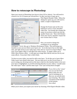
© Copyright 2026