
Publisher version
Downloaded from orbit.dtu.dk on: Jan 02, 2016 Towards Active Transducers Poulsen, Søren; Andersen, Michael A. E. Publication date: 2004 Document Version Publisher final version (usually the publisher pdf) Link to publication Citation (APA): Poulsen, S., & Andersen, M. A. E. (2004). Towards Active Transducers. Technical University of Denmark, Department of Electrical Engineering. General rights Copyright and moral rights for the publications made accessible in the public portal are retained by the authors and/or other copyright owners and it is a condition of accessing publications that users recognise and abide by the legal requirements associated with these rights. • Users may download and print one copy of any publication from the public portal for the purpose of private study or research. • You may not further distribute the material or use it for any profit-making activity or commercial gain • You may freely distribute the URL identifying the publication in the public portal ? If you believe that this document breaches copyright please contact us providing details, and we will remove access to the work immediately and investigate your claim. SØREN POULSEN Towards Active Transducers PhD thesis AUTOMATION Ørsted • DTU JULY 2004 Preface This Ph.D. thesis documents the research work performed in the ACT-ACtive Transducers research project at Ørsted·DTU, Technical University of Denmark in the period May 1. 2001 – June 30. 2004. The project has been financial founded by The Danish Energy Authority through the EFP2001 program, J.nr. 1273/01-006, and carried out in co-operation with Bang & Olufsen ICEpower A/S and Danish Sound Technology A/S. During the research project, I had the opportunity of a 3 month stay with the Audio Research Group, University of Waterloo, Canada, visiting professor John Vanderkooy. I would like to express my greatest appreciation to a number of people, who have personally played a special role for the results obtained in the project: • My adviser at Technical University of Denmark, professor Michael Andersen, for talking me into this project, and the very fruitful dialog and his support throughout the project • Professor John Vanderkooy, Audio Research Group, University of Waterloo, for his great inspiration and enthusiasm for everything within audio, and for his great friendliness • Assistant professor Nils Nielsen for our numerous discussions and for his great technical inspiration during the project • Ulrik Schmidt from Danish Sound Technology for the prototypes, he has made for the project • My family, who have had quite a bit fewer visits during this project • Last, but probably most important, I would like to express my deepest gratitude to my fiancé, Trine Bang, for her great forgiveness in busy periods, and for her support throughout this project, and above all, her belief in me. Lyngby July 5, 2004 Søren Poulsen Towards ACtive Transducers -Blank page- Abstract One of the trends within consumer audio systems is the requirement for surround sound systems, based on 5-7 or even more audio channels, resulting in the same number of power amplifier channels and loudspeakers for each system. Most systems on the market today are based on linear amplifiers techniques developed in the middle of last century, which is surprising when the last few decades' development within the audio source material, that is CD, DVD and SACD to mention the most popular, are taken into account. Audio performance of linear amplifiers has reached a level suitable for high quality audio reproduction many product generations ago, but the biggest disadvantages are still left untouched; power efficiency, size and cost. With today's technology, high efficient switch mode, or class D audio amplifiers based on pulse width modulation, PWM, are realizable. With the class D technology, consumer audio systems can benefit significantly from the highly increased power efficiency of class D amplifiers as well as their reduced size without need for bulky heat sinks, and also very important, low cost. The topic of this project is a total integration of switch mode audio amplifiers and loudspeakers into one single unit using the voice coil of the loudspeaker as output filter for the amplifier, with a perspective of highly reduced system power losses, system size and cost. Standard switch mode audio amplifiers and loudspeakers on the market are designed for use in traditional audio systems, and cannot without severe modifications be used for the integrated system without sacrifice of power efficiency. For this reason techniques for dedication of amplifier and loudspeaker for the specific purpose of the integration has been of major importance in this project. This thesis is a fundamental study of the loss mechanisms in loudspeakers and amplifiers and suggestions for optimizations are made to reduce the system power losses and cost without compromising the audio performance. Some of the results obtained in the project are redesign of and optimization of the parts in a loudspeaker, so the function of output filter for the amplifier can be obtained without significant power losses. Guidelines for dedication of speaker and amplifier to the integration process with significantly lower system power losses are also given. Furthermore, the work done in the project has resulted in new switch mode amplifier topologies, with very high audio performance realizable at a very low cost. Towards ACtive Transducers -Blank page- Resumé (abstract in Danish) Af de trends, der hersker indenfor konsumer audio systemer, er kravet om surround sound systemer med 5-7 eller flere lydkanaler, resulterende i samme antal effektforstærkerkanaler og højttalere. De fleste systemer er baseret på lineære forstærkerteknikker udviklet i midten af det sidste århundrede, hvilket kan synes bemærkelsesværdigt, når de sidste få årtiers udvikling indenfor audio lydkilder, f.eks. CD, DVD og SACD for at nævne de mest populære, tages i betragtning. Lydkvaliteten af lineære forstærkere har forlængst nået et niveau egnet for højkvalitets gengivelse af lyd, men de største ulemper ved den lineære forstærkerteknik er stadigvæk uberørt; energieffektivitet, størrelse og pris. Med dagens teknologi er højeffektive switch mode eller klasse D, forstærkere baseret på puls bredde modulation, PWM, realiserbare. Med klasse D teknikken kan konsumer audio systemer drage stor fordel af klasse D teknikkens væsentligt forøgede energieffektivitet samt kompakthed, da de ikke behøver store køleplader, og særdeles vigtigt, reduceret pris. Emnet for denne afhandling er en total integration af switch mode audio effektforstærkere og højttalere til en enkelt enhed, med brug af højttalerens svingspole som udgangsfilter for forstærkeren, med perspektiver som markant nedbragte system energitab, system størrelse og -pris. Standard switch mode audio forstærkere og højttalere på markedet er designede for brug i traditionelle audio systemer, og kan ikke uden væsentlige modifikationer bruges i det integrerede system uden at kompromittere energieffektiviteten, hvorfor teknikker til dedikering af forstærker og højttaler til dette formål har haft hovedprioritet i dette projekt. Denne afhandling er et grundlæggende studie af tabsmekanismerne i højttalere og forstærkere, og forslag til optimering er givet for at reducere det samlede systems effekttab og pris, uden at kompromittere dets audio ydelse. Nogle af de resultater, der er opnået i projektet, er redesign og optimering af delene i en højttaler, så den kan anvendes som udgangsfilter for forstærkeren, uden væsentlige effekttab, og retningslinier for dedikeringen af højttaler og forstærker til integreringen med en markant reduktion af systemets effekttab til følge. Endvidere har arbejdet i projektet resulteret i nye topologier til switch mode forstærkere med særdeles høj audio ydelse til en særdeles lav pris. Towards ACtive Transducers -Blank page- Table of Contents List of figures.................................................................................................................................5 List of tables................................................................................................................................12 List of abbreviations...................................................................................................................15 1 Introduction...............................................................................................................................17 2 Introducing ACT.......................................................................................................................19 3 Efficiency of switch mode amplifiers and loudspeakers.......................................................21 3.1 Loudspeaker efficiency........................................................................................................21 3.2 Switch mode amplifier efficiency........................................................................................24 3.3 Summary..............................................................................................................................25 4 Initial test setup.........................................................................................................................27 4.1 Subjective evaluation of acoustic output.............................................................................27 4.1.1 Measurement of acoustic output....................................................................................28 4.2 Initial test setup, power consumption...................................................................................28 4.3 Summary..............................................................................................................................31 5 Speaker motor system audio efficiency...................................................................................33 5.1 Magnetic field strength in the magnetic system air gap.......................................................34 5.2 Relative use of voice coil.....................................................................................................34 5.2.1 Voice coil fill factor.......................................................................................................36 5.2.2 Wire wound voice coils..................................................................................................40 5.2.3 Foil wound voice coils...................................................................................................40 5.3 Summary..............................................................................................................................43 6 Insulation material breakdown...............................................................................................45 6.1 Summary..............................................................................................................................47 7 Impedance of voice coil.............................................................................................................49 7.1 Proximity effect....................................................................................................................49 7.2 Voice coil capacitance..........................................................................................................52 7.3 Wire wound voice coils........................................................................................................52 7.3.1 Inserting a screen between the winding layers...............................................................55 7.3.2 Stray capacitances from winding to magnetic system....................................................57 -1- Towards ACtive Transducers 7.4 Foil wound voice coils.........................................................................................................58 7.4.1 Stray capacitances from winding to screen....................................................................59 7.5 Summary..............................................................................................................................59 8 Switch mode audio amplifiers..................................................................................................61 8.1 Basic PWM modulation schemes........................................................................................63 8.2 Power stage topologies for switch mode audio amplifiers...................................................71 8.2.1 Single ended power stage...............................................................................................71 8.2.1.1 Single ended power stage power supply pumping..............................................72 8.2.2 Full bridge power stage..................................................................................................75 8.3 Power stage switching losses...............................................................................................76 8.3.1 Switching losses, 2-level modulation.............................................................................78 8.3.2 Switching losses, 3-level modulation.............................................................................81 8.4 Summary..............................................................................................................................82 9 Modulator topologies for switch mode amplifiers.................................................................85 9.1 Standard PWM modulators..................................................................................................85 9.1.1 Standard PWM performance..........................................................................................87 9.2 Self oscillating modulators...................................................................................................87 9.3 Hysteresis modulators..........................................................................................................88 9.3.1 Current mode hysteresis modulators..............................................................................89 9.3.2 Voltage mode hysteresis controllers...............................................................................93 9.4 Subcategories of self oscillating modulators........................................................................95 9.4.1 Integrating time delay controlled modulators.................................................................95 9.4.2 Other types of self oscillating modulators......................................................................96 9.4.3 COM, Controlled Oscillation Modulator.......................................................................97 9.5 Modulator performance........................................................................................................99 9.6 Performance comparison of basic self oscillating modulators...........................................100 9.7 Carrier distortion................................................................................................................102 9.7.1 Designing modulators and additional feedback loops to maintain carrier cleanliness.105 9.8 GLIM, the Global Loop Integrating Modulator.................................................................107 9.8.1 GLIM loop function examples.....................................................................................110 -2- 9.9 Bandpass current mode modulators...................................................................................113 9.10 Constant switching frequency self oscillating hysteresis modulator................................117 9.11 Summary..........................................................................................................................119 10 Low cost implementations of self oscillating modulators..................................................121 10.1 Passive voltage mode modulators....................................................................................121 10.1.1 Passive hysteresis modulator......................................................................................122 10.1.2 Passive natural self oscillating modulator..................................................................126 10.1.3 Passive GLIM modulator with active control feedback loop.....................................127 10.2 Passive current mode modulators....................................................................................131 10.2.1 Passive BPCC modulator...........................................................................................131 10.2.2 Passive BPCC constant switching frequency hysteresis modulator...........................136 10.3 Examples of low cost modulators dedicated to ACT.......................................................140 10.3.1 Passive ACT hysteresis modulator.............................................................................141 10.3.2 Passive ACT BPCC modulator..................................................................................141 10.4 Summary..........................................................................................................................143 11 Synchronizing self oscillating modulators..........................................................................145 11.1 Summary..........................................................................................................................149 12 Prototype magnetic system...................................................................................................151 12.1 FEM simulations of prototype magnetic system..............................................................152 12.1.1 Simulated motor system efficiency............................................................................154 12.1.2 MLS impedance measurement system.......................................................................155 12.1.3 Prototype magnetic system measurements.................................................................156 12.2 Summary..........................................................................................................................159 13 ACT magnetic system power losses.....................................................................................161 13.1 Summary..........................................................................................................................165 14 ACT listening tests................................................................................................................167 15 Future work...........................................................................................................................171 16 Conclusion.............................................................................................................................173 17 References..............................................................................................................................177 -3- Towards ACtive Transducers Appendices Appendix A Power stage switching losses.................................................................................A1 Appendix B Current mode hysteresis modulator switching frequency.................................A4 Appendix C Prototype amplifiers..............................................................................................A5 C.1 Passive hysteresis prototype...............................................................................................A6 C.2 GLIM prototype................................................................................................................A10 C.3 BPCC self oscillating prototype.......................................................................................A14 C.4 Constant frequency hysteresis prototype..........................................................................A19 Appendix D Design of prototype magnetic system based on FEM simulations..................A22 D.1 Initial FEM simulations on modified magnetic systems..................................................A22 D.2 Prototype system FEM simulations..................................................................................A30 Appendix E CD ROM...............................................................................................................A33 Appendix F Publications..........................................................................................................A34 -4- List of figures Figure 3.1 1st order Bessel and Struve functions...........................................................................23 Figure 3.2 Normalized real (blue) and imaginary (red) part of radiation impedance....................23 Figure 3.3 Phase of radiation impedance (degrees).......................................................................23 Figure 4.1 ACT initial test setup....................................................................................................27 Figure 4.2 Left: With filter, Right: Without filter, SPL: 72dB......................................................28 Figure 4.3 Left: With filter, Right: Without filter, SPL: 93dB......................................................28 Figure 4.4 Impedance of the woofer used in the initial test setup, yellow: Magnitude of the impedance, blue: Phase shift of the impedance.............................................................................29 Figure 4.5 Voice coil stray capacitances between turns, windings and to surroundings (magnetic system)...........................................................................................................................................30 Figure 4.6 Calculated idle losses for the woofer, fs=300-575kHz.................................................30 Figure 5.1 Electrodynamic speaker................................................................................................33 Figure 5.2 Overhung and underhung voice coil............................................................................35 Figure 5.3 Wire wound voice coil, winding layout example 1......................................................37 Figure 5.4 Wire wound voice coil, winding layout example 2......................................................37 Figure 5.5 Wire wound voice coil, winding layout example 3......................................................38 Figure 5.6 Wire wound voice coil, winding layout example 4......................................................38 Figure 5.7 Wire wound voice coil, winding layout example 5......................................................39 Figure 5.8 Fill factors for winding layout example 1, 2, 3, 5 vs. insulation-conductor thickness ratio................................................................................................................................................39 Figure 5.9 Wire wound voice coil, equivalent model....................................................................40 Figure 5.10 Foil wound voice coil, equivalent model...................................................................41 Figure 5.11 High frequency current density of a foil winding.......................................................41 Figure 5.12 LF eddy currents generated in a foil...........................................................................41 Figure 5.13 Slitting a foil winding to reduce low frequency eddy currents in the foil..................42 Figure 5.14 Voice coil with parallel or rectangular winding thread..............................................42 Figure 5.15 Prototype foil wound voice coils................................................................................43 Figure 6.1 Layer to layer voltage, 2-layer winding........................................................................45 Figure 6.2 Single layer voice coil with return wire........................................................................46 Figure 6.3 Layer to layer voltage, 4-layer winding........................................................................46 -5- Towards ACtive Transducers Figure 7.1 Wire wound voice coil, equivalent model....................................................................49 Figure 7.2 Proximity effect, conductor thickness normalized with penetration depth, p=1..10....51 Figure 7.3 Proximity effect, conductor thickness normalized with penetration depth, p=30..50. .51 Figure 7.4 Parasitic capacitances of voice coil..............................................................................52 Figure 7.5 Per length wire to wire capacitance..............................................................................52 Figure 7.6 Wire wound voice coil..................................................................................................53 Figure 7.7 Voltage between layers for a p-layer coil.....................................................................53 Figure 7.8 Wire wound voice coil, equivalent model....................................................................54 Figure 7.9 2-layer voice coil with a grounded screen inserted between the winding layers..........56 Figure 7.10 Voltage between coil and magnetic system for a p-layer coil....................................57 Figure 8.1 Class B output stage, normalized transistor voltage (VT), output current (IT), power loss (PT), output power (Po) vs. time in angular frequency, one quarter input period..................61 Figure 8.2 Class A (PTA) and B (PTB) output stage, power loss, output power (Po) vs. modulation index M.......................................................................................................................61 Figure 8.3 Class A (ηA) and Class B (ηB) output stage efficiency for a sinusoidal signal with modulation index M.......................................................................................................................62 Figure 8.4 Class D full ridge output stage.....................................................................................62 Figure 8.5 2-level NADS modulation waveforms.........................................................................63 Figure 8.6 2-level NADD modulation waveforms.........................................................................64 Figure 8.7 3-level NBDS modulation waveforms.........................................................................65 Figure 8.8 3-level NBDD modulation waveforms.........................................................................66 Figure 8.9 FFT 2-level NADS, M=0.01, M= 1..............................................................................67 Figure 8.10 FFT 2-level NADD, M=0.01, M= 1...........................................................................67 Figure 8.11 FFT 2-level NBDS, M=0.01, M=1.............................................................................68 Figure 8.12 FFT 2-level NBDD, M=0.01, M=1............................................................................68 Figure 8.13 FFT 2-level NBDS, common mode, M=0.01, M=1...................................................69 Figure 8.14 FFT 2-level NBDD, common mode, M=0.01, M=1..................................................69 Figure 8.15 PSU and single ended output stage.............................................................................72 Figure 8.16 Single ended power stage, power flow.......................................................................72 Figure 8.17 Unidirectional PSU and single ended power amplifier..............................................72 Figure 8.18 Supply pumping, sourcing energy..............................................................................73 -6- Figure 8.19 Supply pumping, charging energy..............................................................................73 Figure 8.20 Supply-pumping, minimum decoupling capacitor.....................................................75 Figure 8.21 PSU and full bridge output stage................................................................................75 Figure 8.22 Full bridge power stage, power flow..........................................................................76 Figure 8.23 MOSFET equivalent schematic..................................................................................77 Figure 8.24 Power stage losses vs. output power, half bridge (solid) and full bridge (dotted), US = 5 (red), 10 (blue), 20 (green), 40V (magenta).............................................................................80 Figure 8.25 Power stage losses vs. output power, half bridge (solid) and full bridge (dotted), tdead = 0 (red), 20ns (blue), 40ns (green), 60ns (magenta)...........................................................81 Figure 8.26 Power stage losses vs. supply voltage, full bridge, 3-level modulation.....................82 Figure 9.1 Standard PWM.............................................................................................................85 Figure 9.2 Standard PWM, Carrier and reference (above), PWM and filtered output (below), M=1................................................................................................................................................85 Figure 9.3 Standard PWM.............................................................................................................86 Figure 9.4 Standard PWM, summed carrier and reference (above), PWM and filtered output (below), M=1.................................................................................................................................86 Figure 9.5 Example carrier generator............................................................................................87 Figure 9.6 Example carrier generator block diagram.....................................................................87 Figure 9.7 Self oscillating modulator block diagram.....................................................................88 Figure 9.8 Current mode hysteresis modulator..............................................................................89 Figure 9.9 Current mode hysteresis modulator, inductor current and carrier waveform, M=0.5. .89 Figure 9.10 Switching frequency vs. M, normalized with idle switching frequency.....................90 Figure 9.11 Realization of hysteresis window from the power supply..........................................91 Figure 9.12 Current mode hysteresis modulator, output voltage, inductor current and carrier waveform, M=0.8..........................................................................................................................91 Figure 9.13 Example of voltage gain, load = 1Ω (green), 2Ω (red), 4Ω (blue), 8Ω (magenta), 100Ω (turquoise)............................................................................................................................92 Figure 9.14 Voltage mode hysteresis modulator [EL01]...............................................................93 Figure 9.15 Voltage mode hysteresis modulator, power stage output voltage, carrier waveform and reference, M=0.5.....................................................................................................................93 Figure 9.16 Voltage mode hysteresis modulator, power stage output voltage, carrier waveform and reference, M=0.8.....................................................................................................................94 -7- Towards ACtive Transducers Figure 9.17 Self oscillating modulator with propagation delay control of switching frequency, power stage output voltage, carrier waveform and reference, M=0.5............................................95 Figure 9.18 Self oscillating modulator [Ge01]..............................................................................96 Figure 9.19 Self oscillating modulator illustrated in Figure 9.18, power stage output voltage, carrier waveform and reference, M=0.5.........................................................................................97 Figure 9.20 Block diagram of COM modulator [Ni02].................................................................97 Figure 9.21 COM modulator, power stage output voltage, carrier waveform and reference, M=0.5 .......................................................................................................................................................98 Figure 9.22 COM modulator, power stage output voltage, carrier waveform and reference, M=0.8 .......................................................................................................................................................99 Figure 9.23 Voltage mode hysteresis (blue) and COM modulator (red), open loop gain (above) and phase (below) functions........................................................................................................101 Figure 9.24 Voltage mode hysteresis (blue) and COM modulator (red), FFT, fin=5kHz, M=0.8.... 101 Figure 9.25 Voltage mode hysteresis (blue) and COM modulator (red), FFT, fin=5kHz, M=0.8.... 102 Figure 9.26 Voltage mode hysteresis (blue) and COM modulator (red), FFT, fin=1kHz, M=0.4, PS: ±40% (10kHz sine)................................................................................................................102 Figure 9.27 Control output, "Perfect" and resulting carrier.........................................................103 Figure 9.28 Carrier distortion, carrier waveform (solid) and modulator gain (dotted) for “perfect” (red) and resulting (blue) carrier..................................................................................................104 Figure 9.29 FFT spectrum for modulation with "perfect" (red) and resulting (blue) carrier, M=0.8 .....................................................................................................................................................105 Figure 9.30 Open loop definitions of a multi loop system...........................................................106 Figure 9.31 Modulator and control loop example 1....................................................................106 Figure 9.32 Example 1, modulator and control loop functions...................................................106 Figure 9.33 Modulator and control loop example 2....................................................................107 Figure 9.34 Example 2, modulator and control loop functions...................................................107 Figure 9.35 GLIM principal diagram...........................................................................................108 Figure 9.36 GLIM modulator loop, principal diagram................................................................109 Figure 9.37 GLIM realization example 1.....................................................................................109 Figure 9.38 GLIM realization example 2.....................................................................................109 Figure 9.39 GLIM realization example 1 open loop functions, load= 1Ω, 2Ω, 4Ω, 8Ω, 100Ω, open..............................................................................................................................................111 -8- Figure 9.40 GLIM realization example 2 open loop functions, load= 1Ω, 2Ω, 4Ω, 8Ω, 100Ω, open..............................................................................................................................................111 Figure 9.41 GLIM realization example 1 closed loop functions, load= 1Ω, 2Ω, 4Ω, 8Ω, 100Ω, open..............................................................................................................................................112 Figure 9.42 GLIM realization example 2 closed loop functions, load= 1Ω, 2Ω, 4Ω, 8Ω, 100Ω, open..............................................................................................................................................112 Figure 9.43 GLIM realization example 1 (above) and 2 (below) sensitivity functions, load= 1Ω, 2Ω, 4Ω, 8Ω, 100Ω, open..............................................................................................................113 Figure 9.44 BPCC self oscillating modulator concept.................................................................114 Figure 9.45 BPCC open loop functions,load= (gain from above, phase from bellow) 1Ω, 2Ω, 4Ω. 8Ω, 100Ω, open............................................................................................................................115 Figure 9.46 BPCM closed loop functions, load= (gain and phase from bellow) 1Ω, 2Ω, 4Ω. 8Ω, 100Ω, open...................................................................................................................................116 Figure 9.47 BPCM sensitivity loop functions, load = 1Ω, 2Ω, 4Ω. 8Ω, 100Ω, open..................116 Figure 9.48 Hysteresis modulator with variable hysteresis window [Ve01]...............................117 Figure 9.49 Hysteresis modulator with variable gain amplifier window.....................................117 Figure 9.50 Proposed constant switching frequency current mode modulator............................118 Figure 10.1 Passive linear hysteresis modulator..........................................................................122 Figure 10.2 Passive linear hysteresis modulator prototype, effective open loop functions, load = 1Ω, 2Ω, 4Ω. 8Ω, 100Ω, open.......................................................................................................123 Figure 10.3 Passive linear hysteresis modulator prototype, closed loop functions, load = 1Ω, 2Ω, 4Ω. 8Ω, 100Ω, open.....................................................................................................................124 Figure 10.4 Passive linear hysteresis modulator prototype sensitivity functions, load = 1Ω, 2Ω, 4Ω. 8Ω, 100Ω, open.....................................................................................................................124 Figure 10.5 Passive linear hysteresis modulator prototype..........................................................124 Figure 10.6 Passive linear hysteresis modulator prototype transient simulation, Output voltage (above), carrier (below)................................................................................................................125 Figure 10.7 Passive hysteresis prototype carriers, idle, M=0.5....................................................125 Figure 10.8 Passive hysteresis prototype THD+n vs. power, load=4Ω, f=100Hz (green), 1kHz (blue), 6.67kHz (red), BW=20kHz..............................................................................................126 Figure 10.9 UCD passive self oscillating modulator [Pu02].......................................................126 Figure 10.10 GLIM passive modulator loop................................................................................127 Figure 10.11 Shaping control feedback loop for passive GLIM modulator loop example..........127 Figure 10.12 Prototype GLIM implementation with passive modulator loop and active control loops.............................................................................................................................................128 -9- Towards ACtive Transducers Figure 10.13 GLIM Prototype simulation, open loop functions, load = 1Ω, 2Ω, 4Ω. 8Ω, 100Ω, open..............................................................................................................................................129 Figure 10.14 GLIM Prototype simulation, closed loop functions, load = 1Ω, 2Ω, 4Ω. 8Ω, 100Ω, open..............................................................................................................................................129 Figure 10.15 GLIM Prototype simulation, sensitivity functions, load = 1Ω, 2Ω, 4Ω. 8Ω, 100Ω, open..............................................................................................................................................129 Figure 10.16 GLIM Prototype amplifier......................................................................................130 Figure 10.17 GLIM Prototype transient simulation, Output voltage (above), carrier (red) and feedback block outputs (blue, magenta) (below).........................................................................130 Figure 10.18 GLIM Prototype measurements, carrier and output voltage, idle, M=0.5 load = 4Ω... 130 Figure 10.19 GLIM prototype THD+n vs. power, load=4Ω, f=100Hz (green), 1kHz (blue), 6.67kHz (red), BW=20kHz..........................................................................................................131 Figure 10.20 Low cost BPCC self oscillating modulator implementation..................................131 Figure 10.21 Current estimation with a dual inductor secondary winding and low cost opamp [Ri02]...........................................................................................................................................132 Figure 10.22 Low cost BPCC self oscillating modulator implementation..................................133 Figure 10.23 BPCC prototype simulation sensitivity functions, load = 1Ω, 2Ω, 4Ω. 8Ω, 100Ω, open..............................................................................................................................................134 Figure 10.24 BPCC prototype simulation sensitivity functions, load = 1Ω, 2Ω, 4Ω. 8Ω, 100Ω, open..............................................................................................................................................134 Figure 10.25 BPCC prototype simulation sensitivity functions, load = 1Ω, 2Ω, 4Ω. 8Ω, 100Ω, open..............................................................................................................................................134 Figure 10.26 BPCC self oscillating amplifier prototype..............................................................135 Figure 10.27 BPCC prototype simulation, output voltage (above), carrier (red) and control feedback outputs (blue, magenta) (below), fin=8kHz, M=0.8, load=4Ω.....................................135 Figure 10.28 BPCC prototype carrier measurements, idle, M=0.5..............................................135 Figure 10.29 BPCC self oscillating prototype THD+n vs. power, load=4Ω, f=100Hz (green), 1kHz (blue), 6.67kHz (red), BW=20kHz....................................................................................136 Figure 10.30 Low cost BPCC constant switching frequency hysteresis modulator implementation .....................................................................................................................................................136 Figure 10.31 BPCC constant switching frequency prototype......................................................138 Figure 10.32 Simulated BPCC constant switching frequency example carrier signals, M=0, 0.8.... 138 Figure 10.33 Prototype BPCC constant switching frequency example carrier signals, M=0, 0.8..... 138 -10- Figure 10.34 Simulated BPCC constant switching frequency example, FFT of output, fin=1kHz, M=0.8...........................................................................................................................................139 Figure 10.35 Prototype BPCC constant switching frequency example, FFT of output, fin=1kHz, M=0.8...........................................................................................................................................139 Figure 10.36 Prototype BPCC constant switching frequency example, FFT of output, fin=100Hz, 10Hz, M=0.8................................................................................................................................139 Figure 10.37 Normalized switching frequency vs. DC modulation, prototype (blue) and standard (red) hysteresis modulator............................................................................................................140 Figure 10.38 Modifying feedback for filterless applications.......................................................140 Figure 10.39 Passive ACT hysteresis modulator.........................................................................141 Figure 10.40 Passive ACT BPCC modulator..............................................................................141 Figure 10.41 Using the voice coil as coupled inductor for BPCC modulator.............................142 Figure 10.42 Passive ACT BPCC modulator with standard voice coil.......................................142 Figure 10.43 Measuring back EMF by resistive network............................................................142 Figure 10.44 Measuring back EMF by BPCC inductor...............................................................143 Figure 11.1 Synchronization of two self oscillating modulators.................................................145 Figure 11.2 Modulator synchronization using output filter capacitance......................................146 Figure 11.3 Modulator synchronization using summed carriers (SCOM) [In01], [Ni05]...........146 Figure 11.4 Modulator synchronization using summed hysteresis windows [Po06], [Po11]......147 Figure 11.5 SCOM [Ni05] waveforms, synchronization current (above), reference and carriers (below).........................................................................................................................................148 Figure 11.6 Synchronized hysteresis windows waveforms, synchronization current (above), one hysteresis window (middle), reference and carriers (below).......................................................148 Figure 12.1 Standard magnetic system, voice coil (black), magnet (gray), iron parts (light gray).... 151 Figure 12.2 Modified magnetic system 1 example, voice coil (black), magnet (gray), iron parts (light gray), replaced parts (dark gray).........................................................................................151 Figure 12.3 Modified magnetic system 2 example, voice coil (black), magnet (gray), iron parts (light gray), replaced parts (dark gray).........................................................................................151 Figure 12.4 Color scale for the FEM simulation shade plots......................................................152 Figure 12.5 Prototype 42mm system 1, -26 powder iron material...............................................153 Figure 12.6 Prototype 42mm system 2, -26 powder iron material...............................................153 Figure 12.7 Prototype 50mm magnetic system, FEM simulation................................................153 -11- Towards ACtive Transducers Figure 12.8 Standard 50mm magnetic system, FEM simulation.................................................154 Figure 12.9 MLS impedance measurement system.....................................................................156 Figure 12.10 MLS impedance measurement setup......................................................................156 Figure 12.11 Short coil impedance measurement, standard system, coil position: Above (blue), in (green), below (red) air gap..........................................................................................................157 Figure 12.12 Short coil impedance measurement, prototype system, coil position: Above (blue), in (green), below (red) air gap.....................................................................................................158 Figure 12.13 Standard coil impedance measurement, standard (green) and prototype (blue) system..........................................................................................................................................159 Figure 12.14 Standard coil phase measurement, standard (green) and prototype (blue) system. 159 Figure 13.1 Blocked cone impedance, standard (green) and prototype (blue) magnetic system. 161 Figure 13.2 Power losses vs. fs, NADD 2-level modulation, standard system, M=0 (blue), 0.25 (green), 0.5 (red) , 0.75 (magenta), 1 (orange).............................................................................162 Figure 13.3 Power losses vs. fs, NADD 2-level modulation, prototype system, M=0 (blue), 0.25 (green), 0.5 (red) , 0.75 (magenta), 1 (orange).............................................................................163 Figure 13.4 Power losses vs. fs, NBDD 3-level modulation, standard system, M=0.25 (green), 0.5 (red) , 0.75 (magenta), 1 (orange)..........................................................................................164 Figure 13.5Power losses vs. fs, NBDD 3-level modulation, prototype system, M=0.25 (green), 0.5 (red) , 0.75 (magenta), 1 (orange)..........................................................................................164 Figure 14.1 Equipment setup for recording of ACT amplifier electrical output.........................167 Figure 14.2 ACT test amplifier, voice coil and magnetic system from a 10” woofer................168 Figure 14.3 Equipment setup for evaluation of recordings of ACT amplifier electrical output..168 List of tables Table 3.1 ICE250A amplifier module, power specifications [IC01].............................................24 Table 3.2 ICE250A output filter core (Micrometals T94-2) parameters.......................................25 Table 4.1 Initial test setup, idle power losses................................................................................29 Table 8.1 Natural sampling PWM modulation schemes...............................................................63 Table 8.2 Fourier series used for NADS, NADD, NBDS and NBDD modulation.......................71 Table 8.3 Switching loss parameters.............................................................................................77 Table 9.1 Voltage mode hysteresis and COM modulator example simulation parameters.........100 Table 9.2 Characteristic parameters for GLIM example 1 and 2.................................................110 Table 9.3 GLIM simulation example parameters........................................................................110 -12- Table 9.4 BPCC self oscillating modulator example parameters................................................115 Table 10.1 Passive hysteresis modulator prototype parameters...................................................123 Table 10.2 GLIM prototype parameters.......................................................................................128 Table 10.3 BPCC self oscillating modulator prototype parameters.............................................133 Table 10.4 BPCC self oscillating modulator prototype parameters.............................................137 Table 12.1 Voice coil data for FEM simulations.........................................................................154 Table 12.2 FEM test results, 42mm systems...............................................................................155 Table 13.1 Parameters used for magnetic system power loss calculations..................................162 Table 14.1 Listening test results..................................................................................................169 -13- Towards ACtive Transducers -Blank page- -14- List of abbreviations ACT ACtive Transducers BPCC Band Pass Current Control CFB Control FeedBack CFW Control ForWard FEM Finite Element Method FFT Fast Fourier Transformation MLS Maximum Length Signal MFB Modulator FeedBack MFW Modulator ForWard NADD Natural sampling, AD, Double sided modulation NADS Natural sampling, AD, Single sided modulation NBDD Natural sampling, BD, Double sided modulation NBDS Natural sampling, BD, Single sided modulation PWM Pulse Width Modulation PSRR Power Supply Rejection Ratio SS Statistical Significance THD Total Harmonic Distortion -15- Towards ACtive Transducers -Blank page- -16- Introduction 1 Introduction Development of audio power amplifiers has gained significantly through the last two decades with the development of audio quality switch mode, or class D, power amplifiers. Apart from class D type power amplifiers, development of audio power amplifiers has been concentrated on minor performance improvement of linear amplifiers, but using the same overall power circuitry since transistor based power stages from the middle of last century. Even though performance of linear amplifiers have reached a performance level required for high performance audio reproduction several decades ago, the basic concept of linear power amplifiers is strongly burdened by poor power efficiency, high cost, and large physical size. With the increasing demand for more audio channels in today's popular multi channel surround sound systems, audio design based on linear amplifiers suffers from fast growing bulk, weight and cost, but a still larger focus on the total system power consumption and thereby running cost, influences the manufactures' which for smaller, cheaper, and certainly also more power efficient amplifier topologies. Development of loudspeakers for audio reproduction systems has as in the case of audio power amplifiers, also primarily relied on minor improvements of the basic concept of electrodynamic loudspeakers developed in the beginning of last century. Other types of loudspeakers than the electrodynamic loudspeaker are available on the market, where especially electrostatic [Ra01] loudspeakers have a strong position in the high end segment of the market. New types of speakers such as NXT [Az01] are showing up, but even though it uses a distributed resonance mode for radiating the acoustical output, the motor system itself is principally identical to the motor system of an electrodynamic loudspeaker. The trend within consumer audio electronics of today has changed from two way stereo which dominated the market up to about a decade ago, into multichannel surround sound systems with 5 or more like 7 or 9 channels. The need for still more audio channels favors active loudspeaker systems over traditional passive systems. In an active loudspeaker system, the power amplifier is placed inside the loudspeaker box, which gives the manufacturer the opportunity of dedicating amplifier and speaker to each other, as well as use of active crossovers for the loudspeaker if separate power amplifiers are used for each speaker driver. Active loudspeakers with active crossovers achieve certain benefits over separate amplifiers and passive loudspeakers. First of all, the crossover can be realized with electronics only handling a line signal level, which gives a higher freedom of achievable crossover filter approximation functions and equalizing. Second, features such as motional feedback can be built into the system to give an active extension to the lower end of the frequency range with flat output response. The actual success of offering multichannel systems is strongly related to cost and size. With class D amplifiers, it has been possible to build power amplifiers with a cost, size and efficiency that is far superior to linear power amplifiers. Furthermore both audio quality and output power levels have proved to be at least on par with the better linear amplifier designs, but at a significantly lower cost, size, weight and significantly higher power efficiency. In a country like Denmark, DEFU, Research Institute for Danish Electric Utilities, has estimated the annual electrical power consumption of consumer electronics to be 739 GWh/year (exclusive standby consumption). Out of this quantity, audio power amplifiers are estimated to -17- Towards ACtive Transducers use 145GWh/year [DE01]. Since almost all power amplifiers in practical use are based on linear topologies, this consumption could be greatly reduced if all amplifiers were changed to newer types class D amplifiers. If all amplifiers in Denmark were changed to amplifiers based om switch mode principles such as the ICEpower amplifier modules, the annual electric energy consumption could be reduced to an estimated 33GWh/year. The goal for this Ph.D. project has been to investigate the possibility of a total integration of electrodynamic loudspeakers and switch mode audio power amplifiers with a strong emphasis on increased power efficiency without compromising audio performance or cost. By integrating the two, the magnetic structure of the loudspeaker can be used as heatsink for the amplifier, as well and the ideally true inductive behaviour of the speaker can be used as output filter for the amplifier, thereby acting as a part of the amplifier, yielding a true integrated system. The benefits of this integration is a potentially reduced system cost, and by dedicating the devices to the integrated system, an increase in power efficiency is expected. The overall goal for this Ph.D. project is an increase of power efficiency of today's state of the art combination of electrodynamic loudspeakers and ICEpower technology based amplifiers. The specific goal is a reduction of the estimated 33GWh/year to 5GWh/year, by an increase in power efficiency of a factor of 4 at high output levels and a reduction of the system idle losses by a factor of 2 compared to today's ICEpower technology. -18- Introducing ACT 2 Introducing ACT The key concept in ACT, ACtive Transducers is integrating switch mode amplifiers and electrodynamic loudspeakers into one single unit, using the voice coil of the loudspeaker as output filter for the amplifier. By the integration, the traditional interface, voltage control and 48Ω impedance, between amplifier and loudspeaker can be broken down, giving a new degree of freedom of designing dedicated amplifiers and speakers for the integration. Integration of amplifier and speaker has been proposed in [Bi01]. This patent proposes integration of a linear amplifier and an electrodynamic loudspeaker, using the magnetic structure of the loudspeaker as heatsink for the amplifier. Using the voice coil of the loudspeaker as output filter for the amplifier has been proposed in [TI01], however, the application note as well as the filterless switch mode amplifiers made by Texas Instruments [TI02] are targeting only low power solutions and use of standard loudspeakers. Integration of switch mode audio amplifiers and electrodynamic loudspeakers using the voice coil of the loudspeaker as output filter for the amplifier is later proposed in [Ni03]. Even though the concept of integrating switch mode amplifiers and electrodynamic loudspeakers does not differ significantly from prior art, the perspectives for the integration are interesting: • Power efficiency can potentially be increased over prior art by dedication of amplifier and speaker for the integration. • Cost of the combined amplifier and speaker can be reduced due to savings on heatsinks and amplifier output filter, and by the increased efficiency, decreasing price for equal maximum acoustic output. • Optional extra options such as motional feedback and overload protection can easily be implemented. -19- Towards ACtive Transducers -Blank page- -20- Efficiency of switch mode amplifiers and loudspeakers 3 Efficiency of switch mode amplifiers and loudspeakers Efficiency of an audio system can be measured in a number of ways. Often the idle consumption of an amplifier is given in the datasheet and sometimes the power consumption at maximum output power as well. For a loudspeaker, the efficiency is often given as the sound pressure level, SPL, at 1m distance when the loudspeaker has applied a signal at 2.83VRMS amplitude, which equals a power of 1W in a 8Ω load. However, the electrical impedance of a loudspeaker is rarely 8Ω, and the electrical impedance of a typical loudspeaker differs significantly from a resistive load, making the impedance strongly dependent on frequency. Looking at the system efficiency, the applications in which the system is used should be taken into account. The target for this project is consumer audio systems, hence the evaluation should be for use in such systems. General use of consumer audio equipment includes everything from idle to background music, more realistic listening levels, and party levels, but the average use of the equipment is for low level output, giving a poor utilization of the power capability of the amplifier and speaker. Furthermore, the average signal level compared to the peak levels, the crest factor, is high for all music, meaning that high output levels are only required for very short time intervals, even if the volume of the system is at maximum. The frequency distribution of the power levels in music is an important design factor as well as the crest factor. At high frequencies, the average power level is vanishing small, since it mostly consists of short transients. The dominant frequency range for the power distribution is at low frequencies, thus a valid estimate for music could be pink noise, which is lowpass filtered white noise [Hø01]. Optimization of the power efficiency of an audio system should result in lowest power consumption, averaged over the entire product life, and attention should be paid to optimize the system for its average use, that is for very low output powers and idle. Since the frequency distribution of the power levels of music can be considered a lowpass function with a low pole frequency, the aim of this project will be at woofer applications for low frequency sound reproduction. 3.1 Loudspeaker efficiency The efficiency for a loudspeaker is strongly dependent on the speaker parameters as well as the operating frequency range. An electrodynamic speaker working in its mass controlled range, where it achieves a flat output response, has an acoustic output power and efficiency given by [Ra01]: 1 P a= c S⋅Bl⋅U mmmm , r R s 2 , f 0≪ f U2 P in≈ Rs P 1 S⋅Bl speaker = a ≈ P in R s⋅ c mmmm , r -21- (3.1) 2 , f 0≪ f Towards ACtive Transducers where: U speaker terminal voltage Ω radiation angle = 2π for the speaker mounted in an infinite baffle = 4π for the speaker mounted in a small box ρ air density c velocity of sound S diaphragm area Bl loudspeaker force factor mm loudspeaker moving mass mm,r equivalent moving air mass f0 mechanical resonance frequency Rs DC resistance of the voice coil The acoustic output of the speaker is a bandpass response, with a power output increasing by 4th order for frequencies below f0. At higher frequencies, the piston range is limited by the frequency where the length of a half wavelength of the audio output equals the diaphragm diameter. Above this frequency the output power response ideally falls by 2nd order, and is largely influenced by resonances of the diaphragm. Typical efficiency of an electrodynamic loudspeaker is on the order of 1-2% due to a close to true imaginary mechanical to acoustic coupling between the loudspeaker diaphragm and the air at low frequencies. The mechanical to acoustic radiation impedance is given by [Ra02], [Ra01]: Z m , r = c a 2 12 J 1 2 H 1 2⋅ka 2⋅ka j 2⋅ka 2⋅ka (3.2) where ρ is air density, c velocity of sound, k = ω/c, a=diaphragm radius, J1 the 1st order Bessel function and H1 the 1st order Struve function given by [Pi01]: H 1 z = 2z 2 ∫ sin z cos ⋅sin 2 0 -22- (3.3) Efficiency of switch mode amplifiers and loudspeakers Figure 3.1 1st order Bessel and Struve functions Figure 3.2 Normalized real (blue) and imaginary (red) part of radiation impedance Figure 3.3 Phase of radiation impedance (degrees) It is seen that the radiation impedance has a large imaginary part for frequencies up to well above ka=1 which defines the upper range of the piston range of the loudspeaker. ka=1 equals the frequency, where the diameter of the speaker diaphragm is half a wavelength of an acoustic signal with this frequency. -23- Towards ACtive Transducers From (3.1) it is seen that the efficiency of the speaker can be improved by: • Increasing the diaphragm area • Increasing the force factor [Va02], [Va03] • Decreasing the moving mass • Decreasing the voice coil DC resistance • Increasing the real part of the mechanical to acoustic radiation impedance Increasing the efficiency by modifying diaphragm will compromise the moving mass of the system and is not necessarily an improvement. Increasing the force factor can be obtained by using a stronger magnet or more winding turns on the voice coil, increasing system cost and power losses respectively. However one possibility is modifying the DC resistance of the voice coil which will be addressed later in this report. Increasing the real part of the radiation impedance can be obtained with various types of horn speakers [Le01], but due to the large wavelengths at low frequencies, these systems becomes physically large and will not be suited to consumer applications. For this reason they will not be addressed further in this report. 3.2 Switch mode amplifier efficiency The power efficiency of a switch mode amplifier is strongly dependent on a number of design parameters. The ICE250A from ICEpower [IC01] is taken as an illustration of today's state of the art switch mode amplifiers, as this amplifier module have been used as reference in the ACT project. Power specifications for the ICE250A switch mode amplifier module: min Power supply 48V (fs = 450kHz) Power stage 100W/8Ω efficiency, 30mA, 1.44W η, typ 40mA, 1.92W max 50mA, 2.4W 93.00% Table 3.1 ICE250A amplifier module, power specifications [IC01] The ICE250A amplifier module has an output filter with an inductor wound on a T94-2 iron powder core from Micrometals. The idle core losses of the inductor are caused by the output filter ripple current. The magnetic peak to peak flux variation, ∆B, of the output filter core of the ICE250 amplifier is given by [Mi01]: 8 V 10 B= S 2AN f s where -24- [Gauss] (3.4) Efficiency of switch mode amplifiers and loudspeakers Symbol ICE250 A Core cross section area [cm2] N Number of winding turns fs Switching frequency VS 0.362cm2 52 450kHz Supply voltage 48V Table 3.2 ICE250A output filter core (Micrometals T94-2) parameters B=283.33Gauss=28.33 mT P core [ wW / cm ]= 3 (3.5) f 2 2 d f B a b c B 3 B 2.3 B1.65 (3.6) with B in Gauss. For the Micrometals T94 core with -2 material, the following parameters are given: V core =2.16 cm 3 a=4⋅10 9 b=3⋅10 8 c=2.7⋅10 6 15 d =8⋅10 The idle core power loss of the ICE250A amplifier is 1.16W using a 48V power supply, which is a relatively large value, about 50% of idle power consumption of the entire power stage and output filter. 3.3 Summary Designing amplifiers and loudspeakers for consumer applications to reach a higher power efficiency should be done with the consumer's use of audio systems in mind. Typically use of consumer audio systems is generally at low output levels, thus idle consumption and efficiency at low output levels should be weighted significantly higher than efficiency at full output level. Efficiency at high output power levels is not an important design parameter, since even if the audio system is used at maximum output level, the high crest factor, the ratio between peak and average values of music, makes low power efficiency much more important. However, the thermal design of the system should still allow high continuous output levels without thermal problems. The frequency distribution of the power level in music is comparable to pink noise, why improvement of the efficiency at low frequencies will have far the largest impact for overall system efficiency, thus the focus will be on woofers. Efficiency of loudspeakers is in the range of 1-2%, and leaves room for improving the electrical impedance. Efficiency for an ICEpower -25- Towards ACtive Transducers amplifier is typically 93% at 100W/8Ω, and with power stage and output filter idle consumption between 1.44 and 2.4W. The idle core loss of the output filter inductor is 1.16W, which means that the idle consumption and low output power efficiency of the combined ACT amplifier and loudspeaker can be improved by approximately a factor of 2 if this core loss is not moved to the loudspeaker. -26- Initial test setup 4 Initial test setup A test setup for an initial test of direct switching of a loudspeaker was built at an early stage of the project. The setup was not intended for high precision measurements of either acoustic output or electrical behavior, but only to illustrate the initial problems of the integration of a switch mode amplifier and an electrodynamic loudspeaker, using the voice coil of the speaker as output filter for the amplifier. Furthermore the setup would be able to envestigate possible audible unwanted effects of the combination. Figure 4.1 ACT initial test setup The test setup was as following: Sub woofer: • Scan-Speak 10” woofer in a vented box • Modified by cutting a cross through the pole piece to reduce eddy current losses Sub amplifier: • ICE250A amplifier using 2-level modulation • Modified by disconnecting the outer control loop • Idle switching frequency adjusted to 500kHz • A relay connected across the output filter, making possible filtered and unfiltered output signals Rest of system: • PSU, power supply (for amplifier output stages): 50V • Active crossover, 150Hz 4th order Butterworth • ICE250A amplifier for upper frequencies • Rogers LS3/5A speakers for upper frequency range 4.1 Subjective evaluation of acoustic output Initially the acoustic output was evaluated in subjective listening tests. The initially tests -27- Towards ACtive Transducers showed no change in tonal balance or audible distortion with the amplifier driving the woofer directly compared to the filtered output. One listener could, however, detect a slight negative difference in pulse response in the bass region when using the output filter. Since the output filter inductor has a conducting resistance, raising the output impedance of the amplifier, this could be an explanation of the possible difference. However, even it was favoring the direct switching, it was an insignificant change in output response, and due to the fact that it was not based on any statistic verification, the indications of the initial test was that direct switching of the loudspeaker is possible without distorting the output. 4.1.1 Measurement of acoustic output The acoustic output was also measured in an non reverberation chamber using 100Hz test signals with SPL of 72 and 93 dB respectively. These measurements are shown in Figure 4.2 and 4.3. Figure 4.2 Left: With filter, Right: Without filter, SPL: 72dB Figure 4.3 Left: With filter, Right: Without filter, SPL: 93dB The measurements in Figure 4.2 and 4.3 show no measurable difference in the acoustic output of the woofer when using either filtered or unfiltered output of the amplifier. 4.2 Initial test setup, power consumption The idle input current to the speaker was measured using a high frequency spectrum analyzer. The total power applied to the amplifier and speaker was measured with and without output filter -28- Initial test setup for the amplifier: With output filter Without output filter Pspeaker, idle ≈ 0W Pspeaker, idle ≈ 2.8W Pamplifier ≈ 1.6W Pamplifier ≈ 1.65W Table 4.1 Initial test setup, idle power losses Ideally power losses in the speaker should be small in both the filtered and unfiltered case, since an ideal speaker impedance should be an ideal inductor with a relatively small DC resistance (blocked cone model). However, the unfiltered power consumption more than indicates clearly that the real behaviour of a speaker differs significantly from this ideal inductor model. Figure 4.4 Impedance of the woofer used in the initial test setup, yellow: Magnitude of the impedance, blue: Phase shift of the impedance Figure 4.4 shows the impedance of the 10” woofer used in the initial test setup. As it can be seen, the impedance differs significantly from a pure induction and a series resistance. The measurements show a maximum phase shift of 67 degrees, which indicates a lossy parallel parasite component to the voice coil. Furthermore the impedance characteristic has a resonant behavior at higher frequencies, with a dominant first resonant frequency of 500kHz, which was used as switching frequency of the amplifier. The impedance at the first resonance is 1090Ω. Neglecting the DC resistance of the voice coil, the real part of the inductive region of the impedance characteristic in Figure 4.4 is caused by eddy current losses in the magnetic structure of the speaker, causing a semi inductive, lossy behavior. The high frequency region of the impedance characteristic shows a resonant behavior with several resonance frequencies. These are caused by interactions between the voice coil induction and stray capacitances in the voice coil, and between the voice coil and surroundings. -29- Towards ACtive Transducers Figure 4.5 Voice coil stray capacitances between turns, windings and to surroundings (magnetic system) The amplitudes of the harmonics of the idle 2-level modulated PWM output signal are given by the amplitudes of the harmonics of a 50% square wave signal: V m= 4 V supply ⋅ 2 ⋅m , m=1,3... (4.1) Since the idle PWM signal is symmetrical, it has only odd harmonic components. It is seen in (4.1) that the harmonics' amplitudes have significant levels, thus the actual load impedance determined by the speaker impedance is very important not only at the switching frequency, but at much higher frequencies as well. Potential problems will occur if several of the lower harmonics, or maybe even the switching frequency itself, have frequencies where the impedance of the speaker is not inductive at all or only slightly inductive. Especially if the impedance at the specific frequencies is resistive, or approximately so, a significant power loss will be present in the speaker. Furthermore if the impedance is capacitive, or semi capacitive, significant high frequency current is drawn from the amplifier, leading to increased losses in its output stage. Figure 4.6 Calculated idle losses for the woofer, fs=300-575kHz Figure 4.6 shows calculated idle power losses in the speaker with the impedance function shown in Figure 4.4, using a power supply voltage of 50V. The calculations are based on the first 8 odd harmonic components of the switching frequency of the PWM signal from (4.1), or up to the 15th harmonic. -30- Initial test setup Figure 4.6 shows that for the specific woofer, the lowest power loss is with the switching frequency exactly at the first resonant peak of the impedance. 4.3 Summary The initial test setup illustrates several of the technical challenges of the integration of switch mode amplifiers and electrodynamic loudspeakers. First of all, the setup did not indicate any change in the acoustic output of the speaker when the output filter of the amplifier was bypassed which shows, that there are no significant problems with non-linearities caused by modulation between the high frequency switching currents into the speaker and the audio signal. The idle loss in the speaker in the test setup was an unacceptable 2,8W when the output filter was bypassed. The high power loss was due to a significant real part in the speaker's impedance, mainly caused by eddy current losses in the magnetic system [Va01]. Furthermore, the impedance characteristic of the speaker shows a highly resonant behaviour at higher frequencies with several resonances caused by interaction between the induction of the voice coil and the stray capacitances across the voice coil and between the voice coil and its surroundings. For use in an ACT application, using the loudspeaker as output filter for the amplifier, the power losses in the speaker in the test setup were larger than for the combination of a standard ICE250A switch mode amplifier and the speaker, which indicates, that the power losses in the speaker should be reduced significantly according the the project expectations. The overall power losses in the magnetic system can be reduced by using another modulation scheme such as a 3-level modulated modulation scheme. With a 3-level modulation scheme, the ideal idle differential signal is zero, hence ideally the idle losses in the magnetic system could be reduced to zero, and with a power loss rising with the modulation index, which will be shown later. This could be acceptable, since the crest factor for music is high, and the average output level is very low. Should a 2-level modulation scheme be used, the impedance behavior of the speaker has to be improved in terms of a reduction of the power consuming real part on the impedance characteristic, mainly caused by eddy current losses in the magnetic system. An improvement of the impedance characteristic would benefit use of a 3-level modulation scheme as well. -31- Towards ACtive Transducers -Blank page- -32- Speaker motor system audio efficiency 5 Speaker motor system audio efficiency For evaluating different speaker motor system topologies, the power efficiency of the motor system is of major importance. Figure 5.1 Electrodynamic speaker The mechanical work done by the motor system of the loudspeaker is given by: t W t =∫0 F⋅ds dt (5.1) where F is the mechanical force on the diaphragm, and ds the displacement of the diaphragm. The power efficiency of the motor system is directly proportional to the mechanical force applied to the speaker diaphragm by the voice coil for a given applied electrical power. This means that the motor system power efficiency is determined by a number of factors: • • Magnetic system • Physical dimensions • Choice of materials • Magnet chosen • Volume and height of air gap (resulting air gap flux density) Voice coil • Topology, e.g. wire wound, foil winding, parallel wires etc • Winding materials • Winding fill factor • Relative use of voice coil (the part of the voice coil within the air gap) -33- Towards ACtive Transducers 5.1 Magnetic field strength in the magnetic system air gap The mechanical force applied on the diaphragm of the loudspeaker by the voice coil is given by F dia =Bl⋅I (5.2) where Bl is the force factor of the motor system of the speaker, and I the voice coil current. The force factor is the magnetic field strength in the air gap of the magnetic system of the speaker multiplied with the length of voice coil winding wire placed within the air gap. Since the force of the speaker is directly proportional to the force factor for a given voice coil current, the efficiency of the speaker is proportional to the magnetic field strength within the air gap for a given air gap height. If the diameter of the air gap is considerable larger than the air gap length, the volume of the air gap will approximately have a linear relation to the air gap length, and gives B the same linear dependence: NI mag = ≈ B= B⋅l gap µ ⋅H l ⋅ 1 0 Fe⋅ Fe µ0 B l gap B⋅l gap ⇔ µ0 (5.3) NI mag⋅µ0 lg where NImag is the strength of the permanent magnet in the magnetic system [Ampére turns] Because of the magnetic field strength being inversely proportional to the air gap length, the length of the air gap should be kept at a minimum for a given number of voice coil turns. 5.2 Relative use of voice coil In a speaker motor system, the voice coil is as often overhung, meaning that the height of the voice coil winding is larger than the height of the air gap of the magnetic system, which means that only a part of the voice coil actually contributes to the mechanical force applied on the diaphragm if the magnetic field strength is considered zero outside the air gap. -34- Speaker motor system audio efficiency Figure 5.2 Overhung and underhung voice coil Figure 5.2 illustrates the relative height of the air gap compared to the height of the voice coil. OH is the overhang of the voice coil (black), which ensures linear motion of the coil. If the overhang is kept constant, the relative height of the coil within the air gap differs with the thickness of the material used for the top plate (gray) and the pole piece (gray) of the magnetic system, giving the height of the air gap. At one extreme, an underhung voice coil can be used, that is a voice coil with a height smaller than the height of the air gap of the magnetic system. The height of the air gap is for an underhung voice coil equal to the voice coil height plus two times the overhang, ensuring the entire voice coil being within the air gap in all situations, thus making the entire voice coil contribute to the mechanical force applied to the diaphragm. The drawback of under hung voice coils is the larger material thicknesses for the magnetic system parts. Not only the top plate and pole piece top have to be thicker compared to an overhung voice coil using the same linear motion of the coil, the thickness of the lower part of the pole piece and the bottom plate of the magnetic system have to be thicker to avoid magnetic saturation if the same B-field is to be used in the air gap. If the same B-field is used in the air gap, the magnet of the magnetic system has to be bigger/stronger as well, since the volume of the air gap has increased. The large increase in material dimensions makes the total system with under hung voice coils somewhat more expensive, thus this way of improving the efficiency of the loudspeaker is not an optimal solution. Due to the significant increase in production cost, under hung voice coils will not be addressed further in this chapter. When designing the motor system of a loudspeaker, one design parameter is the overhang that ensures linear motion of an over hanged voice coil. Since the current applied to a voice coil will flow through the entire length of the wire in the case of a standard wire wound coil, power will be dissipated along the full length of the wire due to ohmic conducting losses. In other words power will be dissipated in the top and bottom regions of the coil, placed outside of the air gap, without applying any force to the diaphragm of the speaker. By reducing the relative size of the overhang, the effective use of the voice coil itself can be helped. In Figure 5.2 it is easily seen that the relative height of the voice coil within the air gap will be increased when making the top plate and pole piece materials thicker. Thicker materials could be required if other materials such as ferrite or powdered iron composite materials are used. In the case of ferrite, the thickness could easily be doubled if a design parameter of a 1T magnetic field for a standard, iron based system should be compared to a ferrite based system with the same number of magnetic field lines in the air gap, because the Bmax for ferrite materials is in the region of 400-500mT. The relative use of the voice coil for a standard voice coil will be defined as the ratio between the height of the air gap of the magnetic system and the total height of the voice coil: -35- Towards ACtive Transducers r = hGap [m] 2 hOH [m]hGap [m] (5.4) 5.2.1 Voice coil fill factor The efficiency of the motor system of the speaker, the combination of the magnetic system and the voice coil, is dependent on a number of parameters. Apart from the relative use of the voice coil and magnetic field strength in the air gap, the DC resistance of the voice coil compared to the force factor Bl should be addressed as well. If the magnetic system parameters such as air gap height and field strength are considered constant, the conducting power losses in the voice coil for a given mechanical force applied to the diaphragm of the speaker is of great importance for designing the voice coil winding. It can be shown that the conducting losses in the voice coil is only dependent on the fill factor of the voice coil for a given force applied to the diaphragm. The fill factor is defined as the ratio between the area of conducting material and the total area of the coil, including isolation and space filled with air: f= ACu Awinding (5.5) The fact that the conducting losses in the voice coil are only dependent on the fill factor for a given applied mechanical force on the diaphragm is easily shown with the relations: Bl ∝ N Awire = Awinding N R DC 1 ∝ l Awire R DC ∝ N 2 I 2= Bl⋅I =Bl P R DC ∝ (5.6) P R DC Bl N ∝ =constant R DC N 2 with Awire being the cross section area for each turn and Awinding the total allowable winding cross section area. -36- Speaker motor system audio efficiency In (5.6) a voice coil winding with maximum fill factor is used, that is no insulation on the wire, and no air filled space between the windings. The winding area and the length of each turn in the voice coil winding is considered constant, the latter is valid when the winding thickness is small relative to the winding diameter. (5.6) shows that for a given force applied on the diaphragm, Bl·I, the number of winding turns has no influence on the conducting power loss, as long as the effective area occupied by the conducting part of the voice coil winding is constant, which is the same as a constant fill factor. This shows that for a given fill factor the efficiency of the motor system itself is not influenced by the voice coil DC resistance which is proportional to the square of the number of windings. In design of the voice coil for an electrodynamic speaker with increased efficiency, special care should be taken for the fill factor of the voice coil, especially if designing voice coils with a great number of turns, because the fill factor is the only parameter of the voice coil which influences the DC or low frequency conducting losses. Figure 5.3 Wire wound voice coil, winding layout example 1 In Figure 5.3 a two layer winding of round wire is shown. The dark areas are the lacquer insulation of the wire. The fill factor of the winding layout of Figure 5.3 is given by (5.7): 2 d ACu 4 Cu f 1= ≤ Awinding d 2wire (5.7) The maximum fill factor obtained by the winding layout in Figure 5.3 is obtained when there is no space between the windings. In a real wire wound voice coil the layout differs from the layout shown in Figure 5.3 because a displacement of one half wire width will occur between two winding layers as shown in Figure 5.4. Figure 5.4 Wire wound voice coil, winding layout example 2 The displacement of the windings between two winding layers shown in Figure 5.4 reduces the area occupied by air between the windings, thus increasing the fill factor as indicated in (5.8): -37- Towards ACtive Transducers 2 d 4 Cu f 2= ≤ Awinding 3 d 2wire 2 ACu (5.8) A further increase in the fill factor of the voice coil has to be obtained by reducing the air between the windings. A total reduction of the air gaps between the windings can be obtained by using a square or rectangular or hexagonal wire, thus giving a higher fill factor than with a round wire is obtained as illustrated in Figure 5.5. Figure 5.5 Wire wound voice coil, winding layout example 3 Square or rectangular winding wire effectively removes the air space between windings, giving a significant increase in fill factor over round wire. Rectangular thread is used in ribbon wound voice coils, which are usually single layer voice coils, but even though there is no space between the windings, the insulation layer effectively reduces the obtainable fill factor as indicated in (5.9): f 3= ACu Awinding ≤ 2 d Cu d 2wire (5.9) Increasing the fill factor of the square wire winding layout, rectangular wire can be used, increasing the conducting area relative to the insulation area. Figure 5.6 Wire wound voice coil, winding layout example 4 f 4= ACu Awinding ≤ d Cu⋅w Cu d wire⋅w wire (5.10) Increasing the fill factor beyond what is possible with traditional voice coil layouts using a winding wire, the use of a conducting foil should be considered. Ideally the only insulation required for a foil winding is the insulation between winding layers. A great reduction of winding area wasted by insulation will be present with a foil winding compared to the layouts with square or rectangular winding thread in Figure 5.5 and 5.6, due to the fact that the only needed insulation is between the winding layers, no insulation between multiple horizontal windings is -38- Speaker motor system audio efficiency required as illustrated in Figure 5.7. Figure 5.7 Wire wound voice coil, winding layout example 5 The fill factor obtained by the foil layout is largely increased over the previous examples, especially when the insulation thickness compared to the conductor thickness is not negligible: f 5= ACu Awinding ≤ d Cu d Cu t iso (5.11) Figure 5.8 shows a comparison between the winding layouts illustrated in Figure 5.3-5.7. Figure 5.8 Fill factors for winding layout example 1, 2, 3, 5 vs. insulation-conductor thickness ratio The difference in the obtainable fill factors for the different winding layouts is clearly seen, and certainly favors the use of foil windings. One thing that should be taken into account when using foil windings instead of threaded windings is that the number of layers equals the number of winding turns. The result of this is that for a given length of the air gap, the thickness of the foil used will decrease proportional to the number of layers if the insulation thickness is negligible. Designing voice coils with foil windings is of cause limited by available foil thickness as well as insulation thickness. Some key parameters are influenced by use of foil windings: • Thickness of foil should be considerably thinner than a corresponding wire • Voice coil DC resistance will be significantly lower than a wire wound coil because of shorter conductor length and larger conducting area -39- Towards ACtive Transducers • Voice coil induction will be significantly lower due to fewer turns • Insulation thickness can be thinner than with a wire wound coil due to lower voltage stress • High frequency conducting losses will decrease due to lower proximity effect As an example, Figure 5.8 shows that equal fill factors can be achieved with a winding layout as in example 2 using a 0.265mm copper diameter and 20µm insulation lacquer (a realistic winding wire) and a foil layout with the same insulation thickness but only 43µm copper thickness. 5.2.2 Wire wound voice coils In a standard voice coil wound with round, square or rectangular wire, the input current will run in the entire length of the wire. The part of an over hung voice coil outside the air gap will not result in applied an force to the speaker diaphragm since it is assumed that there will be no magnetic flux outside the air gap. Figure 5.9 Wire wound voice coil, equivalent model Figure 5.9 shows an equivalent model for a wire wound voice coil. The coil consists of three coils in series, one air core, one cored coil and one semi cored coil. The air coil represents the piece of the voice coil above the air gap of the magnetic system, and can be simplified to a pure air core, since the magnetic coupling to the parts of the magnetic system is very poor for this part of the coil. The middle piece of the core equivalent in Figure 5.9 is a fully cored coil, and represents the part of the core placed in the air gap of the magnetic system, where the magnetic coupling to the parts of the magnetic system is very good. The last piece of the coil equivalent model in Figure 5.9 is a semi cored core, representing the piece of the voice coil placed below the air gap of the magnetic system, where the coupling to the magnetic system is poor due to the distance between this piece of the coil and the solid parts of the magnetic system. Due to the series connection of the three equivalent coils in the voice coil model, the current density in the equivalent coils will be uniform at all frequencies. 5.2.3 Foil wound voice coils The winding layout of a foil wound voice coil is different from the layout of the Wire wound voice coil. In the Wire wound coil, the applied current has to flow from one end of the wire to the other, which means from the top of the coil to the bottom, or the other way round. The picture is different with the foil coil since the applied current will be distributed across the width of the coil. As described above with the wire wound coil, a voice coil can be considered as three small coils, representing the pieces of the coil above, below and within the air gap of the magnetic system. With the foil coil the applied current will be distributed across the width of the foil, which -40- Speaker motor system audio efficiency corresponds to the height of the voice coil. This distribution yields that the current running in one side of the coil will not go to the other side, thus changing the voice coil equivalent circuit to a parallel model shown in Figure 5.10. Figure 5.10 Foil wound voice coil, equivalent model The elements of the voice coil equivalent model in Figure 5.10 for the foil wound voice coil are still the same as for the wire wound coil equivalent model in Figure 5.9. If the current distribution across the foil is uniform, the relative use of the voice coil will be the exactly the same as given in (5.4). Figure 5.11 High frequency current density of a foil winding At high frequencies, the current will be concentrated in the parts of the voice coil outside the air gap, due to the higher inductance of the part within the air gap. The higher impedance for the part of the coil in the air gap at high frequencies compared to the parts outside the gap causes an nonuniform current distribution in the foil winding as illustrated in Figure 5.11, showing a foil winding its corresponding high frequency impedance and current distribution across the width of the winding. An interesting property of the nonuniform current distribution at high frequencies is that the high frequency power loss in the magnetic system will be reduced, due to the smaller current running in the part of the voice coil in the air gap, decreasing the electrical field at the surface of the top plate and pole piece top of the magnetic system. A potential problem using foil windings are eddy currents generated in the foil due to the movement of the foil [Va01]. Figure 5.12 LF eddy currents generated in a foil Due to the gradient of the B-field penetrating the foil around the boarder of the air gap caused by the movement of the foil, low frequency currents will be generated in the foil. The current density of the low frequency eddy currents is given by the relation: -41- Towards ACtive Transducers ∂B J ∇ × = ∂t (5.12) where σ is the conductivity of the foil material. Eddy currents will be generated in the foil along the edges of the air gap of the magnetic system, resulting in a damping effect of the motion as well as increased conducting power losses in the foil. However, a solution to this phenomena could be using a very thin foil thickness or slitting the foil, dividing it into small parallel conducting paths. These paths can be connected either in series or parallel, or a combination of these, giving a degree of freedom in designing the voice coil to a certain impedance. Figure 5.13 Slitting a foil winding to reduce low frequency eddy currents in the foil An alternative to use a slitted foil winding could be either a number of paralleled winding wires or rectangular wires, connected either in series of in parallel. Figure 5.14 Voice coil with parallel or rectangular winding thread Using paralleled wires will not increase the fill factor of the voice coil, but makes a low impedance voice coil with the same power rating as a standard coil possible for use with an amplifier with a low voltage power supply, which will be shown to influence positively on the switching losses of the power stage. Using rectangular wires, a compromise between square or round wires and foil windings could be achieved, giving a high fill factor without the potential eddy current losses due to the motion of the voice coil. -42- Speaker motor system audio efficiency Figure 5.15 Prototype foil wound voice coils 5.3 Summary The audio power efficiency of the motor system of a loudspeaker, the voice coil and magnetic system, can be increased in a number of ways. Most loudspeakers are using overhung voice coils, that is voice coil with a height larger than the height of the air gap of the magnetic system. It is only the part of the voice coil placed within the air gap, that contributes to the mechanical force applied on the diaphragm of the speaker. Increasing the relative use of the voice coil can be achieved with an underhung voice coil, that is a voice coil entirely placed within the air gap, or the height of the air gap could be increased, so an increased relative use of the voice coil could be achieved. Both of these solutions require significantly larger material dimensions for the pole piece and top plate of the magnet system, increasing cost, size and weight of the loudspeaker. A suitable way of improving the audio power efficiency of the motor system is by increasing the fill factor of the voice coil, that is the ratio between the voice coil cross section area and the area occupied by conducting material. Improving the fill factor can be achieved by using square, rectangular, hexagonal winding thread, or by using a foil winding instead of a round winding thread. Using a foil winding gives the largest improvement, and the fill factor can be increased by approximately 50% using realistic material thicknesses. Foil wound voice coils will, due to a smaller number of winding turns and a higher fill factor, result in a lower voice coil impedance, thus the power supply voltage of the amplifier can be reduced for equal output powers. -43- Towards ACtive Transducers -Blank page- -44- Insulation material breakdown 6 Insulation material breakdown Connecting the loudspeaker directly to the unfiltered output of a switch mode amplifier can in some cases cause problems with breakdown of the winding insulation. Insulation breakdown can apart from environmental effects be caused by voltage stress in terms of exceeded maximum insulation voltage, or by breakdown caused by capacitive charge and discharge. The problem in ACT applications refers to charge and discharge of the parasitic capacitances of a voice coil, especially the layer to layer capacitances. The problem can easily be illustrated by looking at a 2layer winding layout. Figure 6.1 Layer to layer voltage, 2-layer winding The input and output terminals of the voice coil, “hot” and “cold” are located in the same end of the voice coil. The voltage difference between the two winding layers is linearly decreasing in the x direction: V x=V in⋅ 1 x X (6.1) with x starting at the input of the voice coil and X being the total width. The voltage difference between the first windings of the two winding layers at the input of the voice coil have the same magnitude as the input voltage of the coil. Since stray capacitances between the two layers are present, charge will build up in these capacitances when applying a signal across the input terminals of the coil, causing current to flow in the capacitance: i C t = d v C t ⋅C dt (6.2) Since the charge current in the stray capacitances has to penetrate the insulation of the winding thread or foil, the insulation will be subject to breakdown phenomena, reducing the expected lifetime for the ACT transducer were very large dv is applied to the voice coil due to the dt direct connection to the PWM signal from the amplifier power stage. Practical experience shows examples of problems with breakdown of the insulation material in flyback converters for televisions, windings in direct pulsed electric motors and windings in wind turbine generators at the locations with the highest voltage gradients, causing the wires to short with device breakdown and failure as a result [IE01]. Although specific data for breakdown of insulation materials due to charge penetrating the material is difficult to obtain, practical results from other applications should be taken into -45- Towards ACtive Transducers account [Ni06]. As a rule of thumb, the degradation of the winding insulation due to high differential voltage slopes between two conductors can be reduced by: • Minimizing the maximum difference voltage between the conductors • Minimizing the slopes of the differential voltage between the conductors • Minimize the capacitive coupling between the conductors by increasing the thickness of the insulation layer The maximum difference voltage between the windings can be reduced either by using a single layer winding, or by a multiple winding layout. Figure 6.2 Single layer voice coil with return wire However, a single layer voice coil has a problem with the return wire, which is often placed in the cutout of the coil former, causing a full voltage difference between the return wire and first turn of the winding. Figure 6.3 Layer to layer voltage, 4-layer winding Multilayer windings with N winding layers will decrease the maximum voltage difference between the winding layers by V layer layer , max = V in N 1 (6.3) The maximum voltage between the winding layers can be reduced by using a conducting screen connected to half the maximum voltage difference between the two winding layers, which would be half the power supply rails for a 2-layer winding, halving the capacitive coupling between the -46- Insulation material breakdown layers. Minimizing the breakdown of the insulation material by decreasing the slopes of the PWM signal will compromise the audio performance since it will increase distortion and the switching losses will increase due to the slower switching of the MOSFETs, and increasing the insulation thickness of the winding, the voice coil fill factor will decrease, compromising efficiency. These solutions to the insulation problem should be avoided if possible. 6.1 Summary Breakdown of the insulation material of the voice coil winding is a potential problem in applications such as ACT, where a PWM output signal is applied directly from the amplifier power stage to the input terminals of the loudspeaker, charging and discharging the capacitances between the voice coil winding layers. Specific documentation of isolation material breakdown is difficult to get, but ongoing work toward an international standard for measuring insulation material breakdown illustrates the presence of the problem. Generally, the breakdown phenomena of the insulation material can be reduced by reducing the slopes of the PWM signal, which on the other hand will cause decreased audio performance. A more suitable way of reducing the material breakdown phenomena is by minimizing the voltage difference between the winding layers. This can be obtained with a multilayer voice coil layout such as a foil winding, where the voltage difference between two adjacent winding layers can be reduced. Furthermore, a voice coil with a foil winding will due to a smaller impedance require a lower power supply voltage of the amplifier, thus reducing the breakdown phenomena correspondingly. -47- Towards ACtive Transducers -Blank page- -48- Impedance of voice coil 7 Impedance of voice coil Ideally the impedance of a voice coil will be a DC resistance in series with a pure inductor if the coil is placed outside the magnetic system in free air. This will only be a valid assumption for lower frequencies, which will be described in the following. At higher frequencies, the impedance model for the coil has to be extended due to proximity effects for the windings and especially parasitic capacitances in the voice coil. 7.1 Proximity effect At high frequencies the current distribution in a conductor is no longer uniform as is the case for the DC operation. At higher frequencies the magnetic field caused by the current in the conductor forces the current towards the surfaces of the conductor, giving a exponential current distribution. The effective conducting area is often approximated by using the penetration depth, δpen , which is defined as the depth from the surface of the conductor where the actual current density is 1 . Assuming a uniform current distribution from the conductor surface to the e penetration depth is a commonly used approximation in high frequency conductors. The penetration depth is given by: pen= ⋅µ0⋅µrel⋅f (7.1) For copper with µrel=1, the penetration depth is: pen Cu= 66 mm f Figure 7.1 Wire wound voice coil, equivalent model -49- (7.2) Towards ACtive Transducers Figure 7.1 shows graphically the copper penetration depth given in (7.2). At high frequencies, multi layer windings are subject to further decrease of the effective conducting area due to proximity effect. The proximity effect is caused by the electrical field around each conducting layer which induces circulating currents in the winding layers placed within the electrical field. The circulating currents cause additional conducting losses in the conductors, and can be modeled by multiplying the AC resistance of a winding given by the proximity factor FR given for an integer number of winding layers [An01]: [ p 21 p⋅ M p⋅s ⋅G 3 F R= p M= ] (7.3) sinh 2⋅sin 2⋅ cosh 2⋅cos 2⋅ sinh sin G=2⋅⋅ cosh cos (7.4) where p is number of winding layers. The parameter Φ is defined as: = h ⋅ F c pen (7.5) where Fc is the fraction of the winding width filled with conducting material and h is the height of a rectangular conductor used for the winding. h can be modified to be valid for a round winding conductor: h≈d Cu⋅ -50- 4 (7.6) Impedance of voice coil Figure 7.2 Proximity effect, conductor thickness normalized with penetration depth, p=1..10 Figure 7.2 shows the proximity effect for 1-10 winding layers, illustrated as the ratio of the effective AC resistance relative to the DC resistance of a winding as a function of the thickness of the winding thread. The the thickness of the wire is normalized with the penetration depth for the specific material and frequency of the applied signal. It is clearly seen that the effective AC resistance increases dramatically when the conductor thickness is comparable to the penetration depth of the material used, and a significant dependence of number of layers is clearly seen as well. The figure shows that it is of great importance to reduce material thickness, so dimensions are small compared to the penetration depth, no matter what kind of winding topology is used if the wire conducts significant high frequency currents, though it is even more important with multilayer windings, than with traditional 2- or 4-layer windings. Figure 7.3 Proximity effect, conductor thickness normalized with penetration depth, p=30..50 Increasing the number of winding layers dramatically increases the proximity effect and thereby the effective AC resistance of the winding. Figure 7.3 shows the relative AC resistance for 30-50 winding layers. It is clearly seen that the conductor thickness should be kept well below the penetration depth, preferably below some 20% of the penetration depth when using multiple layers, as would be the case with a foil wound voice coil. -51- Towards ACtive Transducers 7.2 Voice coil capacitance Apart from a real part in the impedance characteristic of a voice coil due to DC resistance and proximity effect, it deviates from the ideal inductor model by having a number of high frequency resonances. The resonances are caused by the inductance of the voice coil together with stray capacitances or parasitic capacitances. The parasitic capacitances of a voice coil are the turn to turn capacitances, layer to layer capacitances and coil to surroundings capacitances. Figure 7.4 Parasitic capacitances of voice coil To determine the turn to turn capacitance, the per length capacitance between two round wires can be calculated as [Ka01], [Je01]: Figure 7.5 Per length wire to wire capacitance C l = 0 r ln D 1 D 2d 2 d (7.7) where ε0 is the vacuum permitivity constant, εr the relative permitivity constant for the effective insulation between the wires, d the wire diameter and D the center distance between the wires. The voltage difference between two adjacent turns results in a built up electrical charge between the turns, giving a turn to turn capacity as mentioned above. These turn to turn capacitances will appear in series, and will therefore for a multi turn coil only cause a negligible effect on the total effective capacitance seen from the input terminals of the coil. 7.3 Wire wound voice coils The parasitic capacitances of a wire wound voice coil are the layer to layer, turn to turn, coil to -52- Impedance of voice coil surroundings capacitances and combinations of these. The dominant capacitance of a voice coil are the layer to layer capacitances, which appears as an effective series connection of the layer to layer capacitances, thus the largest value will be obtained with a two layer voice coil having only a single layer to layer capacitance. Figure 7.6 Wire wound voice coil The voltage across the input terminals of a wire wound coil will be equally distributed across the turns of the winding, and the voltage difference between two neighbor turns in a wire wound coil with n turns will be given as: u tt = U n1 , n≥2 (7.8) If wire wound voice coil is wound in p layers, a plate capacitor will appear between each of two adjacent winding layers, see Figure 7.7. Figure 7.7 Voltage between layers for a p-layer coil The capacitive energy stored between each two adjacent layers can be found using the illustration in Figure 7.8. -53- Towards ACtive Transducers Figure 7.8 Wire wound voice coil, equivalent model The two winding layers, here illustrated as plates, will have the same electrical potential in the one end, and because of the uniformly distributed voltage of the coil through the turns, the voltage difference between the layers will increase linearly with the distance x: u x =U x w (7.9) were w is the width of the winding layers. The energy stored between the plates in the dx cutout is given by: x 1 dW = C ll U 2 w 2 (7.10) were Cll is the capacitance of a plate capacitor with the same dimensions as the winding, and with uniform potentials on the plates. Integration over the entire length of the winding layers gives the total energy stored between the layers [Sn01]: w 2U x 1 W= C ll⋅∫0 2w p w 2 dx= 2 U 2 C ll 3 p2 The effective capacitance between two winding layers, Cll,eff, is given: -54- (7.11) Impedance of voice coil 2 U 2 C ll 1 2 C U = 2 l l , eff 3 p2 ⇔ (7.12) C l l , eff p= 4 C ll 3 p2 For p-layer windings, p>1, p-1 layer to layer capacitances occur between the winding layers of the voice coil, and the total stray capacitance across the voice coil terminals caused by these series capacitances becomes: C diff , eff p= 4⋅C ll (7.13) 3⋅p 2⋅ p1 A plate capacitor with limited physical dimensions can be modeled as a strip wire. The per length capacity between the two conductors in a strip wire is given by [BP1]: C ll = r , eff⋅0⋅ ln 1 ⋅D W , 2≤ W D (7.14) with W being the width of the coil, D the distance between two winding layers, and the effective dielectric constant, εr,eff is the effective combination of insulation material and air between the conducting layers. As an example of values for Cll, the layer to layer capacitance of a voice coil with 50mm diameter, a height of 35mm and 2 times 20µm insulation with εr= 4 between the winding layers, the resulting Cll is 31.05nF/m, or 4.88nF. 7.3.1 Inserting a screen between the winding layers The layer to layer capacitances of a voice coil can be decreased by inserting a screen between the winding layers. Considering a 2-layer voice coil, the inserted screen could be made by using the coil former if this is made of a conducting material such as aluminum, by placing the windings on each side of the coil former. For multi layer windings insertion of a screen between the winding layers is not considered a reasonable option since it will increase manufacturing cost and decrease the fill factor of the voice coil since space in the air gap is taken up by the additional screens. -55- Towards ACtive Transducers Figure 7.9 2-layer voice coil with a grounded screen inserted between the winding layers The energy stored in the layer to screen capacitances are at a minimum when the screen is connected to a voltage potential being the average of the two voice coil terminals. The voltage difference between each of the two winding layers and the screen is halved by inserting the screen: u x= U x 2 w (7.15) The energy stored between the plates in the dx cutout is given by: 1 U x dW = C ll 2 2 w 2 (7.16) Integration over the entire length of the winding layers gives the total energy stored between the layers and the screen: W =2 w U x 1 C ll⋅∫0 2w 2 w 2 2 dx= U C ll 12 (7.17) The effective capacitance between two winding layers with a screen inserted, Cll,eff, is given: U 2 C ll 1 2 C U = 2 l l , eff 12 ⇔ (7.18) C l l , eff = C ll 6 Insertion of the screen between the two winding layers has effectively halved the effective layer to layer capacitance compared to a 2-layer voice coil without a screen. -56- Impedance of voice coil 7.3.2 Stray capacitances from winding to magnetic system To determine the capacitive coupling between the voice coil and magnetic system, a plate capacitor as shown in Figure 7.8 is considered once again, but without the connection between the two capacitor plates. Since the dominant capacitance between voice coil and the magnetic system is in the air gap, where the distance is short, the width of the plate capacitor is the height of the air gap. The capacitances between the coil and the magnetic system consist of a differential mode capacitance and a common mode capacitance. Assuming a voltage on the voice coil terminals, the differential mode capacitive coupling is the result of the coupling to the pole piece and the top plate respectively, which have different values due to the different voltage differentials as seen in Figure 7.10. Figure 7.10 Voltage between coil and magnetic system for a p-layer coil The energy stored in each of the two differential mode capacitors is found by integrating over the height of the air gap, with the differential voltage potential between the coil and surroundings: w h gap 1 W DM1= C ll⋅∫w2 h2 2w 2 2 gap w h gap U x p w 1 U x W DM2 = C ll⋅∫w2 h2 U 2w p w 2 2 gap 2 2 dx= -57- dx= U 2 C ll 3 w 2h 2gap 2 24 p w 2 U 2 C ll 12 p 2 w 212 p w 2h 2gap 24 p 2 w 2 (7.19) (7.20) Towards ACtive Transducers 1 U 2 =W DM C 2 l l , eff , DM C l l , eff , DM1 p= C l l , eff , DM2 p= C l l , eff , DM p= C ll 3 w 2h 2gap 12 p 2 w 2 2 2 2 2 C ll 12 p w 12 p w h gap (7.21) 12 p 2 w 2 C ll 12 p 2 w 212 p w 23 w 2h 2gap 12 p 2 w 2 The common mode capacitance is found more easy since the differential voltage across the winding can be considered zero, giving the same voltage potential over the entire winding surface, and the resulting common mode capacitance will be the sum of each plate capacitor between the voice coil and the top plate and pole piece respectively: C l l , eff ,CM =2 C ll (7.22) Both the differential and common mode stray capacitance from coil to screen is considered small due to the larger distance between the coil and magnetic system. The coil to magnetic system differential capacitance will appear in parallel to the effective layer to layer capacitance, which will be larger due to its smaller distance between the winding layers and the larger size of the layers. The coil to magnetic system common mode capacitance will effectively add to the capacitances of the MOSFETs in the amplifier power stage, but will be considered small compared to the capacitances of the MOSFETs. 7.4 Foil wound voice coils A voice coil with a winding made with a conducting foil with a width equal to the width of the coil will have a dominant capacitance across the coil terminals resulting from a series connection of the layer to layer capacitances between each two adjacent turns of the winding. The voltage between two adjacent turns is the same over the entire width of the coil, and the effective dominant capacitance can easily be calculated as a series connection of turn to turn capacitances. The energy stored in each turn to turn capacitance is: 1 U W tt = ⋅C tt⋅ 2 n 2 (7.23) where Ctt is the turn to turn capacitance, equal to a plate capacitor with the same area as a each -58- Impedance of voice coil winding turn. The total series connections of turn to turn capacitances is: 2 1 U 1 ⋅C tt⋅U 2= ⋅ ⋅n1⇔ 2 2 n n1 C tot =C tt⋅ 2 n (7.24) 7.4.1 Stray capacitances from winding to screen With a foil winding, the differential and common mode capacitances from voice coil to magnetic system are found easily, since the voltage potential across the width of the voice coil is considered uniform. Considering the applied input signal to be referred to ground, the differential capacitance will be half the common mode capacitance: C l l , eff , DM =C ll C l l , eff ,CM =2 C ll (7.25) 7.5 Summary The effective AC resistance of a conductor increases at high frequencies due to the decreasing penetration depth. In multilayer windings, the proximity effect increases the AC resistance dramatically if the conductor thickness is not significantly smaller than the penetration depth. Because of the proximity effect, the conductor thickness for a foil winding should preferable be less than 20% of the penetration depth at the frequencies relevant. For an ACT voice coil, relevant frequencies will be the switching frequency of the amplifier and its harmonics. The resulting capacitance across the terminals of the voice coil consists of each layer to layer capacitance in series, and will be greatly reduced in multilayer coils, increasing the first resonance frequency of the voice coil. Multi layer windings are possible with a foil winding layout, whereas the number of winding layers for windings with a round winding wire usually is 2 or 4 in order not to decrease the fill factor of the voice coil. The layer to layer capacitance can be halved by inserting a screen with a voltage potential between the potential on the two layers' terminals. This way of reducing the layer to layer capacitance can be useful for a two layer wire wound voice coil, where the coil former could be used as screen by placing the winding layers on each side of the former. -59- Towards ACtive Transducers -Blank page- -60- Switch mode audio amplifiers 8 Switch mode audio amplifiers Amplifiers based on Pulse Width Modulation, PWM, differ significantly from linear power amplifiers buy operating the power stage devices as switches. In linear amplifiers, the output stages are operated in their linear region to control the output of the amplifier linearly in continuous time. Since the output transistors are operated with both voltage across and current through, the output transistors will have substantial power losses, limiting the efficiency of the output stage. Figure 8.1 Class B output stage, normalized transistor voltage (VT), output current (IT), power loss (PT), output power (Po) vs. time in angular frequency, one quarter input period Linear output stages are usually implemented as class AB stages, which are in the boundary between class A and class B operation. In class A, both the output transistors are conducting current at all times, and in class B only one transistor is conducting at a time, giving conducting angles of 2π and π respectively for a audio input signal of 2π duration. Class AB is an overlap between class A and class B with a conducting angle between π and 2π, ensuring an idle current in the output stage, limiting crossover distortion problems. Figure 8.1 shows a linear power stage and normalized transistor voltage and current as well as transistor power loss and output power for class B operation for a quarter of an audio sine wave. Figure 8.2 Class A (PTA) and B (PTB) output stage, power loss, output power (Po) vs. modulation index M Integrating the power losses in the output stage over an entire period of the audio signal shows that for a class B output stage, the maximum power loss is for a modulation index, M, the ratio -61- Towards ACtive Transducers between actual and maximum output level, of 2 . For an AC signal, the modulation index is defined as the maximum signal amplitude compared to the power supply voltage. For a class A output stage the power losses decreases with the modulation index, and it is seen that the idle consumption equals the maximum output power. In an output stage operated in class AB, the power losses will be between the losses for class A and class B at all power levels with a placement determined by the idle current through the output stage transistors. Figure 8.3 Class A (ηA) and Class B (ηB) output stage efficiency for a sinusoidal signal with modulation index M The efficiency for a standard linear amplifier with a fixed power supply can not exceed the limit of class B operation, and for most practical implementations class AB is used, leading to an efficiency between the efficiencies of class A and class B, with a maximum of 78.5% at full output power. Efficiency for class AB linear amplifiers is between the efficiency of class A and class B operation. At low output power loss is dominated by the idle current, which is a parameter specific for the actual implementation, forcing the output stage to be operated in class A as long as the idle current exceeds the output current of the amplifier. In PWM or switch mode amplifiers, the output stage devices are operated as switches, that is, they are either fully turned on or off. This means, that ideally the switches have either voltage across, but no current through or current through but no voltage across, and no switching losses, increasing the efficiency of the power stage to 100%. Figure 8.4 Class D full ridge output stage The modulation of a switch mode amplifier can be made with different modulation schemes -62- Switch mode audio amplifiers such as pulse width modulation, PWM, pulse density modulation, PDM, pulse amplitude modulation, PAM, or the recent suggested pulse amplitude width modulation, PAWM, [Ni01], [Ni04]. Although all these modulation types can be used with switch mode audio amplifiers, the focus in this thesis will concentrate on PWM and similar techniques, which has been analyzed to be the most suitable for use in switch mode audio power amplifiers [Ni01]. 8.1 Basic PWM modulation schemes In analog PWM modulators, the PWM modulation is a continuous comparison between a high frequency carrier signal and the reference, or audio signal. The carrier signal used for PWM modulation is often either a sawtooth or triangular signal. The comparison of the two signals is made with a comparator with a 1-bit output, indicating the sign of the comparison. This type of continuous time PWM modulation is called natural sampling, and can be realized with 2 (AD mode) or 3 (BD mode) output levels, using either one or two modulating edges, that is a sawtooth or triangular shaped carrier signal [Ni01]: Sampling method Natural sampling (N-PWM) Edge Single sided Double sided Levels Abbreviation 2 (AD) NADS 3 (BD) NBDS 2 (AD) NADD 3 (BD) NBDD Table 8.1 Natural sampling PWM modulation schemes Figure 8.5 2-level NADS modulation waveforms -63- Towards ACtive Transducers Figure 8.5 shows modulation waveforms of NADS 2-level PWM modulation using a sawtooth shaped carrier signal 8 times the reference frequency. The A-side signal is the sign of the comparison between the two waveforms, and the B-side the inverse of A. The A- and B-side signals refer to the switch control signals for the power stages in Figure 8.15 and 8.21. The resulting differential pulse width signal has an average level corresponding to the reference signal. Because the A- and B-side PWM signals are identical, but inverted with respect to the other, the common mode signal on the output is a DC at half the supply voltage. Figure 8.6 2-level NADD modulation waveforms Figure 8.6 shows generation of NADD, 2-level modulated PWM waveforms using double sided, or triangular carrier. Note that the center of the A- and B-side pulses is now centered around the top and bottom of the carrier signal. -64- Switch mode audio amplifiers Figure 8.7 3-level NBDS modulation waveforms Either using both the reference signal and its inverted, or an inverted carrier signal, separate comparisons are made for the A-side and B-side signals respectively, resulting in three possible output levels. The differential output signal is a pulse train with the same polarity as the audio signal, and a zero differential output when the reference signal is zero. The common mode signal of the two modulation signals is not zero as for the 2-level modulated examples, since the two comparisons are made at different times. -65- Towards ACtive Transducers Figure 8.8 3-level NBDD modulation waveforms 3-level modulated PWM waveforms using double sided carrier, NBDD modulation, shows a higher number of pulses on the differential output signal than when using NBDS because of the two modulating carrier edges in each switch cycle, as the A- and B-side pulses are centered around the top and bottom of the carrier signal as the case with NADD. -66- Switch mode audio amplifiers Figure 8.9 FFT 2-level NADS, M=0.01, M= 1 Figure 8.10 FFT 2-level NADD, M=0.01, M= 1 Figure 8.9-8.10 shows FFT of the differential output signal of NADS and NADD modulation for a modulation index of -40dB and 0dB. The difference in the high frequency content is significantly lower for NADD than for NADS. By using two modulation edges on the carrier, the high frequency resolution of the modulation is doubled compared to only a single modulating edge with NADS. -67- Towards ACtive Transducers Figure 8.11 FFT 2-level NBDS, M=0.01, M=1 Figure 8.12 FFT 2-level NBDD, M=0.01, M=1 Figure 8.11-8.12 shows FFT of the differential output signal of NBDS and NBDD modulation for a modulation index of -40dB and 0dB. The difference in the high frequency content is as the case with NADS and NADD modulation significantly lower for NBDD than for NBDS, due to the two modulation carrier edges. Furthermore it is seen that the fundamental and the odd harmonics of the switching frequency as well as the intermodulation components around these in the A and B PWM signals of the two 3-level modulated examples are in phase in NBDS and NBDD modulation, which cancels these components in the differential output signal, significantly reducing the high frequency content on the output compared to the FFT specters for NADS and NADD modulation. -68- Switch mode audio amplifiers Figure 8.13 FFT 2-level NBDS, common mode, M=0.01, M=1 Figure 8.14 FFT 2-level NBDD, common mode, M=0.01, M=1 Figure 8.13-8.14 shows FFT of the common mode output signal of NBDS and NBDD modulation for a modulation index of -40dB and 0dB. The difference in the high frequency content of the common mode output is as the case with the differential output significantly lower for NBDD than for NBDS, due to the two modulation carrier edges. The double Fourier series used for the figures are described and developed in [Bl01] and [Ni01]. The series are shown in the tables below, using: M: Modulation index (reference signal) m: Index of the carrier signal harmonics n: Index of the reference signal harmonics Jn: Bessel functin of n'th order -69- Towards ACtive Transducers NADS components Amplitude m'th harmonic of carrier my 1J 0 m M ⋅cos m 2⋅ m Intermodulation components mx±ny 2⋅J n m M m NADD components Amplitude m'th harmonic of carrier my J 0 m m Intermodulation components mx±ny M 2 ⋅sin n 2 J nm M ⋅sin mn 2 m NBDS components Amplitude Intermodulation components mx±ny (differential) 2⋅ m'th harmonic of carrier my (common mode) J n m M n ⋅cos 2 m 1J 0 m M ⋅cos m 2⋅ m Intermodulation components mx±ny (common mode) 2⋅ -70- J n m M n ⋅sin 2 m Switch mode audio amplifiers NBDD components Amplitude Intermodulation components mx±ny (differential) J n m 4⋅ Intermodulation components mx±ny (common mode) Intermodulation components mx±ny (common mode) M 2 M 2 m J n m 4⋅ m J n m 4⋅ M 2 m ⋅sin ⋅sin ⋅sin mn m ⋅sin 2 2 m 2 mn ⋅1cos m 2 Table 8.2 Fourier series used for NADS, NADD, NBDS and NBDD modulation The FFT plots as well as the Fourier series shows that by using a carrier waveform with straight slopes, distortion components will only occur as sidebands to the carrier frequency and its harmonics. The high frequency components of the PWM output for other carrier waveforms than sawtooth shaped with a vertical leading or trailing edge and triangular waveform, but still having straight slopes, can be found by a linear combination of the XXDS and XXDD output specters, thus having higher high frequency content than with XXDD modulation, but still with a spectral distance from the audio signal to the high frequency components. If the ratio between the reference and carrier frequency is high, no distortion components will be present in the audio band. 8.2 Power stage topologies for switch mode audio amplifiers Dependent on the modulation scheme used for the PWM modulation, different power stage configurations can be used for switch mode audio amplifiers. The two most common power stage topologies are half bridge, or single ended, and full bridge stages. The simplest power stage is a single ended power stage, only requiring two switches. A single ended power stage has two output levels, either high or low, and can therefore only be used with a 2-level modulation scheme such as NADS or NADD. A full bridge output stage can, dependent on the control scheme used, be used with either 2- or 3-level modulation schemes as NADS, NADD, NBDS and NBDD. 8.2.1 Single ended power stage For low power amplifiers, single ended power stages are often preferred due to its simplicity. A single ended power stage has two switch elements in series, connected to a positive and a negative power supply rail respectively. The load is connected from the common connection of the switch elements to ground, thus allowing the output to swing +/- the supply voltage. Main benefit of the single ended output stage is power stage simplicity and cost, since only two -71- Towards ACtive Transducers switch elements are required, as well as only one high side driver is required for operation. Figure 8.15 PSU and single ended output stage Figure 8.16 Single ended power stage, power flow Since one side of the load is connected to ground, a single ended power stage requires a dual power supply, increasing power supply complexity. 8.2.1.1 Single ended power stage power supply pumping Power supply pumping is the ability of a singled ended power stage to transfer energy from the energy reservoir of one supply rail to the reservoir on the other, which in poor implementations can cause voltage stresses that exceeds the components limits. If a single ended amplifier is connected to an unidirectional power supply, that is a supply with only sourcing capabilities on the positive rail and only sinking capabilities on the negative rail, a significant amount of capacitance has to be placed between the supply and amplifier, especially if the amplifier is intended to handle audio signals of low frequency. Figure 8.17 Unidirectional PSU and single ended power amplifier The supply-pumping problem can be illustrated by looking at the charge supplied from one supply rail to the other over a half audio sine wave. -72- Switch mode audio amplifiers Figure 8.18 Supply pumping, sourcing energy Looking at a positive half sine wave of audio output, current is running from the positive power supply through the output filter and the load during the first part of each switching period, tä[0:D]. Neglecting the switching ripple current, the current from the supply is equal to the output current of the amplifier. Figure 8.19 Supply pumping, charging energy In the second part of each switching period, tä[D:T], the current continues running into the output filter, but is charging the reservoir capacitor at the negative supply rail. Since the switching ripple current is neglected, the filter current continues at the value of the amplifier output current. The amount of charge pumped into the capacitor at the negative rail through one half positive sine wave of audio output can easily be calculated, keeping in mind that the switching frequency is high compared to the audio frequency: -73- Towards ACtive Transducers 1 1 D= ⋅M⋅sin t⋅2⋅⋅f 2 2 V O =D⋅V S I O= VO RL 1 2⋅ f 0 Q=∫ = (8.1) 1D⋅I O dt V S 2M 2 ⋅ 16⋅R L f where D is the duty cycle, M the modulation index, f the audio frequency, VS the power supply voltage, ∆Q the supply pumping charge, and a constant ohmic load RL is assumed. The minimum required reservoir capacitor required at each power supply rail is determined by the allowed voltage increase on the supply rails ∆VS: C min = Q max V S⋅V S 2M 2 1 C min= ⋅ f 16⋅R L⋅ V S (8.2) where ∆VS is the relative allowable supply voltage variation. Figure 8.20 shows Cmin for an example of a load of 4Ω, M=1 and ∆VS = 25%, which could be an absolute limit value for e.g. a +/- 40V design using 100V MOSFETS and 50V capacitors. -74- Switch mode audio amplifiers Figure 8.20 Supply-pumping, minimum decoupling capacitor This power supply-pumping example is only for a power stage with no control feedback applied. In the case with control feedback applied to a modulator operated with fixed switching frequency, the control circuit will change the duty cycle according to the supply variation on the negative supply rail as the sum of the supply rails is offset from zero, in order to keep a constant output voltage. 8.2.2 Full bridge power stage For higher power power amplifiers, full bridge power stages are often preferred due to its lower voltage stress on the switches and a lower power supply complexity. A full bridge power stage have two parallel switch branches, each having two switch elements in series, each branch connected to a positive power supply rail and ground respectively. The load is connected from the common connection of the switch elements in each branch, thus allowing +/- the supply voltage differential output swing. Main benefit of the full bridge output stage is half the voltage stress for each switch element compared to the voltage stress of a single ended power stage, as the balanced configuration allows the power supply voltage to be connected in each direction to the load. Figure 8.21 PSU and full bridge output stage -75- Towards ACtive Transducers Figure 8.22 Full bridge power stage, power flow Since the conducting path contains two switching elements in all 4 possible conducting stages, the conducting losses has twice the value of a single ended power stage using the same switching elements, for the same output current. Furthermore, a full bridge power stage requires individual driver circuits for each switching element, increasing power stage complexity and cost compared to the single ended power stage, but a simple power supply can be used because only one supply voltage is needed and by the absence of supply pumping. 8.3 Power stage switching losses The switching losses for turn on and turn off of a MOSFET are given by the coupling losses and loss of the energy stored in the CDS capacitance of the MOSFET. The coupling losses are given by the following equations [An01]: 1 1 P in= f s⋅ ⋅U⋅I⋅ t 2 = f s⋅ ⋅U⋅I⋅RG⋅ C iss⋅ln 2 2 EU T EU T 1 1 P out = f s⋅ ⋅U⋅I⋅ t 6= f s⋅ ⋅U⋅I⋅RG⋅ C iss⋅ln 2 2 -76- I g EU T UT UT I g Q Q U T I g I g (8.3) (8.4) Switch mode audio amplifiers Switching loss parameters U power supply voltage I switch current E gate to source generator RG gate resistor ∆Q gate charge of MOSFET Ciss input capacitance of MOSFET g UT forward MOSFET transconductance of turn on threshold of MOSFET Table 8.3 Switching loss parameters Figure 8.23 MOSFET equivalent schematic The switching losses are the values for each MOSFET in the power stage since each MOSFET is switched on and off during every switching cycle. The switching losses are affected not only by power supply voltage and the specific MOSFET parameters, but the load attached to the power stage and the modulation scheme used has significant influence on the switching losses. Conducting losses are affected by the break down voltage of the MOSFETs, as the RDS,ON depends on the relation [Pe01]: V aBR R DS ,ON ∝ A Die (8.5) where a is a manufacturing dependent parameter. With today's technology, a is often in the order of 2.6-2.8, but continuous improvements of manufacturing processes decrease a toward the ideal value of 2, which is the value that will be used in the comparisons between different power supply voltages. The energy stored in the CDS capacitance of the MOSFET is given by: -77- Towards ACtive Transducers 1 W CDS = C DS U 2DS 2 (8.6) where UDS is the drain to source voltage of the MOSFET. The switching losses are dependent on the MOSFET input capacitance, which varies nonlinearly with the breakdown voltage of the MOSFET [Er01], [Se01]: C iss ∝ 1 V DS 1 C DS ∝ V DS (8.7) 8.3.1 Switching losses, 2-level modulation The idle switching losses in a power stage are mainly determined by the power supply voltage and ripple current. The peak ripple current in the output filter inductor determining the idle switching losses is given by: = I ripple U in 4⋅L⋅f s (8.8) The following relations of the switch loss parameter's scaling with the power supply voltage are used in the calculations, using fixed output power: -78- Switch mode audio amplifiers U 2S R L U S = P O , max I O U S , P O = PO R L U S U Smax LU S =L max⋅ US 2 (8.9) US R DS , on =R DS , on , max⋅ U Smax a U max US C iss=C iss , max⋅ For the calculations, a FQP33N10 MOSFET is used as reference, and the resistance and capacitances of the MOSFET is scaled for different supply voltages. The load connected to the power stage is the voice coil of the loudspeaker, which should be scaled with the supply voltage as well. Scaling of the voice coil used for use in the switching loss calculations is made with a constant fill factor of the voice coil, the ratio between total voice coil cross section area, and space occupied by the conducting material. When the fill factor is kept constant, the scaling means scaling the number of turns on the voice coil with the result of being constant power dissipation in the voice coil for different supply voltages. The cross section area of the voice coil winding thread is inversely proportional to the number of turns, and the length of the voice coil proportional to the number of turns. The inductance's dependence on the power supply voltage is given by: RL ∝ N 2 N ∝U S (8.10) L∝ N 2 U L=L max⋅ Smax US -79- 2 Towards ACtive Transducers Figure 8.24 Power stage losses vs. output power, half bridge (solid) and full bridge (dotted), US = 5 (red), 10 (blue), 20 (green), 40V (magenta) Figure 8.3 shows calculated power stage losses for 2-level modulation using fs=100kHz, a=2 and L(40V)=500µH. The switching ripple current in the output inductor is considered constant at all output levels which gives deviations from real current through the switches, but at low and high output levels, the deviation is vanishing. It is seen that for high output power, the switching losses are approaching a 2nd order slope because they are dominated by conducting losses in the MOSFETS, and the values are independent on the supply voltage, due to the used value of a=2. If a>2, the conducting losses will be higher for increased power supply voltage. At low output levels, the losses approaches a flat slope, since the switching losses dominate, and the levels are decreasing with power supply voltage. -80- Switch mode audio amplifiers Figure 8.25 Power stage losses vs. output power, half bridge (solid) and full bridge (dotted), tdead = 0 (red), 20ns (blue), 40ns (green), 60ns (magenta) In a 2-level modulated amplifier, the dead time implemented in the output stage plays a significant role for power losses. Dead time is a blanking period between the transitions of the output stage switches to avoid shoot through current when one switch is opened before the other is turned completely off. In the dead time period, the ripple current in the output filter inductor, or the voice coil of the speaker in an ACT application, charges the capacitances of the MOSFETs, decreasing the voltage across the device that is switched on. If the discharge is total, the switch is turned on with soft-switching because of the zero voltage across, thus with a neglecting switching loss. Unfortunately implementing dead time should be limited only to prevent shoot through, as it influences strongly in a negative direction of the distortion caused by the output stage. It is seen in Figure 8.25 using a voice coil as load that for equal dead time, the idle switching losses are lowest for the half bridge power stage, and very important, the need for dead time decreases with power supply voltage, as the inductor ripple current increases. 8.3.2 Switching losses, 3-level modulation In a 3-level modulated full bridge power stage, there is ideally no output ripple current at idle if the load is a voice coil with no coupling to ground, why the power stage switching losses are limited to the charge and discharge of the capacitances of the MOSFETs. If an output filter is connected between the power stage and load, the switching losses will be as for a 2-level modulated full bridge if the filter has common mode capacitance to ground. -81- Towards ACtive Transducers Figure 8.26 Power stage losses vs. supply voltage, full bridge, 3-level modulation As a 3-level modulated amplifier has no output ripple current at idle, the switching losses in the output stage are lower than with a 2-level modulation scheme without dead time, but are in the same order of magnitude. When dead time of the 2-level modulated amplifier is taken into account, the 2-level modulated power stage has a slight benefit, depending on the dead time applied. 8.4 Summary The high frequency content of the PWM signal on the output of the amplifier power stage is strongly dependent on the modulation scheme used. 2-level modulation schemes have a 50% square wave signal as differential output at idle, giving a significant high frequency content. 3level modulation schemes, which can only be used with full bridge power stages, have ideally zero differential output at idle, and the high frequency components on the output are fewer than with a 2-level modulation scheme, and are more dependent on the modulation index, resulting in an overall significantly lower high frequency content on the output of the amplifier than when a 2-level modulation scheme is used. Power stage switching losses are dominant at idle and at low output powers, and are rising with the power supply voltage, why the smallest idle losses will generally be achieved using a low supply voltage. At high output powers, the conducting losses of the power stage are dominant, and the losses are ideally independent on the power supply voltage of the die are of the MOSFETs is considered constant. The idle switching losses can for a decrease of the power supply voltage by a factor of 4 ideally be improved by a factor of 3 for a half bridge and a factor of 2 for a full bridge power stage. Single ended power stages achieve with 2-level modulation lower switching losses than full bridge power stages when no dead time is used. Applying dead time between the switching -82- Switch mode audio amplifiers transitions to avoid shoot through in the power stage switches, a partial or full charging or discharging of the MOSFET capacitances is caused by the output ripple current, lowering the switching losses. When dead time is used, switching losses at low output powers are can reach the lowest level with a full bridge power stage compared to a half bridge power stage using equal dead time. Switching losses for 3-level modulated full bridge power stages are caused by the energy stored in the MOSFET capacitances, and are ideally not affected by dead time, since the idle output is zero, resulting in no output ripple current. Decreasing the power supply voltage by a factor of 4 can ideally reduce the idle switching losses by a factor of 8 using 3-level modulation. -83- Towards ACtive Transducers -Blank page- -84- Modulator topologies for switch mode amplifiers 9 Modulator topologies for switch mode amplifiers Modulators for use in switch mode audio amplifier can be made with several different topologies. Early designs have used standard PWM modulation techniques for generation of the PWM signal, but a range of modulators more suitable for audio applications have been developed. Standard PWM is a straight forward modulation topology where the modulator itself has no capability of reducing errors from especially the power stage of the amplifier, or from the output filter as well. Several modern modulator topologies are realized as a closed loop oscillators with open loop gain and phase properties that ensures a natural oscillation when the modulator loop is closed. In the following a detailed analysis of some different modulator topologies suitable for audio applications will be given in terms of linearity and realization with physical components. Special attention will be paid on low cost realization of high performance modulator topologies without sacrificing performance. 9.1 Standard PWM modulators Standard PWM modulators, illustrated in Figure 9.1, are the basic type of PWM modulators. A high frequency sawtooth or triangular shaped carrier is compared to the reference signal, the audio signal. The sign of the comparison represents the PWM signal. The modulator itself is linear if the carrier frequency is high compared to the reference frequency. Figure 9.1 Standard PWM Figure 9.2 Standard PWM, Carrier and reference (above), PWM and filtered output (below), M=1 Figure 9.2 shows basic waveforms of the standard PWM modulator in Figure 9.1. The reference, or audio, signal (green) is compared with the carrier signal (red) by a comparator. The sign of the comparison on the output of the comparator, the PWM signal (blue), controls the switching of the power stage. The output of the power stage is the PWM modulated reference signal, with a pulse magnitude equal to the power supply voltage. Since the magnitude of the PWM output signal from the power stage equal the power supply voltage, and full low frequency -85- Towards ACtive Transducers output at M=1 equals a reference signal amplitude equal to the carrier amplitude, the total gain of the PWM modulation and the output stage, KP, is the ratio between the carrier amplitude and the power supply voltage, Vs: K P= V carrier , peak VS (9.1) The L-C output filter is a lowpass filter to the PWM output signal. The filter attenuates the high frequency content of the PWM output signal, or averages it, and the reconstructed, amplified audio signal is present at the output (orange). It is seen on Figure 9.2 that the high frequencies, that is the fundamental of the switching frequency and its harmonics, of the PWM signal is not fully attenuated, due to the use of a 2nd order lowpass filter and not a brick wall filter. However, the high frequency content of the filtered output is low compared to the magnitude of the audio signal. Higher suppression of the high frequency components can be achieved by a larger ratio between the output filter resonant frequency and the switching frequency, which can be obtained with a lower output filter resonance frequency or an increased switching frequency, or by an increased order of the output filter. Figure 9.3 Standard PWM Figure 9.4 Standard PWM, summed carrier and reference (above), PWM and filtered output (below), M=1 The same function as the PWM modulator shown in Figure 9.1 can be obtained by feeding the sum or difference of the reference signal and the carrier signal to comparator as illustrated in Figure 9.4. The comparison of the differential signal between the reference and the carrier with ground used in Figure 9.3 differs only from the modulator in Figure 9.1 by having the summation or subtraction of the carrier signal before the comparator, whereas the exact same modulation function occur. This means that the signals fed into the comparator does not have to be separated into reference and carrier signals, but can easily be summed together, as is the case for some of the self oscillating modulators presented later in this chapter. -86- Modulator topologies for switch mode amplifiers 9.1.1 Standard PWM performance The standard PWM modulator shown in Figure 9.1 and 9.3 shows clearly that the modulation method is a straight forward method without any error correction. Since the modulation relies on an external generated carrier signal, the accuracy of the carrier signal is of severe importance for the modulator linearity. Figure 9.5 Example carrier generator Figure 9.5 illustrates a common carrier generator, generating a triangular shaped carrier waveform. The generator can be separated into two system blocks, a hysteresis block with a clamped output, and an integrator as illustrated in Figure 9.6. Figure 9.6 Example carrier generator block diagram Generation of a triangular or sawtooth shaped carrier requires use of an opamp with an open loop bandwidth significantly higher than the carrier frequency, to ensure a linear ramp on the output of the integrator, thus in practical implementations requires a relatively expensive opamp. To achieve an acceptable audio performance, switch mode audio amplifiers based on standard PWM modulation require additional control feedback and/or a very well made power supply. High quality audio performance is possible even without additional control feedback, but requires either a fully regulated and stable power supply or feed forward correction of power supply ripple, significantly adding to total system cost. Even though high performance switch mode amplifiers based on standard PWM with additional control feedback can be realized [TA01], [Di01], the cost of the components required for the carrier generator and control feedback can be reduced by changing the standard PWM modulator to a self oscillating type. 9.2 Self oscillating modulators The major disadvantages of standard PWM caused by use of an external carrier signal, that is cost of the carrier generator, and the zero power supply rejection ratio, PSRR, in the modulator, can be compensated for by using a closed loop modulator, or self oscillating, topology. A self oscillating modulator topology generates the necessary carrier by itself caused by its closed loop oscillating behavior, and by the closed loop operation, a self oscillating modulator benefits from reduction of errors on the output corresponding to the open loop gain of the modulator. While standard PWM is using an external signal generator to generate the carrier signal, self oscillating modulators are generating the carrier signal themselves, and therefore are not dependent on the quality of an external signal generator. -87- Towards ACtive Transducers Self oscillating modulators are closed loop modulators which have an open loop function, that ensures a self oscillating behavior when the loop is closed. The modulator loop of a self oscillating modulator can be designed with either the power stage of the amplifier within the modulator loop, or without the power stage in the loop. Designing the modulator without the power stage within the modulator loop, the generation of the carrier signal is not dependent of the linearity of the power stage, so in principal an ideal generation of the carrier can be achieved. Figure 9.7 Self oscillating modulator block diagram Basically self oscillating modulators are designed with an open loop function which is shaped so 180° of phase shift is obtained at the exact frequency where the open loop gain is 0dB. When closing the modulator loop, the frequency characteristics will result in a dependent oscillation at the frequency where these properties are met. The closed loop oscillation causes a carrier signal before the comparator that makes the PWM signal with a wave shape at idle of e.g. a sine wave, a triangle or with a shape between the two. The shape of the carrier signal is dependent on the type of self oscillating modulator, and the performance of the different types differs with the topology used. This will be described in the following sub chapters. Figure 9.7 shows the basic block diagram for a self oscillating modulator with system blocks MFW being the modulator forward block, and MFW the modulator feedback block. When feeding the reference signal to the forward path of the modulator, the output of the comparator will hold a PWM signal generated from the reference signal. Self oscillating modulators can be put into two main types; hysteresis modulators, or natural self oscillating modulators. Both types of self oscillating modulators can be configured either for voltage or current mode operation. The major difference between voltage and current mode operation is operation as a controlled voltage and current source respectively having a closed loop input to output voltage gain proportional to and independent of the load impedance respectively. 9.3 Hysteresis modulators Basic hysteresis modulators, or bang-bang modulators, can be split up into two subcategories: Current mode or voltage mode operation. Both main types consist of a closed feedback loop with a 1st order lowpass characteristic, or integrating function. The phase response of the 1st order lowpass yields -90º of phase shift. The required additional 90º of phase shift for the required 180º to ensure the oscillation when the loop is closed, a hysteresis block, or schmidt trigger, is added to the loop. The hysteresis block effectively makes a controlled time delay determined by the 0dB open loop gain crossover frequency and the power supply voltage combined with the height of the applied hysteresis window. -88- Modulator topologies for switch mode amplifiers The key characteristics of hysteresis modulators are: • Self oscillating modulators, no need for external carrier generator • Sawtooth shaped carrier ensures highly linear modulation • Modulator loop includes the power stage • Loop bandwidth equal to the switching frequency • Switching frequency dependent of modulation index 9.3.1 Current mode hysteresis modulators Figure 9.8 Current mode hysteresis modulator Figure 9.8 shows the basic implementation of a current mode hysteresis controller [Er01]. The integrating element in the current mode hysteresis modulator is the output filter inductor. The current through the inductor is the integral of the voltage across its terminals, hence the inductor voltage equals the difference between the output of the power stage and the output voltage: 1 i L t = ⋅∫ u L t dt L (9.2) The inductor current is the sum of the output current and the ripple current in the output filter capacitor, and the corresponding waveform is the output current overlapped by the high frequency ripple current. Figure 9.9 Current mode hysteresis modulator, inductor current and carrier waveform, M=0.5 Figure 9.9 shows the inductor current and carrier signal for a current mode hysteresis -89- Towards ACtive Transducers modulator, using 250kHz idle switching frequency, 10kHz reference and M=0.5. The inductor current is clearly the output current summed with the high frequency ripple current. The carrier signal is the difference between the inductor current and the reference. The carrier is symmetric around zero, and the peak amplitude corresponds to the height of the hysteresis window. It is seen that the carrier waveform is not pure triangular at all output levels, but becomes sawtooth shaped when the output is different from zero. The carrier waveform reflects the high frequency content of the ripple current, and since the slope of the carrier corresponds to the slope of the inductor current, it is dependent on the influence of the output voltage on the voltage across the inductor: iL= V power V Out L (9.3) Since the slope of the current is dependent on the actual voltage across the inductor, and thereby by the output voltage, the time period for the positive and negative current slopes respectively vary with the output voltage, or the modulation index M. When VOut is different from zero, one of the slopes becomes flatter and the other steeper, as seen in Figure 9.9. The flatter slope causes an increased time delay for the switching state 0:DT, before the amplitude of the carrier meets the top or bottom of the hysteresis window, and the steeper slope decreases the time delay for the DT:T period of the switching period. The switching frequency is calculated in Appendix B, and will be given as: f s M = V S 1M 2 ⋅ 4 L⋅I hyst (9.4) Figure 9.10 Switching frequency vs. M, normalized with idle switching frequency In (9.4) the switching frequency is dependent on the power supply, which is considered to be the same as the output voltage of the power stage, which is considered ideal, and thereby has no voltage drop across. If the height of the hysteresis window is controlled by the output voltage of the power stage, the switching frequency's dependence on the supply voltage disappears in the ideal case: I hyst =k h⋅V S ⇒ -90- df S =0 dV S (9.5) Modulator topologies for switch mode amplifiers Figure 9.11 Realization of hysteresis window from the power supply In a practical implementation, a time delay will be present in the modulator loop, primarily being the result of the propagation delay through the comparator and gate drive circuits, causing the switching frequency to be dependent on the supply voltage. The switching frequency of the current mode hysteresis modulator with a loop propagation delay is calculated in Appendix B, and will be given as: f s M = Vs ⋅ 4 2 1M 1 L⋅I hyst ⋅t d⋅V S 1M 2 2 (9.6) The switching frequency's dependence on the loop propagation delay is, however small, if td ≪ 1 . fs Figure 9.12 Current mode hysteresis modulator, output voltage, inductor current and carrier waveform, M=0.8 Figure 9.12 shows output voltage, inductor current and carrier waveform for the same current mode modulator as in Figure 9.9 with M=0.8. The slopes of the inductor current are degraded in the top and bottom of the sine wave. (9.3) shows the influence of the output voltage on the current slopes, and thereby on the carrier waveform. Because the decrease in switching frequency at high modulation index, the output voltage will have a larger ripple voltage, which influences on the current and carrier waveforms, degrading performance. Furthermore the difference in reference voltage within one switching cycle becomes comparable to the difference between the supply voltage and the output voltage after the output filter causing (9.7) to be invalid. -91- Towards ACtive Transducers v ref t=T s v ref t=0≪V S v Out (9.7) When (9.7) becomes invalid the inductor voltage is no longer a constant value when the output voltage of the power stage and the output voltage has the same sign, and the inductor current will be the integral of a non constant voltage, degrading the flattest slope of the carrier. Hysteresis modulators as well as other types of self oscillating modulators suffers from this phenomena. To avoid too much degradation in performance as well as too large drop in switching frequency, the maximum modulation index often has to be limited. A maximum of M=0.8 is often used, giving the modulator a reasonable large operating area. At higher modulation indexes, the performance drops dramatically as a function of the falling switching frequency and thereby degradation of the carrier signal waveform. The feedback value in a current mode hysteresis modulator is the inductor current. This value is compared to a reference voltage, causing the current mode modulator to be a voltage controlled current source. Because the current mode hysteresis modulator is a current source, the output filter inductor has no effect on the closed loop transfer function, and a 1st order lowpass function is obtained for the output voltage with the pole frequency: f p= 1 2⋅⋅C filter⋅Rload (9.8) The voltage gain of the current mode hysteresis modulator is: v Out M⋅k⋅R Load = v in 1s⋅C filter⋅R Load (9.9) Figure 9.13 Example of voltage gain, load = 1Ω (green), 2Ω (red), 4Ω (blue), 8Ω (magenta), 100Ω (turquoise) where k is the feedback constant giving the voltage to current gain. As seen in (9.9) and Figure 9.13, the closed loop transfer function's gain and pole frequency is strongly dependent on the load impedance, but the high frequency asymptote is maintained for all loads. -92- Modulator topologies for switch mode amplifiers 9.3.2 Voltage mode hysteresis controllers Figure 9.14 Voltage mode hysteresis modulator [EL01] Figure 9.14 shows a basic implementation of a voltage mode hysteresis controller [EL01]. The integrating element in the voltage mode hysteresis modulator is an active element in the forward path, typically an opamp. The output of the integrator is the integral of the difference between the power stage output voltage and the reference voltage. When the switching frequency is high compared to the reference frequency, the difference between the power stage output and the reference is a constant value within one switching cycle, and the integrated value will have constant slopes. v carrier t =∫ v PS t v ref dt int (9.10) Figure 9.15 Voltage mode hysteresis modulator, power stage output voltage, carrier waveform and reference, M=0.5 Figure 9.15 shows power stage output, carrier signal and reference for a voltage mode hysteresis modulator with idle switching frequency 250kHz and a 10kHz reference with M=0.5. As with the current mode modulator, the voltage mode hysteresis modulator shows the same basic characteristics of a sawtooth shaped carrier waveform and a switching frequency dependent on the modulation index. The switching frequency for the ideal voltage mode hysteresis modulator is calculated in the same way as for the current mode hysteresis modulator in (9.4), and is given as: f s M = V S 1M 2 ⋅ 4 int⋅V hyst -93- (9.11) Towards ACtive Transducers As for the current mode hysteresis modulator the switching frequency's dependence on the supply voltage can be avoided by making the height of the hysteresis window to be set by the output voltage of the power stage: V hyst =k⋅V S ⇒ df S =0 dV S (9.12) Furthermore the switching frequency of the voltage mode hysteresis modulator will have the same dependence on the uncontrolled time delay through the modulator loop as given in (9.6) for the current mode modulator: f s M = Vs 1M 2 ⋅ 4 1 int⋅V hyst ⋅t d⋅V S 1M 2 2 (9.13) Figure 9.16 Voltage mode hysteresis modulator, power stage output voltage, carrier waveform and reference, M=0.8 Figure 9.16 shows power stage output voltage, carrier signal and reference for the same current mode modulator as in Figure 9.15 with M=0.8. The slopes of the carrier are degraded when the reference is close to its top and bottom of the sinewave. (9.10) shows the influence of the reference voltage on the carrier slopes, and thereby on the carrier waveform. At high modulation index, the difference between the reference and the supply voltage becomes small, and the reference signal is no longer to be considered constant, because the difference in the reference voltage within one switching cycle becomes comparable to the difference between the reference value and the supply voltage, and (9.14) becomes invalid. v ref t=T s v ref t=0≪V S v ref (9.14) When (9.14) becomes invalid, the integration will no longer be the integration of a constant difference voltage, but a varying voltage, degrading the flattest of the carrier's slopes. In a voltage mode hysteresis modulator the feedback value is the output voltage of the power -94- Modulator topologies for switch mode amplifiers stage. This value is compared to a reference voltage, causing the voltage mode modulator to be a voltage controlled voltage source. The voltage mode hysteresis modulator does not include the output filter in the modulator loop, and this filter will have no effect on the closed loop transfer function from reference to output of the power stage. The transfer function from input to output of the power stage is a pure gain. 9.4 Subcategories of self oscillating modulators In chapter 9.3 the basic function of hysteresis controlled modulators is described. Self oscillating modulators can, however, be designed in a wide variety of ways. 9.4.1 Integrating time delay controlled modulators In hysteresis based modulators, control of the switching frequency is made with a controlled time delay through the modulator loop, realized with the hysteresis window. As shown in (9.6) and (9.13), a hysteresis modulator can be modified so it not longer contains the hysteresis block, making the hysteresis window zero. If there is no time delay through the modulator loop, the switching frequency will go towards infinity according to (9.4) and (9.11), but since a practical realization will have a certain time delay, (9.6) and (9.13) can both be modified to: 1 1M 2 f s M = ⋅ 2 t d⋅1M 2 (9.15) (9.15) is valid for both current mode and voltage mode operation according to (9.6) and (9.13). By controlling the time delay through the loop, the switching frequency of the modulator can be controlled. (9.15) corresponds to a modulator loop with a pure integrating behavior and a controlled time delay added which means that the characteristics from the basic hysteresis modulator configurations are maintained. Figure 9.17 Self oscillating modulator with propagation delay control of switching frequency, power stage output voltage, carrier waveform and reference, M=0.5 Figure 9.17 shows power stage output, carrier signal and reference signal for a self oscillating modulator with the switching frequency controlled by the propagation delay through the modulator loop, using 250kHz idle switching frequency and 10kHz reference with M=0.5. The open loop function of the modulator is an integration with a time delay added. It is clearly seen that the carrier signal corresponds to the carrier signals in Figure 9.9 and Figure 9.15, except that -95- Towards ACtive Transducers it is overlapped with the reference as shown in Figure 9.4. This type of modulator should be realized with the fixed time delay controlled by the design of e.g. R-C time constants in combination with logic devices. If the delay for example entirely relays on the input parasitic capacitances of the components used, the delay will be strongly affected by component tolerances as well as noise due to the need for high input impedances. 9.4.2 Other types of self oscillating modulators As the basic requirements for a self oscillating modulator are that the open loop gain- and phase responses ensure a closed loop oscillation, self oscillating modulators can be designed in a wide variety of ways, as long as the open loop frequency response fulfill: • 0dB loop gain at the desired switching frequency • 180º of phase shift at the desired switching frequency, giving 360º of phase shift when closing the loop with negative feedback. The requirements can be fulfilled in an infinite number of ways. For a pure 1st order modulator, voltage or current mode, the open loop gain is a pole at zero, which gives an open loop gain function as an integrator. As the integrator has only 90º of phase shift, the additional 90º required for the oscillation can be added either as controlled delay by using a hysteresis window or as an uncontrolled delay, or by a combination of the two. However, the phase response can be obtained by changing the modulator open loop function to a non-pure integrating behavior, e.g. using additional poles in the loop function to increase the phase shift at high frequencies. The phase characteristic can be obtained, or partially obtained, by using a hysteresis window as described for the current and voltage mode hysteresis modulators, giving a linear phase shift as it acts as a controlled time delay through the modulator loop. Figure 9.18 Self oscillating modulator [Ge01] The self oscillating modulator topology shown in Figure 9.18 is presented in [Ge01]. It is a hysteresis based modulator topology, with R1 and R2 making the hysteresis window as a fraction of the output voltage from the power stage. The open loop gain has a pole determined by R3||R4 and C. Since the open loop function has a flat gain until the pole frequency, an integrating behavior is only obtained for frequencies above the pole frequency, causing the carrier waveform to deviate from a sawtooth shape, since the carrier is generated from exponential charge/discharge of a capacitor through a resistance. -96- Modulator topologies for switch mode amplifiers Figure 9.19 Self oscillating modulator illustrated in Figure 9.18, power stage output voltage, carrier waveform and reference, M=0.5 Figure 9.19 shows power stage output, carrier signal and reference signal for the self oscillating modulator shown in Figure 9.18, using 200kHz idle switching frequency and 10kHz reference with M=0.5. The open loop function of the modulator is an integration with a time delay added by the hysteresis window. It is clearly seen that the carrier signal corresponds to the carrier signals in Figure 9.9 and Figure 9.15, except it has rounded slopes caused by the exponential charge/discharge of the capacitor. Since the carrier waveform is no longer sawtooth shaped, the modulator will not have a linear open loop gain, which means reduced linearity compared to modulator types having straight slopes on the carrier. As the case with the modulator with waveforms shown in Figure 9.17, the modulator in Figure 9.18 can be modified by changing the hysteresis window to a non-controlled time delay through the loop, still obtaining the same performance. 9.4.3 COM, Controlled Oscillation Modulator Figure 9.20 Block diagram of COM modulator [Ni02] The COM, Controlled Oscillation Modulator, [Ni02] uses no hysteresis window or uncontrolled time delay to achieve the 180º of phase shift, but a pair of additional high frequency poles, ideally at the switching frequency for the case with negligible loop propagation delay. Figure 9.20 shows only the modulator loop of the COM modulator. In the COM patent, COM is described as a closed modulator loop with a minimum of one extra control feedback loop added, but the basic function of the modulator is easily shown without this extension. -97- Towards ACtive Transducers The open loop function is a lowpass function, modified with a double pole at the frequency where the open loop function without this modification, would have 0dB of loop gain. The dominant low frequency pole will give the phase characteristic -90º of phase shift, and the desired -180º is achieved as the result of the additional -45º of phase shift from each of the two high frequency poles at their -3dB frequency. At higher frequencies, the phase response achieves -270º of phase shift, and the gain characteristic is a 3rd order lowpass at high frequencies. As the open loop function is not a pure integration, the carrier waveform does not have the sawtooth shape, which is obtained when the open loop function is a pure integration. Since the open loop function reduces frequencies higher than the switching frequency with a 3rd order attenuation, the resulting carrier waveform is close to a pure sine wave at idle, going towards a lowpass filtered sawtooth at higher modulation indexes. The design of the COM modulator yields a pole in the feedback path at the modulator's desired closed loop characteristic frequency, giving a closed loop zero in the input to output transfer function. This characteristic frequency is compensated for in the forward path with a zero. The dominant pole in the open loop function is in the forward path as well. The two high frequency poles, giving the desired phase shift at the switching frequency, can be placed as desired. Figure 9.20 shows one of the high frequency poles placed in the feedback path, and one in the forward path. By designing the closed loop input to output transfer function with a zero in the desired characteristic frequency, the combination with a L-C output filter with the same characteristic frequency gives a combined transfer function as a 1st order lowpass function, which makes adding additional control feedback loops easy due to the resulting -90º of phase shift. Figure 9.21 COM modulator, power stage output voltage, carrier waveform and reference, M=0.5 -98- Modulator topologies for switch mode amplifiers Figure 9.22 COM modulator, power stage output voltage, carrier waveform and reference, M=0.8 The main difference between basic hysteresis modulators and COM modulators is the way the additional -90° of phase shift to make a 1st order system oscillating is achieved. By controlling the phase shift by a hysteresis window, the controlled time delay will increase with the modulation, as the flatter slopes on the carrier enlarge the integration time, and thereby the delay and the -180º frequency will drop. By using the open loop phase response, the switching frequency will achieve a slightly smaller frequency drop at high modulation index compared to the basic hysteresis modulator, especially if the slope of the phase response is steep. 9.5 Modulator performance Evaluation of performance of different types of modulators has to include some importance parameters and design properties: • Linearity of the basic modulation scheme • Modulator open loop gain in case of a closed loop, self oscillating modulator • Requirements for hardware implementation Standard PWM modulators have a linear modulation itself, but do generally not obtain the same high performance as with closed loop modulators, even though some of these types have a more nonlinear basic modulation scheme. The disadvantages of standard PWM are that it is a forward modulator, which depends on the linearity of an external carrier generator. The carrier generator, which should have a clean triangular output, has to be built with fast active components such as opamps. Such linear circuits with good high frequency performance are expensive, and demands special attention in the PCB layout for proper operation. Furthermore, the performance of standard PWM is greatly reduced by the lack of error correction of the output voltage of especially the power stage, which adds non-linearity to the output PWM signal in terms of dead time distortion, finite slopes on the output signal waveform, and a total lack of power supply rejection ratio, PSRR. Self oscillating modulators generally have the best performance in terms of input to output linearity, error reduction of power stage nonlinearity, and PSRR. Since self oscillating modulators oscillates at a frequency determined by the 0dB and -180º frequency of the open loop characteristic, the open loop gain in the modulator path will simply just follow the power supply level. For hysteresis modulators this behavior is achieved if the hysteresis window is made from the power supply voltage. This means that all self oscillating modulator topologies in principal -99- Towards ACtive Transducers have infinite static PSRR. The PSRR for dynamic variations is, however, not infinite, but is dependent on the modulator open loop function and the shape of the carrier signal. This is due to the fact that variations in the supply change the gain of the modulation itself, which is the ratio between the carrier amplitude and supply rail, and thereby changing the carrier waveform. If a AC ripple is present on the power supply, the carrier waveform is simply multiplied with the ratio between the actual value of the supply and its DC value, which means that the carrier waveform of a 1st order modulator will no longer have straight slopes, but will have some amount of acceleration, decreasing performance. 9.6 Performance comparison of basic self oscillating modulators Basic self oscillating modulators such as hysteresis and COM modulators will often in practice achieve significantly higher performance than standard PWM modulators without feedback. Even though self oscillating modulators generally have a high performance level, differences in performance between different self oscillating modulator topologies could be expected due to the differences in the basic modulator design and system waveforms [Po03]. A simple simulated performance comparison between voltage mode hysteresis and COM modulators is made to illustrate fundamental difference in modulator linearity, based on the simplest possible realizations of the two modulator types. Both modulators in the simulation example are single loop modulators with feedback taken after a single ended ideal power stage, using ideal power supplies and components, and same characteristic frequencies. The parameters used in the simulation example are: Voltage mode hysteresis MFB Gain: 1 1 = G CL 10 COM Gain: 1 1 = G CL 10 Pole: f1 = 60kHz Pole(HF) = 400kHz MFW Integration: 1 2 f 1 s Gain(LF): 15 (23.5dB) Pole(LF): f1 =6 kHz 10 Zero: f1 = 60kHz Pole(HF) = 400kHz KP Gain: 22 (26.8dB) Gain: 22 (26.8dB) Loop propagation delay, td 200ns 200ns Idle switching frequency, fs,0 200kHz 200kHz Table 9.1 Voltage mode hysteresis and COM modulator example simulation parameters -100- Modulator topologies for switch mode amplifiers Figure 9.23 Voltage mode hysteresis (blue) and COM modulator (red), open loop gain (above) and phase (below) functions The open loop gain and phase functions for the voltage mode hysteresis and COM design example shows an identical loop gain between the low frequency pole of the COM modulator and the 200kHz switching frequency. The phase plot of the voltage mode hysteresis does not include the phase shift of the hysteresis. The hysteresis will at the switching frequency add a time delay corresponding to the value that achieves -180º of total open loop phase shift. Figure 9.24 Voltage mode hysteresis (blue) and COM modulator (red), FFT, fin=5kHz, M=0.8 At a modulation index of 0.8 with a 5kHz reference input signal, a significant difference between the two modulators is shown in Figure 9.24. The magnitude of the distortion components is clearly lower in the simulation of the voltage mode hysteresis modulator than the components in the COM simulation. The simulations are made with PSpice, using finite time steps, causing the noise floor of the simulation to be seen on the FFT plot. The level and shape of the noise floor are only related to the algorithms of the simulator, and only the magnitude of the harmonic components should be taken as valid values. -101- Towards ACtive Transducers Figure 9.25 Voltage mode hysteresis (blue) and COM modulator (red), FFT, fin=5kHz, M=0.8 The switching frequency's dependence on the modulation index is illustrated in Figure 9.25. The discrete components on the FFT plot are due to the discrete time PSpice simulation. As seen, the COM modulator has a slightly more stable switching frequency than AIM due to the steeper slope of the phase characteristic around the switching frequency. Figure 9.26 Voltage mode hysteresis (blue) and COM modulator (red), FFT, fin=1kHz, M=0.4, PS: ±40% (10kHz sine) Power supply rejection ratio, PSRR, of self oscillating modulators are claimed to be infinite [Ni04], however the PSRR simulation in Figure 9.26 shows clearly that intermodulation components between the power supply variation and the reference signal appears on the output of the modulator. The supply variation of 10kHz is not found in the output spectrum, but intermodulation components centered around the harmonics of the supply variation. Since the carrier signal in a self oscillating modulator is generated directly from the power supply voltage, the slope on the carrier is directly proportional to the supply voltage. The simulation shows that the modulator linearity is dependent on the carrier waveform, as both the AIM and COM modulators show degraded performance with perturbations on the carrier waveform. The simulation example is made with an unrealistic high power supply ripple of ±40% at 10kHz, but it indicates that linearity of self oscillating modulators is slightly affected by supply ripple. 9.7 Carrier distortion High performance switch mode audio amplifiers are often designed with additional control -102- Modulator topologies for switch mode amplifiers feedback to increase the error reduction capabilities compared to a modulator, either a standard PWM or self oscillating modulator, without additional control feedback. Preferable this additional control feedback should include the output filter, thus correct nonlinearities in especially the output inductor, if wound on a core. Adding control feedback loops(s) is a trade off between stability (especially with feedback taken after the output filter of a voltage mode or standard PWM modulator), performance, and system complexity and cost. Switch mode audio amplifiers with a high level of audio performance can be realized even based on a nonlinear modulation [IC01], [Pu01] if the effective open loop function of the system contains enough gain to reduce the distortion components from the nonlinear modulation itself. Designing a switch mode amplifier based on a linear modulator, e.g. a hysteresis controlled modulator, adding additional control feedback loop(s) for increased error reduction can cause unwanted trouble since it will, if not designed with resulting carrier waveform in mind, change the waveform of the carrier, so a linear carrier will not be present anymore [Po03]. Any control feedback loop taken before or after the output filter will have some high frequency content, that is the switching frequency residual and its harmonics. The problem arises when the high frequency components on the output of the control loop(s) is fed to the input of the modulator loop, because the high frequency components will effectively add to the carrier waveform, decreasing the linearity of the modulation. An example could be a hysteresis modulator with a control feedback loop with 20dB of loop gain added, but causing distortion of the carrier equaling 12dB higher distortion of the modulation itself, thus the combined modulator and control feedback is only gaining 8dB and not the expected 20dB. Figure 9.27 Control output, "Perfect" and resulting carrier Figure 9.27 shows some waveforms illustrating the definition of carrier distortion for a standard PWM example. Red is the undistorted triangular carrier, orange is the output voltage of the additional control feedback loop, and blue is the resulting, effective carrier. The high frequency content of the control loop output is in this example simplified to only the switching frequency, and none of its harmonics. A phase shift of 90° is added to the control output with respect to the triangular carrier. It is seen that the carrier is heavily distorted, resulting in a nonlinear modulation caused by the non-constant gain of the modulation. -103- Towards ACtive Transducers K M t = 1 2 ⋅ V P⋅T dv C t dt (9.16) The time dependent modulator gain KM is given in (9.16) as a function of the carrier amplitude VP and carrier voltage VC(t). It is seen that KM is strongly dependent on the shape of the carrier. Any deviation on the carrier shape from the perfect triangle with constant slopes changes KM, that is if the carrier has acceleration on the slopes, which changes the actual gain of the PWM modulation. Figure 9.28 Carrier distortion, carrier waveform (solid) and modulator gain (dotted) for “perfect” (red) and resulting (blue) carrier Figure 9.28 illustrates the non-linear modulator gain caused by carrier distortion. The figure shows the two carrier waveforms from Figure 9.27 and the corresponding modulator gain given by (9.6) for one half switching period. Due to symmetry, the modulator gain will be repeated for the other half of the switching period. The two carrier signals are the solid traces, and the corresponding gains the dotted traces. Red traces correspond to the clean carrier and blue to the effective. It is clearly seen that the gain of the modulation itself becomes highly nonlinear when the effective carrier signal is no longer a clean triangle. -104- Modulator topologies for switch mode amplifiers Figure 9.29 FFT spectrum for modulation with "perfect" (red) and resulting (blue) carrier, M=0.8 Figure 9.29 shows the FFT spectrum for a 10kHz reference signal using fs=200kHz, modulated with the ideal and the effective carrier in Figure 9.27. The difference in the level of the harmonics is clearly shown, indicating that special care should be taken to the carrier cleanliness when adding additional control feedback loops. 9.7.1 Designing modulators and additional feedback loops to maintain carrier cleanliness In chapter 9.7 the linearity of the modulation is shown to be strongly dependent on the carrier signal waveform. Preferable a carrier signal with straight slopes, that is a carrier signal without acceleration, should be used in order to minimize generation of distortion components within the audio band. To increase error reduction capabilities of the modulator loop, additional control feedback loop(s) is often added to the modulator, but often the resulting carrier waveform is not paid necessary attention with the result that apart from increasing the effective open loop gain, the linearity of the modulation itself is reduced. Two basic ways of approximating the ideal carrier waveform using a compromised modulator loop: • Subtracting the amount of high frequency content that exceeds the desired content of the modulator loop • Adding the missing part of high frequency content to the modulator loop By designing the modulator loop with a compromised open loop function, that is with deviations from the desired 1st order loop function, the carrier signal will either have too much high frequency information, or will need some high frequency information to achieve the desired triangular waveform. If the control feedback loop is designed in such a way that it subtracts the exceeding amount or adds the missing high frequency information, the combination of the modulator and control loop will result in the wanted triangular or sawtooth shaped carrier waveform. -105- Towards ACtive Transducers Figure 9.30 Open loop definitions of a multi loop system The open loop functions of the modulator and additional control feedback loop(s) are illustrated in Figure 9.30 with MFB, MFW, CFB and CFW being the modulator and control loop feedback and forward system blocks respectively. The dotted elements illustrate optional system blocks. For simplicity, the control feedback is illustrated as an optional cascaded feedback loop using a shared feedback block. Cascaded feedback loops can be realized with separate feedback blocks as well, as the modulator loop can be realized as a cascaded feedback system. Figure 9.31 Modulator and control loop example 1 Figure 9.32 Example 1, modulator and control loop functions Consider a combination of a self oscillating modulator and additional control feedback loop with the block diagram in Figure 9.31 and open loop functions as shown in Figure 9.32. The circuit uses two characteristic frequencies, a low frequency pole in the two feedback blocks and a zero in the integrating CFW block, determining the closed loop transfer function, and a high frequency pole in the MFW and zero in the CFW blocks. The modulator loop deviates from a pure integrating system at both low frequencies and high frequencies, which as a stand alone -106- Modulator topologies for switch mode amplifiers modulator without additional control loop(s) will have a non-sawtooth shaped carrier waveform. At high frequencies, the modulator has a 2nd order lowpass function, giving higher attenuation of the high frequency components of the carrier signal than a standard hysteresis modulator. The resulting carrier waveform will, due to the high high frequency attenuation, be close to sinusoidal without combining the modulator with additional control feedback. The output of the control loop has a zero in the same frequency as the pole in the MFW block. The resulting gain from output stage through the control feedback loop and MFW block is a pure integration, which will dominate the values of the high frequency components of the summation of modulator and control loop, with a carrier waveform very close to a pure sawtooth as a result. Figure 9.33 Modulator and control loop example 2 Figure 9.34 Example 2, modulator and control loop functions The example block diagram in Figure 9.33 shows a combination of a modulator loop combined with a control loop with its feedback taken after an output filter, with a single characteristic frequency used for the output filter, the two feedback paths and the CFW block. The modulator open loop is a 1st order loop at frequencies higher than the characteristic frequency, which again would result in a carrier waveform not having straight slopes. The output of the control loop is a pure integration, and since the summation with the high frequencies of the control loop is in the MFW block with a fixed gain, the resulting carrier will only deviate from a pure sawtooth by the degradation of the combined loop's low frequency gain equal to the difference in gain at the characteristic frequency. 9.8 GLIM, the Global Loop Integrating Modulator As a result of the work done in this Ph.D. project, a new modulator topology has been proposed [Po01], [Po11]. The modulator is based on hysteresis control, and uses only feedback taken after an output filter. -107- Towards ACtive Transducers GLIM is a family of modulators, and can be optimized and designed with a high degree of freedom. Special characteristics for GLIM includes: • Low complexity design • Open load stability • Low cost optimization easy without sacrifice of performance • The modulator can be designed together with additional control feedback loops, maintaining a clean carrier Figure 9.35 GLIM principal diagram The GLIM principal block diagram is shown in Figure 9.35 for a complete system including the modulator loop, optional output filters and optional additional control feedback loop(s). All the dotted lines indicate optional elements, whereas solid lines indicate the basic blocks. MFB, MFW, CFB and CFW are modulator and control loop feedback and forward system block respectively. GLIM is a family of different implementation methods having the same overall properties, rather than a specific receipt for designing the different system blocks. The general properties for the GLIM modulator are: • Hysteresis based self oscillating modulator topology • Optional additional output filter included in the modulator feedback loop • Open loop function being a pure integrating function for a frequency band higher than a characteristic frequency • Freedom in shaping the transfer functions of the different design blocks -108- Modulator topologies for switch mode amplifiers Figure 9.36 GLIM modulator loop, principal diagram Figure 9.36 shows a block diagram for the GLIM modulator loop realized with a L-C output filter, and without additional feedback loop. The modulator consists of a forward path being a forward block, MFW, a hysteresis block, a power stage, and a L-C output filter. The feedback path is the feedback block MFB. The shaping of the transfer functions for the MFB and MFB blocks are optional, as long as the desired open loop characteristic being a 1st order roll off over a specific frequency is obtained. Thereby a high degree of freedom for shaping the closed loop transfer function is obtained. Figure 9.37 GLIM realization example 1 Figure 9.38 GLIM realization example 2 Figure 9.37 and Figure 9.38 shows two implementations of a GLIM modulator. Both -109- Towards ACtive Transducers modulators have a zero at the characteristic frequency for the modulator in the feedback path. The characteristic frequency is the same as the output filter's characteristic frequency, whereby one of the output filter poles is compensated for in the open loop function of the modulator. The difference between Figure 9.37 and Figure 9.38 is the MFW block, here illustrated either as an integrator with a zero in the characteristic frequency, or as a flat gain, resulting in either a pure integrating open loop function or as a flat gain with a pole in the characteristic frequency. Example 2 in Figure 9.38 is deviating from the pure integrating loop in the standard hysteresis modulators, and will have a carrier waveform as illustrated in Figure 9.19, but this type of modulator gives the opportunity of designing the modulator together with additional control feedback loop(s) to obtain the desired, triangular waveform. 9.8.1 GLIM loop function examples The open and closed loops for the two GLIM examples shown in Figure 9.37 and 9.38 are illustrated in the figures below using the following characteristic GLIM parameters: GLIM example 1 Output filter GLIM example 2 f1 Bessel approximation (initial load) MFB Gain: 1 G CL Zero: f1 MFW Gain (hf): 1 Gain: 1 Pole: 0 (DC) Zero: f1 Hysteresis block and power stage gain KP KP Table 9.2 Characteristic parameters for GLIM example 1 and 2 In the following simulation examples of the GLIM example 1 and 2 realizations, the following parameters are used: f1 60kHz Initial load 4Ω GCL 26dB KP 40 (32dB) Table 9.3 GLIM simulation example parameters -110- Modulator topologies for switch mode amplifiers Figure 9.39 GLIM realization example 1 open loop functions, load= 1Ω, 2Ω, 4Ω, 8Ω, 100Ω, open Figure 9.40 GLIM realization example 2 open loop functions, load= 1Ω, 2Ω, 4Ω, 8Ω, 100Ω, open Figure 9.39 and 9.40 shows the open loop gain and phase functions for the two GLIM examples, using the parameters defined above. The simulations are shown for different load values: Green: 1Ω Red: 2Ω Blue: 4Ω (initial load) Magenta: 8Ω Turquoise: 100Ω Orange: Open load As expected, the simulations show strong dependence on the load value's influence on the quality factor, or damping, of the output filter. A significant peaking is present at light and open load, and an over damped behavior is clearly seen with loads harder than the initial load value. The open loop functions are, with the initial load, however, a pure integrating function for example 1, and a simple lowpass function with a cut off frequency of f1 for example 2. -111- Towards ACtive Transducers Figure 9.41 GLIM realization example 1 closed loop functions, load= 1Ω, 2Ω, 4Ω, 8Ω, 100Ω, open Figure 9.42 GLIM realization example 2 closed loop functions, load= 1Ω, 2Ω, 4Ω, 8Ω, 100Ω, open Figure 9.41 and 9.42 shows the closed loop transfer functions for the GLIM design examples, using the same plot colors as above. Both examples shows good control over the high quality factor with light and open load. The overall closed loop functions are 2nd order lowpass functions. The closed loop gain of example 1 is the expected 26dB, whereas for example 2 only 22dB is achieved due to the relatively low overall gain in the modulator loop. -112- Modulator topologies for switch mode amplifiers Figure 9.43 GLIM realization example 1 (above) and 2 (below) sensitivity functions, load= 1Ω, 2Ω, 4Ω, 8Ω, 100Ω, open Figure 9.43 shows the sensitivity functions for the two GLIM design examples. The sensitivity function [Sk01], [Ni01] is an expression for the closed loop system's suppression of errors injected in the closed loop system. The sensitivity function is defined as: S s= 1 1L s (9.17) with L(s) being the complex open loop function. In a bandwidth limited system, the sensitivity function will approach 0dB at high frequencies due to the vanishing open loop gain at high frequencies. Peaking around the bandwidth frequency of the open loop function, where it achieves 0dB open loop gain, can occur, dependent on the phase response of the open loop system. Generally, sensitivity functions should avoid peaking, with amplitudes higher than 0dB. For sensitivity function values larger than 0dB, the closed loop have an amplifying characteristic on the injected errors in the loop, why |S|max should be kept lower than 9.5dB, and preferable below 6dB. The overshoot at open load for example 1 is below 2dB, ensuring a stable system. The low loop gain of example 2 shows clearly the need for additional control feedback gain to reduce errors, but the closed loop functions in Figure 9.41 and 9.42 indicates that additional control feedback could be applied without problems by compensating the feedback loop with a single zero. 9.9 Bandpass current mode modulators Current mode control is preferred and used in a number of applications due to fast transient response and control of the output filter of the converter. Furthermore, by integrating the output filter inductor in the modulator loop, current mode operation cancels one of the output filter poles, thus having a 1st order loop function. Because that the current mode modulator is a current source, the operation causes a pole in the closed loop transfer function, which is directly dependent on the load impedance: -113- Towards ACtive Transducers f p= 1 2⋅⋅Z load⋅C filter (9.18) A major benefit of current mode control is that by controlling the inductor current, and thereby including the output filter inductor in the modulator loop, canceling one of the filter poles, the modulator avoids instability problems due to high Q values for the output filter under open or light load conditions. Since the current mode modulator is a voltage controlled current source, the output impedance is high. In most applications using current mode control, an additional voltage feedback loop with feedback taken after the output filter is applied. The voltage loop keeps a constant output voltage for different loads, and thereby minimizing the output impedance. The voltage loop is able to reduce the output impedance of the current mode modulator by a factor of its open loop gain, which often requires a very high loop gain to make the converter act close to a the desired voltage source. A method of achieving some of the qualities of current mode operation, but without having a closed loop function strongly dependent on the load impedance, is called band pass current control, BPCC [Ro01]. BPCC combines control of the output filter self-resonance under light load conditions with the low output impedance of voltage mode control. Basically, BPCC is current mode control using a bandpass filtered measurement or estimate of the output inductor current, so real current mode operation is only achieved in a limited frequency band, where the current loop open loop gain is larger than 0dB. With BPCC, it is possible to design the current loop, so it is active preferable only at frequencies around the characteristic frequency of the output filter, forcing the closed loop operation into current mode at the filter characteristic frequency, achieving control of the output filter quality factor under light load conditions. Even though BPCC originally was designed for standard PWM modulation using an external generated carrier signal, it can be modified for use as a self oscillating modulator. The closed BPCC loop appears, seen from additional control feedback loop(s) as a voltage mode loop, equaling a standard PWM modulator due to the vanishing low frequency loop gain, having a close to constant closed loop pole, making design of additional control loop(s) easier than with traditional current mode operation. Figure 9.44 BPCC self oscillating modulator concept -114- Modulator topologies for switch mode amplifiers Figure 9.45 BPCC open loop functions,load= (gain from above, phase from bellow) 1Ω, 2Ω, 4Ω. 8Ω, 100Ω, open Figure 9.45 shows example simulation open loop functions for a BPCC implementation of a self oscillating modulator. The phase shift for the open load has an offset due to PSpice's phase calculations. At low frequencies, the open loop phase response will be 90º, and at high frequencies, the phase will be -90º. The simulation uses the following parameters: BPCC example Output filter f1 = 40kHz Bessel approximation (initial load = 4Ω) MFB Gain: 1 = 20dB G CL Zero: 0 (DC) double pole: f1 = 40kHz Hysteresis block and power stage gain KP = 20 (26dB) Table 9.4 BPCC self oscillating modulator example parameters It is clearly seen that the BPCC loop only affects closed loop performance in a limited frequency band around the output filter resonance frequency, where the loop gain is higher than zero. -115- Towards ACtive Transducers Figure 9.46 BPCM closed loop functions, load= (gain and phase from bellow) 1Ω, 2Ω, 4Ω. 8Ω, 100Ω, open Figure 9.46 shows example simulations of closed loop functions for the BPCC self oscillating modulator with the open loop functions shown in Figure 9.45. It is seen that the low frequency gain is independent of the load, clearly indicating that the modulator is working entirely as a voltage mode modulator in this region where the loop has no open loop gain to force the operation into current mode operation. At higher frequencies, the operation mode turns into current mode operation, which also would be expected from the open loop functions in Figure 9.45. Although peaking at light and open load conditions is present, control of the output filter self resonance is present, making addition of additional control feedback loop(s) possible without paying great concern to light load instability problems. Figure 9.47 BPCM sensitivity loop functions, load = 1Ω, 2Ω, 4Ω. 8Ω, 100Ω, open The sensitivity function of the BPCC self oscillating modulator clearly shows that the band pass filtered current loop is only higher than 0dB in a limited frequency range, why the overall ability to suppress errors introduced in a practical implementation is very low, why the BPCC modulator has to be combined with additional control feedback loop(s) to achieve satisfying performance. The maximum peaking of the sensitivity function is for open load condition, and have a maximum value of 4dB. -116- Modulator topologies for switch mode amplifiers 9.10 Constant switching frequency self oscillating hysteresis modulator The main drawback of the basic self oscillating modulator topologies is switching frequency varying with the modulation index. At high modulation indexes, where a significant drop in switching frequency is present, the modulators lack performance due to the lower 0dB crossover frequency on the open loop gain characteristic and distorted carrier waveforms. If a method to compensate entirely or for part of the drop in switching frequency at high modulation indexes is implemented, the high initial loop bandwidth of the modulator loop could be maintained, giving essentially the same performance figures at all modulation indexes. Another desirable behavior of a constant or close to constant switching frequency will be a lower allowable idle switching frequency, resulting in reduced switching losses, if the switching frequency at maximum modulation index is kept constant. Designers should be aware that by decreasing the switching frequency, performance of the modulator loop is decreased as well as a result of reduced loop bandwidth, so trade offs have to be taken. Compensating the decreasing open loop bandwidth without changing the overall 1st order response of the hysteresis based modulators can be implemented by a variable modulator open loop gain. KP, the gain of the PWM modulation and power stage, that is the ratio between the carrier peak amplitude and power supply voltage,, can be modified either by a variable hysteresis window as proposed in [Ve01], or by a variable gain amplifier. Figure 9.48 Hysteresis modulator with variable hysteresis window [Ve01] Figure 9.49 Hysteresis modulator with variable gain amplifier window In (9.4) and (9.5), the switching frequency of an idealized hysteresis modulator is given as: -117- Towards ACtive Transducers f s M = f s , idle⋅1M 2 (9.19) where the voltage mode modulator idle switching frequency is: f s , idle= VS 1 ⋅ 4 int⋅V hyst (9.20) If either the hysteresis window or the loop gain is modified by variable height or gain, varying with a function of M, the switching frequency could, ideally, be kept constant for a DC reference signal with a correction function of C=(1-M2), that would be the height of the hysteresis window multiplied by C, and the variable gain divided by C. As shown in eq. (9.6) and (9.13), the switching frequency is affected by the propagation delay through the modulator loop and has to be compensated for if the dependence of the switching frequency on the modulation index should be avoided. Furthermore, the phase characteristic of the closed loop transfer function should be taken into account if full compensation is wanted, thus making design of the compensator complicated. A new hysteresis based modulator topology with close to constant switching frequency has been proposed in this project [Po06]. The topology suggests inserting an additional comparator and integrator in the forward path of a hysteresis modulator. The hysteresis modulator can be based on any other hysteresis controlled modulator, or a propagation delay controlled modulator, only requirement for the operation is a 1st order open loop function of the modulator loop. Figure 9.50 Proposed constant switching frequency current mode modulator Figure 9.50 illustrates the proposed constant switching frequency hysteresis modulator, illustrated as based on a standard voltage mode hysteresis modulator. The addition of the extra comparator modifies the phase characteristic at high frequencies. The input signal of the extra comparator is a sawtooth shaped carrier, thus the sign of the carrier signal, which is present at the output of the comparator, will, except for having a clamped output voltage, differentiate the high frequencies of the carrier. The added integrator integrates the output of the extra comparator, thus changing the high frequency phase response back to 1st order. The output of the inserted integrator will have equal absolute values of the slopes on the output, as its input signal is clamped by the comparator, and will be summed with the integral of the low frequency content of the comparator output, thus resulting in a non-linear loop function. Experimental results of the proposed constant switching frequency hysteresis modulator will be given later in this chapter. -118- Modulator topologies for switch mode amplifiers 9.11 Summary Standard PWM modulators using an external generated carrier signal have generally a linear modulation, but relies directly on the quality of the carrier signal waveform, and since standard PWM is a forward modulation, this type of modulator requires additional control feedback to reduce especially power stage errors and power supply ripple, which the modulator itself cannot suppress. Self oscillating modulators, that is closed modulator loops with open loop properties that ensures a closed loop oscillation, achieves generally a higher performance at a lower cost than standard PWM modulators, as the modulation carrier is generated by the self oscillating behavior, and the open loop gain and the self oscillating behavior of the closed loop modulator gives error reduction of the nonlinearities of the power stage and of the power supply ripple. However, the design topology of the modulator is important for the linearity of the modulator. Self oscillating modulators with a linear carrier waveform, that is a carrier with straight slopes, achieves a higher linearity than self oscillating modulators with deviation from a pure triangular or sawtooth shaped carrier. Linear carrier waveforms can be obtained by standard hysteresis modulators, as the open loop is a 1st order loop, with a carrier signal being the integral of the output stage PWM signal, resulting in straight slopes on the carrier. Adding additional control feedback loops is not possible without influencing on the carrier waveform, as the output of the control loop will have some high frequency content, that is residuals of the switching frequency and its harmonics. By designing the modulator loop with deviation from the desired 1st order loop function, the control feedback system can be designed, so the high frequency of its output adds constructively to the carrier of the modulator loop alone, resulting in a linear carrier with straight slopes. The nature of self oscillating modulators is, that the switching frequency is dependent on the modulation index, and will decrease with increased modulation index, why a self oscillating modulator should be designed, so a minimum switching frequency is ensured a a given maximum modulation index. A self oscillating bandpass current mode modulator is proposed. The modulator loop itself gives no error reduction at low frequencies due to the bandpass open loop function. The benefits of the modulator is the combination of load independent closed loop gain of a voltage mode modulator with the control of the output filter quality factor under light or open load conditions of a current mode modulator. A new type of modulator with a constant switching frequency, regardless of the modulation index is proposed. The modulator differs from standard hysteresis modulators by having an additional comparator and integrator in the forward path. -119- Towards ACtive Transducers -Blank page- -120- Low cost implementations of self oscillating modulators 10 Low cost implementations of self oscillating modulators The types of self oscillating modulators described above uses a closed loop with gain and phase properties modified for the self oscillating behavior as a result. Most self oscillating modulator topologies uses active amplification in the modulator loop, usually based on operational amplifiers. Exceptions from this are the topology published in [Ge01], illustrated in Figure 9.18, and the topology published in [Pu02], illustrated in Figure 10.9. Benefits of these topologies using no opamps are, that if the comparator used for generation of the PWM signal is considered close to ideal, the performance of the modulator is not influenced by high frequency performance degradation in opamps, it relies entirely on the linearity of the passive components used in the modulator loop. Modulator loops based on opamps are subject to degradation of performance due to opamp limitations. The limitations occur if the opamps used have a non-ideal high frequency performance causing either degradation of the high frequency carrier signal or decreased low frequency (audio) performance caused by the handling of the high frequency content of the carrier signal. Desired requirements for the inner modulator loop and optional outer control feedback loops are: • Shaping inner modulator loop and outer control feedback loops together to maintain carrier cleanliness • Most handling of the high frequencies of the carrier handled only by the inner loop, thereby the high frequency output from outer control loop opamps is kept at a minimum • Passive design of the inner modulator loop makes excellent cost/performance relations • Adding loop gain in the audio band primarily by opamps in outer control feedback loops Limitations of designing the inner modulator with only passive components except for the comparator is that the only gain available for reduction of errors from especially the switching power stage, is the gain of the modulation itself. However, if a modulator loop topology has low distortion of the modulation itself from a mathematical point of view, the need for additional feedback gain can be kept significantly lower than with use of a modulator based on a non-linear modulation scheme. 10.1 Passive voltage mode modulators Voltage mode modulator loops built with passive components does not principally deviate much from designing with active elements as opamps, despite the only gain in the loop has to be the modulation gain. Passive realizations of self oscillating voltage mode modulator loops can principally be applied to most topologies, but because of the limited gain available, the maximum loop gain of the modulator loop has to be compromised for some modulator topologies. For example, a voltage mode hysteresis modulator's low frequency gain in the integration cannot be achieved with a passive modulator design, since an integration at low frequency equals a very large gain. However, adding additional control loop(s) can correct the deviations from the ideal behavior by effectively summing the high frequency components of the modulator and control loop output to achieve the carrier waveform wanted. -121- Towards ACtive Transducers 10.1.1 Passive hysteresis modulator Figure 10.1 Passive linear hysteresis modulator Figure 10.1 shows a modified version of the modulator shown in Figure 9.18. The modifications are the feedback branch by the parallel impedance R5 and C1, which modifies the operation of the modulator from voltage mode to pseudo current mode. The results with this modulator scheme are a purely sawtooth shaped carrier waveform as well as extremely high stability. Since the pseudo current mode feedback made with R4 and C1 can be designed to stabilize high Q values of the output filter during open load conditions, the result of this modulator topology is very high stability, since no small signal amplifiers are incorporated in the circuit, so saturation problems simply can not occur. Designing the modulator in Figure 10.1 to achieve the desired pseudo current mode operation can easily be done by selecting the parameters listed below: • f0, output filter cut off frequency with time constant τ0 • Time constant given by R3 and C2 should equal τ0 • Time constant given by R5 and C1 should equal τ0 • R4=R5 • K, closed loop low frequency amplification = R 4∥R5 R3 A prototype amplifier has been build using the passive hysteresis modulator topology. -122- Low cost implementations of self oscillating modulators Passive linear hysteresis modulator prototype Output filter f1=40kHz Bessel approximation (initial load = 4Ω) MFB Gain: 1 =--32dB 2⋅G CL f1=40kHz CFB Gain: Hysteresis block and power stage gain Switching frequency 1 =-32dB 2⋅G CL Kp=400 (52dB) fs,idle=290kHz Table 10.1 Passive hysteresis modulator prototype parameters Figure 10.2 Passive linear hysteresis modulator prototype, effective open loop functions, load = 1Ω, 2Ω, 4Ω. 8Ω, 100Ω, open -123- Towards ACtive Transducers Figure 10.3 Passive linear hysteresis modulator prototype, closed loop functions, load = 1Ω, 2Ω, 4Ω. 8Ω, 100Ω, open Figure 10.4 Passive linear hysteresis modulator prototype sensitivity functions, load = 1Ω, 2Ω, 4Ω. 8Ω, 100Ω, open The sensitivity function of the passive hysteresis modulator shows no peaking, which ensures a highly stable operation. Figure 10.5 Passive linear hysteresis modulator prototype -124- Low cost implementations of self oscillating modulators Figure 10.6 Passive linear hysteresis modulator prototype transient simulation, Output voltage (above), carrier (below) Figure 10.7 Passive hysteresis prototype carriers, idle, M=0.5 The prototype measurements of the carrier show a close relation to the simulated carrier waveform. -125- Towards ACtive Transducers 1 0.5 0.2 % 0.1 0.05 0.02 0.01 6m 10m 20m 50m 100m 200m 500m 1 2 5 10 20 50 100 W Figure 10.8 Passive hysteresis prototype THD+n vs. power, load=4Ω, f=100Hz (green), 1kHz (blue), 6.67kHz (red), BW=20kHz Measurements of audio performance show a generally high performance, especially compared to the cost and complexity of the passive modulator. Schematic of the prototype and other relevant measurements of audio performance are shown in Appendix C1. 10.1.2 Passive natural self oscillating modulator Figure 10.9 UCD passive self oscillating modulator [Pu02] A passive modulator with a function similar to the COM modulator is achieved with the Universal Class D amplifier modulator topology [Pu02]. The feedback path contains a zero at the characteristic frequency of the output filter, followed by a high frequency pole. At high frequencies, the phase achieves a -180° of phase shift caused by the 2nd order output filter and the feedback path only having a gain. The carrier waveform corresponds to the one of the COM modulator due to the similar open loop function of the modulator loop. The modulator has proved high performance [Pu01], and is at the time of writing being commercialized [Hy01]. Due to similar open loop gain of the modulator in the passive linear hysteresis modulator example, but being based on non-linear modulation, the performance is expected to be lower than the hysteresis based modulator using comparable implementations. However, both modulators have proved a performance/cost ratio very suitable for most audio applications. -126- Low cost implementations of self oscillating modulators 10.1.3 Passive GLIM modulator with active control feedback loop Figure 10.10 GLIM passive modulator loop Figure 10.10 shows a passive GLIM modulator loop based on the GLIM example in Figure 9.38 [Po01], [Po11]. Feedback is taken after the output filter of the amplifier, and the phase response from the 2nd order output filter is modified by a feedback zero. The open loop function achieves only a 1st order behavior within a limited frequency range, thus deviating from the desired 1st order function at high frequencies. Figure 10.11 Shaping control feedback loop for passive GLIM modulator loop example Figure 10.11 shows the open loop gain functions of the modulator loop and the control feedback loop required for the desired 1st order operation. Using negative control feedback, the control open loop function shown will add to the modulator loop, resulting in a combined function close the desired 1st order function. -127- Towards ACtive Transducers Figure 10.12 Prototype GLIM implementation with passive modulator loop and active control loops At an early stage in the project, a GLIM prototype amplifier using a passive inner modulator loop was build, using the block diagram shown in Figure 10.12. The following parameters were used for the prototype: GLIM prototype parameters Output filter f1=60kHz Bessel approximation (initial load) Modulator feedback, Gain: MFB 1 =-26dB G CL fpole=f1=60kHz fzero= G CL⋅f 1=3 MHz Control feedback, Gain: CFB 1 =-26dB G CL fzero=f1=60kHz Control forward, G(HF)= CFW 1 =-26dB G CL fp=600Hz fzero= G CL⋅f 1=1.2 MHz Hysteresis block power stage gain Switching frequency and KP=90 (39dB) fsw, idle=320kHz Table 10.2 GLIM prototype parameters -128- Low cost implementations of self oscillating modulators Figure 10.13 GLIM Prototype simulation, open loop functions, load = 1Ω, 2Ω, 4Ω. 8Ω, 100Ω, open Figure 10.14 GLIM Prototype simulation, closed loop functions, load = 1Ω, 2Ω, 4Ω. 8Ω, 100Ω, open Figure 10.15 GLIM Prototype simulation, sensitivity functions, load = 1Ω, 2Ω, 4Ω. 8Ω, 100Ω, open Maximum peaking of the sensitivity function is 5.3dB for a load of 1Ω. No peaking occur at open load, ensuring a high load stability. -129- Towards ACtive Transducers Figure 10.16 GLIM Prototype amplifier Figure 10.17 GLIM Prototype transient simulation, Output voltage (above), carrier (red) and feedback block outputs (blue, magenta) (below) Figure 10.17 shows a relatively low high frequency content on the output of the opamps in the control feedback loops. Figure 10.18 GLIM Prototype measurements, carrier and output voltage, idle, M=0.5 load = 4Ω The carrier waveform of the GLIM modulator prototype is not strictly sawtooth shaped, but the measurements verify the simulation well. -130- Low cost implementations of self oscillating modulators 0.1 0.05 0.02 % 0.01 0.005 0.002 0.001 6m 10m 20m 50m 100m 200m 500m 1 2 5 10 20 50 100 W Figure 10.19 GLIM prototype THD+n vs. power, load=4Ω, f=100Hz (green), 1kHz (blue), 6.67kHz (red), BW=20kHz The measurements of audio performance for the prototype show very high performance even though the prototype is implemented as a low cost solution using a passive modulator loop. Schematic of the prototype and other relevant measurements of audio performance are shown in Appendix C2. 10.2 Passive current mode modulators As the case with voltage mode modulators, current mode modulators can be implemented as passive modulator loops, only having the gain of the PWM modulation. 10.2.1 Passive BPCC modulator Figure 10.20 Low cost BPCC self oscillating modulator implementation Figure 10.20 shows a low cost implementation of the BPCC self oscillating modulator. In most current mode modulators, the inductor current is measured as a voltage across a low value current sense resistor or with a current transformer, which is used in the original BPCC design [Ro01]. The principal circuit in Figure 10.20 uses an estimate of the inductor current instead of a direct measurement, in principle made by integrating the voltage across the inductor. A secondary winding is wound on the output filter inductor, making it at transformer for the inductor voltage, hence the voltage across the secondary winding is the voltage across the inductor times the turns ratio of the transformer. The current through the inductor, or the transformer's primary, can simply be approximated by integration of the voltage across the secondary winding [Ri01], [Ri02]. In [Ri02], this way of estimating the inductor current is used for a current mode control converter using standard PWM. The current loop is built with a standard opamp as integrator. The current approximation is made with a dual secondary -131- Towards ACtive Transducers windings, one lowpass filtered at the input of the integrator, and the other applying the missing high frequency information after the integrator by passive addition, thus using the opamp in its natural working range, but without loosing high frequency information. Figure 10.21 Current estimation with a dual inductor secondary winding and low cost opamp [Ri02] In a BPCC modulator, the active, integrating element is not required, since the open loop function should be a band pass function, thus having no need for LF amplification. Theoretically, the type of approximation of the current in this design example gives some important benefits compared to use of a current sense resistor or current transformer: • No additional magnetic or power components are required for the measurement • The current approximation is the integral of the winding voltage, thus high frequency switching noise is reduced significantly Further benefits over a current sense resistor: • The effects of common mode noise on the current measurement is minimized • The output of the secondary side of the transformer can be referred to a noise free signal ground • The amplitude of the measurement output can be chosen freely -132- Low cost implementations of self oscillating modulators Figure 10.22 Low cost BPCC self oscillating modulator implementation BPCC self oscillating modulator prototype parameters Output filter f1=30kHz Bessel approximation (initial load) Modulator feedback, Gain:=-38dB (DC) MFB double fpole=f1=30kHz fzero= 0(DC) fzero= G CL⋅f 1=600 kHz Control feedback, Gain: CFB 1 =-26dB G CL fzero=f1=30kHz Control forward, G(HF)= CFW 1 =-26dB G CL fp=600Hz fzero= G CL⋅f 1=600 kHz Hysteresis block power stage gain Switching frequency and KP=180 (45dB) fsw, idle =290kHz Table 10.3 BPCC self oscillating modulator prototype parameters -133- Towards ACtive Transducers Figure 10.23 BPCC prototype simulation sensitivity functions, load = 1Ω, 2Ω, 4Ω. 8Ω, 100Ω, open Figure 10.24 BPCC prototype simulation sensitivity functions, load = 1Ω, 2Ω, 4Ω. 8Ω, 100Ω, open Figure 10.25 BPCC prototype simulation sensitivity functions, load = 1Ω, 2Ω, 4Ω. 8Ω, 100Ω, open The sensitivity function has a maximum peak of 8.3dB with 1Ω load. No significant peaking occurs at open load conditions. -134- Low cost implementations of self oscillating modulators Figure 10.26 BPCC self oscillating amplifier prototype Figure 10.27 BPCC prototype simulation, output voltage (above), carrier (red) and control feedback outputs (blue, magenta) (below), fin=8kHz, M=0.8, load=4Ω The simulation of the prototype BPCC self oscillating modulator shows an extremely low high frequency content on the output of the control feedback opamps, still obtaining a sawtooth shaped carrier waveform. The very low high frequency content allows use of cheap opamps with a small gain-bandwidth, since they are nearly only having the audio frequencies on their output.. Figure 10.28 BPCC prototype carrier measurements, idle, M=0.5 -135- Towards ACtive Transducers The measured prototype carrier waveforms show small deviations from having straight slopes at high modulation index. 1 0.5 0.2 0.1 0.05 % 0.02 0.01 0.005 0.002 0.001 6m 10m 20m 50m 100m 200m 500m 1 2 5 10 20 50 100 W Figure 10.29 BPCC self oscillating prototype THD+n vs. power, load=4Ω, f=100Hz (green), 1kHz (blue), 6.67kHz (red), BW=20kHz Measurements of the audio performance of the BPCC self oscillating prototype show very high audio performance, even though the prototype is a low cost realization using a passive modulator loop. Schematic of the prototype and other relevant measurements of audio performance are shown in Appendix C3. 10.2.2 Passive BPCC constant switching frequency hysteresis modulator A prototype of the proposed constant switching frequency hysteresis modulator has been build using a BPCC modulator loop [Po06]. Figure 10.30 Low cost BPCC constant switching frequency hysteresis modulator implementation The realization of the BPCC constant witching frequency hysteresis modulator was made as a very low cost design using a passive R-C lowpass filter as the second integrator in the modulator loop. The following parameters were used for the prototype: -136- Low cost implementations of self oscillating modulators BPCC constant switching frequency prototype parameters Output filter f1=30kHz Bessel approximation (initial load) Modulator forward, Gain:=-38dB (DC) MFB double fpole=f1=30kHz fzero= 600kHz fzero= G CL⋅f 1=600 kHz Control feedback, CFB Gain: 1 =-26dB G CL fzero=f1=30kHz Control forward, CFW G(HF)= 1 =-26dB G CL fp=600Hz fzero= G CL⋅f 1=600 kHz Power stage gain KP=27 (29dB) Idle switching frequency fsw, idle =120kHz Table 10.4 BPCC self oscillating modulator prototype parameters -137- Towards ACtive Transducers Figure 10.31 BPCC constant switching frequency prototype The prototype is using summing of the high frequency components of the modulator loop and output of control feedback loop to achieve a sawtooth shaped first carrier waveform. The second carrier is not sawtooth shaped due to the low cost implementation using no active integrator in the modulator forward path. Figure 10.32 Simulated BPCC constant switching frequency example carrier signals, M=0, 0.8 Figure 10.33 Prototype BPCC constant switching frequency example carrier signals, M=0, 0.8 As seen on the prototype measurements, the carrier waveforms are similar to the simulated waveforms with a sawtooth shaped first carrier. -138- Low cost implementations of self oscillating modulators Figure 10.34 Simulated BPCC constant switching frequency example, FFT of output, fin=1kHz, M=0.8 Figure 10.35 Prototype BPCC constant switching frequency example, FFT of output, fin=1kHz, M=0.8 The constant switching frequency behavior is shown on the FFT plots of the output of the amplifier. With a 1kHz reference and a modulation index of 0.8, the switching frequency is not constant, but the spread of switching frequency is, however low. Figure 10.36 Prototype BPCC constant switching frequency example, FFT of output, fin=100Hz, 10Hz, M=0.8 At lower reference frequencies, the switching frequency is close to constant. At a reference frequency of 10Hz and a modulation index of 0.8, the maximum drop in switching frequency is only 4.2% of the idle switching frequency. -139- Towards ACtive Transducers Figure 10.37 Normalized switching frequency vs. DC modulation, prototype (blue) and standard (red) hysteresis modulator The switching frequency of the prototype with a DC reference shows, compared to a standard hysteresis modulator, a large improvement of the fall in switching frequency at high modulation indexes. At a modulation index of 0.8, the drop is only 22% compared to 64% for the standard hysteresis modulator. Schematic for the prototype is shown in Appendix C4. 10.3 Examples of low cost modulators dedicated to ACT Most switch mode audio amplifiers made for use with an output filter can be modified for use in filterless applications such as ACT. If the modulator and/or additional control feedback have voltage feedback taken after the output filter, the dedication to ACT could simply be made by moving the feedback node to the output stage and insert a double pole in the characteristic frequency of the amplifier instead of the double pole of the output filter, and connect the speaker directly to the output stage. Figure 10.38 Modifying feedback for filterless applications In this way the amplifier will maintain the same characteristic operation, although the closed loop response is changed, the modulation itself is untouched. -140- Low cost implementations of self oscillating modulators 10.3.1 Passive ACT hysteresis modulator Figure 10.39 Passive ACT hysteresis modulator The passive hysteresis modulator illustrated in Figure 10.1 is easily modified to use in ACT by changing the origin of the control feedback path to the output of the power stage by changing the feedback zero to a pole at the same frequency. The loudspeaker is illustrated as a coil representing the voice coil of the speaker in Figure 10.39. 10.3.2 Passive ACT BPCC modulator The passive BPCC modulator in Figure 10.20 can be modified for ACT using the same changes as for the passive ACT hysteresis modulator by changing the control feedback node to the output of the power stage, and replacing the control feedback zeros with poles. Figure 10.40 Passive ACT BPCC modulator The loudspeaker is illustrated as a coil representing the voice coil. The secondary winding of the voice coil in Figure 10.40 can be made by using the coil former, on which the voice coil winding is wound. -141- Towards ACtive Transducers Figure 10.41 Using the voice coil as coupled inductor for BPCC modulator Since the output of the voice coil secondary winding is the PWM output signal from the power stage scaled with the turns ratio, the coil can be simplified as a single winding voice coil, using the output signal from the power stage as feedback signal for the modulator loop. Figure 10.42 Passive ACT BPCC modulator with standard voice coil Use of the coil former as secondary winding for the modulator can be extended for use as motional feedback of the speaker diaphragm as well. Motional feedback control of woofers have been implemented in several products, to linearize the movement of the diaphragm for a decreased distortion and/or extending the frequency band with a linear output characteristic to include lower frequencies than possible without active correction. Various methods have been used for detecting the motion of the diaphragm, accelerometers, laser detectors and measurement of the back EMF of the voice coil by a resistive network. Measurement of the diaphragm velocity by a resistive network suffers from balancing of the impedances in the Wheatstone's bridge implied. Figure 10.43 Measuring back EMF by resistive network The Wheatstone's bridge is implemented by the three resistors and the voice coil impedance with the relations between the values: -142- Low cost implementations of self oscillating modulators R2 RS = R1 Z coil (10.1) Since the measurement of back EMF is only valuable for low frequencies, the voice coil impedance is often considered resistive. However, temperature variations in the voice coil caused by dissipated power causes the temperature of the winding to rise, thus increasing the voice coil resistance, unbalancing the Wheatstone's bridge. An additional coil winding for measuring the back EMF has been suggested, but as it takes up volume in the air gap and complicates the voice coil, this is not considered a proper solution to the problem. Using the coil former as back EMF measurement cancels the temperature problem without adding to the voice coil complexity, and the back EMF measurement could be achieved simply by a lowpass filtering of the voltage across the coil former as illustrated in Figure 10.44. Figure 10.44 Measuring back EMF by BPCC inductor 10.4 Summary The modulator loop of most self oscillating modulator types can be build entirely with passive components, except for a comparator and the power stage. By the passive modulator loop, no opamps are required for the modulator operation, which is desirable, since use of fast opamps handling the carrier signal can be avoided, thus reducing system cost. The only loop gain available in a passive modulator loop is the gain of the PWM modulation and power stage, why the linearity of the modulation itself has significant importance if no additional control feedback loop is used. A passive hysteresis modulator with a resulting linear carrier waveform with straight slopes has been proposed and realized as a prototype with high audio performance. A hysteresis based modulator type, GLIM, Global Loop Integrating Modulator, has been proposed. The modulator design has a high degree of freedom for designing the modulator loop system blocks. A high performance prototype with a passive modulator loop and active control feedback has been build. A low cost implementation of the proposed bandpass current mode modulator is suggested, using a secondary winding on the output filter inductor for an estimate of the inductor current. A high performance prototype with a passive modulator loop and active control feedback has been built. The proposed constant switching frequency hysteresis modulator has been built using a passive -143- Towards ACtive Transducers band pass current mode modulator loop and active control feedback. The prototype shows high stability of the switching frequency compared to a standard hysteresis modulator, though it is dependent on the modulation index and reference frequency. All the described and realized modulators using an output filter can be realized without output filter for use in ACT applications, still obtaining same performance characteristics as the filtered versions. When designing a band pass current modulator for use without output filter, the voice coil former can be used as the output inductor secondary winding, making the loudspeaker itself an integrated part of the amplifier. Using feedback signal from the coil former of the voice coil can be used for optional motional feedback control of the movement of the diaphragm without being influenced by temperature changes of the voice coil and thereby changes of voice coil resistance. -144- Synchronizing self oscillating modulators 11 Synchronizing self oscillating modulators Generation of a 3-level modulated PWM signal using self oscillating modulators requires two modulators which should be synchronized to switch at the same switching frequency according to Figure 8.7 and 8.8. Ideally two identical modulators should not need synchronization if they have identical start up and working conditions, but component tolerances and parasitics cause the modulators to behave slightly different to each other, therefore synchronization of the modulators is necessary. Figure 11.1 Synchronization of two self oscillating modulators Easiest way to synchronize two modulators for this use would be by using the same carrier signal, which could easily be obtained with standard PWM. Using one of the various self oscillating modulator topologies which will often be preferred for a switch mode audio amplifier, using a shared carrier signal is not possible because of the asymmetric carrier shapes occurring when the two modulators are modulated in each direction. In a perfect system with perfect components and totally equal operating conditions, two identical modulators will act exactly the same, so inverting the reference signal to one of the modulators will result in a perfect 3-level modulated PWM differential output signal, but using real components, tolerances will occur as well as different working conditions for the two modulators, small differences in switching frequency will occur, and no phase synchronization of the carriers are obtained, spoiling the modulation. 3-level PWM modulation with self oscillating modulators requires two separate modulators which should be synchronized in a way that will lock the switching of the two to each other in such a way that avoid switching at different frequencies caused by non-symmetric circuits and working conditions. Synchronization of two self oscillating modulators is a well known technique, and can be realized in several different ways: • By external synchronizing signal • By output filter capacitance • By summing a fraction of the high frequency part of carrier • By summing a fraction of the hysteresis windows [Po06], [Po11] • By master/slave control -145- Towards ACtive Transducers Figure 11.2 Modulator synchronization using output filter capacitance Figure 11.3 Modulator synchronization using summed carriers (SCOM) [In01], [Ni05] -146- Synchronizing self oscillating modulators Figure 11.4 Modulator synchronization using summed hysteresis windows [Po06], [Po11] Synchronization by an external signal is not a preferable method since this forces the modulators to operate in standard PWM, thus lacking the benefits from self oscillating design. Master/slave control where one modulator forces the other to change state will degrade performance of the slave modulator since this will loose the self oscillating behavior as well. Summing of the high frequency part of the carrier, or by a shared output capacitor, will cause some information of the high frequency part of the carrier signal to be shared between the modulators. Summing of a fraction of the carrier signals have been used for switch mode audio amplifiers since early days of commercial class D audio. It is to be found in a [In01], where two self oscillating modulator loops of the topology shown in Figure 9.18 are synchronized with this method, and has later been patented [Ni05] for this way of synchronizing two COM modulators. Summing the hysteresis windows in hysteresis based modulators leads to similar synchronization capabilities, but does not influence on the carrier waveforms, thus maintaining linearity of the modulation itself, but since the synchronization capabilities is obtained by summing a small part of the modulators' hysteresis windows, each modulator modulates the other's forward gain, which are controlled by the ratio between the amplitude of the hysteresis window and thereby the amplitude of the carrier and the power supply voltage, thus decreasing modulator performance. By synchronization of two modulators for generation of a 3-level modulated PWM signal, some important benefits can be obtained: • Differential output signal high frequency content follows the modulation index • Doubling of the effective switching frequency by using two canceling carrier signals • Switching frequency can be halved, still having the same linearity Unfortunately synchronization of two self oscillating modulators can only be obtained if a certain amount of high frequency information is shared between the two modulators. By this high frequency information flow, each modulator will influence on the modulation linearity of the other. Since the deviations from the idle carrier signal or hysteresis window at high modulation indexes are asymmetrical for the two modulators, exchanging high frequency information -147- Towards ACtive Transducers between the two modulators will degrade the performance, causing higher nonlinearity than if no synchronization was applied. Principally, using ideal components,the switching frequency of modulators synchronized to obtain a 3-level modulation can be halved compared to a single 2-level modulated modulator, due to the double high frequency resolution of the modulation as illustrated in the analysis of PWM modulation schemes. In a practical implementation, the modulator linearity will be compromised by a lower switching frequency, so chose of switching frequency will be strongly dependent on the modulator topology used and goal for modulator performance. Figure 11.5 SCOM [Ni05] waveforms, synchronization current (above), reference and carriers (below) Figure 11.6 Synchronized hysteresis windows waveforms, synchronization current (above), one hysteresis window (middle), reference and carriers (below) The high frequency information exchanged between two self oscillating modulators is shown as an example for two Synchronized COM, SCOM [Ni05], modulators synchronized by summation of a fraction of the carriers, and two synchronized hysteresis modulators synchronized by summation of a fraction of the hysteresis windows [Po06], [Po11]. It is noticeable that the sawtooth shaped carrier waveform is maintained with the synchronized hysteresis modulators. Also the difference in shape of the synchronization current, carrying the high frequency information that is exchanged, between the two modulators should be noticed. Even though the synchronization currents have very small values, the shape of the current for the hysteresis modulators have a significantly more linear behavior than the SCOM current. -148- Synchronizing self oscillating modulators 11.1 Summary In a 3-level modulated amplifier, two modulators have to be synchronized. The synchronization is easily obtained with standard PWM, by using a shared carrier signal. Synchronization of self oscillating modulators is obtained by making the high frequency of the output signals or the carrier signals, the power supply ripple, or the hysteresis windows in case of hysteresis based modulators, of each of the modulators influence the operation of the other. In this way, the modulators will lock at a shared switching frequency. The synchronization of self oscillating modulators cannot be obtained without degradation of the linearity of the modulation, as the two modulators will work against the other because of the high frequency energy exchanged between them. The amount of high frequency energy flow between the modulators is dependent on component variations and general physical implementation, but ideally only an insignificant amount of energy has to be exchanged. -149- Towards ACtive Transducers -Blank page- -150- Prototype magnetic system 12 Prototype magnetic system For evaluation of replacing some of the iron parts in the magnetic system with materials with better high frequency properties, a prototype magnetic system was build [Po02], [Po05], [Po08], [Po09]. The high frequency performance analysis in terms of the effective impedance characteristic for the combination of a voice coil and the prototype magnetic system was carried out, and compared to similar measurements of a standard magnetic system. The measurements were carried out with blocked cone systems, being magnetic systems with a fixed position of the voice coil. With this arrangement the impedance measurements are not influenced by the mechanical moving system or the mechanic to acoustic coupling between the diaphragm and the surrounding air. Figure 12.1 Standard magnetic system, voice coil (black), magnet (gray), iron parts (light gray) Figure 12.1 shows a standard magnetic system of a loudspeaker. The gray area are the ferrite magnet used, and the light gray areas are the iron parts in the system, that is the top plate, bottom plate and the pole piece. Modification of the magnetic system by changing some of the iron parts can be made in several ways. Since the eddy currents in the magnetic system has the largest amplitudes around the voice coil, the most important improvements will be changing the iron parts closest to the voice coil, that is the top plate and the top of the pole piece. Figure 12.2 Modified magnetic system 1 example, voice coil (black), magnet (gray), iron parts (light gray), replaced parts (dark gray) Figure 12.3 Modified magnetic system 2 example, voice coil (black), magnet (gray), iron parts (light gray), replaced parts (dark gray) Figure 12.2 and 12.3 shows two different modifications of the magnetic system, where the dark grey areas are made of the new material for the modification. In Figure 12.2, the entire top of the pole piece is replaced by the new material, whereas only the outer part of the top of the pole piece is changed in Figure 12.3. -151- Towards ACtive Transducers 12.1 FEM simulations of prototype magnetic system Based on Finite Element Method, FEM, simulations of the two modified magnetic system layout shown in Figure 12.2 and 12.3, using two different materials, a N67 ferrite material from Siemens and a -26 powder iron material from Micrometals, a prototype system was built as the system 1. The FEM simulations were carried out during a visit at Danish Sound Technology. A series of initial simulations were carried out for the modified system 1 and 2, using both ferrite and powder iron materials. The simulations were compared to a reference standard system using same magnet and voice coil diameter. The initial and final FEM simulations are shown and commented in Appendix D. Three different simulations was made for the prototype and standard magnetic system: • A Shade plot with a color representation of the B-field • A contour plot showing the density of magnetic field lines • A simulation of the magnetic field strength in the air gap General conclusions from the initial FEM simulations are: • Linearity of the field distribution in the air gap higher with system 2 than with system 1 • Linearity of the field distribution in the air gap higher with powder iron than with ferrite • Magnetic field strength in the air gap highest with use of powder iron The FEM simulations showed that the system 2 would give a better linearity of the magnetic field in the air gap due to the better vertical field distribution in the pole piece's iron part than in the replacement material as seen in Figure 12.5 and 12.6. Figure 12.4 Color scale for the FEM simulation shade plots -152- Prototype magnetic system Figure 12.5 Prototype 42mm system 1, -26 powder iron material Figure 12.6 Prototype 42mm system 2, -26 powder iron material The prototype magnetic system was realized with the system 1 modifications despite the fact that the system 2 would have a more linear field distribution. The choice of system 1 instead of system 2 was due to the simpler geometry of the prototype parts. Even though the prototype system was based on the system 1 layout, general properties for the high frequency impedance for the magnetic system combined with a voice coil, will be comparable to a system 2 system, thus the prototype will show generalized improvements of modifying the magnetic system of a loudspeaker. Figure 12.7 Prototype 50mm magnetic system, FEM simulation -153- Towards ACtive Transducers Figure 12.8 Standard 50mm magnetic system, FEM simulation The shade and contour plot of the FEM simulations of the realized prototype magnetic system shows only little saturation of the powder iron on top of the pole piece, around the connection to the lower iron part of the pole piece, and a generally uniform distribution of field lines throughout the entire height of the air gap with a field strength of 1T, which is the same value obtained in the simulations of the standard system. However, the field line distribution in the contour plot of the standard system shows a more uniform distribution. 12.1.1 Simulated motor system efficiency Efficiency of the motor system was simulated for the different modified magnet systems in the initial FEM simulations. As a measure of efficiency, different voice coils wound by copper foil was simulated. In the simulations, the copper weight of the voice coil was kept constant at the same value as the standard wire wound voice coil in the standard magnet system. The height of the voice coil was determined by keeping the same overhang as for the combination of the standard system and the standard wire wound voice coil. Copper foil thickness for the simulation voice coils was 50µ. Overhang, OH Height d Cu N Standard system 6mm 18mm 0.265mm Ø Prototype system, 18mm top plate 6mm 30mm 50µ Prototype, 8mm top plate 6mm 125 5 20mm 50µ 7 Table 12.1 Voice coil data for FEM simulations Comparison of the power efficiency of the simulated prototype magnetic systems can be made by comparing the force factor in relation to the root of the voice coil resistance, Bl / R DC , which is a direct measure for applied force on the speaker diaphragm for a given electrical input power. -154- Prototype magnetic system Magnet system Standard h (top plate) RDC coil) (Voice N | Ø(mm)/t (µ) Bl (Tm) Bl/N (Tm) Bl / R DC 125 System 1 (Figure 12.2) System 2 (Figure 12.3) 6mm Fe 18mm -26 18mm -67 18mm -26 18mm N67 8mm -26 5,6Ω 7,7mΩ 7,7mΩ 7,7mΩ 7,7mΩ 16,2mΩ 5 265 50 50 5 5 50 5 50 7 50 10 0,27 0,21 0,28 (0,31 w/o vent hole in pole piece) 0,26 0,54 0,08 0,054 0,042 0,056 0,052 0,077 4,23 3,08 2,39 3,19/3,53 2,96 4,24 Table 12.2 FEM test results, 42mm systems The simulations shows that a power efficiency identical to the standard magnetic system and voice coil can be obtained with top plate dimensions of the prototype system comparable to the dimensions of the standard system using the same overhang and copper weight as with the standard system. If a higher copper weight can be accepted, the thickness of the foil could be increased without increasing the air gap width due to the higher obtainable fill factor of foil windings, thus increasing the efficiency of the motor system compared to the standard magnetic system. 12.1.2 MLS impedance measurement system The measurement equipment available in the lab for measuring impedance was a HP4194A Impedance / gain-phase analyzer. This instrument is a 100Hz-40MHz analyzer with 6 bits of resolution (1.5% accuracy). For the measurements of the magnetic systems, it was desirable to increase the resolution of the measurements as well for achieving a higher resolution in later calculations for power loss in the combined magnetic system and voice coil. For this purpose, a new measurement system was built using a TiePie Handyscope 3 PC oscilloscope, with internal arbitrary waveform generator capable of up to 100Ms, however the resolution of the used PC oscilloscope is dependent on the sampling rate: • 16 bit resolution up to 200ks • 14 bit resolution up to 3Ms • 12 bit resolution up to 50Ms • 8 bit resolution up to 100Ms A test system was built using the arbitrary waveform generator in the PC oscilloscope. A MLS, -155- Towards ACtive Transducers maximum length signal, was generated by the generator and send to a front-end measurement amplifier as illustrated in Figure 12.9. The MLS signal contains all frequencies from DC to the bit rate, and will in theory make it possible to measure the impedance of the load in this entire frequency range. Figure 12.9 MLS impedance measurement system The 4th order lowpass filter for anti aliasing has selectable cut off frequency for different sampling rates of the PC oscilloscope. The series resistor, Rs, is also selectable for proper matching of different load impedances. The impedance of the load can easily be calculated using the following expressions: H= fft V 1 fft V 2 (12.1) H⋅R s 1H (12.2) Z load = Measurement data was stored on a PC and analysed in Matlab. Figure 12.10 MLS impedance measurement setup 12.1.3 Prototype magnetic system measurements To evaluate the effect of the modifications of the magnetic system on the impedance characteristic of the combination of magnet system and voice coil, a series of measurements were carried out using a short wire wound voice coil. The height of the short voice coil was exactly equal to the height of the top plates and the top of the pole pieces of the two magnet systems. The short coil measurements were carried out for both the standard and the prototype magnetic system in three different positions: -156- Prototype magnetic system • Short voice coil placed just above the air gap Blue traces • Short voice coil placed centered in the air gap Green traces • Short voice coil placed just below the air gap Red traces Figure 12.11 Short coil impedance measurement, standard system, coil position: Above (blue), in (green), below (red) air gap -157- Towards ACtive Transducers Figure 12.12 Short coil impedance measurement, prototype system, coil position: Above (blue), in (green), below (red) air gap The short coil impedance measurements of the standard and prototype system shows the effect of changing the iron parts close to the voice coil with powder iron: • Coil placed above the air gap: No effect on the impedance, since the coil is basically air-cored • Coil placed in the gap: Large improvement of the phase characteristic, phase shift changed from approximately 57º to 87º at 100kHz • Coil placed below the air gap: About 5º of improvement of the phase characteristic Note that the first resonance on the in-gap measurements drops in frequency with the prototype system due to higher induction of the coil as a result of decreased eddy current losses. The measurements with the coil placed under the air gap shows only a small improvement due to the fact, that the effective core of the voice coil in this position includes the iron part of the pole piece. However, the phase characteristic in this position is fairly good due to the big amount of air in the coil. -158- Prototype magnetic system Figure 12.13 Standard coil impedance measurement, standard (green) and prototype (blue) system Figure 12.14 Standard coil phase measurement, standard (green) and prototype (blue) system Measurements of the standard (green trace) and prototype (blue trace) magnetic system using a full length standard wire wound voice coil shows the total improvement of the magnetic system. Overall phases shift for the combination of a full-length wire wound voice coil and magnetic system is improved from around 68º to 84º, dependent on the frequency. The figure clearly shows that the inductance of the voice coil has increased, as the eddy current losses are reduced. As with the short coil measurements, the frequency of the first resonance has decreased for the prototype system due to the larger induction. 12.2 Summary Modifying the magnetic system of a loudspeaker for a reduction of eddy current losses and thereby an increase of the phase shift of the electrical impedance of the loudspeaker can be done by replacing the iron parts of the magnetic system close to the voice coil with other materials. The materials replacing the iron parts close to the voice coil could be ferrite or iron powder. -159- Towards ACtive Transducers Ferrite has a Bmax in the order of 400mT, thus requiring large dimensions on the magnetic system parts due to the higher air gap for equal number of magnetic field lines through the air gap. Iron powder material can, depending on the material grade, have a Bmax of 1.2-1.4T, thus the same material dimensions as with a standard magnetic system can be used. FEM simulations shows that same Bl / R DC as for a standard magnetic system is obtainable with the proposed modifications applied to the magnetic system, thus the modifications will not affect the audio power efficiency. A prototype magnetic system using iron powder has been build, and measurements shows an overall improvement of the phase shift of the electrical impedance using a standard voice coil from approximately 68° to 84° which shows the results of the modifications as a large reduction of the eddy current losses in the magnetic system. A side effect of the reduction of eddy currents is, that the inductance of the voice coil increases, lowering the first resonance frequency of the voice coil impedance. -160- ACT magnetic system power losses 13 ACT magnetic system power losses Based on the blocked cone impedance measurements of the prototype magnetic system built as illustrated in Figure 12.2, using iron powder parts and the corresponding standard system, power losses in the magnetic system has been calculated. The calculations were made in Matlab, using the complex measurement data from the MLS measurement system used to measure the impedance, and the Fourier series describing the high frequency components of NADD and NBDD 2- and 3-level modulation schemes. Figure 13.1 Blocked cone impedance, standard (green) and prototype (blue) magnetic system As the impedance and thereby power losses in the magnetic systems are highly influenced by the switching frequency and modulation index of the amplifiers, the power losses are calculated and plotted as a function of switching frequency for different modulation indexes. -161- Towards ACtive Transducers Power supply voltage US 40V Fundamental of switching frequency fs 20kHz-200kHz 0 (blue traces) 0.25 (green trace) Modulation indexes M 0.5 (red trace) 0.75 (magenta trace) 1 (orange trace) Number of harmonics of the fundamental switching frequency m 8 Number of intermodulation sidebands to each of the carrier frequency harmonic n 8 Table 13.1 Parameters used for magnetic system power loss calculations Figure 13.2 Power losses vs. fs, NADD 2-level modulation, standard system, M=0 (blue), 0.25 (green), 0.5 (red) , 0.75 (magenta), 1 (orange) -162- ACT magnetic system power losses Figure 13.3 Power losses vs. fs, NADD 2-level modulation, prototype system, M=0 (blue), 0.25 (green), 0.5 (red) , 0.75 (magenta), 1 (orange) When using 2-level modulation, the reduced power losses with the prototype magnetic system compared to the standard system are clearly seen in Figure 13.2 and 13.3. With the standard system, the strong dependence on the switching frequency is due to the relatively low phase shift of the impedance combined with the high amplitudes of the high frequency currents when using low switching frequency. With the prototype system certain frequency dependence is shown, but due to the largely increased phase shift of the impedance characteristic, the increased power losses at low switching frequencies are not as significant as with the standard magnetic system. -163- Towards ACtive Transducers Figure 13.4 Power losses vs. fs, NBDD 3-level modulation, standard system, M=0.25 (green), 0.5 (red) , 0.75 (magenta), 1 (orange) Figure 13.5Power losses vs. fs, NBDD 3-level modulation, prototype system, M=0.25 (green), 0.5 (red) , 0.75 (magenta), 1 (orange) When using 3-level modulation there is still a decrease in power losses with the prototype system compared with the standard system, although the difference is not as significant as with 2-level modulation. Since the calculated power losses are in the same order of magnitude for all -164- ACT magnetic system power losses modulation indexes when using fundamental switching frequencies above 100kHz, the increased cost of modifying the magnetic system might be too high when a low system prize has priority. The power losses are calculated using 40V power supply voltage. Since the calculated losses are caused by the resistive part of the voice coil impedance, power losses using a different power supply voltage can be found by scaling the values by: US P= 40 V 2 (13.1) From (13.1) it is seen, that a lower power supply voltage will result in a significantly decrease in power losses in the magnetic system of the loudspeaker, e.g. if the power supply voltage is changed from 40V to 10V, or a factor of 4, the power losses in the magnetic system are reduced by the square of the ratio, or a factor of 16 at all modulation indexes. 13.1 Summary The prototype magnetic system shows great power loss reduction compared to the standard system when using 2-level modulation. The large decrease in power loss is seen for all simulated switching frequencies and modulation indexes. The average power loss is increased by approximately a factor of four at a switching frequency of 200kHz, bringing the power loss down from about 2W to 500mW with a 40V power supply, or a factor of 4 with the magnetic systems used for the measurements. Decreasing the switching frequency makes the difference even bigger, as an example at 100kHz switching frequency, the losses are about 3W and 500mW respectively, or a factor of 6. Using 3-level modulation, the power losses in the magnetic systems are at all switching frequencies and modulation indexes acceptable. The prototype system is still the most efficient, but when the increased cost is taken into account, the improvement of efficiency may seem small. Comparing the resulting losses of 3-level modulation with the 2-level losses in the standard magnetic system, a significant reduction in magnetic system power losses is achieved. At 200kHz switching frequency, the power losses are reduced from about 2W to about 0.2W for medium modulation indexes, or a factor of 10. At 100kHz, the losses are reduced from about 3W to 0.2 for medium modulation indexes, or a factor of 15. Since the power losses in the magnetic system are due to the real part of the electrical impedance of the voice coil placed in the magnetic system, the power losses can be scaled by the square of the supply voltage, so decreasing the power supply voltage by a factor of 4 will reduce power losses in the magnetic system by a factor of 16. -165- Towards ACtive Transducers -Blank page- -166- ACT listening tests 14 ACT listening tests To evaluate the audio performance of an ACT system, a series of listening tests have been set up by Ørsted·DTU, Acoustic Technology and ICEpower [Ag01], [Fe01]. The test series were performed as dual blind tests with a number of test persons and different music examples for getting a statistically foundation for liable results. The persons selected for the listening tests were selected according to the following procedure: • Audiogram measurement of threshold of hearing (20 candidates) • First selection test and training using distorted signals (arg tan distortion performed by Matlab, small to rather large quantities of distortion) (17 candidates) • Second selection test and training using distorted signals (arg tan performed by Matlab, small quantities of distortion) (16 candidates) • Selection of 7 best candidates for listening tests • Final selection of 2 best candidates for final listening test Figure 14.1 Equipment setup for recording of ACT amplifier electrical output Equipment used for the recordings of the output of the amplifiers, and for the listening test: • PC with signal processing and recording software (Matlab, Cool Edit) • PC soundcard (Hoontech DSP 24 MKII) • DA/AD converter (ADDA 2402, Digital Audio Denmark) • Custom built attenuator and active measurement filter • ACT custom built amplifier with selectable 2- and 3-level modulation (Based on COM and SCOM modulator topologies) • ICEpower 250A standard switch mode amplifier module (reference amplifier) (same power supply as used with the ACT test amplifier) • Scan-Speak 10” woofer, with a cross cut through the pole piece to reduce eddy current losses • PC with test control software (MPR Teltech ABC software) • Headphone and headphone driver (Stax SR-Lambda Pro) -167- Towards ACtive Transducers Figure 14.2 ACT test amplifier, voice coil and magnetic system from a 10” woofer The ACT test amplifier was made with a filterless output with two on-board modulators, a COM based 2-level modulated modulator (fs=400kHz) and a SCOM-based 3-level modulated modulator (fs=200kHz). The two modulators use a shared power stage, and switching between the two modulators can be done within a single switch cycle using an external control box. The box can be used for direct blind test between the modulators, as a number preset positions can be selected using a rotary switch, as well as a forced choice of one of either of the modulators can be made. Figure 14.3 Equipment setup for evaluation of recordings of ACT amplifier electrical output The electrical output of each of the two modes of the ACT test amplifier (2- and 3-level modulation) as well as the reference amplifier was compared in the listening tests with the output of the DA converter used in the setup. The amplifiers used in the test were during the recordings connected to the loudspeaker in the setup. The frequency bandwidth of the test signals was 3kHz, with crossover functions realized by Matlab. After the recordings, the recorded signals were blended with the high frequency part of the original signal to get full bandwidth of the listening material. Each test was made with p persons, m pieces of music as program material, and r number of runs, giving a total of N presentations. The test itself was run as an ABC test, the test person could choose between three channels of music, “A” always being the reference (output of the DA converter), “B” and “C” the reference -168- ACT listening tests and the output of the test object respectively, in random order. For each of the N presentations, the test person had to select either B or C as being the test object. If the test persons were not able to distinguish any difference between the reference and the test object, the answers would be randomized with an average of 50% correct answers. To give an estimate of the validity of the answers from the listening test persons, a cumulative binomial function was used for evaluation of the answers. To achieve a statistical significance, SS, indicating audible differences between the test objects, the probability of getting fewer correct answers than in the actual test run has to be higher than 95%, if the answers are not to be considered random. If the statistical significance is higher than 95%, the test can be considered an adequate measure of a determinable difference between the test object and reference. N SS N , p , n =12⋅∑ a =n N! ⋅p a⋅1 pN a a !⋅ N a! (14.1) with p being the random probability = 0.5 and n the number of correct answers. The following test results were achieved from the listening tests using a maximum modulation indexes for the amplifiers of M=0.6 [Ag01]: M max N presentations Correct Statistical answers significance ACT test amplifier, 2-level vs. DAC M=0.6 168 86 18.30% ACT test amplifier, 3-level vs. DAC M=0.6 168 83 0.00% ICEpower reference amplifier vs DAC M=0.6 112 60 49.15% Table 14.1 Listening test results Since the statistical significance for all the tests is well bellow 95%, no audible difference between the output of the DA converter and the ACT test amplifier or the ICEpower reference amplifier could be proved. Following listening tests should concern the acoustical output of the ACT speaker, measured with a high quality microphone. Apart from the recording of the program material, the test procedure will be the same as with the evaluation of the electrical output from the amplifiers. -169- Towards ACtive Transducers -Blank page- -170- Future work 15 Future work In this project, the focus has been on the low frequency range of woofers, since it is in this frequency band the largest power content appears in music. In the project, only a prototype magnetic system was realized, why final evaluation of the sound quality of an ACT system has yet not been possible. The key problems of ACT are covered in this thesis, however, there is still room for future work: Future work against complete ACT sound reproduction systems should include: • • Further investigation of foil wound voice coils in real loudspeaker applications • Manufacturing process of foil wound voice coils • Evaluating the possible eddy current problem in the voice coil foil winding at audio frequencies Prototyping of a complete ACT woofer system • Dedicated woofer using modified magnetic system and a low impedance voice coil • Dedicated amplifier using low voltage supply • Listening tests for evaluating the audio qualities of ACT • Higher frequency transducers, that is midrange and tweeter loudspeaker units • Built in options for the ACT system • Motional feedback of the motion of the diaphragm of the speaker • Overload protection of the system Last, but not least: • EMC/EMI • Modeling the EMC/EMI of an ACT system • Physical ACT design with attention to EMC/EMI, ensuring the system complies with the relevant standards -171- Towards ACtive Transducers -Blank page- -172- Conclusion 16 Conclusion The overall goal for this project has been investigation of techniques to improve the overall power efficiency of audio systems by integration of switch mode audio power amplifiers and electrodynamic loudspeakers into one single unit, using the voice coil of the loudspeaker as output filter for the amplifier, preferable with a lower system cost as a result. Since normal use of consumer audio systems is generally at low output levels, giving a low power utilization of the system, the goals for this project have been to reduce idle consumption of the system by a factor of 2. Furthermore, a goal for the combination of amplifier and speaker at high output levels is an increased power efficiency by a factor of 4. In this project, focus have been at low frequency loudspeakers and amplifiers, since the power distribution in music has the far highest content at low frequencies, thus it is the most important frequency range to improve. Today's audio systems have an interface between amplifier and loudspeaker of 4-8Ω, which leaves only little room for improvements using standard system components. In an initial test setup, a 10” standard woofer was driven directly from the power stage of a 2-level modulated switch mode amplifier, resulting in nearly 3W of idle power dissipation in the magnetic system of the woofer. This power loss would be unacceptable according to the goals for the project, since the idle losses with a standard switch mode amplifier are lower than in the test setup. The following methods to improve the power efficiency of the combined switch mode amplifier and loudspeaker and their effect on the power losses are described in the thesis: • Using a modulation scheme with lower high frequency content The high frequency content of the PWM signal on the output of the amplifier is dependent on the modulation scheme used. 2-level modulation have a high high frequency content at all modulation levels, whereas a 3-level modulation results in fewer components, with an amplitude dependent on the modulation index, resulting in a zero differential output at idle, and thereby zero idle losses in the loudspeaker. • Increasing the fill factor of the voice coil The efficiency of the speaker is directly proportional to the fill factor of the voice coil. Standard voice coil wound with a round winding thread have typically a fill factor of 60%. The fill factor can be increased by using square, hexagonal or rectangular winding thread, or a foil winding, which results in the highest fill factor. Using a foil winding layout, the fill factor can be improved by approximately 50% compared to standard wire wound voice coils. Foil wound voice coils will have a significantly lower electrical impedance than standard voice coils, requiring a lower power supply voltage for equal power rating. -173- Towards ACtive Transducers • Reducing the eddy current losses in the magnetic system Replacing the iron parts of the magnetic system closest to the voice coil results in a significant reduction of eddy current losses. Using a 200kHz switching frequency, a prototype magnetic system has increased the phase shift of the electrical impedance of the speaker from 68º to 84º at high frequencies compared with a standard magnetic system. Power loss improvements with the prototype magnetic would be expected: • • Reduction of power losses in the magnetic system by a factor of 6 when using 2-level modulation • No significant improvement when using 3-level modulation due to the low high frequency content of the PWM signal Decreasing the power supply voltage Both the idle power losses in the amplifier and the power losses in the speaker are dependent on the power supply voltage used for the amplifier. Power losses in the amplifier at high output levels are dominated by conducting losses, and will not be affected by a change in supply voltage, if the same die area are used for the MOSFETs. If the power supply voltage as an example is reduced by a factor of 4, the resulting improvement of the system would be expected: • Idle switching losses decreased by a factor of 3 and 2 for half bridge and full bridge power stages respectively using 2-level modulation, neglecting dead time. Using 3-level modulation, the idle switching losses are decreased by a factor of 20 • Power losses in the magnetic system are scalable with the square of the power supply voltage, resulting in a reduction of the power losses in the magnetic system by a factor of 16 The results obtained in this project shows, that it is possible to reach the goals of reducing the idle power losses at least by a factor of 2. Power efficiency at high output levels can be increased by the techniques described in this thesis, although the improvement will be lower than expected, since only the voice coil fill factor reduces the power losses significantly at high output levels, and only approximately a 50% increase is possible. Low cost switch mode audio amplifiers are preferably realized using self oscillating modulators, potentially having higher performance than standard PWM in low cost realizations. Even though self oscillating modulators generally have high performance, the shape of the carrier signal is proved to have a significant importance on the linearity of the modulation, and thereby affect the performance of the amplifier. Modulators with triangular or sawtooth shaped carrier waveforms with straight slopes are shown to have a higher modulation linearity than modulators with carrier waveforms deviating from linear, straight slopes. The desired linear carrier waveform is only achieved with modulators having an effective 1st order open loop function. Reduction of amplifier complexity and cost is shown to be possible, without compromising the -174- Conclusion audio performance of the amplifier. Self oscillating modulator loops are suggested build entirely with passive components except for a comparator and the power stage. The benefits of passive modulator loops are, that no opamps with a high gain-bandwidth product are required for the high frequencies of the carrier signal, thus reducing cost. The only drawback with passive modulator loops is the limited gain through the loop provided only by the power stage modulation, why performance of such modulators relies directly of the linearity of the PWM modulation. A method of designing additional control feedback loops without compromising the linearity of the modulation is described. The method uses addition of the high frequency components of the output of the control loop and the high frequencies of the modulator loop, obtaining a desired 1st order effective loop function with a carrier waveform with straight slopes, and thereby linear modulation of the modulator. New self oscillating modulator topologies for use in switch mode audio amplifiers have been proposed: GLIM, Global Loop Integrating Modulator, a passive hysteresis modulator, and a self oscillating bandpass current control, BPCC, modulator has been described. The topologies can be realized with passive modulator loops, and their high performance level is verified by prototype measurements. -175- Towards ACtive Transducers -Blank page- -176- References 17 References [Ag01] ACT Listening Test Report, Ørsted·DTU, Acoustic Technology, Technical University of Denmark, June 2004 Grundlæggende effektelektronik (Danish), Michael A. E. Andersen, Arne Hansen, [An01] Henrik Havemann, Jørgen Kaas Pedersen, Insitute for Applied Electronics, Technical University of Denmark, 1997 [Az01] [Bi01] [Bl01] NXT, Henry Azima, 1996, White paper, NXT, www.nxt.co.uk Fully Integrated Amplified Loudspeaker, Frank Albert Bilan, Jules Joseph Jelinek, Int. patent, US 6,243,472 B1, June 2001 Modulation Theory, Harold S. Black, D. Van Nostrand Company, Inc., 1966 [DE01] Technical Report no. 421, "Elforbrug til forbrugselektronik" (Danish), DEFU, Research Institute for Danish Electric Utilities, March 1999 [Di01] PWM Amplifier with Feedback Loop Integrator, Eise C. Dijkmans, Johannes A. T. M. Van Den Homberg, US. patent US6,300,825B1, October 2001 [EL01] Selbstschwingender Digitalverstärker (German), ELBO GmbH, German patent DE 198 38 765 A1, May 2000 [Er01] Fundamentals of Power Electronics, Robert W. Erickson, Dragan Maksimovic, 2. edition, Kluwer Academic Publishers, 2001, ISBN 0-7923-7270-0 [Fe01] ACT Listening Test Report, Lars Michael Fenger, ICEpower, June 2004 [Ge01] Self-Oscillating PWM Amplifier, P. Geelen, ELEKTOR Magazine, September 1979 [In01] Infinity DPA-275 Car Power Amplifier Service Manual, Infinity Systems, December 1993 [Ho01] Measuring Switch-mode Power Amplifiers, Bruce Hofer, Audio Precison, White paper, October 2003 [Hy01] http://www.hypex.nl ICEpower Automotive CarFi System, Mikkel C. W. Høyerby, Dennis Roy [Hø01] Andersen, Master thesis (Danish), Ørsted·DTU, Automation, Technical University of Denmark, April 2004 [IC01] http://www.icepower.bang-olufsen.com/ [IE01] IEC 61934 Ed. 1, Electrical Measurements of Partial Discharging During Short Risetime Repetitive Voltage Impulses, Working document for future IEC standard, May 2004 [Je01] Dimensionering og konstruktion af digitale systemer (Danish), Bent Poul Jensen, BeeGs Forlag, 1998 [Ka01] Teknisk Elektromagnetismelære Polyteknisk Forlag, 1991 (Danish), 1. Edition, Per W. Carlsson, -177- Towards ACtive Transducers Introduction to Electroacoustics and Audio Amplifier Design, Second Edition, W. Marchall Leach Jr., Georgia Institute of Technology, School of Electrical and [Le01] Computer Engineering, Kendall/Hunt Publishing Compagny, 1999, ISBN: 0-78726093-2 [Mi01] Power Conversion & Line Filter Applications, Micrometals, January 2001 Audio Power Amplifier Techniques With Energy Efficient Power Conversion, [Ni01] Ph.D. Thesis, Karsten Nielsen, Department of Applied Electronics, Technical University of Denmark, 1998 [Ni02] Pulse Modulation Amplifier With Enhanced Cascade Control Method, Karsten Nielsen, Int. Patent WO 98/19391, May 1998 [Ni03] Apparatus for Electric to Acoustic Conversion, Karsten Nielsen, Int. Patent, WO 02/093973 A1, November, 2002 The Active pulse modulated Transducer (AT), A novel audio power conversion [Ni04] system architecture, Karsten Nielsen, Lars Michael Fenger, Audio Engineering Society, 115th Concention, 2003 [Ni05] Synchronized Controlled Oscillation Modulator, Karsten Nielsen, Jesper Lind Hansen, Int. Patent WO 03/055060, July 2003 [Ni06] Standby Power Supply (Danish), Ph.D. Thesis, Nils Nielsen, Department of Applied Electronics, Technical University of Denmark, May, 2000 [Pe01] High Efficient Rectifiers, Ph.D. Thesis, Lars Petersen, Ørsted·DTU, Automation, Technical University of Denmark, August 2003, ISBN 87-91184-25-8 [Pi01] Acoustics - An Introduction to its Physical Principles and Applications, Pierce, McGraw-Hill, 1981 [Po01] Simple PWM modulator with excellent dynamic behavior, Søren Poulsen, Michael A. E. Andersen, APEC 2004 Practical considerations for integrating switch mode audio amplifiers and [Po02] loudspeakers for a higher power efficiency, Søren Poulsen, Michael A. E. Andersen, Audio Engineering Society 116th Convention 2004 [Po03] Self oscillating PWM modulators a topological comparison, Søren Poulsen, Michael A. E. Andersen, IEEE Power Modulators Conference 2004 Single conversion audio amplifier and DC-AC converters with high performance [Po04] and low complexity control scheme, Søren Poulsen, Michael A. E. Andersen, NORPIE 2004 Integrating switch mode audio power amplifiers and electro dynamic loudspeakers [Po05] for a higher power efficiency, Søren Poulsen, Michael A. E. Andersen, NORPIE 2004 [Po06] Hysteresis Controller with constant switching frequency, Søren Poulsen, Michael A. E. Andersen, Søren Poulsen, Michael A. E. Andersen, NORPIE 2004 Single conversion audio amplifier and DC-AC converters with high performance [Po07] and low complexity control scheme, Søren Poulsen, Michael A. E. Andersen, PESC 2004 -178- References [Po08] Integrating switch mode audio power amplifiers and electro dynamic loudspeakers for a higher power efficiency, Søren Poulsen, Michael A. E. Andersen, PESC 2004 Integrating switch mode audio power amplifiers and electro dynamic loudspeakers [Po09] for a higher power efficiency, Søren Poulsen, Michael A. E. Andersen, Paper submitted for EPE-PEMC 2004, Riga, Latvia [Po10] Single Conversion Isolated Impedance Transformation Amplifier, Søren Poulsen, Int. Patent WO 2004/001960 A1, December 2003 [Po11] Global Loop Integrating Modulator, Søren Poulsen, PCT patent application, unpublished (1/7/2004) [Pu01] "Universal Class D" UCD 150W IP Cell, Bruno Putzeys, Data sheet, Philips Digital System Laboratories, July 2002 [Pu02] Power Amplifier, Bruno Putzeys, Int. Patent WO 03/090343, October 2003 [Ra01] Højttalere (Danish), Knud Rasmussen, Institute for Acoustic Technology, Technical University of Denmark, 1996 [Ra02] Lydfelter (Danish), Knud Rasmussen, Institute for Acoustic Technology, Technical University of Denmark, 1996 [Ri01] Analysis and Interpolation of Loop Gains of Multiloop-Controlled Switching Regulators, Raymond B. Ridley, Bo H. Cho, Fred C. Y. Lee, IEEE Transactions on Power Electronics Vol.3 No.4, October 1988, p.489-498 [Ri02] Multi-Loop Control for Qasi-Resonant Converters, R .B. Ridley, W. A. Tabisz, F. C. Lee, IEEE Transactions on Power Electronics Vol. 6 No. 1, January 1991 [Ro01] Band Pass Current Control, Allen F. Rozman, Jeffrey J. Boylan, APEC 1994 Conference Proceedings p.631-637 [Se01] MOSPOWER Applications Handbook, Rudu Severns, Siliconix Incorporated, 1984, ISBN 0-930519-00-0 [Sn01] [Sk01] [TA01] [TI01] [TI02] Soft Ferrites, E. C. Snelling, London Life Books LTD, 1969 Multivariable Feedback Control, Analysis and Design, Sigurd Skogestad, Ian Postlethwaite, John Wiley & Sons, January 2000, ISBN 0 471 94330 4 http://www.tactaudio.com Reducing and Eliminating the Class-D Output Filter, SLOA023, Texas Instruments, 1999 www.ti.com A Model of Loudspeaker Driver Impedance Incorporating Eddy Currents in the [Va01] Pole Structure, John Vanderkooy, Journal Audio Engineering Society Journal Vol. 37, 1989 [Va02] High-Efficiency Direct-Radiator Loudspeaker Systems, John Vanderkooy, Paul M. Boers, Audio Engineering Society, 113th Convention, October 2002 [Va03] Direct-Radiator Loudspeaker Systems with High-Bl, John Vanderkooy, Paul M. Boers, Ronald M. Aarts, Audio Engineering Society, 114th Convention, March 2003 -179- Towards ACtive Transducers [Ve01] Amplifier Circuit, André Veltman, Johannes Jacobus Hendrikus Domensino, Int. Patent WO 00/42702, July 2000 -180- Power stage switching losses Appendix A Power stage switching losses //////////MOSFET FQP33N10////////////////////////////////////////////////////////////////////////////////////////////////////// − 12 UT := 3 RDS := 0.052 Ciss := 1500⋅ 10 −9 − 12 g := 22 ∆Q := 18⋅ 10 − 12 Coss := 420⋅ 10 Crss := 80⋅ 10 CGD := Crss UFETmax := 80 Pmax := 200 Po := 10 80% voltage utilization of FET CDS := Coss − Crss CGS := Ciss − Crss //////////SWITCHING PARAMETERS///////////////////////////////////////////////////////////////////////////////////////////// RGu := 10 RGi := 10 E := 12 1 3 US := 5 .. USmax USmax := ⋅ UFETmax fs := 100⋅ 10 2 −3 −9 −3 , 10⋅ 10 t d0 := 0 .. Pmax −9 −6 t d := t d0 , 1⋅ 10 .. 50⋅ 10 L1 := 500⋅ 10 //////////SCALING PARAMETERS///////////////////////////////////////////////////////////////////////////////////////////////// 2 2 æ US ö L( US) := L1⋅ ç ÷ è USmax ø US ( ) RL US := Pmax 2 æ US ö RDS( US) := RDS⋅ ç ÷ è UFETmax ø ( ) ( ) ( ) 0.5 æ UFETmax ö CDS( US) := CDS⋅ ç ÷ è US ø ( ) 0.5 æ UFETmax ö Ciss ( US) := Ciss ⋅ ç ÷ è US ø τ US := RGi⋅ Ciss US τ1 US := RGu ⋅ Ciss US //////////SWITCHING CONDITIONS//////////////////////////////////////////////////////////////////////////////////////////////// US Po 1 Imin US := ⋅ I US , Po := Imin US + fs ⋅ 2 L US ⋅ 2 RL US Imin US Uindelay US , t d := US − t d ⋅ 2⋅ CDS US sign Uindelay US , t d + sign Uindelay US , td Uin US , td := Uindelay US , td ⋅ 2 ( ) ( ( ( ( ) ) ) ( ) ( ) ( ) ( ( ( )) ) ( ) ( ( ( ) )) ) //////////SWITCHING LOSSES////////////////////////////////////////////////////////////////////////////////////////////////////// E − UT æ ö 1 W i2 US , Po , t d := ⋅ Uin US , t d ⋅ I US , Po ⋅ τ US ⋅ ln ç 2 I US , Po ç E − U − ç T g ( ( ) ) ( 1 )( ) ( ) ( è ( )( ø ∆Q ) W i3 US , Po , t d := ⋅ Uin US , t d ⋅ I US , Po ⋅ 2 E−U T − ( I U S , Po ) g RGi 1 W o5 US , Po , t d := ⋅ Uin US , t d ⋅ I US , Po ⋅ 2 ( ) ( )( ∆Q ) UT + ( ) I US, Po ) g RGu -A1- ACtive Transducers - Appendix A I( US , Po ) ö æç UT + 1 g ç W o6( US , Po , t d ) := ⋅ Uin ( US , t d ) ⋅ I( US , Po ) ⋅ τ 1( US) ⋅ ln ç 2 UT è ø ( ) ( ( ) ( ) ( ) ( )) Psw US , Po , t d := fs W i2 US , Po , t d + W i3 US , Po , t d + W o5 US , Po , t d + W o6 US , Po , t d //////////SWITCHING LOSSES HALF BRIDGE 2-LEVEL////////////////////////////////////////////////////////////////// Pswh US , Po , td := 2⋅ Psw 2⋅ US , Po , td ( ) ( ) 1 ( ) ( ) )2 ( ) ( ) ( )( ( ( ) ) ( PCDSh US , t d := fs ⋅ 2⋅ ⋅ CDS 2⋅ US ⋅ 2⋅ Uin US , t d 2 ( ) )2 Plh US , Po := I US , Po ⋅ RDS 2⋅ US Ptoth US , Po , t d := Pswh US , Po , t d + Plh US , Po + PCDSh US , t d //////////SWITCHING LOSSES FULL BRIDGE 2-LEVEL////////////////////////////////////////////////////////////////// 1 2 Pswf US , Po , t d := 4⋅ Psw US , Po , t d + 4⋅ ⋅ CDS US ⋅ US 2 ( ( ) ) ( ) ( ) 2 1 PCDSf US, td := fs⋅4⋅ ⋅CDS US ⋅Uin US, td 2 ( ( ) ) ( ) ( ( )2 ( ( ) ) ) Plf US , Po := 2⋅ I US , Po ⋅ RDS US Ptotf US , Po , t d := Pswf US , Po , t d + Plf US , Po + PCDSf US , t d //////////SWITCHING LOSSES FULL BRIDGE 3-LEVEL////////////////////////////////////////////////////////////////// 2 1 P3f US := fs⋅4⋅ ⋅CDS US ⋅Uin US, 0 2 ( ( ) ) ( ) ( ( ) ( ) ) //////////////////////////////////////////////////////////////////////////////////////////////////////////////////////////////////////////////////////// Total FET loss vs. output power 10 Loss [W] 1 0.1 0.01 3 1 .10 0.01 0.1 1 Output power [W] -A2- 10 100 1 .10 3 Power stage switching losses Total FET loss vs. supply voltage 1 Loss [W] 0.1 0.01 1 .10 3 1 10 Supply voltage [V] 100 3-level idle switching loss vs. supply 1 Loss [W] 0.1 0.01 1 .10 3 1 10 Supply voltage [V] -A3- 100 ACtive Transducers - Appendix B Appendix B Current mode hysteresis modulator switching frequency //////////CURRENT MODE HYSTERESIS MODULATOR SWITCHING FREQUENCY/////////////////////// VO := M ⋅ Vs VL1 α1 := L Ihyst t1 := 2⋅ α1 1 fs := t fs → VL1 := Vs − VO VL2 := −Vs − VO VL2 α2 := L Ihyst t2 := −2⋅ t := t1 + t2 α2 1 Ihyst é 2⋅ Ihyst ù ê ( Vs − M ⋅ Vs ) ⋅ L − 2⋅ ( −Vs − M ⋅ Vs ) ⋅ L ú ë û −1 4 ⋅ Vs ⋅ ( −1 + M ) ⋅ ( 1 + M) Ihyst ⋅ L //////////CURRENT MODE HYSTERESIS MODULATOR SWITCHING FREQUENCY/////////////////////// //////////WITH LOOP PROPAGATION DELAY///////////////////////////////////////////////////////////////////////////////////// VO := M⋅ Vs VL1 := Vs − VO VL2 := −Vs − VO VL1 VL2 α1 := α2 := L L 2⋅ Ihyst + td ⋅ α2 2⋅ Ihyst − td ⋅ α1 t1 := t2 := t12 := t1 + t2 −α1 α2 1 fs := t12 1 fs → é −é 2⋅ Ihyst + td ⋅ ( −Vs − M ⋅ Vs ) ù é 2⋅ Ihyst − td ⋅ ( Vs − M ⋅ Vs ) ù ù ú ê ú ú ê êë L L û⋅L + ë û⋅L ê ú ( Vs − M ⋅ Vs ) ( − Vs − M ⋅ Vs ) ë û ( 1 + M) −1 ⋅ Vs ⋅ ( −1 + M ) ⋅ 2 2 −2⋅ Ihyst ⋅ L + td ⋅ Vs + td ⋅ Vs ⋅ M ( ) -A4- Prototype amplifiers Appendix C Prototype amplifiers Relevant measurements are presented for the prototype amplifiers: 1) GLIM prototype with passive modulator loop 2) Passive hysteresis modulator 3) BPCC modulator with passive modulator loop 4) BPCC constant switching frequency modulator with passive modulator loop Measurements of audio performance is presented for 1)-3). The measurements were carried out with an Audio Precision System Two Cascade, using an external Audio Precision AUX-0025 passive lowpass filter dedicated for switch mode amplifier measurements. The audio performance is illustrated by different measurements using a +/-40V power supply: • THD+n vs. output power, 4Ω and 8Ω load, 100Hz, 1kHz, 6.67kHz, BW=20kHz (AES17 filter) • THD+n vs. frequency, 4Ω and 8Ω load, BW=80kHz • FFT of 1kHz reference signal, 50W/4Ω and 25W/8Ω • DIM30, dynamic intermodulation distortion vs. input amplitude, 4Ω and 8Ω load • Frequency response, 4Ω and 8Ω and open load Using 20kHz bandwidth for the THD+n vs. output power attenuates a rising number of harmonic components for high reference frequencies, which is the reason for choosing 6.67kHz as highest frequency, since this is the highest frequency, where the 3. harmonic is within the measurement bandwidth. A modulation index of 0.8 corresponds to an output power of 128W and 64W output power in a 4Ω and 8Ω load respectively. THD+n vs. frequency using a measurement bandwidth of 80kHz illustrates the high frequency linearity of the modulator loop, as the open loop gain of the additional control feedback loop (if applied) decreases at high frequencies. FFT measurements illustrates the distribution of the harmonic components as well as the noise floor of the output of the amplifier. A reference frequency of 1kHz and output power levels of 50W/4Ω and 25W/Ω is used. DIM30 [AP1] is a measurement using 3.15kHz square wave signal, bandwidth limited with a single pole at 30kHz, mixed with a 15kHz sine wave in 4:1 peak-peak amplitude ratio. The DIM distortion is the intermodulation distortion of the square and sine wave. DIM30 illustrates the dynamic linearity of the modulator and control loop, as the square wave provides a highly transient content in the reference signal at the edges. The amplifiers have a closed loop gain of 26dB, with corresponds to a modulation index of 0.8 for an input amplitude of 1.13VRMS. The frequency response is measured with open load as well as for realistic load impedances. The open load measurements illustrates the control of the high quality factor of the undamped output filter. -A5- ACtive Transducers - Appendix C C.1 Passive hysteresis prototype -A6- Prototype amplifiers Figure C.1 Passive hysteresis prototype carriers, idle, M=0.5 +28 +27.5 +27 +26.5 +26 +25.5 +25 d B g A +24.5 +24 +23.5 +23 +22.5 +22 +21.5 +21 +20.5 +20 20 50 100 200 500 1k 2k 5k 10k 20k 50k 100k Hz Figure C.2 Passive hysteresis prototype frequency response, load=4Ω (green), 8Ω (blue), open (red) 1 0.5 0.2 % 0.1 0.05 0.02 0.01 6m 10m 20m 50m 100m 200m 500m 1 2 5 10 20 50 100 W Figure C.3 Passive hysteresis prototype THD+n vs. power, load=4Ω, f=100Hz (green), 1kHz (blue), 6.67kHz (red), BW=20kHz -A7- ACtive Transducers - Appendix C 1 0.5 0.2 % 0.1 0.05 0.02 0.01 6m 10m 20m 50m 100m 200m 500m 1 2 5 10 20 50 100 W Figure C.4 Passive hysteresis prototype THD+n vs. power, load=8Ω, f=100Hz (green), 1kHz (blue), 6.67kHz (red), BW=20kHz 0.1 0.09 0.08 0.07 0.06 0.05 0.04 % 0.03 0.02 0.01 100 200 500 1k 2k 5k 10k 20k Hz Figure C.5 Passive hysteresis prototype THD+n vs. frequency, load=4Ω, P=1W (green), 10W (blue), 50W (red), BW=80kHz 0.1 0.09 0.08 0.07 0.06 0.05 0.04 % 0.03 0.02 0.01 100 200 500 1k 2k 5k 10k 20k Hz Figure C.6 Passive hysteresis prototype THD+n vs. frequency, load=8Ω, P=1W (green), 10W (blue), 25W (red), BW=80kHz -A8- Prototype amplifiers +0 -10 -20 -30 -40 -50 d B r A -60 -70 -80 -90 -100 -110 -120 -130 -140 2k 4k 6k 8k 10k 12k 14k 16k 18k 20k Hz Figure C.7 Passive hysteresis prototype FFT 1kHz, load=4Ω, P=50W +0 -10 -20 -30 -40 -50 d B r A -60 -70 -80 -90 -100 -110 -120 -130 -140 2k 4k 6k 8k 10k 12k 14k 16k 18k 20k Hz Figure C.8 Passive hysteresis prototype FFT 1kHz, load=8Ω, P=25W 1 0.5 0.2 % 0.1 0.05 0.02 0.01 200m 400m 600m 800m 1 1.2 Vrms Figure C.9 Passive hysteresis DIM30 vs. input ampl., load=4Ω (blue), 8Ω (red) -A9- ACtive Transducers - Appendix C C.2 GLIM prototype -A10- Prototype amplifiers Figure A C.10 GLIM prototype carriers, idle, M=0.5 +27 +26.5 +26 +25.5 +25 +24.5 d B g +24 +23.5 +23 A +22.5 +22 +21.5 +21 +20.5 +20 20 50 100 200 500 1k 2k 5k 10k 20k 50k 100k Hz Figure C.11 GLIM prototype frequency response, load=4Ω (green), 8Ω (blue), open (red) 0.1 0.05 0.02 % 0.01 0.005 0.002 0.001 6m 10m 20m 50m 100m 200m 500m 1 2 5 10 20 50 100 W Figure C.12 GLIM prototype THD+n vs. power, load=4Ω, f=100Hz (green), 1kHz (blue), 6.67kHz (red), BW=20kHz -A11- ACtive Transducers - Appendix C 0.1 0.05 0.02 % 0.01 0.005 0.002 0.0009 6m 10m 20m 50m 100m 200m 500m 1 2 5 10 20 50 100 W Figure C.13 GLIM prototype THD+n vs. power, load=8Ω, f=100Hz (green), 1kHz (blue), 6.67kHz (red), BW=20kHz, BW=20kHz 0.1 0.05 0.02 % 0.01 0.005 0.002 0.001 100 200 500 1k 2k 5k 10k 20k Hz Figure C.14 GLIM prototype THD+n vs. frequency, load=4Ω, P=1W (green), 10W (blue), 50W (red), BW=80kHz 0.1 0.05 0.02 % 0.01 0.005 0.002 0.001 100 200 500 1k 2k 5k 10k 20k Hz Figure C.15 GLIM prototype THD+n vs. frequency, load=8Ω, P=1W (green), 10W (blue), 25W (red), BW=80kHz -A12- Prototype amplifiers +0 -10 -20 -30 -40 -50 d B r A -60 -70 -80 -90 -100 -110 -120 -130 -140 -150 2k 4k 6k 8k 10k 12k 14k 16k 18k 20k Hz Figure C.16 GLIM prototype FFT 1kHz, load=4Ω, P=50W +0 -10 -20 -30 -40 -50 d B r A -60 -70 -80 -90 -100 -110 -120 -130 -140 -150 2k 4k 6k 8k 10k 12k 14k 16k 18k 20k Hz Figure C.17 GLIM prototype FFT 1kHz, load=8Ω, P=25W 0.1 0.05 0.02 % 0.01 0.005 0.002 0.001 200m 400m 600m 800m 1 1.2 Vrms Figure C.18 GLIM DIM30 vs. input ampl., load=4Ω (blue), 8Ω (red) -A13- ACtive Transducers - Appendix C C.3 BPCC self oscillating prototype -A14- Prototype amplifiers Figure C.19 BPCC self oscillating prototype carriers, idle, M=0.5 +27 +26.5 +26 +25.5 +25 +24.5 d B g +24 +23.5 +23 A +22.5 +22 +21.5 +21 +20.5 +20 20 50 100 200 500 1k 2k 5k 10k 20k 50k 100k Hz Figure C.20 BPCC self oscillating prototype frequency response, load=4Ω (green), 8Ω (blue), open (red) 1 0.5 0.2 0.1 0.05 % 0.02 0.01 0.005 0.002 0.001 6m 10m 20m 50m 100m 200m 500m 1 2 5 10 20 50 100 W Figure C.21 BPCC self oscillating prototype THD+n vs. power, load=4Ω, f=100Hz (green), 1kHz (blue), 6.67kHz (red), BW=20kHz -A15- ACtive Transducers - Appendix C 1 0.5 0.2 0.1 0.05 % 0.02 0.01 0.005 0.002 0.001 6m 10m 20m 50m 100m 200m 500m 1 2 5 10 20 50 100 W Figure C.22 BPCC self oscillating prototype THD+n vs. power, load=8Ω, f=100Hz (green), 1kHz (blue), 6.67kHz (red), BW=20kHz 0.1 0.05 0.02 % 0.01 0.005 0.002 0.001 100 200 500 1k 2k 5k 10k 20k Hz Figure C.23 BPCC self oscillating prototype THD+n vs. frequency, load=4Ω, P=1W (green), 10W (blue), 50W (red), BW=80kHz 0.1 0.05 0.02 % 0.01 0.005 0.002 0.001 100 200 500 1k 2k 5k 10k 20k Hz Figure C.24 BPCC self oscillating prototype THD+n vs. frequency, load=8Ω, P=1W (green), 10W (blue), 25W (red), BW=80kHz -A16- Prototype amplifiers +0 -10 -20 -30 -40 -50 d B r A -60 -70 -80 -90 -100 -110 -120 -130 -140 -150 2k 4k 6k 8k 10k 12k 14k 16k 18k 20k Hz Figure C.25 BPCC self oscillating prototype FFT 1kHz, load=4Ω, P=50W +0 -10 -20 -30 -40 -50 d B r A -60 -70 -80 -90 -100 -110 -120 -130 -140 -150 2k 4k 6k 8k 10k 12k 14k 16k 18k 20k Hz Figure C.26 BPCC self oscillating prototype FFT 1kHz, load=8Ω, P=25W 1 0.5 0.2 0.1 0.05 % 0.02 0.01 0.005 0.002 0.001 200m 400m 600m 800m 1 1.2 Vrms Figure C.27 BPCC self oscillating DIM30 vs. input ampl., load=4Ω (blue), 8Ω (red) -A17- ACtive Transducers - Appendix C -A18- Prototype amplifiers C.4 Constant frequency hysteresis prototype -A19- ACtive Transducers - Appendix C Figure C.28 Constant switching frequency hysteresis simulation carrier signals, idle, M=0.8 Figure C.29 Constant switching frequency hysteresis prototype carrier signals, idle, M=0.8 Figure C.30 Constant switching frequency hysteresis self oscillating prototype and simulation, FFT, 1kHz, M=0.8 -A20- Prototype amplifiers Figure C.31 Constant switching frequency hysteresis self oscillating prototype , FFT 100Hz, 10Hz, M=0.8 Figure C.32 Constant switching frequency hysteresis self oscillating prototype and standard hysteresis modulator fs vs. M -A21- ACtive Transducers - Appendix D Appendix D Design of prototype magnetic system based on FEM simulations Eddy current losses in the magnetic system is dominated by losses in the iron parts close to the voice coil, that is in the upper part of the pole piece and in the top plate of the magnetic system. Figure D.1 Standard magnetic system Figure D.1 shows a standard magnetic system for an electrodynamic loudspeaker. The light gray areas are the pieces made of iron. Modifying the magnetic system with replacement of materials of the parts close to the voice coil is illustrated in Figure D.2 and D.3, where the dark areas are the iron parts replaced with other materials. Figure D.2 Modified magnetic system example 1 Figure D.3 Modified magnetic system example 2 Principally the whole pole piece could be replaced by alternative materials, but as the simulations will show, significant saturation problems would be present due to the relatively small cross section area of the lower part of the pole piece and a Bmax smaller than for iron.. D.1 Initial FEM simulations on modified magnetic systems Initially, a series of Finite Element Method, FEM, simulations was carried out on the two example magnetic system geometries shown in Figure D.2 and D.3. Two different materials, a ferrite and a powder iron material, was used in the simulations, replacing the iron parts closest to the voice coil. The ferrite material was Siemens N67, and the powder iron material -26 from Micrometals with the BH-loops shown in Figure D.4. -A22- Design of prototype magnetic system based on FEM simulations Figure D.4 Siemens N67 and Micrometals -26 BH characteristics The initial FEM simulations was carried out using the two proposed prototype systems shown in Figure D.2 and D.3 for systems modeled with same physical geometry as a standard magnetic system from Scan-Speak for a 42.4mm voice coil, using the following parameters: Standard Topplate / pole piece modification Fe, 6mm System 1 System 2 N67, 18mm N67, 18mm -26, 18mm -26, 18mm -26, 18mm venting hole) -26, 8mm Table 1 Initial FEM simulation parameters Three different simulations was made for every magnetic system example: • A Shade plot with a color representation of the B-field • A contour plot showing the density of magnetic field lines • A simulation of the magnetic field strength in the air gap -A23- (w/o ACtive Transducers - Appendix D Figure D.5 Color scale for the FEM simulation shade plots Figure D.6 Standard 42mm reference magnetic system Figure D.7 Standard 42mm reference magnetic system The standard reference system has virtually no saturation of the iron parts in the magnetic system. The magnetic field in the air gap is very linear, due to a close to uniform field line density around the air gap. -A24- Design of prototype magnetic system based on FEM simulations Figure D.8 Prototype 42mm system 1, N67 ferrite material Figure D.9 Prototype 42mm system 1, N67 ferrite material The prototype system 1 with 18mm N67 top plate shows heavy saturation in the lower region of the top of the pole piece, and around the boarder between the iron and ferrite part of the pole piece. The magnetic field in the ferrite parts is not uniform, causing a nonlinear field distribution in the air gap. -A25- ACtive Transducers - Appendix D Figure D.10 Prototype 42mm system 1 -26 powder iron material Figure D.11 Prototype 42mm system 1 -26 powder iron material The prototype system 1 with 18mm -26 top plate shows heavy saturation in the lower region of the top of the pole piece, and around the boarder between the iron and powder iron part of the pole piece as well as between the bottom plate and pole piece. The magnetic field in the iron powder parts is not uniform, causing a nonlinear field distribution in the air gap, but the field distribution of the distribution is more linear than with the ferrite material. -A26- Design of prototype magnetic system based on FEM simulations Figure D.12 Prototype 42mm system 2, N67 ferrite material Figure D.13 Prototype 42mm system 2, N67 ferrite material The prototype system 2 with 18mm N67 top plate shows heavy saturation of the ferrite material on the pole piece and in the regions of the top plate close to the air gap. Saturation in the bottom plate, where it meets the pole piece is shown as well. The magnetic field in the iron powder parts is close to uniform, causing a relatively linear field distribution in the air gap. Figure D.14 Prototype 42mm system 2, -26 powder iron material -A27- ACtive Transducers - Appendix D The prototype system 2 with 18mm -26 top plate shows saturation of the powder iron material on the pole piece and in the regions of the top plate close to the air gap. Saturation in the bottom plate, where it meets the pole piece is shown as well. The magnetic field in the iron powder parts is very close to uniform, causing a linear field distribution in the air gap. Figure D.15 Prototype 42mm system 2, -26 powder iron material Figure D.16 Prototype 42mm system 2, -26 powder iron material, 8mm top plate -A28- Design of prototype magnetic system based on FEM simulations Figure D.17 Prototype 42mm system 2, -26 powder iron material, 8mm top plate The prototype system 2 with 8mm -26 top plate shows heavy saturation of the powder iron material on the pole piece and in the regions of the top plate close to the air gap. Saturation in the bottom plate, where it meets the pole piece is shown as well. The magnetic field in the iron powder parts is very close to uniform, causing a linear field distribution in the air gap. Figure D.18 Prototype 42mm system 2, -26 powder iron material, without pole piece ventilation hole -A29- ACtive Transducers - Appendix D Figure D.19 Prototype 42mm system 2, -26 powder iron material, without pole piece ventilation hole The prototype system 2 with 18mm -26 top plate, and without the venting hole through the pole piece shows saturation of the powder iron material on the pole piece and in the regions of the top plate close to the air gap. The magnetic field in the iron powder parts is very close to uniform, causing a linear field distribution in the air gap. Magnet system Standard h (top plate) 6mm fe RDC coil) (Voice N | Ø(mm)/t System 1 18mm -26 5,6Ω 125 (µ) Bl (Tm) Bl/N (Tm) Bl / R DC 4,23 265 System 2 18mm -67 7,7mΩ 5 50 18mm -26 7,7mΩ 50 5 18mm N67 7,7mΩ 50 5 8mm -26 7,7mΩ 5 50 16,2mΩ 7 50 10 0,27 0,21 0,28 (0,31 u/hul i polstykke) 0,26 0,54 0,08 0,054 0,042 0,056 0,052 0,077 3,08 2,39 3,19/3,53 2,96 4,24 Table 2 FEM test results, 42mm systems D.2 Prototype system FEM simulations Based on the initial FEM simulations, a prototype magnetic system was build using geometry and material for the replaced iron parts. The prototype magnetic system has other dimensions than the ones used in the initial FEM simulations, but the results generated in these can be considered as general properties. For comparison of the prototype magnetic system with a standard magnetic system, the dimensions were chosen to be identical to a standard Scan-Speak magnetic system. -A30- Design of prototype magnetic system based on FEM simulations Figure D.20 Prototype 50mm magnetic system Figure D.21 Prototype 50mm magnetic system -A31- ACtive Transducers - Appendix D Figure D.22 Standard 50mm magnetic system Figure D.23 Standard 50mm magnetic system -A32- CD ROM Appendix E CD ROM A CD ROM is provided with this thesis. The content of the CD ROM is: • ORCAD project files (Cadence 14.2 software package including ORCAD Capture SIS 9.2.3 with PSpice Plugin 9.2.3.268) ORCAD project files containing: • AC simulation profiles for open loop, closed loop and sensitivity functions (schematic name XX AC, simulation profile name XX Trans) • Transient simulation profiles for transient simulations (schematic name XX Trans, simulation profile name XX Trans) • PCB schematics for the prototype amplifiers (schematic name XX PCB) List of the ORCAD projects: • • BPCC, self oscillating bandpass current mode modulator (AC, Trans, PCB) • Carrier distortion (Trans) • COM Voltage Hysteresis Modulator (AC, Trans) • Constant Switching Frequency Modulator (AC, Trans, PCB) • ELEKTOR (Trans) • GLIM (AC, Trans, PCB) • Passive Hysteresis (AC, Trans, PCB) • Standard Hysteresis Modulators (Trans) • Synchronized Modulators (Trans) Publications • • References • • Publications from the project, ref. [Po01]-[Po11] References available electronically Thesis • This thesis in Adobe Portable Format (.pdf) -A33- ACtive Transducers - Appendix F Appendix F Publications The following publications are all spin-offs of the research work described in this thesis. Page Author Reference Simple PWM modulator with excellent dynamic behavior APEC, Applied Power Electronics Conference 2004, Anaheim, USA A36-A42 Søren Poulsen Michael A. E. Andersen [Po01] Practical considerations for integrating switch mode audio amplifiers and loudspeakers for a higher power efficiency AES, Audio Engineering Society 116th Convention 2004, Berlin, Germany A43-A51 Søren Poulsen Michael A. E. Andersen [Po02] A52-A55 Søren Poulsen Michael A. E. Andersen [Po03] A56-A60 Søren Poulsen Michael A. E. Andersen [Po04] A61-A68 Søren Poulsen Michael A. E. Andersen [Po05] Hysteresis Controller with constant switching frequency NORPIE, Nordic Workshop on Power and Industrial Electronics 2004, Trondheim, Norway A69-A74 Søren Poulsen Michael A. E. Andersen [Po06] Single conversion audio amplifier and DCAC converters with high performance and low complexity control scheme PESC, Power Electronics Specialists Conference 2004, Aachen, Germany A75-A79 Søren Poulsen Michael A. E. Andersen [Po07] Self oscillating PWM modulators a topological comparison IEEE PMC, Power Modulators Conference 2004, San Fransisco, USA Single conversion audio amplifier and DCAC converters with high performance and low complexity control scheme NORPIE, Nordic Workshop on Power and Industrial Electronics 2004, Trondheim, Norway Integrating switch mode audio power amplifiers and electro dynamic loudspeakers for a higher power efficiency NORPIE, Nordic Workshop on Power and Industrial Electronics 2004, Trondheim, Norway -A34- Publications Page Integrating switch mode audio power amplifiers and electro dynamic loudspeakers for a higher power efficiency PESC, Power Electronics Specialists Conference 2004, Aachen, Germany Author Reference A80-A86 Søren Poulsen Michael A. E. Andersen [Po08] Integrating switch mode audio power amplifiers and electro dynamic loudspeakers for a higher power efficiency Paper submitted for EPE-PEMC, 11th International Power Electronics and Motion Control Conference, Riga, Latvia A87-A94 Søren Poulsen Michael A. E. Andersen [Po09] Single Conversion Isolated Impedance Transformation Amplifier Int. Patent WO 2004/001960 A1, published 31/12/2003 CD-ROM Søren Poulsen [Po10] Global Loop Integrating Modulator PCT patent application, unpublished (1/7/2004) CD-ROM Søren Poulsen [Po11] -A35- Simple PWM modulator topology with excellent dynamic behavior Søren Poulsen Michael A. E. Andersen Ørsted·DTU, Automation Technical University of Denmark Lyngby, Denmark [email protected] Ørsted·DTU Technical University of Denmark Lyngby, Denmark [email protected] Abstract—This paper proposes a new PWM modulator topology. The modulator is used in switch mode audio power amplifiers, but the topology can be used in a wide range of applications. Due to excellent transient behavior, the modulator is very suited for VRMs or other types of DC-DC or DC-AC applications. I. INTRODUCTION Switch mode audio power amplifiers are beginning to show up on market in still greater numbers. Several different modulator topologies, analog or digital, are used together with different control strategies. With the technology of today, analog modulators are superior to digital modulators in terms as linearity, frequency response and dynamic range. Analog modulators for switch mode amplifiers can be made in a number of ways, but it seems that all the better performing modulators is having the power stage of the amplifier within the control loop, [1, 2, 3, 4, 5] or both power stage and output filter [6]. The proposed topology gives benefits in form of a linear modulator with open loop bandwidth of the switching frequency. This behavior can give benefits in applications other than audio amplifiers, for example in DC-DC supplies with fast transient response. In fact many converters for microprocessors etc. which often requires switching frequencies of 1MHz or higher [7] can be operated with significantly lower switching frequencies without compromising transient behavior, leading to a decrease in switching losses. An example of this will be given later in this paper. II. BASIC MODULATOR OPERATION The type most similar to the modulator proposed in this paper is the topology described in [4, 5]: Figure 1 AIM, [4, 5], operation block diagram Figure 2 Examples of AIM, [4, 5], reference and carrier signals The operating principle of the AIM, Astable Integrating Modulator, [4, 5], modulator is hysteresis control of a feedback voltage, which has a lot in common with the hysteresis control with a current feedback signal known from basic switch mode techniques, where the output filter inductor acts as an integrator of the output signal from the power stage. The feedback signal is the output signal taken from the power stage and is hereby the PWM output signal. An integrator integrates the difference between the output voltage and the reference (audio) signal. If the switching frequency is high compared to the frequency of the input 0-7803-8270-6/04/$17.00 (C) 2004 IEEE signal, the input signal can be considered a DC voltage within a single switching period. Following this the integration will be an integration of a square wave signal with positive and negative amplitudes as the difference between the power supply rails and the audio signal. The output from the integrator is hereby a saw tooth signal with positive and negative slopes proportional to the difference between the audio signal and the supply rails. Because of the hysteresis implemented, the saw tooth signal at the output of the integrator is not overlapped with the audio signal. From this it can be seen that the switching frequency decreases rapidly with M, and actually stops completely for M=1. Because of this, it is necessary to limit the maximum modulation index, M, so the switching frequency will be significantly higher than the frequency of the input signal under all operating conditions in order to keep additional control loops within proper operational conditions. Often a maximum of M=0.8 is used for this type of modulator. The AIM modulator benefits from having the power stage included in the modulator loop; hereby errors from the power stage, e.g. dead time distortion and finite slopes of the output voltage as well as errors due to power supply ripple will be suppressed by a factor of the modulator’s open loop gain. To introduce further loop gain to the system, and to reduce error related to non linearities of the output filter components, e.g. hysteresis effect of the output inductor core material, the AIM modulator is often combined with additional voltage feedback taken from after the output filter. By combining a modulator including only the output stage with voltage feedback taken after the output filter, stability problems will often occur when the output is either connected to open or light loads due to the very high quality factor of a highly under damped LC filter. To maintain stability under light or open load conditions a RC branch or Zobel network is usual connected from output to ground, giving a minimum load impedance at high frequencies. To avoid the frequency drop at high M to some extend, a variable hysteresis window can be implemented so this window decreases for higher M as proposed in [6]. With this technique, the drop in switching frequency at high M can be significant reduced, and hereby allowing a higher maximum level for M. The modulator topology proposed in this paper, GLIM – GLobal Integrating Modulator, has the same basic characteristics as the AIM modulator, but operates with feedback signals taken from both the output of the power stage and the output filter. This gives benefits in form of suppression of errors due to power stage and output filter unlinearities, as well as increasing open load stability and closed loop bandwidth, with or without additional voltage feedback loops. The slopes of the carrier signal are related to the actual level of the input signal given by the modulation index, M. M=0 is the idle condition, and M=1 is the maximum signal level, either positive or negative. When operating with M>0, the integration times for the two slopes of the carrier signal will respectively increase and decrease. Since the decrease is larger than the increase, the actual switching frequency will vary with M: fs ( M ) = 1− M 2 4τ int H + 4t p where τint is the time constant of the integrator, H the ratio between the hysteresis window levels and the power supply rails, and tp is the propagation delay through the modulator loop. The idle switching frequency, fs,idle can be found by setting M=0, which leads to: Figure 3 Block diagram of the proposed modulator topology To obtain the same basic function as the topology shown in Figure 1, the same open loop function for the modulator loop should be obtained. The open loop function should be a pure integrator, which is realized in Figure 4. f s ( M ) = f s , idle ⋅ (1 − M 2 ) 0-7803-8270-6/04/$17.00 (C) 2004 IEEE Figure 4 Basic realization of the proposed topology Since the output filter used is a L-C filter, the combination of the feedback and forward block should have a pole in zero and two zeros at the filter frequency of the output filter. In Figure 4 this is made by a zero in the feedback block at the output filter frequency and a forward block as an integrator with a zero in the filter frequency. Because the output filter is included in the modulator loop, open load stability is obtained because the peaking is directly compensated for in the modulator. To reduce system complexity, an almost passive model of the modulator loop can be made, using a comparator as the only active component. Figure 6 Realization of the schmidttrigger / inner feedback of the modulator loop Figure 5 Passive realization of the modulator loop In Figure 5 and Figure 6 is shown one way to realize the almost passive modulator loop by combining the feedback block and the forward block into a summing note, V1, and realization of the shmidttrigger by using the output level of the power stage as reference for the trigger levels. It is clear that at Figure 5 the open loop function of the modulator loop is no longer a pure integration, but deviates from this by having a constant low frequency gain and a 2. order roll off at high frequencies. This open loop function will compromise performance of the modulator because the carrier signal will no longer be a pure saw-tooth signal, but combining the modulator with one or more extra control loops, these can be designed to compensate for the modulator’s deviation from the pure integration as illustrated on Figure 7. Further more the almost passive modulator will not have a high loop gain to reduce errors from especially the power stage, but combined with additional control loop(s) both high resulting loop gain can be obtained as well as high linearity. 0-7803-8270-6/04/$17.00 (C) 2004 IEEE Table 1 Parameters for amplifier prototype Power supply Output power (4Ω load) Output filter inductor Output filter capacitor Output filter cutoff bandwith), (ref. to output) Figure 7 Passive modulator and desired control open loop functions The definition of the control open loop function in Figure 7 is illustrated for one or more control loops in Figure 9. +/- 40V (power Small signal bandwidth (ref. to output) 120kHz Switching frequency, idle 350kHz Number of control loops Load impedance The main benefit apart from reduced cost obtained by making the modulator loop almost entirely with passive components is that no operational amplifier in the modulator loop is required. The amount of high frequency signal content from the output of the control loop(s) to make the resulting integrating open loop function is very low, which means that audio performance of the opamps will not be degraded due to non-linearities caused by handling high frequencies at high levels. III. 125W 20uH 352nF 60kHz APPLICATION 1, AUDIO AMPLIFIER, EXPERIMENTAL RESULTS A single ended prototype power amplifier has been built and tested to verify operation and performance of the proposed modulator topology. Figure 8 The prototype amplifier Figure 9 Definition of control open loop function 0-7803-8270-6/04/$17.00 (C) 2004 IEEE 2 4Ω Figure 10 Square output, M=0.5, 4W load, Pout = 100W Figure 13 Carrier and output, load 4W, idle Figure 11 Square output, M=0.5, open load Figure 14 Carrier and output, load 4W, M=0.5, Pout = 100W As seen on Figure 10 and Figure 11, the prototype is perfectly stable with normal load conditions as well as with open load. Figure 13 and Figure 14 shows carrier signals close to the simulated waveforms. Derivations from the ideal simulations are due to a very low cost implementation. 0.1 1 0.05 0.5 0.02 0.2 0.1 0.01 % 0.05 % 0.005 0.02 0.01 0.002 0.005 0.001 0.002 0.001 1m 0.0007 20 2m 5m 10m 20m 50m 100m 200m 500m 1 2 5 10 20 50 50 100 100 Figure 12 THD+noise vs. output power, from bottom: 100Hz, 1kHz, 6.67kHz 200 500 1k 2k 5k 10k 20k Hz W Figure 15 THD+noise vs. frequency, from bottom: 10W, 25W, 50W, 100W 0-7803-8270-6/04/$17.00 (C) 2004 IEEE The measurements of THD+noise with (20kHz measurement bandwidth) in Figure 12 and Figure 15 shows outstanding audio performance for both low and high frequencies as well for both small and high output powers. The increase in distortion at higher frequencies at 100W output power is due to the decreased switching frequency and hereby decrease of loop gain and bandwidth. IV. APPLICATION 2, DC-DC CONVERTER, SIMULATIONS A DC-DC converter model with the proposed modulator topology has been simulated. The aim of the design is a converter for microprocessor applications, where load step response is of major importance. Figure 17 1A-30A load step, output voltage and carrier signal Table 2 DC-DC simulation example parameters Input voltage Output voltage Output current Output filter inductor Output filter capacitor Open loop output impedance Switching frequency Modulator loop propagation delay 5V 3.3V 30A 2.5uH 2000µF 10mΩ 200kHz 100ns Figure 18 30A-1A load step, output voltage and carrier signal Time to recover proper operation for the modulator after a 1A-30A load step is 49µs, and 22.5µs for a 30A-1A load step. ∆Uout and settling time for output voltage to 1% is 283mV/146µs for 1A-30A load step and 146mV/118µs for 30A-1A load step. As well ∆Uout and settling time can be further improved by changing output filter component values, and the results should only be seen as an indicator for the very fast response of the modulator. Figure 16 DC-DC converter example schematic Simulated closed loop DC output impedance of 90µΩ corresponding to a DC loop gain of 41dB using only a single operational amplifier, U1, with an open loop gain of 60dB (37dB with operational amplifier open loop gain of 40dB). Often this type of converters is designed with switching frequencies of 1MHz or higher [7] to achieve a desired fast transient response. The usual very high switching frequency is needed to achieve a desired high bandwidth with traditional voltage or current mode control loops, where the switching frequency has to be significantly higher than the loop bandwidth. With the proposed modulator topology the effective loop bandwidth is the same as the switching frequency, and this type of modulators can achieve the same performance at significant lower switching frequencies. The result shown is only simulations, and no parasitic components have been taken into account. Therefore the simulation results do not show realistic performance as this often will be degraded by especially ESL and ESR of the output capacitor used. What is interesting is the recovery time for the modulator after a significant load step. For practical fast response DC-DC converters such as VRMs, the proposed modulator topology can either give 0-7803-8270-6/04/$17.00 (C) 2004 IEEE same performance as traditional modulators, but at a significant lower switching frequency and thereby with reduced switching losses, or maintain the switching frequency and losses, pushing performance up to an even higher level. V. CONCLUSION The proposed modulator topology has been tested in a prototype audio amplifier. The measurements show excellent transient response in both normal and open load working conditions as well as state of the art audio performance, even though the prototype was a very low cost solution. The simulations of the proposed modulator as a DC-DC converter shows extremely fast recovery after a load step even though the switching frequency is low for the type of application. The modulator topology could be implemented in VRMs or other DC-DC or DC-AC converters with significant improvement of efficiency and/or transient response even though the modulator itself can be build with only few and cheap components. ACKNOWLEDGMENTS The work presented in this paper is some of the results from an on-going Ph.D. research project, ACT - ACtive Transducers, at Technical University of Denmark, financed by The Danish Energy Authority, journal number 1273/01006. REFERENCES [1] Z. Lai and K. Smedley: "One-Cycle Control of Bipolar Switching Power Amplifiers" US Patent, 5,617,306. April, 1997. [2] Thomas Frederiksen, Henrik Bengsson, Karsten Nielsen: A novel Audio Power Amplifier Topology with State-of-the-art performance, AES 109th Convension [3] Karsten Nielsen: Pulse Modulator Power Amplifier With Enhanced Cascade Control Method, WO98/19391, Int. patent, May 1998 [4] ELBO GmbH, 47509 Rheurdt: Selbstschwingender Digitalverstärker, DE 198 38 765 A1, German patent, May 1998 [5] Ole Neis Nielsen: Selvoscillerende PWM audio forstærker, Technical University of Denmark, Institute for Applied Electronics, 2001 [6] Paul van der Hulst, André Veltman, René Groenberg: An asynchronous switching high-end power amplifier, AES 112th Convension [7] Mei Qiu, Praveen K. Jain, Haibo Zhang: Optimal Control Technique For AC VRM In High Frequency AC Power Distribution Systems, PESC 2003 Proceedings p1229-1234 0-7803-8270-6/04/$17.00 (C) 2004 IEEE Audio Engineering Society 6155 Presented at the 116th Convention 2004 May 8–11 Berlin, Germany This convention paper has been reproduced from the author's advance manuscript, without editing, corrections, or consideration by the Review Board. The AES takes no responsibility for the contents. Additional papers may be obtained by sending request and remittance to Audio Engineering Society, 60 East 42nd Street, New York, New York 10165-2520, USA; also see www.aes.org. All rights reserved. Reproduction of this paper, or any portion thereof, is not permitted without direct permission from the Journal of the Audio Engineering Society. Practical considerations for integrating switch mode audio amplifiers and loudspeakers for a higher power efficiency 1 2 Søren Poulsen , Michael A. E. Andersen 1 Ørsted·DTU, Automation, Technical University of Denmark, DK-2800, Denmark [email protected] 2 Ørsted·DTU, Automation, Technical University of Denmark, DK-2800, Denmark [email protected] ABSTRACT An integration of electrodynamic loudspeakers and switch mode amplifiers has earlier been proposed in [1]. The work presented in this paper is related to the practical aspects of integration of switch mode audio amplifiers and electro dynamic loudspeakers, using the speaker’s voice coil as output filter, and the magnetic structure as heat sink for the amplifier. 1. INTRODUCTION During the last few years switch mode audio power amplifiers (class-D) are introduced in still more audio products due to reduced cost, size and power efficiency compared to linear power amplifiers. As the case with switch mode power supplies, audio amplifiers can take benefit of the compactness caused by efficiency, which means a reduction in need for bulgy heat sinks. high frequency content of the amplified PWM signal from the power stage before reaching the output terminals of the amplifier. Only amplifier solutions for low power amplifiers [2] are made without output filter, but with restrictions for maximum cable length between amplifier and loudspeaker due to EMC. With a still higher demand for multi channel audio products, switch mode amplifiers are essential for the still more popular modern multi channel surround sound amplifiers and receivers. Most commercial switch mode audio power amplifiers on market are having an output filter to attenuate the Figure 1 Combination of switch mode audio power amplifier and loudspeaker Søren Poulsen, Michael A. E. Andersen Integrating class d amplifier and speaker By integrating switch mode audio power amplifiers and electro dynamic speakers into one single unit several advantages can be achieved: • • By using the inductive behavior of the speaker’s voice coil as output filter, the expensive parts for an output filter for the amplifier could be omitted By dedicating amplifier and loudspeaker, the standard interface between is broken down, giving a new degree of freedom of choosing amplifier voltages and currents and speaker impedance • Mechanical and thermal integration neglect the need for additional cooling of the amplifier, and cost will be reduced • Power efficiency from electrical input to acoustic output can be significantly increased • Additional features such as motional feedback of the speaker’s diaphragm to linearize the acoustic output could easily be implemented In practical use, the amplifier and speaker is used primarily at low output levels. The ratio between maximum peak values of music or speech and the average level, the crest factor, is very high, and furthermore the average level of listening is background or lower level listening [3]. From this it can easily be seen that improving overall system efficiency for practical usage first of all means reducing losses at idle and at low output levels. 2. A simplified drawing of the motor system the loudspeaker, is shown in figure 2. Figure 2 Magnetic system of electro dynamic loudspeaker, the dark areas is the permanent magnet, the gray areas the iron parts of the system, and the black areas is the voice coil placed in the air gap of the magnetic system Efficiency of the speaker is directly proportional to the Bl-factor, which is the effective B-field in the air gap multiplied with the length of the winding of the voice coil placed in the field. To achieve high efficiency it is necessary to hold a strong B-field, which the parts of the magnetic system surrounding the air gap of cause should hold. Further more the volume of the air gap should be kept to an absolute minimum to ensure a strong B-field with a given permanent magnet. The materials of the magnetic system parts surrounding the air gap are usual iron due to magnetic capabilities and especially cost. The force applied to the diaphragm of the speaker is given by F = Bl ⋅ I , where I is the voice coil current. Hereby the efficiency of the motor system will be directly proportional to Bl where RDC is the DC RDC resistance of the voice coil. 3. SPEAKER MOTOR SYSTEM The motor system of an electro dynamic loudspeaker is basically a coil, the voice coil, placed in a magnetic field, the air gap of the magnetic system. The magnetic system consists of a permanent toroid magnet with some iron parts to direct the magnetic field to the air gap. The bottom of the magnet is connected to a bottom plate, in which center a pole piece is placed to guide the magnetic field lines to the air gap. On top of the magnet a top plate with a circular hole is placed. The cross section of the pole piece is T-shaped with top dimensions corresponding to the thickness of the top plate, so a fairly uniform field distribution is obtained within the air gap. ELECTRO DYNAMIC SPEAKERS AS LOAD Ideally the electrical system of a loudspeaker can be reduced to an inductor with a series resistor, when looking at frequencies beyond the mechanical and acoustic resonances of the system, hence the high frequency impedance should nearly be pure imaginary with a phase shift of close to 90 degrees. Unfortunately the case with the loudspeaker’s high frequency impedance, the voice coil impedance, is similar to any other inductors, where several parasites influence the behavior. The major deviation from the ideal inductor is eddy current losses in the magnet system’s parts surrounding the voice coil [6], which adds to the real part of the high frequency impedance, degrading the phase shift. Furthermore stray capacitances causes the AES 116th Convention, Berlin, Germany, 2004 May 8–11 Page 2 of 9 Søren Poulsen, Michael A. E. Andersen Integrating class d amplifier and speaker impedance to have a highly resonant behavior at high frequencies. The high frequency content of the PWM signal is, of cause, strongly dependent on the modulation scheme used. The lowest high frequency content will be for double sided, natural sampling, which means that the carrier signal is a triangular signal instead of the often used saw tooth waveform [3]. All amplifiers used are full audio bandwidth amplifiers and have a full-bridge power stage, which gives the amplitude of the PWM output +/- the power stage supply voltage. Figure 3 Impedance measurement of a 10" woofer Figure 3 shows the electrical impedance of a 10” woofer used for initial tests. The voice coil is a 2-layer winding on a non-conducting coil former made of fiberglass. The phase shift of the voice coil inductance has a maximum of only 67 degrees what strongly indicates the eddy current problem in the magnetic system [6]. At approximately 500 kHz a peak of the impedance occurs followed by a series of resonances, caused by stray capacitances in the magnetic system. Figure 4 2-level PWM signals The stray capacitances are the sum of turn-to-turn, layer-to-layer and coil-to-surroundings capacitances, where the layer-to-layer capacitance is the far most dominating. The-layer-to layer capacitance is given by [5]: C ( p ) = 4Cll ( p − 1) ll 3 p2 Where Cll is the capacitance between two winding layers, and p the number of layers. It can easily be seen that the total capacitance can be significantly reduced if the number of winding layers is increased, but unfortunately this will decrease overall efficiency due to increased volume of the air gap in the magnetic system, which will reduce the B-field and thereby reduce the ratio Bl of the coil. Figure 5 3-level PWM signals RDC 4. OUTPUT OF AMPLIFIER Since the amplifier is connected directly to the loudspeaker without any output filter in between, the output signal from the amplifier will be the amplified PWM signal. AES 116th Convention, Berlin, Germany, 2004 May 8–11 Page 3 of 9 Søren Poulsen, Michael A. E. Andersen Integrating class d amplifier and speaker Figure 4 and 5 shows generated PWM signals for 2- and 3-level modulation, where M is the modulation index, the ratio between actual and maximum output level. It is clearly seen, that the 3-level modulated output signal holds a common mode signal dependant on the reference signal. Figure 9 FFT spectrum, 3-level, differential output, M=1 Figure 6 PWM FFT spectrum, 2-level, differential output, M=0.01 Figure 6-9 shows FFT spectrums of the 2- and 3-level modulated PWM signals for M= 1 (max) and M=0.01 reference voltage. It is clearly seen that the switching frequency, the odd harmonics and the sidebands modulated to these has disappeared in the 3-level case. This difference is exactly the same as the FFT spectrum of the 3-level common mode signal, which is not shown. It can also be seen that the effective switching frequency is doubled in the 3-level modulated case, which means that the amplifier could be operated at halved switching frequency compared to the 2-level modulated still achieving same performance. 5. Figure 7 FFT spectrum, 2-level, differential output, M=1 CONNECTING AMPLIFIER AND SPEAKER An initial test setup was build with a 10” woofer in a vented box and a modified ICE250A [4] amplifier module. The amplifier was modified by disconnecting the outer control loop working after the output filter as well as a relay was mounted across the output filter to bypass this. Furthermore the switching frequency was adjusted to 500kHz, where the first impedance peak of the loudspeaker’s impedance occurs. It was not possible to prove any difference in audio quality whenever the output filter was in series with the speaker or bypassed, but measurements of power consumption did show significant power losses in the speaker: Figure 8 FFT spectrum, 3-level, differential output, M=0.01 AES 116th Convention, Berlin, Germany, 2004 May 8–11 Page 4 of 9 Søren Poulsen, Michael A. E. Andersen Integrating class d amplifier and speaker 50V power stage supply voltage, 2level modulation With output filter Without output filter Idle losses, total 1,59W 4,45W Power loss, speaker, calculated ≈0W 3.13W Table 1 capacitance values are unaffected), which would lead to reduction of amplifier losses as well as losses in the loudspeaker. To prove this, a low impedance voice coil was made as well as a 3-level modulated amplifier with a power stage supply voltage of 5V. The amplifier was designed for 100W output power, which gives 40A peak into a 125mΩ load. Because of the high currents at high output levels, the efficiency will be reduced here due to conducting losses, but with the very high crest factor in music, this is of much less importance than the idle and low output power losses. Power losses, 2-level setup For the calculated power losses only the first 9 harmonics of he switching frequency were used, due to finite slopes of the PWM output signal from a real power stage, which lowers the high frequency content. As load impedance were used the complex impedance of the speaker shown in figure 3. The core loss in the inductor in the output filter of the amplifier is 1W, which should be taken into account in the losses comparison (the amplifier power stage loss is 590mW with output filter). 3-level modulated amplifiers, idle losses 48V supply voltage 250kHz 5V supply voltage 280kHz Idle losses, amplifier + speaker 2.6W 600mW Idle losses, amplifier with open load 2.6W 600mW Table 2 Power losses, 3-level setup The additional power loss is due to increased switching losses because the ripple current trough the output filter inductor (here the voice coil with a low frequency induction of 1mH) is much reduced compared to the filter inductor in the amplifier’s output filter (20µH), thus reducing soft switching of the power stage and thereby giving a harder switching. Since the RMS value of the harmonics of the idle 50% duty-cycle PWM signal are: A(m) = 4 ⋅ π , it will almost be impossible to reduce 2 ⋅m power losses in the loudspeaker unless another modulation scheme such as 3-level modulation is used and/or if the output voltage from the amplifier can be significantly reduced. 6. IMPROVING OVERALL SYSTEM EFFICIENCY As stated above the overall system efficiency can be increased by 3-level modulation and lowering the power stage voltage. By lowering the voltage, the energy stored in the capacitances of the MOSFETs will be reduced by a factor of the square of the reduction (if the Figure 10 Std. and 3-level modified ICE250A module, 5V amplifier The low voltage amplifier was compared with An ICE250A amplifier modified by using a 3-level modulator and removing the output filter. Since the 3level modulation effectively doubles the switching frequency, the switching frequency of the amplifier was only 250kHz/280kHz (500kHz/560kHz effective) compared to the 500kHz in the 2-level setup. The ideally zero output differential voltage for a 3-level modulated amplifier causes no differential output ripple current, thus removing soft switch capabilities of the output stage, increasing switching losses. Furthermore AES 116th Convention, Berlin, Germany, 2004 May 8–11 Page 5 of 9 Søren Poulsen, Michael A. E. Andersen Integrating class d amplifier and speaker the common mode output of the amplifier will charge the voice coil-to-surroundings capacitances of the magnetic system, and these will appear in parallel to the capacitances of the MOSFETs, increasing switching losses further. As seen in table 2, the switching losses for the low voltage amplifier was reduced more than by a factor of 4 compared to the standard voltage amplifier even though the low voltage amplifier was an early prototype which easily could be optimized to lower losses. 7. IMPROVING VOICE COIL EFFICIENCY BY A HIGHER FILL FACTOR Efficiency of the motor system of the speaker, the combination of the magnetic system and the voice coil, can be improved. Since the power loss in the voice coil itself is directly proportional to the fill factor, the ratio between the conducting area and the total air gap volume, attempts to improve this should be considered. winding layout of a voice coil. 3) shows a coil with a foil winding Figure 12 shows the fill factors for the three winding layouts as a function of the ratio between the thickness of the conductors and the isolation. Figure 12 shows clearly that the highest fill factor is obtained with foil windings. If the voice coil is made from a foil winding, two major factors should be taken into account, the electrical impedance and eddy current losses as a function of the voice coil movement [6]. Since the number of turns in a foil coil will be the same as the number of layers, and thereby restricted by the air-gap and foil thickness, a foil coil will have a small impedance. Some important characteristics of using a foil winding: • Low conducting losses for a certain Bl·i due to the high fill factor • Low impedance due to low number of turns • Low stray capacitance due to multiple layer-tolayer capacitances in series (first resonance on the impedance characteristic will be at a higher frequency) • Possible eddy current problem [6] The eddy current problem can be avoided by sliding the foil as shown in figure 13, whereby the desired high fill factor can be obtained, and the resulting electrical impedance will rise due to higher number of turns and smaller conductor area. Figure 11 Voice coil winding layout Figure 13 Sliding the foil winding 8. Figure 12 Voice coil winding fill factors, from above: Winding Layout 3, 2, 1 Figure 11 shows different voice coils fills. 1) and 2) is wire wound coils, where 2) is illustrating the typical REDUCING LOSSES IN THE MAGNETIC SYSTEM The impedance characteristics of a standard 10” woofer in figure 3 shows large deviations from a pure inductive behavior below the resonances caused by a non-ideal behavior of the magnetic system. Since the complex electrical impedance has a real part caused by eddy AES 116th Convention, Berlin, Germany, 2004 May 8–11 Page 6 of 9 Søren Poulsen, Michael A. E. Andersen Integrating class d amplifier and speaker current losses in the magnetic system, power will be dissipated in this real part when applying a signal. To reduce eddy current losses in the magnetic system, a 3-level modulation scheme could be used to minimize the high frequency content of the applied signal as stated above, or the magnetic system itself could be modified to reduce the losses. A proper modification of the magnetic system would be a modification, which improves the inductive behavior of the lower frequency impedance, pushing the phase shift of the impedance closer to 90º. This could be done by changing the material of some or all of the iron parts of the magnetic system to a material with lower conductivity and magnetic losses, e.g. ferrite or iron powder materials. Using a material with a low Bmax, such as ferrite, the air gap of the magnetic system should be higher in order to maintain a high number of magnetic field lines, so the applied force on the diaphragm of the speaker will be obtained. In figure 16 an illustration of the requirements for the height of the air gap is shown for a standard and e.g. a ferrite based system. The “voice coil efficiency”, the relative use of the voice coil, can be defined as: ηvc = Figure 15 Modified magnetic system 2 Figure 14 and 15 shows two ways of modifications to the standard magnetic system shown in figure 2 to reduce eddy currents by using other materials in the parts close to the voice coil, such as ferrite or iron powder. The Dark areas are the parts of the system, which are changed. The difference between the two is the geometry of the top of the pole piece, and can be chosen or modified for the actual manufacturing procedure. Special attention should be paid to magnetic saturation if ferrite is used, since typical Bmax is below 500mT. Iron powder could be the proper choice because of a Bmax between 1 and 1.5T, dependant of the material grade. Furthermore machining iron powder is easier due to the relatively soft, non-ceramic material. hg + 2OH , where OH is the overhang, which ensures a certain linear motion of the voice coil, and hg is the height of the air gap. If OH is kept constant, the voice coil efficiency will be improved by making the air gap higher, which would be required if ferrite was used. The trade offs of voice coil efficiency are the coil weight, total system weight and cost as well as manufacturing cost, both materials and tools. 8.1. Figure 14 Modified magnetic system 1 hg Iron powder based prototype magnetic system A prototype magnetic system based on iron powder has been built as shown in figure 14. The prototype system has the same physical dimensions as a standard system from a 10” woofer for direct comparison. The magnetic fields in the air gaps of the two systems are exactly the same. Figure 17 Impedance, Standard and prototype magnetic system, standard voice coil, from above: Prototype and standard system Figure 16 Effective use of voice coil AES 116th Convention, Berlin, Germany, 2004 May 8–11 Page 7 of 9 Søren Poulsen, Michael A. E. Andersen Integrating class d amplifier and speaker Figure 17 shows the impedance characteristics of the standard and prototype magnetic systems with use of a standard wire wound voice coil. As seen, the magnitude of the impedance is higher in the prototype system, as well as the phase shift is significantly improved, due to large reduction of eddy currents. As seen in figure 18 and 19, the power losses are significantly lower with the prototype system when using 2-level modulation. At 100kHz switching frequency the difference is about an order of magnitude between the two systems. Power losses for the standard and prototype magnetic systems are calculated and shown in figure 18 to 21, based on the fourier series from above. The plots are power losses vs. switching frequency for both 2- and 3level modulation, and different M. Figure 20 Power loss vs. switching frequency, standard magnetic system, 3-level modulation, from above: M=0.75, 0.5, 1, 0.25 Figure 18 Power loss vs. switching frequency, standard magnetic system, 2-level modulation, from above: M=0.25, 0.5, 0, 0.75, 1 Figure 21 Power loss vs. switching frequency, prototype magnetic system, 3-level modulation, from above: M=0.75, 0.5, 1, 0.25 Figure 19 Power loss vs. switching frequency, prototype magnetic system, 2-level modulation, from above: M=0.25, 0.5, 0, 0.75, 1 As seen in figure 20 and 21, the power losses are lower with the prototype system when using 3-level modulation, but the difference between the two is no longer significant. Acceptable power losses are obtained with both systems. AES 116th Convention, Berlin, Germany, 2004 May 8–11 Page 8 of 9 Søren Poulsen, Michael A. E. Andersen 9. Integrating class d amplifier and speaker AUDIO QUALITY can be omitted, and the speaker itself can be used as heat sink for the amplifier. 11. ACKNOWLEDGEMENTS The work presented in this paper is some of the results from an on-going Ph.D. research project, ACT - ACtive Transducers, at Technical University of Denmark, financed by The Danish Energy Authority, journal number 1273/01-006. The project is in co-operation with Bang & Olufsen ICEpower A/S and Danish Sound Technology A/S. Figure 22 Voice coil, magnetic system and 2/3-level test amplifier To investigate possible influence of different modulation schemes, a filterless test amplifier has been build. The amplifier has two modulators, a 2-level and a 3-level modulator, with a shared power stage. Change between the modulation schemes is obtained momentarily, and a direct comparison can be made. Listening test involving a selected panel of persons is being carried out at the time of writing. The output of the test amplifier is compared to a standard ICE250A amplifier containing an output filter. Figure 22 shows the test amplifier used in the listening test together with a magnetic system from the above mentioned 10” woofer and a voice coil. 10. CONCLUSION Increasing efficiency of the combination of an amplifier and loudspeaker will be possible through dedication and integration. Test results have proven that using low voice coil impedance combined with a 3-level modulated amplifier driven from a low voltage supply, power losses can be greatly reduced for practical use of the system. Other improvements would be use of e.g. iron powder materials in the magnetic system of the speaker. An iron powder based prototype magnetic system indicates great reductions in power loss in the magnetic system. With this prototype system the lowest losses are obtained with a 3-level modulation scheme, but losses are generally of a magnitude where a lower complexity 2-level modulation scheme can be used, still with satisfying results. Furthermore cost of the system can be reduced because the output filter of the amplifier 12. REFERENCES [1] Karsten Nielsen, Lars Michael Fenger: The Active pulse modulated Transducer (AT), A novel audio power conversion system architecture, AES 115th convention paper, October 2003 [2] Texas Instruments: Reducing and Eliminating the Class-D Output Filter, Application Report, August 1999 [3] Karsten Nielsen: Audio Power Amplifier Techniques With Energy Efficient Power Conversion, Ph.D. thesis, Department of Applied Electronics, Technical University of Denmark, April 1998 [4] http://www.icepower.bang-olufsen.com, homepage of ICEpower a/s (product datasheet) [5] E. C. Snelling: Soft Ferites Properties and Applications, Mullards Research Laboratories, Iliffe Books Ltd, 1969 [6] John Vanderkooy: A Model of Loudspeaker Driver Impedance Incorporating Eddy Currents in the Pole Structure, AES Journal, Vol. 37, p119-128, March 1989 AES 116th Convention, Berlin, Germany, 2004 May 8–11 Page 9 of 9 Self oscillating PWM modulators, a topological comparison S. Poulsen, M. A. E. Andersen Ørsted·DTU, Automation, Technical University of Denmark Elektrovej, Building 325, 2800 Lyngby, Denmark [email protected], [email protected] Abstract High precision control of the output voltage or current of a switch mode converter with fast response is required for a number of applications. Dependent on the type of application, the desired precision and transient response can be difficult, if not impossible, to achieve with standard PWM control caused by limitations in dynamic capabilities which often limits fast tracking of a reference signal, or fast settling during load steps due to too small achievable control loop bandwidth. Achievable open loop bandwidth for standard voltage and current mode PWM modulators is typical in the fs/10 or fs/π range respectively, where fs is the switching frequency of the converter. For some applications this will require unacceptable high switching frequency to achieve enough control loop bandwidth for the desired dynamic performance. With self oscillating modulators, the open loop bandwidth is equal to fs which makes this type of modulators an excellent choice for a wide range of applications. Self oscillating PWM modulators can be made in a number of ways, either as voltage or current mode modulators, and the self oscillating behavior can be achieved either by using hysteresis control or by shaping the open loop function of the modulator so its gain and phase response causes a closed loop natural oscillation. The two main types of self oscillating modulators have many similarities, but differences in dynamic performance and linearity are present. The work presented is related to the author's work with switch mode audio power amplifiers, where linear tracking of the reference signal is of major importance. Use of the modulator topologies presented are not limited to this kind of equipment, but can be used in a very wide range of applications from very low to very high power levels. I. 1st order self oscillating modulators Self oscillating modulators use no externally generated carrier signal fed into a comparator, but are basically a closed loop circuit with gain and phase characteristics that ensures a closed loop oscillation. That means 0dB open loop gain at the frequency where the phase shift of the open loop function is -180º. 1st order self oscillating modulators are characterized by an open loop gain function as an integrator, which by itself results in -90º of phase shift. The phase response is modified by introducing a time delay, which is equal to a linear phase shift. The oscillation starts automatically when the additional phase shift caused by the time delay approaches -90º. B. Hysteresis modulators Figure 1 Current mode hysteresis modulator Figure 1 shows a basic current mode hysteresis modulator [1]. The inductor current is the integral of the difference between the output voltage of the power stage and the output voltage. The measured value of the inductor current is subtracted from the reference voltage, and fed into a hysteresis window to generate the PWM signal. Since the reference voltage controls the low frequency part of the output current, the modulator is a voltage controlled current source. The hysteresis window adds a controlled time delay equal to: td = Vhyst α carrier where Vhyst is the height of the hysteresis window and αcarrier is the gradient, or slope, of the carrier. Figure 2 Current mode hysteresis modulator, inductor current and carrier waveform, M=0.5 Figure 2 shows inductor current and carrier waveforms for the current mode hysteresis modulator in Figure 1 with a modulation index, M, of 0.5 . The modulation index is the ratio between output voltage and power supply voltage. At zero output, the carrier waveform is a pure triangle, but at higher M, the carrier waveform change into a sawtooth shaped signal. This is due to the integration made by the inductor of the voltage across it. As it is seen in Figure 2, the switching frequency drops at high M due to the integration of a smaller voltage across the inductor, resulting in a flatter slope of the carrier signal, giving a greater time delay, before the threshold of the hysteresis window is met, thus reducing the frequency where the -180º of phase shift is met. The switching frequency of the current mode hysteresis modulator is given by: fs ( M ) = VS ⋅ 4 L ⋅ I Hyst 1− M 2 1 + ⋅ td ⋅ VS ⋅ (1 + M 2 ) 2 where VS is the power supply voltage, Ihyst is the height of the hysteresis window, L the inductor value and td the time delay trough the modulator loop. It is seen that if the height of the hysteresis window is made from the power supply rails, the switching frequency will be independent of the value of the supply rails. At higher M, the carrier shape deviates from straight slopes as illustrated in Figure 3. Figure 5 Voltage mode hysteresis modulator, power stage output voltage, carrier waveform and reference, M=0.5 D. 1st order fixed delay self oscillating modulators A 1st order fixed delay modulator can easily be implemented by removing the hysteresis block in a hysteresis modulator. The additional -90º of phase shift to start the oscillation will be determined by the time delay of the modulator loop only, thus giving the switching frequency: Figure 3 Current mode hysteresis modulator, output voltage, inductor current and carrier waveform, M=0.8 Since the slope of the carrier is the integral of the voltage across the inductor, the slope is sensitive to the ripple voltage on the output of the modulator. When the switching frequency drops, the output ripple voltage gets comparable to the inductor voltage, and the slope of the carrier becomes smaller, degrading the performance of the modulator. In most applications the maximum modulation index of the modulator should be limited to appr. 0.8, keeping a minimum switching frequency and thereby keeping a good performance. C. Voltage mode hysteresis modulators fs ( M ) = 1 1− M 2 ⋅ 2 td ⋅ (1 + M 2 ) Figure 6 Self oscillating modulator with propagation delay control of switching frequency, power stage output voltage, carrier waveform and reference, M=0.5 As it is seen in Figure 6, the carrier signal correspond to the carrier signal of the hysteresis modulators, except that it is summed with the reference voltage, but the switching frequency's dependence on M is the same as for the hysteresis modulators. Figure 4 Voltage mode hysteresis modulator E. nth order self oscillating modulators Figure 4 shows the basic voltage mode hysteresis modulator [2], or AIM, Astable Integrating Modulator. The basic operation is the same as for the current mode hysteresis modulator except that the integrating element is an active integrator, integrating the voltage difference between the output voltage of the power stage and the reference voltage, thus making the modulator a filterless voltage controlled voltage source. The switching frequency is determined by: fs ( M ) = VS ⋅ 4 τ int ⋅ Vhyst 1− M 2 1 + ⋅ td ⋅ VS ⋅ (1 + M 2 ) 2 where τint is the time constant for the integrator, and Vhyst is the height of the hysteresis window. The voltage mode hysteresis modulator has the same dependence of the modulation index as for the current mode hysteresis modulator. Figure 7 Block diagram of COM modulator Figure 7 shows the COM, Controlled Oscillation Modulator [3]. The open loop function is shaped with a dominant low frequency pole, resulting in -90º phase shift at high frequencies. Two additional high frequency poles are inserted at the frequency where the open loop gain equals 0dB, each contributing with additional -45º of phase shift, making the total phase shift -180º, thus causing a natural oscillation when the loop is closed. The overall properties for the COM modulator is fairly similar to the voltage mode hysteresis modulator, except that the carrier at idle is close to sinusoidal because of the larger attenuation of the frequencies above the switching frequency, decreasing linearity and dynamic capabilities by changing the open loop function from a 1st order to a 3rd order function at high frequencies. II. Comparison of self oscillating modulators Figure 11 Stepresponse, COM (light), AIM (dark), saturated-M=0.8, fs, idle=200kHz Figure 11 shows simulated step response of the modulators in Figure 8. The simulation starts with overloaded, saturated modulators, changing to operation at M=0.8. The true first order behavior without any overshoot should be noticed with the AIM modulator which also have the fastest response time. Figure 8 COM (light), AIM (dark) carrier and output waveforms, fin=20kHz, M=0.5, fs, idle=200kHz III. Carrier distortion Figure 8 shows simulated carrier and output waveforms (60kHz L-C output filter applied) for COM and AIM modulators at M=0.5. The modulators are equally designed, using same characteristic frequencies and 200ns total loop propagation delay. The difference in shape of the carrier waveforms is clear. Figure 12 Control output, "Perfect" and resulting carrier Figure 9 FFT, COM (light), AIM (dark), fin=5kHz, M=0.8, fs, idle=200kHz Figure 9 shows a simulated FFT of the output of the modulators in Figure 8 at M=0.8. The difference in linearity shows clearly the importance of a carrier waveform with linear slopes. Figure 12 shows some waveforms illustrating the definition of carrier distortion for a standard PWM example. Dark gray is an undistorted triangular carrier and the output voltage of the additional control feedback loop, and light gray is the resulting, effective carrier. The high frequency content of the control loop output is in this example simplified to only the switching frequency, and none of its harmonics. A phase shift of 90° is added to the control output with respect to the triangular carrier. It is seen that the carrier is heavily distorted, resulting in a non-linear modulation caused by the non constant gain of the modulation. KM = Figure 10 PSRR, COM (light) and AIM (dark), fin=1kHz, M=0.4, PS=+/-40% @ 10kHz, fs, idle=200kHz Figure 10 shows simulated power supply ratio, PSRR, for the two modulators in Figure 8, with a +/-40% variation @10kHz of the power supply rail. It is seen that the fundamental of the supply variation is not present in the output spectrum, why self oscillating modulators some time is referred to as having infinite PSRR [4], but intermodulation products occur between the reference signal and the supply variation. These intermodulation products are of lowest number and value with the AIM modulator. 1 d vc ( t ) 2 ⋅ ⋅ VP dt T The modulator gain KM is a function of the carrier amplitude VP and carrier voltage VC(t). It is seen that KM is strongly dependent on the shape of the carrier. Any deviation on the carrier shape from the perfect triangle with constant slopes changes KM, that is if the carrier have acceleration on the slopes. Figure 13 Carrier distortion, modulator gain Figure 13 illustrates the non linear modulator gain caused by carrier distortion. The figure shows the two carrier waveforms from Figure 12 and the corresponding modulator for one half switching period. Due to symmetry, the modulator gain will be repeated for the other half of the switching period. The two carrier signals are the solid traces, and the corresponding gains the dotted traces. Dark traces correspond to the clean carrier and light to the effective. It is clearly seen that the gain of the modulation itself becomes a highly nonlinear when the effective carrier signal is no longer a clean triangle. Figure 16 Definition of the open loop functions in Figure 15 IV. Experimental results Figure 14 FFT spectrum for modulation with "perfect" and resulting carrier, M=0.8 Figure 14 shows the FFT spectrum for a 10kHz reference signal modulated with the ideal and the effective carrier in Figure 12. The difference in the level of the harmonics are clearly shown, indicating that special care should be taken to the carrier cleanliness when adding additional control feedback loops. F. Shaping control loop and modulator For some application one or mere additional control feedback loop(s) are required for suppressing distortion components, giving higher linearity. However, the output of such feedback will have a high frequency content, which effectively will add to the carrier, thus changing its waveform. By designing the inner modulator loop in such a way that it only partly full fill the requirements for a true 1st order behavior, the control loop can be designed in such a way that the high frequency content of its output exactly corresponds to the portion the modulator loop deviates from the true integrating behavior. Figure 15 Combining inner and outer loop functions Figure 15 illustrates how the inner modulator loop and the outer control loop can be shaped to achieve the desired, pure 1. order function for the combined circuit. This will be met if the phase of the control loop is shifted 180° with respect to the phase of the controller loop at high frequencies, ensuring generation of a perfect sawtooth shaped carrier signal. In Figure 16 is shown the definition of the open loop functions in Figure 15. MFW and MFB is the controller forward and feedback blocks, CFW1-N and CFB is the control forward and feedback blocks. Dotted lines indicates optional system blocks. Figure 17 Prototype carrier waveform, M=0.5 Figure 17 shows the carrier waveform for a prototype implementation of a hysteresis modulator with an additional control feedback loop shaped as illustrated in Figure 15 and 16, with M=0.5. The resulting carrier waveform is perfect with straight slopes. V. Conclusion For self oscillating modulators, linear carrier waveform is shown to be important in terms of linearity and transient behavior. Furthermore a concept for adding additional control loop gain to improve overall system linearity is described. The concept allows adding control feedback loop(s) without changing the resulting carrier waveform and thereby take full benefit of the additional loop gain, thus maintaining the desired linear operation. VI. Acknowledgments The work presented in this paper is some of the results from an on-going Ph.D. research project, ACT - ACtive Transducers, at Technical University of Denmark, financed by The Danish Energy Authority, journal number 1273/01-006. The project is in co-operation with Bang & Olufsen ICEpower A/S and Danish Sound Technology A/S. VII. References [1] Robert W. Erickson, Dragan Maksimovic: Fundamentals of Power Electronics, Second Edition, 2001, ISBN 0-7923-7270-0, page 657-659 [2] ELBO GmbH: Selbstshwingender Digitalverstärker, DE 198 38 765 A1, German patent May, 2000 [3] Karsten Nielsen: Pulse Modulation Amplifier with Enhanced Cascade Control Method, WO98/19391, Int. patent, May 1998 [4] Karsten Nielsen, Lars Michael Fenger: The Active pulse modulated Transducer (AT) A novel audio power conversion system architecture, AES 115th convention paper, 2003 Single conversion audio amplifier and DC-AC converters with high performance and low complexity control scheme Søren Poulsen Ørsted·DTU, Automation Technical University of Denmark Building 325 DK-2800 Lyngby, Denmark Phone (+45) 4525 3486 [email protected] Michael A. E. Andersen Ørsted·DTU, Automation Technical University of Denmark Building DK-2800 Lyngby, Denmark Phone (+45) 4525 3601 [email protected] Abstract— This paper proposes a novel control topology for a mains isolated single conversion audio amplifier and DC-AC converters. The topology is made for use in audio applications, and differs from prior art in terms of significantly reduced distortion as well as lower system complexity. The topology can be useful in a wide range of DC-AC applications such as motor drives or UPS systems requiring mains isolation as well. I. INTRODUCTION Figure 1 Basic single conversion amplifier using HF transformer Switch mode audio amplifiers are beginning to show up on market in still greater numbers. Several different types of switch mode amplifiers are required for the different segments of the market. Stand-alone applications such as active subwoofer applications can be benefited by use of single conversion amplifiers. Mains isolated single conversion amplifiers are generally more complex amplifier topologies than non-isolated amplifiers, but because no mains isolated power supply is required for such an application, the overall complexity and cost is reduced, as well as the total system efficiency is increased. In prior art [1-12] a number of different single stage amplifiers / DC-AC converters have been proposed, but most of these suffer from a high complexity control scheme as well as high distortion, which is a critical parameter in audio applications. The topology proposed in this paper is a high performance single conversion amplifier with a very low complexity in the power layout as well as for the control system required. Figure 1 shows an illustration of the basic hardware architecture of a single conversion amplifier isolated by a high frequency transformer. The primary side switches, SW1 and SW2 can be realized with different topologies, e.g. push-pull or a full-bridge stage. The secondary side is shown with a tapped transformer winding and bi-directional single rectification, but can be made with a single transformer winding and a bidirectional full-bridge rectifier. Figure 2 Secondary side bi-directional switch implementations A. Basic operation Isolated single conversion amplifiers can be divided into two subcategories, one using a low frequency transformer to obtain the mains isolation [1], the other using a high frequency transformer [2-13]. The obvious benefits by using a high frequency transformer is reduced size and hereby, cost. Figure 2 shows different implementations of a bi-directional switch. By using two MOSFETs in anti-series (a) one (b) or two (c) series diodes are avoided, reducing distortion due to the resulting linear, resistive, on-characteristic. Different topologies using high frequency transformers have been proposed in the prior art. The basic operation of these can be divided into two sub-groups, one using a 50% duty cycle signal on the transformer primary and having a phase shifted secondary side generation of the audio-PWM signal [2, 3], the other using a 3-level modulated signal with every second pulse inverted [4-13], thus reducing the low frequency content of the PWM signal, on the transformer primary, and with a secondary side bi-directional rectification. 1 fewer and are directly dependent on the modulation index as illustrated on Figure 5-Figure 8 which shows FFT specters of the differential output for different values of M with the switching frequency, fs 16 times higher than the audio frequency. Figure 3 Control scheme for single conversion amplifier with constant 50% duty cycle on transformer primary, the gate signals refers to SW1-4 on Figure 1 Figure 3 shows a modulation scheme using a 50% signal on the transformer’s primary side. The modulation index of the audio signal, M, is 0.95, and the switching frequency, fs, is 16 times the audio frequency. The PWM signal is made by phaseshifting the 50% duty cycle secondary signals with respect to the primary side signals. The PWM signal in this control scheme is a 2-level modulated signal. In this approach the magnetization of the transformer is at the same maximum level at all audio signal levels, leading to a constant core loss in the transformer. Figure 5 PWM FFT spectrum, 2-level, M=0.01 Figure 6 PWM FFT spectrum, 3-level, M=0.01 Figure 4 Control scheme for single conversion amplifier using 3-level modulation with every second pulse inverted on the transformer primary, the gate signals refers to SW1-4 on Figure 1 Figure 4 shows a control scheme from prior art [4]. It is seen that the correct polarity of the audio output is made by inverting the secondary side control signals for one polarity of the audio signal. The PWM signal in this scheme is a 3-level modulated signal, and the magnetization of the transformer follows M, the modulation index of the audio signal, leading to ideally no core loss at idle. The EMI problems with high frequency components on the output is significantly reduced even if using an L-C ouput filter when using 3-level modulation compared to 2-level modulation, because of the high frequency components are 2 Figure 9 Control scheme for the proposed topology, the gate signals refers to SW1-4 on Figure 1 Figure 7 PWM FFT spectrum, 2-level, M=1 The way the control scheme differs from the one in Figure 4 is the generation of the primary side differential signal and the control signals for the secondary side rectifiers, by using only 50% duty cycle signals. This gives the significant benefits: • • • The performance is not affected significantly by finite slopes of the pulses on the transformer primary All gate-drive signals have a 50% duty cycle, reducing gate drive complexity by allowing gate transformers without any low frequency saturation problems Soft-switching on the secondary side bi-directional rectifiers can easily be obtained On Figure 4 each of the control signals for both primary and secondary side changes on both edges of every second pulse of the PWM signal, which leads to very narrow pulses for small input signal levels. Because of the finite slopes on the outputs of the primary side switching stages as well as the output of the transformer, a significant amount of distortion will occur especially at low modulation indexes that results in a short pulse width. In Figure 9 the two primary side gate signals are both 50% duty cycle signals, where one is phase shifted with respect to the other. If the positive and the negative slopes of the output signal of the primary power stages respectively can be considered identical, the area of each pulse (voltage·time) will not be affected at all, ensuring very low distortion levels even at low modulation indexes. This will be the case if the positive and negative slopes from the primary switching legs respectively can be considered identical, giving high immunity to distortion caused by imperfect switching. The secondary side gate signals are once again with 50% duty cycle, and the two signals are identical, but out of phase, ensuring correct rectification of the output pulses from the transformer secondary. For one polarity of the audio signal, the secondary side gate signals are inverted, ensuring right polarity of the output signal. The allowed use of simple gate transformer circuits on the secondary side significantly reduce system complexity, because the gate signals should be referred to the output signal, making use of solid state gate drive complicated. Figure 8 PWM FFT spectrum, 3-level, M=1 The control scheme proposed in this paper uses a 3-level modulated signal with every second pulse inverted, and a secondary side bi-directional rectification, which means that the differential signal on the transformer’s primary side is identical to the approach shown in Figure 4. The proposed control scheme is shown in Figure 9. 3 By applying a time-delay between the transitions of the secondary side and the primary side gate signals, so the secondary gate signals are changed before the primary side, the secondary side switches are changed at ZVS since the output voltage from the transformer is zero. The secondary side soft switching is illustrated in Figure 10 where it can be seen that the primary side control signals are delayed with respect to the secondary side control signals, with the result that the secondary side switches is turned on and off at ZVS. By delaying the turn off of the secondary side rectifying switches, a continuous conducting path is ensured, thus avoiding ringing and thereby need for snubber networks. Figure 12 Single conversion amplifier prototype Parameters for the prototype amplifier is: • • • • Umains=230VAC fs=200kHz Output power: 100W into 1Ω (15V maximum output voltage) Power bandwidth (output filter cut-off) =60kHz 5 2 1 0.5 Figure 10 Secondary side bi-directional rectifier soft switching % 0.2 0.1 II. EXPERIMENTAL RESULTS 0.05 A prototype of the proposed converter has been build to verify the operation. The amplifier was designed for driving a low impedance load. 0.02 0.01 20 50 100 200 500 1k 2k 5k 10k 20k Hz Figure 13 THD+noise vs. frequency for the prototype amplifier, BW=20kHz Figure 13 shows audio performance for the prototype amplifier. The performance level obtained is suitable for applications with full audio bandwidth. The preliminary prototype is a non-optimized implementation built only to prove the operational principles. Figure 11 Control logic used in the prototype As shown in Figure 11, the complexity of the control logic, generating the gate signals, can be realized relatively simple, still achieving correct operation as well as self resetting capabilities e.g. in case of periodic failure caused by noise. Figure 12 shows a picture of the prototype amplifier. Because of the secondary side soft switching no heatsink is attached to the secondary side switches. 4 III. CONCLUSION A single conversion mains isolated audio amplifier and DCAC inverter control scheme has been proposed. The control scheme differs from prior art in both increased performance and reduced system complexity. Because the pulses on the transformer’s primary is made by either two positive or negative going transitions in the primary power stage, the resulting pulse area (voltage·time) is not affected by finite slopes, as long as the two slopes are considered identical. Further more all gate signals on both the primary and secondary side are 50% duty cycle signals allowing use of simple gate transformers without saturation problems. Total energy efficiency is high due to soft switching capabilities on the secondary side bi-directional rectifying switches. ACKNOWLEDGMENTS The work presented in this paper is some of the results from an on-going Ph.D. research project, ACT - ACtive Transducers, at Technical University of Denmark, financed by The Danish Energy Authority, journal number 1273/01-006. The project is in co-operation with Bang & Olufsen ICEpower A/S and Danish Sound Technology A/S. REFERENCES [1] [2] [3] [4] [5] [6] [7] [8] [9] [10] [11] [12] [13] Daniel Mitchell: “Modern Power Conversion Design Techniques. Segment One. Switching Regulator design & Analysis Methods” pp. 83. Brian E. Attwood, Larry E. Hand, Lee C. Santillano: Audio Amplifier With Phase Modulated Modulation US 4,992,751 US patent, Oct. 1989 Terris L. Pennington: Synchronous Modulation Circuit, US 4,882,664, US patent, Jun. 1988 Daniel Mitchell: DC to Low Frequency Inverter With Pulse Width Modulated High Frequency Link, US 4,339,791, US patent, Jul. 1982 Fred Mirow: Switching Amplifier System, US 4,573,018, US patent, Apr. 1984 P. Espinosa, L. Huber, F. C. Lee and W. A. Tabisz: “Study of Topologies for High-Current Bipolar Magnet Power Supplies” APEC’94, pp. 869-875. D. L. R. Vidor and A. J. Perin: “A Soft Commutation Constant High Frequency Link DC/AC Converter operating with Sinusoidal Output Voltage” PESC’94, pp. 637-643. Tranh T. Nguyen: Clas-N Amplifier, US 6,496,059B1, US patent, Nov. 2000 Paul Rebers te Enschede: Klasse-D versterker met galvanische scheiding, NL 1014065, Dutch patent, Jul. 2001 Lars P. Allfather: Reduced swithing losses in a phase-modulated switchmode amplifier, US 5,542,827, US patent, Jul. 1996 David Gurwicz, Lawrence John Berman: Static inverter, GB 2 087 171 A, UK patent, May 1982 Yamato Ikou, Tokunaga Norikazu, Matsuda Yasuo, Amano Hisao: Power conversion system, EP 0 293 869 A2, European patent, Jan. 1988 Søren Poulsen: Single Conversion Isolated Impedance Transformation Amplifier, WO 2004/001960 A1, Int. patent, Dec. 2003 5 Integrating switch mode audio power amplifiers and electro dynamic loudspeakers for a higher power efficiency Michael A. E. Andersen Ørsted·DTU, Automation Technical University of Denmark Building DK-2800 Lyngby, Denmark Phone (+45) 4525 3601 [email protected] Søren Poulsen Ørsted·DTU, Automation Technical University of Denmark Building 325 DK-2800 Lyngby, Denmark Phone (+45) 4525 3486 [email protected] can be achieved: • By using the inductive behavior of the speaker’s voice coil as output filter, the expensive parts for an output filter for the amplifier could be omitted • By dedicating amplifier and loudspeaker, the standard interface between is broken down, giving a new degree of freedom of choosing amplifier voltages and currents and speaker impedance • Mechanical and thermal integration neglect the need for additional cooling of the amplifier, and cost will be reduced • Power efficiency from electrical input to acoustic output can be significantly increased • Additional features such as motional feedback of the speaker’s diaphragm to linearize the acoustic output could easily be implemented Abstract— The work presented in this paper is related to integration of switch mode audio amplifiers and electro dynamic loudspeakers, using the speaker’s voice coil as output filter, and the magnetic structure as heatsink for the amplifier. I. INTRODUCTION During the last few years switch mode audio power amplifiers (class-D) are introduced in still more audio products due to reduced cost, size and power efficiency compared to linear power amplifiers. As the case with switch mode power supplies, audio amplifiers can take benefit of the compactness caused by efficiency, which means a reduction in need for bulgy heat sinks. With a still higher demand for multi channel audio products, switch mode amplifiers are essential for the still more popular modern multi channel surround sound amplifiers and receivers. Most commercial switch mode audio power amplifiers on market are having an output filter to attenuate the high frequency content of the amplified PWM signal from the power stage before reaching the output terminals of the amplifier. Only amplifier solutions for low power amplifiers [1] are made without output filter, but with restrictions for maximum cable length between amplifier and loudspeaker due to EMC. In practical use, the amplifier and speaker is used primarily at low output levels. The ratio between maximum peak values of music or speech and the average level, the crest factor, is very high, and furthermore the average level of listening is background or lower level listening [2]. From this it can easily be seen that improving overall system efficiency for practical usage first of all means reducing losses at idle and at low output levels. II. SPEAKER MOTOR SYSTEM The motor system of an electro dynamic loudspeaker is basically a coil, the voice coil, placed in a magnetic field, the air gap of the magnetic system. The magnetic system consists of a permanent toroid magnet with some iron parts to direct the magnetic field to the air gap. The bottom of the magnet is connected to a bottom plate, in which center a pole piece is placed to guide the magnetic field lines to the air gap. On top of the magnet a top plate with a circular hole is placed. The cross section of the pole piece is T-shaped with top dimensions corresponding to the thickness of the top plate, so a fairly uniform field distribution is obtained within the air gap. A simplified drawing of the motor system the loudspeaker, is shown in Figure 2. Figure 1 Combination of switch mode audio power amplifier and loudspeaker By integrating switch mode audio power amplifiers and electro dynamic speakers into one single unit several advantages 1 Figure 3 shows the electrical impedance of a 10” woofer used for initial tests. The voice coil is a 2-layer winding on a nonconducting coil former made of fiberglass. The phase shift of the voice coil inductance has a maximum of only 67 degrees what strongly indicates the eddy current problem in the magnetic system [5]. At approximately 500 kHz a peak of the impedance occurs followed by a series of resonances, caused by stray capacitances in the magnetic system. The stray capacitances are the sum of turn-to-turn, layer-tolayer and coil-to-surroundings capacitances, where the layer-tolayer capacitance is the far most dominating. The-layer-to layer capacitance is given by [4]: Figure 2 Magnetic system of electro dynamic loudspeaker, the dark areas is the permanent magnet, the gray areas the iron parts of the system, and the black areas is the voice coil placed in the air gap of the magnetic system. Efficiency of the speaker is directly proportional to the Blfactor, which is the effective B-field in the air gap multiplied with the length of the winding of the voice coil placed in the field. To achieve high efficiency it is necessary to hold a strong B-field, which the parts of the magnetic system surrounding the air gap of cause should hold. Further more the volume of the air gap should be kept to an absolute minimum to ensure a strong B-field with a given permanent magnet. The materials of the magnetic system parts surrounding the air gap are usual iron due to magnetic capabilities and especially cost. The force applied to the diaphragm of the speaker is given by F = Bl ⋅ I , where I is the voice coil current. Hereby the efficiency of the motor system will be directly proportional to Bl where RDC is the DC resistance of the voice coil. Cll ( p ) = 4Cll ( p − 1) 3 p2 Where Cll is the capacitance between two winding layers, and p the number of layers. It can easily be seen that the total capacitance can be significantly reduced if the number of winding layers is increased, but unfortunately this will decrease overall efficiency due to increased volume of the air gap in the magnetic system, which will reduce the B-field and thereby reduce the ratio Bl of the coil. RDC RDC IV. III. ELECTRO DYNAMIC SPEAKERS AS LOAD OUTPUT OF AMPLIFIER Since the amplifier is connected directly to the loudspeaker without any output filter in between, the output signal from the amplifier will be the amplified PWM signal. Ideally the electrical system of a loudspeaker can be reduced to an inductor with a series resistor, when looking at frequencies beyond the mechanical and acoustic resonances of the system, hence the high frequency impedance should nearly be pure imaginary with a phase shift of close to 90 degrees. Unfortunately the case with the loudspeaker’s high frequency impedance, the voice coil impedance, is similar to any other inductors, where several parasites influence the behavior. The major deviation from the ideal inductor is eddy current losses in the magnet system’s parts surrounding the voice coil ], which adds to the real part of the high frequency impedance, degrading the phase shift. Furthermore stray capacitances causes the impedance to have a highly resonant behavior at high frequencies. Figure 4 2-level PWM signals Figure 3 Impedance measurement of a 10" woofer Figure 5 3-level PWM signals 2 The high frequency content of the PWM signal is, of cause strongly dependent on the modulation scheme used. The lowest high frequency content will be for double sided, natural sampling, which means that the carrier signal is a triangular signal instead of the often used saw tooth waveform [2]. All amplifiers used are full audio bandwidth amplifiers and have a full-bridge power stage, which gives the amplitude of the PWM output +/- the power stage supply voltage. Figure 4 and Figure 5 shows generated PWM signals for 2and 3-level modulation, where M is the modulation index, the ratio between actual and maximum output level. It is clearly seen, that the 3-level modulated output signal holds a common mode signal dependant on the reference signal. Figure 8 FFT spectrum, 3-level, differential output, M=0.01 Figure 6 PWM FFT spectrum, 2-level, differential output, M=0.01 Figure 9 FFT spectrum, 3-level, differential output, M=1 Figure 6 to Figure 9 shows FFT spectrums of the 2- and 3level modulated PWM signals for M= 1 (max) and M=0.01 reference voltage. It is clearly seen that the switching frequency, the odd harmonics and the sidebands modulated to these has disappeared in the 3-level case. This difference is exactly the same as the FFT spectrum of the 3-level common mode signal, which is not shown. It can also be seen that the effective switching frequency is doubled in the 3-level modulated case, which means that the amplifier could be operated at halved switching frequency compared to the 2-level modulated still achieving same performance. Figure 7 FFT spectrum, 2-level, differential output, M=1 V. CONNECTING AMPLIFIER AND SPEAKER An initial test setup was build with a 10” woofer in a vented box and a modified ICE250A [3] amplifier module. The amplifier was modified by disconnecting the outer control loop working after the output filter as well as a relay was mounted across the output filter to bypass this. Furthermore the switching frequency was adjusted to 500kHz, where the first impedance peak of the loudspeaker’s impedance occurs. It was not possible to prove any difference in audio quality whenever the output filter was in series with the speaker or bypassed, but 3 measurements of power consumption did show significant power losses in the speaker: 50V power stage supply voltage, 2-level modulation Idle losses, total Power loss, speaker, calculated here due to conducting losses, but with the very high crest factor in music, this is of much less importance than the idle and low output power losses. Without output filter With output filter 1,59W 4,45W ≈0W 3.13W TABLE 1 POWER LOSSES, 2-LEVEL SETUP For the calculated power losses only the first 9 harmonics of he switching frequency were used, due to finite slopes of the PWM output signal from a real power stage, which lowers the high frequency content. As load impedance were used the complex impedance of the speaker shown in Figure 3. The core loss in the inductor in the output filter of the amplifier is 1W, which should be taken into account in the losses comparison (the amplifier power stage loss is 590mW with output filter). The additional power loss is due to increased switching losses because the ripple current trough the output filter inductor (here the voice coil with a low frequency induction of 1mH) is much reduced compared to the filter inductor in the amplifier’s output filter (20µH), thus reducing soft switching of the power stage and thereby giving a harder switching. Since the RMS value of the harmonics of the idle 50% dutycycle PWM signal are A ( m ) = 4 ⋅ π , it will almost be Figure 10 Std. and 3-level modified ICE250A module, 5V amplifier The low voltage amplifier was compared with An ICE250A amplifier modified by using a 3-level modulator and removing the output filter. Since the 3-level modulation effectively doubles the switching frequency, the switching frequency of the amplifier was only 250kHz/280kHz (500kHz/560kHz effective) compared to the 500kHz in the 2-level setup. The ideally zero output differential voltage for a 3-level modulated amplifier causes no differential output ripple current, thus removing soft switch capabilities of the output stage, increasing switching losses. Furthermore the common mode output of the amplifier will charge the voice coil-tosurroundings capacitances of the magnetic system, and these will appear in parallel to the capacitances of the MOSFETs, increasing switching losses further. As seen in Table 2, the switching losses for the low voltage amplifier was reduced more than by a factor of 4 compared to the standard voltage amplifier even though the low voltage amplifier was an early prototype which easily could be optimized to lower losses. 2 ⋅m impossible to reduce power losses in the loudspeaker unless another modulation scheme such as 3-level modulation is used and/or if the output voltage from the amplifier can be significantly reduced. VI. IMPROVING OVERALL SYSTEM EFFICIENCY As stated above the overall system efficiency can be increased by 3-level modulation and lowering the power stage voltage. By lowering the voltage, the energy stored in the capacitances of the MOSFETs will be reduced by a factor of the square of the reduction (if the capacitance values are unaffected), which would lead to reduction of amplifier losses as well as losses in the loudspeaker. To prove this, a low impedance voice coil was made as well as a 3-level modulated amplifier with a power stage supply voltage of 5V. 3-level modulated amplifiers, idle losses Idle losses, amplifier + speaker Idle losses, amplifier with open load 48V supply voltage 250kHz 2.6W 5V supply voltage 280kHz 600mW 2.6W 600mW VII. IMPROVING VOICE COIL EFFICIENCY BY A HIGHER FILL FACTOR Efficiency of the motor system of the speaker, the combination of the magnetic system and the voice coil, can be improved. Since the power loss in the voice coil itself is directly proportional to the fill factor, the ratio between the conducting area and the total air gap volume, attempts to improve this should be considered. TABLE 2 POWER LOSSES, 3-LEVEL SETUP The amplifier was designed for 100W output power, which gives 40A peak into a 125mΩ load. Because of the high currents at high output levels, the efficiency will be reduced 4 Figure 13 Sliding the foil winding VIII. The impedance characteristics of a standard 10” woofer in Figure 3 shows large deviations from a pure inductive behavior below the resonances caused by a non-ideal behavior of the magnetic system. Since the complex electrical impedance has a real part caused by eddy current losses in the magnetic system, power will be dissipated in this real part when applying a signal. To reduce eddy current losses in the magnetic system, a 3level modulation scheme could be used to minimize the high frequency content of the applied signal as stated above, or the magnetic system itself could be modified to reduce the losses. A proper modification of the magnetic system would be a modification, which improves the inductive behavior of the lower frequency impedance, pushing the phase shift of the impedance closer to 90º. This could be done by changing the material of some or all of the iron parts of the magnetic system to a material with lower conductivity and magnetic losses, e.g. ferrite or iron powder materials. Figure 11 Voice coil winding layout Figure 12 Voice coil winding fill factors Figure 11 shows different voice coils fills. 1) and 2) is wire wound coils, where 2) is illustrating the typical winding layout of a voice coil. 3) shows a coil with a foil winding. Figure 12 shows the fill factors for the three winding layouts as a function of the ratio between the thickness of the conductors and the isolation. Figure 12 shows clearly that the highest fill factor is obtained with foil windings. If the voice coil is made from a foil winding, two major factors should be taken into account, the electrical impedance and eddy current losses as a function of the voice coil movement [5]. Since the number of turns in a foil coil will be the same as the number of layers, and thereby restricted by the air-gap and foil thickness, a foil coil will have a small impedance. Some important characteristics of using a foil winding: • • • • REDUCING LOSSES IN THE MAGNETIC SYSTEM Figure 14 Modified magnetic system 1 Figure 15 Modified magnetic system 2 Figure 14 and Figure 15 shows two ways of modifications to the standard magnetic system shown in Figure 2 to reduce eddy currents by using other materials in the parts close to the voice coil, such as ferrite or iron powder. The Dark areas are the parts of the system, which are changed. The difference between the two is the geometry of the top of the pole piece, and can be chosen or modified for the actual manufacturing procedure. Special attention should be paid to magnetic saturation if ferrite is used, since typical Bmax is below 500mT. Iron powder could be the proper choice because of a Bmax between 1 and 1.5T, dependant of the material grade. Furthermore machining iron powder is easier due to the relatively soft, non-ceramic material. Low conducting losses for a certain Bl·i due to the high fill factor Low impedance due to low number of turns Low stray capacitance due to multiple layer-to-layer capacitances in series (first resonance on the impedance characteristic will be at a higher frequency) Possible eddy current problem [5] The eddy current problem can be avoided by sliding the foil as shown in Figure 13, whereby the desired high fill factor can be obtained, and the resulting electrical impedance will rise due to higher number of turns and smaller conductor area. 5 Figure 16 Effective use of voice coil Using a material with a low Bmax, such as ferrite, the air gap of the magnetic system should be higher in order to maintain a high number of magnetic field lines, so the applied force on the diaphragm of the speaker will be obtained. In Figure 16 an illustration of the requirements for the height of the air gap is shown for a standard and e.g. a ferrite based system. The “voice coil efficiency”, the relative use of the voice coil, can be defined as: hL , where OH is the overhang, which ensures a η vc = hL + 2OH certain linear motion of the voice coil, and hg is the height of the air gap. If OH is kept constant, the voice coil efficiency will be improved by making the air gap higher, which would be required if ferrite was used. The trade offs of voice coil efficiency are the coil weight, total system weight and cost as well as manufacturing cost, both materials and tools. Figure 18 Prototype magnetic system impedance, short coil, magnitude from above: In air gap, above air gap and below air gap, phase: Above air gap, in air gap, below air gap A prototype magnetic system based on iron powder has been built as shown in Figure 14. The prototype system has the same physical dimensions as a standard system from a 10” woofer for direct comparison. The magnetic fields in the air gaps of the two systems are exactly the same. Figure 17 and Figure 18 shows measurements of the impedance of the standard and prototype magnetic system using a short wire wound voice coil with a length equal to the height of the air gap of the systems. The measurements are made with the short coil placed in different positions: Right above, in and below the air gap. The measurements illustrate clearly the influence on the motor system impedance by the parts of the magnetic system. With the coil above the air gap, the impedance is clearly an air coil with a phase shift close to -90û, but placed in and below the air gap the impedance is strongly influenced by the motor system. The benefits of the prototype magnetic system is clearly seen as the increased phase shift with the coil placed in the air gap. With the coil placed below the air gap, a certain degradation of the phase shift is to be seen in the prototype system. The degradation is due to the effective core in the inductor, which consists partly of the iron powder pole piece top and the degrading iron part of the pole piece. B. Iron powder based prototype magnetic system Figure 17 Standard magnetic system impedance, short coil, from above: Above air gap, below air gap and in air gap 6 Figure 21 Power loss vs. switching frequency, prototype magnetic system, 2level modulation, M=0, 0.25, 0.5, 0.75, 1 Figure 19 Impedance, Standard and prototype magnetic system, standard voice coil, from above: Prototype system and standard system As seen in Figure 20 and Figure 21, the power losses are significantly lower with the prototype system when using 2-level modulation. At 100kHz switching frequency the difference is about an order of magnitude between the two systems. As seen in Figure 22 and Figure 23, the power losses are lower with the prototype system when using 3-level modulation, but the difference between the two is no longer significant. Acceptable power losses are obtained with both systems. Figure 19 shows the impedance characteristics of the standard and prototype magnetic systems with use of a standard wire wound voice coil with a length longer than the air gap of the magnetic system. As seen, the magnitude of the impedance is higher in the prototype system, as well as the phase shift is significantly improved, due to large reduction of eddy currents. Power losses for the standard and prototype magnetic systems are calculated and shown in Figure 20 to Figure 23, based on the Fourier series from above. The plots are power losses vs. switching frequency for both 2- and 3-level modulation, and different M. Figure 22 Power loss vs. switching frequency, standard magnetic system, 3level modulation, M=0.25, 0.5, 0.75, 1 Figure 20 Power loss vs. switching frequency, standard magnetic system, 2level modulation, M=0, 0.25, 0.5, 0.75, 1 7 of e.g. iron powder materials in the magnetic system of the speaker. An iron powder based prototype magnetic system indicates great reductions in power loss in the magnetic system. With this prototype system the lowest losses are obtained with a 3-level modulation scheme, but losses are generally of a magnitude where a lower complexity 2-level modulation scheme can be used, still with satisfying results. Furthermore cost of the system can be reduced because the output filter of the amplifier can be omitted, and the speaker itself can be used as heat sink for the amplifier. Listening tests has not proven any degradation in sound quality compared to a conventional switch mode amplifier with an output filter. ACKNOWLEDGMENTS Figure 23 Power loss vs. switching frequency, prototype magnetic system, 3level modulation, M=0.25, 0.5, 0.75, 1 IX. The work presented in this paper is some of the results from an on-going Ph.D. research project, ACT - ACtive Transducers, at Technical University of Denmark, financed by The Danish Energy Authority, journal number 1273/01-006. The project is in co-operation with Bang & Olufsen ICEpower A/S and Danish Sound Technology A/S. AUDIO QUALITY REFERENCES Figure 24 Voice coil, magnetic system and 2/3-level test amplifier To investigate possible influence of different modulation schemes, a filterless test amplifier has been build. The amplifier has two modulators, a 2-level and a 3-level modulator, with a shared power stage. Change between the modulation schemes is obtained momentarily, and a direct comparison can be made. Listening test involving a selected panel of persons has been carried out. The output of the test amplifier has been compared to a standard ICE250A amplifier containing an output filter. Figure 24 shows the test amplifier used in the listening test together with a magnetic system from the above mentioned 10” woofer and a voice coil. The listening tests have not proven any audible degradation in sound quality of the speaker when switching directly to the speaker terminals, using the speaker as output filter. X. CONCLUSION Increasing efficiency of the combination of an amplifier and loudspeaker will be possible through dedication and integration. Test results have proven that using low voice coil impedance combined with a 3-level modulated amplifier driven from a low voltage supply, power losses can be greatly reduced for practical use of the system. Other improvements would be use 8 [1] Texas Instruments: Reducing and Eliminating the Class-D Output Filter, Application Report, August 1999 [2] Karsten Nielsen: Audio Power Amplifier Techniques With Energy Efficient Power Conversion, Ph.D. thesis, Department of Applied Electronics, Technical University of Denmark, April 1998 [3] http://www.icepower.bang-olufsen.com, homepage of ICEpower a/s (product datasheet) [4] E. C. Snelling: Soft Ferites Properties and Applications, Mullards Research Laboratories, Iliffe Books Ltd, 1969 [5] John Vanderkooy: A Model of Loudspeaker Driver Impedance Incorporating Eddy Currents in the Pole Structure, AES Journal, Vol. 37, p119-128, March 1989 Hysteresis Controller with constant switching frequency Søren Poulsen Ørsted·DTU, Automation Technical University of Denmark Building 325 DK-2800 Lyngby, Denmark Phone (+45) 4525 3486 [email protected] Michael A. E. Andersen Ørsted·DTU, Automation Technical University of Denmark Building DK-2800 Lyngby, Denmark Phone (+45) 4525 3601 [email protected] Abstract - Switch mode audio power amplifiers are showing up on market in still greater numbers because of advantages in form of high efficiency and low total system cost, especially for high power amplifiers. Several different modulator topologies have been made, ranging from standard PWM to various self oscillating and digital modulators. Performance in terms of low distortion, noise and dynamic range differs significantly with the modulator topology used. Highest system performance is generally achieved with analog modulators made as a modulator loop including at least the power stage of the amplifier, because of benefits from continuous time operation and non-quantized resolution. This type of modulator uses no external carrier signal, and is called self oscillating modulators. The work presented in this paper refers to switch mode audio amplifier, but can be used within a wide range of DC-DC or DCAC converters as well. I. Figure 2 Voltage mode hysteresis controller Figure 1 and Figure 2 shows current mode and voltage mode implementations of the basic hysteresis controller. The basic operation of the current mode hysteresis controller is: The output inductor integrates the differential voltage between the output voltage of the power stage and the output voltage of the amplifier. If the output voltage of the amplifier can be considered constant within one switching period, the integration results in a sawtooth shaped inductor current, which is subtracted from the reference current programming voltage, and fed into a hysteresis window to control the switching frequency by controlling the time-delay trough the controller loop. The voltage mode hysteresis controller differs from the current mode controller by integrating the difference between the output voltage of the power stage and the input reference voltage with an active integrator, which again results in a sawtooth shaped carrier which is fed to a hysteresis window. The major functional difference between the two is that the current mode controller is a voltage controlled current source with an integrated output filter. The voltage mode controller is a voltage controlled voltage source without output filter. Both controllers have a first order closed loop function. In switch mode audio amplifier applications some additional control feedback loops are often desired to reduce distortion caused by non-linearities in the circuit. Furthermore if a current mode controller is used, a voltage feedback control loop is required since an audio amplifier as often is a voltage amplifier. To reduce distortion as much as possible, it is desired to apply the voltage feedback after the output filter, so errors from both power stage and output filter will be reduced. The biggest drawback with basic hysteresis controllers used in audio and a lot of other applications is the non-constant switching frequency. In the ideal model for a hysteresis controller, the switching frequency is dependent on the modulation index, M, by: BASIC HYSTERESIS CONTROLLERS Basic self oscillating controllers based on hysteresis are well described in the literature [1,2]. The hysteresis controller can be made with either a current- or a voltage loop. The benefits of hysteresis controllers are primarily the linear modulation caused by the sawtooth-shaped carrier with ideally straight slopes, and by the infinite power supply rejection ratio, PSRR, if the supply variation can be considered very slow compared to the switching frequency. Power supply variations at higher frequencies are not suppressed totally, and will result in sum and difference products of the reference signal and the power supply variation, but these still meets high suppression. For use in audio amplifier applications, the hysteresis controller is very desirable due to the high linearity and simple design. However, hysteresis controllers suffers from a switching frequency dependent on the modulation index, M, of the amplifier. All other basic types of self oscillating modulators suffer from this phenomena too. Figure 1 Current mode hysteresis controller 1 f s ( M ) = f s ,0 ⋅ (1 − M 2 ) constant of the second integrator is high compared to the corresponding time constant for the reference signal, only small variations will occur at the switching frequency. Because of the constant switching frequency, the open loop gain and bandwidth is maintained, and performance of the controller is not reduced at high M. The variation in switching frequency basically causes two main functional problems: Increased high frequency ripple voltage on the output at high modulation index caused by less attenuation of the lower switching frequency's harmonics, and reduced open loop bandwidth and -loop gain, causing increased distortion as well. A variable hysteresis window that follows M, or the absolute value of the input signal, has been proposed in prior art [3]. If the variable hysteresis window is made such that it follows the square of the absolute value as well as the derivative of the input signal, the switching frequency can be made constant, but at a much higher system complexity than the basic design. In this paper a second integrator block inserted before the hysteresis window in either a current or a voltage mode controller is proposed to obtain a close to constant switching frequency, regardless of M. II. REQUIREMENT FOR SWITCH MODE AUDIO AMPLIFIER/PRECISION CONTROLLERS The main performance requirement for audio amplifiers is low distortion. Even though the basic hysteresis controller has excellent linearity in the idealized implementation, additional control loops are often required to obtain the specified performance. The largest source of distortion is the power stage, and it is often required to have a larger reduction of this distortion than the abilities of the modulator itself. Another key parameter is high frequency noise on the output. When using a modulator with a switching frequency decreasing with increasing M, a high switching frequency is often required to ensure low high frequency noise on the output. Furthermore, the strongly varying switching frequency makes design of additional control loops difficult, because of the changing loop bandwidth and -gain for the modulator loop itself. When applying additional control loops, the cleanliness of the carrier is of severe importance. It is impossible to design a stable control loop totally without any high frequency components from the switching frequency and its harmonics. When the output of the control loop holds a high frequency output, this high frequency content will effectively add to the sawtooth shaped carrier and thereby distort the carrier and thus compromising performance. However, if the inner control loop is designed together with the additional control loop in such a way that the high frequency content on the output of the control loop is missing in the generation of the carrier in the inner controller loop, the high frequency components will summarize to the ideal sawtooth shaped carrier waveform. Figure 3 Proposed current mode controller Figure 4 Proposed voltage mode controller The proposed modulator is shown in Figure 3 and Figure 4 for both current and voltage mode operation. The extra integrator integrates the sign of the first sawtooth shaped carrier signal which results in a pure triangular shaped second carrier overlapped by the reference signal. The PWM signal to the power stage is made from the second carrier signal fed into a hysteresis window. The modulator loop has maintained a 1st order behavior at high frequencies, since the first comparator effectively differentiates the high frequencies, and followed by the second integrator, the -90º phase shift at high frequencies is maintained. The variable modulator forward gain is made by the second carrier signal, which will be a triangular shaped signal overlapped by the reference signal. For a DC reference signal, the second integrator will simply increase the forward gain by shift the second carrier signal with respect to ground, and ideally obtaining exactly the same forward gain and thereby the same switching frequency at all modulation indexes, M. The ability of keeping the switching frequency constant depends on the slopes of the reference signal, since the correction of the falling switching frequency corresponds to the gain of the second integrator, which means that the switching frequency will have larger deviations from a constant value with high frequency reference signals at high levels, but if the time Figure 5 Combining inner and outer loop functions Figure 5 illustrates how the inner controller loop and the outer control loop can be shaped to achieve the desired, pure 1. order function for the combined circuit. This will be met if the phase of the control loop is shifted 180º with respect to the phase of the controller loop at high frequencies, ensuring generation of a perfect sawtooth shaped carrier signal. 2 Figure 6 Definition of the open loop functions in Figure 5 In Figure 6 is shown the definition of the open loop functions in Figure 5. MFW and MFB is the modulator forward and feedback blocks, CFW1-N and CFB is the control forward and feedback blocks. Dotted lines indicates optional system blocks. III. Figure 9Simulated FFT of output, fin=1kHz, M=0.8 Figure 8 shows simulated output signal and carrier waveforms of the circuit in Figure 7, using a 1kHz reference signal with a modulation index of 0.8. A time delay of 325ns for the modulator loop and an idle switching frequency of 120kHz are used in the simulations. Figure 9 shows the corresponding FFT spectrum of the output signal, and shows only a small variation of the switching frequency. Figure 10 and 11 shows the carrier waveforms when the modulation index is 0 and 0.8 respectively. The carrier with the lowest amplitude is the first carrier at the input of U2, and the carrier with non straight slopes is the second carrier on the input of U3. With the low switching frequency a certain degradation of the carrier signal from the second passive integrators is to be expected due to the relative close ratio between the inverse time constants used for the passive integrator and the switching frequency. The second carrier is shifted with respect to ground by the input signal in Figure 11, thus increasing power stage gain and thereby keeping the switching frequency constant. The vertical slopes on the first carrier signal is caused by the resistor in series with the integrating capacitor, but have no effect on the linearity of the controller since they occur at the switching transitions. A LOW COST CURRENT MODE CONSTANT FREQUENCY HYSTERESIS CONTROLLER EXAMPLE Figure 7 Low cost implementation of the proposed current mode controller In Figure 7 is shown a functional schematic for a low cost implementation of the proposed current mode controller. The measurement of the output inductor current is made simply with a secondary winding on the output inductor [4,5], which output voltage is shaped as illustrated on Figure 5. This type of measurement of the inductor current is usable as long as a nonsaturated operation of the inductor core is ensured. The integration of the inductor voltage is simply made with a R-C branch, and the summation of the integrated inductor votage and the output of the control loop is made as illustrated in Figure 5. The second integrator is simply a R-C filter, which gives a function close to the desired pure integrator. Characteristic values for the prototype simulations: • • • • Output filter: 30kHz L-C filter First passive integrator characteristic frequency: 60kHz Second passive integrator characteristic frequency: 30kHz Control feedback zero: 30kHz Figure 10 Simulated carrier waveforms, M=0 Figure 8 Simulated output and carrier waveforms, fin=1kHz, M=0.8 Figure 11 Simulated carrier waveforms, M=0.8 3 IV. 3-LEVEL VOLTAGE MODE FIXED FREQUENCY HYSTERESIS CONTROLLER EXAMPLE Figure 13 and Figure 14 show waveforms from the circuit in Figure 12, a time delay of 325 ns is used in the power stage model and an idle switching frequency of 150kHz. The pulse signal is the differential output of the two power stages shown in Figure 12. In Figure 14 is shown the carrier waveforms when the output is at its maximum, where the sawtooth shaped carriers are the first carriers at the input of U2, and the triangular are the second carriers on the input of U3. V. EXPERIMENTAL RESULTS Figure 12 Proposed synchronized 3-level voltage mode controller Figure 12 illustrates one implementation of two voltage mode controllers of the proposed topology synchronized for a 3-level modulated output. The implementation shown is a low cost implementation comparable to the current mode example above. The same synchronization can be made with the proposed current mode controller, and the voltage mode modulator in Figure 12 can be realized as a single modulator without any synchronization as well. The synchronization is obtained by coupling the two hysteresis blocks with an impedance, in this model a simple resistor. This impedance synchronizes the two second carriers in a way that makes the two triangular shaped carriers in phase at high frequencies. Compared to synchronization of basic of hysteresis controllers or other types of self oscillating oscillators [6], the two carriers will cause less distortion on each other caused by the pure triangular shape. Figure 15 Constant switching frequency prototype A prototype of the proposed constant frequency hysteresis modulator illustrated in Figure 7 has been build. The prototype is realized as a low cost solution, with the modulator loop based on LM319 comparators. The achieved total time delay trough the modulator loop is in the order of 325ns due to the 80ns propagation delay of each comparator as well as the delay from the HIP2106 FET driver and two logic devices. The prototype was running with an idle switching frequency of 120kHz which is low for full bandwidth audio applications, but sufficient to prove the theory of operation. Nevertheless, the prototype was able to prove the constant switching frequency behavior. Prototype measurements Figure 13 Simulated output & carrier waveforms, fin=1kHz, M=0.8 1.2 fs(M) rel to fs,0 1 0.8 0.6 0.4 0.2 0 0 0.1 0.2 0.3 0.4 0.5 0.6 0.7 0.8 0.9 Modulation index [M] Prototype Std. Hyst. Figure 16 Prototype and standard hysteresis controller, normalized switching frequency vs. M Figure 14 Simulated carrier Waveforms, M=0.8 4 Figure 16 shows measured switching frequency vs. modulation index M for DC operation, normalized with the idle switching frequency. The results are shown together with values expected with a standard hysteresis modulator. It is clearly seen that the degradation of the switching frequency is significant smaller with the proposed modulator than with a standard hysteresis modulator. Figure 19 Prototype FFT, fin=10Hz, M=0.8 Figure 17 Prototype carrier waveforms, M=0 Figure 20 Prototype FFT, fin=100Hz, M=0.8 Figure 18 Prototype carrier waveforms, M=0.8 Figure 17 and 18 shows carrier waveforms for the prototype for M=0 and M=0.8. The waveforms corresponds to the simulated waveforms in Figure 10 and 11. The shape of the first carrier signal is purely sawtooth shaped due to the combination of the inner modulator loop and the outer control loop, where the high frequency components are controlled to add up to a perfect carrier waveform with straight slopes. Figure 21 Prototype FFT, fin=1kHz, M=0.8 Figure 19-21 shows FFT of the switching frequency for the prototype. A sinusoidal input signal of 10Hz, 100Hz and 1kHz is used with a maximum modulation index of 0.8. The constant frequency behavior is best obtained with low input frequencies as expected, but even with 1kHz, the minimum switching frequency is 67% of the idle switching frequency, compared to an expected 36% for a standard hysteresis modulator. 5 VI. CONCLUSION A constant switching frequency hysteresis controller is proposed. The controller can be of either current or voltage mode operation. The proposed controller differs from prior art hysteresis controllers by having a second integrator inserted in the controller loop's forward path, thus increasing power stage gain with increasing input signal level. The fixed frequency controller maintains the controller loop's bandwidth and gain at all modulation indexes, thus maintaining high performance at all signal levels. Furthermore a low cost implementation of the proposed controller with an additional control loop is illustrated in a way that maintains the perfect sawtooth carrier waveform, ensuring high linearity. The constant switching frequency behavior of the modulator maintains modulator loop open loop gain and -bandwidth for all modulation indexes, which means that performance is not degraded at high modulation indexes as is the case with standard hysteresis controllers. The proposed controller can be made as either a single 2level or a synchronized 3-level modulator. The constant switching frequency behavior of the modulator is proved by simulations and prototype measurements. ACKNOWLEDGMENTS The work presented in this paper is some of the results from an on-going Ph.D. research project, ACT - ACtive Transducers, at Technical University of Denmark, financed by The Danish Energy Authority, journal number 1273/01-006. The project is in co-operation with Bang & Olufsen ICEpower A/S and Danish Sound Technology A/S. REFERENCES [1] [2] [3] [4] [5] [6] Robert W. Erickson, Dragan Maksimovic: Fundamentals of Power Electronics, Second Edition, 2001, ISBN 0-7923-7270-0, page 657-659 ELBO GmbH: Selbstshwingender Digitalverstärker, DE 198 38 765 A1, German patent May, 2000 André Veltman, Johannes Jacobus Hendrikus: Amplifier Circuit, WO 00/42702, Int patent, January 2000 Allen F. Rozman, Jeffrey J. Boylan: Band Pass Current Control, IEEE, May 1994 F. C. Lee, R. P. Iwens, Y. Yu: Generalized Computer-aided Discrete Time Domain Modelling And Analysis Of DC-DC Converters. PESC 77 Record Karsten Nielsen, Jesper Lind Hansen, Synchronized Controlled Oscillation Modulator, WO 03/055060 A1, Int. patent, July 2003 6 2004 35th Annual IEEE Power Electronics Specialists Conference Aachen, Germany, 2004 Single conversion audio amplifier and DC-AC converters with high performance and low complexity control scheme Michael A. E. Andersen Ørsted·DTU, Automation Technical University of Denmark Lyngby, Denmark [email protected] Søren Poulsen Ørsted·DTU, Automation Technical University of Denmark Lyngby, Denmark [email protected] Abstract— This paper proposes a novel control topology for a mains isolated single conversion audio amplifier and DC-AC converters. The topology is made for use in audio applications, and differs from prior art in terms of significantly reduced distortion as well as lower system complexity. The topology can be useful in a wide range of DC-AC applications such as motor drives or UPS systems requiring mains isolation as well. I. INTRODUCTION Switch mode audio amplifiers are beginning to show up on market in still greater numbers. Several different types of switch mode amplifiers are required for the different segments of the market. Stand-alone applications such as active subwoofer applications can be benefited by use of single conversion amplifiers. Mains isolated single conversion amplifiers are generally more complex amplifier topologies than non-isolated amplifiers, but because no mains isolated power supply is required for such an application, the overall complexity and cost is reduced, as well as the total system efficiency is increased. In prior art [1-12] a number of different single stage amplifiers / DC-AC converters have been proposed, but most of these suffer from a high complexity control scheme as well as high distortion, which is a critical parameter in audio applications. The topology proposed in this paper is a high performance single conversion amplifier with a very low complexity in the power layout as well as for the control system required. A. Basic operation Isolated single conversion amplifiers can be divided into two subcategories, one using a low frequency transformer to obtain the mains isolation [1], the other using a high frequency transformer [2-13]. The obvious benefits by using a high frequency transformer is reduced size and hereby, cost. 0-7803-8399-0/04/$20.00 ©2004 IEEE. Figure 1 Basic single conversion amplifier using HF transformer Figure 1 shows an illustration of the basic hardware architecture of a single conversion amplifier isolated by a high frequency transformer. The primary side switches, SW1 and SW2 can be realized with different topologies, e.g. push-pull or a full-bridge stage. The secondary side is shown with a tapped transformer winding and bi-directional single rectification, but can be made with a single transformer winding and a bi-directional full-bridge rectifier. Figure 2 Secondary side bi-directional switch implementations Figure 2 shows different implementations of a bi-directional switch. By using two MOSFETs in anti-series (a) one (b) or two (c) series diodes are avoided, reducing distortion due to the resulting linear, resistive, on-characteristic. Different topologies using high frequency transformers have been proposed in the prior art. The basic operation of these can be divided into two sub-groups, one using a 50% duty cycle signal on the transformer primary and having a phase shifted secondary side generation of the audio-PWM signal [2, 3], the other using a 3-level modulated signal with every second pulse inverted [4-13], thus reducing the low frequency content of the PWM signal, on the transformer primary, and with a secondary side bi-directional rectification. 267 2004 35th Annual IEEE Power Electronics Specialists Conference Aachen, Germany, 2004 directly dependent on the modulation index as illustrated on Figure 5-Figure 8 which shows FFT specters of the differential output for different values of M with the switching frequency, fs 16 times higher than the audio frequency. Figure 3 Control scheme for single conversion amplifier with constant 50% duty cycle on transformer primary, the gate signals refers to SW1-4 on Figure 1 Figure 3 shows a modulation scheme using a 50% signal on the transformer’s primary side. The modulation index of the audio signal, M, is 0.95, and the switching frequency, fs, is 16 times the audio frequency. The PWM signal is made by phase-shifting the 50% duty cycle secondary signals with respect to the primary side signals. The PWM signal in this control scheme is a 2-level modulated signal. In this approach the magnetization of the transformer is at the same maximum level at all audio signal levels, leading to a constant core loss in the transformer. Figure 5 PWM FFT spectrum, 2-level, M=0.01 Figure 6 PWM FFT spectrum, 3-level, M=0.01 Figure 4 Control scheme for single conversion amplifier using 3-level modulation with every second pulse inverted on the transformer primary, the gate signals refers to SW1-4 on Figure 1 Figure 4 shows a control scheme from prior art [4]. It is seen that the correct polarity of the audio output is made by inverting the secondary side control signals for one polarity of the audio signal. The PWM signal in this scheme is a 3level modulated signal, and the magnetization of the transformer follows M, the modulation index of the audio signal, leading to ideally no core loss at idle. The EMI problems with high frequency components on the output is significantly reduced even if using an L-C ouput filter when using 3-level modulation compared to 2-level modulation, because of the high frequency components are fewer and are 268 2004 35th Annual IEEE Power Electronics Specialists Conference Aachen, Germany, 2004 Figure 9 Control scheme for the proposed topology, the gate signals refers to SW1-4 on Figure 1 Figure 7 PWM FFT spectrum, 2-level, M=1 The way the control scheme differs from the one in Figure 4 is the generation of the primary side differential signal and the control signals for the secondary side rectifiers, by using only 50% duty cycle signals. This gives the significant benefits: • • • Figure 8 PWM FFT spectrum, 3-level, M=1 The control scheme proposed in this paper uses a 3-level modulated signal with every second pulse inverted, and a secondary side bi-directional rectification, which means that the differential signal on the transformer’s primary side is identical to the approach shown in Figure 4. The proposed control scheme is shown in Figure 9. The performance is not affected significantly by finite slopes of the pulses on the transformer primary All gate-drive signals have a 50% duty cycle, reducing gate drive complexity by allowing gate transformers without any low frequency saturation problems Soft-switching on the secondary side bi-directional rectifiers can easily be obtained On Figure 4 each of the control signals for both primary and secondary side changes on both edges of every second pulse of the PWM signal, which leads to very narrow pulses for small input signal levels. Because of the finite slopes on the outputs of the primary side switching stages as well as the output of the transformer, a significant amount of distortion will occur especially at low modulation indexes that results in a short pulse width. In Figure 9 the two primary side gate signals are both 50% duty cycle signals, where one is phase shifted with respect to the other. If the positive and the negative slopes of the output signal of the primary power stages respectively can be considered identical, the area of each pulse (voltage·time) will not be affected at all, ensuring very low distortion levels even at low modulation indexes. This will be the case if the positive and negative slopes from the primary switching legs respectively can be considered identical, giving high immunity to distortion caused by imperfect switching. The secondary side gate signals are once again with 50% duty cycle, and the two signals are identical, but out of phase, ensuring correct rectification of the output pulses from the transformer secondary. For one polarity of the audio signal, the secondary side gate signals are inverted, ensuring right polarity of the output signal. The allowed use 269 2004 35th Annual IEEE Power Electronics Specialists Conference of simple gate transformer circuits on the secondary side significantly reduce system complexity, because the gate signals should be referred to the output signal, making use of solid state gate drive complicated. By applying a time-delay between the transitions of the secondary side and the primary side gate signals, so the secondary gate signals are changed before the primary side, the secondary side switches are changed at ZVS since the output voltage from the transformer is zero. The secondary side soft switching is illustrated in Figure 10 where it can be seen that the primary side control signals are delayed with respect to the secondary side control signals, with the result that the secondary side switches is turned on and off at ZVS. By delaying the turn off of the secondary side rectifying switches, a continuous conducting path is ensured, thus avoiding ringing and thereby need for snubber networks. Aachen, Germany, 2004 Figure 12 shows a picture of the prototype amplifier. Because of the secondary side softswitching no heatsink is attached to the secondary side switches. Figure 12 Single conversion amplifier prototype Parameters for the prototype amplifier is: • Umains=230VAC • fs=200kHz • Output power: 100W into 1Ω (15V maximum output voltage) • Power bandwidth (output filter cut-off) =60kHz 5 2 1 0.5 % 0.2 0.1 0.05 0.02 Figure 10 Secondary side bi-directional rectifier soft switching 0.01 20 50 100 200 500 1k 2k 5k 10k 20k Hz II. EXPERIMENTAL RESULTS A prototype of the proposed converter has been build to verify the operation. The amplifier was designed for driving a low impedance load. Figure 13 THD+noise vs. frequency for the prototype amplifier, BW=20kHz Figure 13 shows audio performance for the prototype amplifier. The performance level obtained is suitable for applications with full audio bandwidth. The preliminary prototype is a non-optimized implementation built only to prove the operational principles. Figure 11 Control logic used in the prototype As shown in Figure 11, the complexity of the control logic, generating the gate signals, can be realized relatively simple, still achieving correct operation as well as self resetting capabilities e.g. in case of periodic failure caused by noise. 270 2004 35th Annual IEEE Power Electronics Specialists Conference Aachen, Germany, 2004 [12] III. CONCLUSION A single conversion mains isolated audio amplifier and DCAC inverter control scheme has been proposed. The control scheme differs from prior art in both increased performance and reduced system complexity. Because the pulses on the transformer’s primary is made by either two positive or negative going transitions in the primary power stage, the resulting pulse area (voltage·time) is not affected by finite slopes, as long as the two slopes are considered identical. Further more all gate signals on both the primary and secondary side are 50% duty cycle signals allowing use of simple gate transformers without saturation problems. Total energy efficiency is high due to soft switching capabilities on the secondary side bi-directional rectifying switches. [13] ACKNOWLEDGMENTS The work presented in this paper is some of the results from an on-going Ph.D. research project, ACT - ACtive Transducers, at Technical University of Denmark, financed by The Danish Energy Authority, journal number 1273/01006. The project is in co-operation with Bang & Olufsen ICEpower A/S and Danish Sound Technology A/S. REFERENCES [1] [2] [3] [4] [5] [6] [7] [8] [9] [10] [11] Daniel Mitchell: “Modern Power Conversion Design Techniques. Segment One. Switching Regulator design & Analysis Methods” pp. 83. Brian E. Attwood, Larry E. Hand, Lee C. Santillano: Audio Amplifier With Phase Modulated Modulation US 4,992,751 US patent, Oct. 1989 Terris L. Pennington: Synchronous Modulation Circuit, US 4,882,664, US patent, Jun. 1988 Daniel Mitchell: DC to Low Frequency Inverter With Pulse Width Modulated High Frequency Link, US 4,339,791, US patent, Jul. 1982 Fred Mirow: Switching Amplifier System, US 4,573,018, US patent, Apr. 1984 P. Espinosa, L. Huber, F. C. Lee and W. A. Tabisz: “Study of Topologies for High-Current Bipolar Magnet Power Supplies” APEC’94, pp. 869-875. D. L. R. Vidor and A. J. Perin: “A Soft Commutation Constant High Frequency Link DC/AC Converter operating with Sinusoidal Output Voltage” PESC’94, pp. 637-643. Tranh T. Nguyen: Clas-N Amplifier, US 6,496,059B1, US patent, Nov. 2000 Paul Rebers te Enschede: Klasse-D versterker met galvanische scheiding, NL 1014065, Dutch patent, Jul. 2001 Lars P. Allfather: Reduced swithing losses in a phase-modulated switch-mode amplifier, US 5,542,827, US patent, Jul. 1996 David Gurwicz, Lawrence John Berman: Static inverter, GB 2 087 171 A, UK patent, May 1982 271 Yamato Ikou, Tokunaga Norikazu, Matsuda Yasuo, Amano Hisao: Power conversion system, EP 0 293 869 A2, European patent, Jan. 1988 Søren Poulsen: Single Conversion Isolated Impedance Transformation Amplifier, WO 2004/001960 A1, Int. patent, Dec. 2003 2004 35th Annual IEEE Power Electronics Specialists Conference Aachen, Germany, 2004 Integrating switch mode audio power amplifiers and electro dynamic loudspeakers for a higher power efficiency Michael A. E. Andersen Ørsted·DTU, Automation Technical University of Denmark Lyngby, Denmark [email protected] Søren Poulsen Ørsted·DTU, Automation Technical University of Denmark Lyngby, Denmark [email protected] • Abstract— The work presented in this paper is related to integration of switch mode audio amplifiers and electro dynamic loudspeakers, using the speaker’s voice coil as output filter, and the magnetic structure as heatsink for the amplifier. I. • • INTRODUCTION During the last few years switch mode audio power amplifiers (class-D) are introduced in still more audio products due to reduced cost, size and power efficiency compared to linear power amplifiers. As the case with switch mode power supplies, audio amplifiers can take benefit of the compactness caused by efficiency, which means a reduction in need for bulgy heat sinks. With a still higher demand for multi channel audio products, switch mode amplifiers are essential for the still more popular modern multi channel surround sound amplifiers and receivers. Most commercial switch mode audio power amplifiers on market are having an output filter to attenuate the high frequency content of the amplified PWM signal from the power stage before reaching the output terminals of the amplifier. Only amplifier solutions for low power amplifiers [1] are made without output filter, but with restrictions for maximum cable length between amplifier and loudspeaker due to EMC. Figure 1 Combination of switch mode audio power amplifier and loudspeaker • • In practical use, the amplifier and speaker is used primarily at low output levels. The ratio between maximum peak values of music or speech and the average level, the crest factor, is very high, and furthermore the average level of listening is background or lower level listening [2]. From this it can easily be seen that improving overall system efficiency for practical usage first of all means reducing losses at idle and at low output levels. II. SPEAKER MOTOR SYSTEM The motor system of an electro dynamic loudspeaker is basically a coil, the voice coil, placed in a magnetic field, the air gap of the magnetic system. The magnetic system consists of a permanent toroid magnet with some iron parts to direct the magnetic field to the air gap. The bottom of the magnet is connected to a bottom plate, in which center a pole piece is placed to guide the magnetic field lines to the air gap. On top of the magnet a top plate with a circular hole is placed. The cross section of the pole piece is T-shaped with top dimensions corresponding to the thickness of the top plate, so a fairly uniform field distribution is obtained within the air gap. A simplified drawing of the motor system the loudspeaker, is shown in Figure 2. By integrating switch mode audio power amplifiers and electro dynamic speakers into one single unit several advantages can be achieved: 0-7803-8399-0/04/$20.00 ©2004 IEEE. By using the inductive behavior of the speaker’s voice coil as output filter, the expensive parts for an output filter for the amplifier could be omitted By dedicating amplifier and loudspeaker, the standard interface between is broken down, giving a new degree of freedom of choosing amplifier voltages and currents and speaker impedance Mechanical and thermal integration neglect the need for additional cooling of the amplifier, and cost will be reduced Power efficiency from electrical input to acoustic output can be significantly increased Additional features such as motional feedback of the speaker’s diaphragm to linearize the acoustic output could easily be implemented 724 2004 35th Annual IEEE Power Electronics Specialists Conference Figure 2 Magnetic system of electro dynamic loudspeaker, the dark areas is the permanent magnet, the gray areas the iron parts of the system, and the black areas is the voice coil placed in the air gap of the magnetic system. Efficiency of the speaker is directly proportional to the Bl-factor, which is the effective B-field in the air gap multiplied with the length of the winding of the voice coil placed in the field. To achieve high efficiency it is necessary to hold a strong B-field, which the parts of the magnetic system surrounding the air gap of cause should hold. Further more the volume of the air gap should be kept to an absolute minimum to ensure a strong B-field with a given permanent magnet. The materials of the magnetic system parts surrounding the air gap are usual iron due to magnetic capabilities and especially cost. The force applied to the diaphragm of the speaker is given by F = Bl ⋅ I , where I is the voice coil current. Hereby the efficiency of the motor system will be directly proportional to Bl where RDC is the DC resistance of the voice coil. RDC III. Aachen, Germany, 2004 Figure 3 shows the electrical impedance of a 10” woofer used for initial tests. The voice coil is a 2-layer winding on a non-conducting coil former made of fiberglass. The phase shift of the voice coil inductance has a maximum of only 67 degrees what strongly indicates the eddy current problem in the magnetic system [5]. At approximately 500 kHz a peak of the impedance occurs followed by a series of resonances, caused by stray capacitances in the magnetic system. The stray capacitances are the sum of turn-to-turn, layer-tolayer and coil-to-surroundings capacitances, where the layerto-layer capacitance is the far most dominating. The-layer-to layer capacitance is given by [4]: Cll ( p ) = 4Cll ( p − 1) 3 p2 Where Cll is the capacitance between two winding layers, and p the number of layers. It can easily be seen that the total capacitance can be significantly reduced if the number of winding layers is increased, but unfortunately this will decrease overall efficiency due to increased volume of the air gap in the magnetic system, which will reduce the B-field and thereby reduce the ratio Bl of the coil. RDC ELECTRO DYNAMIC SPEAKERS AS LOAD Ideally the electrical system of a loudspeaker can be reduced to an inductor with a series resistor, when looking at frequencies beyond the mechanical and acoustic resonances of the system, hence the high frequency impedance should nearly be pure imaginary with a phase shift of close to 90 degrees. Unfortunately the case with the loudspeaker’s high frequency impedance, the voice coil impedance, is similar to any other inductors, where several parasites influence the behavior. The major deviation from the ideal inductor is eddy current losses in the magnet system’s parts surrounding the voice coil [5], which adds to the real part of the high frequency impedance, degrading the phase shift. Furthermore stray capacitances causes the impedance to have a highly resonant behavior at high frequencies. IV. OUTPUT OF AMPLIFIER Since the amplifier is connected directly to the loudspeaker without any output filter in between, the output signal from the amplifier will be the amplified PWM signal. Figure 4 2-level PWM signals Figure 3 Impedance measurement of a 10" woofer Figure 5 3-level PWM signals 725 2004 35th Annual IEEE Power Electronics Specialists Conference Aachen, Germany, 2004 The high frequency content of the PWM signal is, of cause strongly dependent on the modulation scheme used. The lowest high frequency content will be for double sided, natural sampling, which means that the carrier signal is a triangular signal instead of the often used saw tooth waveform [2]. All amplifiers used are full audio bandwidth amplifiers and have a full-bridge power stage, which gives the amplitude of the PWM output +/- the power stage supply voltage. Figure 4 and Figure 5 shows generated PWM signals for 2- and 3-level modulation, where M is the modulation index, the ratio between actual and maximum output level. It is clearly seen, that the 3-level modulated output signal holds a common mode signal dependant on the reference signal. Figure 8 FFT spectrum, 3-level, differential output, M=0.01 Figure 6 PWM FFT spectrum, 2-level, differential output, M=0.01 Figure 9 FFT spectrum, 3-level, differential output, M=1 Figure 6 to Figure 9 shows FFT spectrums of the 2- and 3level modulated PWM signals for M= 1 (max) and M=0.01 reference voltage. It is clearly seen that the switching frequency, the odd harmonics and the sidebands modulated to these has disappeared in the 3-level case. This difference is exactly the same as the FFT spectrum of the 3-level common mode signal, which is not shown. It can also be seen that the effective switching frequency is doubled in the 3-level modulated case, which means that the amplifier could be operated at halved switching frequency compared to the 2-level modulated still achieving same performance. Figure 7 FFT spectrum, 2-level, differential output, M=1 V. CONNECTING AMPLIFIER AND SPEAKER An initial test setup was build with a 10” woofer in a vented box and a modified ICE250A [3] amplifier module. The amplifier was modified by disconnecting the outer control loop working after the output filter as well as a relay was mounted across the output filter to bypass this. Furthermore the switching frequency was adjusted to 500kHz, where the first impedance peak of the loudspeaker’s impedance occurs. It was not possible to prove any difference in audio quality whenever the output filter was in series with the speaker or bypassed, but 726 2004 35th Annual IEEE Power Electronics Specialists Conference measurements of power consumption did show significant power losses in the speaker: 50V power stage supply voltage, 2-level modulation Idle losses, total Power loss, speaker, calculated Without output filter With output filter 1,59W 4,45W ≈0W 3.13W Aachen, Germany, 2004 which gives 40A peak into a 125mΩ load. Because of the high currents at high output levels, the efficiency will be reduced here due to conducting losses, but with the very high crest factor in music, this is of much less importance than the idle and low output power losses. TABLE 1 POWER LOSSES, 2-LEVEL SETUP For the calculated power losses only the first 9 harmonics of he switching frequency were used, due to finite slopes of the PWM output signal from a real power stage, which lowers the high frequency content. As load impedance were used the complex impedance of the speaker shown in Figure 3. The core loss in the inductor in the output filter of the amplifier is 1W, which should be taken into account in the losses comparison (the amplifier power stage loss is 590mW with output filter). The additional power loss is due to increased switching losses because the ripple current trough the output filter inductor (here the voice coil with a low frequency induction of 1mH) is much reduced compared to the filter inductor in the amplifier’s output filter (20µH), thus reducing soft switching of the power stage and thereby giving a harder switching. Since the RMS value of the harmonics of the idle 50% dutycycle PWM signal are A ( m ) = 4 ⋅ π , it will almost be 2 ⋅m impossible to reduce power losses in the loudspeaker unless another modulation scheme such as 3-level modulation is used and/or if the output voltage from the amplifier can be significantly reduced. VI. IMPROVING OVERALL SYSTEM EFFICIENCY As stated above the overall system efficiency can be increased by 3-level modulation and lowering the power stage voltage. By lowering the voltage, the energy stored in the capacitances of the MOSFETs will be reduced by a factor of the square of the reduction (if the capacitance values are unaffected), which would lead to reduction of amplifier losses as well as losses in the loudspeaker. To prove this, a low impedance voice coil was made as well as a 3-level modulated amplifier with a power stage supply voltage of 5V. 3-level modulated amplifiers, idle losses Idle losses, amplifier + speaker Idle losses, amplifier with open load 48V supply voltage 250kHz 2.6W 5V supply voltage 280kHz 600mW 2.6W 600mW Figure 10 Std. and 3-level modified ICE250A module, 5V amplifier The low voltage amplifier was compared with An ICE250A amplifier modified by using a 3-level modulator and removing the output filter. Since the 3-level modulation effectively doubles the switching frequency, the switching frequency of the amplifier was only 250kHz/280kHz (500kHz/560kHz effective) compared to the 500kHz in the 2-level setup. The ideally zero output differential voltage for a 3-level modulated amplifier causes no differential output ripple current, thus removing soft switch capabilities of the output stage, increasing switching losses. Furthermore the common mode output of the amplifier will charge the voice coil-tosurroundings capacitances of the magnetic system, and these will appear in parallel to the capacitances of the MOSFETs, increasing switching losses further. As seen in Table 2, the switching losses for the low voltage amplifier was reduced more than by a factor of 4 compared to the standard voltage amplifier even though the low voltage amplifier was an early prototype which easily could be optimized to lower losses. VII. IMPROVING VOICE COIL EFFICIENCY BY A HIGHER FILL FACTOR Efficiency of the motor system of the speaker, the combination of the magnetic system and the voice coil, can be improved. Since the power loss in the voice coil itself is directly proportional to the fill factor, the ratio between the conducting area and the total air gap volume, attempts to improve this should be considered. TABLE 2 POWER LOSSES, 3-LEVEL SETUP The amplifier was designed for 100W output power, 727 2004 35th Annual IEEE Power Electronics Specialists Conference Aachen, Germany, 2004 smaller conductor area. Figure 13 Sliding the foil winding VIII. The impedance characteristics of a standard 10” woofer in Figure 3 shows large deviations from a pure inductive behavior below the resonances caused by a non-ideal behavior of the magnetic system. Since the complex electrical impedance has a real part caused by eddy current losses in the magnetic system, power will be dissipated in this real part when applying a signal. To reduce eddy current losses in the magnetic system, a 3level modulation scheme could be used to minimize the high frequency content of the applied signal as stated above, or the magnetic system itself could be modified to reduce the losses. A proper modification of the magnetic system would be a modification, which improves the inductive behavior of the lower frequency impedance, pushing the phase shift of the impedance closer to 90º. This could be done by changing the material of some or all of the iron parts of the magnetic system to a material with lower conductivity and magnetic losses, e.g. ferrite or iron powder materials. Figure 11 Voice coil winding layout Figure 12 Voice coil winding fill factors Figure 11 shows different voice coils fills. 1) and 2) is wire wound coils, where 2) is illustrating the typical winding layout of a voice coil. 3) shows a coil with a foil winding. Figure 12 shows the fill factors for the three winding layouts as a function of the ratio between the thickness of the conductors and the isolation. Figure 12 shows clearly that the highest fill factor is obtained with foil windings. If the voice coil is made from a foil winding, two major factors should be taken into account, the electrical impedance and eddy current losses as a function of the voice coil movement [5]. Since the number of turns in a foil coil will be the same as the number of layers, and thereby restricted by the air-gap and foil thickness, a foil coil will have a small impedance. Some important characteristics of using a foil winding: • • • • REDUCING LOSSES IN THE MAGNETIC SYSTEM Low conducting losses for a certain Bl·i due to the high fill factor Low impedance due to low number of turns Low stray capacitance due to multiple layer-tolayer capacitances in series (first resonance on the impedance characteristic will be at a higher frequency) Possible eddy current problem [5] Figure 14 Modified magnetic system 1 Figure 15 Modified magnetic system 2 Figure 14 and Figure 15 shows two ways of modifications to the standard magnetic system shown in Figure 2 to reduce eddy currents by using other materials in the parts close to the voice coil, such as ferrite or iron powder. The Dark areas are the parts of the system, which are changed. The difference between the two is the geometry of the top of the pole piece, and can be chosen or modified for the actual manufacturing procedure. Special attention should be paid to magnetic saturation if ferrite is used, since typical Bmax is below 500mT. Iron powder could be the proper choice because of a Bmax between 1 and 1.5T, dependant of the material grade. Furthermore machining iron powder is easier due to the relatively soft, non-ceramic material. The eddy current problem can be avoided by sliding the foil as shown in Figure 13, whereby the desired high fill factor can be obtained, and the resulting electrical impedance will rise due to higher number of turns and 728 2004 35th Annual IEEE Power Electronics Specialists Conference Aachen, Germany, 2004 Power losses for the standard and prototype magnetic systems are calculated and shown in Figure 18 to Figure 21, based on the Fourier series from above. The plots are power losses vs. switching frequency for both 2- and 3-level modulation, and different M. Figure 16 Effective use of voice coil Using a material with a low Bmax, such as ferrite, the air gap of the magnetic system should be higher in order to maintain a high number of magnetic field lines, so the applied force on the diaphragm of the speaker will be obtained. In Figure 16 an illustration of the requirements for the height of the air gap is shown for a standard and e.g. a ferrite based system. The “voice coil efficiency”, the relative use of the voice coil, can be defined as: hL , where OH is the overhang, which η vc = hL + 2OH ensures a certain linear motion of the voice coil, and hg is the height of the air gap. If OH is kept constant, the voice coil efficiency will be improved by making the air gap higher, which would be required if ferrite was used. The trade offs of voice coil efficiency are the coil weight, total system weight and cost as well as manufacturing cost, both materials and tools. Figure 18 Power loss vs. switching frequency, standard magnetic system, 2-level modulation, M=0, 0.25, 0.5, 0.75, 1 B. Iron powder based prototype magnetic system Figure 19 Power loss vs. switching frequency, prototype magnetic system, 2-level modulation, M=0, 0.25, 0.5, 0.75, 1 Figure 17 Impedance, Standard and prototype magnetic system, standard voice coil, light gray is the standard system, dark is the prototype system A prototype magnetic system based on iron powder has been built as shown in Figure 14. The prototype system has the same physical dimensions as a standard system from a 10” woofer for direct comparison. The magnetic fields in the air gaps of the two systems are exactly the same. Figure 17 shows the impedance characteristics of the standard and prototype magnetic systems with use of a standard wire wound voice coil. As seen, the magnitude of the impedance is higher in the prototype system, as well as the phase shift is significantly improved, due to large reduction of eddy currents. As seen in Figure 18and Figure 19, the power losses are significantly lower with the prototype system when using 2level modulation. At 100kHz switching frequency the difference is about an order of magnitude between the two systems. As seen in Figure 20 and Figure 21, the power losses are lower with the prototype system when using 3-level modulation, but the difference between the two is no longer significant. Acceptable power losses are obtained with both systems. 729 2004 35th Annual IEEE Power Electronics Specialists Conference Aachen, Germany, 2004 amplifier has been compared to a standard ICE250A amplifier containing an output filter. Figure 22 shows the test amplifier used in the listening test together with a magnetic system from the above mentioned 10” woofer and a voice coil. The listening tests have not proven any audible degradation in sound quality of the speaker when switching directly to the speaker terminals, using the speaker as output filter. X. Increasing efficiency of the combination of an amplifier and loudspeaker will be possible through dedication and integration. Test results have proven that using low voice coil impedance combined with a 3-level modulated amplifier driven from a low voltage supply, power losses can be greatly reduced for practical use of the system. Other improvements would be use of e.g. iron powder materials in the magnetic system of the speaker. An iron powder based prototype magnetic system indicates great reductions in power loss in the magnetic system. With this prototype system the lowest losses are obtained with a 3-level modulation scheme, but losses are generally of a magnitude where a lower complexity 2-level modulation scheme can be used, still with satisfying results. Furthermore cost of the system can be reduced because the output filter of the amplifier can be omitted, and the speaker itself can be used as heat sink for the amplifier. Listening tests has not proven any degradation in sound quality compared to a conventional switch mode amplifier with an output filter. Figure 20 Power loss vs. switching frequency, standard magnetic system, 3-level modulation, M=0.25, 0.5, 0.75, 1 ACKNOWLEDGMENTS Figure 21 Power loss vs. switching frequency, prototype magnetic system, 3-level modulation, M=0.25, 0.5, 0.75, 1 IX. CONCLUSION The work presented in this paper is some of the results from an on-going Ph.D. research project, ACT - ACtive Transducers, at Technical University of Denmark, financed by The Danish Energy Authority, journal number 1273/01006. The project is in co-operation with Bang & Olufsen ICEpower A/S and Danish Sound Technology A/S. AUDIO QUALITY REFERENCES [1] Texas Instruments: Reducing and Eliminating the Class-D Output Filter, Application Report, August 1999 [2] Karsten Nielsen: Audio Power Amplifier Techniques With Energy Efficient Power Conversion, Ph.D. thesis, Department of Applied Electronics, Technical University of Denmark, April 1998 [3] http://www.icepower.bang-olufsen.com, homepage of ICEpower a/s (product datasheet) [4] E. C. Snelling: Soft Ferites Properties and Applications, Mullards Research Laboratories, Iliffe Books Ltd, 1969 [5] John Vanderkooy: A Model of Loudspeaker Driver Impedance Incorporating Eddy Currents in the Pole Structure, AES Journal, Vol. 37, p119-128, March 1989 Figure 22 Voice coil, magnetic system and 2/3-level test amplifier To investigate possible influence of different modulation schemes, a filterless test amplifier has been build. The amplifier has two modulators, a 2-level and a 3-level modulator, with a shared power stage. Change between the modulation schemes is obtained momentarily, and a direct comparison can be made. Listening test involving a selected panel of persons has been carried out. The output of the test 730 Integrating switch mode audio power amplifiers and electro dynamic loudspeakers for a higher power efficiency Søren Poulsen Michael A. E. Andersen Ørsted·DTU, Automation Technical University of Denmark Lyngby, Denmark [email protected] Ørsted·DTU, Automation Technical University of Denmark Lyngby, Denmark [email protected] Abstract— The work presented in this paper is related to integration of switch mode audio amplifiers and electro dynamic loudspeakers, using the speaker’s voice coil as output filter, and the magnetic structure as heatsink for the amplifier. I. INTRODUCTION During the last few years switch mode audio power amplifiers (class-D) are introduced in still more audio products due to reduced cost, size and power efficiency compared to linear power amplifiers. As the case with switch mode power supplies, audio amplifiers can take benefit of the compactness caused by efficiency, which means a reduction in need for bulgy heat sinks. With a still higher demand for multi channel audio products, switch mode amplifiers are essential for the still more popular modern multi channel surround sound amplifiers and receivers. Most commercial switch mode audio power amplifiers on market are having an output filter to attenuate the high frequency content of the amplified PWM signal from the power stage before reaching the output terminals of the amplifier. Only amplifier solutions for low power amplifiers [1] are made without output filter, but with restrictions for maximum cable length between amplifier and loudspeaker due to EMC. Figure 1 Combination of switch mode audio power amplifier and loudspeaker By integrating switch mode audio power amplifiers and electro dynamic speakers into one single unit several advantages can be achieved: • • • • By using the inductive behavior of the speaker’s voice coil as output filter, the expensive parts for an output filter for the amplifier could be omitted By dedicating amplifier and loudspeaker, the standard interface between is broken down, giving a new degree of freedom of choosing amplifier voltages and currents and speaker impedance Mechanical and thermal integration neglect the need for additional cooling of the amplifier, and cost will be reduced Power efficiency from electrical input to acoustic output can be significantly increased Additional features such as motional feedback of the speaker’s diaphragm to linearize the acoustic output could easily be implemented In practical use, the amplifier and speaker is used primarily at low output levels. The ratio between maximum peak values of music or speech and the average level, the crest factor, is very high, and furthermore the average level of listening is background or lower level listening [2]. From this it can easily be seen that improving overall system efficiency for practical usage first of all means reducing losses at idle and at low output levels. II. SPEAKER MOTOR SYSTEM The motor system of an electro dynamic loudspeaker is basically a coil, the voice coil, placed in a magnetic field, the air gap of the magnetic system. The magnetic system consists of a permanent toroid magnet with some iron parts to direct the magnetic field to the air gap. The bottom of the magnet is connected to a bottom plate, in which center a pole piece is placed to guide the magnetic field lines to the air gap. On top of the magnet a top plate with a circular hole is placed. The cross section of the pole piece is T-shaped with top dimensions corresponding to the thickness of the top plate, so a fairly uniform field distribution is obtained within the air gap. A simplified drawing of the motor system the loudspeaker, is shown in Figure 2. Figure 2 Magnetic system of electro dynamic loudspeaker, the dark areas is the permanent magnet, the gray areas the iron parts of the system, and the black areas is the voice coil placed in the air gap of the magnetic system. Efficiency of the speaker is directly proportional to the Bl-factor, which is the effective B-field in the air gap multiplied with the length of the winding of the voice coil placed in the field. To achieve high efficiency it is necessary to hold a strong B-field, which the parts of the magnetic system surrounding the air gap of cause should hold. Further more the volume of the air gap should be kept to an absolute minimum to ensure a strong B-field with a given permanent magnet. The materials of the magnetic system parts surrounding the air gap are usual iron due to magnetic capabilities and especially cost. The force applied to the diaphragm of the speaker is given by F = Bl ⋅ I , where I is the voice coil current. Hereby the efficiency of the motor system will be directly proportional to Bl where RDC is the DC resistance of the voice coil. RDC III. Figure 3 shows the electrical impedance of a 10” woofer used for initial tests. The voice coil is a 2-layer winding on a non-conducting coil former made of fiberglass. The phase shift of the voice coil inductance has a maximum of only 67 degrees what strongly indicates the eddy current problem in the magnetic system [5]. At approximately 500 kHz a peak of the impedance occurs followed by a series of resonances, caused by stray capacitances in the magnetic system. The stray capacitances are the sum of turn-to-turn, layer-tolayer and coil-to-surroundings capacitances, where the layerto-layer capacitance is the far most dominating. The-layer-to layer capacitance is given by [4]: Cll ( p ) = 4Cll ( p − 1) 3 p2 Where Cll is the capacitance between two winding layers, and p the number of layers. It can easily be seen that the total capacitance can be significantly reduced if the number of winding layers is increased, but unfortunately this will decrease overall efficiency due to increased volume of the air gap in the magnetic system, which will reduce the B-field and thereby reduce the ratio Bl of the coil. RDC ELECTRO DYNAMIC SPEAKERS AS LOAD Ideally the electrical system of a loudspeaker can be reduced to an inductor with a series resistor, when looking at frequencies beyond the mechanical and acoustic resonances of the system, hence the high frequency impedance should nearly be pure imaginary with a phase shift of close to 90 degrees. Unfortunately the case with the loudspeaker’s high frequency impedance, the voice coil impedance, is similar to any other inductors, where several parasites influence the behavior. The major deviation from the ideal inductor is eddy current losses in the magnet system’s parts surrounding the voice coil [5], which adds to the real part of the high frequency impedance, degrading the phase shift. Furthermore stray capacitances causes the impedance to have a highly resonant behavior at high frequencies. IV. OUTPUT OF AMPLIFIER Since the amplifier is connected directly to the loudspeaker without any output filter in between, the output signal from the amplifier will be the amplified PWM signal. Figure 4 2-level PWM signals Figure 3 Impedance measurement of a 10" woofer Figure 5 3-level PWM signals The high frequency content of the PWM signal is, of cause strongly dependent on the modulation scheme used. The lowest high frequency content will be for double sided, natural sampling, which means that the carrier signal is a triangular signal instead of the often used saw tooth waveform [2]. All amplifiers used are full audio bandwidth amplifiers and have a full-bridge power stage, which gives the amplitude of the PWM output +/- the power stage supply voltage. Figure 4 and Figure 5 shows generated PWM signals for 2- and 3-level modulation, where M is the modulation index, the ratio between actual and maximum output level. It is clearly seen, that the 3-level modulated output signal holds a common mode signal dependant on the reference signal. Figure 7 FFT spectrum, 2-level, differential output, M=1 Figure 8 FFT spectrum, 3-level, differential output, M=0.01 Figure 6 PWM FFT spectrum, 2-level, differential output, M=0.01 Figure 9 FFT spectrum, 3-level, differential output, M=1 Figure 6 to Figure 9 shows FFT spectrums of the 2- and 3level modulated PWM signals for M= 1 (max) and M=0.01 reference voltage. It is clearly seen that the switching frequency, the odd harmonics and the sidebands modulated to these has disappeared in the 3-level case. This difference is exactly the same as the FFT spectrum of the 3-level common mode signal, which is not shown. It can also be seen that the effective switching frequency is doubled in the 3-level modulated case, which means that the amplifier could be operated at halved switching frequency compared to the 2-level modulated still achieving same performance. V. CONNECTING AMPLIFIER AND SPEAKER An initial test setup was build with a 10” woofer in a vented box and a modified ICE250A [3] amplifier module. The amplifier was modified by disconnecting the outer control loop working after the output filter as well as a relay was mounted across the output filter to bypass this. Furthermore the switching frequency was adjusted to 500kHz, where the first impedance peak of the loudspeaker’s impedance occurs. It was not possible to prove any difference in audio quality whenever the output filter was in series with the speaker or bypassed, but measurements of power consumption did show significant power losses in the speaker: 50V power stage supply voltage, 2-level modulation Idle losses, total Power loss, speaker, calculated With output filter Without output filter 1,59W 4,45W ≈0W 3.13W amplifier losses as well as losses in the loudspeaker. To prove this, a low impedance voice coil was made as well as a 3-level modulated amplifier with a power stage supply voltage of 5V. 3-level modulated amplifiers, idle losses Idle losses, amplifier + speaker Idle losses, amplifier with open load 48V supply voltage 250kHz 2.6W 5V supply voltage 280kHz 600mW 2.6W 600mW TABLE 2 POWER LOSSES, 3-LEVEL SETUP The amplifier was designed for 100W output power, which gives 40A peak into a 125mΩ load. Because of the high currents at high output levels, the efficiency will be reduced here due to conducting losses, but with the very high crest factor in music, this is of much less importance than the idle and low output power losses. TABLE 1 POWER LOSSES, 2-LEVEL SETUP For the calculated power losses only the first 9 harmonics of he switching frequency were used, due to finite slopes of the PWM output signal from a real power stage, which lowers the high frequency content. As load impedance were used the complex impedance of the speaker shown in Figure 3. The core loss in the inductor in the output filter of the amplifier is 1W, which should be taken into account in the losses comparison (the amplifier power stage loss is 590mW with output filter). The additional power loss is due to increased switching losses because the ripple current trough the output filter inductor (here the voice coil with a low frequency induction of 1mH) is much reduced compared to the filter inductor in the amplifier’s output filter (20µH), thus reducing soft switching of the power stage and thereby giving a harder switching. Since the RMS value of the harmonics of the idle 50% dutycycle PWM signal are A ( m ) = 4 ⋅ π , it will almost be 2 ⋅m impossible to reduce power losses in the loudspeaker unless another modulation scheme such as 3-level modulation is used and/or if the output voltage from the amplifier can be significantly reduced. VI. IMPROVING OVERALL SYSTEM EFFICIENCY As stated above the overall system efficiency can be increased by 3-level modulation and lowering the power stage voltage. By lowering the voltage, the energy stored in the capacitances of the MOSFETs will be reduced by a factor of the square of the reduction (if the capacitance values are unaffected), which would lead to reduction of Figure 10 Std. and 3-level modified ICE250A module, 5V amplifier The low voltage amplifier was compared with An ICE250A amplifier modified by using a 3-level modulator and removing the output filter. Since the 3-level modulation effectively doubles the switching frequency, the switching frequency of the amplifier was only 250kHz/280kHz (500kHz/560kHz effective) compared to the 500kHz in the 2-level setup. The ideally zero output differential voltage for a 3-level modulated amplifier causes no differential output ripple current, thus removing soft switch capabilities of the output stage, increasing switching losses. Furthermore the common mode output of the amplifier will charge the voice coil-tosurroundings capacitances of the magnetic system, and these will appear in parallel to the capacitances of the MOSFETs, increasing switching losses further. As seen in Table 2, the switching losses for the low voltage amplifier was reduced more than by a factor of 4 compared to the standard voltage amplifier even though the low voltage amplifier was an early prototype which easily could be optimized to lower losses. VII. IMPROVING VOICE COIL EFFICIENCY BY A HIGHER • FILL FACTOR Efficiency of the motor system of the speaker, the combination of the magnetic system and the voice coil, can be improved. Since the power loss in the voice coil itself is directly proportional to the fill factor, the ratio between the conducting area and the total air gap volume, attempts to improve this should be considered. • • • Low conducting losses for a certain Bl·i due to the high fill factor Low impedance due to low number of turns Low stray capacitance due to multiple layer-tolayer capacitances in series (first resonance on the impedance characteristic will be at a higher frequency) Possible eddy current problem [5] The eddy current problem can be avoided by sliding the foil as shown in Figure 13, whereby the desired high fill factor can be obtained, and the resulting electrical impedance will rise due to higher number of turns and smaller conductor area. Figure 13 Sliding the foil winding Figure 11 Voice coil winding layout VIII. Figure 12 Voice coil winding fill factors Figure 11 shows different voice coils fills. 1) and 2) is wire wound coils, where 2) is illustrating the typical winding layout of a voice coil. 3) shows a coil with a foil winding. Figure 12 shows the fill factors for the three winding layouts as a function of the ratio between the thickness of the conductors and the isolation. Figure 12 shows clearly that the highest fill factor is obtained with foil windings. If the voice coil is made from a foil winding, two major factors should be taken into account, the electrical impedance and eddy current losses as a function of the voice coil movement [5]. Since the number of turns in a foil coil will be the same as the number of layers, and thereby restricted by the air-gap and foil thickness, a foil coil will have a small impedance. Some important characteristics of using a foil winding: REDUCING LOSSES IN THE MAGNETIC SYSTEM The impedance characteristics of a standard 10” woofer in Figure 3 shows large deviations from a pure inductive behavior below the resonances caused by a non-ideal behavior of the magnetic system. Since the complex electrical impedance has a real part caused by eddy current losses in the magnetic system, power will be dissipated in this real part when applying a signal. To reduce eddy current losses in the magnetic system, a 3level modulation scheme could be used to minimize the high frequency content of the applied signal as stated above, or the magnetic system itself could be modified to reduce the losses. A proper modification of the magnetic system would be a modification, which improves the inductive behavior of the lower frequency impedance, pushing the phase shift of the impedance closer to 90º. This could be done by changing the material of some or all of the iron parts of the magnetic system to a material with lower conductivity and magnetic losses, e.g. ferrite or iron powder materials. Figure 14 Modified magnetic system 1 Figure 15 Modified magnetic system 2 Figure 14 and Figure 15 shows two ways of modifications to the standard magnetic system shown in Figure 2 to reduce eddy currents by using other materials in the parts close to the voice coil, such as ferrite or iron powder. The Dark areas are the parts of the system, which are changed. The difference between the two is the geometry of the top of the pole piece, and can be chosen or modified for the actual manufacturing procedure. Special attention should be paid to magnetic saturation if ferrite is used, since typical Bmax is below 500mT. Iron powder could be the proper choice because of a Bmax between 1 and 1.5T, dependant of the material grade. Furthermore machining iron powder is easier due to the relatively soft, non-ceramic material. Figure 16 Effective use of voice coil Using a material with a low Bmax, such as ferrite, the air gap of the magnetic system should be higher in order to maintain a high number of magnetic field lines, so the applied force on the diaphragm of the speaker will be obtained. In Figure 16 an illustration of the requirements for the height of the air gap is shown for a standard and e.g. a ferrite based system. The “voice coil efficiency”, the relative use of the voice coil, can be defined as: hL , where OH is the overhang, which η vc = hL + 2OH ensures a certain linear motion of the voice coil, and hg is the height of the air gap. If OH is kept constant, the voice coil efficiency will be improved by making the air gap higher, which would be required if ferrite was used. The trade offs of voice coil efficiency are the coil weight, total system weight and cost as well as manufacturing cost, both materials and tools. A prototype magnetic system based on iron powder has been built as shown in Figure 14. The prototype system has the same physical dimensions as a standard system from a 10” woofer for direct comparison. The magnetic fields in the air gaps of the two systems are exactly the same. Figure 17 shows the impedance characteristics of the standard and prototype magnetic systems with use of a standard wire wound voice coil. As seen, the magnitude of the impedance is higher in the prototype system, as well as the phase shift is significantly improved, due to large reduction of eddy currents. Power losses for the standard and prototype magnetic systems are calculated and shown in Figure 18 to Figure 21, based on the Fourier series from above. The plots are power losses vs. switching frequency for both 2- and 3-level modulation, and different M. Figure 18 Power loss vs. switching frequency, standard magnetic system, 2-level modulation, M=0, 0.25, 0.5, 0.75, 1 B. Iron powder based prototype magnetic system Figure 19 Power loss vs. switching frequency, prototype magnetic system, 2-level modulation, M=0, 0.25, 0.5, 0.75, 1 Figure 17 Impedance, Standard and prototype magnetic system, standard voice coil, light gray is the standard system, dark is the prototype system As seen in Figure 18and Figure 19, the power losses are significantly lower with the prototype system when using 2level modulation. At 100kHz switching frequency the difference is about an order of magnitude between the two systems. As seen in Figure 20 and Figure 21, the power losses are lower with the prototype system when using 3-level modulation, but the difference between the two is no longer significant. Acceptable power losses are obtained with both systems. Figure 20 Power loss vs. switching frequency, standard magnetic system, 3-level modulation, M=0.25, 0.5, 0.75, 1 Figure 21 Power loss vs. switching frequency, prototype magnetic system, 3-level modulation, M=0.25, 0.5, 0.75, 1 IX. AUDIO QUALITY Figure 22 Voice coil, magnetic system and 2/3-level test amplifier To investigate possible influence of applying the PWM output signal directly to a loudspeaker as well as different modulation schemes, a filterless test amplifier has been build. The test amplifier has two modulators, a 2-level and a 3-level modulator, with a shared power stage. The test amplifier was connected directly to the voice coil of a loudspeaker, and the electrical output of the amplifier was recorded. As a reference, the recorded signals from the test amplifier were compared to recordings of an ICE250A [3] reference switch mode amplifier with output filter, connected to the same loudspeaker. Listening tests based on a selected panel of persons has been carried out. Out of 20 persons, 7 were selected after audiogram test (measurement of hearing threshold) and initial listening tests and training using artificial generated distortion. Evaluation of the output data was statistically treated to give a proper evaluation of the test results. Each test was made with p persons, m pieces of music as program material, and r number of runs, giving a total of N presentations in total. The test itself was run as an ABC test, the test person could choose between three channels of music, A always being the reference (input signal to the amplifier), B and C the reference and the output of the test object respectively in random order. For each of the N presentations, the test person had to select either B or C as being the test object. If the test persons were not able to distinguish any difference between the reference and the test object, the answers would be randomized. To give an estimate of the validity of the answers from the test persons, a cumulative binomial function was used for evaluation of the answers. To achieve a statistical significance, the probability of getting answers less correct than in the actual test run has to be higher than 95%. If the statistical significance is higher than 95%, the test can be considered an adequate measure of a determinable difference between the test object and reference. With a total number of presentations, N=168, a statistical significance of 24%, 0% and 55% for use of the test amplifier with 2- and 3-level modulation, and the reference amplifier respectively was not enough to prove any audible difference in the output of the amplifiers related to the modulation scheme used, and with or without use of output filter. In future work with listening tests, the acoustic output from the loudspeaker should be evaluated using the same kind of test procedure, but with the output of the loudspeaker measured with a microphone. X. CONCLUSION Increasing efficiency of the combination of an amplifier and loudspeaker will be possible through dedication and integration. Test results have proven that using low voice coil impedance combined with a 3-level modulated amplifier driven from a low voltage supply, power losses can be greatly reduced for practical use of the system. Other improvements would be use of e.g. iron powder materials in the magnetic system of the speaker. An iron powder based prototype magnetic system indicates great reductions in power loss in the magnetic system. With this prototype system the lowest losses are obtained with a 3-level modulation scheme, but losses are generally of a magnitude where a lower complexity 2-level modulation scheme can be used, still with satisfying results. Furthermore cost of the system can be reduced because the output filter of the amplifier can be omitted, and the speaker itself can be used as heat sink for the amplifier. Listening tests has not proven any degradation in sound quality compared to a conventional switch mode amplifier with an output filter. ACKNOWLEDGMENTS The work presented in this paper is some of the results from an on-going Ph.D. research project, ACT - ACtive Transducers, at Technical University of Denmark, financed by The Danish Energy Authority, journal number 1273/01006. The project is in co-operation with Bang & Olufsen ICEpower A/S and Danish Sound Technology A/S. REFERENCES [1] Texas Instruments: Reducing and Eliminating the Class-D Output Filter, Application Report, August 1999 [2] Karsten Nielsen: Audio Power Amplifier Techniques With Energy Efficient Power Conversion, Ph.D. thesis, Department of Applied Electronics, Technical University of Denmark, April 1998 [3] http://www.icepower.bang-olufsen.com, homepage of ICEpower a/s (product datasheet) [4] E. C. Snelling: Soft Ferites Properties and Applications, Mullards Research Laboratories, Iliffe Books Ltd, 1969 [5] John Vanderkooy: A Model of Loudspeaker Driver Impedance Incorporating Eddy Currents in the Pole Structure, AES Journal, Vol. 37, p119-128, March 1989 ISBN 87-91184-39-8
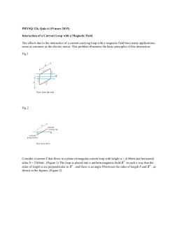


© Copyright 2026