
Electrodeposition and Characterization of CuTe and Cu2Te Thin Films
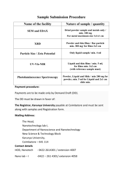
Electrodeposition and Characterization of CuTe and Cu2 Te Thin Films Fengchun Yang1, , Wenya He1 , Ye Zhang1 , Qing-Ya Zhu1 , Xin Zhang1,2, 1 Key Laboratory of Synthetic and Natural Functional M olecule Chemistry of M inistry of Education, College of Chemistry and M aterials Science, Northwest University, Xi'an, Shaanxi, 710069, China 2 Institute of Analytical Science, Northwest University, Shaanxi Provincial Key Laboratory of Electroanalytical Chemistry, Xi'an, Shaanxi, 710069, China ABSTRACT An electrodeposition method for fabrication of CuTe and Cu2 Te thin films are presented. The films’ growth is based on the epitaxial electrodeposition of Cu and Te alternately with different electrochemical parameter respectively. The deposited thin films were characterized by X-ray diffraction (XRD), field emission scanning electronic microscopy (FE-SEM) with an energy dispersive X-ray (EDX) analyzer, and FTIR studies. The results suggest that the epitaxial electrodeposition is an ideal method for deposition of compound semiconductor films for photoelectric applications. KeyWords: Epitaxy of thin films; Preparation; Semiconductors; Copper; Tellurium 1. Introduction Semiconducting compounds such as I–VI copper chalcogenides are widely used in the fabrication of photoconductive and photovoltaic devices[1, 2]. Copper based Corresponding author. E-mail address: [email protected] (F.C. Yang), Fax: +86 29 88302604 [email protected] (X. Zhang ), Fax: +86 29 88303448 1 chalcogenides exhibited the characteristics of a p-type semiconductor for the vacancies of copper, and are potential materials for widely applications. Especially, thin films of copper chalcogenides have been a subject of interest for many years mainly because of their wide range of applications in solar cells, superionic conductors, photodetectors, photothermal converters, electroconductive electrodes, microwave shielding, etc.[3-5]. Of these copper chalcogenides, copper telluride compounds have gained great interest owing to its superionic conductivity, direct band gap between 1.1 and 1.5 eV and large thermoelectric power. In the literature, a number of methods for preparation of Cux Se and Cux S thin films have been reported [5-10]. However, fabrication of CuTe thin films are much less studied to data [1, 11-14]. Copper telluride compounds (Cux Te, where x=1, 2 or between 1 and 2) were known to exist in a wide range of compositions and phases whose properties are controlled by the Cu:Te ratio, and can be grown by chemical bath deposition, co-evaporation and fusion method. Electrochemical atomic layer deposition [15-20] is considered as a controllable and simple deposition technique for homogeneous compound semiconductors on conductive substrates without annealing. The electrochemical atomic layer deposition was based on the alternated underpotential deposition which was a phenomenon of surface limited, so that the resulting deposit was generally limited to one atomic layer. Thus, each deposition cycle formed a single layer of the compound, and the number of deposition cycles controls the thickness of deposits[21-23]. In this paper, an epitaxial electrodeposition method for preparation of CuTe and Cu2 Te thin films on ITO substrates by controlling the solution conditions in contact with the deposit and the potential of the electrode is reported. The crystallographic structures of the obtained films are discussed on the basis of X-ray diffraction data. Field emission scanning electronic microscopy (FE-SEM) with an energy dispersive X-ray (EDX) analyzer shows investigation of morphology. Optical characteristics of the films are studied by FTIR. 2. Experime ntal 2 Electrochemical experiments were carried out using a CHI 660A electrochemical workstation (CH Instrument, U.S.A.). The deposition was performed in a three-electrode cell with a platinum wire as counter electrode and Ag/AgCl/sat. KCl as reference electrode. Indium doped tin oxide (ITO) glass slide (≈20 Ω/cm) was used as a working electrode. Prior to electrodeposition, the ITO substrate was ultrasonic cleaned with acetone, ethanol and water sequentially. All solutions were prepared with nanopure water purified by the Milli-Q system (Millipore Inc., nominal resistivity 18.2 MΩ cm), and all chemicals were analytical reagent grade. The oxygen was removed by blowing purified N 2 before each measurement, all of which were conducted at room temperature. The crystallographic structures of the thin films obtained were determined by XRD (Rigaku D/max-2400). The morphology are investigated by FE-SEM (Kevex JSM-6701F, Japan) equipped with an EDX analyzer. Glancing angle absorption measurements were performed using an FTIR spectrophotometer (Nicolet Nexus 670, USA). 3. Results and discussion 3.1. Thin film deposition 3.1.1. CuTe thin film deposition Fig.1 shows the cyclic voltammograms of ITO electrode in blank and Cu solution respectively. For CuTe film growth, H2 SO 4 were used as supporting electrolyte. From fig.1b, only one pair of redox peaks was observed at −0.34 V (C1) and 0.30 V (A1), corresponding to Cu2+ reduction to Cu, as reaction (1) shows. Cu2+ + 2e1− ↔ Cu (1) Fig. 2 shows the cyclic voltammograms of Cu-covered ITO electrode in 0.1 M H2 SO 4 and in 5 mM H2 TeO 3 +0.1 M H2 SO4 solutions. In these experiments, the potential scanning was started at 0 V to avoid the oxidative stripping of Cu. Similar to most literatures, two reduction peaks are seen: peak C2 at about -0.21 V based upon the four electrons process for Te reduction shown in reaction (1), and peak C3 at 3 about -0.46 V, which should be corresponded to bulk Te (0) reduction to Te2-, as reaction (2) shows. H2 TeO3 + 4H++ 4e1− ↔ Te +3H2 O (2) Te + 2H+ + 2e1−↔ H2 Te (3) Therefore, we applied -0.30 V as the electrodeposition potentials for Cu and -0.20 V for Te. Repeat electrodepositing Cu at -0.30 V and Te at −0.20 V for 15s alternately as many times as desired to grow epitaxial nanofilms of CuTe on ITO substrate. 3.1.2. Cu2 Te thin film deposition. For Cu2 Te film growth, KNO 3 were used as supporting electrolyte because Cu+ ions can’t exist in a strong acid solution like 0.1M H2 SO4 . Fig.3 shows the cyclic voltammograms of ITO electrode in blank KNO3 and Cu solution respectively. In Fig.3b, two well-defined cathodic peaks are located at −0.23 V (C4) and −0.51 V (C5), which are related to the formation of Cu2 O and reduction of Cu on the ITO substrate, as reaction (4) and (1) show [15]: 2Cu2++2e1−+2OH− ↔ Cu2 O+H2 O (4) Fig. 4 shows the cyclic voltammograms of Cu2 O-covered ITO electrode in 0.1 M KNO3 and in 5 mM H2 TeO 3 +0.1 M KNO 3 solutions. From Fig. 4b, two reduction peaks are also seen: peak C6 at about -0.35 V based upon the H2 TeO3 reduction to Te, and peak C7 at about -0.60 V corresponding to Te reduction to H2 Te, which immediately react with the underlying Cu2 O layer to form Cu2 Te, as reaction (5) shows. Cu2 O + H2 Te ↔ Cu2 Te + H2 O (5) Therefore, we applied -0.20 V as the electrodeposition potentials for Cu and -0.60 V for Te. Repeat electrodepositing Cu at -0.20 V and Te at −0.60 V for 15s alternately as many times as desired to grow epitaxial nanofilms of Cu2 Te on ITO substrate. 3.2. Thin film characterization 3.2.1. X-ray Investigations Identification of the obtained thin films was carried out using the X-ray 4 diffraction method. The recorded XRD patterns of deposited CuTe and Cu2 Te are presented in Fig. 5. Fig. 5a shows the XRD patterns of deposited CuTe film. The observed peak positions of the deposited CuTe film are in well agreement with those due to reflection from (0 1 1), (1 0 1) and (1 1 2) planes of the reported CuTe data with an orthorhombic structure (JCPDS 22-0252). The XRD pattern of deposited Cu2 Te film is presented in Fig. 5b. As can be seen, the analysis indicates that the deposited Cu2 Te film is in hexagonal structure, with the preferential orientation of (0 0 6) plane (JCPDS 49-1411). The average crystal size was estimated using the well-known Debye-Scherrer relationship: d 0.9 cos (6) where θ is the Bragg angle, λ is the X-ray wavelength, and β is the full width at half- maximum. It was found that the average crystal size of the deposited CuTe film is 92.11 nm, and Cu2 Te film was found to be about 36.84 nm, which are consistent with the SEM observation. 3.2.2. SEM observations The SEM micrographs of deposited CuTe and Cu2 Te films are shown in Fig. 6a and b, respectively, at 30,000× magnification. In deposited CuTe film (Fig. 3a), the grains are more distinct and of bigger size, while in Cu2 Te film (Fig. 3b), the grains are of smaller size, more compact with densely packed microcrystals. The EDX analysis was carried out only for Cu and Te. The average atomic percentage of Cu:Te in deposited CuTe film was 50.4:49.6. It is close to 1:1 stoichiometry. Similar results for Cu2 Te were 67.3: 32.7, close to 2:1 stoichiometry. 3.2.3. Optical measurements For optical characterization, FTIR spectra of deposited CuTe and Cu2 Te thin films were recorded. The optical band gap (Eg) for deposited CuTe and Cu2 Te thin films was calculated on the basis of the FTIR spectra, using the well-known relation 5 αhν = A(hν − Eg)1/2 (7) where A is the constant, Eg is the band gap, hν is the photon energy. Fig. 7 shows the variation of (αhν)2 with hν for deposited CuTe and Cu2 Te. By extrapolating straight line portion of (αhν)2 against hν plot to α=0, the optical band gap energy was found to be 1.51 eV for CuTe and 1.12 eV for Cu2 Te films, comparable with the value reported earlier for CuTe and Cu2 Te thin film[1, 16]. 4. Conclusion In this work, the Cu/Te ratio has been successfully controlled to prepare crystalline CuTe and Cu2 Te thin films on the ITO electrode via electrodeposition. The copper-tellurium films were epitaxial electrodeposited under layer-by-layer, potentiostatic conditions. XRD, SEM and IR studies of the deposited CuTe and Cu2 Te thin films confirm the high quality of the deposits, and demonstrate that the epitaxial electrodeposition is applicable to the deposition of stoichiometric nano films of copper-tellurium films of good quality. Acknowledge ment We gratefully acknowledge support from China Postdoctoral Science Foundation (No. 2013M532027), the National Natural Scientific Foundation of China (no.21301137 and 21405120), the New Teachers’ Fund for Doctor Stations, Ministry of Education (Grant no.20126101120012), and the Scientific Research Program Funded by Shaanxi Provincial Education Department (Grant nos.12JK0578 and 12JK0617). References [1] K. Neyvasagam, N. Soundararajan, Ajaysoni, G. S. Okram, V. Ganesan, “Low-temperature electrical resistivity of cupric telluride (CuTe) thin films ”, Phys. Status Solidi B, vol. 245, no. 1, pp. 77-81, 2008. 6 [2] O. M. Hussain, B. S. Naidu, P. J. Reddy, “Photovoltaic properties of n-CdS/p-Cu2Te thin film heterojunctions”, Thin Solid Films, vol. 193-194, pp. 777-781, 1990. [3] Q. Sun, J. W. Y. Lam, K. Xu, H. Xu, J. A. K. Cha, P. C. L. Wong, G. Wen, X. Zhang, X. Jing, F. Wang, B. Z. Tang, “Nanocluster-Containing Mesoporous Magnetoceramics from Hyperbranched Organometallic Polymer Precursors ”, Chem. Mater., vol. 12, no. 9, pp. 2617-2624, 2000. [4] M. Korzhuev, “Dufour effect in superionic copper selenide”, Phys. Solid State, vol.40, no. 2, pp. 217-219, 1998. [5] C. Nascu, I. Pop, V. Ionescu, E. Indrea, I. Bratu, “Spray pyrolysis deposition of CuS thin films”, Mater. Lett., vol.32, no. 2-3, pp.73-77, 1997. [6] S. R. Gosavi, N. G. Deshpande, Y. G. Gudage, R. Sharma, “Physical, optical and electrical properties of copper selenide (CuSe) thin films deposited by solution growth technique at room temperature”, J. Alloy. Compd., vol. 448, no. 1-2, pp. 344-348, 2008. [7] W. Wei, S. Zhang, C. Fang, S. Zhao, B. Jin, J. Wu, Y. Tian, “Electrochemical behavior and electrogenerated chemiluminescence of crystalline CuSe nanotubes”, Solid State Sci., vol.10, no. 5, pp. 622-628, 2008. [8] M. Dhanam, P. K. Manoj, R. R. Prabhu, “High-temperature conductivity in chemical bath deposited copper selenide thin films”, J. Cryst. Growth, vol.280, no. 3-4, pp. 425-435, 2005. [9] R. Córdova, H. Gómez, R. Schrebler, P. Cury, M. Orellana, P. Grez, D. Leinen, J. R. Ramos-Barrado, R. D. Río, “Electrosynthesis and Electrochemical Characterization of a Thin Phase of CuxS (x → 2) on ITO Electrode”, Langmui, vol.18, no.22, pp. 8647-8654, 2002. [10] S. Lindroos, A. Arnold, M. Leskel, “Growth of CuS thin films by the successive ionic layer adsorption and reaction method”, Appl. Surf. Sci., vol.158, no. 1-2, pp. 75-80, 2000. [11] J. Zhou, X. Wu, A. Duda, G. Teeter, S. H. Demtsu, “The formation of different phases of CuxTe and their effects on CdTe/CdS solar cells”, Thin Solid Films, vol.515, 7 no. 18, pp. 7364-7369, 2007. [12] S. Kashida, W. Shimosaka, M. Mori, D. Yoshimura, “Valence band photoemission study of the copper chalcogenide compounds, Cu2S, Cu2Se and Cu2Te”, J. Phys. Chem., Solids, vol. 64, no. 12, pp. 2357-2363, 2003. [13] F. Pertlik, “Vulcanite, CuTe: Hydrothermal synthesis and crystal structure refinement”, Miner. Petrol., vol. 71, no. 3-4, pp. 149-154, 2001. [14] K. Sridhar, K. Chattopadhyay, “Synthesis by mechanical alloying and thermoelectric properties of Cu2Te”, J. Alloy. Compd., vol. 264, no. 1-2, pp. 293-298, 1998. [15] X. Zhang, X. Shi, C. Wang, “Optimization of electrochemical aspects for epitaxial depositing nanoscale ZnSe thin films”, J. Solid State Electrochem. vol. 13, no. 1, pp. 469-475, 2009. [16] W. Zhu, X. Liu, H. Liu, D. Tong, J. Yang, J. Peng, “Coaxial heterogeneous structure of TiO2 nanotube arrays with CdS as a superthin coating synthesized via modified electrochemical atomic layer deposition”, J. Am. Chem. Soc., vol. 132, no. 36, pp. 12619-12626, 2010. [17] H. Kou, X. Zhang, Y. Jiang, J. Li, S. Yu, Z. Zheng, C. Wang, “Electrochemical atomic layer deposition of a CuInSe2 thin film on flexible multi- walled carbon nanotubes/polyimide nanocomposite membrane: Structural and photoelectrical characterizations”, Electrochim. Acta., vol. 56, no. 16, pp. 5575–5581, 2011 [18] D.O. Banga, R. Vaidyanathan, X. Liang, J.L. Stickney, S. Cox, U. Happeck, “Formation of PbTe nanofilms by electrochemical atomic layer deposition (ALD)”, Electrochim. Acta., vol. 53, no. 23, pp. 6988-6994, 2008. [19] F. Loglio, A.M. Telford, E. Salvietti, M. Innocenti, G. Pezzatini, S. Cammelli, F. D'Acapito, R. Felici, A. Pozzi, M.L. Foresti, “Ternary CdxZn1−xSe deposited on Ag (1 1 1) by ECALE: Electrochemical and EXAFS characterization”, Electrochim. Acta., vol. 53, no. 23, pp. 6978-6987, 2008. [20] X. Liang, N. Jayaraju, C. Thambidurai, Q. Zhang, J.L. Stickney, “Controlled Electrochemical Formation of GexSbyTez using Atomic Layer Deposition (ALD) ”, Chem. Mater., vol. 23, no. 3, pp. 1742-1752, 2011. 8 [21] D.M. Kolb, R. Kotz, K. Yamamoto, “Copper monolayer formation on platinum single crystal surfaces: Optical and electrochemical studies”, Surf. Sci. vol. 87, no. 1, pp. 20-30, 1979. [22] D.M. Kolb, “Reaction at the Liquid-Solid Interface : Volume 28 of the series, Comprehensive Chemical Kinetics Edited by R.G. Compton Elsevier, Amsterdam, 1989, 300pp. (also available from Elsevier, New York)”, Electrochim. Acta, vol. 37, no. 1, pp. 181, 1992. [23] U. Demir, C. Shannon, “Reconstruction of Cadmium Sulfide Monolayers on Au(100)”, Langmuir, vol. 12, no. 2, pp. 594-596, 1996. [24] W. Shang, X. Shi, X. Zhang, C. Ma, C. Wang, “Growth and characterization of electro-deposited Cu2O and Cu thin films by amperometric I–T method on ITO/glass substrate”, Appl. Phys. A-Mater., vol. 87, no. 1, pp. 129-135, 2007. [25] B. S. Farag, S. A. Khodier, “Direct and indirect transitions in copper telluride thin films”, Thin Solid Films, vol. 201, no. 2, pp. 231-240, 1991. 9 Figure captions Fig. 1. Cyclic voltammograms of ITO electrode in (a) 0.1 M H2 SO4 ; (b) 0.1 M H2 SO4 with 5 mM CuSO 4 . (Scan rate: 10 mV/s) Fig. 2. Cyclic voltammograms of Cu-covered ITO electrode in (a) 0.1 M H2 SO4 ; (b) 0.1 M H2 SO4 with 5 mM TeO 2 . (Scan rate: 10 mV/s) Fig. 3. Cyclic voltammograms of ITO electrode in (a) 0.1 M KNO3 ; (b) 0.1 M KNO3 with 5 mM CuSO 4 . (Scan rate: 10 mV/s) Fig. 4. Cyclic voltammograms of Cu2 O-covered ITO electrode in (a) 0.1 M KNO3 ; (b) 0.1 M KNO3 with 5 mM TeO 2 . (Scan rate: 10 mV/s) Fig. 5. XRD patterns of deposited CuTe (a) and Cu2 Te (b) films. Fig. 6. SEM micrograph of deposited CuTe (a) and Cu2 Te (b) films. Fig. 7. The dependence of (ahν)2 on hν for deposited CuTe (a) and Cu2 Te (b) films. 10 Figure(s) Fig. 1 11 Figure(s) Fig. 2 12 Figure(s) Fig. 3 13 Figure(s) Fig. 4 14 Figure(s) Fig. 5 15 Figure(s) Fig. 6 16 Figure(s) Fig. 7 17


© Copyright 2026