
Battery Fuel Gauge LSI for 1
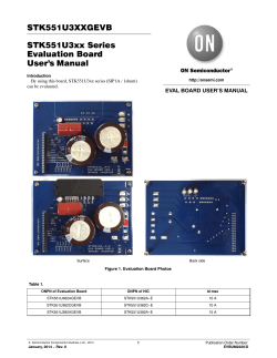
LC709203F CMOS LSI Battery Fuel Gauge LSI for 1-Cell Lithium-ion (Li+) www.onsemi.com Overview The LC709203F is an IC that measures the remaining power level of 1-cell lithium-ion (Li+) batteries used for portable equipment etc. This product reduces fuel gauge errors with a unique correction technology during measurement of battery temperature and voltage. This technology has inherent high precision without the need for an external sense resistor. Applications WDFN8 3x4, 0.65P Wireless Handsets Smartphones / PDA devices MP3 players Digital cameras Portable Game Players USB-related devices Features High accuracy of remaining battery power measurements Precision Voltage Measurement No external sense resistor Alert function Interface I2C Interface (up to 400 kHz supported) Low power consumption Corresponding battery models for various battery electrode materials Ports I2C communication pin : 2 (SDA, SCL) Battery temperature reading control pin : 1 (TSW) Analog voltage input pin for battery temperature : 1 (TSENSE) External alarm / Interrupt for Low-Battery warning : 1 (ALARMB) Power supply pin : 2 (VSS, VDD) Package form WDFN8 34, 0.65P : Pb-Free, Halogen Free type WLCSP9, 1.601.76 : Pb-Free, Halogen Free type WLCSP9, 1.60x1.76 * I2C Bus is a trademark of Philips Corporation. ORDERING INFORMATION See detailed ordering and shipping information on page 13 of this data sheet. © Semiconductor Components Industries, LLC, 2015 January 2015 - Rev. 7 1 Publication Order Number : LC709203F/D LC709203F Package Dimensions unit : mm WDFN8 3x4, 0.65P CASE 509AF ISSUE C L A B D L NOTES: 1. DIMENSIONING AND TOLERANCING PER ASME Y14.5M, 1994. 2. CONTROLLING DIMENSION: MILLIMETERS. 3. DIMENSION b APPLIES TO PLATED TERMINAL AND IS MEASURED BETWEEN 0.15 AND 0.30mm FROM THE TERMINAL TIP. 4. PROFILE TOLERANCE APPLIES TO THE EXPOSED PAD AS WELL AS THE LEADS. L1 DETAIL A ALTERNATE CONSTRUCTIONS DIM A A1 A3 b D D2 E E2 e L L1 E PIN ONE REFERENCE 2X EXPOSED Cu MOLD CMPD 0.10 C DETAIL B 0.10 C 2X ALTERNATE CONSTRUCTIONS TOP VIEW A (A3) DETAIL B 0.10 C SIDE VIEW A1 C XXXXX XXXXX AYWW SEATING PLANE 0.10 C A B A = Assembly Location Y = Year WW = Work Week = Pb-Free Package (Note: Microdot may be in either location) D2 DETAIL A 1 4 0.10 C A B 8X 0.00 0.05 0.20 REF 0.20 0.30 3.00 BSC 1.70 1.90 4.00 BSC 2.30 2.50 0.65 BSC 0.45 0.55 GENERIC MARKING DIAGRAM* 0.08 C NOTE 4 MILLIMETERS MIN MAX L *This information is generic. Please refer to device data sheet for actual part marking. E2 may or may not be present. 8 5 e/2 e 8X RECOMMENDED SOLDERING FOOTPRINT* b 1.96 0.10 C A B 0.05 C 8X 0.70 NOTE 3 BOTTOM VIEW 2.56 4.30 1 0.65 PITCH 8X 0.35 DIMENSIONS: MILLIMETERS *For additional information on our Pb-Free strategy and soldering details, please download the ON Semiconductor Soldering and Mounting Techniques Reference Manual, SOLDERRM/D. www.onsemi.com 2 LC709203F WLCSP9, 1.60x1.76 CASE 567JH ISSUE B E A B NOTES: 1. DIMENSIONING AND TOLERANCING PER ASME Y14.5M, 1994. 2. CONTROLLING DIMENSION: MILLIMETERS. 3. COPLANARITY APPLIES TO THE SPHERICAL CROWNS OF THE SOLDER BALLS. PIN A1 REFERENCE D DIM A A1 b D E e 0.05 C 2X 0.05 C 2X TOP VIEW BACKCOAT 0.10 C MILLIMETERS MIN MAX 0.51 −−− 0.09 0.19 0.20 0.30 1.60 BSC 1.76 BSC 0.50 BSC A RECOMMENDED SOLDERING FOOTPRINT* 0.08 C A1 A1 NOTE 3 C SIDE VIEW PACKAGE OUTLINE SEATING PLANE e 9X b 0.05 C A B e 0.50 PITCH C 0.03 C B 9X 0.25 0.50 PITCH DIMENSIONS: MILLIMETERS A 1 2 3 BOTTOM VIEW *For additional information on our Pb−Free strategy and soldering details, please download the ON Semiconductor Soldering and Mounting Techniques Reference Manual, SOLDERRM/D. www.onsemi.com 3 LC709203F Pin Assignment TSW Bottom view TSENSE Top view SDA WLCSP9, 1.60x1.76 “Pb-Free, Halogen Free Type” SCL WDFN8 3x4, 0.65P “Pb-Free, Halogen Free Type” 8 7 6 5 LC709203F VDD 3 4 ALARMB 2 VSS TEST 1 TSENSE TSW VDD SCL NC SDA TEST VSS C B A 3 ALARMB 2 1 Pin Function Pin Name I/O Description WDFN8 WLP9 1 1B TEST I 2 1A VSS - Connect to the - terminal of the battery. 3 3A VDD - Connect to the + terminal of the battery. 4 2A ALARMB O 5 3B TSW O Battery temperature reading control pin I Battery temperature analog voltage input pin 6 3C TSENSE Factory Test pin *Connect to VSS. Alert indication. An active low output used to indicate specified condition thresholds have been met. *When you do not use an alert function, please connect with VSS. (Note 3) (Note.1) 7 1C SDA I/O I2C data pin 8 2C SCL I/O I2C clock pin - 2B NC - Not used pin. *Recommend to connect to VSS. - EP - Exposed Pad, must not be connected. (Note.2) (Note 1) This pin provides power for the thermistor and goes high during a temperature read operation from Command code x08. (Note 2) If TSENSE is not used leave leads TSW and TSENSE disconnected, as in figure 4 and set bit 0 of command code register x16 low. If TSENSE is utilized connect as in figure 5 with resistor network and set bit 0 of command code register x16 high. (Note 3) ALARMB indicates a low RSOC, or an under voltage battery. www.onsemi.com 4 LC709203F Alert Function Configurable Alert Indicator Low RSOC Battery Under Voltage Alarm RSOC Function RSOC, Alarm Low RSOC (%) RSOC Alarm Low RSOC ALARMB terminal 12 11 10 9 8 7 6 5 4 3 2 1 0 Change the setting to 3% Block Diagram LC709203F SDA SCL TSW TSENSE PACK - I2C Interface Remaining Voltage Processing Unit Voltage Detect ALARMB PACK + www.onsemi.com 5 LC709203F Absolute Maximum Ratings at Ta = 25C, VSS = 0V Specification Parameter Symbol Pin/Remarks Conditions Unit VDD [ V ] Maximum supply VDD max VDD Input voltage VI (1) TSENSE Output voltage Vo (1) TSW Vo (2) ALARMB VIO (1) SDA, SCL Pd max WDFN8 voltage Input/output dissipation Operating ambient max 0.3 +6.5 0.3 VDD +0.3 0.3 VDD +0.3 0.3 V +5.5 Ta = 40 to +85C 480 mW WLP9 210 Topr temperature Storage ambient typ 0.3 voltage Allowable power min 40 +85 55 +125 C Tstg temperature Stresses exceeding those listed in the Maximum Ratings table may damage the device. If any of these limits are exceeded, device functionality should not be assumed, damage may occur and reliability may be affected. Allowable Operating Conditions at Ta = 40 to +85C, VSS = 0V Specification Parameter Symbol Pin/Remarks Conditions VDD [ V ] Operating supply VDD (1) VDD VIH (1) TSENSE VIH (2) ALARMB, SDA, SCL voltage Low level input VIL (1) TSENSE VIL (2) ALARMB, SDA, SCL voltage typ max 2.5 4.5 2.5 to 4.5 0.7VDD VDD 2.5 to 4.5 1.4 2.5 to 4.5 VSS voltage High level input min 2.5 to 4.5 unit V 0.25VDD 0.5 Functional operation above the stresses listed in the Recommended Operating Ranges is not implied. Extended exposure to stresses beyond the Recommended Operating Ranges limits may affect device reliability. www.onsemi.com 6 LC709203F Electrical Characteristics at Ta = 40 to +85C, VSS = 0V Specification Parameter Symbol Pin/Remarks Conditions Unit VDD[V] High level input IIH (1) SDA, SCL current VIN = VDD (including output transistor off min typ max 2.5 to 4.5 1 leakage current) Low level input IIL (1) SDA, SCL current VIN = VSS (including output transistor off A 2.5 to 4.5 1 IOH = 0.4 mA 3.0 to 4.5 VDD0.4 IOH = 0.2 mA 2.5 to 4.5 VDD0.4 IOL = 3.0 mA 3.0 to 4.5 0.4 IOL = 1.3 mA 2.5 to 4.5 0.4 leakage current) High level output VOH (1) TSW voltage VOH (2) Low level output voltage Hysteresis VOL (1) VOL (2) TSW, ALARMB, SDA, SCL VHYS(1) SDA, SCL CP All pins voltage Pin capacitance 2.5 to 4.5 0.1VDD 2.5 to 4.5 10 15 26 V Pins other than the pin under test VIN = VSS pF Ta = 25C Consumption IDD (1) Testing Mode 2.5 to 4.5 current IDD (2) Operational Mode 2.5 to 4.5 2 4.5 IDD (3) Sleep Mode 2.5 to 4.5 0.2 4 Ta = +25C 3.6 7.5 +7.5 2.5 to 4.5 20 +20 (Note 1) Voltage VME (1) measurement VME (2) accuracy VDD VDD Ta = 20C to +70C μA mV/cell Note 1 : Consumption current is a value in the range of 20C to +70C Product parametric performance is indicated in the Electrical Characteristics for the listed test conditions, unless otherwise noted. Product performance may not be indicated by the Electrical Characteristics if operated under different conditions. www.onsemi.com 7 LC709203F I2C Slave Characteristics at Ta = 40 to +85C, VSS = 0V Specification Parameter Symbol Pin/Remarks Conditions unit VDD[V] min Max Clock frequency TSCL SCL Bus free time between STOP TBUF SCL, SDA See Fig. 1. 1.3 s THD:STA SCL, SDA See Fig. 1. 0.6 s SCL, SDA See Fig. 1. 0.6 s 0.6 s 400 kHz condition and START condition Hold time (repeated) START condition First clock pulse is generated after this interval Repeated START condition TSU:STA setup time 2.5 to 4.5 STOP condition setup time TSU:STO SCL, SDA See Fig. 1. Data hold time THD:DAT SCL, SDA See Fig. 1. 0 Data setup time TSU:DAT SCL, SDA See Fig. 1. 100 ns Clock low period TLOW SCL 1.3 s Clock high period THIGH SCL 0.6 s Clock/data fall time TF SCL, SDA 20 + 0.1CB 300 ns Clock/data rise time TR SCL, SDA 20 + 0.1CB 300 ns tR tF t LOW t HD:STA s 0.9 t HD:STA t HD:DAT t HIGH t SU:DAT t SU:STA t SU:STO t BUF P S S Figure 1 I2C Timing www.onsemi.com 8 P LC709203F Discharge Characteristics Figure 2 Discharge Characteristics by Temperature Change Figure 3 Discharge Characteristics by Load Change www.onsemi.com 9 LC709203F Communication Protocol Communication protocol type : I2C Frequency : to 400kHz IC address : 0x16 ( It becomes "0001011X" when you write a binary, because the slave address is 7 bits. [ X ]=Rd/Wr. ) Bus Protocols S Sr Rd Wr A N P CRC-8 : : : : : : : : : Start Condition Repeated Start Condition Read (bit value of 1) Write (bit value of 0) ACK (bit value of 0) NACK (bit value of 1) Stop Condition Slave Address to Last Data (CRC-8-ATM : ex.3778mV : 0x16,0x09,0x17,0xC2,0x0E 0x86) Master-to-Slave : Slave-to-Master : Continuation of protocol … Read Word Protocol S Slave Address Wr A Command Code A Sr Slave Address Rd A Data Byte Low A … Data Byte High … A CRC-8 N P *When you do not read CRC -8, there is not the reliability of data. CRC-8-ATM ex : (5 bytes) 0x16,0x09,0x17,0xC2,0x0E 0x86 Write Word Protocol S Slave Address Data Byte Low A Wr A Command Code Data Byte High A A … CRC-8 A P *When you do not add CRC -8, the Written data (Data byte Low/High) become invalid. CRC-8-ATM ex : (4 bytes) 0x16, 0x09, 0x55, 0xAA 0x3B Command Code Slave Functions Access Range Unit Description Initial Value 0x06 Thermistor β R/W 0x0000 to 0xFFFF β Sets selected thermistor constant value β 0x0D34 0x07 Initial RSOC W 0xAA55 Value Sets RSOC to its initial value - R 0x0000 to 0xFFFF (Thermistor Mode) 0x09E4 to 0x0D04 (Via I2C) 0.1°K (0.0C = 0x0AAC) Displays the value of the Cell Temperature W 0x0BA6 (25C) Displays the value of the Cell Voltage - 0x08 Cell Temperature 0x09 Cell Voltage R 0x0000 to 0xFFFF mV 0x0A Current Direction R/W 0x0000: Auto 0x0001: Charge 0xFFFF: Discharge Function that allows Fuel Gauge to report RSOC in various conditions 0x0B APA (Adjustment Pack Application) R/W 0x0000 to 0xFFFF Value 0x0C APT (Adjustment Pack Thermistor) R/W 0x0000 to 0xFFFF Delay time to compensate thermistor value due to parallel capacitor & Pull-Up Resistor 0x001E 0x0D RSOC ( Relative State of Charge) R 0x0000 to 0x0064 % - 0x0F FG unit R 0x0000 to 0x03E8 Displays remaining capacity of battery based on a 0-1000 scale - 0x11 IC Version R 0x0000 to 0xFFFF Version from 0x2717 0x12 Default or Alternative Profile Select R/W 0x0000 or 0x0001 Allows to choose between stored battery profiles (Please refer to lower list) 0x13 Alarm Low RSOC R/W 0x0000 to 0x0064 % (activate under) Allows the assignment of an alarm with a given RSOC value 0x0008 0x14 Alarm Low Cell Voltage R/W 0x0000 to 0xFFFF mV (activate under) Allows the assignment of an alarm with a given voltage value 0x0000 0x15 IC Power Mode R/W 0x0000 to 0x0002 0x0000 : Testing Mode 0x0001 : Operational Mode 0x0002 : Sleep Mode 0x0002 0x16 Thermistor Status Bit R/W 0 : disable 1 : enable 0x0000 0x1A Profile Number R bit 0 : Thermistor Mode bit 1 to 15 : Reserved (fix 0) 0x0301 or 0x0504 Compensate for total impedance between the Battery and Fuel Gauge Displays RSOC value based on a 0-100 scale Displays the IC version Displays whether thermistor is enabled or disabled Displays battery profiles uploaded 301 or 504 (Please refer to lower list) www.onsemi.com 10 0x0000 - 0x0000 - LC709203F Number Of The Parameter Type Of The Battery LC709203F-01 LC709203F-04 Normal Voltage3.8V, Charge Voltage 4.35V 0x0301 Normal Voltage3.7V, Charge Voltage 4.2V ICR18650-26H (SAMSUNG) 0x0504 UR18650ZY (Panasonic) Change Of The Parameter 0x0000 0x0001 0x0000 0x0001 RSOC = Relative State Of Charge 0xXXXX = Hexadecimal notation (Note) Initialization from Host : - The IC will initialize reading the battery temperature until Initialization sequence with serial port is executed. (Please see EVB manual for sequences.) Control from Host : - The Remaining State of Charge (RSOC) is normally read periodically. - To read temperature the part will need a sequence of instructions and then returned to RSOC reading. www.onsemi.com 11 LC709203F Application Circuit Example Figure 4 Example of an application schematic using LC709203F (not use temperature detection function) System Vdd 10kΩ 10kΩ Vdd I2C Bus Master TSW TSENSE Battery Pack SDA SCL T ASIC ALARMB VDD VSS TEST LC709203F 10kΩ Interrupt Input 1uF PACK- Vss PACK+ System System Vss Figure 5 Example of an application schematic using LC709203F (use temperature detection function) System Vdd 10kΩ 10kΩ Vdd I2C Bus Master Battery Pack 10KΩ (s a me as thermistor resistance value) T TSW SDA SCL thermistor TSENSE 100Ω 10kΩ ASIC ALARMB VDD VSS TEST LC709203F Interrupt Input 1uF PACK- 10kΩ Vss PACK+ System System Vss www.onsemi.com 12 LC709203F ORDERING INFORMATION Device Package Shipping (Qty / Packing) LC709203FQH-01TWG WDFN8 3x4, 0.65P (Pb-Free / Halogen Free) 2000 / Tape & Reel LC709203FQH-02TWG WDFN8 3x4, 0.65P (Pb-Free / Halogen Free) 2000 / Tape & Reel LC709203FQH-03TWG WDFN8 3x4, 0.65P (Pb-Free / Halogen Free) 2000 / Tape & Reel LC709203FQH-04TWG WDFN8 3x4, 0.65P (Pb-Free / Halogen Free) 2000 / Tape & Reel LC709203FXE-01MH WLCSP9, 1.60x1.76 (Pb-Free / Halogen Free) 5000 / Tape & Reel LC709203FXE-02MH WLCSP9, 1.60x1.76 (Pb-Free / Halogen Free) 5000 / Tape & Reel LC709203FXE-03MH WLCSP9, 1.60x1.76 (Pb-Free / Halogen Free) 5000 / Tape & Reel LC709203FXE-04MH WLCSP9, 1.60x1.76 (Pb-Free / Halogen Free) 5000 / Tape & Reel (Note) The type of battery affects the performance to some degree. Contact your sales team for assistance in choosing the correct model. ON Semiconductor and the ON logo are registered trademarks of Semiconductor Components Industries, LLC (SCILLC) or its subsidiaries in the United States and/or other countries. SCILLC owns the rights to a number of patents, trademarks, copyrights, trade secrets, and other intellectual property. A listing of SCILLC’s product/patent coverage may be accessed at www.onsemi.com/site/pdf/Patent-Marking.pdf . SCILLC reserves the right to make changes without further notice to any products herein. SCILLC makes no warranty, representation or guarantee regarding the suitability of its products for any particular purpose, nor does SCILLC assume any liability arising out of the application or use of any product or circuit, and specifically disclaims any and all liability, including without limitation special, consequential or incidental damages. “Typical” parameters which may be provided in SCILLC data sheets and/or specifications can and do vary in different applications and actual performance may vary over time. All operating parameters, including “Typicals” must be validated for each customer application by customer’s technical experts. SCILLC does not convey any license under its patent rights nor the rights of others. SCILLC products are not designed, intended, or authorized for use as components in systems intended for surgical implant into the body, or other applications intended to support or sustain life, or for any other application in which the failure of the SCILLC product could create a situation where personal injury or death may occur. Should Buyer purchase or use SCILLC products for any such unintended or unauthorized application, Buyer shall indemnify and hold SCILLC and its officers, employees, subsidiaries, affiliates, and distributors harmless against all claims, costs, damages, and expenses, and reasonable attorney fees arising out of, directly or indirectly, any claim of personal injury or death associated with such unintended or unauthorized use, even if such claim alleges that SCILLC was negligent regarding the design or manufacture of the part. SCILLC is an Equal Opportunity/Affirmative Action Employer. This literature is subject to all applicable copyright laws and is not for resale in any manner. www.onsemi.com 13


© Copyright 2026