
Call for Abstracts
AVS
American Vacuum Society
125 Maiden Lane, 15th Floor
New York, NY 10038
Tel: 212-248-0200
AVS 62 Call For Abstracts
T
he AVS 62nd International
Division/Group Programs
Symposium and Exhibition fosters n Advanced Surface Engineering
an interdisciplinary environment
n Applied Surface Science
featuring a plenary, parallel topical
n Biomaterial Interfaces & Biomaterials
sessions from AVS technical divisions,
Plenary
technology groups, and focus topics, poster
sessions, and an equipment exhibition.
n Electronic Materials & Processing
Check out the AVS Technical Library for n Magnetic Interfaces & Nanostructures
Past Symposia Virtual Programs and n Manufacturing Science & Technology
Presentations on Demand.
n MEMS and NEMS
An extensive array of tools, equipment,
service, and publications will be displayed n Nanometer-scale Science & Technology
at the Exhibit from Tuesday morning until n Plasma Science & Technology
Thursday afternoon.
n Surface Science
Short courses and Tutorials that pron Thin Films
vide specialized training in specific areas
n Vacuum Technology
of vacuum science and related technologies
will be offered.
Focus TopicS & Other Sessions
Division/Group/Focus Topic Awards and n 2D Materials
Travel Grants are being solicited.
n Accelerating Materials Discovery for
Global Competitiveness
n Actinides & Rare Earths
n Additive Manufacturing/3D Printing
Invited Speakers
300+ Invited Speakers,
including:
Judy Cha, Yale University
Plenary Speaker:
Robert S. Chau,
Intel Senior Fellow and
Director of Transistor Research
and Nanotechnology in the
Technology and Manufacturing
Group at Intel Corporation,
Li-Chyong Chen, National
Taiwan University
“Electronic Materials Research
and Development for Future
Computation and System On
Chip Applications”
Eshraq Al Dmour, Max IV, Lund
University, Sweden
Donna Chen, University of
South Carolina
Rowena Crockett, ETH
Shane Cybart, University of
California, San Diego
Melissa Denecke, University of
Manchester, United Kingdom
of Great Britain and Northern
Ireland
Phill Dickens, University of
Nottingham, UK
Jennifer Fielding, AFRL (NAMII)
n
Abstract Deadline: May 4, 2015
Complete Details at www.avs.org
Jacob Israelachvili, University of Buddy D. Ratner, University of
California, Santa Barbara
Washington
Kimberly Turner, University of
California, Santa Barbara
Thomas Jaramillo, Stanford
University
Arend van der Zande, Columbia
University
Noo Li Jeon, Seoul National
University, Korea
Matt Kowitt, Stanford Research
Systems
Young Kuk, Seoul National
University, Korea
Ralf Richter, CIC biomaGUNE
Debra Rolison, Naval Research
Laboratory
Michael Roukes, California
Institute of Technology
Jean-Luc Rouviere, CEA-Leti,
France
Zhiyong Ma, Intel
Simone Ruggeri, EPFL,
Switzerland
Hari Manoharan, Stanford
University
Miquel Salmeron, Lawrence
Berkeley National Lab
Yongfeng Mei, Fudan University Robert Schlogol, FHI, Max
Planck Society, Germany
Philip Messersmith, University
Anna Fontcuberta i Morral,
of California, Berkeley
Ecole Polytechnique Fédérale de
Masaaki Nagatsu, Shizuoka
Anna Balazs, University of
Lausanne
University, Japan
Pittsburgh
Hajo Freund, Fritz Haber
Olga Ovchinnikova, Oak Ridge
James Batteas, Texas A&M
Institute, Germany
National Laboratory
Geoff Beach, MIT
Krzysztof Gofryk, Idaho
Nam-Gyu Park, Sungkyunkwan
Stacey Bent, Stanford University National Laboratory
University, Korea
Stefan Bonetti, University of
Roy Gordon, Harvard University
Kristin Persson, Lawrence
Stockholm, Sweden
David Graves, University of
Berkeley National Laboratory
Bill Bottoms, Third Millenium
California, Berkeley
David Pui, University of
Test Solutions
Birgit Hagenhoff (ToF-SIMS),
Minnesota
Mark Bradley, University of
TASCON, GmbH, Germany
Ramamurthy Ramprasad,
Edinburgh, UK
Suvi Haukka, ASM
University of Connecticut
Ken Burch, Boston College
Microchemistry, Finland
Alok Ranjan, TEL Technology
Cristina Canal, Universitat
Tony Heinz, Columbia University Center of America
Politècnica de Catalunya, Spain
Dieter Isheim, Northwestern
University
Ana Claudia Arias, UC Berkeley
Atom Probe Tomography
Energy Frontiers
n Exhibitor Technology Spotlight
n Helium Ion Microscopy
n In-Situ Spectroscopy & Microscopy
n IPF on Mesoscale Science and Technology
of Materials and Metamaterials
n Materials Characterization in the
Semiconductor Industry
n Novel Trends in Synchrotron & FEL-Based
Analysis
n Scanning Probe Microscopy
n Selective Deposition as an Enabler of
Self-Alignment
n Spectroscopic Ellipsometry
n Surface Modification of Materials by
Plasmas for Medical Purposes
n Tribology
n
Daniel Schreiber, Pacific
Northwest National Laboratory
Dario Stacchiola, Chemistry
Department, Brookhaven
National Laboratory
Hans-Peter Steinrueck,
University of ErlangenNuremberg, Germany
Adrienne Stiff-Roberts, Duke
University
Yayoi Takamura, University of
California at Davis
Shida Tan, Intel Corporation
Mauritius C.M. van De Sanden,
DIFFER, The Netherlands
Tonya Vitova, Karlsruhe Institute
of Technology, Germany
Virginia Wheeler, Naval
Research Laboratory
Bernd Winter, HelmholtzZentrum Berlin für
Materialien und Energie/
Elektronenspeicherring BESSY
II, Berlin, Germany
Charles Winter, Wayne State
University
Tom Wirtz, Centre de Recherche
Public – Gabriel Lippmann,
Luxembourg
Grace Xing, Cornell University
Eli Yablonovitch, University
California Berkeley
Oleg Yazyev, Ecole
Polytechnique Fédérale de
Lausanne, Switzerland
Bilge Yildiz, MIT
Pengpeng Zhang, Michigan
State University
Jeffery Terry, Illinois Institute of
Eva Zurek, University at
Technology
Buffalo-SUNY
Mathias Thuvander, Chalmers,
Sweden
The AVS 62nd International Symposium & Exhibition
On behalf of the AVS community, we invite you to submit an abstract to the AVS 62 nd International
Symposium and Exhibition that will take place the week of October 18-23, 2015 in San Jose, California.
We are fortunate to have Dr. Robert Chau, Director of Transistor Research and Nanotechnology in the
Technology and Manufacturing Group at Intel Corporation, kick off the Symposium with a Plenary Lecture on
“Electronic Materials Research and Development for Future Computation and System-On-Chip Applications.”
This topic is appropriate because we will be in the heart of Silicon Valley and because so much of the surface,
materials, processing, and interface research that will be presented at the meeting is motivated by applications.
We are also fortunate this year to have the AIP Industrial Physics Forum on “Mesoscale Science and
Technology of Materials and Metamaterials.” Several of the divisions and focus topics will run sessions to
complement the all-invited IPF sessions. The other focus topics that will be featured at this meeting are 2D
Materials, Additive Manufacturing, Materials Characterization in the Semiconductor Industry, Selective
Deposition as an Enabler of Self-Alignment, In situ Spectroscopy and Microscopy, Helium Ion Microscopy,
Scanning Probe Microscopy, Spectroscopic Ellipsometry, Actinides and Rare Earths, Atom Probe Tomography,
Synchrotron Analysis, Energy Frontiers, Accelerating Materials Discovery for Global Competitiveness,
Tribology, and Surface Modification by Plasmas for Medicine. These topics will complement our traditional
strong core on fundamental surface science and interfacial phenomena, applied surface science, surface
engineering, micro- and nano-electronics, nanometer science and technology, manufacturing science and
technology, thin films, plasma science and technology, micro- and nano-electromechanical systems, electronic
and magnetic materials, biomaterials, and vacuum science and technology.
This year is the 30th anniversary of the Applied Surface Science Division and several invited talks are planned
to mark that milestone. Apropos of our location, several sessions are planned to gain different perspectives on
the question “More Moore or More than Moore?” which will guide much of the development in the integrated
circuit industry in the near future. We anticipate running 15 parallel sessions each day and devoting two
evenings to poster sessions where we can debate some of the themes that will be presented during the meeting.
We are planning a large equipment and product exhibit where the latest vacuum technology will be on display
that makes cutting edge science possible. We have the good fortune to end the week with the IUVSTA meeting
where prominent speakers from all over the world will review the latest breakthroughs in our core science and
technology areas.
As you browse the Call for Abstracts, we are certain that you will find many sessions that will be of interest,
serve as the best venue for presenting your research in 2015, and provide ideas to start in new directions. We
encourage you to participate in this year’s symposium by submitting an abstract before the deadline on Monday,
May 4th.
We look forward to receiving your abstract and welcoming you to AVS 62 in San Jose!
Anthony J. Muscat
2015 Program Chair
Lisa Porter
2015 Program Vice-Chair
1
P R O G R A M
Program Chair
Anthony Muscat
University of Arizona
[email protected]
Program Vice-Chair
Lisa M. Porter
Carnegie Mellon University
[email protected]
2D Materials Focus Topic
Co-Chair: Bolotin, Kirill, Vanderbilt Univ.
Co-Chair: Gunlycke, Daniel, Naval
Research Laboratory
Co-Chair: Oleynik, Ivan, University of
South Florida
Borunda, Mario, Oklahoma State Univ.
Castellanos Gomez, Andres, Delft
University of Technology
Chhowalla, Manish, Rutgers University
Feng, Philip, Case Western Reserve Univ.
Lau, ChunNing(Jeanie), University of
California, Riverside
Lay, Marcus, The Cooper Union for the
Advancement of Science and Art
Le Lay, Guy, Aix-Marseille Univ., France
Ohta, Taisuke, Sandia National Labs
Osgood, Richard, Columbia University
Osterwalder, Juerg, Univ. of Zurich,
Switzerland
Park, Jiwoong, Cornell University
Schuller, Jon, UC Santa Barbara
Xu, Xiaodong, University of Washington
C O M M I T T E E
Durakiewicz, Tomasz, Los Alamos
National Laboratory
Geeson, David, AWE, UK
Havela, Ladislav, Charles University,
Czech Republic
Petit, Leon, Daresbury Laboratory, UK
Szakal, Christopher, National Institute of
Standards and Technology (NIST)
Szulczewski, Greg, The Univ. of Alabama
Additive Manufacturing/3D Printing
Co-Chair: Smentkowski, Vincent, General
Electric Global Research Center
Co-Chair: Svedberg, Erik B., The National
Academies
Dekker, Carl, Met-L-Flo Inc.
Dong, Xia, Eli Lilly and Company
Fitz-Gerald, James, University of Virginia
Ghita, Oana, Univ. of Exeter, UK of Great
Britain and Northern Ireland
Orringer, Neal, 3D Systems
Rogers, Bridget R., Vanderbilt University
Whiting, Gregory, Palo Alto Research Ctr
Biomaterial Interfaces
Chair: Leggett, Graham, University of
Sheffield, UK
Allen, Stephanie, The University of
Nottingham, UK
Baio, Joe, Oregon State University
Canavan, Heather, Univ. of New Mexico
Chi, Eva, University of New Mexico
Graham, Daniel, Univ. of Washington
Hanley, Luke, Univ. of Illinois at Chicago
Koelsch, Patrick, Univ. of Washington
Latour, Robert, Clemson University
Reviakine, Ilya, Karlsruhe Institute of
Technology, Germany
Rosenhahn, Axel, Ruhr-University
Bochum, Germany
Biomaterials Plenary Session
Chair: Leggett, Graham, University of
Sheffield, UK
Electronic Materials and Processing
Chair: King, Sean, Intel Corporation
Antonelli, Andy, Lam Research
Advanced Surface Engineering
Conley, Jr., John F., School of Electrical
Chair: Stueber, Michael, Karlsruhe
Engineering and Computer Science,
Institute of Technology, Germany
Oregon State University, Corvallis OR
Barankova, Hana, Uppsala Univ., Sweden
Daniels-Race, Theda, Louisiana State Univ.
Franz, Robert, Montanuniversität Leoben,
Dietz, Nikolaus, Georgia State University
Austria
Durbin, Steve, Western Michigan University
Klemberg-Sapieha, Jolanta, Ecole
Filler, Michael, Georgia Institute of Tech.
Polytechnique de Montreal, Canada
Gupta, Jay, Oho State University
Voevodin, Andrey, Air Force Research Lab
Han, Sang M., University of New Mexico
Hilton, Jessica, Mantis Deposition
Applied Surface Science
Accelerating Materials Discovery for
Hinkle, Christopher, Univ. of Texas at Dallas
Chair:
Lloyd,
Kathryn,
DuPont
Corporate
Global Competitiveness Focus Topic
Kim, Hyun Jung, NASA Langley
Center
for
Analytical
Sciences
Chair: Rahman, Talat, University of
Kummel, Andrew C., University of
Dong,
Xia,
Eli
Lilly
and
Company
Central Florida
California at San Diego
Gaskell,
Karen,
University
of
Maryland,
Co-Chair: Madsen, Lynnette, National
Mohney,
Suzanne, Pennsylvania State Univ.
College
Park
Science Foundation (NSF)
Myers-Ward, Rachael, U.S. Naval Research Lab.
Ohlhausen, James A. (Tony), Sandia
Alexander, Morgan, The University of
Rockett, Angus, University of Illinois at
National Laboratories
Nottingham, UK
Pacholski, Michaeleen, The Dow Chemical Urbana Champaign
Colombo, Luigi, Texas Instruments
Schultz, Brian, Raytheon
Company
de Leeuw, Nora, University College
Tischler, Joseph G., U.S. Naval Research Lab.
Stickle,
William,
Hewlett
Packard
London, UK
Whiting, Gregory, Palo Alto Research Ctr.
Szakal,
Christopher,
National
Institute
of
Dowben, Peter, Univ. of Nebraska-Lincoln
Zollner, Stefan, New Mexico State Univ.
Standards
and
Technology
(NIST)
Fischer, Peter, Lawrence Berkeley National
Tyler,
Bonnie,
National
Physical
Laboratory
Energy Frontiers Focus Topic
Laboratory (NPL), UK
Jones, Sean, OSTP/NSF
Chair: Baxter, Jason, Drexel University
Ventrice, Jr., Carl, Univ. at Albany-SUNY
Mueller, Tim, Johns Hopkins University
Aydil, Eray, University of Minnesota
Rogers, Bridget R., Vanderbilt University
Bent, Stacey, Stanford University
Atom Probe Tomography Focus Topic
Soukhojak, Andrey, The Dow Chemical
Filler, Michael, Georgia Institute of Tech.
Chair: Devaraj, Arun, Pacific Northwest
Company
Hinkle, Christopher, Univ. of Texas at Dallas
National Laboratory
Warren, James, National Institute of
Ohlhausen, James A. (Tony), Sandia
Bagot, Paul, Oxford University, UK
Standards and Technology (NIST)
National Laboratories
Cairney, Julie, Univ. of Sydney, Australia
Ramana,
Chintalapalle, University of
Perea,
Daniel,
Pacific
Northwest
National
Actinides and Rare Earths Focus Topic
Texas
at
El Paso
Laboratory
Chair: Tobin, James, Lawrence Livermore
Stueber,
Michael,
Karlsruhe Institute of
Prosa,
Ty,
CAMECA
National Laboratory
Technology,
Germany
Thevuthasan,
Suntharampillai,
Qatar
Bagus, Paul, University of North Texas
Environ. and Energy Res. Institute, Qatar Wei, David, University of Florida
Booth, Corwin, Lawrence Berkeley
Vurpillot, Francois, Univ. of Rouen, France
National Laboratory
2
Dhayal, Marshal, CSIR Centre for Cellular
and Molecular Biology (CCMB), India
Ghodssi, Reza, University of Maryland,
Helium Ion Microscopy Focus Topic
College Park
Chair: Hlawacek, Gregor, HelmholtzGousev, Evgeni, Qualcomm MEMS
Zentrum Dresden - Rossendorf, Germany
Technologies, Inc.
Co-Chair: Gölzhäuser, Armin, University
Hiebert, W.K., University of Alberta and
of Bielefeld, Germany
The National Institute for
Livengood, Richard, Intel Corporation
Nanotechnology, Canada
Notte, John A., Carl Zeiss Microscopy
Ilic, Robert, National Institute of Standards
and Technology (NIST)
In-Situ Spectroscopy and Microscopy
Kotru,
Sushma, The Univ. of Alabama
Focus Topic
Krylov, Slava, Tel Aviv University, Israel
Co-Chair: Nonnenmann, Stephen,
Maboudian, Roya, University of California
University of Massachusetts - Amherst
Co-Chair: Tao, Franklin (Feng), University at Berkeley
Metzler, Meredith, Cornell University
of Notre Dame
Co-Chair: Yang, Judith, Univ. of Pittsburgh Ng, Tse Nga (Tina), PARC (Palo Alto
Research Center), a Xerox Company
Co-Chair: Yu, Xiao-Ying, Pacific
Sumant, Anirudha, Argonne National Lab
Northwest National Laboratory
Thundat, Thomas, University of Alberta
IPF on Mesoscale Science and
and The National Institute for
Technology of Materials and
Nanotechnology, Canada
Metamaterials (IPF)
Tian, Wei-Cheng, National Taiwan
Co-Chair: Ludeke, Rudy, IBM Emeritus
University, Taiwan, Republic of China
Co-Chair: Rogers, Bridget R., Vanderbilt
Nanometer-scale Science and Technology
University
Chair: Nogami, Jun, University of Toronto,
Murday, James, University of Southern
Canada
California
Arnault, Jean-Charles, CEA LIST, France
Magnetic Interfaces and Nanostructures Baykara, Mehmet Z., Bilkent University
Chair: Szulczewski, Greg, The University
Borovsky, Brian P., St. Olaf College
of Alabama
Burnham, Nancy, Worcester Polytechnic
Donath, Markus, Muenster Univ., Germany
Institute
Enders, Axel, Univ. of Nebraska Lincoln
Chang, Chan-Yuen, National Tsing Hua
Ohldag, Hendrik, SLAC National
University
Accelerator Laboratory
Chang, Huan-Cheng, Academia Sinica,
Taiwan
Manufacturing Science and Technology
Cohen, Sidney, Weizmann Institute of
Chair: Rogers, Bridget R., Vanderbilt
Science, Israel
University
Evoy, Stephane, University of Alberta
Butler, Stephanie, Texas Instruments
Henry, Larry, Southern University
Diebold, Alain, SUNY College of
and A&M College
Nanoscale Science and Engineering
Ocola, Leonidas, Argonne National Lab.
Hu, Liangbing, University of Maryland,
Prater, Craig, Anasys Instruments
College Park
Murday, James, Univ. of Southern California Robinson, Jeremy, Naval Research Lab.
Seifu, Dereje, Morgan State University
Rubloff, Gary, University of Maryland,
Shenderova, Olga, Adámas
College Park
Svedberg, Erik B., The National Academies Nanotechnologies Inc.
Wei, David, University of Florida
Materials Characterization in the
Willey, Trevor, Lawrence Livermore
Semiconductor Industry Focus Topic
National Laboratory
Chair: van der Heide, Paul,
Novel Trends in Synchrotron and FELGLOBALFOUNDRIES, NY, USA
Co-Chair: Diebold, Alain, SUNY College Based Analysis Focus Topic
Chair: Rudolf, Petra, University of
of Nanoscale Science and Engineering
Groningen, The Netherlands
MEMS and NEMS
Dürr, Herrmann, Stanford University
Chair: Feng, Philip, Case Western Reserve Mårtensson, Nils, Uppsala Univ., Sweden
University
Plasma Science and Technology
Co-Chair: Burkett, Susan, The University
Chair: Joseph, Eric A., IBM Research
of Alabama
Division, T.J. Watson Research Center
Blain, Matthew, Sandia National Lab.
Davis, Robert, Brigham Young University Agarwal, Ankur, Applied Materials Inc.
Agarwal, Sumit, Colorado School of Mines
Exhibitor Technology Spotlight
Chair: DeGennaro, Jeannette, AVS
2
Booth, Jean-Paul, LPP-CNRS, Ecole
Polytechnique, France
Chang, Jane P., University of California at
Los Angeles
Despiau-Pujo, Emilie, LTM, France
Hamaguchi, Satoshi, Osaka Univ., Japan
Hsu, Cheng-Che, National Taiwan
University, Taiwan, Republic of China
Huffman, Craig, Sematech
Johnson, Erik, LPICM-CNRS, Ecole
Polytechnique, France
Nozawa, Toshihisa, Tokyo Electron Ltd., Japan
O'Connell, Deborah, University of York, UK
Park, Chanro, GLOBALFOUNDRIES
Reniers, François, Université Libre de
Bruxelles, Belgium
Sankaran, Mohan, Case Western Reserve Univ.
Sriraman, Saravanapriyan, Lam Research Corp
Srivastava, Aseem K., Applied Materials, Inc.
Tatsumi, Tetsuya, Sony Corporation, Japan
van de Sanden, Mauritius C.M., Dutch
Institute for Fundamental Energy
Research (DIFFER), Netherlands
Vitale, Steven, MIT Lincoln Laboratory
Wolden, Colin, Colorado School of Mines
Yeom, Geun Young, Sungkyunkwan
University, Republic of Korea
Scanning Probe Microscopy Focus Topic
Chair: Li, An-Ping, ORNL
Co-Chair: Allen, Stephanie, The University
of Nottingham, UK
Co-Chair: de Lozanne, Alex, University of
Texas at Austin
Co-Chair: Kim, Tae-Hwan, Pohang Univ.
of Science and Tech., Republic of Korea
Co-Chair: Nogami, Jun, University of
Toronto, Canada
Co-Chair: Ventrice, Jr., Carl, University at
Albany-SUNY
Selective Deposition as an Enabler of
Self-Alignment Focus Topic
Chair: Clendenning, Scott, Intel
Chabal, Yves, University of Texas at Dallas
Fischer, Pamela, ASM
Ma, Paul, Applied Materials, Inc.
Parsons, Gregory, North Carolina State Univ.
Smythe, John, Micron Technology
Spectroscopic Ellipsometry Focus Topic
Chair: Hofmann, Tino, University of
Nebraska-Lincoln
Aspnes, David, North Carolina State Univ
Creatore, Mariadriana, Eindhoven
University of Technology, Netherlands
Diebold, Alain, SUNY College of
Nanoscale Science and Engineering
Dong, Xia, Eli Lilly and Company
Filler, Michael, Georgia Institute of Tech.
Fujiwara, Hiroyuki, Gifu Univ., Japan
Hilfiker, James, J.A. Woollam Co., Inc.
Hingerl, Kurt, University Linz, Austria
Liu, Shiyuan, Huazhong University of
Science and Technology, China
Losurdo, Maria, University Bari, Italy
Schubert, Mathias, University of NebraskaLincoln
van der Heide, Paul,
GLOBALFOUNDRIES, NY, USA
Wormeester, Herbert, University of
Twente, Netherlands
Zollner, Stefan, New Mexico State Univ.
Thin Film
Chair: Scarel, Giovanna, James Madison
University
Co-Chair: Creatore, Mariadriana,
Eindhoven Univ. of Technology,
Netherlands
Adams, David, Sandia National Labs
Allred, David, Brigham Young University
Anguas-Gil, Angel, Argonne National Lab
Cavanagh, Andrew, University of
Colorado, Boulder
Surface Modification of Materials by
Conley, John, Oregon State University
Plasmas for Medical Purposes Focus
Davidson, Mark, University of Florida
Topic
Eklund, Per, Linkoping Univ., Sweden
Chair: Hamaguchi, Satoshi, Osaka
Fitz-Gerald, James, University of Virginia
University, Japan
George, Steven, Univ. of Colorado, Boulder
Arefi-Khonsari, Farzaneh, l'université
Ghosh, Avik, University of Virginia
Pierre et Marie Curie, France
Grubbs, Robert, Micron Technology
Graves, David, Univ. of California,
Guisinger, Nathan, Argonne National Lab
Berkeley
Gupta, Subhadra, University of Alabama
Joseph, Eric A., IBM Research Division,
Irving, Douglas, North Carolina State Univ.
T.J. Watson Research Center
Jones, Sean, OSTP/NSF
Leggett, Graham, Univ. of Sheffield, UK
Jur, Jesse, North Carolina State University
O'Connell, Deborah, Univ. of York, UK
Karabacak, Tansel, University of Arkansas
Pacholski, Michaeleen, The Dow Chemical
at Little Rock
Company
Kessels, Erwin, Eindhoven University of
Technology, Netherlands
Surface Science
Chair: Bartynski, Robert, Rutgers, the State Kim , Hyungjun, Yonsei Univ., Korea
Kumah, Divine, Yale University
University of New Jersey
Bartels, Ludwig, University of California - Lewis, Jay, RTI International
Ntwaeaborwa, OdirilengMartin, Univ. of
Riverside
the Free State, South Africa
Gellman, Andrew, Carnegie Mellon Univ.
Kay, Bruce, Pacific Northwest National Lab. Parsons, Gregory, North Carolina State
University
Koel, Bruce, Princeton University
Poodt, Paul, Holst Centre /TNO
Rahman, Talat, Univ. of Central Florida
Netherlands
Sutter, Peter, Brookhaven National Lab
Rack, Philip, The Univ. of Tennessee
Tysoe, Eddy, Univ. of WisconsinKnoxville
Milwaukee
Rieth, Loren, University of Utah
Utz, Arthur, Tufts University
Rossnagel, Stephen M., IBM T.J. Watson
Research Center
Steiner, Matthew, University of Virginia
Vallee, Christophe, LTM-CEA/LETI, France
Vanfleet, Richard, Brigham Young Univ.
Zuilhof, Han, Wageningen Univ., Netherlands
Tribology Focus Topic
Chair: Schall, J. David, Oakland Univ.
Argibay, Nicolas, Sandia National Labs.
Irving, Douglas, North Carolina State Univ.
Jacobs, Tevis, University of Pittsburgh
Mangolini, Filippo, University of Pennsylvania
Vacuum Technology
Chair: Garcia, Bob, SAES Getters
Arnold, Paul, MKS Instruments, Inc.,
Granville-Phillips Product Center
Becker, Joe, Kurt J. Lesker Company
Borichevsky, Steve, Applied Materials,
Varian Semiconductor Equipment
Brucker, Gerardo, Granville-Phillips
Vacuum Products
Fedchak, James, National Institute of
Standards and Technology (NIST)
Hendricks, Jay, National Institute of
Standards and Technology
Li, Yulin, Cornell University
Martinez, Ted, SLAC National Accelerator Lab
Peacock, Neil, MKS Instruments
Ricker, Jacob, NIST
Stutzman, Marcy, Thomas Jefferson
National Accelerator Facility
Wang, Lily, Los Alamos National Laboratory
Wüest, Martin, INFICON Ltd., Liechtenstein
******************************************************************************************
FOCUS TOPICS
2D MATERIALS FOCUS TOPIC (2D):
The 2D Materials focus topic will review the world wide effort in exploring the fundamental properties of emerging 2D
Materials, their synthesis, characterization, processing and applications. The papers are solicited in such areas as 2D materials
growth and processing; electronic, optical, magnetic, mechanical, and thermal properties; charge and spin transport;
characterization by microscopy and spectroscopy; surface chemistry and plasma processing; dopants, defects and interfaces;
nanoribbons, 2D heterostructures; applications in nanoelectronic devices, sensors, spintronics, optoelectronics, and photonics;
novel quantum phenomena in 2D materials.
2D1+SS+NS+PS+EM+TF+SP 2D Materials: Growth and Fabrication
Joshua Goldberger, Ohio State University, “Atomically-Thin 2D Layers of Group IV Semiconductors”
Arend van der Zande, Columbia University, “Controlled Interfaces in 2D Materials”
2D2+NS+MS+EM+MC 2D Materials: Devices and Applications
Cory Dean, Columbia University
Peide Ye, Purdue University, "Device Applications of 2D Narrow Bandgap Semiconductors"
2D3+SS+NS+TF+MN+SP Mechanical and Thermal Properties of 2D Materials
Zenghui Wang, Case Western Reserve University, "Nanoelectromechanical Systems based on 2D Materials Beyond
Graphene"
2D4+SS+NS+EM+TF+MI+SP+MC Electronic and Magnetic Properties of 2D Materials
Zahid Hasan, Princeton University, "Electronic Structure of Novel 2D Materials with Enhanced Functionalities"
Andrea Young, University of California at Santa Barbara, "Isospin Ferromagnetism in Graphene Heterostructures"
3
2D5+SS+NS+EM+IS+SP+MC Dopants and Defects in 2D Materials
An-Ping Li, ORNL, "Defects and Boundaries in 2D Materials: Correlating Electronic Properties to Atomic Structures"
Oleg Yazev, Ecole Polytechnique Fédérale de Lausanne (EPFL), "Polycrystalline 2D Materials: Atomic Structure and
Electronic Transport Properties"
2D6+SS+NS+EM+TF Optical and Optoelectronic Properties of 2D Materials
Thomas Mueller, Vienna University of Technology, "2D Materials and Heterostructures for Applications in
Optoelectronics"
Xiaobo Yin, University of Colorado, Boulder, "Nonlinear Optical Spectroscopy of 2D Semiconductor Monolayers"
2D7+SS+NS+PS+EM+IS+SP Surface Chemistry of 2D Materials: Functionalization, Membranes, Sensors
Partick Soukiassian, Commissariat à l'énergie atomique et aux énergies (CEA), "Selective Nanochemistry on
Graphene/Silicon Carbide: Nanotunnels Formation & Possible Prebiotic Root of Life in the Universe"
2D8+SS+NS+EM+TF+MG Heterostructures of 2D Materials
Judy Cha, Yale University, "Direct Synthesis of 2D van der Waals Heterostructures"
Feng Wang, University of California at Berkeley, “Probing Valley Physics in Atomically Thin 2D Materials”
2D9+SS+NS+EM+TF+SE+SM+MG Emergent 2D Materials
Stefan Foerster, Universität Halle, "A Two-Dimensional Oxide Quasicrystal"
Michael Naguib, Oak Ridge National Laboratory, "Two-Dimensional Early Transition Metal Carbides and Carbonitrides
"Mxenes:" Synthesis, Properties and Applications"
Peter Sutter, Brookhaven National Laboratory, "Toward Novel 2D Materials: Graphene Nano-heterostructures and
Unconventional Metal Dichalcogenides"
2D10 2D Materials Focus Poster Session
ACCELERATING MATERIALS DISCOVERY FOR GLOBAL COMPETITIVENESS FOCUS TOPIC (MG):
Worldwide, global competitiveness is being sought through materials innovation and a reduction in the time to production.
Japan started the Funding Program for World-Leading Innovative R&D on Science and Technology (FIRST) in 2009. Singapore
has funded a National Framework for Innovation and Enterprise. In Europe, materials are viewed as a key enabler for boosting
industrial and technological growth. Materials design and innovation have been a central focus. In the United States, this effort
is captured by Materials Genome Initiative (MGI) (http://www.whitehouse.gov/mgi). In the same way that the Human Genome
Project accelerated a range of biological sciences by identifying and deciphering the basic building blocks of the human genetic
code, MGI can accelerate our understanding of the fundamentals of material science, providing a wealth of practical information
that entrepreneurs and innovators will be able to use to develop new products. The presentations associated with this focus topic
discuss progress in integrating efforts in computation, data informatics and experimentation.
In the MG sessions speakers from around the world will provide examples of their work that reflects the knowledge base that
they have created to advance the discovery and development of materials with specific and desired functions or properties from
first principles in combination with experiments and simulations. In many cases this is accomplished by understanding the
interrelationships of composition, structure, properties, processing, and performance. Modeling, analysis, and computational
simulations are validated and verified through synthesis, characterization, and device demonstration. Examples will consist of
high throughput calculations of material properties for developing design rules, assembly of experimental observations that lead
to rational designing, new data analytic tools and statistical algorithms, advanced simulations of material properties, new device
functionality and advances in predictive modeling that leverage machine learning, data mining, and sparse approximation.
MG1+BI+NS+TF+MS Design and Discovery (Bio and Other Interfaces)
Mark Bradley, University of Edinburgh, UK, "Polymer Microarrays - High Throughput Methods for Bio-material
Discovery for the Control and Modulation of Stem Cells and Translational Application"
Jacqueline Cole, University of Cambridge, UK, “Molecular Engineering of New Optoelectronic Materials via Rational
Design”
Altaf Karim, COMSATS University, Islamabad, Pakistan, “Accelerating the Discovery of Alternative Fuel Catalysts
through Intelligent Computational Framework”
Cyrus Wadia, Office of Science and Technology Policy
MG2+MI+2D+NS+TF Development of Novel Materials
Ramamurthy Ramprasad, University of Connecticut, "Rational Accelerated Design of Polymer Dielectrics"
Andrew Rappe, University of Pennsylvania, “Controlled Spontaneous Nanoscale Patterning of Nonstoichiometric
Reconstructions for Catalysis and Light Harvesting”
Eva Zurek, University at Buffalo-SUNY, "Developing Evolutionary Algorithms for Crystal Structure Prediction and their
Application towards Materials under Conditions of Extreme Pressure"
MG3 Accelerating Materials Discovery for Global Competitiveness Poster Session
ACTINIDES AND RARE EARTHS FOCUS TOPIC (AC):
Actinides and Rare Earths exhibit many unique and diverse physical, chemical and magnetic properties, due in large part to the
complexity of their 5f and 4f electronic structure. These Special Topic Sessions will concentrate upon the chemistry, physics and
material science in the Lanthanide and Actinide materials, driven by the 4f and 5f electronic structure. Particular emphasis will
be placed upon the 4f/5f magnetic structure, surface science and thin film properties and their applications to energy related
issues. For the actinides, fundamental actinide science and its role in resolving technical challenges posed by actinide materials
will be stressed, particularly with regard to energy applications, including energy generation, novel nuclear fuels and structural
materials, waste remediation and waste disposal. Both basic and applied experimental approaches, including synchrotronradiation-based and neutron-based investigations, as well as theoretical modeling computational simulations, are to be part of the
Special Sessions. Of particular importance are the issues connected to potential renaissance in Nuclear Energy, including fuel
synthesis, oxidation, corrosion, intermixing, stability in extreme environments, prediction of properties via bench-marked
simulations, separation science, environmental impact and disposal of waste products. Potentially, the shared sessions will be
with MIND, Surface Science, Thin Films, Applied Surface Science, Synchrotron Radiation, and Energy Frontiers. This would
be the 6th AC Focus Topic at the AVS Symposia. The previous ones were at Albuquerque (1), Nashville (2), Tampa (3),Long
Beach (4) and Baltimore (5).
AC1+AS+MI Magnetism, Complexity and Superconductivity in the Actinides and Rare Earths
Krzysztof Gofryk, Idaho National Laboratory, "Transport and Magnetism of 4f and 5f Systems: What we can Learn from
Thermoelectric Power"
Marc Janoschek, Los Alamos National Laboratory, "The Valence-Fluctuating Ground-State of δ-Pu”"
Julie Staunton, Warwick University, United Kingdom of Great Britain and Northern Ireland, "Disordered Local Moments
and Valence Electrons in Rare Earth Intermetallics: Magnetic Order and Interactions from an Ab-initio Electronic
Structure Theory"
Evgeniya Tereshina, Institute of Physics, Academy of Sciences of the Czech Republic, Czech Republic, "Exchange Bias in
Heterostructures based on UO2"
AC2+AS+MI Nuclear Power Issues
Claude Degueldre, Paul Scherrer Institut, Switzerland, "Actinides in Irradiated Fuel: Redox Properties"
Melissa Denecke, University of Manchester, United Kingdom of Great Britain and Northern Ireland, "Applications of
Synchrotron Methods to f element Research in the Nuclear Fuel Cycle"
Alex Landa, Lawrence Livermore National Laboratory, "Ab Initio Study of Advanced Metallic Nuclear Fuels for Fast
Breeder Reactors"
AC3+AS+MI Chemistry and Physics of the Actinides and Rare Earths
Albert Migliori, Los Alamos National Laboratory, "Ultra Sound Measurements of Actinide Materials"
David Shuh, Lawrence Berkeley National Laboratory, "Soft X-ray Spectromicroscopy of Actinide Materials"
Tonya Vitova, Karlsruhe Institute of Technology, Germany, "High Resolution X-ray Absorption Spectroscopy as an
Advanced Tool for Structural Investigations of Actinides"
AC4+AS+MI Poster Session
ADDITIVE MANUFACTURING/3D PRINTING (AM):
The new Focus Topic on Additive Manufacturing (also known as 3D Printing) will be an AVS-wide interdisciplinary forum
which will review the world wide effort in exploring the fundamental issues in the fabrication of parts which are not possible
using conventional methods. The Focus Topic will cover: applications, materials used, and processes employed. The Focus
topic will also discuss the characterization of properties (of both the final product and the starting materials). Abstracts are
solicited in such areas as; ink-jet printing (including bio-printing), laser sintering (selective and direct), fused deposition,
finishing issues, multiple material systems, efficiency, sintering, phase transitions, microstructure control, droplet control, and
additive fabrication for electronic devices and systems. The organizers of this Focus Topic will bring together a broad coalition
of scientists who strive to understand the scientific phenomena affecting the usage of metals, ceramics and polymers in future
manufacturing, as well as to provide a forum to discuss the recent advances in the application of additive manufacturing. Talks
will highlight past achievements in the field as well as future strategies.
AM1+EM+MS+TF Materials for Additive Manufacturing
Anthony DeCarmine, Oxford Performance Mat., "High Performance Additive Manufacturing (HPAM) - Direct Fabrication
of Fully Functional, Mission Critical Devices"
Michael W. Peretti, General Electric Aviation, "Material Considerations and Opportunities for Laser Powder Bed Additive
Manufacturing"
AM2+EM+MS+TF Applications and Processes for Additive Manufacturing
Phill Dickens, University of Nottingham, UK, "The Future of Additive Manufacturing and Multifunctional Parts"
Douglas C. Hofmann, California Institute of Tech., “Innovation in Metals and Manufacturing: 3D Printing and Beyond”
Ryan Wicker, University of Texas at El Paso, "Printing Multi-Functionality using Additive Manufacturing"
AM3+EM+MS+TF Microstructure, Finish and Considerations for the Final Product
Jennifer Fielding, AFRL (NAMII), "Print and Fly: Additive Manufacturing for Aerospace Applications - Possibilities and
Hurdles to Overcome"
AM4+EM+MS+TF+AS Growth, Multiple Materials, Control and Characterization
Teresa J Clement, Raytheon Company, "Additive Manufacturing Enabling Advanced Technologies"
AM5+MS+EM Additive Fabrication for Electronic Devices and Systems
Ana Claudia Arias, UC Berkeley, "Additive Printing Techniques for Flexible Electronic Devices"
Eugene Chow, PARC (Palo Alto Research Center), "Digital Microassembly for High-performance Printed Electronics"
Michael McAlpine, Princeton University, "3D Printed Bionic Nanomaterials"
AM6 Additive Manufacturing/3D Printing Poster Session
ATOM PROBE TOMOGRAPHY FOCUS TOPIC (AP):
Atom Probe Tomography: Atom Probe Tomography (APT) is an evolving technique based on field ion microscopy and time-offlight mass spectrometry that can provide quantitative three-dimensional compositional imaging and analysis of a volume of
approximately 100x100x500 nm3 with part-per-million sensitivity and sub-nanometer spatial resolution. Atom probe
tomography is very much complementary with established surface-sensitive and bulk analysis techniques such as SIMS, Auger
analysis, while at the same time excels by achieving a spatial resolution close to high resolution transmission electron
microscopy, although in 3D. This unique capability, combined with correlative electron microscopy, is helping to understand
phenomena such as grain boundary segregation and diffusion, materials degradation and failure, microstructural evolution,
defect migration and cluster formation, and nucleation and growth of materials with buried interfaces through 3D chemical
imaging. The organizers of this Focus Topic symposium seek to bring together a broad coalition of scientists who apply 3D
atom probe tomography to understand interfacial and nanoscale science phenomena in metals, semiconductors, insulators and
soft materials, as well as to provide a forum to discuss the recent advances in the application of APT. This discussion will be
facilitated by highlighting past achievements in the field and by discussing current experimental results along with the future
developments.
AP1+NS+AS+MI+MC Atom Probe Tomography of Nanomaterials
Dieter Isheim, Northwestern University
Taisuke Sasaki, National Institute for Materials Science, Japan, “Correlative Multi-scale Analysis of Nd-Fe-B Permanent
Magnet”
AP2+AS Atom Probe Tomography Applications to Engineering Alloys
Sophie Primig, Montanuniversität Leoben, Austria, “Combining Atom Probe Tomography with TKD and FiB for
Comprehensive Characterization of High Performance Materials”
Mattias Thuvander, Chalmers, Sweden, “APT Studies of the Embrittlement of Fe-Cr Ferrite”
AP3+AS Correlative APT and Other Spectroscopy/Microscopy
Chang Gyung Park, POSTECH, Republic of Korea, “APT & TEM Observations on the Local Crystallization of NbO2 used
in Switching Devices”
Lorenzo Rigutti, University of Rouen, France, “Correlating Atom Probe Tomography with High-Resolution Scanning
Transmission Electron Microscopy and Micro-Photoluminescence Spectroscopy: The Case of III-Nitride
Heterostructures”
AP4+AS New Applications of Atom Probe Tomography
Stephan Gerstl, ETH Zürich, Switzerland, “Using Aqueous Solutions by Cryo-Fixation As a Matrix for Analyzing
Materials in Apt”
Daniel Schreiber, Pacific Northwest National Laboratory, “Development of Atom Probe Tomography for Studying Nuclear
Corrosion Issues”
AP5 Atom Probe Tomography Poster Session
ENERGY FRONTIERS FOCUS TOPIC (EN):
The Energy Frontiers Focus Topic provides a forum for interdisciplinary, cutting-edge research centered on energy conversion
and storage. This year’s agenda focuses on solar energy conversion, including both photovoltaics and photocatalysis, as well as
energy storage using batteries and supercapacitors. All abstracts related to these topics will be considered. Emphasis is on
fundamental and applied research related to surfaces, interfaces, materials, and devices for energy conversion and storage.
Experimental, theoretical, and computational studies are welcome. The Energy Frontiers Focus Topic will host three oral
sessions and one poster session. “Solar cells” includes thin film, crystalline Si, and nanostructured varieties, with particular
interest in emerging materials such as perovskites. “Photocatalysis” includes all solar fuels, especially photoelectrochemical and
photocatalytic hydrogen production by water splitting. “Batteries and Supercapacitors” includes applications in Li-based and
non-Li charge storage devices. The EN program features oral sessions on each of these topics as well as a poster session
encompassing all areas of energy conversion and storage. EN also co-sponsors 14 energy-related sessions hosted by the EMPD,
IS, NSTD, SE, SS, and TF Divisions and Focus Topics. Highlights of the Energy Frontiers program will include talks by
renowned invited speakers from academia, industry, and national laboratories.
EN1+SS+NS+EM+TF+SE+AS Solar Cells
Nam-Gyu Park, Sungkyunkwan University, Korea, "Perovskite Solar Cell: From Materials to Devices"
Kaushik Roy Choudhury, DuPont Central Research and Development, “Non-Vacuum Processing of Sustainable
Semiconductors for Thin-Film Photovoltaics”
EN2+SS+EM+SE+AS Photocatalysis
Joel Ager, Lawrence Berkeley National Laboratory, "Sustainability Challenges for Solar Hydrogen Production"
Thomas Jaramillo, Stanford Univ., "Engineering Surfaces and Interfaces for Photoelectrochemical (PEC) Water-Splitting"
EN3+SS+NS+EM+TF+SE Batteries and Supercapacitors
Marca Doeff, Lawrence Berkeley National Laboratory, "Behavior of Layered Cathode Materials: A Route to Higher
Energy Density for Li-Ion Batteries"
Debra Rolison, Naval Research Lab., "The Road beyond Lithium Batteries Is Paved—In Three Dimensions—with Zinc"
EN4 Energy Frontiers Poster Session
HELIUM ION MICROSCOPY FOCUS TOPIC (HI):
The Focus Topic on Helium Ion Microscopy (HIM) provides a forum for scientists working with Gas Field Ion Source (GFIS)
Microscopes and those interested in its prospects and capabilities. This technique is used by researchers and engineers from
different fields such as materials science, semiconductor industry and nanotechnology, as well as life science and biotechnology.
An HIM is capable of imaging conductive as well as insulating samples without special treatment at nanometer resolution.
Alternatively, using Neon instead of Helium gas during GFIS operation, nanostructures can be engineered with unprecedented
precision and reduced collateral damage. Due to AVS attendance by an interdisciplinary group of scientist, this conference is
well suited to disseminate the potential of HIM. The focused topic covers all aspects of science currently explored with the HIM,
ranging from fundamental ion matter interactions to image formation and contrast mechanisms to materials imaging, bioimaging
and lithography and high resolution materials modification at the nano scale. A Poster session will be held to present the newest
results in the field and allow for a more detailed presentation of the findings. The best posters will be highlighted during the oral
sessions in the form of short hot topic presentations.
HI1+SS+AS Fundamentals of Helium Ion Microscopy
Torgny Gustafsson, Rutgers University, "Is Elemental Identification Possible in the Helium Ion Microscope?"
Tom Wirtz, Centre de Recherche Public – Gabriel Lippmann, Luxembourg, "SIMS on the Helium Ion Microscope: A
Powerful Tool for High-resolution High-sensitivity Nano-analytics"
HI2+NS+AS Imaging and Milling with He and Ne Ion Beams
Shane Cybart, University of California, San Diego, "Josephson Superconducting Tunnel Junctions in Y-Ba-Cu-O Directly
Patterned with a Focused Helium Ion Beam"
HI3 More Moore: Nanoengineering for Nanoelectronics
Shida Tan, Intel Corporation, "GFIS in Semiconductor Applications"
HI4 Aspects of Helium Ion Microscopy Poster Session
IPF ON MESOSCALE SCIENCE AND TECHNOLOGY OF MATERIALS AND METAMATERIALS (IPF):
The The Industrial Physics Forum (IPF) is an American Institute of Physics (AIP) sponsored conference that is hosted by the
AIP member societies. The 2015 Forum is the sixth held at the AVS and is a two-day event of solely invited talks. Mesoscale
science encompasses the domain where a physical description in terms of macroscopic classical concepts becomes inadequate
and where a description in terms of the discreet atomic nature of materials and structures fails because of system complexity in
terms of component heterogeneity and component size. The goal of mesoscale technology is to harness the wealth of variables
in composition, chemical bonding, dimensionality, size and architecture to create structures of predetermined functionality that
not only can supplant existing technologies, but can create structures and devices with new capabilities for diverse applications.
Included here are the synthetic solids referred to as metamaterials, assemblies of equivalent multi-atomic units which
functionally assume a role analogous to those of individual atoms in regular solids, but collectively exhibit new properties and
functionalities. The realization of the full potential of mesoscale devices and structures requires not only innovation in synthesis
and assembly of multi-atomic elements at various hierarchical levels, but also further refinements in and development of new
diagnostic tools, as well as substantial advances in theoretical and computational methods with acceptable predictive
capabilities.
IPF1+MS Metamaterials
Federico Capasso, Harvard University, "Flat Optics based on Metasurfaces: Molding Wavefronts and Surface Waves"
Nader Engheta, University of Pennsylvania, "Quest for Extreme Photonics"
Tony Heinz, Columbia University, "2D Materials: Graphene and Beyond"
IPF2+MS Mesoscale Phenomena in the Biosciences
Anna Balazs, University of Pittsburgh, "Using Mesoscale Modeling to Design Materials That Compute"
Angela Belcher, MIT
William Bentley, University of Maryland, "The Convergence of Synthetic Biology and Biofabrication: Guiding Biological
Function at the Mesoscale"
Gerry McDermott, University of California, San Francisco, "Mesoscale Imaging in Cell Biology"
IPF3+MS Materials for Energy Generation and Storage
William Carter, HRL Laboratories, LLC, "Ultralight Microlattices: Defining the Limits of Lightweight Materials"
San Bok Lee, University of Maryland, "Synthesis and Behavior of Nanostructures in Mesoscale Architectures"
Eli Yablonovitch, Univ. of California, Berkeley, "Regenerative Thermo-PhotoVoltaics; Ultra-Efficient Power for Vehicles"
IPF4+MS Degradation Science
Paul Braun, University of Illinois at Urbana-Champaign, "Engineered 3D Mesoscale Battery Electrodes: Opportunities and
Issues"
Roger French, Case Western Reserve University, "Mesoscale Evolution & Temporal Analytics of Photovoltaic Energy
Materials"
Anthony Rollett, Carnegie Mellon University, "From Dislocations to Fatigue Cracks: Applications of Crystal Plasticity in 3D"
IPF5+MS Solvation Shell Advances
Kristin Persson, Lawrence Berkeley National Laboratory, "A Materials Genome Approach to Design of Novel Materials
and Liquids for Energy Conversion and Storage"
Henry White, University of Utah, "Electric Double Layer-Limited Operation of Solid-State Thin Film Batteries"
IPF6+MS Frontiers in Physics
IN-SITU SPECTROSCOPY AND MICROSCOPY FOCUS TOPIC (IS):
Exploration of material structure and chemistry under real conditions using different spectroscopic and microscopic techniques
is critical for correlating structure and chemistry of materials to functions they perform toward development of new materials.
This focused symposium presents current capabilities of in-situ characterization techniques, new structure and chemistry
revealed with analytical advances, and the evolving new microscopic and spectroscopic techniques in material sciences,
biological interphases, or energy storage with diverse applications. Topics of particular interest include:
Ambient pressure x-ray photoelectron spectroscopy and the revealed surface chemistry; Environmental TEM and the visualized
evolution of structure of materials in gas and liquid phases; X-ray absorption spectroscopy and chemical and structural
information of materials under reaction condition; In-situ vibrational spectroscopy and identity of absorbates and surfaces;
Ambient pressure STM and surface structure at atomic scale under reaction conditions; Evolving new analytical techniques of
materials and surfaces, and chemical and structure of material and devices under working conditions; and Mesoscale imaging
using microfluidics and nanofluidics.
IS1+AS+SS Fundamental Studies of Surface Chemistry of Single Crystal and Nanomaterials under Reaction Conditions
Fabio Ribeiro, Purdue University
Gabor Somorjai, University of California, Berkeley, “Hot Electron In-Situ Surface Chemistry at Oxide-Metal Interfaces.
Foundations of Acid-Base Catalysis”
IS2+AS+SS+SA Ambient Pressure X-ray Photoelectron Spectroscopy Studies for Catalytic and Energy Materials in Gas Phase
Robert Schlögl, Fritz-Haber-Institut der Max-Planck-Gesellschaft, Germany
IS3+AS+SS+SA Ambient Pressure X-ray Photoelectron Spectroscopy Studies for Catalytic and Energy Materials in Liquid
Phase
John Hemminger, University of California Irvine, “Solvation and Chemistry at the Interface: Near Ambient Pressure
Electron Spectroscopy Studies of Aqueous Solution Interfaces”
Miquel Salmeron, Lawrence Berkeley National Laboratory
IS4+AS+SS Environmental TEM Studies for Catalytic and Energy Materials
Peter Crozier, Arizona State University
Seiji Takeda, Osaka University, “Environmental TEM of Catalyst Materials using a Spherical Aberration Corrector”
IS5+AS+SS+SA X-ray Absorption Spectroscopy and Optical Spectroscopy for Catalytic and Energy Materials
Peng Chen, Cornell University, “Single-molecule Imaging of Photoelectrocatalysis in Water Oxidation”
Anatoly Frenkel, Yeshiva University, “Operando Studies of Dynamic Restructuring of Working Catalysts by Correlated I
Imagingand Spectroscopy Probes”
IS6+AS+SS+NS+EN In-situ Scanning Tunnelling Microscopy and Vibrational Spectroscopy Studies for Catalytic and Energy
Materials in Gas Phase
Miguel A. Bañares, Instituto de Catálisis y Petroleoquímica, “Combining Operando Raman Spectroscopy with Other
Spectroscopies and with Computational Approaches to Understand Structure-performance Relationships in
Catalysis”
Zili Wu, Oak Ridge National Laboratory, “In situ Vibrational Spectroscopy Investigation of the Surface Dependent Redox
and Acid-base Properties of Ceria Nanocrystals”
IS7 IS7+SS+NS+AS+EN+SP In Situ AFM Studies of Local Phenomena under Extreme Perturbing Environments
Xiaoqing Pan, University of California, Irvine, “Probing the Dynamic Behavior of Nanostructured Materials with Atomic
Resolution in Real Time”
Bilge Yildiz, Massachusetts Institute of Technology, “In situ Scanning Tunneling Microscopy Studies of Perovskite Oxide
Surfaces for Oxygen Electrocatalysis”
IS8+SS+NS+BI+VT+MN+AS In situ Imaging of Liquids using Microfluidics
James Evans, Pacific Northwest National Laboratory, “In-situ Multimodal Biological Imaging using Micro- and Nanofluidic Chambers”
Bernd Winter, Helmholtz-Zentrum Berlin für Materialien und Energie/Elektronenspeicherring BESSY II, Germany,
“Ultrafast Proton and Electron Dynamics in Core-Level Ionized Aqueous Solution”
IS9 In-Situ Spectroscopy and Microscopy Poster Session
MATERIALS CHARACTERIZATION IN THE SEMICONDUCTOR INDUSTRY FOCUS TOPIC (MC):
The rapidly changing landscape in semiconductor device fabrication is continually pushing the frontiers of materials
characterization. Some examples of these changes, albeit limited to CMOS based logic devices include: a) incorporation of
strained Si technology, b) introduction of new materials such as III-V materials, HK-MGs, etc., c) the movement from planar to
3D structures, etc. With the continual miniaturization and move away from planar structures toward 3D structures comes the
increased complexity in satisfying the ever increasing materials characterization needs. This Focus Topic is aimed at the latest
materials characterization methods in use, or being developed, to satisfy the characterization needs. Examples include; a) new
instrumentation (lab and/or fab based), b) new sample preparation protocols, d) new “hybrid approaches” (use of multiple
characterization techniques that can provide information beyond the capabilities of the individual techniques alone), to c) the
fabrication of new micro-scale test structures that more effectively mimic the nano-scale regions of interest.
MC1 Characterization of 3D structures
Zhiyong Ma, Intel Corporation, "Expanding Roles of Materials Characterization and Metrology in Advancing Moore's
Law"
MC2 Characterization of Strain relevant to SiGe, SMT, etc.
Jean-Luc Rouviere, CEA-University Grenoble Alps, France, "Strain Measurements using Electron Beam Techniques"
MC3+EL Characterization of New Materials (III-Vs, HKMG, etc.)
Ken Burch, Boston College, "Preparing and Characterizing Nanoscale Topological Insulators"
MC4 Materials Characterization in the Semiconductor Industry Poster Session (All areas)
NOVEL TRENDS IN SYNCHROTRON AND FEL-BASED ANALYSIS FOCUS TOPIC (SA):
The purpose of this topical session is to provide a forum for discussing recent developments in the characterization of material
properties employing synchrotron and free electron laser radiation. The advancements involve unprecedented space, spectral and
time resolution that can be achieved with ultrabright and tunable light in the X-ray, VUV or IR range. The three oral subsessions will focus on a few selected fields where this has led to important breakthroughs, namely in imaging and
nanodiffraction, in magnetic dynamics, as well as generated new insights in correlated materials, organic materials and 2D
solids.
We solicit abstracts demonstrating the recent achievements using synchrotron and FEL-based analytical methods spanning from
all types of XRF, scattering (including RIXS and CDI), spectroscopy (including XRPES and XES) and X-ray imaging and
microspectroscopy (SPEM, XPEEM, SXTM, TXM).
SA1 Imaging and Nanodiffraction
Adam P. Hitchcock, McMaster University, Canada, “Nanoscale Chemical Imaging by Soft X-ray Spectro-microscopy and
Spectro-ptychography”
Gijs van der Schot, Uppsala University, Sweden, "Imaging Single Cells in a Beam of Live Cyanobacteria with an X-ray
Laser"
SA2 Magnetic Dynamics
Gerhard Grübel, DESY, Germany, "Ultrafast Dynamics in Magnetic Systems"
Alexander Reid, Stanford University, "Exploring All-optical Magnetic Switching with Resonant X-rays"
SA3 New Insights in Correlated Materials, Organic Materials and 2D Solids
Satoshi Kera, Chiba University, Japan, "Electronic States at Organic/Metal Interfaces Probed by Low-energy Excitation"
Alessandra Lanzara, University of California, Berkeley, "Switching 2D Materials Properties with Light"
Fulvio Parmigiani, Elettra-Sincrotrone Trieste, Italy, "Science-driven Requirements for Soft X-ray Free Electron Lasers"
Robert Schoenlein, Lawrence Berkeley National Laboratory, "Revealing Spin Texture Dynamics in Complex Materials via
Time-resolved Resonant Soft X-ray Scattering"
SA4 Novel Trends in Synchrotron and FEL-Based Analysis Poster Session
SELECTIVE DEPOSITION AS AN ENABLER OF SELF-ALIGNMENT FOCUS TOPIC (SD):
With the realization that pattern placement will limit scaling long before devices and interconnects fail to perform intrinsically,
the AVS continues to sponsor a focus topic aimed at providing a state-of-the-art perspective of self-alignment techniques.
Advanced lithographic techniques in combination with self-alignment strategies such as selective deposition have the potential
of providing both continued dimensional scaling and accurate pattern placement. Researchers from academia and industry are
encouraged to present their work on the selective deposition of inorganic and organic thin films. Themes include selective
atomic layer/chemical vapor/molecular layer deposition (w/ a special emphasis on inherently selective precursor development),
selective poisoning, activation and acceleration schemes for deposition and etch, tunable incubation and inhibition strategies,
fault tolerance for pattern replication techniques, geometric selectivity of deposition (e.g. conformality vs. bottom-up fill
behavior) and modeling techniques aimed at evaluating the fundamental drivers for selectivity.
SD1+AS+EM Fundamentals of Selective Deposition
Roy Gordon, Harvard University, "Selective Deposition of Manganese and Cobalt for Interconnects"
Charles Winter, Wayne State University, "Selective Growth of Transition Metal Films by Atomic Layer Deposition Using
Strong Organic Reducing Agents"
SD2+AS+EM+PS Process Development for Selective Deposition and Self-aligned Patterning
Florian Gstrein, Intel Corporation, "Self-aligned Patterning through Selective Deposition - Progress, Challenges, and
Opportunities"
Suvi Haukka, ASM, Finland, "Surface Chemistry Related to Selective Deposition"
SD3 SD: Selective Deposition as an Enabler of Self-Alignment Poster Session
SPECTROSCOPIC ELLIPSOMETRY FOCUS TOPIC (EL):
For the 7th year in a row, the AVS International Symposium will host the Spectroscopic Ellipsometry Focus Topic in 2015. The
Spectroscopic Ellipsometry Focus Topic is synergistically supported by the transversal, yet complementary themes of material
science and characterization, physics and chemistry principles at the basis of surface modification and (thin) film growth and
novel fields of application and will host several oral sessions. The first session will feature contributions dedicated to novel
applications and theoretical approaches of Spectroscopic Ellipsometry including the development of new instrumentation for
imaging, mapping, high speed, and real-time data acquisition. Two other sessions will focus on new developments and
applications of Spectroscopic Ellipsometry for the characterization of organic and biological materials as well as the optical
characterization of nanostructures and metamaterials. The latter session will also include classical Spectroscopic Ellipsometry
research and application areas like textured and periodic structures, optical coatings, and inorganic thin films. All sessions will
feature presentations by highly recognized scientists in the field as well as high quality contributed presentations.
EL1+EM+EN Spectroscopic Ellipsometry: Novel Applications and Theoretical Approaches
Bernhard Drevillon, E. Polytechnique Paris, "Mueller Matrix Imaging Ellipsometry"
EL2+EM+BI+AS Application of SE for the Characterization of Organic and Biological Materials
Gang Jin, Chinese Academy of Sciences, "Biomedical Applications with Imaging Ellipsometry"
EL3+SS+EM+AS+MC+SD Optical Characterization of Nanostructures and Metamaterials
Vimal Kamineni, GLOBALFOUNDRIES U.S. Inc., "Spectroscopic Ellipsometry for Critical Dimensions Analysis"
EL4 Spectroscopic Ellipsometry Poster Session
SURFACE MODIFICATION OF MATERIALS BY PLASMAS FOR MEDICAL PURPOSES FOCUS TOPIC (SM):
Plasma processing of materials or living tissues represents an ideal way to either create new or modify existing material surfaces
for use in biomedical applications or to trigger biological reactions for therapeutic purposes. There are two topical categories
that this Focus Topic emphasizes. One is plasma synthesis or modification of biomaterials and pharmaceuticals and the other is
therapeutic use of plasmas for various wounds and diseases. The former may cover chemistry of biomaterial surfaces and
biological molecules, biointerfaces, and efficacy of medical devices that are made or modified via plasma processes. The latter is
a field known as plasma medicine, which discusses biological reactions of living organisms and tissues to which chemically
reactive species generated by plasmas are applied. Latest interests in these categories include plasma polymerization and surface
modification to increase biocompatibility of materials, plasma processes to create antimicrobial surfaces, biomimetic materials,
and 3D cell scaffolds, and elucidation of biological processes triggered by plasma application. All sessions are co-sponsored by
Biointerfaces (BID), Plasma Science and Technology (PSTD), and Applied Surface Science (ASSD) Divisions.
SM1+BI+PS+AS Plasma Processing of Biomaterials
Salvador Borrós i Gómez, Institut Químic de Sarrià, Ramon Llull University, Barcelona, Spain, "Tailoring Biomaterialscell Interaction through Reactive Surface Modifications"
Hans Griesser, University of South Australia, Australia, “Plasma Processing of Biomaterials – Scope and Limitations”
Masaaki Nagatsu, Shizuoka University, Japan, “Plasma Surface Functionalization of Nano-structured Materials for
Biomedical Applications”
Buddy D. Ratner, University of Washington, "Glow-Discharge Plasma Applications in the Biomedical Sciences"
SM2+BI+PS+AS Plasma Processing of Biological/Biomimetic Surfaces
Cristina Canal, Universitat Politècnica de Catalunya, Spain, "Plasma Processing of Biomimetic Surfaces for Bone
Regeneration and Repair"
Kevin Healy, University of California at Berkeley, “Organs on a Chip – Biointerfaces in Stem Cell Research”
Mark Kushner, University of Michigan, "Matching Plasma Sources with Intended Biomedical Outcomes"
SM3 Surface Modification of Materials by Plasmas for Medical Purposes Poster Session
SCANNING PROBE MICROSCOPY FOCUS TOPIC (SP):
The scanning probe microscopy (SPM) field has provided a family of techniques that have revolutionized our understanding of
nanoscale interfacial phenomena. Now comprised of more than 20 different types of microscopy, the field has provided
advanced tools that are able to image, manipulate and interrogate the functionality of surface features to the level of individual
molecules and atoms. Such tools underpin the research activities encompassed by many AVS divisions. This focus topic will
provide a forum for the discussion of the latest advances and novel applications made in the SPM field. Areas of particular
interest include approaches to improve imaging capability, the acquisition of probe-sample interaction data, and the novel and
emerging applications in physical and chemical functional imaging, particularly in spin detection and quantum information
processing. These interests are reflected through invited and contributed presentations in 4 key areas, namely: (1) Advances in
Scanning Probe Microscopy, (2) Probe-Sample Interactions and Emerging Instrument Formats, (3) Electron Transport and
Transport Properties, and (4) Chemical Reactions at the Nanoscale.
SP1+SS+NS+AS Advances in Scanning Probe Microscopy
Keji Lai, University of Texas at Austin, "Probing Electrostatic Field Effect in Quantum Materials by Microwave Impedance
Microscopy"
Hari Manoharan, Stanford University, "Designer Electrons: Quantum Information and New Particles in Atomically
Assembled Matter"
SP2+SS+NS+AS+2D Probing Electronic and Transport Properties
Young Kuk, Department of Physics and Astronomy, Seoul National University, "Experimental Evidence for s-Wave Pairing
Symmetry in Superconducting CuxBi2Se3 Single Crystals Using a Scanning Tunneling Microscope"
Brian LeRoy, University of Arizona, "Imaging and Spectroscopy of Graphene Heterostructures"
SP3+SS+NS+AS Probing Chemical Reactions at the Nanoscale
Zheng Gai, Oak Ridge National Laboratory, "STM Study of Magnetic Skyrmions"
Pengpeng Zhang, Michigan State University, "Tailoring the Growth of Organic Thin Films via Chemical Reactions at the
Molecular Scale"
SP4+SS+NS+AS+MI Probe-Sample Interactions
Daniel Rugar, IBM Almaden Research Center, "Progress in Nanoscale Magnetic Resonance Imaging"
Weida Wu, Rutgers, the State University of New Jersey, "In situ Scanning Probe Microscopy Studies of Cross-coupled
Domains and Domain Walls"
SP5 Scanning Probe Microscopy Poster Session
TRIBOLOGY FOCUS TOPIC (TR):
The 2015 Tribology Focus Topic will feature sessions on nanoscale wear with applications in nano-metrology and nanomanufacturing, molecular origins of friction, lubricants and coatings, and friction in biological systems. Sessions are jointly
sponsored by the Applied Surface Science (ASSD) Division, Thin Films (TF), Nanometer-scale Science and Technology
(NSTD), and Biointerfaces (BI). Presentations will carry a materials focus in areas such as thin film deposition, solid lubricants,
nanocomposites designed for tribological function, self-healing interfaces, wear-resistant polymers, and biomaterials.
Contributions will consider advances in in-situ, molecularly specific, spatially resolved approaches to the quantitative
characterization of tribological interfaces as well as accounts of numerical computation and molecular modeling of tribological
materials and biomaterials. We have an exciting group of invited speakers including David Burris (U. Delaware) who will give a
talk on cartilage tribology, James Batteas (Texas A&M) who will discuss friction in atomically thin films, and Ernst Meyer
(Basel University) who will present his work on single molecule tribology. Other invited speakers include Rob Carpick, Ashlie
Martini, Michael Chandross, Martin Dienwiebel and Rowena Crockett. In addition to the four oral sessions, we will have a
poster session, which will provide an opportunity for personal exchange and discussion of results with colleagues.
TR1+NS+AS Nanoscale Wear Applications to Nano-metrology and Manufacturing
James Batteas, Texas A&M University, "Studies on the Use of Atomically Thin Films for Controlling Friction and
Adhesion at Interfaces"
Robert Carpick, University of Pennsylvania, “Understanding and Preventing Wear at the Nanoscale”
TR2+SS+NS+AS Molecular Origins of Friction
Ashlie Martini, University of California Merced, “Atomic-scale Mechanism of Single Asperity Sliding”
Ernst Meyer, Basal University, "Single Molecule Experiments to Explore Friction and Adhesion"
TR3+TF Lubricants and Coatings
Michael Chandross, Sandia National Laboratories, "Environmental Effects on Tribology of MoS2 Films"
Martin Dienwiebel, Karlsruhe Institute of Technology, “Mechanical Mixing and Wear Formation in Metallic Tribocouples”
TR4+BI Friction in Biological Systems
David Burris, University of Delaware, "Cartilage Tribology"
Rowena Crockett, ETH, "Influence of Sugar Structure on Friction and Adhesion"
TR5 Tribology Poster Session
DIVISION/GROUP PROGRAMS
ADVANCED SURFACE ENGINEERING (SE):
The program of the Advanced Surface Engineering Division (SE) addresses both scientists as well as technologists who are
interested in new thin film materials and emerging technologies to prepare them, who need to know about their characterization
and who aim at their practical use. Four oral sessions, co-sponsored by other AVS Divisions and Focus Topics, and a poster
session provide a well balanced mix of fundamentals and applications of surface engineering. These sessions particularly
emphasize on the basics and use of atmospheric pressure plasmas, innovations in pulsed plasmas in surface engineering, new
developments in nanostructured thin film and coatings, and on thin films for energy storage, conversion and harvesting.
Presentations on novel coating materials, new processes for their synthesis, as well as on new approaches to their design and
modeling, process diagnostics and growth control, and, property characterizations will be solicited, representing a large diversity
of recent developments in surface engineering. The increasing demand of creating new knowledge and identifying advanced
methods in energy storage, conversion and harvesting are also explicitly addressed. Contributions on synthesis and
characterization of thin films for lithium ion batteries, photovoltaics, thermoelectrics and other topics are highly welcome. We
encourage academics, scientists and technicians and especially young colleagues from all disciplines and countries to contribute
to a technical program of big diversity allowing for large benefits from meeting specialist from various fields and making
contacts for establishing new cooperations and partnerships.
SE1+PS+SM Atmospheric Pressure Plasmas
Ladislav Bardos, Uppsala University, Sweden, "Atmospheric Plasma in Liquids"
SE2+PS Pulsed Plasmas in Surface Engineering
Jaroslav Vlcek, University of West Bohemia, Czech Republic, "Reactive High-power Impulse Magnetron Sputtering and
Pulsed Magnetron Co-sputtering of Multifunctional Films"
SE3+NS+AS+TR Nanostructured Thin Films and Coatings
Paul H. Mayrhofer, Vienna University of Technology, Austria, "Atomistic Guided Development of Hard Coatings for
Severe Applications"
SE4+EM+EN Thin Film Technologies for Energy Storage, Conversion and Harvesting
Bruce Clemens, Stanford University, "Laser Liftoff of Single Crystal GaAs Thin Films and Energy Conversion Devices"
SE5 Advanced Surface Engineering Poster Session
APPLIED SURFACE SCIENCE (AS):
The Applied Surface Science Division (ASSD) provides a forum for research in the preparation, modification, characterization,
and utilization of surfaces in practical applications. Areas of interest run the gamut from nanoscience, polymers, and
semiconductor processing to forensic science and biotechnology. The Division has long been the premier gathering place for the
global surface analysis community.
This year we mark the 30th Anniversary of the founding of our division with a technical program that both celebrates historical
milestones while also addressing characterization challenges that remain outstanding and/or are critical to scientific
discovery. Sessions are built around a “Top 30” list of Breakthroughs, Challenges, Memorable Interactions, and Trends that will
be displayed as a poster in the Applied Surface Science Poster Session.
Sessions on various aspects of Practical Surface Analysis, including Multiple Technique Approaches, Sample Preparation, and
Interpretation, will include invited talks by those who helped set the standards and protocols we use today, as well as invited
talks by researchers such as Dario Stacchiola, who are shedding new light on classic problems like catalysis with new technique
approaches. Sessions on Sub-Micron Feature Analysis and Chemical Mapping show how far we have come in these areas, with
invited talks focused on the combination of AFM technology with molecular spectroscopies, as well as continuing developments
in multivariate analysis of chemical mapping data. A session on Challenges in Characterization of Polymer/Organic/Biological
Samples provides an opportunity to celebrate the introduction of ToF-SIMS and the impact this technique has had and continues
to have in this area. Finally, a session around Buried Interfaces will show how traditional cross-sectional analysis and elemental
depth profiling have morphed into molecular depth profiling and correlated 3D imaging techniques.
As a strongly characterization-centered division, ASSD is supporting the AVS Focus Topics in 2015, and will be contributing to
Focus Topics in Scanning Probe Microscopy, Synchrotron-based Analysis, Spectroscopic Ellipsometry, Helium Ion
Microscopy, In-Situ Spectroscopy, and Tribology. Our Thursday evening poster session will not only cover all aspects of
applied surface science but will also include posters presenting ASSD history as well as the “Top 30” poster. All are welcome
to attend the Tuesday evening ASSD business meeting, featuring brief capsule presentations by our student award finalists, and
a workshop (co-sponsored by the ASTM-E42 Committee on Surface Analysis) that will take the form of the point-counterpoint
discussions popular during the division’s history. A special part of our Tuesday business meeting will be devoted to honoring
our division founder, Cedric Powell.
AS1 Quantitative Surface Analysis: Obtaining Quantitative Information in the Face of Material Complexity and Morphology
Influences
John Grant, General Dynamics Information Technology, "ASSD 30th Anniversary Speaker: Sensitivity Factors in XPS:
Where Do They Come From and How Accurate Are They?"
Robert Opila, University of Delaware, "Photoemission from Complex Material Systems: Obtaining Quantitative
Information"
AS2 Practical Surface Analysis I: Multiple-technique Problem-solving and Structure-property Correlations
Donald Baer, Pacific Northwest National Laboratory, "ASSD 30th Anniversary Speaker: Evolution of the Nature and
Application of Surface Analysis: Challenges, Pitfalls, and Opportunities Past, Present and Future"
Dario Stacchiola, Brookhaven National Laboratory, "Unraveling the Dynamic Nature of Mixed-metal Oxides
Nanocatalysts: An In-situ Multiple-Technique Approach"
AS3 Practical Surface Analysis II: Influence of Sample Preparation and Novel Sample Prep Techniques
John Fletcher, University of Gothenburg, Sweden, "Intricacies of Sample Preparation for ToF-SIMS Analysis of Biological
Specimens"
John Moulder, Physical Electronics Inc., "ASSD 30th Anniversary Speaker: 30 Years of Surface Analysis: The Transition
from Single Crystals to Complex Nanostructures"
AS4 Practical Surface Analysis III: Interpretation Challenges
Kateryna Artyushkova, University of New Mexico, "Building the Link Between XPS Data and Functional Properties of
Materials"
James Castle, University of Surrey, UK, "ASSD 30th Anniversary Speaker: XPS: Three Challenges and an Opportunity"
AS5+NS Chemical/Molecular Information from Sub-micron Features and Materials
C. Richard Brundle, C R Brundle & Assoc, "ASSD 30th Anniversary Speaker: Detection and Characterization of submicron to nanometer defects in Wafer Processing"
Olga Ovchinnikova, Oak Ridge National Laboratory, "Multimodal Imaging for Physical and Chemical Surface
Characterization using a Combined Atomic Force Microscopy-Mass Spectrometry Platform"
AS6+SS Advances in 2D Chemical Mapping and Data Analysis
Julia Fulghum, University of New Mexico, "ASSD 30th Anniversary Speaker: Chemical State Imaging with XPS:
Broadening the Application Space"
Barry Wise, Eigenvector Research, Inc., "Enhancing Chemical Contrast: Latest Trends in Hyperspectral Image Analysis"
AS7+BI Challenges in the Characterization of Polymer/Organic/ Biological Systems
Ian Gilmore, National Physical Laboratory, UK, "Going Beyond State of the Art in Chemical Imaging of Organic and
Biological Materials"
Birgit Hagenhoff, Tascon GmbH, "ASSD 30th Anniversary Speaker: 30 Years (ToF-)SIMS of Organic Materials: from
Monolayer to 3D Microarea Analysis"
AS8+SS Characterization of Buried Interfaces
L.Douglas Bell, Jet Propulsion Laboratory, California Institute of Technology, "Current Topics in Interface Characterization
using Ballistic Electron Emission Microscopy and Related Techniques"
Fred Stevie, North Carolina State University, "ASSD 30th Anniversary Speaker: Characterization of Sub-surface Interfaces
using SIMS, TEM, and FIB, or: How Much will it Cost to fix that Interface?"
AS9 Applied Surface Science Poster Session
BIOMATERIAL INTERFACES (BI):
The Biomaterials Interfaces Division is organizing a series of sessions to provide an interdisciplinary forum for the presentation
and discussion of fundamental aspects of bio-interface science and engineering. The need to increase our understanding of the
interactions between biomolecules and surfaces, the behavior of complex macromolecular systems at materials interfaces, and
interactions between biomolecules, is being driven by the rapid growth in biomedical research and the role these applications
play in the fields of biology, biotechnology, diagnostics, dentistry and medicine. The BI program brings together recent
advances made in materials science and molecular biology with sophisticated surface and interface analysis methods, and
theoretical and modeling approaches to biological systems. Areas of interest are: Cells at Surfaces, including cell-material
interactions, biofilms, biofouling, tissue engineering, and artificial organs; Biomolecules at Interfaces, including proteins at
surfaces, nucleic acids, polysaccharides, adsorption, blood-contacting materials, bioadhesion, and infection and immunity;
Biophysics at Interfaces, including: biological membranes, vesicles, membrane processes, forces, recognition, and signaling;
Micrometer and Nanometer-Scale Biological Interfaces, including: patterning, nanofabrication, imaging, microscopy,
microfluidics, time- and spatial resolution, scanning probe techniques; Characterisation of Biological and Biomaterials
Surfaces, including spectroscopy, imaging, microscopy, optical and mechanical methods of thin film analysis, characterization
in fluids, quantification, and chemometrics; Biosensors and Diagnostics, including: microfluidics, point-of-care devices, and
electrochemistry; and Synthesis and Processing of biomaterials and biologically inspired materials.
The program, which begins with the traditional Sunday afternoon Plenary Session, includes an exciting new feature this year:
we invite submissions of Flash Presentations, to be made in a dedicated session with an accompanying Networking Session
involving associated poster presentations. Prizes will be awarded for the best Flash Presentations.
BI1 Cells at Surfaces
Matt Becker, University of Akron, “Using Gradient Technologies to Optimize Materials for Regenerative Medicine”
BI2 Biomolecules at Interfaces
Sanjay Kumar, University of California, Berkeley, “Cells and Extracellular Matrices as Smart Materials: Dissecting and
Rebuilding Mechaniobiological Units”
BI3 Biophysics at Interfaces
Zev Gartner, University of California, San Francisco, “A Strategy for Tissue Self-organization that is Robust to Cellular
Heterogeneity and Plasticity”
BI4 Micrometer and Nanometer-Scale Biological Interfaces
Noo Li Jeon, Seoul National University, Korea, “Aligned Nanofibrous Membrane for Cell Sheet Manipulation and 3D
Tissue Formation”
BI5+AS Characterization of Biological and Biomaterials Surfaces
David Castner, University of Washington, “Quantifying the Surface Chemistry and Overlayer Thickness of Functionalized
Nanoparticles”
BI6 Biosensors and Diagnostics
Ralf Richter, CIC biomaGUNE & MPI for Intelligent Systems, Spain, “Soft and Hydrated Surface-confined Biomolecular
Films. Quantitative Physico-chemical Analysis”
BI7+PS Synthesis and Processing
David Graves, University of California, Berkeley, “Plasma Biomedicine and Reactive Species”
BI8 Biomaterial Interfaces Flash Presentation/Poster Session
ELECTRONIC MATERIALS AND PROCESSING (EM):
The Electronic Materials and Processing Division (EM) encompasses the science and engineering of materials and interfaces
that advance device technology. Researchers from around the world will present their work on dielectrics, semiconductors, and
metals for advanced logic and ultra-dense memory devices as well as ultra low power, opto-, and nano-electronics. The themes
include:
EM1+NS+PS More Moore! Materials and Processes to Extend CMOS Another Decade
Robert Clark, TEL Technology Center, America, LLC, "Harnessing Chemistry to deliver Materials and Process for the
Next 10 Years of CMOS Evolution"
Ji Ung Lee, SUNY College of Nanoscale Science and Engineering, “2D Bipolar Devices for Novel Logic
Applications: Fabrication, Characterization and Applications”
John Robertson, Cambridge University, UK, “Materials Selection for Oxide-based RRAM”
Joshua Robinson, The Pennsylvania State University, “Going Big in Two-Dimensions”
Emanuel Tutuc, The University of Texas at Austin, "2D Materials Heterostructures and Device Applications"
EM2 Beyond CMOS: Materials and Devices for a Post CMOS Era
Sanjay Banerjee, University of Texas at Austin, "Interlayer Tunnel FETs"
Seongjun Park, Samsung, "2D Materials and Devices"
Dan Ralph, Cornell University, "Spin-Torque Switching with the Giant Spin Hall Effect"
Grace Xing, Cornell University, "Secret Ingredients in Thin-TFET: A 2D Material-based Transistor"
EM3 More than Moore: Novel Approaches for Increasing Integrated Functionality
Bill Bottoms, Third Millennium Test Solutions, "Maintaining the Pace of Progress as we Approach the end of Moore’s
Law: Heterogeneous Integration, New Materials, New Processes, New Architectures"
Thomas Kazior, Raytheon Company, "More than Moore-Wafer Scale Integration of Dissimilar Materials on a Si Platform"
EM4 Interconnects: Methods and Materials for Removing Connectivity Constraints
Mikhail Baklanov, IMEC, "Innovative Technological Solutions for Low-k Integration Beyond 10 nm"
Jeff Bielefeld, Intel Corp., "Challenges and Directions for Enabling Capacitance Scaling to the 10nm node and Beyond"
Hash Pakbaz, SBA Materials, "Properties and Integration Status of k = 2.2 Ultra low-k Liquid Phase Self Assembly
Coatings for ILD Application"
EM5+AS+SS Oxide Materials and Interfaces with Electronic Applications
Sang-Yeol Lee, Cheongju Univ., "Bandgap Engineering and Application of SiZnSnO Amorphous Oxide Semiconductor"
Garrett Moddel, Univ. of Colorado at Boulder, "Harvesting Energy with Optical Rectennas: Challenges and Innovations"
Darrell Schlom, Cornell University, "Better Tunable Dielectrics through Interface Engineering"
EM6 III-N Nitrides for Optoelectronic Applications
Stefano Cabrini, Lawrence Berkeley National Laboratory (LBNL), "III-Nitride Nanofabrication of Advanced
Nanophotonic Device Structures"
Daniel Dapkus, Univ. of Southern California, "InGaN/GaN Nanostructures for Light Emission and Possible White LEDs"
Shalini Gupta, Northrop Grumman, "Advanced III-Nitrides Devices for RF Switch Applications"
EM7+AS+EN+NS Nanoparticles for Electronics and Photonics
Bart Kooi, Univ. of Groningen, The Netherlands, "Tailor-made Gas Phase Based Nanoparticles with Functional Properties"
Matt Law, University of California, Irvine, "Elimination of Bias-stress Effect in Quantum Dot Transistors"
EM8+EN Materials for Light Management
Vivian Ferry, University of Minnesota, "Controlling Light Absorption with Nanophotonics"
Anna Fontcuberta i Morral, Ecole Polytechnique Fédérale de Lausanne (EPFL), Switzerland, "III-V Nanowires for
Photonic and Solar Cell Applications"
EM9+AS+MS+SS Surface and Interface Challenges in Wide Band Materials
Brian Downey, NRL, "Schottky Contacts to N-polar GaN and GaN HEMTs"
Patricia Mooney, Simon Fraser Univ., Canada, "Effects of Nitrogen and other Impurities on Near-interface Defects in
SiO2/SiC"
EM10+AS+EN+SE
Thin Films and Materials for Energy Storage
Nancy Dudney, Oak Ridge National Laboratory, "Thin Films as Model Materials for Li-ion Battery Studies"
Alexander Kozen & Gary Rubloff, University of Maryland, College Park, "Solid State Electrolytes and Batteries as Enablers
for Energy Storage Beyond Lithium Ion""
EM11+PS Materials and Processes for Next Generation Lithography
Glenn Fredrikson, UC-Santa Barbara, “Forward and Inverse Computational Tools for Directed Self-Assembly”
Jim Thackeray, Dow, "Novel Material Solutions for Next Generation Lithography"
EM12+PS
Moore’s Law Panel Discussion
EM13 Electronic Materials and Processing Poster Session
MAGNETIC INTERFACES AND NANOSTRUCTURES (MI):
The Magnetic Interfaces and Nanostructures Division (MI) program features pioneering, controversial, introductory and
emerging results in topical areas related to magnetic interfaces and nanostructures. The 2015 MI program topics include: (1)
Interfacial Effects in Oxide Heterostructures; (2) Spin current and dynamics; (3) Unconventional spin textures; and (4) Hybrid
magnetic structures. In addition, we plan to have a special session about Magnetics Industry & Moore with invited speakers
from industry. The 2015 program highlights electron spin related phenomena at the crossroad of basic and applied science. MI
also organizes a panel discussion on current trends and future directions of magnetism research to assist MI in identifying the
most pressing topics in its areas of interest.
The Magnetic Interfaces and Nanostructures Division will be selecting the best graduate student presentation from finalists for
the Leo Falicov Award. MI will also offer an award for postdoctoral fellows who will be presenting papers at this year’s
International Symposium. The winner of both awards will be announced towards the end of the meeting.
MI1 Interfacial Effects in Oxide Heterostructures
Yayoi Takamura, UC-Davis, "Magnetic Interactions at Perovskite Oxide Interfaces"
MI2+SA Spin Current and Dynamics
Stefano Bonetti, Stockholm University, Sweden, "Time-resolved Imaging of Magnetism at the Nanoscale"
Georg Woltersdorf, University of Halle Germany, “Spin Hall Effects in Metallic Multilayers”
MI3 Unconventional Spin Textures
Geoff Beach, MIT, "Chiral Spin Textures in Ultrathin Ferromagnet"
MI4 Hybrid Magnetic Structures
Dan Dougherty, North Carolina State University, "Indirect Modification of Magnetic Surface States by Organic
Semiconductor Adsorbates"
David Lederman, West Virginia University, “Complex Fluorides: A New Class of Multiferroic and Magnetoelectric
Materials?”
MI5 Magnetics Industry & Moore
MI6 Magnetic Interfaces Poster Session
MEMS and NEMS (MN):
The MEMS and NEMS Technology Group (MN) program will highlight recent advances
the broad areas of
micro/nanoelectromechanical systems (MEMS/NEMS), especially latest fundamental studies of novel materials, processes,
devices, and emerging functions and applications of MEMS/NEMS, in various areas including manufacturing, energy,
communication, and healthcare. The ability to manipulate and engineer mechanical structures in various emerging lowdimensional materials raises intriguing possibilities of integrating these devices with existing fluidic, electronic and optical onchip networks. This year’s session will cover these areas which are thematically related to multi-scale phenomena and
interactions of materials with focus on advanced lithography, pattern transfer and fabrication at the micro/nanoscale, along with
characterization, integration and packaging of MEMS/NEMS. The program continues to embrace latest progresses in optical
MEMS/NEMS, micro/nanophotonics, optomechanics, quantum MEMS/NEMS, resonant systems, CMOS-MEMS, mesoscopic
dynamics and dissipation processes, inertial sensors, chemical sensors and lab-on-chip analytical microsystems, harshenvironment transducers, parametric and nonlinear MEMS/NEMS, and MEMS/NEMS-enabled energy technologies, etc. It also
aims to capture some of the latest advances in soft materials, flexible and implantable MEMS/NEMS for biosensing, bioinspired microsystems, wearable and wireless healthcare. The AVS62 MN program also highlights focus sessions to feature
latest advances and exciting new results in scalable and additive nanomanufacturing, and fundamental nanomechanics and
NEMS based on atomically thin 2D crystals.
MN1+MG Multiscale Phenomena & Interactions in Micro- and Nano-Systems
Beth Pruitt, Stanford University, “Microengineering for Mechanobiology”
MN2 Optical MEMS/NEMS, Photonics, and Quantum Nanosystems
Ania Bleszynski Jayich, University of California, Santa Barbara, "Mechanics and Spins in Diamond"
MN3+BI BioMEMS/NEMS, Wearable and Implantable Devices
Mehran Mehregany, Case Western Reserve University, “MEMS Sensors make up the Frontline of Wireless Health
Solutions”
Kurt Petersen, KP MEMS, “Entrepreneurial Environment for Implantable and Wearable BioMEMS”
MN4+AM Emerging Materials & Fabrication Technologies toward Scalable & Additive Nanomanufacturing
Stephen Chou, Princeton University, “Large-Area Nanoimprinting and Nanoplasmonics for Energy Harvesting, LEDs &
Biosensing”
Khershed P. Cooper, National Science Foundation
Costas Grigoropoulos, University of California, Berkeley, "Scalable Laser-Assisted Three Dimensional Printing of
Nanomaterials"
Jay Guo, University of Michigan, Ann Arbor, “Roll to Roll Processes at the University of Michigan: Continuous
Patterning, Flexible OPVs, and Growth of Carbon Nanomaterials”
Tsu-Jae King Liu, University of California, Berkeley, "Material Requirements and Challenges for NEM Logic Relays"
Regina Ragan, University of California, Irvine, "Scalable Nanomanufacturing of Metasurfaces"
Axel Scherer, California Institute of Technology, "Scalable Fabrication of 3D Nanostructures and Implantable Devices"
Christian Zorman, Case Western Reserve University, “Microplasma-based Direct-write Patterning Processes for Additive
Microfabrication”
MN5 Atomic Layer Nanostructures and 2D NEMS
Evan Reed, Stanford University, "Emergent Piezoelectricity and Phase Changes in 2D Materials"
Tian-Ling Ren, Tsinghua University, China, "Graphene Thermoacoustic Devices and Applications"
MN6 MEMS and NEMS Poster Session
MANUFACTURING SCIENCE AND TECHNOLOGY (MS):
MSTG is focusing on two manufacturing areas in 2015. First, we will tackle the manufacturing challenges of power electronics.
The challenges of manufacturing high energy density, high temperature capacitors, low loss, high frequency magnetic materials,
and wide bandgap switches will be covered. Second, MSTG will build on the Industrial Physics Forum’s invited sessions in
Mesoscale Science and Technology and Metamaterials with our sessions in the area of functional mesoscale assemblies. We
encourage submissions in materials processing, characterization, metrology, and processing equipment needed to address the
challenge of manufacturing devices and structures on inexpensive, green scaffolds for applications in electronics, energy,
biotechnology, sensing and security.
MS1+PS+EM+TF Manufacturing Challenges in Power Electronics Including Wide Band Gap Materials
John Muth, North Carolina State University, "Accelerating Adoption of Wide Band Gap Semiconductors Through
Manufacturing Innovation"
MS2+TF Functional Mesoscale Assemblies: From Textiles to Smart Sensors
Sundaresan Jayaraman, Georgia Institute of Technology, "On Smart Textiles and Vacuum: The Joys of Discovery and
Innovation on Quality of Life"
MS3+TF Functional Mesoscale Assemblies: Green Materials Doing New Things
MS4 Aspects of Manufacturing Science and Technology Poster Session
NANOMETER-SCALE SCIENCE AND TECHNOLOGY (NS):
This division (NS) explores the science and technology that emerges when material is shrunk to the nanoscale. Researchers from
around the globe will present their work on topics ranging from fabricating atomically precise devices to exploiting
nanomaterials for applications in nanophotonics, catalysis, and flexible devices. We will explore both methods for synthesizing
nanostructures and the tools for understanding nanoscale phenomena. We have invited leading figures to provide perspective
from the forefront of their respective fields and to highlight the sessions listed below. For this year, we have also added two new
sessions focused on the emerging area of nanodiamond synthesis, processing, and application.
NS1 Delivering Energy and Mass at the Nanoscale
Keith A. Brown, Northwestern University, “2014 NSTD Post Doc Award Winner Talk: Directing Nanoscale Mass and
Energy Transport using Cantilever-Free Scanning Probes”
Meyya Meyyappan, NASA Ames Research Center, “Nanomaterials in Sensor and Electronics Development”
NS2+SS+EN Nanophotonics, Plasmonics, and Energy
Jennifer Dionne, Stanford University, “Efficient Solar Upconversion with Plasmonic Hot Carriers”
NS3+PS Nanopatterning and Nanolithography
J. Alexander Liddle, NIST, “Nanomanufacturing: from Silicon to DNA”
NS4+SS+TF+MG+EN Nanoscale Catalysis and Surface Chemistry
Milko Van der Boom, The Weizmann Institute of Science, Israel, “Pyridine Coordination Chemistry for Molecular
Assemblies”
NS5+SP Nanoscale Imaging and Materials Characterization
Ozgur Sahin, Columbia University, “Chemically-specific Intramolecular Imaging with Atomic Force Microscopy”
NS6+MN Nanoscale Mechanics
Michael Roukes, California Institute of Technology
Kimberly Turner, University of California, Santa Barbara, “Visualizing Catalytic Reactions and Light-matter Interactions
with Nanometer-scale Resolution”
NS7+AS+SP Optical Spectroscopy at the Nanoscale
Dmitri Basov, University of California San Diego, “Nano-photonic Phenomena in van der Waals Heterostructures”
Mikhail Belkin, University of Texas at Austin, “Tip-enhanced Infrared Photoexpansion Nanospectroscopy in Air and
Aqueous Solutions”
Simone Ruggeri, EPFL, Switzerland, “Infrared Nanospectroscopy Characterization of Oligomeric and Fibrillar Aggregates
during Amyloid Formation”
NS8 Focused Ion Beams
Chad Rue, FEI Co, “Nanofabrication Using Gas-Assisted Focused Ion Beams”
NS9 Nanodiamond for Nanomedicine
Lloyd Hollenberg, University of Melbourne, “Quantum Sensing in Biology using the Nitrogen-Vacancy Centre in
Diamond”
NS10 Quantum Properties of Color Centers in Nanodiamonds and Related Applications
Joerg Wrachtrup, University of Stuttgart, “Quantum Sensors for Practical Applications”
NS11 Nanometer-scale Science and Technology Poster Session
PLASMA SCIENCE AND TECHNOLOGY (PS):
The PS program highlights state-of-the-art advances in plasma research, ranging from fundamental studies of plasma physics
and chemistry to new applications in plasma processing. Abstracts describing novel research are being solicited in the areas of
plasma etching and deposition, plasma modeling, plasma surface interactions, plasma sources and plasma diagnostics, sensors
and control. Other areas of interest are atomic layer deposition (ALD)/ atomic layer etching (ALE), atmospheric pressure
plasmas and their applications (i.e., discharges in liquids or multiphase media), advanced ion implantation and plasma doping,
plasma synthesis of novel materials, plasma processing for 2D materials (such as graphene), plasmas for medical and biological
applications (i.e.: plasma medicine) and plasmas in green technologies. In addition to the oral sessions, abstracts may be
submitted to the poster session, which provides an excellent opportunity for one-on-one discussion of new results with
colleagues.
PS1 Advanced FEOL/Gate Etching
Sebastien Barnola, CEA, LETI, MINATEC Campus, France, “FEOL Challenges for Advanced FDSOI Technology”
Miyako Matsui, Hitachi, Japan, “Analysis of Surface Reaction Layers formed by Highly Selective Etching with Pulsed
Microwave Plasma”
PS2 Advanced BEOL/Interconnect Etching
John Arnold, IBM Albany Nanotech Center, “Interconnect Patterning in the EUV Era”
Harmeet Singh, Lam Research Corporation, “Solving Critical Challenges in Contact and Interconnect Etches for 10 nm and
Below”
PS3+AS+SS Plasma Surface Interactions
Vincent Donnelly, University of Houston, "Plasma-surface Interactions at Low and High Pressures"
Kouichi Ono, Kyoto University, Japan, "Plasma-induced Surface Roughening and Ripple Formation during Plasma Etching
of Silicon"
PS4 Plasma Diagnostics, Sensors and Control
Mike Ashfold, Univ. of Bristol, UK, "Probing the Plasma Chemistry that Underpins Diamond Chemical Vapour Deposition"
Frank De Lucia, Ohio State University, "Submillimeter Studies of Molecular Plasmas: Applications to Semiconductor
Plasma Processing"
PS5 Plasma Modeling
Yeon Ho Im, Chonbuk National University, Republic of Korea, “Realistic Plasma Etch Simulation for High Aspect Ratio
Contact Hole using Graphics Processing Unit”
Phillip Stout, Applied Materials, “Feature Scale Modeling of Semiconductor Processes”
PS6 Plasma Sources
Jes Asmussen, Michigan State University, “Microwave Plasma Source Technologies: a Fifty Year Evolution from
Unwanted Discharges, to Free Radical Sources, to Low Pressure and Temperature Plasma Processing, to the Synthesis
of Gem and Electronic Material Quality Diamond”
Neil Benjamin, LAM Research, “Around the World of RF-Plasma Generation (in 80 Demi-minutes)”
PS7+TF Plasma Deposition and Plasma Assisted ALD
Peter Awakowicz, Ruhr-University Bochum, Germany, “Plasma Deposited Barrier Coatings on Plastics: Plasma
Characterization and Thin Film Analysis”
PS8+SS+TF Atomic Layer Etching (ALE) and Low-Damage Processes
Olivier Joubert, LTM - CEA/LETI, France, “Atomic Precision Etching in ICP Plasmas”
Alok Ranjan, TEL Technology Center, America, LLC, “Atomic Layer Etching to Escape Process Tradeoffs for 7nm
Technology and Beyond”
PS9+SE Advanced Ion Implantation and Plasma Doping
Anthony Renau, Applied Materials, “Evolutionary Trends in Ion Implantation”
Hirokazu Ueda, Tokyo Electron Limited, Japan, “Conformal Arsenic Doping using a Radial Line Slot Antenna Microwave
Plasma Source”
PS10+AP Atmospheric Pressure Plasma Processing; Fundamental and Applications
Peter Bruggeman, University of Minnesota, “Non-Equilibrium Plasmas in Contact with Solutions: Biological Interactions
and Material Synthesis”
Leanne Pitchford, University of Toulouse, "Modeling Non-Equilibrium Plasma Jets at Atmospheric Pressure"
PS11 Plasma Synthesis of Novel Materials
Mike Gordon, UC Santa Barbara, “Microplasma Based Synthesis of Nanomaterials”
Makoto Sekine, Nagoya University, Japan, “Low-Damage Etching Technology for Nitride Semiconductor Devices”
PS12+2D Plasma Processing for 2D Materials
Li-Chyong Chen, National Taiwan University, Taiwan, Republic of China, “Plasma Processes of Graphene and Related 2d
Materials for Energy Applications”
Daniil Marinov, LPP-CNRS, Ecole Polytechnique, France, “Cleaning and Doping of CVD Graphene using Tailored
Voltage Waveform Capacitively Coupled Plasma”
PS13+SM Plasmas for Medicine and Biological Applications
Jean-Michel Pouvesle, GREMI CNRS/Université d'Orléans, France, “Potential of Low Temperature Plasma Sources in
Cancer Treatment”
Steven Shannon, North Carolina State University, “Towards High Volume Processing of Liquids using a Scalable RF
Source with a Powered Liquid Electrode”
PS14 Plasmas in Green Technology
Richard van de Sanden, DIFFER, Netherlands, “Plasma Prize Talk: Plasma Processing of Materials: What makes Plasma
Special and Future Outlook?”
PS15 Plasma Science and Technology Poster Session
SURFACE SCIENCE (SS):
SS provides a forum for cutting-edge research that involves solid surfaces and interfaces. Phenomena that take place at the gassolid and liquid-solid interfaces are prominent within the Division programs. Technical sessions address atomistic, structural,
electronic and chemical phenomena at surfaces and interfaces, their impact on materials properties, and their implication for
technology and environmental processes. Surface Chemistry is an important divisional theme, encompassing the kinetics and
dynamics of surface chemical events from adsorption and reaction to catalysis. Film and nanostructure growth is another key
theme, explored from a fundamental perspective, through the development of new growth and processing methods for materials
preparation. Surface chemical modification and photon-driven chemistry at surfaces are important concentrations. Lively
sessions are devoted to the surface science of metallic, semiconductor, oxide and organic surfaces that support unique chemical
activity and electronic properties. Surface science applications in high-impact areas - particularly energy science,
microelectronics, nanotechnology, and environmental science - are highlighted in the program. This Division's overarching goal
is to provide the atomistic insights on solid surfaces and interfaces needed to advance our understanding of materials systems
and benefit society.
SS1+AS+EN Mechanistic Insight of Surface Reactions: Catalysis, ALD, etc.
Hajo Freund, Fritz Haber Institute of the Max Planck Society, Germany, "AVS 2014 Gaede-Langmuir Invited Talk:
Models for Heterogeneous Catalysts: Complex Materials at the Atomic Level"
Martin Sterrer, Fritz-Haber-Institut der Max-Planck-Berlin, Germany, “Metal Nanoparticles on Thin Film Oxide Supports:
Interaction and Reaction of Metals with Hydroxyls”
SS2+AS+EN Metals, Alloys & Oxides: Reactivity and Catalysis
Donna Chen, University of South Carolina, “Understanding Chemical Activity in Pt-Re Bimetallic Systems”
SS3+AS+EN Synthesis, Structure and Characterization of Oxides
Matthias Batzill, University of South Florida, “Bulk and Surface Properties of Pure and Mixed Titania”
SS4 Environmental Interfaces, Ambient Surfaces and In-Operando Studies
Hendrik Bluhm, Lawrence Berkeley National Laboratory, “Investigation of Liquid/Solid Interfaces using Photoelectron
Spectroscopy”
SS5+AS Atomistic Modeling of Surface Phenomena
Bill Schneider, University of Notre Dame, “Ideas Old and New Applied to Non-Ideal Surface Adsorption and Reaction”
SS6+NS+AS Nanostructures: Growth Reactivity & Catalysis
Steven Tait, Indiana University, “Redox-Active On-Surface Assembly of Metal-Organic Chains with Single-Site Transition
Metal”
SS7+AS Surface Dynamics, Non-Adiabaticity, and Single Molecule Phenomena
Marisol Alcantara Ortigoza, University of Central Florida, “Strategic Applications of the Vibrational Dynamics of the
Outer Layer of Metal Nanoparticles and Chemisorbed Surfaces”
SS8+EM+AS+EN Semiconductor Surfaces and Interfaces
Stacey Bent, Stanford University, “Molecular Functionalization of Semiconductor Surfaces: From Single Crystals to
Quantum Dots”
SS9+EN Photocatalysis and Photochemistry at Surfaces
Hrvoje Petek, University of Pittsburgh, “Ultrafast Time-resolved Photoelectron Spectroscopy of Photocatalytic Surfaces”
SS10 Chirality & Enantioselectivity on Surfaces
Georg Held, University of Readington, United Kingdom of Great Britain and Northern Ireland, “Racemization and
Enantioselectivity on Metal Surfaces”
SS11+TF+AS Organics and Ionic Liquids: Surfaces, Layers and Interfaces
Hans-Peter Steinrück, Freidrich-Alexander Universitat Erlangen-Nuremberg, Germany, “Interfaces of Ionic Liquids”
SS12+NS+AS+EN Nanoplasmonics and Surface Reactions
Sulio Linic, University of Michigan, “Chemical Reaction on Photo-excited Plasmonic Nanostructures”
SS13 Surface Science Poster Session
THIN FILM (TF):
The Thin Film Division offers more than 18 core oral sessions and one poster session. A broad range of outstanding invited
speakers will touch on topics across the gamut of thin film science and technology. There are several sessions on atomic layer
deposition (ALD), encompassing emerging applications, energy, nanoelectronics, thermoelectrics, 1- and 2D-applications,
various manufacturing processes, precursor synthesis and properties, and growth characterization. These sessions highlight
basic science and the pursuit of applications. We are also excited about the core sessions on Thin Films: growth and
characterization, self assembled and layer-by-layer growth. We have a session on Energetic thin films which covers thin films
structures with stored chemical energy. We offer new sessions on Biological thin films, Magnetic thin films, Synchrotron
radiation, Optical and other characterization of thin films. Various other sessions cover electronic applications and
manufacturing processes. We are excited to offer students the possibility to present a 2-3 minute oral synopsis and introduction
of their posters at the end of the oral sessions. For the third year, we will host a student-only session to highlight the Harper
Award candidates in which the student finalists will present their work in an interactive “Shark Tank” type of Forum. This is an
excellent opportunity for graduate and undergraduate students in the Thin Film area to get together informally for discussions
and to provide feedback for the Harper Award presentations of their fellow students. The TF Division is proud to present many
distinguished invited speakers from cutting edge research. ALD features Virginia Wheeler from the Naval Research Laboratory
to present on Integrating Ultrathin ALD/ALE films with 2D Materials to Enable New Device Structures. The Magnetic Thin
Films will be discussed by Dieter Weller of Hitachi Global Storage Technologies. Jeffery Terry of the Illinois Institute of
Technology will present on Synchrotron Radiation Characterization of Thin films. Adrienne Stiff-Roberts will present on
Organic and Hybrid Organic-Inorganic Thin Film Deposition by Resonant Infrared, Matrix-Assisted Pulsed Laser Evaporation.
The TF Division will cooperate with the Focus Topic on Accelerating Materials Discovery for Global Competitiveness. There
will also be an active interaction with the local Northern California AVS Chapter.
TF1+EN ALD for Energy
Angel Yanguas-Gil, Argonne National Lab, "From Atom to Solid: The Structure of Amorphous ALD Thin Films and
Nanolaminates"
TF2+SS ALD Surface Reactions and Precursors
Anu Mallikarjunan, Air Products, “Applied Materials,"High Performance Precursors for Atomic Layer Deposition of
Silicon Containing Films"
TF3+MS Atmospheric, Spatial, Roll-to-Roll and Other Manufacturing Advances in ALD
Sang Lee, Veeco, "Nano-composite Layer for a Flexible Encapsulation with the FAST-ALD Process"
TF4 ALD for Emerging Applications
Yongfeng Mei, Fudan University, China, "Self-Rolling of Thin Solid Films for 3D Devices"
TF5+NS+EM ALD for Nanoelectronics and Nanopatterning
Dennis Hausman, Lam Research Corporation, "Atomic Layer Deposition of Silicon Dielectrics for Semiconductor
Applications"
Veena Misra, NCSU, "ALD Dielectrics for Power Electronics"
TF6+EM+MI ALD for Piezo, Capacitive, Thermoelectric and Other Alternative Devices
Ramakrishnan Rajagopalan, Penn State, "ALD for Capacitor Technology"
TF7+MG CVD, ALD, MLD, and PLD of Hybrid Materials
Adrienne Stiff-Roberts, Duke University, "Organic and Hybrid Organic-Inorganic Thin Film Deposition by Resonant
Infrared, Matrix-Assisted Pulsed Laser Evaporation"
TF8+NS+2D+MG ALD on 1D and 2D materials
Virginia Wheeler, Naval Research Laboratory, "Integrating Ultrathin ALD/ALE Films with 2D Materials to Enable New
Device Structures"
TF9+PS+SM Plasma-Enhanced ALD
Harm Knoops, Oxford Instruments, "Status and Prospects of Plasma-Assisted Atomic Layer Deposition"
TF10+MN Advanced PVD and PECVD and Chemical Vapor Infiltration Methods into High Aspect Ratio Structures
Robert Davis, Brigham Young University, "Fabrication of Vertical Microstructures in Metal, Ceramic, and Polymer by
Chemical Vapor Infiltration of Patterned Nanotube Forests"
Murali Narasimhan, Applied Materials Advanced Products, "The Many Avatars of PVD"
TF11+SS+AS Self-Assembled Monolayers, Layer-by-Layer, etc.
Cathleen Crudden, Queen’s University, Canada, “N-heterocyclic Carbenes as Ligands in the Formation of Highly Ordered
Self-assembled Monolayers on Gold”
TF12+EM+AS+EN Energetic and Thermal Properties of Thin Films
Troy Barbee, Lawrence Livermore National Laboratory, "Multilayers and Nano-Laminates: Science and Technological
Applications of these Nano Materials"
TF13+NS+AS+SA Thin Film: Growth and Characterization, Optical and Synchrotron Characterization
Angélique Bousquet, Institut de Chimie de Clermont, France, "Oxynitride Thin Films by Reactive Radiofrequence
Magnetron Sputtering - Versatile Materials for Optical Applications"
Jeffery Terry, Illinois Institute of Technology, "Surface Science in The Wild: Using Synchrotron Radiation and Lab Grown
Thin Films to Understand The Behavior Of SiC in Accident Tolerant Nuclear Fuels"
TF14+BI+AS Thin Films for Biological and Biomedical Applications
Mallika Kamarajugadda, Medtronic, "Thin Film Technologies for Biomedical devices-Current State of Art and Future
Opportunities"
François Rossi, NanoBiotechnology Laboratory at JRC Ispra, "Influence of the Biological Interface of Nanoparticles on the
Interaction with Cellular Systems"
TF15+PS Thin Film for Permeation Barriers and Membranes
Stuart Cogan, UT-Dallas, “Thin-film Dielectrics for Chronic Nonhermetic Encapsulation of Electrically Active Neural
Implants”
Hindrik de Vries, DIFFER, The Netherlands, "High Current Dielectric Barrier Discharge Processing Towards Roll-to-Roll
Thin Film Deposition"
TF16 Thin Film and Nanostructured Coatings for Light Trapping and Plasmonic Applications
Joseph Herzog, University of Arkansas, "Plasmonic Properties of Nanostructures with Sub-lithography-limited Features"
TF17+MI Magnetic Thin Films
Dieter Weller, HGST, "FePt nanoparticles for Heat Assisted Magnetic Recording: Top and Bottom Interfaces, Intergranular
Segregants and Roughness Optimization"
TF18 Northern California AVS Chapter
TF19 Thin Films Poster Session
VACUUM TECHNOLOGY (VT):
The Vacuum Technology Division (VT) encompasses the science of achieving, maintaining, analyzing, and measuring vacuum
across many applications. We seek contributions in both our core sessions of Vacuum Measurement and primary standards, Gas
Dynamics and Modeling, Pumping Systems, Accelerator and Large Vacuum Systems, Partial pressure analysis and Vacuum
Quality Analysis, Outgassing and Control. We additionally are soliciting abstracts in the special sessions on gas and process
analysis for industrial applications, motion, movement, load locks and vacuum suitcases, history of vacuum technology, and
particulate issues in high and ultra-high vacuum.
Additionally, we are pleased to announce the second annual VT Early Career Award, with nominations for outstanding research
by young scientist or engineer in the fields of vacuum science and technology, and encourage applications through the AVS
awards website.
We would also like to highlight the VT Poster session, featuring Student Poster Competition with a $500 first place award where
students in any discipline are invited to share their innovative solutions to vacuum equipment challenges. Student presenter
awards will also be given for the best presentations by students in the VT sessions.
VTD will again host the "Ask the Experts" booth, located in the exhibit area, where experienced vacuum scientists, engineers
and technicians strive to answer perplexing vacuum technology issues.
VT1 Vacuum Measurement, Calibration, and Primary Standards
VT2 Gas Dynamics and Modeling
VT3 Pumping Systems
Sergei Syssoev, Brooks Automation, "The Evolution of Cryopumps"
VT4 Accelerator and Large Vacuum Systems
Eshraq Al Dmour, Max IV, "MAXIV Vacuum System: From Design to Operation"
VT5 Partial Pressure Analysis
Jonathan Leslie, MKS Instruments, Inc., "Double Deflection and Enhanced Detection - The Use of a Novel Ion Optics for
Metastable Rejection and Improved Detection in the Low ppb Range"
VT6 Gas and Process Analysis for Industrial Applications
Matt Kowitt, Stanford Research Systems, "The Deployment of a Commercial RGA to the International Space Station"
VT7 Motion, Movement and Load Lock Challenges in Vacuum
VT8 History of Vacuum Technology
Paul Arnold, MKS Instruments, Inc., Granville-Phillips Product Center, "History of Widely-used Vacuum Gauges and the
Variations and Motivations that Occurred Along the Way: How Did We Get Where We Are?"
VT9 Methodology for Improving Vacuum Performance
Jed Bothell, Atlas Technologies, "Current Advances in Materials and Methods for UHV and XHV Environments"
Austin Henry, Atlas Technologies, "Current Advances in Materials and Methods for UHV and XHV Environments"
Ron Vane, XEI Scientific Inc., "Plasma Cleaning of SEMs and Large Vacuum Systems"
VT10 Vacuum Suitcase for Transporting Critical Components
Daniel Babbs, Brooks Automation, "Mobile Vacuum Environments and Their Applications for Semiconductor
Manufacturing"
Paolo Michelato, Italian National Institute for Nuclear Physics (INFN), "Experience of UHV Transportation of Critical
Components"
VT11 Particulate Issues in High Vacuum and Ultrahigh Vacuum
David Pui, University of Minnesota, "Particle Behavior in Vacuum Systems: Protection Schemes for EUVL Critical
Surfaces, Speed Controlled Particle Injection, Prevention of Particle Formation during Pump Down"
VT12 Vacuum Technology Student Poster Session
SPECIAL SESSIONS & EVENTS
BIOMATERIALS PLENARY SESSION (BP): The Biomaterial Interfaces Division program will commence on Sunday
afternoon with the Biomaterials Plenary (BP). This year we are pleased to have presentations from three eminent scientists and
engineers who have made important contributions to our field. Jacob Israelachvili has made seminal contributions to our
understanding of intermolecular and surface forces in complex fluids, biological and materials systems. Philip Messersmith has
made important contributions in a broad swathe of biomaterials science, encompassing adhesion, functional coatings,
regenerative medicine, drug delivery and nanomedicine. Suzie Pun develops bioinspired materials to advance drug delivery and
molecular imaging technologies, in areas including cancer therapy, the central nervous system and cell therapy. She strives to
achieve this goal by integrating techniques from engineering, chemistry, and cell biology. The session will close with the
opportunity for further discussions at our traditional industry sponsored Plenary Reception.
BP1 Biomaterials Plenary Session
Jacob Israelachvili, University of California, Santa Barbara, “Experimental and Theoretical Challenges regarding the
Fundamental Interactions between Biomolecules and Biosurfaces”
Philip Messersmith, University of California, Berkeley, “Biomimetic Surface Coatings Inspired by Polyphenols Found in
Mussels, Tea, Wine and Chocolate”
Suzie Pun, University of Washington, “Targeted Biomaterials: Applications in Hemostasis, Immunomodulation and Gene
Delivery”
EXHIBITOR TECHNOLOGY SPOTLIGHT (EW):
Abstracts are solicited from Exhibitors only for presentations to all symposium attendees during technical session breaks. Papers
submitted and material presented during the presentation must provide technical information and/or analysis using a specific
exhibitor product, technique or service. The Exhibitor Technology Spotlight will emphasize: New instrumentation, products,
services, techniques and/or new applications in research, industrial, manufacturing or processing; Technology transfer from
R&D to manufacturing; Scale-up aspects and innovations in manufacturing practices; Technology/economic aspects and market
impact of new and innovative scientific and/or engineering technologies. The 20 minute presentations will be held in stage area
of the exhibit hall and will take place during symposium session breaks to ensure maximum attendance. Cost is $500 ($400 for
Corporate Members). For space availability, contact Jeannette DeGennaro ([email protected]).
EW1
Exhibitor Technology Spotlight Session
AVS LATE BREAKING SESSION: There will be opportunities for presentation of post-deadline discoveries in all fields
relevant to the AVS membership. Submissions that address topics in surfaces, interfaces, films, nanometer-scale phenomena,
emerging technologies, or new innovations. Abstracts will be solicited starting in mid-July for either (1) an individual 20 minute
oral presentation, or (2) a poster presentation. Late Breaking Abstracts will be used to fill holes in the program and they must be
submitted via the AVS website by Friday, August 21, 2015. Notification of acceptance/rejection will be made soon thereafter.
Please check the AVS 62 (www.avs.org) website for details and submission guidelines in July.
AVS VENDOR EXHIBIT: The Exhibit comprises an extensive display of tools, equipment and services for film deposition,
surface and interface measurements and analysis, materials, chemicals, supplies, vacuum production and measurement, and
related instrumentation for surface, interface and film measurements, as well as professional literature and publications. Each
year, the technical symposium expands into new and exciting technical disciplines which bring new exhibitors showing new
technology and research methods. Our Nanotechnology division has grown to record levels and our focus in emerging
technologies, such as fuel cell and energy research, consistently keeps our Symposium fresh and exciting for exhibitors and
attendees alike. The exhibits will be open from Tuesday morning until Thursday afternoon (October 20-22). Please contact
[email protected] for additional information. You may also review our website www.avs.org, or contact us at 212-248-0200, ext.
229. All Symposium attendees should make time to visit the Exhibit Hall.
AVS SHORT COURSES & TUTORIALS: Short courses and tutorials that offer specialized training in specific areas of
vacuum science and related technologies will be offered all week, commencing on Sunday, October 18, 2015. Registration and
additional details will be posted on the AVS website in early July.
AVS SPONSORSHIP PROGRAM: AVS is a not-for-profit society that offers a myriad of services, programs and events
related to science and technology in the fields of vacuum, materials, interfaces and processing to scientists and engineers from
around the world. An extensive recognition and exposure program, which is active before and during the Symposium, is
available to our Symposium Sponsors. As a Symposium Sponsor, your logo will appear on the AVS website, in the
Technical/Exhibitor Program, on signage and slide shows at the Symposium. The earlier you commit to AVS Symposium
Sponsorship, the greater exposure you will receive. To learn more about Sponsorship opportunities, please contact Jeannette
DeGennaro at 212-248-0200 ext. 229 or [email protected] or Yvonne Towse at 212-248-0200 ext. 222 or [email protected].
AVS AWARDS & TRAVEL GRANTS
All award applications for AVS National and Division/Group awards may be found at the following link:
(http://www.avs.org/Awards-Recognition)
Please contact Angela Klink, Member Services Administrator, ([email protected], 212-248-0200 ext. 221) for any additional
information.
AVS Professional Awards
AVS Professional Research Awards: Each year, the AVS solicits nominations for major national awards. These include the
Medard W. Welch Award, the Gaede-Langmuir Award, the John A. Thornton Memorial Award and Lecture, the Peter Mark
Award, Fellow of the Society and the George T. Hanyo Award. Nominations are due March 31, 2015 and should be submitted
electronically to Angela Klink ([email protected]). Nomination information is available on www.avs.org or through Angela
Klink (212-248-0200, ext. 221 or [email protected])
National Student Awards
Students may apply for one National Student Award and one Division/Group Award in a given year.
Each year, the AVS solicits nominations for eight graduate student awards. These are the Russell and Sigurd Varian Award,, the
Nellie Yeoh Whetten Award, the Dorothy M. and Earl S. Hoffman Award, two Dorothy M. and Earl S. Hoffman Scholarships
(N.B. the Hoffman Award and Scholarships are distinct from the Hoffman Travel Grants described below) and three Graduate
Research Awards. The Application Form and the Report on Candidate Form, along with the nomination procedure, is available
on www.avs.org or through Angela Klink (212-248-0200, ext. 221 or [email protected]). The deadline is May 4, 2015.
Dorothy M. and Earl S. Hoffman Travel Grants
The Hoffman Travel Grants have been created in an effort to promote student involvement in AVS and encourage their
participation in the annual AVS International Symposium. These travel grants will be given to any applying graduate students
who meet the following criteria: 1) you must be an author or co-author of an abstract accepted for presentation at the
Symposium, 2) you must be a full-time graduate student, 3) the grant is not transferable, 4) you must attend the Symposium to
receive the grant and, 5) only one student per abstract will be given a Hoffman grant. It is not required that the student be the
presenter and local students will be eligible for a smaller stipend. An invitation e-mail will be sent to eligible students (late June
2015) and the student should apply for the grant by return e-mail to the AVS National Office. The application deadline is
Friday, August 14, 2015. Should your application be approved, you will receive an e-mail notification by Friday, September 18,
2015. Grants will be given on a random basis until the 2015 funds are depleted. Funds for the grant recipients will be available
at the Symposium Registration Manager's desk, and you will also be asked to present a student I.D. Please note that all travel
grants must be collected at the meeting. Please be advised that receiving a Hoffman Travel Grant does not affect your eligibility
for any national, divisional, or technical group merit-based awards.
Division/Group Student Awards
Students may apply for one National Student Award and one Division/Group Award in a given year.
The Applied Surface Science Division is offering student awards. Students who would like to compete for the awards need to
submit an abstract for a poster or talk to be presented during any of the ASSD sessions. Presentation during an ASSD
sponsored session is required for eligibility. If the ASSD has more than three applicants for the student award, the ASSD
Student Award Committee Chair may ask the student candidates to submit an extended abstract, which will be used to down
select the number of finalists to three. The three award finalists will present a “capsule” (3-slide, 5-minute) presentation to the
judges during the Tuesday night ASSD Business Meeting. The winner will be selected based upon presentation skills, scientific
merit and originality of their work. The awards consist of three cash prizes totaling up to $1,000. The student that wins the best
presentation award will be reimbursed for meeting registration at the student rate for the following year's AVS meeting and
ASSD will ask the award winner to give a talk in a session co-sponsored by ASSD. Students wishing to participate in the
competition should complete the application and submit an abstract by May 4, 2015 to Angela Klink ([email protected]).
The Biomaterial Interfaces Division is offering student awards (starting at $500 for first place) for the best Flash
Presentation/Poster or oral presentation at one of the BI sessions on their thesis research. The students will be judged on the
scientific merit and originality of their research. Individuals more than one year past the date when their final degree was
awarded are not eligible to compete for the student prize. Students may in addition compete simultaneously for one societal level
and one Division or Group level award that is presented at the International Symposium. In addition to following the standard
AVS abstract submission procedures, the students must submit a copy of their abstract along with a statement of intent to
compete for the student prize by May 4, 2015 to Angela Klink ([email protected]). In addition please submit this application.
Magnetic Interfaces & Nanostructures Division: Leo M. Falicov Student Award has been established in memory of
Professor Leo M. Falicov to recognize outstanding research performed by a graduate student in areas of interest to the MIND.
Finalists will be selected on the basis of abstract submission, and will receive a cash award upon attending the AVS International
Symposium and presenting their paper in an oral session. The Best Student Paper Award winner will be selected on the basis of
the oral presentation, considering quality of research and clarity of presentation. The winner will receive of a cash prize and a
certificate. Interested applicants should submit an abstract and the application to Angela Klink [email protected]. In addition, a
copy of the AVS abstract, reprints/preprints of the work, and a letter of recommendation from the advisor should be sent before
May 4, 2015.
Manufacturing Science and Technology Group is pleased to announce and solicit applications to be competitively awarded
to up to 2 graduate students who present papers in MSTG sponsored sessions.. The purpose of the MSTG award is to both
encourage participation of students in the MSTG program and to acknowledge the valuable contributions they make in
advancing state-of-the-art in manufacturing science and technology. Full-time university graduate students with primary
appointments at universities are eligible to apply. Preference will be given to those who give oral presentations of their papers.
Students awarded the MSTG Award will receive a grant. Submission materials consist of: 1) Letter of application describing the
student‘s research (1 pg. max.); 2) Letter of endorsement by the student‘s research advisor (1 pg. max.); 3) Copy of submitted
abstract; 4) Send completed application materials to arrive by the deadline of May 4, 2015 to Angela Klink ([email protected]).
MEMS and NEMS Technical Group is pleased to announce a “Best Paper Award” competition at the AVS Symposium and
Exhibition. The award includes a cash prize ($500) and a certificate to the well deserving student presenting his/her paper in an
oral or poster session of the MN group. Both graduate and undergraduate students are eligible. The candidates will be judged on
the quality, originality of his/her research and their skill in presentation (oral/poster). In addition, MN group is supporting a
Registration Waiver Award to the well deserving graduate/undergraduate student submitting an abstract to the MN session. This
award will be solely based on the quality of work mentioned in the abstract. In order to qualify for the competition, interested
candidates should submit a cover letter describing their intent to compete for any one of the above mentioned awards along with
a copy of their AVS abstract, current CV and application to Angela Klink ([email protected]). All application material must be
received on or before May 4, 2015.
The Surface Science Division solicits nominations for the Morton M. Traum Surface Science Student Award to be given to
the best student presenter at the AVS International Symposium. This is the oldest student award in AVS, presented since 1981. A
candidate for the award must be registered to give an oral or poster presentation at the AVS International Symposium and be either
a current graduate student or have received the Ph.D. degree in the year of the Symposium. Up to a maximum of five finalists will
be selected to compete with posters during the Surface Science poster session; these poster presentations are in addition to any
different presentation they are registered for at the International Symposium.. The main selection criteria include both scientific
content and presentation skill. The winner will receive a cash prize of $1000 and a certificate. The winner's name will appear in the
list of previous winners published yearly in the Symposium technical program and on the plaque that is on display at the
Symposium. The other finalists will receive a cash award. Traum award applicants should submit 1) a copy of the abstract
submitted to AVS that includes the abstract submission number; 2) an extended abstract that does not exceed two pages (including
tables, figures, and references); 3) their expected graduation date and 4) an AVS application form for student awards. Electronic
submission of all information in a single PDF file, labeled by the applicant's name, (“FirstName_LastName.pdf”) is preferred and
should be sent to Angela Klink ([email protected]). Deadline: May 5, 2015.
The Nanometer-Scale Science and Technology Division Graduate Award brings recognition to outstanding research by
graduate students giving oral presentations in NSTD sessions at AVS international symposia. Applications can be submitted by:
1) checking off the appropriate box on the interactive Application Form, or 2) sending a cover letter, a resume, and your AVS
abstract to Angela Klink ([email protected]) by May 4, 2015. The abstract must be submitted to an NSTD sponsored or cosponsored session, and at least one of the co-authors on the abstract must be an AVS member at the time of submission; the
AVS member co-author(s) and the symposium session should be mentioned in the cover letter. All finalists will be selected by
the NSTD Awards Committee, and they will be informed by Sept. 1, 2015. All finalists must present a five minute talk (with
additional time for questions) at the NSTD Awards Session, which is planned for noon on Wednesday of the symposium. The
winners will be selected based on the quality of the talk, the responses to subsequent questions, and the level of the research. All
finalists will receive a cash award of $250. The graduate award winner will receive a certificate and an additional $500. This
award is made possible by financial support from NSTD’s 2014 sponsors, who are Asylum Research, Bruker, RHK Technology,
and SPECS.
John Coburn and Harold Winters Student Award in Plasma Science and Technology - Required Application Materials: 1)
A curriculum vitae of the nominee, 2) A one-page letter of endorsement from the student's research advisor/mentor, 3) A copy of
the nominee's submitted abstract for the AVS International Symposium. A maximum of six finalists will be selected on the basis
of technical and scientific merit and originality of research. Each finalist will receive a cash award of $500 and must present
their paper in a PSTD oral session at the AVS Symposium. The Coburn and Winters Award winner will be selected from the
finalists on the basis of the oral presentation, the quality of research, the clarity of the presentation, and the potential for the
research to advance the field of plasma science. The award consists of an additional cash prize. The selection of finalists and the
award winner is made by the PSTD Executive Committee. These awards are contingent upon acceptance of the abstract for
presentation in a PSTD session at the AVS International Symposium. Submissions are limited to one application from a
particular research group unless previously discussed with the Awards Coordinator. All application materials should be sent to
Angela Klink ([email protected]) and must be received on or before May 4, 2015.
The Thin Film Division's premier, competitive graduate student award is in honor of James M.E. Harper, who was a pioneer in
the thin film areas of interconnects and silicides, and was active in the AVS as a Trustee, Director, vice-program chair, Thin
Film chair, and many other roles. The Harper Award will be given for the best oral presentation by a graduate student in a Thin
Film Division session at the Annual Symposium. The award will consist of a plaque and check for $800. Two runner-up awards
of $500 will also be given. Interested applicants should send 1) their CV; 2) a copy of their submitted AVS abstract; and 3) a
letter of recommendation from their research advisor. To be eligible for the Harper Award, the student must be the presenter of
an oral presentation in the Thin Film Division sessions at the AVS meeting and must be a currently registered graduate student
on the date of the abstract submission deadline Application materials should be sent by email to Angela Klink ([email protected]).
Deadline: May 4, 2015.
Vacuum Technology Division Student Poster Competition - Student-Built Vacuum System (alias - Junkyard Wars of
Vacuum Technology)" will sponsor a competition for student posters that describe design, development, and/or use of “studentbuilt vacuum systems.” Although these types of vacuum systems may not represent state-of-the-art technology, they often reflect
ingenious designs that are guided by unique functionality, and/or are constrained by limited resources. Competitive submissions
are expected to reveal inspired and/or cost-effective solutions to real-world issues encountered in typical vacuum system
designs. The competition is open to any student who has built a vacuum system for any research purpose. The resulting research
project, whether complete or not, should be presented along with the vacuum challenges that have been undertaken. The posters
will be judged during the poster session, and cash prizes of up to $500 will be awarded to the winners of the competition. The
application deadline for entering the competition is the same as the abstract deadline. Students desiring to enter the competition
should send the poster abstract and application form directly to Angela Klink ([email protected]) and submit the abstract to the
VTD poster abstracts call. Inquiry may be directed to the VTD Student Award Coordinator, Dr. Jay Hendricks
([email protected]).
Vacuum Technology Division Student Presenter Award is given at the annual AVS International Symposium to encourage
students to present their research work in the VTD sessions during the Symposium. To qualify for the award, the applicants
must be a full-time student (graduate or undergraduate) at an accredited educational or/and research institute. Candidate
students shall submit an abstract for an oral presentation which meets the AVS Symposium requirements and deadlines, and
must be able to give an oral presentation (16-minute talk + 4-minute Q&A) at the AVS Symposium. A panel will judge the
student presenters, and the awardee will be selected based on the quality of the presented works (with emphasis on his/her
contribution to the presented works) and on the presentation itself. The VTD Student Presenter award consists of a certificate
and a cash prize. Please send the application form to Angela Klink ([email protected]) by May 4, 2015. Inquiry may be directed
to the VTD Student Coordinator, Dr. Jay Hendricks ([email protected]).
Focus Topic Awards
The Novel Trends in Synchrotron and FEL-Based Analysis Focus Topic announces a “Best Paper Award” competition at
the 62nd AVS Symposium and Exhibition. The award includes a cash prize ($500) and a certificate to the well deserving student
presenting his/her paper in an oral or poster session of the SA Focus Topic. Both graduate students and young researchers who
defended their dissertation since the last AVS Symposium and Exhibition are eligible. The candidates will be judged on the
quality, originality of their research and their skill in presentation (oral/poster). In order to qualify for the competition, interested
candidates should submit a cover letter describing their intent to compete in the above mentioned awards along with a copy of
their AVS abstract, current CV and application to Angela Klink ([email protected]). All application material must be received on
or before May 4, 2015.
The Focus Topic on Spectroscopic Ellipsometry announces competitive student awards, which will be given for the three best
oral student presentations in the EL Focus Topic sessions at the Annual Symposium. Interested applicants should email their CV
and a copy of their submitted AVS abstract to Angela Klink ([email protected]). The Focus Topic Committee gratefully
acknowledges J.A. Woollam Co., Inc. for sponsoring the awards. The deadline for the submission of the application material is
August 21, 2015.
Society/Division/Group Professional Awards (Not for Students)
The AVS Applied Surface Science Division (ASSD) Peter M. A. Sherwood Mid-Career Professional Award recognizes
achievements leading to exceptional progress in research and development made by professionals in their mid-career in an area
of interest to the ASSD. The award consists of a cash award plus a plaque. The nomination deadline is May 4, 2015. The
nomination package must contain the nomination form, nominating letter, biographical materials and three supporting letters.
The Awardee will give a featured talk at the AVS International Symposium where the award will be presented. Travel support is
available to attend the Symposium. The Award will be made only if an appropriate candidate is identified. All documents
including the Nomination Form and the supporting letters should be sent to the ASSD Awards committee at
[email protected]
The AVS Biomaterial Interfaces Division (BID) is calling for applications for the Early Career Researchers (ECR) Award.
Open to all people submitting abstracts to any BI supported session at the Annual Symposium, the prize consists of symposium
registration and $500 towards travel costs as well as an honorary presentation in the relevant BI session. The nominee’s Ph.D. or
equivalent degree must have been earned less than 10 years prior to January 1 of the award year. Required application materials:
1) a nominating letter and two supporting letters, 2) a biography and CV of the nominee, and 3) a copy of the abstract.
Application materials will be reviewed and the award winner chosen by the BID Executive Committee. Application materials
should be sent by email to: Prof Graham J. Leggett, [email protected]. Deadline: May 4, 2015.
Electronic Materials & Processing Division welcomes applications for the EMPD Postdoctoral cash award for postdoctoral
fellows who will be presenting EMPD papers at this year's International Symposium. Be prepared to send (i) a copy of the
accepted abstract with Program Number, (ii) a recommendation letter from his/her advisor, and (iii) his/her vitae, plus (iv) a
cover letter of request. Deadline: September 4, 2015. Interested postdocs should send application materials by email to: Dr.
Leonard J. Brillson, [email protected].
Magnetic Interfaces and Nanostructures Division: The MIND Postdoctoral Award recognizes outstanding contributions to
the areas of interest of MIND. The award comes with a certificate and a cash prize for the winner. Postdoctoral fellows who will
be presenting MIND papers at this year's International Symposium are welcome to apply. The application consists of (i) a copy
of the accepted abstract, (ii) a recommendation letter from his/her advisor, and (iii) his/her CV, plus (iv) a cover letter of request
should be sent by the deadline: October 1 of the Symposium year to Markus Donath ([email protected])
The Nanometer-Scale Science and Technology Division Postdoctoral Award brings recognition to outstanding research by
postdocs giving oral presentations in NSTD sessions at AVS international symposia. Postdocs who are within five years of their
PhD at the time of the 2015 National Symposium are eligible to apply, and should send a cover letter, resume, and their AVS
abstract to the NSTD Awards Coordinator: Stephane Evoy [email protected], in a single PDF file. The abstract must be
submitted to an NSTD sponsored or co-sponsored session, and at least one of the co-authors on the abstract must be an AVS
member at the time of submission; the AVS member co-author(s) and the symposium session should be mentioned in the cover
letter. The deadline is July 31. All postdoctoral award finalists will be selected by the NSTD Awards Committee, and they will
be informed by Sept. 1, 2015. All finalists must present a five minute talk (with additional time for questions) at the NSTD
Awards Session, which is planned for noon on Wednesday of the symposium. The winners will be selected based on the quality
of the talk, the responses to subsequent questions, and the level of the research. All finalists will receive a cash award of $250.
The postdoc NSTD award winner will receive a certificate and an additional $500. This award is made possible by financial
support from NSTD’s 2014 sponsors, who are Asylum Research, Bruker, RHK Technology, and SPECS.
The Nanotechnology Recognition Award recognizes members of NSTD for outstanding scientific and technical contributions
in the science of nanometer-scale structures, technology transfer involving nanometer-scale structures, and/or the promotion and
dissemination of knowledge and development in these areas. It is a cash award plus a certificate. The nomination is for 2016, the
deadline is July 31, 2015. The nomination consists of a nominating letter, biographical material, and supporting letters. Specific
guidelines as well as the completed nomination should be emailed to: Stephane Evoy ([email protected]). The Award will be
presented at the AVS International Symposium and conference registration will be waived for the award winner. This award is
made possible by financial support from NSTD’s 2014 sponsors, who are Asylum Research, Bruker, RHK Technology, and
SPECS.
The Plasma Science & Technology Division is pleased to solicit nominations for the Plasma Prize, which is awarded annually
for outstanding contributions to the field of plasma science and technology. Please submit ONLY the following required
application materials: (1) A one-page description citing the reason for the nomination and (2) a biography and Curriculum Vitae
of the nominee. Nominations must be submitted as a pdf file by email to: Satoshi Hamaguchi ([email protected]). Nomination deadline: May 4, 2015.
The Thin Film Division is pleased to solicit nominations for a prestigious award, the Paul H. Holloway Young Investigator
Award. This award is named after Professor Paul H. Holloway, who has a distinguished history of scholarship and services to
AVS and is still very involved in the AVS. The nominee must be a young scientist or engineer who has contributed outstanding
theoretical and experimental work in an area important to the Thin Film Division of AVS. The nominee’s Ph.D. or equivalent
degree must have been earned less than 7 years prior to January 1 of the award year. Required application materials: 1) a
description citing the reason for nomination, 2) a nominating letter and two supporting letters, and 3) a biography and CV of the
nominee. It is expected that an applicant will also submit an Abstract to the Annual Symposium. Application materials will be
reviewed and the award winner chosen by the TFD Executive Committee. The award consists of a cash prize, a certificate citing
the accomplishments of the recipient, and an honorary lecture at one of the TFD oral sessions at the International Symposium.
Application materials should be sent by email to: Jay Lewis; [email protected] Deadline: May 4, 2015.
The VTD Early Career Award strives to recognize outstanding experimental and/or theoretical work related to vacuum science
and technology by a scientist or engineer early in their career. The contributions can be directly in the field of vacuum science
such as vacuum metrology and measurement, gas dynamics, or designing vacuum equipment, or to related fields such as gas
analysis or surface science for accelerator applications. The nominee does not have to be a current member of the AVS. To be
eligible, the nominee must meet at least ONE of the following three criteria: The nominee is not older than thirty-six (36) years
of age during of the year in which the award is made; the nominee is within 10 years of their undergraduate degree or 5 years of
their graduate degree during the year which the award is made; or the nominee holds an early career membership in the
AVS. Final eligibility will be subject to the judgment of the VTD Early-Career sub-committee. The award consists of an $800
cash award and a certificate setting forth the reasons for the award. The awardee is expected to give an invited talk in one of the
VTD sessions at the AVS National Symposium during the year in which the award is given. To be considered for this award
please submit: 1) A nomination letter, not more than 2 pages long, that cites at least one major contribution or significant
accomplishment, which should be summarized in three sentences or less and supported by publications, presentations, patents,
or other evidence included in the nomination package; 2) A curriculum vitae including a short (one paragraph) biography; 3) at
least (1) one letter of recommendation. A phone or web interview with candidates may also be requested. Self-nominations are
acceptable. Application materials or questions should be sent by email to James Fedchak ([email protected]). Deadline:
May 5, 2015.
AVS is pleased to solicit nominations for the Theodore E. Madey Award for Surface Science and Scientific Exchange. This
biennial Award is named after Professor Theodore E. Madey, who had a distinguished history of scholarship and service to
AVS, and who enjoyed a rich and fruitful relationship with the surface science community in Poland. To be considered for this
Award, the nominee must have demonstrated outstanding theoretical and/or experimental research of interest to the AVS, with
special emphasis on surface processes at a fundamental atomic and molecular level, as well as outstanding leadership at the
international level. The nominee must also be willing and able to give special honorary talks in Poland, within a specified
timeframe. Required nomination materials include: 1) a letter from the nominator that describes the ways in which the applicant
fits the criteria for this award; 2) two supporting recommendation letters; 3) a resume of the applicant that includes publications;
and 4) a statement signed by the nominee, indicating that s/he is willing to fulfill the obligations of the Award, within the
timeframe outlined below. Nomination materials will be reviewed and the award winner will be selected by a special committee
appointed by the AVS President. Nomination materials should be sent by email to: Angela Klink, AVS Member Services
Administrator, [email protected] by Wednesday February 4, 2015.
ABSTRACT SUBMISSION IS VIA THE WEB ONLY
Deadline: 11:00 p.m. ET, MONDAY, May 4, 2015
(www.avsSymposium.org)
Supplemental data (1-2 pages, 1MB) will also be accepted via the web submission process.
Instructions may be found at the web site above.
RECORDING EQUIPMENT POLICY
Use of video recording equipment, cameras, or audio equipment at the AVS International Symposium (oral or poster
sessions), Exhibition, Short Courses, and Tutorials is prohibited without prior written approval of AVS. Anyone in
violation of these policies will be removed from the premises immediately and their recording will be confiscated. AVS
reserves the right to reproduce, by any means selected, any or all of these presentations and materials.
***Please Note: A presenter may present one (1) paper only (either ORAL or POSTER) at the Symposium.***
Session rooms will be set up with screens, microphones, LCD projectors, and laptops (PCs). POSTER sessions will
consist of display boards 4 feet high and 8 feet long. There will be limited provision for electricity and no A/V capability
at the poster session.

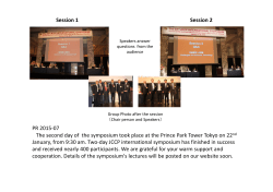


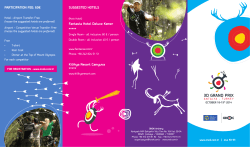
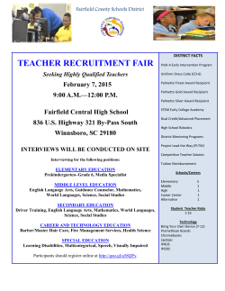


© Copyright 2026