
EN14 103 Engineering Physics
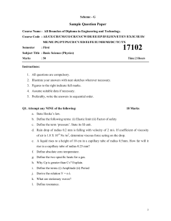
COMBINED FIRST AND SECOND SEMESTER B.TECH (ENGINEERING)
EXAMINATION; EN 14 103 – ENGINEERING PHYSICS
Time: 3 Hours
maximum marks: 100
PART A: Analytical/problem solving SHORT questions
Answer Eight questions out of Ten (Each Question carries 5 marks)
1. What is the difference between interference and diffraction?
2. What is Rayleigh’s criterion for resolving power? How to express resolving power of
a grating?
3. Define Brewster’s (polarizing) angle?
4. What is mean by double refraction?
5. What are the silent features of F.D. Statistics?
6. Define spontaneous emission and stimulated emission?
7. Define acceptance angle and numerical aperture?
8. What are the properties of nanomaterial?
9. Distinguish between intrinsic and extrinsic semiconductors?
10. Write short note on HTSC?
(8*5 =40marks)
PART B: Analytical/Problem solving DESCRIPTIVE questions
Answer all questions (Each Question carries 15 marks)
(15*4=60 marks)
11. i. Derive time dependent Schrodinger wave equation? ii. Explain the physical
significance
of
wave
function?
(OR)
12. i. Explain construction and working of Laurent’s half shade polarimeter? ii. Explain
the production and detection of elliptically & circularly polarized light?
13. i. Describe the laboratory experiment to determine the velocity of ultrasonic waves in
a
given
liquid
by
forming
an
acoustic
grating.
ii.What is the properties of ultrasonic waves.
(OR)
14. i. Discuss the theory of Newton’s Rings with relevant diagram and derive expression
for the wavelength of light using dark and bright rings.
15. i. Explain the principle, construction, working, advantages, disadvantages, and
applications of semiconductor laser? (OR)
16. i. derive the expression for N.A., in terms of n1(refractive index of core), and ∆
(fractional refractive index change) ii. Explain the construction and working of Ruby
laser.
17. i. explain type I and type II superconductors with suitable example. ii .write short
notes on LED & solar cell. (OR)
18. i. Derive expression for Fermi level in extrinsic semiconductors? ii. Explain the
construction and working of tunnel diode?
ANSWERS OF MODEL QUESTION PAPER
1.
2.
3.
4.
5.
6.
7.
8.
.
9.
10.
11.i.
ii.
12.i
13. i.
ii.
14.i.
15.i
16.i.
ii.
17.i.
ii.
18.i.
ii.


© Copyright 2026