
Telecommunications Demystified
LICENSE INFORMATION This is a single-user version of this eBook. It may not be copied or distributed. Unauthorized reproduction or distribution of this eBook may result in severe civil and criminal penalties. Telecommunications Demystified A Streamlined Course in Digital Communications (and some Analog) for EE Students and Practicing Engineers by Carl Nassar Eagle Rock, Virginia www.LLH-Publishing.com Copyright © 2001 by LLH Technology Publishing All rights reserved. No part of this book may be reproduced, in any form or means whatsoever, without written permission of the publisher. While every precaution has been taken in the preparation of this book, the publisher and author assume no responsibility for errors or omissions. Neither is any liability assumed for damages resulting from the use of information contained herein. Printed in the United States of America. ISBN 1-878707-77-9 (eBook) LLH Technology Publishing and HighText Publications are trademarks of Lewis Lewis & Helms LLC, 3578 Old Rail Road, Eagle Rock, VA, 24085 Contents Click the page number to go to that page. Foreword xv What’s on the CD-ROM? xvii CHAPTER 1 Introducing Telecommunications ........................................................ 1 1.1 Communication Systems ................................................................... 1 1.1.1 Definition ................................................................................... 1 1.1.2 The Parts of a Communication System ................................. 2 1.1.3 An Example of a Communication System ............................. 2 1.2 Telecommunication Systems ............................................................. 3 1.2.1 Definition ................................................................................... 3 1.2.2 Four Examples and an Erratic History Lesson .................... 4 1.3 Analog and Digital Communication Systems .................................. 6 1.3.1 Some Introductory Definitions ............................................... 6 1.3.2 Definitions ................................................................................. 7 1.3.3 And Digital Became the Favorite ........................................... 8 1.3.4 Making It Digital ...................................................................... 9 1.4 Congrats and Conclusions ............................................................... 10 CHAPTER 2 Telecommunication Networks .......................................................... 13 2.1 Telecommunication Network Basics .............................................. 13 2.1.1 Connecting People with Telephones .................................... 13 2.1.2 Connecting More People, Farther Apart ............................. 14 2.1.3 Multiplexing—An Alternative to a Lot of Wire ................... 16 iii Telecommunications Demystified 2.2 POTS: Plain Old Telephone System ............................................... 19 2.2.1 Local Calls ............................................................................... 19 2.2.2 Long Distance Calls ............................................................... 20 2.2.3 The Signals Sent from Switching Center to Switching Center ................................................................... 21 2.3 Communication Channels................................................................ 24 2.3.1 Transmission Lines (Wires) ................................................. 24 2.3.2 Terrestrial Microwave ........................................................... 26 2.3.3 Satellite Connections .............................................................. 28 2.3.4 Fiber-optic Links ..................................................................... 29 2.4 Data Communication Networks ...................................................... 31 2.5 Mobile Communications .................................................................. 33 2.6 Local Area Networks (LANs) .......................................................... 35 2.7 Conclusion ......................................................................................... 37 CHAPTER 3 A Review of Some Important Math, Stats, and Systems ....................... 39 3.1 Random Variables ............................................................................. 39 3.1.1 Definitions ................................................................................ 39 3.1.2 The Distribution Function: One Way to Describe x ........... 39 3.1.3 The Density Function: A Second Way to Describe x .......... 40 3.1.4 The Mean and the Variance .................................................. 41 3.1.5 Multiple Random Variables ................................................... 44 3.2 Random Processes ........................................................................... 45 3.2.1 A Definition ............................................................................. 45 3.2.2 Expressing Yourself, or a Complete Statistical Description .. 47 3.2.3 Expressing Some of Yourself, or a Partial Description ...... 47 3.2.4 And in Telecommunications … ............................................. 48 3.3 Signals and Systems: A Quick Peek ............................................... 50 3.3.1 A Few Signals .......................................................................... 50 3.3.2 Another Way to Represent a Signal: The Fourier Transform .......................................................... 51 3.3.3 Bandwidth ............................................................................... 53 3.3.4 A Linear Time Invariant (LTI) System ................................ 55 3.3.5 Some Special Linear Time Invariant (LTI) Systems .......... 56 3.4 Onward ............................................................................................... 58 iv Telecommunications Demystified CHAPTER 4 Source Coding and Decoding: Making it Digital ................................. 61 4.1 Sampling ............................................................................................ 61 4.1.1 Ideal Sampling ........................................................................ 61 4.1.2 Zero-order Hold Sampling ..................................................... 67 4.1.3 Natural Sampling .................................................................... 69 4.2 Quantization ...................................................................................... 71 4.2.1 Meet the Quantizer ................................................................ 71 4.2.2 The Good Quantizer ............................................................... 77 4.2.3 The Quantizer and the Telephone ........................................ 88 4.3 Source Coding: Pulse Code Modulator (PCM) ............................. 92 4.3.1 Introducing the PCM ............................................................. 92 4.3.2 PCM Talk ................................................................................ 93 4.3.3 The “Good” PCM.................................................................... 94 4.3.4 Source Decoder: PCM Decoder ........................................... 95 4.4 Predictive Coding ............................................................................. 96 4.4.1 The Idea Behind Predictive Coding ..................................... 97 4.4.2 Why? ........................................................................................ 97 4.4.3 The Predicted Value and the Predictive Decoder ............... 98 4.4.4 The Delta Modulator (DM) ................................................... 99 4.4.5 The Signals in the DM ......................................................... 101 4.4.6 Overload and Granular Noise ............................................. 105 4.4.7 Differential PCM (DPCM) .................................................. 107 4.5 Congrats and Conclusion ............................................................... 110 CHAPTER 5 Getting It from Here to There: Modulators and Demodulators .......... 115 5.1 An Introduction ............................................................................... 115 5.2 Modulators ...................................................................................... 116 5.2.1 Baseband Modulators .......................................................... 116 5.2.2 Bandpass Modulators .......................................................... 124 5.3 Just-in-Time Math, or How to Make a Modulator Signal Look Funny ..................................................................................... 133 5.3.1 The Idea ................................................................................. 134 5.3.2 Representing Modulated Signals ........................................ 138 v 5.4 Bring it Home, Baby, or Demodulators ........................................ 146 5.4.1 What Demodulators Do ........................................................ 146 5.4.2 The Channel and Its Noise .................................................. 147 5.4.3 Building a Demodulator, Part I—the Receiver Front End.......................................... 148 5.4.4 The Rest of the Demodulator, Part II—The Decision Makers ........................................... 152 5.4.5 How to Build It ...................................................................... 156 5.5 How Good Is It Anyway (Performance Measures) .................... 161 5.5.1 A Performance Measure ..................................................... 161 5.5.2 Evaluation of P(ε ) for Simple Cases ................................. 162 5.5.3 Some well-known P(ε ) ’s ..................................................... 166 5.6 What We Just Did ........................................................................... 166 CHAPTER 6 Channel Coding and Decoding: Part 1–Block Coding and Decoding ... 171 6.1 Simple Block Coding ..................................................................... 172 6.1.1 The Single Parity Check Bit Coder .................................... 172 6.1.2 Some Terminology ............................................................... 175 6.1.3 Rectangular Codes ............................................................... 175 6.2 Linear block codes .......................................................................... 177 6.2.1 Introduction ........................................................................... 177 6.2.2 Understanding Why ............................................................. 179 6.2.3 Systematic Linear Block Codes .......................................... 181 6.2.4 The Decoding ....................................................................... 182 6.3 Performance of the Block Coders ................................................ 188 6.3.1 Performances of Single Parity Check Bit Coders/Decoders ................................................................ 188 6.3.2 The Performance of Rectangular Codes............................ 189 6.3.3 The Performance of Linear Block Codes .......................... 189 6.4 Benefits and Costs of Block Coders ............................................. 192 6.5 Conclusion ....................................................................................... 193 vi CHAPTER 7 Channel Coding and Decoding: Part 2–Convolutional Coding and Decoding .................................... 197 7.1 Convolutional Coders ..................................................................... 197 7.1.1 Our Example ......................................................................... 197 7.1.2 Making Sure We’ve Got It ................................................... 199 7.1.3 Polynomial Representation .................................................. 200 7.1.4 The Trellis Diagram ............................................................. 201 7.2 Channel Decoding .......................................................................... 203 7.2.1 Using a Trellis Diagram ...................................................... 204 7.2.2 The Viterbi Algorithm ........................................................... 206 7.3 Performance of the Convolutional Coder .................................... 213 7.4 Catastrophic Codes ........................................................................ 214 7.5 Building Your Own ......................................................................... 216 CHAPTER 8 Trellis-Coded Modulation (TCM) The Wisdom of Modulator and Coder Togetherness ......................... 221 8.1 The Idea ........................................................................................... 222 8.2 Improving on the Idea .................................................................... 225 8.3 The Receiver End of Things .......................................................... 230 8.3.1 The Input ............................................................................... 231 8.3.2 The TCM Decoder Front End ............................................ 233 8.3.3 The Rest of the TCM Decoder............................................ 234 8.3.4 Searching for the Best Path ................................................ 237 CHAPTER 9 Channel Filtering and Equalizers ................................................... 245 9.1 Modulators and Pulse Shaping ..................................................... 245 9.2 The Channel That Thought It Was a Filter ................................. 249 9.3 Receivers: A First Try .................................................................... 251 9.3.1 The Proposed Receiver ........................................................ 251 9.3.2 Making the Receiver a Good One ...................................... 254 9.3.3 The Proposed Receiver: Problems and Usefulness .......... 256 9.4 Optimal Receiver Front End .......................................................... 258 vii 9.5 Optimal Rest-of-the-Receiver ......................................................... 262 9.5.1 The Input ................................................................................ 262 9.5.2 A Problem with the Input, and a Solution .......................... 264 9.5.3 The Final Part of the Optimal Receiver ............................. 265 9.5.4 An Issue with Using the Whitening Filter and MLSE...... 271 9.6 Linear Equalizers ............................................................................ 271 9.6.1 Zero Forcing Linear Equalizer ............................................ 272 9.6.2 MMSE (Minimum Mean Squared Error) Equalizer ........ 273 9.7 Other Equalizers: the FSE and the DFE ...................................... 274 9.8 Conclusion ....................................................................................... 275 CHAPTER 10 Estimation and Synchronization ..................................................... 279 10.1 Introduction ................................................................................... 279 10.2 Estimation ...................................................................................... 280 10.2.1 Our Goal ............................................................................ 280 10.2.2 What We Need to Get an Estimate of a Given r ............ 281 10.2.3 Estimating a Given r, the First Way ................................ 281 10.2.4 Estimating a Given r, the Second Way ........................... 282 10.2.5 Estimating a Given r, the Third Way .............................. 283 10.3 Evaluating Channel Phase: A Practical Example ...................... 285 10.3.1 Our Example and Its Theoretically Computed Estimate .. 285 10.3.2 The Practical Estimator: the PLL ................................... 290 10.3.3 Updates to the Practical Estimator in MPSK ................ 292 10.4 Conclusion ..................................................................................... 294 CHAPTER 11 Multiple Access Schemes: Teaching Telecommunications Systems to Share ............................... 299 11.1 11.2 11.3 11.4 11.5 What It Is ....................................................................................... 299 The Underlying Ideas ................................................................... 300 TDMA ............................................................................................ 303 FDMA ............................................................................................ 305 CDMA ............................................................................................ 306 11.5.1 Introduction ....................................................................... 306 11.5.2 DS-CDMA .......................................................................... 310 viii 11.5.3 FH-CDMA ......................................................................... 312 11.5.4 MC-CDMA ........................................................................ 313 11.6 CIMA .............................................................................................. 315 11.7 Conclusion ..................................................................................... 318 CHAPTER 12 Analog Communications ............................................................... 321 12.1 Modulation—An Overview .......................................................... 321 12.2 Amplitude Modulation (AM) ....................................................... 322 12.2.1 AM Modulators—in Time ............................................... 323 12.2.2 AM Modulation—in Frequency ...................................... 326 12.2.3 Demodulation of AM Signals—Noise-Free Case .......... 328 12.2.4 An Alternative to AM—DSB-SC...................................... 330 12.3 Frequency Modulation (FM) ....................................................... 334 12.3.1 The Modulator in FM ...................................................... 335 12.3.2 The Demodulator in FM .................................................. 339 12.4 The Superheterodyne Receiver ................................................... 339 12.5 Summary ....................................................................................... 341 Annotated References and Bibliography ......................................... 345 Index .......................................................................................... 349 ix [This is a blank page.] Acknowledgments In this life of mine, I have been blessed with an abundance of wonderful people. This book would be incomplete without at least a page to say “thank you,” for these are people alive in me and, therefore, alive in the pages of this book. Dr. Reza Soleymani, your careful guidance through the turmoil that surrounded my Ph.D. days was nothing short of a miracle. You showed me, through your example, how to handle even the most difficult of situations with grace and grit, both academically and in all of life. Dr. Derek Lile, Department Head at CSU—a young faculty could not ask for better guidance. Your thoughtfulness, caring, and gentle support have helped nurture the best of who I am. I am grateful. Steve Shattil, Vice President of Idris Communications, you are indeed a genius of a man whose ideas have inspired me to walk down new roads in the wireless world. Arnold Alagar, President of Idris, thank you for sharing the bigger picture with me, helping guide my research out of obscure journals and into a world full of opportunity. To both of you, I am grateful for both our technological partnerships and our friendships. Bala Natarajan and Zhiqiang Wu, my two long-time Ph.D. students, your support for my research efforts, through your commitment and dedication, has not gone unnoticed. Thank you for giving so fully of yourselves. Dr. Maier Blostien, who asked me to change my acknowledgments page in my Ph.D. thesis to something less gushy, let me thank you now for saving the day when my Ph.D. days looked numbered. I appreciate your candor and your daring. Carol Lewis, my publisher at LLH Technology Publishing, thank you for believing in this project and moving it from manuscript to “masterpiece.” Gretchen Brooks Nassar, you hold my hand and invite me to fly off the cliffs and into Oceans of Wonder. Your support in inviting me to pursue my dreams is nothing short of a gift straight from the heavens. I love you. xi And to the three of you who have loved me my whole life, and given me the best of who you are, Mom (Mona), Dad (Rudy), and Christine (sister)—your love has shaped me and has made this book a possibility. Wow! And to all of you I haven’t mentioned, who appeared in my life and shared your light with me, thank you. xii About the Author Carl R. Nassar, Ph.D., is an engineering professor at Colorado State University, teaching telecommunications in his trademark entertaining style. He is also the director of the RAWCom (Research in Advanced Wireless Communications) Laboratory, where he and his graduate students carry out research to advance the art and science of wireless telecommunications. In addition, he is the founder of the Miracle Center, an organization fostering personal growth for individuals and corporations. Since Carl’s undergraduate and graduate school days at McGill University, he has dreamed of creating a plain-English engineering text with “personality.” This book is that dream realized. To contact the author, please write or e-mail him at Carl R. Nassar, Ph.D. Department of ECE Colorado State University Fort Collins, CO 80523-1373 [email protected] xiii [This is a blank page.] Foreword I first met the author of this book, Professor Carl Nassar, after he presented a paper at a conference on advanced radio technology. Professor Nassar’s presentation that day was particularly informative and his enthusiasm for the subject matter was evident. He seemed especially gifted in terms of his ability to explain complex concepts in a clear way that appealed to my intuition. Some time later, his editor asked me if I would be interested in reviewing a few chapters of this book and preparing a short preface. I agreed to do so because, in part, I was curious whether or not his accessible presentation style carried over into his writing. I was not disappointed. As you will soon see as you browse through these pages, Professor Nassar does have an uncanny ability to demystify the complexities of telecommunications systems engineering. He does so by first providing for an intuitive understanding of the subject at hand and then, building on that sound foundation, delving into the associated mathematical descriptions. I am partial to such an approach for at least two reasons. First, it has been my experience that engineers who combine a strong intuitive understanding of the technology with mathematical rigor are among the best in the field. Second, and more specific to the topic of this book, because of the increased importance of telecommunications to our economic and social well-being, we need to encourage students and practicing engineers to enter and maintain their skills in the field. Making the requisite technical knowledge accessible is an important step in that direction. In short, this book is an important and timely contribution to the telecommunications engineering field. Dale N. Hatfield Former Chief, Office of Engineering and Technology Federal Communications Commission xv [This is a blank page.] What’s on the CD-ROM? The CD-ROM accompanying this book contains a fully searchable, electronic version (eBook) of the entire contents of this book, in Adobe® pdf format. In addition, it contains interactive MATLAB® tutorials that demonstrate some of the concepts covered in the book. In order to run these tutorials from the CD-ROM, you must have MATLAB installed on your computer. MATLAB, published by The MathWorks, Inc., is a powerful mathematics software package used almost universally by the engineering departments of colleges and universities, and at many companies as well. A reasonably priced student version of MATLAB is available from www.mathworks.com. A link to their web site has been provided on the CD-ROM. Using the Tutorials Each tutorial delves deeper into a particular topic dealt with in the book, providing more visuals and interaction with the concepts presented. Note that the explanatory text box that overlays the visuals can be dragged to the side so that you can view the graphics and other aids before clicking “OK” to move to the next window. Each tutorial filename reflects the chapter in the book with which it is associated. I recommend that you read the chapter first, then run the associated tutorial(s) to help deepen your understanding. To run a particular tutorial, open MATLAB and choose Run Script from the Command Window File menu. When prompted, locate the desired tutorial on the CD-ROM using the Browse feature and click “OK.” The tutorials contain basic descriptions and text to help you use them. Brief descriptions are also given in the following pages. MATLAB is a registered trademark of The MathWorks, Inc. xvii ch2.m Demonstrates the creation of the DS-1 signal. ch4_1.m Shows the different sampling techniques, and the effects of sampling at above and below the Nyquist rate. ch4_2.m Demonstrates quantization, and computation of the MSE. ch4_3.m Explains the operation of the DM. ch5_1.m Shows the workings of modulation techniques such as BPSK and BFSK. ch5_2.m Explains how three signals are represented by two orthonormal basis functions. ch5_3.m Illustrates the damaging effect of noise and the operation of decision devices. ch5_4.m Demonstrates the performance curve for BPSK signals. ch7.m Shows how a convolutional coder and convolutional decoder work. xviii ch8.m Provides an example of how TCM works at the coder and the decoder side. ch9_1.m Demonstrates how the sinc and raised cosine pulse shapes avoid ISI. ch9_2.m Shows how the decision device operates in the optimal receiver. ch11.m Provides colorful examples of TDMA, FDMA, MC-CDMA, DS-CDMA, and CIMA. ch12.m Illustrates the different analog modulation techniques. Please note that the other files on the CD-ROM are subroutines that are called by the above-named files. You won’t want to run them on their own, but you will need them to run these tutorials. For MATLAB product information, please contact: The MathWorks, Inc. 3 Apple Hill Drive Natick, MA, 01760-2098 USA Tel: 508-647-7000 Fax: 508-647-7101 E-mail: [email protected] Web: www.mathworks.com xix [This is a blank page.] Chapter 1 Introducing Telecommunications I can still recall sitting in my first class on telecommunications as an undergrad—the teacher going off into a world of technical detail and I in my chair wondering, “What is this stuff called communications and telecommunications?” So, first, some simple definitions and examples—the big picture. 1.1 Communication Systems 1.1.1 Definition A communication system is, simply, any system in which information is transmitted from one physical location—let’s call it A—to a second physical location, which we’ll call B. I’ve shown this in Figure 1.1. A simple example of a communication system is one person talking to another person at lunch. Another simple example is one person talking to a second person over the telephone. Figure 1.1 A communication system 2 ◆ Chapter One 1.1.2 The Parts of a Communication System Any communication system is made up of three parts, shown in Figure 1.2. First is the transmitter, the part of the communication system that sits at point A. It includes two items: the source of the information, and the technology that sends the information out over the channel. Next is the channel. The channel is the medium (the stuff) that the information travels through in going from point A to point B. An example of a channel is copper wire, or the atmosphere. Finally, there’s the receiver, the part of the communication system that sits at point B and gets all the information that the transmitter sends over the channel. We’ll spend the rest of this book talking about these three parts and how they work. TRANSMITTER RECEIVER CHANNEL A B Figure 1.2 Parts of a communication system 1.1.3 An Example of a Communication System Now, let’s run through a simple but very important example of a communication system. We’ll consider the example of Gretchen talking to Carl about where to go for lunch, as shown in Figure 1.3. Channel (the air) Figure 1.3 Gretchen talking to Carl at lunch Windpipe Vocal cords Introducing Telecommunications ◆ 3 The Transmitter The transmitter, in this case, is made up of parts of Gretchen, namely her vocal cords, windpipe, and mouth. When Gretchen wants to talk, her brain tells her vocal cords (found in her windpipe) to vibrate at between 100 Hz and 10,000 Hz, depending on the sound she’s trying to make. (Isn’t it cool that, every time you talk, a part of you is shaking at between 100 and 10,000 times per second?) Once Gretchen’s vocal cords begin to vibrate, here are the three things that happen next: (1) the vibrations of her vocal cords cause vibrations in the air in her windpipe; (2) these vibrations in the air move up her windpipe to her mouth; and (3) as the vibrating air moves out through Gretchen’s mouth, the shape of her mouth and lips, and the position of her tongue, work together to create the intended sound. The Channel In our example, the channel is simply the air between Gretchen and Carl. The shaped vibrations that leave Gretchen’s mouth cause vibrations in the air, and these vibrations move through the air from Gretchen to Carl. The Receiver The receiver in this case is Carl’s eardrum and brain. The vibrations in the air hit Carl’s eardrum, causing it to vibrate in the same way. Carl’s shaking eardrum sends electrical signals to his brain, which interprets the shaking as spoken sound. The human eardrum can actually pick up vibrations between 50 Hz and 16,500 Hz, allowing us to hear sounds beyond the range of what we can speak, including a variety of musical sounds. 1.2 Telecommunication Systems 1.2.1 Definition A telecommunication system is two things: (1) a communication system—that is, a system in which information is transmitted from one physical location, A, to a second physical location, B; and (2) a system which allows this information to be sent beyond the range of usual vocal or visual communications. Gretchen and Carl’s lunchtime chat would not qualify as a telecommunication system, but the telephone system which they used later for an afternoon talk does qualify. 4 ◆ Chapter One 1.2.2 Four Examples and an Erratic History Lesson Here are four examples of telecommunication systems, ordered chronologically to create what we’ll optimistically call “a brief history of telecommunications.” Smoking Up In the B.C.’s, smoke signals were sent out using fire and some smoke signal equipment (such as a blanket). The smoke, carried upward by the air, was seen by people far (but not too far) away, who then interpreted this smoke to have some meaning. It is said that a fellow named Polybius (a Greek historian) came up with a system of alphabetical smoke signals in the 100s B.C., but there are no known recorded codes. Wild Horses Until the 1850s in the U.S., the fastest way to send a message from one’s home to someone else’s home was by Pony Express. Here, you wrote what you wanted to say (the transmitter), gave the writing to a Pony Express man, who then hopped on his horse and rode to the destination (the channel), where the message would be read by the intended person (the receiver). Telegraph In 1844, a fellow named Samuel Morse built a device he called the telegraph, the beginning of the end of the Pony Express. The transmitter consisted of a person and a sending key, which when pressed by the person, created a flow of electricity. This key had three states: “Off” which meant the key was not pressed; “Dot,” which meant the key was pressed for a short time and then released; and “Dash,” which meant the key was pressed for a longer time and then released. Each letter of the alphabet was represented by a particular sequence of dots and dashes. To keep the time to send a message short, the most commonly used letters in the alphabet were represented by the fewest possible dots or dashes; for example, the commonly used “t” was represented by a single dash, and the much- loved “e” was represented by a single dot. This system of representing letters is the well-known Morse code. The channel was an iron wire. The electricity created by the person and the sending key (the transmitter) was sent along this wire to the receiver, which consisted of an audiospeaker and a person. When the electricity entered the audio-speaker from the iron wire, it made a beeping sound. A “Dot” sounded like a short beep, and a “Dash” sounded like a longer beep. The person, upon hearing these beeps, would then decode the letters that had been sent. The overall system could send about two letters a second, or 120 letters a minute. The first words sent over the telegraph, by inventor Morse himself, were “What has God wrought!” (I have since wondered what Morse, who basically invented a simple dot-dash sending system, would have said about, oh, say, a nuclear bomb.) The Telephone The telephone was invented in 1876 by Alexander Graham Bell, whose first words on the phone were, “Mr. Watson, come at once, I need you.” Alex had just spilled battery acid down his pants and, as you can imagine, was in quite urgent need of his assistant’s help. Figure 1.4 shows an illustration of two people, who Introducing Telecommunications ◆ 5 we’ll call Carl and Monica, using the telephone. What follows is a wordy description of how the telephone works. Refer to Figure 1.4 to help you with the terms. The transmitter consists of Monica (who is talking) and the transmitting (bottom) end of the telephone. Monica speaks, and her vocal cords vibrate. This causes vibrations in the air, which travel through and out her mouth, and then travel to the bottom end of the telephone. Inside the bottom end of the telephone is a diaphragm. When the vibrations of the air arrive at this diaphragm, it, like an eardrum, begins to vibrate. Directly behind the diaphragm are a bunch of carbon granules. These granules are part of an electrical circuit, which consists of a 4-V source, copper wire, and the carbon granules. The carbon granules act as a resistor (with variable resistance) in the circuit. When the diaphragm is pushed back by the vibrating air, it causes the carbon granules (right behind it) to mush together. In this case, the granules act like a low-resistance resistor in the circuit. Hence, the current flowing though the electric circuit is high (using the well-known V = R ⋅ I rule). When the diaphragm is popped out by the vibrating air, it causes the carbon granules (right behind it) to separate out. In this case, those carbon granules are acting like a high-resistance resistor in the electrical circuit. Hence, the current flowing though the circuit is low. Overall, vibrations in the diaphragm (its “pushing back” and “popping out”) cause the same vibrations (frequencies) to appear in the current of the electrical circuit (via those carbon granules). The channel is a copper wire. The vibrating current generated by the transmitter is carried along this wire to the receiver. Channel (copper wire) eardrum electromagnet 4v power supply Windpipe Vocal cords carbon granules diaphragm Monica Carl TRANSMITTER RECEIVER Figure 1.4 Monica and Carl talking on a telephone 6 ◆ Chapter One The receiver consists of two parts: the receiving (top) part of the telephone, and Carl’s ear. The current, sent along the copper wire, arrives at the top end of the telephone. Inside this top end is a device called an electromagnet and right next to that is a diaphragm. The current, containing all of Monica’s talking frequencies, enters into the electromagnet. This electromagnet causes the diaphragm to vibrate with all of Monica’s talking frequencies. The vibrating diaphragm causes vibrations in the air, and these vibrations travel to Carl’s ear. His eardrum vibrates, and these vibrations cause electrical signals to be sent to his brain, which interprets this as Monica’s sound. 1.3 Analog and Digital Communication Systems The last part of this chapter is dedicated to explaining what is meant by analog and digital communication systems, and then explaining why digital communication systems are the way of the future. 1.3.1 Some Introductory Definitions An analog signal is a signal that can take on any amplitude and is well-defined at every time. Figure 1.5(a) shows an example of this. A discrete-time signal is a signal that can take on any amplitude but is defined only at a set of discrete times. Figure 1.5(b) shows an example. Finally, a digital signal is a signal whose amplitude can take on only a finite set of values, normally two, and is defined only at a discrete set of times. To help clarify, an example is shown in Figure 1.5(c). x(t) x(t) x(t) 1 t (a) T 2T 3T 4T (b) ... t 0 T 2T 3T 4T ... (c) Figure 1.5 (a) An analog signal; (b) a discrete time signal; and (c) a digital signal t Introducing Telecommunications ◆ 7 1.3.2 Definitions An analog communication system is a communication system where the information signal sent from point A to point B can only be described as an analog signal. An example of this is Monica speaking to Carl over the telephone, as described in Section 1.2.2. A digital communication system is a communication system where the information signal sent from A to B can be fully described as a digital signal. For example, consider Figure 1.6. Here, data is sent from one computer to another over a wire. The computer at point A is sending 0s or 1s to the computer at point B; a 0 is being represented by –5 V for a duration of time T and a 1 is being represented by a +5 V for the same duration T. As I show in that figure, that sent signal can be fully described using a digital signal. A B s(t) Signal sent is: +5v 0 t -5v Can be represented by: 1 0 t 1 0 1 0 Figure 1.6 A computer sending information to another computer 8 ◆ Chapter One 1.3.3 And Digital Became the Favorite Digital communication systems are becoming, and in many ways have already become, the communication system of choice among us telecommunication folks. Certainly, one of the reasons for this is the rapid availability and low cost of digital components. But this reason is far from the full story. To explain the full benefits of a digital communication system, we’ll use Figures 1.7 and 1.8 to help. Let’s first consider an analog communication system, using Figure 1.7. Let’s pretend the transmitter sends out the analog signal of Figure 1.7(a) from point A to point B. This signal travels across the channel, which adds some noise (an unwanted signal). The signal that arrives at the receiver now looks like Figure 1.7(b). Let’s now consider a digital communication system with the help of Figure 1.8. Let’s imagine that the transmitter sends out the signal of Figure 1.8(a). This signal travels across the channel, which adds a noise. The signal that arrives at the receiver is found in Figure 1.8 (b). s(t) r(t) Noise t t (b) (a) Figure 1.7 (a) Transmitted analog signal; (b) Received analog signal Noise s(t) s(t) 1 1 0 +5v +5v 0 0 t -5v t -5v (a) (b) Figure 1.8 (a) Transmitted digital signal; (b) Received digital signal Introducing Telecommunications ◆ 9 Here’s the key idea. In the digital communication system, even after noise is added, a 1 (sent as +5 V) still looks like a 1 (+5 V), and a 0 (–5 V) still looks like a 0 (–5 V). So, the receiver can determine that the information transmitted was a 1 0 1. Since it can decide this, it’s as if the channel added no noise. In the analog communication system, the receiver is stuck with the noisy signal and there is no way it can recover exactly what was sent. (If you can think of a way, please do let me know.) So, in a digital communication system, the effects of channel noise can be much, much less than in an analog communication system. 1.3.4 Making It Digital A number of naturally occurring signals, such as Monica’s speech signal, are analog signals. We want to send these signals from one point, A, to another point, B. Because digital communication systems are so much better than analog ones, we want to use a digital system. To do this, the analog signal must be turned into a digital signal. The devices which turn analog signals into digital ones are called source coders, and we’ll spend all of Chapter 4 exploring them. In this section, we’ll just take a brief peek at a simple source coder, one that will turn Monica’s speech signal (and anyone else’s for that matter) into a digital signal. The source coder is shown in Figure 1.9. It all begins when Monica talks into the telephone, and her vibrations are turned into an electrical signal by the bottom end of the telephone talked about earlier. This electrical signal is the input signal in Figure 1.9. We will assume, as the telephone company does, that all of Monica’s speech lies in the frequency range of 100 Hz to 4000 Hz. The electrical version of Monica’s speech signal enters a device called a sampler. The sampler is, in essence, a switch which closes for a brief period of time and then opens, closing and opening many times a second. When the switch is closed, the electrical speech signal passes through; when the switch is open, nothing gets through. Hence, the output of the sampler consists of samples (pieces) of the electrical input. Monica's speech signal Quantizer Sampler Figure 1.9 A simple source coder Symbol-to-bit Mapper 10 ◆ Chapter One As some of you may know (and if you don’t, we’ll review it in Chapter 4, so have no worries), we want the switch to open and close at a rate of at least two times the maximum frequency of the input signal. In the case at hand, this means that we want the switch to open and close 2 × 4000 = 8000 times a second; in fancy words, we want a sampling rate of 8000 Hz. After the switch, the signal goes through a device called a quantizer. The quantizer does a simple thing. It makes the amplitude of each sample go to one of 256 possible levels. For example, the quantizer may be rounding each sample of the incoming signal to the nearest value in the set {0, 0.01, 0.02, ..., 2.54, 2.55}. Now, here’s something interesting. There is a loss of information at the quantizer. For example, in rounding a sample of amplitude 2.123 to the amplitude 2.12, information is lost. That information is gone forever. Why would we put in a device that intentionally lost information? Easy. Because that’s the only way we know to turn an analog signal into a digital one (and hence gain the benefits of a digital communication system). The good news here is engineers (like you and me) build the quantizer, and we can build it in a way that minimizes the loss introduced by the quantizer. (We’ll talk at length about that in Chapter 4.) After the quantizer, the signal enters into a symbol-to-bit mapper. This device maps each sample, whose amplitude takes on one of 256 levels, into a sequence of 8 bits. For example, 0.0 may be represented by 00000000, and 2.55 by 11111111. We’ve now created a digital signal from our starting analog signal. 1.4 Congrats and Conclusion Congratulations—you made it through the first chapter. Just to recap (and I’ll be brief), in this chapter we defined the words communication and telecommunication system. Next, I presented a whole gang of examples, to give you a feel for a few key communication and telecommunication systems. Finally, we talked about analog and digital communications, discovering that most telecommunication engineers dream in digital. Meet you in Chapter 2! Introducing Telecommunications Problems 1. Briefly describe the following: (a) telecommunication system (b) communication system (c) the difference between a communication system and a telecommunication system. (d) digital communications (e) analog communications (f) the main reason why digital communications is preferred (to analog communications). 2. Describe the function of the following: (a) source coder (b) quantizer (c) sampler (d) symbol-to-bit mapper. ◆ 11 [This is a blank page.] Chapter 2 Telecommunication Networks F irst, and always first, a definition. A telecommunication network is a telecommunication system that allows many users to share information. 2.1 Telecommunication Network Basics 2.1.1 Connecting People with Telephones Let’s say I have six people with telephones. I want to connect them together so they can speak to one another. One easy way to connect everyone is to put copper wires everywhere. By that, I mean use a copper wire to connect person 1 to person 2, a wire to connect person 1 to person 3, ..., a wire to connect person 1 to person 6, ..., and a wire to connect person 5 to person 6. I’ve shown this solution in Figure 2.1. But, ugh, all these wires! In general, I need N(N–1)/2 wires, where N is the number of people. So with only six people I need 15 wires, with 100 people I need 49,950 wires, and with a million people I need 499,999,500,000 wires. Too many wires. Let’s consider another way to connect users: put a switching center between the people, as shown in Figure 2.2. The early switchboards worked like this: Gretchen picks up her phone to call Carl. A connection is immediately made to Mavis, a sweet elderly operator seated at the switching center. Mavis asks Gretchen who she wants to talk to, and Gretchen says “Carl.” Mavis then physically moves wires at the switching center in such a way that the wire from Gretchen’s phone is directly connected to Carl’s wire, and Gretchen and Carl are now ready to begin their conversation. 2 3 Copper wire 1 4 6 5 Figure 2.1 A single wire between each phone 14 ◆ Chapter Two The manual switching center, operated by people like Mavis, was the only way 3 2 to go until a little after 1889 when Almon B. Strowger, a mortician by trade, invented the first automatic switching center. It seems that Almon suddenly found that he 1 Switching Center 4 was no longer getting any business. Surprised, he investigated and discovered that the new telephone operator was also married to the competition ... and she was switching all funeral home calls to her 6 5 husband. Determined to keep his mortician business alive (no pun intended), Almon created the first automatic switching center. Figure 2.2 These switching centers do not require Phones connected by a switching center anyone (and hence no competitor’s wife) to transfer calls. Entering a 7-digit phone number automatically sets up the connection at the switching center. Today, all switching centers are automatic. Just briefly, how many wires are needed by a network using a switching center? Only N, where N is the number of users. That’s far fewer than the many-wire system introduced first. 2.1.2 Connecting More People, Farther Apart Let’s take this switching center idea a bit further. Consider Figure 2.3. A bunch of people are connected together in Fort Collins, Colorado, by a switching center in downtown Fort Collins. Then, in nearby Boulder, another group of people are connected together by a second switching center. How does someone in Boulder talk to a friend in Fort Collins? One easy way is to simply connect the switching centers, as shown in Figure 2.3. If we put several wires between the Fort Collins and Boulder switching centers, then several people in Fort Collins can talk to people in Boulder at the same time. 3 2 1 1 4 4 Switching Center 6 3 2 Switching Center 6 5 Fort Collins, CO Figure 2.3 Connections between switching centers 5 Boulder, CO Telecommunication Networks ◆ 15 Consider now a number of other nearby cities, say Longmont and Denver. The folks in these towns want to talk to their friends in Boulder and Fort Collins. We could connect all the switching centers together, as shown in Figure 2.4. Alternatively, we could have a “super” switching center, which would be a switching center for the switching centers, as shown in Figure 2.5. 1 Boulder Fort Collins 1 2 2 3 3 Switching Center Switching Center 4 4 5 5 6 6 1 1 2 2 3 3 Switching Center Switching Center 4 4 5 5 6 Longmont Denver 6 Figure 2.4 Connecting all the switching centers together 1 Boulder Fort Collins 1 2 2 3 3 Switching Center Switching Center 4 4 5 "Super" Switching Center 5 6 1 2 6 1 2 3 3 Switching Center Switching Center 4 4 5 5 6 Longmont Denver 6 Figure 2.5 Connecting switching centers using a “super” switching center 16 ◆ Chapter Two 2.1.3 Multiplexing—An Alternative to a Lot of Wire Let’s go back to the Fort Collins and Boulder people in Figure 2.3. Let’s say we’ve connected their switching centers so they can talk to each other. As more people in Fort Collins want to talk to more people in Boulder, more and more wires need to be added between their switching centers. It could get to the point where there are far too many wires running between the switching centers. The skies around Fort Collins could grow dark under the cover of all these wires. This probably wouldn’t be true of a smaller town like Fort Collins, but it was true of big cities like New York. Finally, someone said, “Something must be done!’’ and multiplexing was invented. Multiplexing refers to any scheme that allows many people’s calls to share a single wire. (We’ll talk more about this in Chapter 11, but a brief introduction now is useful.) First There Was FDM FDM, short for frequency division multiplexing, was the first scheme created to allow people’s calls to share a wire. Let’s say Carl, Gretchen, and Monica all want to make a call from Fort Collins to Boulder. We only want to use one wire to connect calls between the two towns. This is shown in Figure 2.6. Carl’s speech, turned into a current on a wire, contains the frequencies 100 to 4000 Hz. His speech is left as is. Gretchen’s speech, turned into an electrical signal on a wire, also contains the frequencies 100 to 4000 Hz. A simple device called a mixer (operating at 8000 Hz) is applied to her speech signal. This device moves the frequency content of her speech signal, and the frequencies found at 100 Hz to 4,000 Hz are moved to the frequencies 8,100 Hz to 12,000 Hz, as shown in Figure 2.7. Switching Center Fort Collins Carl, Gretchen and Monica's voices all on one wire Figure 2.6 People’s speech on one wire Switching Center Boulder Telecommunication Networks ◆ 17 Because Carl and Gretchen’s calls are now made up of different frequency components, they can be sent on a single wire without interfering with one another. This too is shown in Figure 2.7. We now want to add Monica’s speech signal, since she too is making a call from Fort Collins to Boulder. A mixer, this one operating at 16,000 Hz, is applied to her speech signal. This moves the frequency content of Monica’s speech to 16,100 Hz to 20,000 Hz, as shown in Figure 2.7. Because Monica’s speech signal is now at different frequencies than Carl and Gretchen’s speech signals, her signal can be added onto the same wire as Carl and Gretchen’s, without interfering. (Again, take a peek at Figure 2.7.) Over in Boulder, we’ve got a wire with Carl, Gretchen, and Monica’s speech on it, and we need to separate this into three signals. First, to get Carl’s signal, we use a device called a low-pass filter (LPF). The filter we use only allows the frequencies in 0 to 4000 Hz to pass through; all other frequency components are removed. So, in our example, this filter passes Carl’s speech, but stops Gretchen’s and Monica’s speech cold. This is shown in Figure 2.8. Carl's speech signal 100-4000 Hz one wire Gretchen's speech signal 100-4000 Hz Monica's speech signal 100-4000 Hz Mixer 8000 Hz + Mixer 16,000 Hz Figure 2.7 Putting three signals on one wire using FDM + 18 ◆ Chapter Two Next, we want to recover Gretchen’s speech signal. This is a two-part job. First, a bandpass filter (BPF) is applied, with start frequency 8,000 Hz and stop frequency 12,000 Hz. This filter allows only the frequencies between 8,000 Hz and 12,000 Hz to pass through, cutting out every other frequency. In the case at hand, this means that only Gretchen’s speech signal gets through the filter. This is shown in Figure 2.8. We still have one task left. Gretchen’s speech signal has been moved from 100–4,000 Hz to 8,100–12,000 Hz. We want to bring it back to the original 100–4000 Hz. This is done by applying a mixer (operating at 8,000 Hz), which returns Gretchen’s voice signal to its original frequency components. Monica’s signal is recovered on a single wire in much the same way as Gretchen’s, and, rather than use many words, I’ll simply refer you to Figure 2.8. Figure 2.8 Getting three speech signals back from one wire in FDM Carl's speech signal LPF 0-4000 Hz Carl, Gretchen and Monica's speech on one wire BPF 8000-12000 Hz Mixer 8000 Hz BPF 16000-20000 Hz Mixer 16000 Hz Gretchen's speech signal Monica's speech signal Along Came TDM TDM, short for time-division multiplexing, is the second commonly used technique to let several people’s speech share a single wire. TDM works like this. Let’s say we’ve again got Carl, Gretchen, and Monica, who all want to make their calls from Fort Collins to Boulder. Carl, Gretchen, and Monica’s speech sounds are first turned into an electrical signal on a wire by their phones, as explained in Chapter 1. Then, their electrical speech signals are turned into digital signals, again as explained in Chapter 1. The digitized, electricized versions of the speech signal are the incoming signals that will share a wire. Figure 2.9 shows these incoming signals. These signals, coming along the wire, then meet “the big switch,” as shown in Figure 2.9. The big switch makes contact with each of the three incoming signals, touching each signal for T/3 seconds in every T-second interval. The output of this switch, again shown in Figure 2.9, consists of one piece of Carl’s speech, then one piece of Gretchen’s speech, then one piece of Monica’s speech in every T-second interval. In this way, a part of everybody’s speech sample gets onto one wire. These speech samples are now sharing time on the wire, and hence the name time-division multiplexing. Telecommunication Networks ... Carl's digital speech ◆ 19 t T ... Gretchen's digital speech T t Carl, Gretchen & Monica's digital speech "The Big Switch" Gretchen Monica Carl ... ... Monica's digital speech t T t T/3 T Figure 2.9 How three signals share one wire in TDM 2.2 POTS: Plain Old Telephone System Enough of the basics. Let me now introduce you to a telecommunication network currently in use. In fact, it’s the most frequently used telecommunication network in the world. It’s called POTS, short for Plain Old Telephone System. We’ll be considering the phone connections exclusively in Canada and the United States, but keep in mind that similar systems exist worldwide. 2.2.1 Local Calls Gretchen at home Carl at the office Let’s say Gretchen, at home in Fort Collins, decides to call Carl, who is hard at work at CSU writing this book. Here’s how the call gets from Gretchen to Carl. First, Gretchen’s phone turns her sounds into an analog electrical signal, as explained in Section 1.2.2. This analog electrical signal is sent along a Class 5 copper wire (called a twisted-pair cable) to the Switching Center (end office) switching center called the Class 5 switching center, or end office (Figure 2.10). Figure 2.10 Connecting a local call: the local loop 20 ◆ Chapter Two The switching center knows Gretchen’s call is a local call to Carl’s office (based on a 7-digit number she initially dialed), and it sends Gretchen’s speech signal down the copper wire that connects to Carl’s office. This signal then enters Carl’s phone, which turns the electrical signal back into Gretchen’s speech sounds, and there we have it. This part of the phone system is called the local loop. There are about 20,000 end offices in Canada and the United States. 2.2.2 Long Distance Calls Connecting the Call Let’s say that Carl’s mom, Mona, who lives in the cold of Montreal, Canada, wants to call Carl in Colorado and see if he’s eating well (yes, Mom, I’m eating well). How would the telephone system connect this call? We’ll use Figure 2.11 as our guide. First, Mona’s Are you eating well? sounds are turned into an analog electrical signal by her telephone. This electrical signal is sent along copper wire to the end office (or class 5 switching center). The end office, realizing that this isn’t a local call, does two things: (1) it mixes Mona’s signal with other people’s voice signals (that are also not local calls), using multiplexing; then, (2) it takes the mix of Mona’s speech signal and the other people’s speech signals and sends this mix to a bigger switching center, called a Class 4 switching center, or toll center, shown in Figure 2.11. The toll center is connected to three sets of things. A Class 5 End Office Multiplexing of Mona's speech and other speech AA Class 4 Toll Center Class 3 Primary Center Class 2 Class 1 B Class 5 End Office Class 1 C Class 5 End Office D Class 5 End Office Class 2 Class 4 Toll Center E Class 4 Toll Center Class 5 End Office Class 4 Toll Center Class 4 Toll Center F Class 5 End Office Class 2 BB Class 4 Toll Center Class 2 Class 3 Primary Center Class 3 Primary Center Class 3 Primary Center Figure 2.11 A long-distance call in POTS Telecommunication Networks ◆ 21 First, it’s connected to a number of end offices (A, B, C, and D in Figure 2.11), each end office like the one that Mona’s call came from. If Mona’s call was intended for a phone that was connected to end office C for example, then Mona’s speech would be sent to end office C and from there to the intended phone. The second thing the Class 4 switching center (toll center) is connected to is other Class 4 switching centers (BB in Figure 2.11). If the call is intended for a phone connected to end office E, then it would likely be sent to toll center BB, then to end office E, and then to the intended telephone. The third thing a Class 4 switching center is connected to is an even bigger switching center, which is called (no big surprise) a Class 3 switching center (also called a primary center). If Mona’s call is going to a phone not connected to any of the end offices available from toll centers AA or BB, then Mona’s speech moves along to the class 3 switching center. The good news is that the Class 3 switching center works in pretty much the same way as the Class 4 switching center. Basically, from the Class 3 switching center, Mona’s call can go to: (1) any Class 3, 4, or 5 switching center that is connected to the Class 3 switching center holding Mona’s speech—it will go that route if the intended phone is connected to one of these Class 3, 4, or 5 switching centers; otherwise, (2) the call will be switched to an even bigger switching center, called the Class 2 switching center (and also called the sectional center). Let’s say Mona’s call heads out to the Class 2 switching center. From here it gets to Carl in one of two ways: (1) if Carl’s phone is connected to a Class 2, 3, 4, or 5 switching center that is directly connected to the Class 2 switching center containing Mona’s voice, then Mona’s voice gets sent to that switching center; otherwise, (2) Mona’s call will go to the last, biggest switching center, the Class 1 switching center (or regional center). The Class 1 switching center will then send the call to either a Class 1, 2, 3, 4, or 5 switching center that it’s connected to, depending on which center is most directly connected to Carl’s phone. And that, my friends, is how Mona’s concern about Carl’s eating habits gets from Mona in Montreal to Carl in Colorado. It’s a 5-level hierarchy of switching centers. There are some 13,000 toll centers, 265 primary centers, 75 sectional centers, and 12 regional centers. 2.2.3 The Signals Sent from Switching Center to Switching Center We now understand that POTS is made up of five stages of switching centers. We understand how a person’s speech gets from one place to another using the phone system. Before we move on, I want to discuss what signals are sent from one switching center to another. 22 ◆ Chapter Two A telephone call starts out with the phone in your hand. That call goes to a Class 5 switching center. If the call is local, it goes from that Class 5 switching center right to the person you’re talking to. If the call is not local, the Class 5 switching center puts the call together with other long-distance calls, and sends them together to a Class 4 switching center. Let’s look at the signal created at a Class 5 switching center that is sent to a Class 4 switching center. Class 5 to Class 4 The Class 5 switching center gets the call you place. It also gets a lot of other calls from your neighborhood. When the Class 5 switching center realizes there are a bunch of calls that are not in its area (and instead are long-distance calls), it puts these signals together and sends them out. Specifically, it puts the signals together as shown in Figure 2.12: Class 5 Switching Center A A Your call #1 t T=1/8000=0.125ms 8000 samples/sec The Big Switch #2 * Symbol to bit mapper Quantizer Add 1 bit To class 4 #3 . . . . . . Forces each amplitude to the nearest one out of 256 permitted output amplitudes #24 * Piece from line #2 A Piece from line #24 . . . Piece from line #1 t T/24 T = 0.125ms Figure 2.12 The signal created at a Class 5 switching center (headed to Class 4) Telecommunication Networks ◆ 23 1. First, at the line marked #1, is your call. But that is only one thing coming into the Class 5 switching center. The center takes your call and at the same time takes 23 others, for a total of 24 calls. Those calls incoming to the Class 5 switching center are the lines marked #1 to #24. 2. The switching center puts these 24 calls on a single line using TDM. That idea is explained in Section 2.1.3, but here are some more details explaining exactly what the Class 5 switching center does. 2a. Each voice call is sampled. Specifically, samples of each voice call are taken at a rate of 8000 samples/second (i.e., at 8000 Hz). That means that each sample taken from a voice call lasts a total time of T = 1/8000 = 0.125 ms. 2b. Each sampled voice signal meets “the big switch.” The big switch makes contact with each digital voice signal briefly once every 0.125 ms. As a result, the signal that ends up on the wire following “the big switch” is a collection of all 24 voice signals. This is shown in Figure 2.12 better than my words can explain. 2c. On the wire following the big switch, we have all 24 voice samples smooshed together in the time T = 0.125 ms. The number of samples in each second is now 24 × 8,000 samples/second = 192,000 samples/second. 3. The 192,000 samples/second on our wire now enter through a device called a quantizer. The quantizer simply changes the amplitude of the incoming samples. Each incoming sample, which has some amplitude A, is mapped to an outgoing sample whose amplitude is one of 256 possible values. 4. Each sample, with an amplitude that is now one of 256 levels, can be fully represented by a set of 8 bits. (This is because with 8 bits we can represent all integers between 1 and 256.) A device called a symbol-to-bit mapper takes each sample with one of 256 possible amplitudes, and represents it with 8 bits. While before we had 24 samples in each 0.125 ms, we now have 24 × 8 = 192 bits in each 0.125 ms. 5. To tell people where each set of 192 bits begins and ends, an extra bit (a 0) is squeezed in so that we now have 193 bits in each 0.125 ms. That means we have a bit rate of 193 bits/0.125 ms = 1.544 Mb/s. These bits, with a bit rate of 1.544 Mb/s, are sent from the Class 5 switching center to the Class 4 switching center. The signal sent between the Class 5 and Class 4 switching centers is named DS-1. The wire which connects the Class 5 to the Class 4 switching center is called a trunk line, specifically a T-1 trunk line. 24 ◆ Chapter Two Other Signals between Switching Centers Figure 2.13 shows the different signals sent between different switching centers. Coming into a Class 4 center is a DS-1 signal. It is likely that this incoming signal will need to be sent to the Class 3 center. If that’s the case, the Class 4 center creates a very special signal for transmission up to Class 3. Specifically, it takes four DS-1 signals that are coming into it (from Class 5 centers) and puts these signals together onto a single wire using TDM. It adds a few extra bits to help the Class 3 center identify the beginning of what it gets and the end of it. When it’s all said and done, the signal that moves from Class 4 to Class 3 is a stream of bits with a bit rate of 6.312 Mb/s. That signal is called a DS-2 signal. A signal enters into a Class 3 switching center. This signal might need to move up to a Class 2 switching center. In that case, the Class 3 switching center puts together a special signal just for Class 2. It takes seven DS-2 signals that are coming into it (from Class 4 centers), and puts them together on a single wire using TDM. It adds a few extra bits to help the Class 2 office identify places where bit streams begin and end. Ultimately, it sends a signal to Class 2 that is a stream of bits with a bit rate of 44.736 Mb/s. This signal is called a DS-3 signal. Finally, it is possible in POTS that a signal arriving at a Class 2 switching center might be sent up to a Class 1 switching center. If that’s the case, Class 2 puts together a special signal for Class 1. Specifically, a Class 2 center takes five of the DS-3 signals that come into it (from Class 3 centers), and packages them together on a single wire using TDM. Including a few extra bits to make the package look nice for Class 1, the stream of bits sent to Class 1 has a bit rate of 274.1746 Mb/s. This signal is called DS-4. What I’ve said so far is true, but not the complete truth. In general, it is possible in POTS that DS-1, DS-2, DS-3, and DS-4 signals could be found between any two switching centers. For example, I presented DS-3 as the signal Class 3 sends to Class 2 switching centers. It is also possible in POTS that Class 3 sends a DS-2 signal to Class 2. 2.3 Communication Channels So far in our discussion, communication signals have been sent on wires. However, there are a number of different ways in which a communication signal can be sent from one point to another. Using a wire is just one way—POTS likes and embraces this way. In this section, I’ll outline the different ways you can send a signal from one point to another—that is, I’ll outline different communication channels. 2.3.1 Transmission Lines (Wires) There are two types of transmission lines (wires) over which communication signals are commonly sent. These are twisted-pair cable and coaxial cable. Telecommunication Networks ◆ 25 Class 4 Switching Center Class 5 S.C. DS-1 Class 5 S.C. DS-1 extra bits added Class 5 S.C. DS-1 ...to class 3 DS-2 Class 5 S.C. DS-1 (a) Class 3 Switching Center Class 4 S.C. Class 4 S.C. extra bits added Class 4 S.C. Class 4 S.C. ...to class 2 DS-3 . . . (b) Class 2 Switching Center Class 3 S.C. Class 3 S.C. Class 3 S.C. extra bits added Class 3 S.C. ...to class 1 DS-4 Class 3 S.C. (c) Figure 2.13 (a) Creation of DS-2 signal, (b) Creation of DS-3 signal, (c) Creation of DS-4 signal 26 ◆ Chapter Two In twisted-pair cable, a signal is sent from one point to another as a current along a wire. Signals that are sent in the frequency range of 0 to 1 MHz can be supported. The most common use for twisted-pair cables is in POTS. It forms most of the local loop connections. Specifically, in POTS, an insulated twisted-pair cable leaves from a home and is combined with many other twisted-pair cables from neighboring homes. You end up with one, big fat set of twisted-pair cables sent to the end office (Class 5). Coaxial cables are the second type of “wire” used to send communication signals. In coaxial cables, the communication information is sent as a current along a wire. Coaxial cables can support signals in the 100 kHz to 400 MHz range (a much larger range of frequencies than the twisted-pair cable can support). Perhaps the most common use of coaxial cable is in connections from TV cable providers to your home. Other uses include long-distance lines in POTS and local area networks (LANs), discussed a little later in this chapter. 2.3.2 Terrestrial Microwave Another way in which information can be sent from one point to another is by use of (1) a modulator, which turns the incoming information signal into a high-frequency electrical signal on a wire; and (2) an antenna, which turns the high-frequency signal into an electromagnetic wave sent through the atmosphere. At the receiver side, you use (1) a receiver antenna, which picks up the incoming electromagnetic wave and turns it back into the high-frequency electrical signal, and (2) a demodulator, which returns the high-frequency electrical signal back to the original information signals. Some examples of communication systems which send information in this way are radio stations, wireless communication systems (later in this chapter), and terrestrial microwave, which I’ll explain right now so you can get a better understanding of this idea. A terrestrial microwave transmitter is shown in Figure 2.14. I’ll explain its workings here in three points. 1. In Figure 2.14 you see the incoming information signal. In this example, the incoming information signal contains voice signals; specifically, it contains two DS-3 signals combined on a single wire using TDM methods. 2. The incoming information signal enters a modulator, and the modulator maps the incoming signal into a high-frequency electrical signal. For example, the modulator may map the incoming signal so that it is now centered around 3 GHz, 11 GHz, or 23 GHz. 3. The antenna takes the incoming electrical signal and maps it into an electromagnetic wave of frequency 3 GHz, 11 GHz, or 23 GHz (for example). These frequencies correspond to microwave frequencies on the EM (electromagnetic) spectrum, so the system is called a microwave system. Telecommunication Networks ◆ 27 Between the transmitter and receiver we place some devices called repeaters, shown in Figure 2.15. Repeaters are placed every 26 miles (40 kilometers). The repeater may do one of two things: (1) it may simply amplify and retransmit the signal at a higher power (non-regenerative repeater); or (2) it may receive the incoming signal, remove noise as best it can through a demodulation/remodulation process, and then retransmit the signal at a high power (regenerative repeater). We use repeaters for two reasons. First, because of the curvature of the earth, the transmit antenna will be hidden from the receiver if we do not place a repeater between the transmitter and receiver (Figure 2.15). Second, repeaters can be useful in reducing the impact of channel noise. Parabolic dish antenna r o lat du Mo ... High frequency signal (centered around 3 GHz, for example) EM wave Figure 2.14 Terrestrial microwave system transmitter 2 DS-3 signals 26 mi. i. 26 mi. 26 m Repeater #1 Repeater #2 Receiver Transmitter Figure 2.15 Repeaters 28 ◆ Chapter Two Finally, after travelling through the repeaters, the signal arrives at the receiver, shown in Figure 2.16. First, a receiver antenna is applied to return the signal to an electrical signal of a frequency of 3 GHz. Then, a demodulator is applied that returns the high-frequency signal to the original information signal. The terrestrial microwave system just Receiver described typically operates in frequency antenna High frequency ranges of 1 GHz to 50 GHz, and it has electrical signal been applied in a number of different communication systems. For Demodulator example, it has been used as a part of POTS, to connect two EM wave Information-bearing Class 2 switching centers signal separated by terrain such as swamp where it is very difficult Figure 2.16 Terrestrial microwave receiver to lay wire. This terrestrial microwave system has also been set up to connect large branches of big companies. It has also been implemented as a backup to fiber-optic links (later in this chapter). 2.3.3 Satellite Connections With satellite connections, a communication system is set up as shown in Figure 2.17. Here, a transmitter takes the incoming information signal, uses a modulator to turn it into a high-frequency signal, and then uses an antenna to turn the signal into an electromagnetic wave sent through the atmosphere (just as in terrestrial microwave). Figure 2.17 Satellite communication system Satellite Solar panels generating electricity to operate satellite 6 GHz Information signal 4 GHz Information signal r lato u Mod Dem o dula tor Ocean High-frequency electrical signal High-frequency electrical signal Telecommunication Networks ◆ 29 This signal is then sent up to a satellite in orbit around the earth. Specifically, the satellite is placed at 36,000 km (22,300 miles), and at that altitude it orbits the Earth at 6,870 mph. Moving at this speed, the satellite appears to be stationary when looked at from the equator, and so it is said to be in a geo-stationary orbit. The satellite picks up the signal and does two things: (1) it acts as a repeater; and (2) it shifts the frequency (for example, from 6 GHz to 4 GHz) and sends it back down to earth in the direction of the receiver. Modern satellites are being built which can do more signal processing at the satellite itself, but we won’t go into those details here. The signal leaves the satellite and heads back to the receiver on Earth. At that receiver, an antenna is applied that turns the incoming electromagnetic wave back to an electrical signal, and that electrical signal is returned to the original information signal by a device called a demodulator. Satellite communications operate in a number of frequency bands. Here are some of them: (1) C-band, which refers to 6-GHz uplink (“up” to the satellite) and 4-GHz downlink (“down” to the receiver); (2) Ku-band, which is 14-GHz uplink/12-GHz downlink; and (3) ACTS which refers to 30-GHz uplink/20-GHz downlink. Some of the many uses of satellite communications include satellite TV distribution, live TV transoceanic links, telephone communications over the oceans, backup to fiber-optic links, and GPS (Global Positioning System). GPS refers to a system of satellites which enables anyone, using a hand-held device, to determine their exact position on our planet (very useful for ships, backpackers, and companies with large fleets of trucks/cars/aircraft). 2.3.4 Fiber-optic Links Fiber-optic cable is a revolution in connecting transmitters to receivers. It seems possible to support incredible—and I do mean incredible—rates of information along this cable. Using fiber-optic cable, it appears that we can support 1014 bits/s, at the very least. Right now, we don’t know how to send information at this high a rate (although we’re moving in that direction)—we also don’t have that much information to send yet! In a fiber-optic cable system, you have an information signal, which is an incoming electrical signal. To use a fiber-optic cable, you have to turn this electrical signal into light. Figure 2.18 shows how you might do this at the transmitter side, using a device called an emitter. The emitter might be, for example, a LED (light-emitting diode) or an FP (Farby Parot) laser diode. 30 ◆ Chapter Two Incoming information on electrical signal Original information on electrical signal Cladding Core Detector Emitter Outgoing information on a light wave Light signal Figure 2.18 Fiber-optic link The fiber-optic cable, which you can also see in Figure 2.18, is made up of two parts: a core and a cladding. The light travels down the core. It remains in the core and never leaves it (never entering the cladding). This is because the two materials chosen for core and cladding are carefully selected to ensure that total internal refraction occurs—that means that as light enters the boundary between core and cladding, it is bent in such a way that it remains in the core. (For more on this, check out a physics book.) At the receiver side, the light signal, which has made it through the fiber-optic cable, must be returned to an electrical signal. That job is done using a detector, as seen in Figure 2.17. The detector might be, for example, a PIN diode or an APD (avalanche photo diode). The light sent down the fiber-optic cable corresponds to an electromagnetic wave with a frequency in the range of 1014 to 1015 Hz. As mentioned already, the system appears capable of sending information at rates of 1014 bits/s. Because of the incredible promise of fiber-optic cable, these cables are being placed everywhere. They have even been placed on the ocean floor between North America and Europe, competing with and in many cases replacing satellite links. Fiberoptic links are being used to connect switching centers in POTS. They are limiting the use of coaxial cable and twisted-pair cable to areas where they have already been put in place. Telecommunication Networks ◆ 31 2.4 Data Communication Networks We’ve seen POTS, and we’ve studied the different mediums through which a communication system can send its information. Let’s take some time here to explore some of the different ways and networks (other than POTS) which are in place to help people communicate with one another. We’ll start with a discussion of data communication. So far, in all the examples we’ve considered, we’ve discussed voice communication between different locations. But now we’ll talk about the transmission of data, which here we’ll define to be computer communication (that is, communication between computers). One of the most common ways in which people’s computers communicate is through the use of a modem and POTS (plain old telephone system), shown in Figure 2.19. Here we see a computer ready to send data on the far left. The data it wants to communicate is sent to a device called a modem, which is short for modulator/ demodular. The modem next to the computer on the left (sending computer) acts like a modulator, which means that it turns the digital signal (data) into a waveform ready for transmission over the telephone—specifically, it turns the data into a waveform that looks like a speech signal as far as the telephone is concerned (but it sure doesn’t sound like one). Then, the modem is connected to the twisted-pair cable that leaves the house. The data signal enters into the five-layer telephone system POTS, and travels through this system of wires and switching centers until it arrives at the receiver’s home. There, the signal travels into the home along a twisted-pair cable and enters into the modem. The modem in this case acts as a demodulator, and it turns the signal that looks like a speech signal (but doesn’t sound like one) back into the original data signal. That enters into the receiver, and in this way, the two computers can talk. Data to be sent (a digital signal) A signal which looks like a voice signal Modem Computer source acts like a modulator Through POTS, the telephone network Data sent Modem acts like a demodulator Computer sink Figure 2.19 Data communication via a modem and POTS Currently, because of the internet and the fact that people want data at higher and higher rates (higher rates than you can get using a modem), some alternatives to the modem are now being used. One involves using the coaxial cable that sends TV signals into your house to also send data to and from your computer. A second alternative is to use DSL (digital subscriber line). In this case, the data signal that your computer wants to send is combined with any telephone voice signals that are leaving the house (using FDM) and together these are sent out the telephone line to the Class 5 switching center. I won’t get into the details of either system here. 32 ◆ Chapter Two Beyond these ways of communicating data, which basically are all about updating existing voice/TV links so that they also carry computer data, there is another (a better) way. That way is based on using what is called a packet switched network. A packet switched network is a communication network designed specifically for the communication of data. The underlying idea behind the network is this. Data is very “bursty,” which means that data sent between computers is usually filled with times when lots of data is sent, followed by times when no data is sent, followed by times when lots of data is sent, and so on. As a result, people wanted to build a communication network that allowed for the connection between two computers to be turned “on” quickly when data was to be sent, and to be turned “off” when there was no data to be sent (so that the communication link could be used for other computer connections). Here is what engineers came up with. Figure 2.20 represents a packed switched communication network. Let’s say the computer marked “A” wants to send data to the computer marked “B.” What happens is this. 1. The data from A is broken down into small, equally sized packets of data. Each packet has on it the name of the computer it wants to go to (in our case computer B). 2. The first packet from computer A is sent out to the nearest node. The node, which represents a special processor, basically acts like a traffic policeman. It looks at the data and does two things. 2a. It checks to see if the packet has errors in it that occurred in transmission. If it sees too many errors, it is sent back; if has only a very few errors it is sent on. Computer A Figure 2.20 Data communication through a packet-switched network Data packet Data packet Node Node Node Node Computer B Telecommunication Networks ◆ 33 2b. If the packet is to be sent on, the node decides which is the best node to send it to, based on its final destination. 3. This movement from node to node continues until the data packet arrives at computer B. Each packet from computer A to computer B may follow a different path of nodes. And this, my readers, is how you build networks intended only for the transmission of data. 2.5 Mobile Communications One of the fastest growing markets in the world (and the one I am actively researching) is the field of wireless communications, also called mobile communications. People on the move (in their car, on their yacht, walking through busy downtown streets) believe that they must be able to reach other people through voice (and possibly data) communications. These people want anytime/anywhere/with-anyone communications, and they are willing to spend their hard-earned dollars to have it. As a result, many engineers work hard to give this to them. Taking a look at Figure 2.21, we see the idea underlying a mobile communication system. We have a person in his car with a mobile phone, which is made up of three parts. When he talks into it: 1. the phone turns the voice signal into a digital signal using a device called a codec (coder/decoder); EM wave 875 MHz EM wave 825 MHz MO DE M M DE MO Base station CO DE C MTSO DE CO C High frequency signal Digital version of voice signal Electrical signal representing voice signal High frequency signal Digital version of voice signal Electrical version of voice signal Figure 2.21 Mobile communication system fundamentals 34 ◆ Chapter Two 2. the phone takes the digital signal it just created and turns it into a high-frequency signal (for example, centered at about 825 MHz) using a device called a modem (modulator/demodulator); 3. the high-frequency signal feeds an antenna, and that antenna turns the highfrequency electrical signal into an electromagnetic wave (of frequency 825 MHz). The electromagnetic wave then travels through the air and is picked up by an antenna on a tower called a base station. The antenna on the base station turns the signal into an electric signal. The base station, with help from a switching center called the MTSO (Mobile Telephone Switching Office), figures out where the call is going, and then resends the signal down to the receiving mobile phone at a different frequency (for example, at about 875 MHz). The receiving mobile phone has an antenna on it, and this antenna picks up the electromagnetic signal intended for the phone, and turns it into an electrical signal (with frequency 875 MHz). This high-frequency electrical signal is turned into a lowfrequency digital signal by the modem. Finally, the digital signal is returned to the original speech signal by the codec. This signal travels from phone to person’s ear— and there you have it, a mobile communication system. When engineers first built such a system, they had a problem. The government only gave them a small band of frequencies to use for their wireless communication systems (for example, 824 MHz–849 MHz and 869 MHz–894 MHz). The problem with that was that many people wanted to use the wireless communication systems but with the limited frequencies, the systems could only support a few users. Then, an engineer had an idea he called the cellular concept, and wireless telecommunications was changed forever. The cellular concept idea is shown in Figure 2.22. Cell A Cell B 1. You can see that the entire area is divided up into small, funnyshaped regions. Each region is called a cell (as in cells in the body). Each cell is typically between 1 mile to 12 miles long. Figure 2.22 Cellular concept Telecommunication Networks ◆ 35 2. Each cell has its own base station. Mobile phones in a cell communicate through the base station in its cell. 3. The transmit power of a mobile phone in a cell is kept low. Any transmissions in the cell A that travel in the direction of cell B are effectively zero by the time they get to cell B. 4. Cell A and B use the exact same frequencies. They can do this because they are separated in space by a distance that makes cell A’s transmissions unnoticeable in cell B (and vice-versa). In this way, phone companies were able to support a large number of wireless users. When I teach this in my class, there are two common questions. I’ll ask these questions here and then provide the answers. Q: What happens if you are in cell A and want to call someone in cell B? A: If you are making a call while in cell A, and the user you want to talk to is in cell B, then your call goes to the base station in cell A. It is sent from there to the MTSO (Mobile Telephone Switching Center); from there the call is sent to the base station in cell B, which sends it down to the intended listener in cell B. Q: What happens if, when driving in your car, you head out of one cell and into another? A: If you move out of one cell and into another, then the wireless communication system switches your call from communication with the base station in the old cell to communication with the base station in the new cell. 2.6 Local Area Networks (LANs) The final section of this chapter describes a type of communication system known as a local area network, or LAN for short. As the name suggests, this is a network intended to allow a number of different users (usually computers) located close to one another to communicate together. It might be used in an office building, or in a university setting, to allow people’s computers to talk to one another. Typically, LANs provide very high-bit-rate communications, enabling multiple users to communicate lots of information very quickly. Two types of LANs have become popular. The first is called Ethernet, and the second is known as Token ring. Ethernet is shown in Figure 2.23. Here, you see three computers connected together by a single coaxial cable. These users can communicate at 10 Mb/s (traditional speed) or 100 Mb/s (high speed). Let’s say that computer A wants to talk with computer B. Here’s what happens: 36 ◆ Chapter Two Computer B Computer A Looks Sees it is not for him. Data Data Looks Sees data is for him. Reads data. Data Figure 2.23 LAN using Ethernet 1. Computer A listens to the cable to see if there is a communication transmission. If there is no transmission, then computer A sends its information on the cable. If there is a transmission, then computer A waits until the transmission is done, and then it begins to send its signal. 2. When computer A first sends out its information, it checks to see if another computer has sent a transmission at the same time. If not, Computer A continues to send its data. If computer A and another computer were trying to send data at the same time, a “collision” is detected. Computer A stops its transmission, waits a random amount of time, and then tries to send it again. 3. When computer A is able to send information on the line (and no “collision” is detected), it sends out the name of the destination computer, Computer B. All the computers look at the data, to see if it is for them. 4. Computer B sees its name and reads the information. That is, briefly, all there is to Ethernet connections. The second type of communication system is called a Token ring network. The Token ring network is shown in Figure 2.24, and it operates as follows: 1. When there is no computer transmitting, the bits 1 1 1 1 1 1 1 1 are sent around the ring connecting the computers. These 8 bits are called the token. 2. When computer A wants to send information, it listens to the ring to make sure the token is on the ring. If it is, it inverts the last bit of the token (putting out 1 1 1 1 1 1 1 0) and then follows this with its information. Computer A makes sure that it puts the name of the intended computer in its information—for example, if the data is headed to computer B, computer A makes sure it puts “computer B” in its sent data. Telecommunication Networks ◆ 37 Computer A 1111111 Data Token 11111 110 Coaxial cable Figure 2.24 Token ring network Computer B 3. Every computer picks up the data sent by computer A, and reads the name to see if it is the intended addressee. If it is not, the computer puts the information back on the ring without reading it. If the data is intended for the computer, the computer reads the data, and then puts it back on the ring. 4. Eventually, the data gets back to the computer who sent it. This computer picks up its data, and puts the token 1 1 1 1 1 1 1 1 back on the ring. And that is how computers communicate using Token ring links. 2.7 Conclusion This chapter introduced you to the world of communication systems. From here on, we’ll focus on the details of how these systems work. For example, we will look into a cellular phone. We will describe how the codec (coder/decoder) works in Chapter 4. We will understand how the modem (modulator/demodulator) works in Chapter 5. We will introduce an important part of digital communication systems, called the channel coder/decoder, in Chapter 6. Basically, in what follows, we get into what is called the “physical layer”—how all the insides work. But first is Chapter 3, a review of the statistics and signals and systems details that you’ll want to make sure you know before forging ahead. 38 ◆ Chapter Two Problems 1. Briefly describe the following: (a) how to connect 1000 users to one another without directly connecting every user to every other one. (b) two ways to put 1000 users on a single wire. (c) the cellular concept. 2. Describe three communication systems that send their signal as an EM wave through the atmosphere. 3. On your own, find on the web or in the library a telecommunication system not described in this chapter (e.g., HDTV, the Internet) and provide a two-page overview, highlighting how the system works. Chapter 3 A Review of Some Important Math, Stats, and Systems M y intention in writing this chapter is to give a quick review of key mathematical, statistical, and engineering concepts which we’ll use in our study of telecommunications. I basically provide a brief review of random variables and random processes, and then talk in passing about the Fourier transform and linear time invariant (LTI) systems. If this material is new to you, read what follows carefully and use the references to fill in any blanks you find; if this stuff is old hat, then give it a passing glance, if for no other reason than to familiarize yourself with the notation found throughout the book. 3.1 Random Variables First, I’ll briefly review random variables, limiting my discussion to continuous random variables. 3.1.1 Definitions First, as usual, some definitions. A random event, A, refers simply to an event with an unknown outcome. An example of a random event is tomorrow’s weather. Next, a random variable, x, is a number whose value is determined by a random event, A. For example, it may be tomorrow’s outdoor temperature in Fort Collins, Colorado (where I live). 3.1.2 The Distribution Function: One Way to Describe x Let’s say you’ve got a random variable, x, which is tomorrow’s temperature. You want to somehow be able to describe x = (tomorrow’s temperature) to someone. You don’t know exactly what this value will be, but you do know it’s the middle of summer, so you know it’s a lot more likely to be 80 degrees (Fahrenheit) than it is to be 0 degrees. This section is all about how you can describe a random variable, like tomorrow’s temperature, to someone without using a lot of words. 40 ◆ Chapter Three One way to fully characterize our random variable x is by a function called the probability distribution function, Fx ( X ) . The function Fx ( X ) is defined in words as follows: Fx ( X ) is the likelihood that the random variable x is less than the number X. In a nice, neat equation, Fx ( X ) is defined as Fx (X ) = P(x < X ) (3.1) where P( __ ) is shorthand for the words “probability that __ happens.” Let me clarify the meaning of Fx ( X ) by an example. Let’s again go back to x being tomorrow’s temperature, and let’s say it’s the middle of summer. Then: (1) Fx (0) = P(x<0) = (the probability that the temperature is less than 0), and this may be 1/1000000 (1 in a million), and (2) Fx (70) = P(x<70) = (the probability that the temperature is less than 70), and this may be ½ (1 in 2). By providing Fx ( X ) for all possible values of X, you completely characterize your random variable. Here are four simple properties of Fx ( X ) : (1) 0< Fx ( X ) <1: that is, since Fx ( X ) represents the probability that x<X, it, like all probabilities, must be between 0 (never happens) and 1 (always happens). (2) Fx (– ∞ )=0: that is, Fx (– ∞ ) = P(x < – ∞ ) = (the probability that x is less than −∞ ) = 0 (since no number can be smaller than – ∞ ) . (3) Fx ( ∞ )=1: that is, Fx ( ∞ ) = P(x < ∞ ) = (the probability that x is less than ∞ ) = 1 (since every value must be smaller than ∞ ). (4) Fx (x1) ≥ Fx (x2) if x1>x2: that is, for example, the probability that x is less than 20 is at least as big as the probability that x is less than 10. 3.1.3 The Density Function: A Second Way to Describe x A second way to describe our random variable x is to use a different function called the probability density function (pdf for short). Let’s take a look again at our random variable x, which represents tomorrow’s summer temperature. The pdf for this variable is denoted px (x) or p(x), and its meaning will be described first in an equation, then in words, then in a graph, and, finally (phew), using some intuition. (1) In an equation x2 P(x1 ≤ x ≤ x 2 ) = ∫ p(x )dx x1 (3.2) A Review of Some Important Math, Stats, and Systems ◆ 41 (2) In words, if you want to know how likely it is that tomorrow’s temperature x will be between 70 degrees and 80 degrees, all you have to do is integrate p(x) over the range of 70 to 80. (3) In a graph, an example of a possible p(x) is shown in Figure 3.1. If you want to figure out the probability that tomorrow’s temperature x will be between 70 and 80, all you have to do is figure out the area under the p(x) curve between 70 and 80. (4) And now, we turn on the intuition. Intuitively speaking, p(x) at x = 70 gives you an idea how likely it is that tomorrow’s temperature will be about 70 degrees. Values of x at which p(x) is biggest are those values most likely to happen. p(x) 70 75 80 x Figure 3.1 Possible p(x) for x = tomorrow’s temperature 3.1.4 The Mean and the Variance If you tell me Fx ( X ) or p(x), then I know everything there is to know about x, but what if I don’t want to know everything about x, or what if it’s hard for you to tell me everything about x. In either case, there are some common ways for providing partial (but important) information about x. 42 ◆ Chapter Three (1) the mean, xm (also known as E(x)): One thing you can tell me is the average (or mean) value of x. If x is tomorrow’s temperature, then xm is the average (considering all the years gone by), of tomorrow’s temperature. If you know p(x), then you can easily compute xm like this: ∞ xm = ∫ x p ( x ) dx (3.3) −∞ (2) the variance, σ 2n : Another important piece of information about the random variable x is how much x varies. That’s measured by a well-named term, variance. If x changes a lot (for example, if tomorrow’s temperature could be anywhere between 40 and 120 degrees, and you really can’t be sure where in that range it will fall), then the variance is a big number. If x changes very little (for example, you’re very sure tomorrow’s temperature will be between 73 and 77 degrees), then the variance is a small number. If you know p(x), you can compute variance using the following integral equation: σn = 2 ∞ ∫ (x − x ) p(x )dx 2 (3.4) m −∞ One last thing about variance. You can usually get a feel if it will be big or small by looking at a graph of p(x). If this graph is kind of flat and spread out over a lot of x values, variance will be big; if this graph is peaky, or not spread out over a lot of x values, then variance is small. Figure 3.2 shows you what I mean. p(x) p(x) x (a) x (b) Figure 3.2 (a) Random variable x with large variance (b) Random variable x with small variance A Review of Some Important Math, Stats, and Systems ◆ 43 Example 3.1 Given a random variable x and told that x has a probability distribution function p(x) shown in Figure E3.1, determine its mean and its variance. p(x) 1 2 0 2 Figure E3.1 The p(x) for our example We’ll use equation (3.3) to get the mean like this: xm = ∞ ∫ x p(x ) dx (E3.1) −∞ 2 xm = ∫ x ⋅ 1 2 dx + 0 0 ∞ −∞ 2 ∫ x ⋅ 0 dx + ∫ x ⋅ 0 dx (E3.2) 2 x m = ∫ x ⋅ 1 2 dx (E3.3) x2 xm = 4 (E3.4) 0 2 0 xm = 1 (E3.5) We’ll use equation (3.4) to get the variance (it’s plug-and-chug!) σ = 2 x ∞ ∫ (x − x ) p (x ) dx 2 m −∞ (E3.6) 44 ◆ Chapter Three 2 σ2x = ∫ ( x − 1) ⋅ 1 2 dx + 2 0 0 ∫ ( x − 1) 2 −∞ ∞ ⋅ 0 dx + ∫ ( x − 1) ⋅ 0 dx 2 (E3.7) 2 2 σ x2 = ∫ ( x − 1) ⋅ 1 2 dx 2 (E3.8) 0 σ = 2 x σ x2 = ( x − 1) 3 3 ⋅ 12 2 (E3.9) 0 1 (− 1) − 6 6 (E3.10) σ x2 = 1 3 (E3.11) 3.1.5 Multiple Random Variables What do you do if you have more than one random variable? Let’s say you have two random variables, x which is tomorrow’s temperature, and y which is the temperature on the day after tomorrow. How do you describe these two random variables? That’s usually handled using a joint probability density function p(x,y). This is just a simple extension of the probability density function p(x). Mathematically, p(x,y) is defined by the integral equation P (x1 ≤ x ≤ x 2 , y1 ≤ y ≤ y2 ) = y2 x2 y1 x1 ∫ ∫ p(x, y ) dx dy (3.5) In words, you can use p(x,y) to tell how likely it is that (x,y) falls within any range of possible values. But why stop at two random variables? Let’s say you give me 26 random variables a,b,c, right to z, representing the temperature for the next 26 days. If you want to describe these statistically, you can characterize them with the joint probability density function p(a,b,c,...,z). This is defined by the integral equation z2 b2 a2 z1 b1 a1 P ( a1 ≤ a ≤ a2 , b1 ≤ b ≤ b2 , , z1 ≤ z ≤ z2 ) = ∫ ∫ ∫ p ( a, b, (3.6) And so, just like the p(x) or p(x,y) before it, you can use p(a,b,c,...,z) to tell you how likely it is that your values fall within any range of possible values. A Review of Some Important Math, Stats, and Systems ◆ 45 3.2 Random Processes 3.2.1 A Definition Random processes are sort of like random variables, only there’s a little more to know. We’ll work our way to defining a random process like this: (1) First, let’s say we have A, a random event (an event with an unknown outcome). We’ll make A the random event: “Will it be sunny tomorrow?” (2) Now, a random variable x is a number whose exact value depends on the random event A. For example, x may be tomorrow’s high temperature, and that will depend on whether it’s sunny or not. So we can write x = x(A)— that is, x is a function of A. x(t,A 1 ) A = A1 t x(t,A 2) A = A2 t (3) Now, we jump to a random process. A random process, x(t), is a function of time t, where the exact function that occurs depends on a random event A. For example, let x(t) be tomorrow’s temperature as it changes with time over the day; the values of x(t) will depend on A (whether it’s sunny or not). So, we can write x(t) = x(t,A) to indicate that the time function depends on the random event A. Here, x(t,A) is a random process. ... A plot of a random process is shown in Figure 3.3. We see that there is a time function x(t) = x(t,A), and the exact value of the time function x(t) = x(t,A) depends on the random event A. If x(t,A N) A = AN Figure 3.3 Plot of a random process x(t,A) t 46 ◆ Chapter Three the random event A corresponds to its first possible outcome—that is, it is sunny tomorrow—then we get the time function x(t,A1) telling us tomorrow’s temperature throughout the day. If the random event A corresponds to its second possible outcome, A2—it is partly cloudy tomorrow—then we get time function x(t,A2) telling us how tomorrow’s temperature changes throughout the day. And so on. There’s one very important thing to note about a random process x(t,A). Take a look at Figure 3.4. There I’ve drawn x(t,A) and I’ve drawn a dotted line through time t = t1. At time t = t1, we have x(t1,A), which is a number whose exact value depends on A. That’s just a random variable! So, the sample of a random process x(t,A) at t = t1 is a random x(t,A 1 ) variable. We’ll call it x1 = x1(A). A = A1 x(t 1, A 1) t = t1 t x(t,A 2) A = A2 x(t 1, A2) t ... t = t1 x(t,A N) Figure 3.4 A random process, highlighting time t = t1 A = AN x(t 1, AN) t = t1 t A Review of Some Important Math, Stats, and Systems ◆ 47 3.2.2 Expressing Yourself, or a Complete Statistical Description Now, you say, I understand what a random process is. It’s simply a function of time whose exact function depends on a random event A. But how do I characterize it? Let’s say I want to tell my mathematician friends all about my random process—how do I do that? To totally and fully describe your random process, you’ll have to provide this information: (1) At any time t = t1, you’ll have x(t,A) = x(t1,A) = x1, a random variable. Your mathematically inclined friends will need to know all about this random variable x1, which means you’ll want to provide p(x1). (2) At any two times t = t1 and t = t2, you’ll have x(t1,A) = x1 and x(t2,A) = x2, both of which are random variables. You will need a complete characterization of these two random variables, and as you know, that’s done by providing the joint probability density function p(x1,x2). (3) At any K times, t = t1, t = t2, and so on up to t = tK, you’ll have x(t1,A) = x1, x(t2,A) = x2 and so on up to x(tK,A) = xK, all of which are random variables. This time, you’ll have to provide a complete characterization of these random variables, which means you’ll have to provide p(x1,x2,...,xK). Actually, all you have to give your friends is what’s in (3), since you can use p(x1,x2,...,xK) to get the information in (1) and (2), namely p(x1) and p(x1,x2). However, providing the information in (3) is often tough stuff. Generally, it’s difficult to provide p(x1,x2,...,xK) for a random process. 3.2.3 Expressing Some of Yourself, or a Partial Description What most people do is provide partial information about a random process—just enough information to be able to proceed with a telecommunications study. What they provide is called a second-order characterization of the random process. In a secondorder characterization, you provide two things: (1) the mean of x(t1,A) = x1: this number (which may be different at different times t1) tells you the average value of x(t,A) at t = t1. This value can be generated using the equation xm (t1 ) = ∞ ∫ −∞ x1 p ( x1 ) dx1 (3.7) 48 ◆ Chapter Three (2) the autocovariance, Rx(t1,t2): this number (which may be different for different t1 and t2 values) describes the relationship between the random variable x(t1,A) = x1 and the random variable x(t2,A) = x2. The larger this number, the more closely related x(t1,A) is to x(t2,A). This value can be generated mathematically through the equation Rx (t1 , t 2 ) = ∞ ∞ ∫ ∫ (x 1 − x m (t1 )) (x 2 − x m (t 2 )) p(x1 , x2 ) dx1 dx2 (3.8) − ∞ −∞ 3.2.4 And in Telecommunications … Now, you know what a random process is, and you know how to fully describe it and how to partially describe it. In most communication systems, random processes have a rather nice property that makes them simple to deal with. In most telecommunication applications, random processes are wide sense stationary (WSS). This means just two things: (1) the mean of x(t1,A) = x1: this value is the same as the mean of the random variable x(t2,A) = x2, and the same as the mean of the random variable x(t3,A) = x3, and so on. Mathematically, that means that the value xm (t1 ) = xm (t2 ) = xm (t3 ) = = xm (a single number ) (3.9) (2) the autocovariance, Rx(t1,t2): this value depends only on the time difference between t1 and t2. That is, mathematically, Rx (t1 , t2 ) = Rx (t1 − t2 ) = Rx ( τ ) (3.10) Example 3.2 Determine the mean and the autocovariance of a random process described by p (x (t1 , A)) = p(x1 ) = x2 1 exp − 1 2π 2 (E3.12) for all times t1, and p ( x (t1 , A) , x (t2 , A)) = p ( x1 , x2 ) = p ( x1 ) ⋅ p ( x2 ) = 1 exp 2π (E3.13) A Review of Some Important Math, Stats, and Systems ◆ 49 Solution: To solve for the mean, we test out equation (3.7): x m (t1 ) = ∞ ∫ x p(x ) dx 1 1 (E3.14) 1 −∞ = ∞ − x2 x1 exp 1 dx1 2π 2 ∫ −∞ ∞ − x12 x exp ∫ 1 2 dx1 −∞ 1 = 2π 1 2π = (E3.15) 2 − exp − x1 2 (E3.16) ∞ −∞ =0 (E3.17) (E3.18) To figure out the autocovariance, we plug and play with equation (3.8) like this: Rx (t1 , t2 ) = ∞ ∞ ∫ ∫ (x 1 − 0 )(x2 − 0 ) p(x1 , x2 ) dx1 dx2 (E3.19) − ∞− ∞ = ∞ ∞ ∫ ∫x 1 ⋅ x2 ⋅ p(x1 , x2 ) dx1 dx2 (E3.20) − ∞− ∞ = ∞ ∞ ∫ ∫x 1 ⋅ x2 ⋅ p ( x1 ) ⋅ p ( x2 ) dx1 dx2 (E3.21) −∞ −∞ = ∞ ∞ −∞ −∞ ∫ x1 p(x1 )dx1 ⋅ ∫ x2 p(x2 ) dx2 = xm ⋅ xm = 0 (E3.22) 50 ◆ Chapter Three 3.3 Signals and Systems: A Quick Peek 3.3.1 A Few Signals As a way to begin our brief review of signals and systems, I’ll describe two signals that we’ll use throughout the upcoming chapters. First, there’s δ(t), which is called the impulse function (or delta function, or just impulse). This function is very tall and very skinny, and centered around 0. To be a bit more specific regarding what it looks like, take a look at Figure 3.5. There, you’ll see a function of height 1/T and of duration T. As T goes to 0, this function becomes very, very skinny and very, very tall. When T goes to 0, the plot in Figure 3.5 corresponds to δ(t). So, looking closely at Figure 3.5 as T goes to 0, we can say three things about δ(t): (1) δ(t) is infinitely tall; (2) δ(t) is infinitely skinny; and (3) the area under the δ(t) function is 1; that is, mathematically, ∞ ∫ δ (t ) dt = 1 −∞ 1/ T δ(t) = this plot as T→ 0 T t Figure 3.5 Describing δ(t) The most common way to represent δ(t) using the plot is shown in Figure 3.6. The next function that we’ll use frequently is a square wave function, which I’ll call π ( t ) . This function is of height 1 and duration T. Mathematically, you can write π ( t ) using the simple equation A Review of Some Important Math, Stats, and Systems 1, 0 ≤ t ≤ T π (t ) = 0, else ◆ 51 (3.11) You can also see what π ( t ) looks like graphically in Figure 3.7. δ (t) Figure 3.6 The most common way to represent δ(t) graphically 1 t π (t) Figure 3.7 The signal π(t) 1 t T 3.3.2 Another Way to Represent a Signal: The Fourier Transform There are lots of ways to represent a signal s(t). One easy way is to write a mathematical equation such as s (t ) = cos ( 2 π f c t ) ⋅ π (t ) (3.12) 52 ◆ Chapter Three s(t) = cos (2π f ct) • π (t) Figure 3.8 Plot of s(t) t Another way is to draw a picture, which shows you what s(t) looks like and how it changes with time. For example, for the s(t) of equation (3.12), you can see its plot in Figure 3.8. But there’s another way to describe signals, discovered by a fellow named Fourier. He realized that any time signal s(t) can be created by adding together cosine and sine waveforms with different frequencies. You can describe s(t) by indicating how much of each frequency f you need to put together to make your signal s(t). To figure this out, all you have to do is the simple integral S( f ) = F{s(t ) }= ∞ ∫ s(t ) e − j2πft dt (3.13) −∞ This is called the Fourier transform of s(t). For the s(t) of equation (3.12), the S(f) is computed to be S( f )= 1 sin ( π ( f − f c ) T ) − j 2 π( f − fc )T 2 1 sin ( π ( f + f c + e 2T π ( f − f c ) T 2T π ( f + f c )T (3.14) While this looks messy, you can see a plot of part of S(f) (the |S(f)|) in Figure 3.9. So, now you can plot your signal in time, showing how it changes in time, or you can plot your signal in frequency, showing how much of each frequency you need to make up your time signal s(t). Your choice. Example 3.3 Determine the Fourier transform of the signal s(t)=δ(t). We’ll turn to equation (3.13) for help, where we find: ∞ S ( f ) = ∫ s(t )e − j 2πρt dt −∞ (E3.23) A Review of Some Important Math, Stats, and Systems ◆ 53 ∞ S ( f ) = ∫ δ (t )e − j 2πft dt (E3.24) −∞ = e − j 2πf 0 (E3.25) = e j0 (E3.26) =1 (E3.27) This S(f) is plotted in Figure E3.2. Interestingly, what we see here is that the signal s(t)=δ(t) is made up of an equal amount of all the frequencies. S(f) 1 f Figure E3.2 The Fourier transform of δ(t) S(f) ... ... fc–1/T fc fc+1/T – fc f Figure 3.9 Plot of S(f) 3.3.3 Bandwidth Oftentimes, engineers want to know one thing about a signal s(t), its bandwidth. The bandwidth, s(t), is a way to tell someone how many frequency components you need to make up your signal s(t). This definition of “bandwidth of a signal” is a rather vague definition. Engineers have tried to come up with a more specific definition, but, for some reason, they just couldn’t agree on one way to exactly define the words “bandwidth of a signal.” They decided, just to please everyone, they’d use many different definitions. Here are some of these: 54 ◆ Chapter Three |S(f) | ... ... –∞ f absolute BW is ∞ +∞ (a) |S(f) | peak value of S(f) ... ... fc–1/T null-to-null BW = 2/T f fc+1/T (b) |S(f) | peak value = P value = P/2 value = P/2 ... ... 3dB BW (c) Figure 3.10 For a particular S(f), plot shows (a) absolute bandwidth, (b) null-to-null bandwidth, and (c) 3-dB bandwidth f A Review of Some Important Math, Stats, and Systems ◆ 55 Absolute bandwidth: the range of frequencies over which S(f) (or |S(f)|) is not zero (Figure 3.10(a)). For example, for the |S(f)| of Figure 3.9, redrawn in Figure 3.10(a), this value is infinity. Null-to-null bandwidth: the range of frequencies in S(f) (or |S(f)|) as shown in Figure 3.10(b). In words, and it’s a mouthful, this bandwidth is the range of frequencies from [the frequency, to the right of the peak value of |S(f)|, at which the first 0 occurs] to [the frequency, to the left of the peak value of |S(f)|, at which the first 0 occurs]. So, for example, for the |S(f)| of Figure 3.9 redrawn in Figure 3.10(b), the first zero to the right of the peak is at f = fc –1/T, and the first zero to the left of the peak is at f = fc + 1/T, so the null-to-null bandwidth is 2/T. 3-dB bandwidth: the range of frequencies in S(f) (or |S(f)|) as shown in Figure 3.10(c). In words and, again, it’s a mouthful: the range of frequencies from [the frequency to the right of the peak value of |S(f)| where |S(f)| is half its peak value] to [the frequency on the left of the peak where |S(f)| is half its peak value]. Now you know how to figure out the bandwidth of a signal. Typically, when I use the word bandwidth, often written BW for short, I’ll be referring to the null-to-null bandwidth. 3.3.4 A Linear Time Invariant (LTI) System Figure 3.11 shows a system with an input x(t) and an output y(t). You’ll notice the system is called LTI, which means (1) it’s linear: if I put in ax1(t)+bx2(t), I’ll get out ay1(t)+by2(t). Here, y1(t) is the system’s response to x1(t), and y2(t) is the system’s response to x2(t); (2) it’s time invariant: if I put in x(t–T), I’ll get out y(t–T)—that is, a delay in the input creates a delay in the output. There is just one thing I want you to know about an LTI system. Let’s say you find out that the system output is y(t) = h(t) when the system input is the impulse x(t) = δ(t). Just by knowing this one little thing, h(t), called the impulse response, you can get the output y(t) for any input x(t). All you have to do to get the output, given the input x(t), is calculate an integral called convolution. It goes like this: Input x(t) Linear Time Invariant (LTI) System Figure 3.11 LTI system Output y(t) 56 ◆ Chapter Three ∞ y(t ) = h(t )* x (t ) = ∫ h(τ )x (t − τ ) dτ (3.15) −∞ Sometimes calculating this integral can be a pain. In that case, you can instead figure out the output y(t), given the input x(t), by using the relationship Y ( f ) = H ( f )X ( f ) (3.16) where Y(f), X(f), and H(f) are the Fourier transforms of y(t), x(t), and h(t), respectively. 3.3.5 Some Special Linear Time Invariant (LTI) Systems Earlier, I talked about some special signals. Now, I’ll talk about some special systems. I’ll use them a lot throughout this book, so it’s rather important you know what these systems are. First, there’s a linear time invariant system called a low-pass filter, or LPF for short. This refers to a system where H(f) is as shown in Figure 3.12. In other words, it’s a system where the H(f) is made mostly of frequencies less than fm. Take a look at Figure 3.13. Here, you can see the signal x(t) (i.e., X(f)) coming into the system. The system has an H(f) that makes it a low-pass filter. What comes out of the system is LTI System characterized by h(t) H(f) x(t) H(f) y(t) H(f) OR fm f f fm Figure 3.12 LTI system corresponding to LPF A Review of Some Important Math, Stats, and Systems ◆ 57 Y(f) = H(f)X(f), and this is also drawn in Figure 3.13. You can see the output corresponds simply to the low-frequency components of the input. Hence, the name low-pass filter (LPF), because only the low frequencies pass through to the output. Next, there’s a linear time invariant system called a bandpass filter (BPF for short). You can understand the BPF by studying Figure 3.14. It has an H(f) as shown in the figure; in words, the H(f) is not 0 only around some frequency fc. Now, look at what happens when an input x(t)(X(f)) enters into the BPF. In Figure 3.14, the output is made up of just the frequencies around fc. That is, the BPF only allows frequencies around some fc to get to the output. LTI System H(f) x(t) y(t) Y(f) H(f) X(f) 10 1 1 1 f f f fm Figure 3.13 What happens in an LPF LTI System H(f) x(t) X(f) y(t) Y(f) H(f) 10 10 1 f f fc Figure 3.14 What happens in a BPF f 58 ◆ Chapter Three x(t) LTI System h(t) y(t) Inverse LTI System h–1(t) x(t) Figure 3.15 Describing inverse LTI system Finally, we’ve got an inverse system. For a given LTI system with impulse response h(t) (H(f)), the inverse system is defined as follows: (1) in pictures, take a look at Figure 3.15 and you’ll get a feel for what the inverse system does; (2) in words, if I take a signal x(t), and pass it through the LTI system with impulse response h(t), and then pass it through the inverse system, I get back my original x(t); (3) mathematically, the inverse system is characterized as the system with impulse response h–1(t) (H –1(f)) such that: h −1 (t ) * h(t ) = δ (t ) (3.17) H −1 ( f ) ⋅ H ( f ) = 1 (3.18) 3.4 Onward We’ve come to the end of our rather brief review. I’ll see you as we move ahead into the heart of telecommunications, starting with Chapter 4. A Review of Some Important Math, Stats, and Systems ◆ 59 Problems 1. Consider a random variable with probability distribution function p (x) = 1 2πβ 2 ( x − a )2 exp − 2 β 2 (Q3.1) (a) Evaluate the mean. (b) Figure out the variance. 2. Consider a random process where Px (t1 ), x (t2 ) (x1 , x2 ) = px (t1 ) (x1 )⋅ px (t2 ) (x 2 ) (Q3.2) mx (t1 ) = 0 (Q3.3) Determine the value of the autocovariance. 3. Show that Rx (t1 , t1 ) = σ x2(t1 ) (Q3.4) 4. Determine the Fourier transform of the time signal 1, x (t ) = 0, −T 2 ≤t≤T else 2 (Q3.5) [This is a blank page.] Chapter 4 Source Coding and Decoding: Making it Digital T his chapter talks about how to turn an analog signal into a digital one, a process called source coding. We took a brief look at it at the end of Chapter 1, when Monica’s analog speech signal was turned into a digital signal. We’ll now talk at some length about source coding. Before going on, just a brief reminder about why we want to turn analog signals to digital. So many naturally occurring sources of information are analog (human speech, for example), and we want to make them digital signals so we can use a digital communication system. 4.1 Sampling The key first step in turning any analog signal to a digital one is called sampling. Sampling is the changing of an analog signal to samples (or pieces) of itself. 4.1.1 Ideal Sampling There are three methods of sampling that we’ll look at together, the first of which is called ideal sampling, or impulse train sampling. As the name suggests, it is a sampling that is impossible to physically carry out. So, you ask, why are you telling me about something that can never be done? Well, have faith—there are two good reasons. First, ideal sampling leads to an understanding of the very important sampling theorem. Second, ideal sampling will help you easily grasp and understand the two practical sampling methods that follow. The Sampling Ideal sampling is simple, and it’s shown in Figure 4.1. Here, an analog input x(t)—say, Carl’s speech—enters the sampler. The sampler does one thing: it multiplies Carl’s speech by the signal 62 ◆ Chapter Four X x(t) = p(t) = 0 Ts 2Ts3Ts4Ts 5Ts = t 0 xs (t) = x(t) · p(t) t 1 ... ... –Ts 0 Ts Figure 4.1 Ideal sampling ∞ p( t ) = ∑ δ (t − kT ) (4.1) s k = −∞ called an impulse train, shown in Figure 4.1. The output of the sampler is then x s (t ) = x ( t ) ⋅ p ( t ) = x (t ) ⋅ ∞ ∑ δ (t − kT ) k = −∞ s (4.2) The multiplication of x(t) by the impulse train p(t) leads to the output shown on the output side of Figure 4.1. Here, we see that the output is made up of impulses at times kTs of height x ( kTs ) ; that is, mathematically, x s (t ) = ∞ ∑ x(kT )δ (t − kT ) s k = −∞ s (4.3) In essence, this is everything there is to know about ideal sampling. Well, almost everything. The Information in the Samples After building the sampler, one telecommunication engineer began to wonder: “How much of the information in Carl’s speech signal x(t) is lost when it’s sampled to create xs ( t ) ?” We’ll spend this section answering his question. The easiest way to answer it is to turn to the frequency domain for help. Let’s first take a look at Carl’s incoming speech signal, x(t). When described in the frequency domain, as X(f), we’ll assume for this section that it looks like Figure 4.2(a). Next, we’ll consider the impulse train p(t). The Fourier transform of p(t) is P( f ) = 1 Ts ∞ ∑δ ( f − k f ) s (4.4) k =−∞ where fs = 1/Ts and fs is called the sampling rate. You’ll find a picture of this signal in Figure 4.2(b). Source Coding and Decoding: Making it Digital ◆ 63 Let’s now evaluate X s ( f ), the Fourier transform of the output signal xs ( t ) . We’ll then use this to figure out how much of the information in Carl’s speech signal x(t) is lost when it’s sampled. X s ( f ) corresponds to X s ( f ) = F{xs ( t )} = F{x ( t ) ⋅ p( t )} . (4.5) To simplify X s ( f ), we’ll use the following property: Multiplication in the time domain is convolution in the frequency domain. With this in mind, we have X s ( f ) = X ( f ) ∗ P( f ) = X ( f ) ∗ 1 Ts ∞ ∑ δ ( f − kf ), (4.6) s k =−∞ where * denotes convolution. Next, applying simple properties of convolution, we’re able to move X(f) into the sum; that is, X s ( f ) becomes 1 Xs( f ) = Ts ∞ ∑ X ( f ) ∗δ ( f − kf ). (4.7) s k =−∞ Finally, we get an even simpler equation for X s ( f ) by applying the shifting property of the delta function. This gets us to Xs( f ) = 1 Ts ∞ ∑ X ( f − kf ), (4.8) s k =−∞ Let’s write out the summation term by term to help us better understand X s ( f ) . Doing this, we get X s ( f ) described by Xs( f ) = 1 { X ( f ) + X ( f + f s ) + X ( f + 2 f s)+... Ts + X ( f − f s ) + X ( f − 2 f s )+...} (4.9) X(f) P(f) 1 1/Ts ... ... f –fM fM (a) –2fs –fs 0 fs (b) Figure 4.2 (a) X(f), the Fourier transform of the input signal x(t) (b) P(f), the Fourier transform of the impulse train p(t) 2fs f 64 ◆ Chapter Four Now that we’ve got X s ( f ) described mathematically, let’s understand what this means using words and a picture. In words, this last equation indicates that X s ( f ) consists of a number of X( f )’s, shifted by multiples of f s , and all added together. Using pictures, for X( f ) shown in Figure 4.2(a), X s ( f ) is shown in Figure 4.3. Xs(f) 1 X(f+2fs) Ts 1 X(f+fs) Ts 1 X(f) Ts 1 X(f–fs) Ts 1 X(f–2fs) Ts 1 Ts –2fs –fs –fs+fM D –fM C 0 fM fs–fM A B fs 2fs Figure 4.3 Xs(f), the Fourier transform of the ideal sampling output xs(t) Here’s where it gets really interesting, so read on carefully. Take a look at Figure 4.3. Here, we see that as long as A<B and D<C, then the X(f) term in X s ( f ) does not overlap with its neighbors X ( f − f s ) and X ( f + f s ) . This means that, as long as A<B and D<C, X(f) is preserved perfectly in X s ( f ) . In other words, as long as A<B and D<C, then all of Carl’s incoming speech signal x(t) is completely safe in the sampled signal xs ( t ) . Now A<B means f M < f s − f M —that is, f s > 2 f M . Similarly, D<C means − f s + f M < − f M ; that is, f s > 2 f M . So, as long as f s > 2 f M , then A<B and D<C, and X(f) is preserved perfectly in X s ( f ) . WOW. All of the information of x(t), the incoming speech signal, is in the sampled signal xs ( t ) if we just insure that f s > 2 f M . That’s always seemed like an incredible result to me. It seems logical to think that at least some information would be lost when we sample an incoming signal, but not so, as we just saw. Getting Back All the Information from the Samples Telecommunication engineers jumped up and down with joy, ate ice cream, and had a party, all the while shouting, “It’s great that all of Carl’s speech x(t) is found in his sampled signal xs ( t ) , because that means I can sample his speech and not lose any information.” Then, one engineer piped up, “Now, let’s say at some later time I want to get Carl’s speech x(t) back from that sampled signal xs ( t ) . How do I do that?” And all the engineers scratched their heads, went back to their chalkboards, and 5 minutes later came back and said, “Easy!” Take a look at Figure 4.3, which shows us X s ( f ) . From this figure, it’s clear that if we simply get rid of everything except the stuff between − f M and f M , and add a gain of Ts , then we’ll have regained Carl’s speech. How do we get rid of everything except the stuff between − f M and f M ? Easy again—just use a low-pass filter (LPF) to cut off everything outside of − f M and f M , add a gain of Ts , and voila, Carl’s sound is back. Source Coding and Decoding: Making it Digital One last note. We have some choice regarding exactly what frequencies the LPF will cut out. Take a look at Figure 4.4. As long as the cutoff frequency of the filter, f c , is between f M and f s − f M , then this LPF will do a fine job in recovering x(t) exactly from its sampled signal xs ( t ) . One common choice for the cutoff frequency of the filter is fc = fs /2. This puts the cutoff frequency f c smack dab in the middle of the X( f ) and its shifted replica X ( f − f s ) . Xs(f) ◆ 65 LPF H(f) f 0 fM fc fs –fM fs Figure 4.4 The use of an LPF with frequency response H(f) to recover X(f) from Xs(f) Some Commonly Used Words A number of terms are commonly used when talking about sampling. First, there’s the sampling theorem. The sampling theorem simply states that a signal can be recovered from its samples as long as it is sampled at f s > 2 f M . We know that, and now we’ve got a name for it. Next, there’s the Nyquist rate, f N . The Nyquist rate is the smallest sampling rate f s that can be used if you want to recover the original signal from its samples. From what we just saw, we know that f N = 2 f M . Finally, there’s the word aliasing. I’ll explain this word with the help of Figure 4.5. In this figure, you see what happens when we sample at a rate of f s < 2 f M . As you can see, in this case, in X s ( f ) , there is an overlapping of the X( f ) component with the X ( f − f s ) component. As a result, the original X( f ) is no longer preserved. X s (f) The overlapping of X(f) and X ( f − f s ) is called aliasing. 1 Ts f Overlapping of term (1/Ts) X (f) and (1/T ) X (f – fs) s is called aliasing Figure 4.5 Xs(f) when fs<2fM 66 ◆ Chapter Four Example 4.1 Determine the output (in the time domain and in the frequency domain) of an ideal sampler with sampling rate 2 Hz (sampling time 0.5 s) when the input corresponds to sin πt x (t ) = (E4.1) πt or, equivalently, in the frequency domain 1, − 1 2 ≤ f ≤ 1 2 X( f ) = else 0, (E4.2) Solution: Turning to equation (4.3), we know that the output in the time domain corresponds to x s (t ) = ∞ ∑ x (kT )δ (t − kT ) s k = −∞ xs ( t ) = ∞ (E4.3) s k k ∑ x 2 δ t − 2 (E4.4) k =−∞ which is plotted in Figure E4.1(a). To determine the output in the frequency domain, we turn the pages back until we reach equation (4.8), which tells us simply Xs ( f ) = 1 Ts ∞ ∑ X( f − kf ) (E4.5) s k =−∞ ∞ Xs ( f ) = 2 ∑ X ( f − 2k ) (E4.6) = 2 ⋅ [ + X( f + 2) + X( f ) + X( f − 2) + ] (E4.7) k = −∞ and this fellow is plotted in Figure E4.1(b). xs(t) Xs(f) x(t) = sinπt πt ω ... 1 3 2 5/ –5/ –2 –3/ –1/ 2 2 2 2 /2 /2 1.5 ... –1 –1/ 0 1/ 1 2 2 (a) t 2 ... (b) Figure E4.1 (a) Signal in time (b) in frequency f Source Coding and Decoding: Making it Digital ◆ 67 4.1.2 Zero-order Hold Sampling We’ll now talk about a method of sampling that can be physically built, a method called zero-order hold sampling. First, I’ll provide you with a brief description using only a picture. The input signal—we’ll use Carl’s speech signal, x(t)—and the resulting output sampled signal, xs ( t ) , are both shown in Figure 4.6. Although this type of sampling method is not physically built in this way, Figure 4.7 gives some insight into what goes on in zero-order hold sampling. Figure 4.7 shows the incoming signal, Carl’s speech signal x(t), first going into an ideal sampler. Here, it gets multiplied by a pulse train p(t). As we saw previously, this leads to impulses of height x s ( kTs ) once every kTs seconds; that is, it leads to xi ( t ) = ∞ ∑ x( kT )δ (t − kT ). s (4.10) s k =−∞ Next, the output of the ideal sampler, xi ( t ) , enters into a linear time invariant (LTI) system. The LTI system is described by the impulse response h(t) shown in Figure 4.7 (a rectangular impulse response of amplitude 1 and duration Ts ). This leads to the output: for each incoming sample of height x ( kTs ) (in xi ( t ) ), the output corresponds to “holding on” to the value x ( kTs ) for a duration of Ts . The total output xs ( t ) is shown in Figure 4.7, and it’s described by the words: xs ( t ) is a signal with height x s ( kTs ) in each time interval [kTs ,( k +1)Ts ) . The Information in the Samples We saw earlier that for ideal sampling all the information contained in the input signal x(t) is preserved in the output samples xs ( t ) , as long as we sample at a rate f s > 2 f M . Telecommunication engineers suspected that the same thing was true for zero order hold sampling. We’ll now see that their suspicions were correct. x(t) Zero-order hold sampling xs(t) 0 Ts 2Ts 3Ts Figure 4.6 Input and output of zero-order field sampling 68 ◆ Chapter Four Ideal sampling X h(t)= h(t) 1 xi(t) x(t) Ts t xs(t) p(t) t t t 1 –Ts 0 Ts Figure 4.7 What goes on in zero-order hold sampling We want to figure out if we can get x(t) back from xs ( t ) , because if we can, then we know that all the information in x(t) is saved in xs ( t ) . Take a look at Figure 4.7. We can see that, to recover the original x(t) from the sampled xs ( t ) , we want to (1) undo the effects of the LTI system with response h(t), then (2) undo the effects of the ideal sampling (multiplication by p(t)). Figure 4.8 shows us a system that can h–1(t) LPF x(t) xs(t) undo the effects of the = f /2 f LTI system h(t) and c s gain = Ts then the effects of the ideal sampling. Here, Figure 4.8 System undoing the effects of the effects of the LTI zero-order hold sampling system with response h(t) are undone first by −1 applying the inverse LTI system, the system with impulse response h ( t ) . Then, the effects of the ideal sampling are undone by (as we saw earlier) using a low-pass filter with cutoff frequency fc = fs /2. Here’s an important note—the ideal sampling effects can only be undone if we sample at f s > 2 f M . So again, as long as f s > 2 f M then all the effects of the sampling can be undone. Example 4.2 Determine the output (in the time domain) of a zero-order hold sampler with sampling rate 2 Hz (sampling time 0.5 s) when the input corresponds to x (t ) = sin πt πt (E4.8) Source Coding and Decoding: Making it Digital ◆ 69 Solution: In the zero-order hold sampler, two things happen: first, you have your ideal sampling, which creates impulses at the sample times of 0, 0.5 s, 1 s, 1.5 s, and so on. The output of the ideal sampler is shown in Figure E4.2(a). Then, you follow that with the “hold” circuit, the LTI system which effectively “holds” each sample for the sampling time of 0.5 s. Its output is drawn in Figure E4.2(b). xi(t) x (t) = sinπt πt xs(t) –3/ –2 3/ 2 2 –1 –1/ 0 1/ 1 2 2 –3/ 2 t 3/ 2 –1 2 –1/ 1/ 2 0 2 2 1 t (b) (a) Figure E4.2 (a) After sampling (b) After “holding” 4.1.3 Natural Sampling Another practical method to sample Carl’s speech signal x(t) is natural sampling. The workings of natural sampling are shown in Figure 4.9. Here, we see Carl’s incoming speech signal x(t) multiplied by a signal called p(t). This p(t) is made up of a bunch of tall, skinny, rectangular shapes of height 1T and width T; these tall skinny rectangles are spaced Ts seconds apart. Figure 4.9 shows this more clearly than my description. X xs(t) x(t) p(t) 0 = t 1/T T T T ... Figure 4.9 Natural sampling ... 0 Ts 2Ts Ts 2Ts t 70 ◆ Chapter Four The output of the sampler is simply xs ( t ) = x ( t ) ⋅ p( t ) . This signal is just a sequence of pieces of x(t). It consists of tall, skinny shapes pieced together, with one shape coming every Ts seconds; each shape lasts for a time T seconds and has a height shaped by x(t). Again, Figure 4.9 shows this better than my description. X(f) 1 f The Information in the Samples fM –f M Again, the question arises: how much information is in those samples? The same Figure 4.10 answer applies: if you sample at f s > 2 f M , you X(f), Fourier transform of input x(t) can get back Carl’s speech signal x(t) from the sampled signal. We turn to the frequency domain as a helpful tool to show that all the information is in the samples if f s > 2 f M . We begin by assuming that X(f), the Fourier transform of Carl’s speech signal, x(t), looks like Figure 4.10. Next, we want to figure out the Fourier transform of xs ( t ) , X s ( f ) . This is done, using simple math, as follows: X s ( f ) = F{x ( t )∗ p( t )} (4.11) As a way to simplify this, we’ll come up with another equation for p(t). Because p(t) is a periodic signal, it can be written using a Fourier series according to p (t ) = ∞ ∑c k =−∞ ⋅ e j 2 πkf st k (4.12) where ck are the Fourier series coefficients. For the p(t) at hand, ck can be computed to get the result 1 nT 1 sin(π nT / Ts ) sinc( ) = . Ts Ts Ts π nT / Ts Plopping this p(t) equation in the X s ( f ) of equation (4.9) gets us ck = X s ( f ) = F {x ( t ) ⋅ ∞ ∑c k ⋅ e j 2πkf st } (4.13) (4.14) k =−∞ Using some well-known Fourier transform stuff, we can simplify this equation to get Xs( f ) = ∞ ∑c k ⋅ F{x ( t ) ⋅ e j 2πkf st } (4.15) ⋅ X ( f − kf s ) (4.16) k =−∞ Xs( f ) = ∞ ∑c k =−∞ k Source Coding and Decoding: Making it Digital ◆ 71 Now we have X s ( f ) described mathematically. Let me explain this X s ( f ) to you in words and pictures. In words, X s ( f ) consists of many copies of X(f) added together, where the k th copy is shifted by k f s and multiplied by ck . Figure 4.11 shows this in one simple picture. Now, here is the important part. As with ideal sampling, if you’ll take a look at Figure 4.11, you can see that as long as we keep f s − f M > f s —i.e., f s > 2 f M —then the signal X(f) is contained perfectly in X s ( f ) . It can be recovered exactly by simply passing X s ( f ) through a low-pass filter (LPF) that gets rid of everything but co X ( f ) , and introducing a gain of 1/c0 in the LPF. Xs(f) C0 C–1 X(f+fs) C1 X(f–fs) C0 X(f) C–1 C1 ... ... fs –fs –fs+fM –fM fM fs–fM fs Figure 4.11 Xs(f), Fourier transform of the output signal xs(t) 4.2 Quantization You’ve made it to the second part of source coding. Take a moment to pause and congratulate yourself on getting this far. Now, let’s continue our talk on source coding (making an analog signal a digital one). As you saw in the last section, the first part of source coding involves the mapping of the analog signal into samples of itself, a process suitably named sampling. The next operation carried out in source coding is called quantization, and the device which does it is called a quantizer. 4.2.1 Meet the Quantizer A quantizer is a fancy word for a very simple device. It is actually just an “amplitude changer”; it takes the incoming signal xs ( t ) and changes its amplitude (at every time) to the closest of one of N allowed values. This is most easily explained by example, so let’s jump right into one. To illustrate, I’ll need your help. Every time I say a number, you turn it into the nearest integer between 1 and 10. So I yell out 7.36, and you give me back the number 7. I yell out 3.9, you shout back 4. I pipe out 9.22, and you say 9. If you understand this, you totally understand quantizers. All they do is output the closest amplitude (among N possible amplitudes), given the amplitude of the incoming signal. What could be simpler? 72 Chapter Four ◆ Xs(t) Xs(t) Quantizer C 3.3322 Allowed output amplitudes are {0, 1, ..., 9} A B 4 3 C0 A0 1 B0 t t Figure 4.12 Illustration of a quantizer and how it works To make this even clearer, take a look at Figure 4.12. Here, we see a quantizer with input xs ( t ) (the output of a sampler). Let’s assume that the quantizer allows output amplitudes from the set {0, 1, 2, …, 9}. Consider the sample labeled A on the figure, with an amplitude of 3.3322. It enters into the quantizer. The quantizer changes the amplitude to the closest allowed amplitude, which in the case of sample A is 3. So we end up with sample Ao. The quantizer changes sample B in the same way. OK, now that you’ve got it, I’m going to give you a more technical description, first in words, then using math, and finally using a picture. Don’t let any of this intimidate you, because you’ve already got it! In words, a quantizer is a device that X maps the amplitude of the incoming signal to the nearest allowed level. Mathematically, a quantizer is a device y5 = 2 that performs the mapping x = Q( x ) , where x refers to the quantizer input, x describes the quantizer output, and y4 = 1 Q(⋅) is a function which maps the values ( −∞, ∞ ) to the closest value in the set C = { y1 , y2 ,..., y N } , i.e., –1.5 –0.5 0.5 1.5 X Q: ( −∞, ∞ ) → C . Graphically, given y3 = 0 an input of x, the quantizer output x can be evaluated using a graph of the y2 = –1 form shown in Figure 4.13. This figure shows that the output corresponds to the allowed amplitude closest to the amplitude of the input. y1 = –2 Figure 4.13 Figure illustrating how a quantizer can be described graphically Source Coding and Decoding: Making it Digital ◆ 73 Example 4.3 Consider the quantizer with the input shown in Figure E4.3(a) and with an input amplitude–output amplitude relationship drawn in Figure 4.3(b). Draw a plot of its output. ^x (output amplitude) x(t) 3 3.9 3.1 1.3 2 1 x (input amplitude) t 1 2 1.5 0.5 3 (a) 2.5 (b) Figure E4.3 (a) Quantizer input (b) input amplitude-output amplitude relationship describing quantizer Solution: When the input between time 0 and 1 is of amplitude 1.3, then (using Figure E4.3(b)) its output between those times is amplitude 1. You can see that in Figure E4.4. With the input between times 1 and 2 set to 3.1, then the output between those times is set at 3. Finally, with input between times 2 and 3 set to 3.9, then the output from Figure 4.3(b) becomes 3. The final output plot is found in Figure E4.4. ^x(t) 3 1 1 2 3 t Figure E4.4 Quantizer output Who wants it? Now that you know what a quantizer is, you may be scratching your head wondering who the heck would want to use a device that maps an incoming amplitude to an output amplitude that must be one of N allowed values? The answer is: almost every telecommunication engineer who wants to build a digital telecommunication system/ network. And the reason is best explained by example, as follows. Let’s say you are acting as a quantizer: I shout out a number between 1 and 10, and you shout back the closest integer between 1 and 10. So I shout “1.4” and you shout back “1”. I scream “5.93” and you say “6”. Let’s say we decide we want to build a 74 ◆ Chapter Four digital communication system. The information I shouted, any number between 1 and 10 (6.984, for example) cannot be represented by a digital signal (because there are an infinite quantity of numbers between 1 and 10). On the other hand, the numbers you shouted back—1, 2, 3, …, 10—can be represented by a digital signal (because there are only 10 possible numbers)—so this information can be sent using a digital communication system. So, the quantizer performs a very important task. It turns an incoming signal into a digital signal, which can be communicated using a digital communication system. Of course, some of the amplitude information is lost when we quantize a signal. When I said 1.4 and you replied 1, we “lost” the .4. As you’ll see later, we try to build quantizers in such a way as to minimize the loss of information. Quantizer Terms Telecommunication engineers, with the best of intentions, have created several terms and definitions to make it easier to describe a quantizer. First, there’s the word codebook, C. A quantizer changes the amplitude of the input to one of N allowed output amplitudes. The set of N allowed output amplitudes is collectively called the codebook, or C for short. Because C contains N amplitudes, it is often denoted mathematically by writing C = { y1 , y2 ,..., y N } . In the example of Carl speaking a number, and you, the quantizer, speaking back the closest integer between 1 and 10, the codebook is simply C = {1,2,…,10}. Next, there’s the word codeword, yi . The codeword, yi , simply refers to the i th of the N output amplitudes allowed by the quantizer. In the example of the reader as quantizer (speaking back the closest integer between 1 and 10), the codeword y1 would be 1, the codeword y2 would be 2, and so on. Next is the word cell, Ri . The cell Ri refers to the set of input amplitudes that are mapped to the codeword yi . For example, consider the case of the reader (as quantizer) shouting back the closest integer between 1 and 10. If I say 7.6, the reader screams back 8. If I say 8.3, the reader again shouts back 8. In fact, any number in the set of numbers [7.5, 8.5) is mapped by the reader to the number 8. Hence, the set [7.5, 8.5) forms a cell. Since this cell corresponds to the amplitudes mapped to y8 = 8 , this cell is called R8 . Simple. There are two types of cells, granular cells and overload cells. A granular cell refers to a cell that is bounded. For example, consider the cell R8 from the previous paragraph, which you’ll recall was R8 =[7.5, 8.5). Because this cell consists of a set of numbers that do not stretch out to either plus or minus infinity, it is called a granular cell. Source Coding and Decoding: Making it Digital ◆ 75 An overload cell, on the other hand, refers to a cell that is unbounded. Consider the example of Carl screaming a number, and you screaming back the nearest integer in 1 to 10. I say 9.7, you say 10. I say 10.2, you say 10. I say 100.67, you say 10. I say 100,000, you say 10. From this, you can tell that the cell for the number 10 consists of [9.5, ∞ ). Because this cell ends with ∞ , it is called an overload cell. Types of Quantizers Not only do we telecommunication engineers have words to describe any quantizer, but we also have words to help us categorize quantizers. A quantizer is called a mid-tread if it has a 0 as one of its codewords (allowed output amplitudes). In other words, a quantizer is a mid-tread if it changes any amplitude very close to 0 into a 0. For example, let’s say I scream out a number, and you map it to the closest integer between –5 and +5. If I scream 0.3, you say 0. If I shout –0.2, you shout 0. In this case, you’re acting like a mid-tread quantizer. An example of a mid-tread quantizer is shown in Figure 4.14(a). A quantizer is called a mid-riser if it does not have 0 as one of its codewords. In other words, a quantizer is a mid-riser if it does NOT change amplitudes close to 0 into 0. For example, let’s say I scream a number, and you shout back the nearest number ending in .5, between –5 and 5. I shout out “–0.3,” and you reply with “–0.5.” I shout out “0.4,” and you yelp “0.5.” In this case, you are acting like a mid-riser. An example of a mid-riser is shown in Figure 4.14(b). X X 2.5 2 1.5 1 0.5 –1.5 –0.5 0.5 0 1.5 X –2 –1 1 2 0 –0.5 –1 –1.5 –2 –2.5 (a) (b) Figure 4.14 (a) Example of mid-tread quantizer (b) Example of mid-riser quantizer X 76 ◆ Chapter Four x 10 1 9 1 8 1 6 10 1 5 4 1 4 6 1 3 3 1 2 1 x 1 7 3 1 2 1.5 2.5 3.5 4.5 5.5 6.5 7.5 8.5 9.5 x 1 x 2 (a) 4.5 8 (b) Figure 4.15 (a) Example of uniform quantizer (b) Example of non-uniform quantizer A quantizer is called uniform if all its codewords are equally spaced. For example, when I scream a number and you reply with the closest integer in 1 to 10, the possible codewords are 1, 2, 3, and so on up to 10. These codewords are all spaced apart by the same distance (of 1), and so this is a uniform quantizer. This type is shown in Figure 4.15(a). A quantizer is a non-uniform quantizer if all its codewords are NOT equally spaced. Let’s say I shout out a number, and you reply with either 1, 3, 6, or 10, whichever is closest. In this case, the codewords are not equally spaced, and so you are acting as a non-uniform quantizer. This example is shown in Figure 4.15(b). Example 4.4 Looking at the quantizers in Figure E4.5, determine if they are mid-tread or midrise and if they are uniform or non-uniform. Solution: The quantizer in Figure E4.5(a): 1. has zero as one of its codewords, making it mid-tread, and 2. has codewords which are not equally spaced, making it non-uniform. Meanwhile, the quantizer in Figure E4.5(b): 1. does not have zero as one of its codewords, making it mid-rise, and 2. has equally spaced codewords, making it uniform. Source Coding and Decoding: Making it Digital ^x ◆ 77 ^x 4 1.5 1 0.5 Figure E4.5 Two Quantizers x x –1 –0.5 –4 –1.5 (a) (b) 4.2.2 The Good Quantizer Now that you’ve got an understanding of what a quantizer is and does, let’s see how to build a good quantizer for a given application. What Is a Good Quantizer? Before we can talk about how one goes about building a good quantizer, we must understand what is meant by a good quantizer. We’ll introduce a measure of performance that we can use to tell us if a quantizer is a good one. Measures of Performance A quantizer maps an input amplitude to an output amplitude, and the output amplitude takes on one of N allowed values. As we mentioned earlier, we’d like to keep the input amplitude and output amplitude close, because in this way less information is lost in the quantizer. With this in mind, at any moment of time, we can tell how well a quantizer is doing by looking at the difference between the amplitude into the quantizer and the amplitude coming out of the quantizer. That is, at any moment of time, the quantizer performance can be measured by the error signal e(x ) = xˆ − x (4.17) where x is the input to the quantizer at time t and x is the output of the quantizer at that same time t. A good quantizer has a small error term, and a poor quantizer has a large error term. Engineers, however, are usually not so interested in how well something is doing at a moment in time (unless, of course, it’s an explosion or something equally dramatic), but rather at how things are doing overall, or on average. To provide overall measures of performance, engineers assume that there are some things about the amplitudes coming 78 ◆ Chapter Four into the quantizer that are known (or can be “guess-timated”). Specifically, we assume that we can determine (and we usually can) how likely it is that a particular amplitude comes into the quantizer; that is, we assume we know the probability density function of the amplitudes coming into the quantizer, px ( x ) , where x is the incoming amplitude. Assuming we know px ( x ) , the first overall measure of quantizer performance is mean squared error, or mse for short. Mean squared error, as the name suggests, is just the average (or mean) of the error e(x) squared; that is, mean squared error is [ ] 2 mse = E (x − xˆ ) = ∞ ∫ (x − xˆ ) p (x )dx 2 x (4.18) −∞ Since we want a quantizer to have a small error (difference between input amplitude and output amplitude), it makes sense that engineers call a quantizer with a small mean squared error a “good one.” The second overall measure of quantizer performance is signal to quantization noise ratio, or SQNR for short. (Some other telecommunication books call this same measure SNR, but I find that can be confused with terms we’ll talk about in Chapter 5, so I’ll keep the notation SQNR.) SQNR refers to the ratio of the signal input power to the power of the error (or noise) introduced by the quantizer. Mathematically, it’s described by ∞ ∫ (x − x ) p (x )dx 2 SQNR = Ps = Pe m x −∞ (4.19) mse where xm is the average (or mean) x value. Because we want quantizers to have a small error, and the size of the error term appears on the denominator (bottom) of the SQNR term, it makes sense that engineers say “good quantizers have a large SQNR.” A “Classic” To give you a better understanding of the overall measures mse and SQNR, what follows is a “classic” example of how to compute the mse and SQNR for a particular uniform quantizer. Let’s say x is a uniformly distributed random variable between [a,b]; that is to say, px ( x ) looks like Figure 4.16(a). A uniform quantizer is shown in the graph of Figure 4.16(b). Let’s figure out the mse and SQNR of the quantizer for the given input signal and quantizer. First, the mse. As you’ll recall, the equation for mse is given by mse = E[( x − x )2 ] mse = (4.20) ∞ ∫ (x − xˆ ) p (x )dx 2 x −∞ (4.21) Source Coding and Decoding: Making it Digital ◆ 79 ∧ X yN ... p(x) ∆ 1 1 = (b–a) B ∆ ∆ a a+∆ x a X b b (a) ... y 1 =a+ ∆/2 (b) Figure 4.16 (a) p(x) of quantizer input x (b) Graphical description of uniform quantizer Now, looking at Figure 4.16(a), we see that px ( x ) is 0 outside the interval [a,b], and we use this information in equation (4.19) to get to: b mse = ∫ (x − xˆ ) px (x )dx 2 (4.22) a Now, we use two pieces of information to change the integral. We’ll use the definition of a cell, Ri , to help us out here (so if you don’t remember, flip back and have a quick peek). (1) First, the interval [a,b] can be broken up into cells R1 , R2 ,..., RN . (2) Second, for all values of x that fall into the cell Ri , the output of the quantizer, x , corresponds to the value yi . Applying these two pieces of information to the integral creates mse = 2 ∫ (x − y1 ) px (x )dx + + ∫ (x − yN ) px (x )dx 2 R1 N mse = ∑ ∫ ( x − yi ) px ( x ) dx 2 i =1 Ri mse = (4.23) RN 1 N 1 2 ( x − yi ) dx using px = ∑ ∫ B i =1 Ri B (4.24) (4.25) Now, consider the ith cell Ri . In this cell, the term x – yi is simply the difference between the input to the quantizer x and the output of the quantizer yi ; that is, x – yi is simply the error of the quantizer, which we’ll call erri . Using the substitution erri = x – yi in this integral leads to: 80 ◆ Chapter Four err 2 1 N i,max mse = ∑ ∫ ( erri ) d ( erri ) B i =1 erri,min (4.26) The limits of the integral erri,min and erri,max refer to the smallest value of the quantizer error and the largest value of the quantizer error in a cell Ri . Let’s calculate these values with the help of the graph of Figure 4.16(b). Take a look at the first cell, which maps all the values between a and a+ ∆ into the value y1 = a + ∆ /2. It follows that the largest value of error occurs when the input x = a+ ∆ is mapped to the output y1 = a + ∆ /2; in this case the error is ∆ /2. Similarly, the smallest value of the error occurs when the input x = a is mapped to the output y1 = a + ∆ /2. In this case, the error value is – ∆ /2. It’s easily shown that for any cell the largest value of error is ∆ /2 and the smallest value of error is – ∆ /2. Using this maximum value of error and minimum value of error in the integral leads to mse = N 1 ∑ B i=1 2 2 ∫ (erri ) d (erri ) − 2 (4.27) Since all N of the integrals are identical, this equation can be rewritten as mse = mse = mse = N 1 ∑ B i =1 N B 1 ∆ 2 ∫ (err ) − 2 2 ∫ (err ) 2 − 2 2 ∫ (err ) 2 − 2 2 d (err ) (4.28) d (err ) (4.29) d ( err ) (4.30) where the last equation comes about because, looking at Figure 4.16(b), we see N steps ∆ in the range B, which tells us N ∆ = B, or N/B = 1/ ∆ . Finally, evaluating the integral and applying some simple math leads us to 1 ( err )3 mse = ∆ 3 ∆ 2 | −∆ (4.31) 2 1 ( ∆ ) ( − ∆ )3 mse = ( − ) ∆ 24 24 3 (4.32) Source Coding and Decoding: Making it Digital ◆ 81 mse = 1 ∆3 ∆ 12 (4.33) mse = ∆2 12 (4.34) As we’ll now see, once you’ve got the mse of the quantizer, it’s easy to get the SQNR. In what follows, we compute the SQNR assuming that the interval of [a,b] (shown in Figure 4.16(a)) corresponds to [–A, A]. Starting with the basic SQNR equation, we have ∞ ∫ (x − x ) p(x ) dx 2 SQNR = Ps = Pe m −∞ (4.35) mse ∞ ∫ (x ) p(x ) dx 2 SQNR = −∞ (4.36) mse A2 SQNR = 32 ∆ 12 (4.37) Next, we’ll get a new value for ∆ that allows us to simplify this equation even further. Referring to Figure 4.16(b), we see N steps of size ∆ between [a,b] = [–A,A]. It follows that N ∆ = 2A, or, equivalently ∆ = 2A/N. Plugging this into the SQNR equation leads to SQNR = N 2 (4.38) Creating the Good Quantizer Very simply, we can compute the mse or SQNR of a quantizer, and if the mse is small or the SQNR is large, then we can say we’ve got a good quantizer! In this section, we’ll talk about how to build the very best quantizers for any given input. First off, let me explain what I mean by building a good quantizer. We’ll use Figure 4.17 to help us out. Notice that you know everything about a quantizer, if you know two things: (1) the codewords y1 , y2 ,..., y N ; that is, the N values that the quantizer allows as output; and (2) the cells R1 , R2 ,..., RN ; in other words, the values of input x that are mapped by the quantizer to y1 , the values of input x mapped to y2 , and so on. Specifying these values is what I mean by building a quantizer. 82 ◆ Chapter Four To help us in building the best quantizer, we’ll assume that the amplitude distribution of the quantizer input x is given. That is, if x(t) is the quantizer input, we’ll assume we know the likelihood that x(t) has a particular amplitude x at any time t. Mathematically, we’re assuming we know px ( x ) , the likelihood that x(t) has amplitude x at any given time. X y6 y5 R1 R2 R3 R4 R5 R6 y4 X The First Method: Two Rules and an Algorithm This method for y3 building the best quantizer is so easy you’ll whop yourself on the head and say y2 “I could have thought of that (and been famous).” Let’s say I somehow magically know the codewords { y1 ,..., y N } , and I y1 now want to figure out the best cells Figure 4.17 Quantizer graph indicating the {R1 ,..., RN } (best from the standpoint of variables of the quantizer minimizing the mse). It simply makes sense that if I’m trying to minimize the error, the best cell R1 (inputs x mapped to y1 ) is the set of values of x that are closest to y1 ; the best cell R2 (inputs x mapped to y2 ) consists of the values of x closest to y2 ; and so on. That’s the first rule. Let me state this rule formally for you: Rule 1: Nearest Neighbor Rule Given the codewords { y1 ,…, y N }, the best cell Ri is the set of values of x that are closer to yi than any other codeword. To make the rule look more impressive, we’ll write it mathematically as Ri = {x ∈ | x − yi |2 ≤| x − y j |2 ∀ j ≠ i} As a very simple example of this rule, consider the earlier example of my saying a number between 1 and 10 and you, the quantizer, saying back the integer that minimizes the error between the number I shout and the integer you shout back. I shout 8.7 and you shout 9 (error 0.3); I shout 1.2 and you scream 1 (error 0.2). In this game it’s easy to see that if we’re trying build a quantizer to minimize the average error (or average squared error), the values I shout between (for example) [7.5, 8.5) are mapped to 8 by you. In other words, the cell R8 is made up of the values closest to y8 = 8 . That’s exactly what our Rule 1 says. Now for Rule 2. This rule is all about how to do this: I give you a cell Ri , and you give me the “best” codeword for that cell, yi . (By best, I mean the codeword that minimizes the mse.) How do you do that? You choose yi to be the average value of all Source Coding and Decoding: Making it Digital ◆ 83 the values in the cell Ri . So, if my cell is R8 , and it’s made up of the x values [7.5,8.5), and all these x values are equally likely, then the best choice for yi is the average value of 8 (best for minimizing the average value of squared error). Let’s define this rule with more mathematical detail. Rule 2: Centroid Rule Given a cell Ri , the best codeword yi for that cell is the average value of all the x’s in the cell; i.e., the best codeword yi is the centroid of the cell Ri . Mathematically, yi = E[ x| x ∈ Ri ] yi = ∫x px Ri ( x ) dx Ri (4.39) (4.40) ∫ x p ( x ) dx x yi = Ri ∫ p ( x ) dx x (4.41) Ri We’ll now use these two rules to come up with an algorithm for building the best quantizer. Basically, the first rule says: “given the codewords { y1 ,…, y N }, I tell you how to get the best cells { R1 ,…, RN }”. The second rule says: “If you give me the cells { R1 ,…, RN }, then I tell you how to get the best codewords { y1 ,…, y N }.” And I say: “Hey, if I put these two rules together, I’ll get an iterative algorithm that will allow me to come up with both the best { y1 ,…, y N } and the best { R1 ,…, RN }.” It’ll work like this: Algorithm for Building the Best Quantizer: Generalized Lloyd Algorithm: 1. a. Set m = 1. b. Choose some initial codebook { y1m ,…, y Nm }. Oftentimes a good starting choice is a uniformly (evenly) spaced set of N values. 2. Given the codewords { y1m ,…, y Nm }, compute the best cells { R1m ,..., RNm } using Rule 1, the Nearest Neighbor rule. 3. Given the cells { R1m ,..., RNm }, compute a new set of codewords labeled { y1m+1 ,…, y Nm+1 } by using Rule 2, the Centroid rule. 4. a. Compute the mse for the quantizer with codewords { y1m ,…, y Nm }. b. Compute the mse for the quantizer with the codewords { y1m+1 ,…, y Nm+1 }. c. If the percent change in the mse is below some small number (e.g. 1%) then STOP; otherwise, replace the value of m by m+1 and return to step 2. 84 ◆ Chapter Four Essentially, this algorithm iterates (repeats) Rule 2 to get cells and Rule 1 to get codewords; eventually, the algorithm stops when the codewords and the cells together create such a low mse that even if we update them further the mse really doesn’t improve much. It’s worth noting from a mathematical standpoint that this algorithm does not, in general, guarantee the very best choice of codewords and cells, but it usually works so darn well that almost every telecommunications engineer uses it to build their quantizer. The Second Method: Squeezing and Stretching The second method for creating the best quantizer (a quantizer that minimizes the mse) is rather creative. We’ll use Figure 4.18 to help. Here, we see a device that’s made up of three parts: (1) a block G(⋅) that maps the input x to the output G(x); (2) a uniform quantizer; and (3) a block G −1 (⋅) that maps the signal y to the output G −1 ( y ) . x y = G(x) G(.) Uniform Quantizer y x = G–1(y) G–1(.) Figure 4.18 A new way to create the best quantizer x y G(.) y = 3,6, or 9 Uniform Quantizer x = 2,4, or 5 G–1(.) you maps [2,3.5) [2,4.5) maps 3 6 9 2 4 5 Figure 4.19 Illustration example of the workings of the new quantizer of Eq. 4.18 Source Coding and Decoding: Making it Digital ◆ 85 The three parts of Figure 4.18 can work together to create any type of quantizer we want. This happens by simply choosing the G(⋅) and G −1 (⋅) carefully. Let me illustrate that by example. Let’s say I call out a value between 2 and 10, and you, a quantizer, call back either 2, 4, or 5, whichever minimizes the error (whichever is closest). So I yell 2.3 and you say 2; I shout 7.9 and you say 5. However, we can do this differently. Let’s say that you, our quantizer, are tired and only want to play the quantizer game if you can be a uniform quantizer and call back either 3, 6, or 9. Well, I still want a quantizer that maps inputs to outputs of either 2, 4, or 5. Can we both get what we want? Yes. Take a look at Figure 4.19, which helps explain how this can happen. As we see in this figure, we’ll need to introduce two new functions: first, looking at the right of the figure, we’ve introduced G −1 (⋅) , which maps the output values you say—3, 6, or 9—to the output values I want to hear: 2, 4, or 5. That’s half of it; the other half is shown on the left of Figure 4.19, where we find the function G(⋅) . This function changes the inputs you hear me calling out. Consider this: if what I want are outputs of either 2, 4, or 5, then I’ll want inputs [2, 3.5) to go to 2 (because those numbers are closest to 2); but, because the outputs you say are 3, 6, or 9, then for the numbers you hear between [2, 4.5) you’ll say 3 (because these numbers are closest to 3)—so I’ll introduce a function G(⋅) that changes my original inputs of [2, 3.5) to inputs in [2, 4.5). In this way, you always say 3 when I want you to say 2 (and that’s great because the function G −1 (⋅) on the right of the figure will map your 3 to my 2). By introducing these functions G(⋅) and G −1 (⋅) as shown in Figure 4.19, I’ve turned you, Mr. or Ms. Uniform Quantizer saying 3, 6 or 9, into exactly the quantizer I want. So you see, going back to the original Figure 4.18, we can use this to get any quantizer we want, with the exact choice of G(⋅) and G −1 (⋅) determining the specific type of quantizer. In this section we’ll find out what indeed is the best choice of G(⋅) and G −1 (⋅) . By best choice, I mean: Given the distribution of the input amplitude, px ( x ) , the G(⋅) and G −1 (⋅) that allows the quantizer of Figure 4.18 to have a minimum mse. Let me stop here to make some brief points and introduce some commonly used words. Briefly, the function G(⋅) and G −1 (⋅) are always inverses of one another, so once you know one you can always specify the other. Now, some notation. G(⋅) is typically called a compressor because in most cases of practical interest it ends up smooshing the original input into a smaller set of values. G −1 (⋅) is typically called an expandor, because, being the inverse of G(⋅) , it usually maps the quantizer output values into a larger set of values. Finally, the entire quantizer of Figure 4.18 is often dubbed the compandor, with the com coming from compressor and the pandor coming from expandor. Now, how do we create G(⋅) and G −1 (⋅) in such a way that we minimize the mse of the compandor of Figure 4.18? I’m just going to simply state the general result that some researching engineer came up with, because the details don’t really add any great insight. The answer is: given an input with distribution p(x), the mse is minimized by choosing G(⋅) according to the equation 86 ◆ Chapter Four X G ( X ) = ∫ 3 Kp ( x ) dx (4.42) 0 The mse of a quantizer using G(⋅) (as in Figure 4.18) is shown (not here though) to be: for inputs with values in the range of [−xmax , xmax ] , q 2 max p(x ) dx 12 − x∫max G (x ) 2 x mse = (4.43) where q is the size of one cell in the uniform quantizer and G (⋅) is the derivative of G(⋅) . Example 4.5 Determine the optimal compression characteristic when the input to a compandor is described by Figure E4.6. Solution: To figure out the G(x), we turn to equation (4.42), which tells us X G(X ) = ∫ 3 Kp(x ) dx (E4.10) 0 Now, for X in the range of [0,3], we have p(x)=1/6. Applying this to (E4.10) leads us to X ( G(X ) = ∫ K ⋅ 1 0 ( G(X ) = K ⋅ 1 ) 6 1 ) 6 1 3 dx, 0 ≤ X ≤ 3 (E4.11) X 3 ∫ dx, 0 ≤ X ≤ 3 (E4.12) 0 p(x) 1/ –3 6 x 3 Figure E4.6 The pdf of the input Source Coding and Decoding: Making it Digital ( 6) G (X ) = K 1 3 X, 0 ≤ X ≤ 3 ◆ 87 (E4.13) When X is larger than 3, we use equation (E4.10), which tells us X G(X ) = ∫ 3 Kp(x ) dx, X > 3 (E4.14) 0 3 =∫ X 3 0 K ⋅ 1 dx + ∫ K ⋅ 0 dx, X > 3 6 ( 6) = K (E4.15) 3 1 3 ⋅ 3, X > 3 (E4.16) When X is in the range [–3,0], we have p(x)=1/6. Applying this to (E4.10), we get X ( G(X ) = ∫ K ⋅ 1 0 ( 6) = K 1 3 ) 6 1 3 dx, − 3 ≤ X ≤ 0 X, −3≤ X ≤ 0 (E4.17) (E4.18) When X is less than –3, we use (E4.10) to discover X G(X ) = ∫ 3 Kp(x ) dx, X < −3 (E4.19) 0 = −3 ∫( K⋅1 0 ( 6) = K 1 3 6) 1 X 3 dx + ∫ ( K ⋅ 0 ) 3 dx, x < −3 1 (E4.20) −3 ⋅ (− 3), x < −3 (E4.21) Putting it all together, we end up with −3 G(X ) = X 3 ⋅ ⋅ ⋅ ( 6) (K 6 ) (K 6 ) K 1 1 1 X < −3 3 , 3 , −3 ≤ X ≤ 3 (E4.22) 3 , X > +3 which is plotted in Figure E4.7. 88 ◆ Chapter Four G (x) –3 x 3 Figure E4.7 The compressor The value of K is traditionally determined by deciding that we want the following: when the input is at its maximum value xmax, the output should be G(xmax) = xmax. In this case, that means we want the value of G(3) to be 3. Requiring this leads to ( 6) 3 = 3⋅ K 1 3 (E4.23) K =6 (E4.24) 4.2.3 The Quantizer and the Telephone Let’s say we want to build a quantizer for a telephone, one that’s going to be applied to a sampled speech signal. This section discusses how we build such a quantizer and explains the standard quantizer (for a sampled speech signal) used in telephone systems in the United States and Europe. The Idea Since all kinds of people use the telephone—little people and big ones, fast talkers and slow ones, loud speakers and quiet ones—telecommunication engineers sat down and said, “We’ll have to come up with a quantizer that does a good job for most any possible px ( x ) (the input amplitude distribution), since so many different people will talk into our phone.” And with this, the quest for the best telephone quantizer begins. Let’s say we decide, just like those early telecommunications engineers did, that we’re going to build our telephone quantizer using the creative compandor (of Figure 4.18). The issue then becomes how to choose a G(⋅) that gets a good performance for most any possible px ( x ) . We’ll begin by considering the performance measure of SQNR. As you may recall (and you can check back if you don’t), SQNR corresponds to ∞ P SQNR = s = Pe ∫ (x − x ) 2 m px ( x ) dx −∞ mse (4.44) Source Coding and Decoding: Making it Digital ◆ 89 In the case of a compandor, with inputs between [−xmax , xmax ] , we can use equation (4.43) for mse, and now the SQNR equation becomes ∞ P SQNR = s = Pe ∫ (x − x ) 2 m −∞ p x ( x ) dx x q 2 max px ( x ) dx 12 − x∫max G ( x ) 2 (4.45) Now, from this equation, is there some way we can make the performance (SQNR) independent of px ( x ) ? If we can somehow choose G(x) so that the integral in the denominator equals a constant times the integral in the numerator, then the integrals cancel, and I get SQNR independent of px ( x ) . That’s just what we wanted. To get the top integral and bottom integral to cancel, we just set G(⋅) according to (assuming xm = 0) K | G ( x )|2 =| | x K G ( x ) = x 2 G( x ) = K ⋅ log e ( x ) + C (4.46) (4.47) (4.48) While this result makes sense mathematically, I’m now going to take a few lines to show you that this result also makes good common sense, too. We want to keep the SQNR (ratio of input power to error power) constant. So when big values of x (high power) come in, we G(x) = log x want to have big values of quanLarge values of x tization error; and when small get smooshed to values of x come in (low input smaller range power) we want to have small values of quantization error. This Small values of x get mapped to will keep a constant SQNR. Let’s this very big range see how the G(x) we chose x above, a log function, creates this. We’ll use Figure 4.20, a graph of G(x), to help. First, consider big values of x (high power); when big values of x come in, a look at the G(x) of Figure 4.20 tells us that big Small values Large values values of x are mapped to a small of x of x range of values in G(x). In the overall quantizer/compandor, Figure 4.20 Graph illustrating G(x) = log x 90 ◆ Chapter Four this small range of G(x) then passes through a uniform quantizer, where it probably gets mapped to only one or two quantization levels. As a result, we have a large range of x getting mapped to only one or two levels, which creates a lot of quantization error (high error power). So, large inputs (high input power) create lots of quantization error (high error power). Similarly, looking at Figure 4.20, small inputs (low input power) get stretched out into a larger range of values by the function G(x); therefore, considering the overall compandor/quantizer, when this large range of G(x) outputs goes through the uniform quantizer, it is mapped to a large number of levels, which results in only little quantization error (low error power); so we get low input power creating low error power. This is perfect for creating constant SQNR. However, when telecommunications engineers took a close look at the G(x) of Figure 4.20, one of them had a troubling thought: “What happens when a negative input arrives at the G(x) function in the compandor?” Indeed, that was a very good point, for as you’ll probably notice, the G(x) function of Figure 4.20 does not tell you what G(x) will output for negative inputs. But another of the engineers offered a simple solution: “We want big inputs (either positive or negative) to give big errors, and we want small inputs (either positive or negative) to give small errors. So what we’ll do is simple: we’ll use this!” and he pointed to a figure just like Figure 4.21. You see, in this figure, what G(x) does to the negative values is identical to what it does to positive values: big negative values are compressed by G(x) creating big errors in the uniform quantizer (that follows G(x)); small negative values are expanded by the G(x), creating small errors in the uniform quantizer (that follows G(x)). So, the problem of what to do with negative inputs was quickly solved. G(x) G(x) = logx x G(x) = –log(–x) Small values of –x mapped to large range of G(x) Big values of –x mapped to smaller range of G(x) Large values Small values of –x of –x Figure 4.21 Graph illustrating a G(x) with consideration of negative inputs Source Coding and Decoding: Making it Digital ◆ 91 But, alas, that same G(x) eagle-eyed engineer now spotted a new problem in the G(x) curve of Figure 4.21: “What shall we do when a zero (or number close to it) comes into the G(x) end of the compandor?” Another good point, because a look at G(x) in Figure 4.21 indicates that it doesn’t tell us what to do when the input of x equal or close to 0 comes into the quantizer. “Well,” piped out another engineer, “I’ve got a simple G(x) = –log(–x) G(x) = x G(x) = log(x) solution. Let’s make G(x) map an input of x=0 to an output of 0, and have it map Figure 4.22 Shape of G(x) used in telephone inputs close to 0 to outputs system to maintain constant SQNR close to 0. And we’ll let the other two curves of Figure 4.21 apply whenever x is not so close to 0. The new G(x) will look like this.” And he pointed to a figure that looked like Figure 4.22. x Next, engineers decided they needed a careful mathematical description to fully describe the goings-on in the G(x) of a telephone compandor (Figure 4.22). It was here that the Europeans and the Americans had a falling out. The Americans used a mathematical description of G(x) called the µ-law description, while the Europeans made up their own description of this G(x) called the A-law description. Since both are just mathematical descriptions of the same G(x) of Figure 4.22, I’ll present just one of these descriptions. Being North American, I’ll provide the µ -law description. The µ -law description of the G(x) of Figure 4.22 is the long equation G ( x ) = Gmax µ x log e 1 + xmax ⋅ sgn x ( ) log e (1 + µ ) (4.49) where typically µ =255, loge(x) is the natural logarithm of x (also written as ln(x)), and sgn( x ) is +1 if x is positive and –1 if x is negative. Now, we’ll see how the above G(x) equation describes the curve of Figure 4.22. 92 ◆ Chapter Four At times when x is close to 0 (specifically µx/xmax<<1), the G(x) equation simplifies to G ( x ) = Gmax µ x µ xmax xmax ⋅ sgn ( x ) = Gmax ⋅ x log e ( µ ) log µ ( ) e (4.50) So, at times when x is close to 0, G(x) is just a value close to x, as in Figure 4.22 (specifically, G(x) is a constant multiplied by x). At times when x is far from 0 (specifically µx /xmax<<1), G(x) in this case reduces to G ( x ) = Gmax µ x log e xmax log e (µ ) ⋅ sgn x ( ) (4.51) So, when x is far from 0, G(x) is a value proportional to the logarithm of x, as in Figure 4.22. The µ -law equation for G(x), then, is just another way of saying “see Figure 4.22.” Telephone quantizers are built using the compandor (Figure 4.18), and we’ve just seen the G(x) that telecommunication engineers decided to use. The final decision was how many levels to use in the uniform quantizer of the compandor. After some long days of work and one tired slide-rule later it was decided that 256 levels would be used in the uniform quantizer. Both the Europeans and Americans agreed, and with that, the compandor used in telephones was specified. 4.3 Source Coding: Pulse Code Modulator (PCM) You now have a solid understanding of sampling, the first part of source coding. You also have a good understanding of quantizers, the second part of source coders. In this section we’ll put samplers and quantizers together, and throw in a third device, to build a source coder. Because there are other ways to build source coders, as we’ll see later, this source coder is given a very particular name—the pulse code modulator (PCM). 4.3.1 Introducing the PCM You’ll probably recall that the source coder is a device that maps an analog input into a digital output. One way to build it, called the PCM, is shown in Figure 4.23 where a sampler is used, followed by a quantizer, which is followed by a third device called a symbol-to-bit mapper. Here, an analog signal, which we call x(t), comes in at the input side of Figure 4.23. A sampler creates samples of this original signal, which we’ll call xs ( t ) ; you can see this in Figure 4.23. A quantizer takes each sample that comes in and creates a new sample that comes out; this new sample has an amplitude that takes on one of N allowed levels. We’ll call this signal xs ( t ) , and you can see an example of it in Figure 4.23. Source Coding and Decoding: Making it Digital x(t) ∧ xs(t) xs(t) 93 ◆ Symbol-to-bit mapper Quantizer Sampler xs(t) x(t) 2Ts 2 1.8 1 0 Ts 2Ts 3Ts 10 10 00 = 2Ts 3Ts t = Ts 0 = 0 t Ts 01 = t 0.7 0.3 3Ts 1 2 2 0 Figure 4.23 PCM and how it works Finally, a device called a symbol-to-bit mapper takes in the quantized samples xs ( t ) and, for each sample in xs ( t ) that comes in, it outputs a set of bits, 0’s and 1’s. A 0 may be represented by a short pulse of –5V and a 1 by a short pulse of +5V. Let me explain how this device works by example. Let’s say the quantizer outputs samples which take on one of four levels—for example, the output samples of the quantizer are values in the set {0,1,2,3}. The symbol-to-bit mapper associates a unique set of bits with each sample; for example, it associates the bits 00 with the symbol 0, it associates the bits 01 with symbol 1, ..., and it links the bits 11 with symbol 3. When a given sample comes in, it puts out the bits it has associated with that sample. It’s really quite a simple device, and you can look at Figure 4.23 to get a better feel for how it works. To sum up, the tag-team combination of sampler, quantizer, and symbol-to-bit mapper together take an analog signal x(t)and map it to a digital signal, in this case a set of bits. 4.3.2 PCM Talk Telecommunication engineers associate a number of terms with the pulse code modulator of Figure 4.23, as a way to help describe its operation. I’ll discuss three of these key words here. First, there’s sampling rate, or how many samples per second the sampler creates. As you’ll probably recall, the sampling rate is usually chosen to be at least two times the maximum frequency of the input, because if you do this, then all the information in the original signal is kept in the samples. Next, there’s the term symbol rate. This is the number of samples per second that leave the quantizer. Since the quantizer creates one sample out for each sample that comes in, the symbol rate is also the rate of the symbols that come into the quantizer. But, if you take a quick peek at Figure 4.23, you’ll notice that the number of samples that come into the quantizer exactly matches the number of samples that come out of the sampler, so this number is always equal to the sampling rate. 94 ◆ Chapter Four Finally, there’s the bit rate. This indicates how many bits per second come out of the symbol-to-bit mapper. This number can be evaluated by the simple computation bit rate = symbol rate × # of bits symbol (4.52) 4.3.3 The “Good” PCM Telecommunication engineers needed a way to evaluate how well a source coder, like the pulse code modulator, was working. Ultimately, they decided that a “good” source coder was one that had two things going for it. First, the amount of error in the quantizer part should be small; that is, they wanted a large SQNR. They called this “good” because it meant only a very little bit of information was being lost at the quantizer part. Second, the bit rate of the source coder should be small. These engineers called small bit rates “good” because they discovered that a smaller bit rate means a smaller bandwidth for the source coder output signal (shown in Figure 4.24), and that was good because a lot of communication channels would only transmit signals with a small bandwidth. Low bit rate = few bits/sec High bit rate = many bits/sec ... ... in frequency domain 1/T1 (big) BW 2/T1 (a) ... T2 (big) T1 (small) –1/T1 ... in frequency domain 1/T2 (small) –1/T2 BW 2/T1 (b) Figure 4.24 Illustrating that high bit rate leads to large signal bandwidth Source Coding and Decoding: Making it Digital ◆ 95 However, one bright engineer saw a problem. “Wait a minute! You telecommunication guys want opposite things. Your number-one want (large SQNR) and your number-two want (small bit rate) are opposites. Let’s say you want a quantizer with a high SQNR (low error). Then you’ll need a quantizer with a lot of allowed output levels, for example, 1024. But this means you’ve got to have 10 bits ( 210 = 1024 ) for each symbol, which will mean a HIGH bit rate (as we see from equation (4.52)).” He was right. Since what we want are opposite things, we have to define a “good” source coder like this: 1. If the SQNR is fixed, we get a very small bit rate (compared to other source coders); or, 2. If the bit rate is fixed, we get a very large SQNR (compared to other source coders). All the telecommunication engineers nodded their heads in collective agreement with this notion of “good,” and so it was. 4.3.4 Source Decoder: PCM Decoder If you’ve made it this far, it’s very likely that you understand how the source coder, the PCM, transforms an incoming analog signal into a digital one, and how to decide on a “good” PCM. Taking a look at Figure 4.25, we see what happens to the digital signal output by the PCM in the communication system: it’s transformed by a modulator, sent across the channel, and picked up by a receiver. Continuing to explore this figure, you can see the receiver hard at work: it tries to reconstruct the original signal x(t). Basically, it’s the receiver’s job to undo the effects of the transmitter and the channel, as best it can. As you can see in Figure 4.25, a part of what the receiver does is undo the effects of source coding, a process suitably named source decoding, and we’ll talk here about how it works (when the source coding is PCM). The source decoder which undoes the effects of PCM is shown in Figure 4.26. The first thing it undoes is the symbol-to-bit mapping, using a bit-to-symbol mapping, which you’ll find in Figure 4.26. This device, for each incoming set of bits, recreates the sample, with one of N possible amplitudes, that was output by the quantizer. Quantizer Symbol-to-bit Mapper PCM x(t) bits bits x(t) Modulator ... Channel ... Demodulator Source Decoder Undoes PCM effects Transmitter Receiver Figure 4.25 What happens to the PCM signal in the communication system 96 ◆ Chapter Four Bit-to-symbol Mapping 2 1 0 ... t 01 10 = = Ts 1 2 LPF ... Ts undo symbol-to-bit mapper t nothing here to undo quantizer effects undo sampler effects Figure 4.26 The source decoder for PCM The source decoder would next like to undo the effects of the quantizer, but a quick look at Figure 4.26 shows that it doesn’t do that. Let me explain what’s going on here. A quantizer, as you know, maps inputs with any amplitude, for example, 6.345, to an output with only one of N possible amplitudes. For example, for input 6.345, the output is 6. So, when a value of 6 is made available to the source decoder, it has no way of knowing exactly what input came into the quantizer. Was the input 6.001? How about 6.212? All these inputs would create an output of 6. Looking again at Figure 4.26, you’ll see a low-pass filter (LPF), which is used to undo the effects of sampling. That’s because, as you’ll recall, and you can check back if you don’t, that the effects of the sampler are totally undone by a low-pass filtering. So there you have it. In summary, the source decoder for PCM is made up of two parts, a piece that undoes the symbol-to-bit mapping, followed by a part that removes the sampling effects. 4.4 Predictive Coding Pulse code modulation, while popular, is not the only type of source coding out there in the telecommunication world today. With a clear definition of what constitutes a good source coder, telecommunication engineers set out to make really good source coders. This chapter shares some of what they found, which we’ll call predictive coding. Source Coding and Decoding: Making it Digital ◆ 97 4.4.1 The Idea Behind Predictive Coding I’ll explain the idea behind the special type of source coding called predictive coding with the help of Figure 4.27. This figure uses discrete-time signal notation, and I’ll explain that as I go through a step-by-step description of the figure. At a glance, Figure 4.27 shows a striking similarity to Figure 4.23 (the PCM), with only one main difference: there is a subtraction after the sampler. I’ll take you in for a close look and we’ll see what’s going on. First, we’ve got a signal coming in, which we’ll call x(t). It goes right into the sampler, which outputs samples of the incoming x(t). In Figure 4.27, we use the notation x n to indicate the n th sample output by the sampler. Here’s where something new and exciting happens. Rather than pass this xn right to the quantizer, we first do a subtraction. Imagine that you could somehow magically predict the value of the sample xn , creating a predicted value xnP . Well, in fact, as I’ll show you a little later, we can create just such a signal with the magic of engineering. What happens in Figure 4.27 is, once the sample xn is generated, a predicted value xnP is immediately created, and subtracted from xn . The output for an input sample xn is the sample En , the error between the actual sample value xn and the predicted value xnP . x(t) sampler xn + + – En En Quantizer Symbol-to-bit Mapper bits xn P Main difference between predictive coder and PCM Figure 4.27 The predictive coder The error sample En = xn – xnP (and not the actual sample value xn ) now enters into the quantizer. The quantizer maps this error sample to an output sample made up of one of N possible amplitudes. We’ll call its output E n . Finally, each of the quantized samples is turned to a set of bits by a simple mapping device called the symbol-to-bit mapper. It works in just the same way as described in the PCM section. 4.4.2 Why? You might be saying, “That’s all fine and dandy, I follow you, but why would anyone want to use this device instead of the PCM?” I’ll take some time out here and answer that important question. 98 ◆ Chapter Four Let’s say we’ve got a way to get a really good predicted value xnP , one that’s really close to xn . In that case, the error signal En = xn – xnP is a very small number close to 0. Now, consider this: use a quantizer that, for each input sample En , outputs a sample with an amplitude that takes on one of two possible levels, either –δ or +δ, where δ is a very small number close to 0. This creates two things that telecommunication engineers get excited about: (1) because the quantizer input En was a small number close to 0 to begin with, the error introduced by the quantizer ( En – E n ) is small, and we get a large SQNR; (2) also, because the quantizer only creates two possible output levels for each sample, the number of bits per sample is low; this leads to a low bit rate. In a word, WOW—using the predictive coder, it may well be possible to get high SQNR and low bit rate, everything the telecommunication engineer wants from a source coder! 4.4.3 The Predicted Value and the Predictive Decoder The key to the good working of the predictive coder is coming up with a good predicted value xnP . In fact, there are two different types of predictive coders, and we’ll talk at some length about how each comes up with the predicted value xnP . But before we go into that, let’s take a look at the source decoder for a predictive coder, the device located in the receiver that undoes the effects of the predictive coder (as best it can). This device helps the receiver output the original information signal that was sent. The source decoder is shown in Figure 4.28. It works to undo the effects of the predictive coder in reverse order. It begins with a bit-to-symbol mapper, a device which undoes the effects of the symbol-to-bit mapper in the source coder. Next, it would like to have a device that undoes the effects of the quantizer; but since there is no such device (as we saw in section 4.3.4), it moves on. The next effect to try to undo is the subtraction of xnP at the encoder. This is undone at the source decoder by adding back the value xnP . Finally, the effects of sampling are undone by a low-pass filter; and voila, you’ve got a source decoder which undoes predictive coder effects. bits Bit-to-symbol Mapper En received after being sent across channel + + + xn LPF xnP undoes symbol-to-bit nothing here to mapper undo quantizer effects undo removal of predicted value Figure 4.28 The decoder for a predictive coder undo sampler effects Source Coding and Decoding: Making it Digital ◆ 99 Now, here’s a very important point. To make the source decoder described above (and seen in Figure 4.28) possible, telecommunication engineers are always very careful to make sure that any signal xnP they remove during source coding is a signal that can be created and added back at the receiver side during source decoding. In the next sections, we’ll explore two predictive coders, one per section. We’ll detail (among other things) how these devices get xnP , and how they use only xnP values that can be created and added back at the receiver during source decoding. 4.4.4 The Delta Modulator (DM) The Delta Modulator is the first of two predictive coders that we’ll talk about in this book. Being a predictive coder, it works in just the way we saw in Figure 4.27. All we’ll do here is detail how this system creates its xnP , and understanding that, we’ll explore in a bit of mathematical detail its inner workings. How the DM creates an xnP P This predictive coder creates the predicted value xn using a really simple idea: If you sample an incoming signal very quickly, then a good estimate of the current sample xn is simply the previous sample value xn−1 . That is, a good predicted value of the P sample x n is xn = x n−1 . However, as one telecommunication engineer was quick to point out, there was a P problem with this idea. “If you use xn = xn−1 ,” she argued, “there’s no way to add back P xn at the decoder (Figure 4.28), because xn−1 is a sample of the input signal, and the decoder (in the receiver end of the channel) has no way to create exactly that.” And with that the telecommunication engineers scratched their collective heads for a while, until one day one of them screamed, “I’ve got it! Have a look at this.” She pointed to the source decoder in Figure 4.28. “While the source decoder doesn’t have access to the xn (or x n−1 ), it does have access to xn (and xn−1 ). So, we can use x n−1 as the predicted value, rather than x n−1 .” That seemed a good idea, and everyone was in agreement. After some time and a bit of hard work, engineers decided to use xn−1 as P the predicted value, that is, xn = xn−1 . Some engineers decided to fine tune this idea, and as they played around with it, they P P found that a slightly better choice of xn is xn =a xn−1 , where a is a value very close to, but just a little less than, 1; specifically, they figured out that the optimal value of a was a= Rx (1) Rx ( 0) where Rx(k) = E [xn ⋅ xn – k]. P In what follows, we’ll use the predicted value xn =a xn−1 . (4.53) 100 Chapter Four ◆ xn sampler + ∧ En En Quantizer + – + p xn ∧ = axn–1 × Z–1 Symbol-to-bit Mapper ∧ received En + bits Bit-to-symbol + Mapper + modulator, channel, ∧ xnp = axn–1 demodulator bits ∧ xn LPF × Z–1 a a Delta modulator (DM) ∧ xn ... Source decoder for DM Figure 4.29 The delta modulator and source decoder block diagram The Block Diagram of the DM Let’s now take a look at the block diagram of the DM to get an understanding of how this device is built. Both the DM and the source decoder are shown in the block diagram of Figure 4.29. The solid line shows that this DM and source decoder has the same form as the general predictive coder and source decoder of Figures 4.27 and 4.28. The dashed lines show the creation of the predictive value xnP =a x n−1 at the DM and decoder. Let’s take some time out now and describe how, in this block diagram, the value xnP =a x n−1 is created at the DM and decoder. We’ll start at the source decoder, because it’s easier. At the source decoder, the value xn is available at the output. So, all we do— and the dashed lines of Figure 4.29 show this—is take the available xn , delay it by one sample time (with the z −1 block) and multiply it by a; and then we’ve got it: xnP = a x n−1 . At the source coder, the value of x n is not readily available, so what the dashed lines on the coder side of Figure 4.29 do is this: (1) first make xn by adding xnP and E n (this is how x n is made at the decoder), then (2) delay the xn that’s just made and multiply it by a to get xnP =a x n−1 . The Sampler and the Quantizer in the DM While the block diagram of the DM is well-described by Figure 4.29, and a description of how it works is also given, there are a few things about the DM that have been left unsaid, and in this section I want to say them. These are things regarding the sampler and the quantizer. The Sampler: First, we said earlier that the idea behind the DM was that if you sampled a signal fast enough, then the previous sample x n−1 was a good predicted value for xn , and we modified that slightly and came up with the predicted value of xnP =a xn−1 , where a is a value close to 1. What I want to explore here is: how fast does the sampler in a DM actually sample the signal x(t) such that the sample xn−1 is a very good predicted value of xn ? I don’t know exactly how telecommunication engineers came up with this, and I expect that it was trial and error, but ultimately when x(t) is a speech signal the sampler tends to work at four times the Nyquist rate, or eight times Source Coding and Decoding: Making it Digital 101 ◆ the Nyquist rate; that is, the sampler tends to work at eight times or sixteen times the maximum frequency of the incoming signal x(t). The Quantizer: Next, let’s consider the quantizer. The quantizer maps the predicted error, En = xn – xnP , to an output E n with one of N levels. How many output levels (N) does the quantizer use? The sampling rate in a DM is so high that the previous sample x n−1 (and the value a x n−1 ) is a very good predicted value for xn , and so the error term En = xn – xnP = xn –a x n−1 is very close to 0. Because of this, a quantizer can be built that is very good and very simple: the quantizer maps the input En (close to 0) to an output with one of only two levels, either +δ or –δ where δ is a value close to 0. The exact value of δ depends on the statistics of the input samples xn . 4.4.5 The Signals in the DM Now we’ll see what the different signals in the DM look like, given a particular input to the DM. Have a look at Figure 4.30; this tells you what signals we’ll be studying. We will assume that a = 1 to keep this analysis nice and simple. Let’s say the input to the DM, point A in Figure 4.30, looks just like Figure 4.31(a). Then, after sampling, the x n samples that pop out of the sampler (at point B) are shown in Figure 4.31 (b). x(t) A xn + – B xnp ∧ En En Quantizer + C D × a=1 + Symbol-to-bit bits Mapper ... modulator, channel, demodulator Bit-to-symbol Mapper ∧ En + E ∧x n + LPF + xnp F × Z–1 Z–1 a Figure 4.30 Block diagram of the DM showing signals of interest We’ll study all the other signals of Figure 4.30, starting our study at the first sample time n = 0. We’ll assume that the initial value of xnP is 0, i.e., x0P =0. Then, following Figure 4.30, we discover the following: (1) At C: the signal E0 = x0 − x0P = x0 − 0 = x0 is positive. (2) At D: with a positive value entering the quantizer, the output of the quantizer is + ∂ . (3) At E: once the value E n =+ ∂ is sent across the channel, the value at point E is + ∂ . (4) At F: the output x0 is then x0 = x0P + ∂ = 0 + ∂ = ∂ . Let’s consider the next sample time n = 1: (1) At C: we have the signal P E1 = x1 − x1 . Let’s evaluate the value of x1P : x1P = a xn −1 = 1 x0 = +∂ . Using this x1P value, we have E1 = x1 − x1P = x1 − ∂ . Assuming x1 of Figure 4.31(b) is larger than ∂ , then the value E1 is positive. (2) At D: the input to the quantizer is positive, so it follows that the quantizer output E n is + ∂ . (3) At E: assuming the value + ∂ is safely sent across the channel, then the value at point E is also + ∂ . (4) At F: finally, the output value is computed as x1 = x1P + (value at E) = x1P + ∂ = ∂ + ∂ = 2∂ . 102 ◆ Chapter Four x(t) xn x3 x2 x1 x0 t 0 ... n 1 2 3 (a) (b) ∧ En = x–xnp En = x–xnp x2–2δ x1–δ x3–3δ x0 – 0 = x0 δ ... 0 n 1 2 3 ... 0 n 1 2 3 (d) (c) ∧ xn 4δ 3δ 2δ δ ... 0 n 1 2 3 (e) Figure 4.31 Following the signals in Figure 4.30: (a) at point A; (b) at point B; (c ) at point C; (d) at point D and E; (e) at point F Source Coding and Decoding: Making it Digital ◆ 103 We can continue the computation of the signals in Figure 4.30 at each and every time instant (and if you try problem 4.7 you’ll get just that opportunity). Ultimately, we end up with the values at point C of Figure 4.31(c), the values at point D and E of Figure 4.25(d), and the values at point F of Figure 4.31(e). I don’t know if it’s clear to you yet from the description above and Figure 4.31, but there’s a very easy way (a shortcut) to describing the input-output ( xn to xn ) relationship of the DM (assuming a = 1). If the input value is larger than the predicted value, then increase the output by δ; if the input value is smaller than the predicted value, then decrease the output by δ. And to help you do this, remember—the predicted value is just the previous output value. A rather neat result is easy to see from the above shortcut. Since you’re always increasing or decreasing the output by δ, then if the output is 0 at start-up, the output at any later time is always some kδ, where k is an integer. The input–output ( xn to x n ) relationship can also be resolved using a different shortcut, which uses a graph. Assume a = 1. First, draw the input signal using a dashed line, as I’ve done in Figure 4.32. Then add little dashes on the x-axis at the sample times. I’ve also added this into Figure 4.32. Now, at time 0, the predicted value is 0. Because this is smaller than the input at time 0 (see Figure 4.32), increase the output by δ (which means the output becomes its initial value of 0 plus δ, which is δ). This is drawn in Figure 4.32 using a solid line (see the line labeled 1). Since the output doesn’t change until the next sample comes in, draw the output as constant over the time before the next sample arrives. Again, I show this in Figure 4.32 (see the line labeled 2). Now, at sample time 1, a new input x(t) sample arrives; we can determine the xn value of this sample by looking at the dotted line of Figure 4.32 at sample time 1. At this sample time, the predicted value (which equals the previous output value) is δ. Because in this case 4 the input value is bigger than the 3 predicted value, increase the output by δ. This is shown in the solid line of 2 Figure 4.32 (see the line labeled 3). Since the output value doesn’t change 1 until the next input sample arrives, draw the output as constant over that 4 5 6 0 1 2 3 time, as seen in Figure 4.32 (see the (b) line labeled 4). Figure 4.32 Graphical evaluation of input-output relationship of DM t n 104 ◆ Chapter Four Continuing to do this for all other sample times leads to the input-output relationship seen in Figure 4.32. We see from this figure that the output xn follows the input x(t) with a staircase-type waveform, increasing and x(t) decreasing by δ to try to keep up with the changes in x(t). 3.1 Example 4.6 Determine the output of a delta modulator with a=1 and δ=1, when the input shown in Figure E4.8 is sampled at a rate of one sample per second. 2.1 1.1 Solution: To determine the output, we return to the prophetic words uttered in Section 4.4.5: “if the input value is larger than the predicted value, increase the output by δ ; if the input value is smaller than the predicted value, then decrease the output by δ.” Figure E4.9 shows you how to apply the rule and the output that pops out when you do. 0.1 0 1 2 3 4 t 5 Figure E4.8 Input to the DM ˆ x(t) ˆ output x(t) input value input value 0.1 x predicted value 1 2 3 4 5 predicted value Figure E4.9 Output of the DM t Source Coding and Decoding: Making it Digital ◆ 105 4.4.6 Overload and Granular Noise Telecommunication engineers saw some interesting things going on in the input–output relationship of a DM, and they made up some words to describe what they saw. The first interesting things they saw were at times when the input is hardly x(t) changing. Let’s consider an input xn that’s near constant at the value 0.5. We’ll assume that the output is initially 0, and we’ll assume d = 1, as shown in Figure 4.33(a). What’s happening is this: at time 0, the 1 output increases to d = 1; then at time 1, the output decreases back to 0; then, at the next time the output ... 0.5 increases back up to 1. Ultimately, ... we have the output jumping back t n and forth between 0 and 1 while the 4 5 0 1 2 3 input is constant at about 0.5. (You can check this out yourself using (a) either of the shortcuts described in the previous section.) Telecommunications engineers called this x(t) phenomena—the output jumping xn between two values when the input ... is small—granular noise. ... 0 1 2 3 4 5 (b) Figure 4.33 (a) Granular noise; (b) Overload noise The next interesting thing happened at times when the input changed very quickly. Take a look, for example, at the input of Figure 4.33(b). Here, the output increases by + δ at each time. (Again, you can check that this is what the output does by using one of the shortcuts I told you about earlier.) But you’ll notice from Figure 4.33b that even t with the output increasing by + δ at n each sample time, it still falls further and further behind the input, and it’s unable to keep pace with the quickly changing input. Telecommunication engineers labeled this phenomena overload noise. 106 Chapter Four ◆ x(t) xn ... ... x(t) xn ... ... 0.5 0 1 2 3 (a) 4 5 6 t n 0 1 2 3 t n (b) Figure 4.34 (a) Demonstrating the effect of decreasing δ on granular noise (b) Demonstrating the effect of increasing δ on overload noise Because granular noise and overload noise were experiences telecommunication engineers wanted to avoid, they found themselves contemplating the following: “We’re free to change δ; how can we change δ to decrease granular noise? And, how can we change δ to get rid of that unwanted overload noise?” Let’s first consider the possibility of changing δ to decrease the amount of granular noise a DM experiences. Granular noise occurs when the output oscillates above and below a slowly changing input, as in Figure 4.33(a). Let’s see what happens if we decrease δ (Figure 4.34(a)). We see in this case that the amount of oscillating above and below the input has decreased significantly; so, decreasing δ decreases the granular noise. Let’s next consider the case of overload noise, an event which occurs when a quickly changing input can’t be followed by the output, as shown in Figure 4.33(b). Let’s see what happens in this case with an increase in δ. Figure 4.34(b) shows us just this. Increasing the δ allows the output to follow the input more closely, decreasing the amount of overload noise. So, decreasing δ decreases the granular noise, while increasing δ helps cut down on the overload noise. Given that, how do telecommunication engineers choose δ? Typically, they do one of two things. The pick a value of δ that they find creates a compromise between the amount of granular noise and the amount of overload noise; or, if they’re getting fancy, the value of δ is updated while the DM is running, increasing at times of overload noise and decreasing at times of granular noise. Source Coding and Decoding: Making it Digital ◆ 107 4.4.7 Differential PCM (DPCM) I’ve talked at length about one type of predictive coder, the DM, and you got through it all. Way to go. Now, I’m going to talk (but, thank goodness, not as much) about a second type of predictive coder, called the differential PCM, or DPCM for short. Being a predictive coder, the DPCM is built as shown in Figure 4.27. What makes the DPCM different from the DM is the predicted value, xnP , explained in detail in the next section. The Predicted Value The predicted value xnP used in the DPCM came about like this. A telecommunications engineer one day had the idea to use the previous K samples to come up with a predicted value. Specifically, he recommended that we get the predicted value according to the equation K xnP = ∑ ak xn − k (4.54) xnP = a1 xn−1 + a2 xn − 2 +...+ aK xn − K (4.55) k =1 Now, this engineer had two problems to work out. First, as you’ll recall (and if you don’t, a quick peek at Figures 4.27 and 4.28 will work to remind you), the value xnP is needed at both the predictive coder and the predictive decoder. But, the values of x n−1 , ..., xn − N used in the xnP equation are only available at the predictive coder (and aren’t available to the predictive decoder). Our engineer, looking at the decoder of Figure 4.28, asked, “What information is there at the decoder that can be used to create a predicted value xnP ?” He answered by realizing that, while xn−1 ,..., xn − K isn’t available there, xn −1 ,..., xn − K can be found there. “I’ll just change my equation slightly to this,” he said and wrote K xnP = ∑ ak xn − k (4.56) xnP = a1 xn−1 + a2 xn − 2 +...+ aK xn − K (4.57) k =1 The final question that remains to be answered is this: What do we use for the values a1 , a2 , up to a K ? This takes a bit of math. To start, we’ll decide we want to choose a1 , a2 ,..., a K such that xnP is as close as possible to x n ; specifically, we’ll decide we want to choose a1 , a2 ,..., a K such that P a1, a2 ,..., a N = arg min E[( xn − xn )2 ] a1 ,a2 ,...,a N where arg min means “the value of a1, a2, ..., aN that minimizes.” a1, a2, ..., aN (4.58) 108 ◆ Chapter Four P Substituting in the xn equation in (4.56) leads to K a1, a2 ,..., aN = arg min E[( xn − ∑ ak xn − k )2 ] a1 ,a2 ,...,a N (4.59) k =1 Assuming that x n − k is close to xn − k , we can rewrite this as K a1, a2 ,..., aN = arg min E[( xn − ∑ ak xn − k )2 ] a1 ,a2 ,...,a N (4.60) k =1 From now on, we will use mathematics to come up with a more explicit equation for the a1 to a K values. We’ll start by trying to find the best a1 , by taking the derivative of the above term with respect to a1 and setting it to 0. This leads to K E[2 ⋅ ( xn − ∑ ak xn − k ) ⋅ ( − x n−1 )] = 0 (4.61) k =1 And now we just do some simple math to come up with K −2 ⋅ E[ xn xn −1 − ∑ ak xn − k xn −1 ] = 0 (4.62) k =1 K E[ xn xn −1 ] − ∑ ak E[ xn− k xn −1 ] = 0 (4.63) k =1 Using correlation notation, we can rewrite this according to K Rx (1) − ∑ ak Rx (1 − k ) = 0 (4.64) k =1 K ∑ a R (1 − k ) = R (1) k x (4.65) x k =1 That’s the equation we get when we try to get the best a1 . When we repeat this to get an equation for the best a2 up to a K , we get a total of K equations. Putting these equations together by using simple matrix notation, we get the following: Rx (− 1) Rx (1 − K ) Rx (0 ) ⋅ ⋅ ⋅ ⋅ ⋅ ⋅ ⋅ ⋅ ⋅ Rx (0 ) Rx (K − 1) Rx (K − 2 ) Rx (1) a1 ⋅ ⋅ ⋅ = ⋅ ⋅ ⋅ aK Rx (K ) (4.66) Source Coding and Decoding: Making it Digital ◆ 109 So, if someone gives you the statistics Rx ( 0 ), Rx (1),..., Rx ( K ) , you get the best a1 , a2 ,..., aK by simply solving the above matrix. Example 4.7 Figure out the best choice for the values of a1 and a2 in a 2-tap predictor when the input has a correlation function given by Rx (0 ) = 1 (E4.25) Rx (1) = Rx (− 1) = 0.5 (E4.26) Rx (2 ) = 0.25 (E4.27) Solution: We turn to equation (4.66), and use K=2, which leads us to Rx (0 ) Rx (− 1) Rx (1) Rx (0 ) a1 R (1) = x a2 Rx (2 ) 1 0.5 a1 0.5 = 0.5 1 a2 0.25 a1 1 0.5 = 0.5 1 a2 a1 4 = 3 a2 = 4 3 −1 0.5 0.25 − 0.5 1 1 − 0.5 3 8 0 1 = 2 0 0.5 0.25 (E4.28) (E4.29) (E4.30) (E4.31) (E4.32) (E4.33) The Block Diagram This section provides you with a block diagram of the DPCM, and its source decoder, so that you can get an understanding of how people build this device. Figure 4.35 shows that block diagram. The solid line shows how the DPCM and its decoder maintain the general predictive coder–decoder structure of Figures 4.27 and 4.28, and the dashed line shows you how the predicted value is generated. Here, the block called N-tap predictor receives xn as input and outputs 110 ◆ Chapter Four K xnP = ∑ ak xn − k . (4.67) k =1 It’s not immediately apparent from Figure 4.35 just how the predicted value of equation (4.67) is being generated at the source coder. The source coder is creating xnP in two steps: (1) first, it creates the value x n by adding xnP to E n ; then (2) it creates the predictor value xnP using this xn . x(t) xn sampler + – xnp + ∧ En En Symbol-to-bit Mapper Quantizer + K-tap Predictor ∧x n ... modulator, channel, demodulator Bit-to-symbol Mapper ∧ En + + xnp + ∧ xn LPF K-tap Predictor Figure 4.35 DPCM and its source decoder Finally, there are a couple of details regarding the source coder that I want to briefly touch on. These are details about the sampler and the quantizer in the DPCM of Figure 4.35. First, there’s the question of how fast the sampler samples. In three words, not very fast (when compared to the DM). Typically in DPCM, the sampling is at the Nyquist rate or perhaps two times the Nyquist rate; that is, the sampler is sampling at twice the maximum frequency of the input, x(t), or four times that maximum frequency. Then there is a question about the quantizer—how many allowed output levels N does it use? Typically, the quantizer operates with 8, 16, or 32 allowed output levels. 4.5 Congrats and Conclusion Congrats! The end of a (rather lengthy) chapter. To recap, and I’ll be brief, we learned in detail about two parts of the source coder, the sampler and the quantizer. First, we learned about three types of samplers and saw the coolest of results: as long as you sample at (at least) two times the maximum frequency, you can get your original signal back from your samples. Then we learned about quantizers, a fancy word for an “amplitude changer”—it maps the input amplitude to one of N allowed output amplitudes. You also saw two ways to build a quantizer that minimize the average error between input and output. Not only that, but you saw the quantizer most commonly used in telephone communications. Then we decided to get adventurous, and we put the sampler and quantizer together and built a source coder called a PCM. Next, we considered a different source coder called the predictive coder. It looked a lot like the PCM, the only difference being that, before you got to the quantizer, you removed a predicted value from your sample. We talked at length about two different types of predictive coders, the DM and the DPCM, and finally, you came here to the summary, where we wrapped it all up. If you feel you want more on this material, and be assured there are books and books on this stuff, have a look at the references. Source Coding and Decoding: Making it Digital ◆ 111 Problems 1. If you know that the signal x(t) is completely characterized by the samples taken at a rate of 5,000 Hz, what (if anything) can you say about X(f)? 2. Determine the Nyquist sampling rate for the following signals (a) x (t ) = x (t ) = (b) sin(4000π t ) πt (Q4.1) sin2 (4000π t ) π 2 t2 (Q4.2) 3. Consider the signal y(t ) = x1 (t )∗ x2 (t ) (Q4.3) where X 1 ( f ) = 0, f > 1000 Hz (Q4.4) X 2 ( f ) = 0, f > 2000 Hz (Q4.5) What is the minimum sampling period that ensures that y(t) is completely recoverable from its samples? 4. Assume the signal x(t) has the frequency representation shown in Figure Q4.1. (a) What does the output of an ideal sampler look like in the frequency domain? (b) What is the minimum sampling rate that I can use and still recover my signal from its samples? X (f) Figure Q4.1 The input –f1–∆f –f1 –f1+∆f f1–∆f f1 f1+∆f f 112 ◆ Chapter Four 5. Consider zero-order hold sampling. (a) If the input x(t) has a Fourier transform shown in Figure Q4.2, what does the output waveform look like (1) in the frequency domain and (2) in the time domain? Assume sampling at the Nyquist rate. (b) If the input x(t) has a Fourier transform shown in Figure Q4.2, what does the output waveform look like (1) in the frequency domain and (2) in the time domain? Assume sampling at TWICE the Nyquist rate. x (f) Figure Q4.2 The input f –fm fm 6. Plot the output of a sampler in frequency given: • The input signal has maximum frequency 5,300 Hz. • Ideal sampling is used. • Sampling is at a rate of 5,300 Hz. • The input signal in the frequency domain is triangular (i.e., it is a maximum at 0 Hz and degrades to 0 linearly as frequency increases to 5,300 Hz (and to –5,300 Hz). 7. Consider a quantizer with an input described in Figure Q4.3. (a) Draw a quantizer with 7 levels. Make it mid-tread, let it have –3 as its smallest output value, and make sure that the step size is 1. (b) Evaluate the mse of your quantizer given the input. (c) Evaluate the SQNR. (d) If the input to the quantizer has an amplitude with a probability distribution uniform between –3.5 and +3.5, what is the SQNR of the quantizer? Source Coding and Decoding: Making it Digital ◆ 113 p (x) Figure Q4.3 The input pdf 1/4 1/6 –3 x 2 8. Find out how many levels a quantizer must use to achieve an SQNR greater than 30 dB given: • The incoming audio signal is sampled at its Nyquist rate of 8,000 samples/ sec. • The amplitudes output from the sampler have a uniform probability distribution function. • A uniform quantizer is used. 9. Determine the optimal compression characteristic for the input x whose probability density function is provided in Figure Q4.4. 10. (a) Plot the µ =10 compressor characteristic given that the input values are in the range [–2.5,2.5]. (b) Plot the corresponding expander. p (x) Figure Q4.4 The input pdf 1/6 1/12 –4 –2 x 2 4 114 ◆ Chapter Four 11. Evaluate the symbol rate and the bit rate of the PCM system described by the following: • The sampling rate is 5,300 Hz • The quantizer is an 8-level quantizer. 12. A computer sends: • 100 letters every 4 seconds • 8 bits to represent each letter • the bits enter a special coding device that takes in a set of bits and puts out one of 32 possible symbols. What is the bit rate and what is the symbol rate out of the special coding device? 13. Over the time 0 s to 2 s, determine (1) the input to the DM, (2) the output of the DM, and (3) the times of granular and overload noise given: • The input to the DM is x(t) = t2 • The sampler offers 10 samples/second • The step size of the DM is 0.1 V 14. (a) Draw the output of the DM given: • The input corresponds to x(t)=1.1t + 0.05 • The input is sampled at times t = 0,1,2,3,4 • The step size is 1 and a = 1. (b)Repeat (a), this time using a = 0.5. 15. A two-tap predictive filter is being designed to operate in a DPCM system. The predictor is of the form x nP = a1 x n −1 + a2 x n − 2 (Q4.6) (a) Provide an explicit equation for the optimal selection of a1 and a2 (in terms of autocorrelation functions) which minimizes the mean squared prediction error. (b) Provide a general equation for the mean squared prediction error using the values determined in (a). (c) Determine the values of the predictor taps in (a) and the prediction error in (b) given: n 1 − 3 Rx ( n ) = 0 , n = 0,1, 2,3 , else (Q4.7) Chapter 5 Getting It from Here to There: Modulators and Demodulators I n many ways, this is the most important chapter of the book, because there’d be no telecommunicating without the devices described in this chapter. 5.1 An Introduction This chapter is really about two simple things: the modulator, and its opposite, the demodulator. The best way to explain them is to imagine yourself stuck with a particular communication problem. Let’s say after you read Chapter 4, you got excited and built a source coder—a PCM—which turns your voice signal into a digital bit stream (Figure 5.1). You then called up the FCC (Federal Communication Commission) and told them you want to use your source coder to send a digital voice message to a friend. They respond, “Sure, just be sure you send it over the Family Radio Service band, which is 462.5625–462.7125 MHz.” The stuff of this chapter You built this! input speech Source Coder PCM Modulator Bits ...10110... Channel Source decoder for DCM Bits ...10110... You built this! FCC says your signal must lie in the 462.5625 MHz to 462.7125 MHz range Demodulator Also the stuff of Chapter 5 Figure 5.1 Introducing the modulator and demodulator 116 ◆ Chapter Five You think, “How do I do that?” The answer is found in this chapter. A modulator is a device that turns your digital bit stream into a signal that is ready to be sent over the communication channel. Generally speaking, you’ll transmit your information signal over a channel (for example, copper wire, coaxial cable, or as an EM wave through the atmosphere). That channel will only allow certain frequencies to make it to the receiver (that is, it will act as a band pass filter (BPF)). The modulator’s job is to turn the information bits into a waveform that can make it to the receiver. I bet you can guess what a demodulator does. It sits at the receiver side and turns the incoming waveform created by the modulator back to the original bit stream. 5.2 Modulators There are two types of modulators: baseband modulators and bandpass modulators. 5.2.1 Baseband Modulators Baseband modulators are devices that turn your bit stream into a waveform centered around 0 Hz (Figure 5.2). You’d use this type when your channel allows frequencies around 0 Hz to get safely to the receiver. There are many baseband modulators, each one creating its own unique waveform around 0 Hz to send across the channel. s(t) Bits ...10110... Baseband modulator s(t) t S(f) f 0 Hz Figure 5.2 A baseband modulator Getting It from Here to There: Modulators and Demodulators ◆ 117 NRZ Modulators One kind of baseband modulator is called an NRZ modulator, short for non-return-tozero. As you may have already guessed from the name, with an NRZ modulator the waveform created never returns to 0 (zero) volts. Let’s look at a couple of modulators from this family. The first-born, which went on to great success in many academic and business circles, was the popular NRZ-L. You can see what the NRZ-L modulator does to a 0 and to a 1 in Figure 5.3. A 0 stays at +V volts for the bit duration Tb , and a 1 stays at –V for a bit duration Tb . Not nearly as popular is the NRZ-M (the black sheep of the family, I suspect). Here, we send either +V volts for a bit time Tb , or –V volts for bit time Tb . If the bit is a 0, the signal level doesn’t change. If the bit is a 1, the signal level changes (e.g., from +V to –V). Figure 5.4 shows you what I mean. V V +V 1 0 t mapped to Tb Tb t mapped to -V (a) 1 in 0 1 1 0 0 +V out t -V (b) Figure 5.3 NRZ-L 118 ◆ Chapter Five V V +V or Send either Tb t t Tb -V 1 0 change in signal level mapped to no change in signal level mapped to (a) 1 in 0 1 1 0 0 +V out -V (b) Figure 5.4 NRZ-M described RZ Modulators Leaving the NRZ family, we come to its well-known rivals, the RZs. As you’ll likely guess, RZ is short for return-to-zero. These modulators make sure that, for at least some of the time, the transmitted signal sits at 0. First is unipolar RZ. Figure 5.5 shows you what happens to a 1 and what happens to 0 after it passes through this type of RZ modulator. Next, there’s bipolar RZ, another straightforward modulator whose output waveform is shown in Figure 5.6. And finally, we’ve got RZ-AMI (alternative mark inversion), in which a 1 corresponds to an alternating symbol, and a 0 is sent as 0 (Figure 5.7). Getting It from Here to There: Modulators and Demodulators V V +V 1 0 t t Tb /2 Tb /2 Tb (a) 0 1 in 1 1 0 0 +V out 0 (b) Figure 5.5 Unipolar RZ V V +V 1 0 Tb /2 Tb /2 t t Tb /2 Tb /2 (a) 1 in 0 1 -V 1 +V out 0 -V (b) Figure 5.6 Bipolar RZ 0 0 ◆ 119 120 ◆ Chapter Five V V +V 1 or (alternates) Tb /2 Tb /2 t t Tb /2 Tb /2 -V V +V 0 t Tb (a) 1 in 0 1 1 0 0 +V out 0 -V (b) Figure 5.7 RZ-AMI Phase-encoded Modulators Finally, we come to the modulator family known as the phase-encoded group. Among the most popular is the Manchester Coding modulator, in which bit 1 is mapped to a waveform that starts at +V and ends up at 0, and where bit 0 becomes the waveform starting out at 0 and ending at +V (Figure 5.8). Another popular member of the phaseencoded group is the Miller Coding modulator. This one believes in choice, so it lets bit 0 become one of two waveforms and also lets bit 1 be one of two possible waveforms (Figure 5.9). The decision as to which of the two possible waveforms to output is based on this simple rule: always make sure that there’s a transition (e.g., from +V to –V) between bits (Figure 5.9). Getting It from Here to There: Modulators and Demodulators Figure 5.8 Manchester Coding +V +V 0 1 t t Tb /2 Tb /2 Tb /2 Tb /2 (a) 1 121 V V in ◆ 0 -V 1 1 0 0 out (b) V V +V or 1 Tb t Figure 5.9 Miller Coding t Tb -V V V +V +V 0 t or -V t -V Tb /2 Tb /2 Tb /2 Tb /2 (a) 1 in 0 1 1 0 +V out 0 -V Always a +V to -V or -V to +V transition at each new bit (b) 0 122 ◆ Chapter Five Which Modulator to Use? Choice can be a wonderful thing, but it can also be overwhelming. I’ve just given you seven possible choices for your baseband modulator, but if you want to build a communication system, you’ll have to choose just one of them. As with all things, what you choose depends on what you want. There are six things most people want from their baseband modulator. Ultimately, you’ll have to decide which modulator is best suited for your communication needs. (1) No DC component: In some communication systems, very low-frequency components (that is, frequencies around 0 Hz) don’t make it to the receiver. In these cases, we want to use modulators that output waveforms with NO frequency component right at 0 Hz (Figure 5.10). Such modulators are said to have no DC component. Modulator Avoid sending a signal with a component at 0Hz Receiver Channel Frequencies around 0Hz don't make it Figure 5.10 Modulators with no DC components It’s easy to tell if a modulator creates a waveform with a component at 0 Hz. Just look at what happens if you send a sequence of 0101010101... If the average is 0, then there’s no DC component; if the average is not 0, then there is a DC component. For example, unipolar RZ has a DC component, NRZ-L does not. (2) Self-Clocking: In most communication +V systems, we want to help the receiver out. One way to do this is to make it easy for the 0 ... receiver to create a clock signal with duraTb Tb tion Tb (Figure 5.11). The modulator can Figure 5.11 help the receiver create a clock signal by Clock signal with duration sending a waveform that always transitions Tb wanted at the receiver (for example, +V to 0 or +V to –V) once every bit duration Tb . Such a modulator helps the receiver create a clock and people (and receivers) appreciate it. For example, the Manchester code helps with self-clocking, but the NRZ-L doesn’t (consider what happens if we send all 1’s—there are no transitions). ... (3) Error Detection: Receivers appreciate it if you can help them detect an error in transmission. Modulators can help receivers detect errors by sending a waveform Getting It from Here to There: Modulators and Demodulators ◆ 123 Receiver where some waveshapes are picks up: not allowed. A picture will help, Tb so take a look at Figure 5.12. if 1 sent There, an RZ-AMI modulator is used, and the receiver sees the Impossible: must be either if 0 sent waveform shown in Figure 5.12. You know from having looked at Figure 5.12 Erroneous recemption in RZ-AMI the RZ-AMI modulator that the waveform in Figure 5.12 could not be the one sent, so the receiver can easily spot a transmission error. (4) BW compression: In most communication systems, you’d like to send your signal with as small a bandwidth as possible. Take a look at Figure 5.13(a). For every signal sent of duration Tb , the BW is proportional to 1/ Tb . So, consider NRZ-L and bipolar-RZ (Figure 5.13(b),(c)). In NRZ-L, the waveform is twice as long as in bipolar-RZ, so the bandwidth of NRZ-L is half that of bipolar-RZ. S(f) s(t) t f -1/T T 1/T Most of the frequency components are in this range (a) S(f) s(t) 1 t f -1/T b Tb 1/Tb NRZ-L signal (b) s(t) S(f) 1 t f -2/T b Tb /2 Bipolar RZ (c) 2/T b Figure 5.13 Bandwidth considerations 124 ◆ Chapter Five (5) Inversion Insensitive: Most people don’t like insensitive, but in this case, insensitive is a good thing. Sometimes, when you send your waveform across the channel, it gets turned upside-down along the way (+V becomes –V and –V becomes +V). Inversion insensitive means that even when everything is turned upside-down, the receiver can still figure out (correctly) which bit is a 0 and which is a 1. For example, NRZ-L is not inversion insensitive, because if things get turned upside-down, the waveform for bit 0 becomes the waveform for bit 1, and the receiver will make mistakes. (6) Noise immunity: This should come as no surprise—people want modulators that are relatively immune to noise on the channel. Even when the channel adds noise, it should still be easy for the receiver to tell the difference between the waveform for bit 0 and the waveform for bit 1. For example, NRZ-L is considered more noise immune than unipolar-RZ because, simply put, the waveforms in NRZ-L are more “different,” so it takes more added noise to create an error. There you have it—the six things people look for in baseband modulators. The final choice is based on which of these criteria is most important to you. Example 5.1 Name a baseband modulation scheme which provides both zero DC component and low bandwidth. Solution: Let’s start by taking a look at NRZ-M. In NRZ-M, a 1 is sent as a +V for the bit duration and a 0 is sent as a –V for the bit duration. On average, when an equal number of 0’s and 1’s are sent, an equal number of +V’s and –V’s are sent. As a result, the average value of the signal sent is 0. The NRZ-M has a zero DC component. In NRZ-M, the signal sent (when 1 or 0 is input) is constant for the entire duration T. As a result, this signal has a small bandwidth as discussed earlier. Hence, NRZ-M meets both our requirements: it has no DC component and it employs a small bandwidth. 5.2.2 Bandpass Modulators A bandpass modulator takes incoming bits and outputs a waveform centered around frequency ω c . This is the modulator you want to use when your communication channel will provide safe passage to frequencies around ω c (that is, when the channel lets frequencies around ω c get to the receiver with little distortion). Basically, these modulators are pretty straightforward. The modulator creates the waveform s( t ) = A cos(ωt + θ ) (5.1) Getting It from Here to There: Modulators and Demodulators ◆ 125 where ω is a frequency at or near ω c . The modulator stores the information bits in either the amplitude (A), the frequency ( ω ), or the phase ( θ ). For example, bit 1 may be sent as + A cos(ωt + θ ) and bit 0 may be sent as − A cos(ωt + θ ) . In this case the information is in the amplitude—the receiver checks to see if it has a +A or –A to figure out what bit was sent. Now, let’s talk in more detail about how bandpass modulators work. ASK The first bandpass modulators we’ll look at are called ASK modulators, short for amplitude shift-keying modulators. This refers to the modulators that, given the input bits, create the waveform s( t ) = A cos(ωt + θ ) , where the input bits are stuffed in the amplitude (A). We’ll start with the simplest of the ASK modulators, called Binary ASK or B-ASK for short. Figure 5.14 shows you what happens when bits 010 arrive at the BASK modulator. As you can see, whenever a bit 0 is input, the modulator pops out − A cos(ω c t ) for the bit duration. Whenever a bit 1 arrives, the modulator throws out + A cos(ω c t ) for the bit duration. Take a peek at Table 5.1 for a summary of how BASK works. In this table, the times iT to (i+1)T refer to the time duration of the incoming bit. Input bits 1 0 0 Output waveform -Acos ωct +Acos ω ct -Acos ωct T 0 2T 3T Figure 5.14 B-ASK modulator Input bits Output waveform Output waveform (shorthand form) 0 s0(t)=–A cos ωct, iT≤t<(i+1)T –A cos ωct · π (t–iT) 1 s1(t)=+A cos ωct, iT≤t<(i+1)T +A cos ωct · π (t–iT) π(t-iT) 1 Table 5.1 BASK iT (i+1)T t 126 ◆ Chapter Five Input bits 0 1 1 1 Output waveform Acos ωct 3Acos ωct T Figure 5.15 4-ASK modulator Next up: 4-ASK. Here, we let two bits enter the modulator at the same time. Rather than simply map bit 0 to one amplitude and bit 1 to another amplitude, we let the modulator grab two information bits at a time, so that the modulator input is now either 00, 01, 10, or 11. The 4-ASK modulator maps each set of two bits to a waveform with a different amplitude. Sometimes pictures are easier, so glance at Figure 5.15. Here we see the input bits are 1011. That first bit pair 10 comes into the modulator, which pops out the output waveform with amplitude A. Then bit pair 11 jumps into the modulator, and the modulator responds by throwing out the output waveform with amplitude 3A. Table 5.2 provides a summary of 4-ASK. On the left, you can see the possible two bits that can enter into the modulator. On the right are the output waveforms, which are different for each pair of two input bits. The different modulator outputs differ only in amplitude. There’s one thing to point out in this table about the times iT to (i+1)T, the time duration of the output waveform. The output of a modulator lasts as long as the input to the modulator. So, in 4-ASK, the output of the modulator is two bit durations long. You’ll want to notice that each waveform created in a 4-ASK modulator lasts twice as long as a waveform created in a B-ASK modulator. That’s because each waveform in 4-ASK is representing two bits (each of duration Tb ), and so will last a total time of T = 2 Tb ; meanwhile, each waveform in B-ASK is representing only one bit (of duration Tb ), and so it will last for a time T = Tb . Input bits Output waveform Output waveform (shorthand form) 00 s0(t) = –3A cosωct, iT≤t<(i+1)T –3A cos ωct · π (t–iT) 01 s1(t) = –A cos ωct, iT≤t<(i+1)T –A cos ωct · π (t–iT) 10 s2(t) = A cos ωct, iT≤t<(i+1)T A cos ωct · π (t–iT) 11 s3(t) = 3A cos ωct, iT≤t<(i+1)T 3A cos ωct · π (t–iT) Table 5.2 4-ASK Getting It from Here to There: Modulators and Demodulators ◆ 127 Some say “size matters” or “bigger is better.” To those who do, we offer you 8ASK. A simple extension of the ideas of B-ASK and 4-ASK, in 8-ASK three bits are input to the modulator at the same time, and the modulator outputs one of eight possible waveforms. Table 5.3 summarizes what’s going on. As you can see here, when bits 000 enter the modulator, it outputs −7 A cos(ω c t ) ; if the next 3 bits entering the modulator are 111, then it outputs +7 A cos(ω c t ) . And so on. Input bits Output waveform Output waveform (shorthand form) 000 s0(t) = –7A cos ωct, iT≤t<(i+1)T –7A cos ωct · π (t–iT) 001 s1(t) = –5A cos ωct, iT≤t<(i+1)T –5A cos ωct · π (t–iT) 010 s2(t) = –3A cos ωct, iT≤t<(i+1)T –3A cos ωct · π (t–iT) 011 s3(t) = –A cos ωct, iT≤t<(i+1)T –A cos ωct · π (t–iT) 100 s4(t) = A cos ωct, iT≤t<(i+1)T A cos ωct · π (t–iT) 101 s5(t) = 3A cos ωct, iT≤t<(i+1)T 3A cos ωct · π (t–iT) 110 s6(t) = 5A cos ωct, iT≤t<(i+1)T 5A cos ωct · π (t–iT) 111 s7(t) = 7A cos ωct, iT≤t<(i+1)T 7A cos ωct · π (t–iT) Table 5.3 8-ASK Of course, things don’t stop with 8-ASK. You could make a 16-ASK modulator, a 32-ASK modulator, or even a 5092-ASK modulator. The tables just get bigger, but the idea stays the same. PSK The most popular of the bandpass modulators are the PSK modulators, short for phase shift-keying modulators. With these, input bits are mapped into output waveforms of the form s( t ) = A cos(ωt + θ ) , and the information bits are stuffed in the phase θ . We’ll start with the simplest case first, BPSK (binary PSK). In BPSK, when bit 0 goes into the modulator, the modulator spits out the waveform A cos(ω c t + 0o ) . If bit 1 struts into the modulator, it pops out A cos(ω c t + 180o ) . Figure 5.16 shows you what happens when bits 010 stroll into a BPSK modulator. Table 5.4 (look at the top part marked BPSK) summarizes the BPSK idea in a neat fashion. 128 ◆ Chapter Five Input bits 0 1 0 Acos(ωct+0°) Acos(ωct+180°) Acos(ωct+0°) Output waveform Figure 5.16 BPSK modulator BPSK 4-PSK 8-PSK Input bits Output waveform Output waveform (shorthand form) 0 s0(t) = A cos (ωct+0°), iT≤t<(i+1)T A cos (ωct+0°) · π (t–iT) 1 s1(t) = A cos (ωct+180°), iT≤t<(i+1)T A cos (ωct+180°) · π (t–iT) 00 s0(t) = A cos (ωct+0°), iT≤t<(i+1)T A cos (ωct+0°) · π (t–iT) 01 s1(t) = A cos (ωct+90°), iT≤t<(i+1)T A cos (ωct+90°) · π (t–iT) 10 s2(t) = A cos (ωct+180°), iT≤t<(i+1)T A cos (ωct+180°) · π (t–iT) 11 s3(t) = A cos (ωct+270°), iT≤t<(i+1)T A cos (ωct+270°) · π (t–iT) 000 s0(t) = A cos (ωct+0°), iT≤t<(i+1)T 001 s1(t) = A cos (ωct+45°), iT≤t<(i+1)T 010 s2(t) = A cos (ωct+90°), iT≤t<(i+1)T 011 s3(t) = A cos (ωct+135°), iT≤t<(i+1)T 100 s4(t) = A cos (ωct+180°), iT≤t<(i+1)T 101 s5(t) = A cos (ωct+225°), iT≤t<(i+1)T 110 s6(t) = A cos (ωct+270°), iT≤t<(i+1)T 111 s7(t) = A cos (ωct+315°), iT≤t<(i+1)T Table 5.4 PSK explained Getting It from Here to There: Modulators and Demodulators ◆ 129 Next up is 4-PSK. Here, the modulator works on two bits at a time. For every two bits that come into the modulator, the modulator outputs a different waveform. Consider this. The incoming bits are 0011. The modulator first gets hold of the bit pair 00 and it maps this into A cos(ω c t + 0o ) . Next, it grabs the bit pair 11, mulls it over, and pops out A cos(ω c t + 270o ) . You can see all the action in Figure 5.17. Table 5.4 (the part marked 4-PSK) summarizes the workings of 4-PSK. As you can see here, for each input bit pair, you get a different waveform output. It’s very common for 4-PSK to be called by the name quadrature PSK (that’s QPSK for short). Next, you’ve got 8-PSK. It’s that “bigger is better” philosophy, again. (Gotta be careful with that one—it’ll get you in trouble, as we’ll see later on.) At any rate, in 8PSK, three bits are input at the same time, and the modulator thinks it over, and pops out one of eight possible waveforms. Take a look at the bottom of Table 5.4. For every possible set of three incoming bits, a different waveform is output, and these waveforms differ from one another in phase. Of course, you don’t have to stop there. There’s 16-PSK, 64-PSK, and, hey, why not 10192-PSK? Input bits 0 0 1 1 Output waveform Acos(ωct+0°) Acos(ωct+270°) Figure 5.17 4-PSK modulation FSK Next stop, the FSK modulators, short for frequency shift-keying modulators. As the name suggests, here we stuff the information bits into the frequency. We’ll look at the simplest first, which is BFSK (binary FSK). Here, if bit 0 goes into the modulator, it sends out A cos((ω c + ∆ ω 0 )t + θ ) . If bit 1 goes in, then out comes A cos((ω c + ∆ ω 1 )t + θ ) . The ∆ω0 is the frequency offset used to represent a 0, and ∆ω1 is the frequency offset used to represent a 1. You can see an illustration of the BFSK modulator in action in Figure 5.18. Table 5.5 provides a summary of this BFSK modulator. Next up, 4-FSK. Here, two bits are input to the modulator at the same time, and the 4-FSK modulator outputs one of four possible waveforms. Take a look at Table 5.5, where you can see all the 4-FSK modulator action. Of course, those “bigger-is-better” guys also introduced 8-FSK, 16-FSK, and so on ... same great idea, just a bigger table to describe it. 130 ◆ Chapter Five 0 Input bits 1 0 Output waveform Figure 5.18 BFSK modulation BFSK 4-FSK Input bits Output waveform Output waveform (shorthand) 0 s0(t) = A cos((ωc+∆ω0)t), iT≤t<(i+1)T A cos ((ωc+∆ω0)t) · π (t–iT) 1 s1(t) = A cos((ωc+∆ω1)t), iT≤t<(i+1)T A cos ((ωc+∆ω1)t) · π (t–iT) 00 s0(t) = A cos((ωc+∆ω0)t), iT≤t<(i+1)T A cos ((ωc+∆ω0)t) · π (t–iT) 01 s1(t) = A cos((ωc+∆ω1)t), iT≤t<(i+1)T A cos ((ωc+∆ω1)t) · π (t–iT) 10 s2(t) = A cos((ωc+∆ω2)t), iT≤t<(i+1)T A cos ((ωc+∆ω2)t) · π (t–iT) 11 s3(t) = A cos((ωc+∆ω3)t), iT≤t<(i+1)T A cos ((ωc+∆ω3)t) · π (t–iT) Table 5.5 FSK modulator QAM QAM modulators (short for quadrature amplitude modulation modulators) take incoming bits and pop out waveforms of the usual form s( t ) = A cos(ωt + θ ) . What makes QAM modulators unique is that the input bits are stored in both the amplitude (A) and the phase ( θ ) of the output waveform. I know this is going to seem rather short, but I’m going to stop talking about QAM for now. I’ll provide more details a little later, after I’ve had a chance to tell you about orthonormal basis. Getting It from Here to There: Modulators and Demodulators ◆ 131 Example 5.2 Sketch the output of a 4-ASK and 4-PSK system when the input bits are 001110. Solution: Turning to Table 5.2 and 5.4, we see the output when different bits are input. Using these tables, with input 00 11 10, we find the output shown in Figure E5.1. 00 – 3Acos(ωct) 1 1 10 3Acos(ωct) Acos(ωct) 3A A 4 - ASK Acos(ωct + 0°) Acos(ωct + 270°) Acos(ωct + 180°) A 4 - PSK Figure E5.1 Output of 4-ASK and 4-PSK Choosing a Modulation Method Bandpass modulation offers a lot of choices. You first have to choose from among ASK, PSK, FSK, and QAM. Once you’ve made that choice, you’ve got to pick a number: will it be, for example, 4-ASK, 8-ASK, or 16-ASK? In this section, I’ll briefly discuss the most common criteria for choosing the modulation scheme that’s best for your communication system. Let’s start by taking a look at the different modulation types (ASK, PSK, FSK). Rather than tell you what to use, I’m going to tell you what to avoid using. In ASK, all the information is in the amplitude. Let’s say your communication channel creates amplitude distortions. In that case, ASK is not the modulation you want. That’s because the channel messes up the part of your signal containing the information. You don’t want that. 132 ◆ Chapter Five In PSK, all the information is in the phase. Let’s say your channel introduces phase distortions and you are unable to remove these phase distortions at the receiver. In this case, you don’t want to use PSK, because the channel is distorting the part of the signal with information. Finally, in FSK, you’ve got information in the frequencies. If the channel causes significant frequency distortions that you can’t correct, then you don’t want to use FSK. FSK has another drawback. It takes up more bandwidth than either PSK or ASK. In ASK and PSK, you always send the information signal at the same frequency—it’s always sent around ωc (e.g., Table 5.4). But in FSK, you send the signal at a lot of different frequencies (e.g., around ωc + ∆ω0 or ωc + ∆ω1 (Table 5.5)). This means you’ve got to have more frequencies available to you if you want to send an FSK signal. Let’s say you’ve decided on PSK, but should you use BPSK or 4-PSK or 8-PSK? Let’s talk a little about how to decide. To those of you who are thinking “bigger is better” (for example, 4-PSK beats BPSK), there is one point that supports your thinking. When you use bigger sizes, your signal has a smaller bandwidth. If you use BPSK, then each signal that leaves the modulator is of duration T = Tb . If you instead use 4PSK, then each signal that leaves your modulator is of duration T=2 Tb . In Figure 5.19, you see that the BPSK signal has a null-to-null bandwidth of 2/ Tb , while the 4-PSK signal has a null-to-null bandwidth of only 1/ Tb . So, bigger modulation size, smaller bandwidth. s(t) S(f) ... t f 1/T b -1/T b T=Tb 2/Tb (a) ... t -1/2T b T=2Tb f 1/2T b 1/T b (b) Figure 5.19 Signals of different durations in frequency and time Getting It from Here to There: Modulators and Demodulators ◆ 133 But, for those of you say “Life’s not all about size,” well, you too are correct. While being bigger means that you use a smaller bandwidth, it also means that you are more vulnerable to channel noise. Consider sending BPSK or 4-PSK. If the channel noise is going to cause an error in BPSK, it’s got to make A cos(ω c t ) look like A cos(ω c t + 180o ) . Meanwhile, in 4-PSK, if the channel noise is going to cause an error, it only has to make A cos(ω c t ) look like A cos(ω c t + 90o ) . It’s easier to make a signal look like it has a 90-degree phase shift than it is to make it look like it has a 180degree phase shift. So it’s easier to make symbol errors at the receiver in 4-PSK than it is with BPSK. We’ll talk more about this when we look at demodulators, coming soon to a subsection near you. 5.3 Just-in-Time Math, or How to Make a Modulator Signal Look Funny When I was taking my Ph.D. comprehensive oral exam, one of my professors asked how I would get by with the little math I knew. I explained to him the concept, which he later called “just-in-time math.” Basically, this is the idea that when my research required that I learn some more math, I’d read the math books then. In keeping with the spirit of “justin-time math,” I’m going to share with you some math tools that we’ll need in order to understand demodulators (coming up next). The particular math skill you’re going to learn is how to represent a signal as a point in space. Take a look at Figure 5.20. In part (a) of the figure, we’ve got a point in space. In part (b), you see that we can characterize that point as (1,1) by introducing an x-axis and a y-axis. It turns out that you can do the same thing with signals. Take a look at part (c) of the figure. There you see a square wave. In part (d), you see that we can represent this square wave as a point (1,1), which means that the signal is made up of one part of the x-axis signal and one part of the y-axis signal. All kinds of detail will follow. y Figure 5.20 Representing points and signals P P=(1,1) 1 x 1 (a) (b) 2 φ 2 (t)= s(t) 1/2 1 s(t)=(1,1) 1 2 2 t 1 1 (c) (d) φ 1 (t)= 1/2 134 ◆ Chapter Five 5.3.1 The Idea The idea is this. Let’s say you throw me a set of signals {s1(t), s2(t), ..., sM(t)}, and you make sure they have finite energy (and all the signals we look at will be finite energy signals). Then I can always represent these signals like this: s1 ( t ) = s11ϕ 1 ( t ) + s12ϕ 2 ( t )+...+ s1N ϕ N ( t ) (5.2) … sM ( t ) = s M 1ϕ 1 ( t ) + s M 2ϕ 2 ( t )+...+ s MN ϕ N ( t ) (5.3) Here, {ϕ 1 ( t ),..., ϕ N ( t )} are called an orthonormal basis. The number of ϕ j ( t ) ’s (N) is always less than or equal to the number of si ( t ) ’s (M) you sent me. The {ϕ 1( t ),..., ϕ N ( t )} have two particularly noteworthy properties, both of which have to do with integrating. And here they are. If you integrate two different ϕ j ( t ) ’s together you get 0, and if you integrate a ϕ j ( t ) with itself you get a 1. That is, in a nice concise equation form: ∞ ∫ ϕ (t )ϕ (t ) dt = 0, i ≠ j j (5.4) ∫ ϕ (t )ϕ (t ) dt = 1 (5.5) i −∞ ∞ j j −∞ Also in Equations (5.2) to (5.3), the coefficients {sij, i = 1, 2, ..., M, j = 1, 2, ..., N} are just numbers. These numbers, like s12 for example, tell you how much ϕ 2 ( t ) there is in s1 ( t ) . Now, Equations (5.2) to (5.3) tell me there is a new way I can express signal s1 ( t ) . In the past, I either had to write out a mathematical equation (for example, s1 ( t ) = t ) or I had to draw you a picture. Now, I can write s1 = ( s11,..., s1N ) , and you know that to make s1 ( t ) —all you do is the math of Equation (5.2). This is all very nice, but there are two very important things I haven’t yet told you. How do we figure out the coefficients, {sij, i = 1, 2, ..., M, j = 1, 2, ..., N}, and how do we figure out the signals {ϕ 1 ( t ),..., ϕ N ( t )} ? The coefficents, from s11 to s MN , are a piece of cake. All you have to do is this integration: sij = ∞ ∫ s (t ) ϕ (t ) dt i −∞ j (5.6) Getting It from Here to There: Modulators and Demodulators ◆ 135 The orthonormal set {ϕ 1 ( t ),..., ϕ N ( t )} is a little bit more work, but it’s still quite easy. You simply follow the mathematical algorithm that I’m going to give you next, called the Gram-Schmidt orthogonalization procedure (big words, simple algorithm): (1) To get ϕ 1 ( t ) , just compute ϕ1(t ) = s1 ( t ) E1 where E1 = ∞ ∫ s (t )s (t )dt . 1 1 −∞ (2) To get ϕ 2 ( t ) , compute ϕ 2 (t ) = θ 2 (t ) Eθ 2 ∞ where θ 2 ( t ) = s2 ( t ) − s21ϕ 1 ( t ) and Eθ 2 = θ 2 (t )θ 2 (t )dt . ∫ −∞ (3) To get ϕ 3 ( t ) , just compute ϕ 3 (t ) = θ 3(t ) Eθ 3 ∞ where θ 3 ( t ) = s3 ( t ) − s31ϕ 1 ( t ) − s32ϕ 2 ( t ) and Eθ 3 = θ 3 (t )θ 3 (t )dt . ∫ −∞ (4) Keep going, up to ϕ M ( t ) , and if you get ϕ k ( t ) = 0 along the way, just throw that one out, because you don’t need it. Well, now you know this rather neat trick. If someone gives you a set of signals, you can figure out the set of signals {ϕ 1( t ),..., ϕ N ( t )} , and you can figure out a set of coefficients (values) {sij, i = 1, 2, ..., M, j = 1, 2, ..., N}, and you can write their set of signals in terms of your ϕ j ( t ) ’s and sij ’s. Moreover, you can represent their signal as a vector, taking their s1 ( t ) and writing it as s1 = ( s11 ,..., s1N ) . 136 ◆ Chapter Five Example 5.3 Determine the orthonormal basis for the two signals shown in Figure E5.2. Solution: We’ll use the orthogonalization procedure, which tells us ϕ1 (t ) = = = = s1 (t ) E1 (E5.1) s1 (t ) ∞ 2 ∫ s1 (t )dt −∞ 1 2 (E5.2) s1 (t ) 1 ∫ 4 dt 0 1 2 (E5.3) s1 (t ) 2 (E5.4) s2 (t) s1 (t) 2 1 1 t t 2 Figure E5.2 Two signals This first element of the orthonormal basis is drawn in Figure E5.3. Returning to the orthogonalization procedure to get the second element, we discover ϕ 2 (t ) = θ 2 (t ) Eθ 2 (E5.5) Getting It from Here to There: Modulators and Demodulators = s2 (t ) − s21ϕ1 (t ) ◆ 137 (E5.6) Eθ 2 ∞ = s2 (t ) − ∫ s2 (t )ϕ1 (t )dt ⋅ ϕ1 (t ) −∞ (E5.7) Eθ 2 1 = ϕ 2 (t ) = s2 (t ) − ∫ 1 dt ⋅ ϕ1 (t ) 0 (E5.8) Eθ 2 s2 (t ) − ϕ1 (t ) Eθ 2 (E5.9) ϕ1 (t) 1 1 t Figure E5.3 The ϕ1(t) To help get a better feeling of what the numerator looks like, you’ll find it drawn in Figure E5.4. Using this, we’ll finish solving for the second orthonormal basis element like this: ϕ 2 (t ) = = θ 2 (t ) Eθ 2 (E5.10) θ 2 (t ) ∞ ∫ θ 2 (t )2 dt −∞ 1 2 (E5.11) 138 ◆ Chapter Five ϕ 2 (t ) = θ 2 (t ) 2 ∫ 1 dt 1 1 2 (E5.12) = θ 2 (t ) (E5.13) The two elements of the orthonormal basis are drawn in Figure E5.5. θ2 (t) = s2 (t) – ϕ1 (t) 1 1 t 2 Figure E5.4 A plot of θ2(t) = s2(t) – ϕ1(t) ϕ1 (t) ϕ2 (t) 1 1 1 t 1 t 2 Figure E5.5 The orthonormal basis 5.3.2 Representing Modulated Signals Next we’ll see some simple examples of what was discussed above. If you totally understood what I said in the last section, then this part will be a piece of cake. If you don’t fully understand what I said earlier, then this section will help you nail it. First, we’ll look at the signals that leave the PSK modulator, then look at the signals that leave the ASK modulator, and finally look at the signals that leave the QAM modulator. I’m going to tell you about the orthonormal basis (the ϕ j ( t ) ’s) and the coefficients ( sij ’s) corresponding to these signals. Before I do this, let me emphasize that the reason I’m doing this has nothing to do with a great love for orthonormal basis, but it actually turns out to be important when we look at demodulators. Getting It from Here to There: Modulators and Demodulators ◆ 139 BPSK Let’s look at the signals that leave the BPSK modulator. You can see these two signals, called s0 ( t ) and s1 ( t ) , at the top of Table 5.4. The Orthonormal Basis: Given the two-signal set {s0 ( t ), s1 ( t )} , we’ll start with the orthonormal basis {ϕ 1 ( t ),..., ϕ N ( t )} for these two signals. First, you know you’ve been given two signals {s0 ( t ), s1 ( t )} , so the orthonormal basis {ϕ 1 ( t ),..., ϕ N ( t )} will be made up of less than or equal to two ϕ j ( t ) ’s. You can go ahead and do that algorithm I gave you in Section 5.3.1, and you’ll get the orthonormal basis (actually, it’s good practice, so take a moment and try it here). OK, here’s what you’ll find (if you didn’t, check your math). The {ϕ1(t), ..., ϕN(t)} for BPSK is just the one-element set {ϕ 1( t )} , where ϕ1 (t ) = 2 T cos(ω c t )⋅ π (t − it ). That’s right, there’s only one element in the orthonormal basis. This means you can write the PSK output signals as s0 ( t ) = s01ϕ 1 ( t ) (5.7) s1 ( t ) = s11ϕ 1 ( t ) (5.8) The Coefficients: Next, do the integral I showed you (Equation (5.6)) to get the s01 and s11 (Go ahead. Again, it’s good practice). Here’s what you should get: for s0 ( t ) , the s01 = A T 2 and for s1 ( t ) , the s11 = − A T 2 . A Plot: One nice thing about an orthonormal basis is that it lets you represent the BPSK signals as a point in space. Once you’ve got the {ϕ 1 ( t ),..., ϕ N ( t )} (in this case the {ϕ 1 ( t )} ), and you’ve got the coefficients (in this case the s01 = A T 2 and s11 = − A T 2 ), then you can plot s0 ( t ) and s1 ( t ) . Figure 5.21 shows you what I mean. It tells you how much ϕ 1 ( t ) you need to get s0 ( t ) , and how many ϕ 1 ( t ) you need to get s1 ( t ) . And that’s it. represents s0(t) represents s1 (t) x x S11=-A√(T/2) φ 1(t)=√(2/T) cos (ωct) • π(t-iT) S01=A√(T/2) Figure 5.21 Plot of BPSK signals s0(t) and s1(t) 140 ◆ Chapter Five 4-PSK Here we’ll be asking and answering the following question: “How many ϕ j ( t ) ’s (orthonormal basis functions) does it take to represent the 4-PSK signals (and what are those ϕ j ( t ) ’s)?” The answer is really quite easy. The Orthonormal Basis: If we’re going to represent the 4-PSK signals on an orthonormal basis, we’ve first got to remember what they look like. Take a quick peek at Table 5.4 where you can see the 4-PSK signals {s0 ( t ), s1 ( t ), s2 ( t ), s3 ( t )} once again. Now, look at Table 5.6. There, I’ve written the 4-PSK signals as a sum of a sine and a cosine (using a simple trig identity). I’ve done this because in fact it suggests a particular orthonormal basis, as I’ll show you next. If you carry out the algorithm of Section 5.3.1, you’ll get an orthonormal basis {ϕ 1( t ),..., ϕ N ( t )} , and you’d find the basis made up of a cosine and sine. Specifically, you’d find the orthonormal basis is {ϕ 1 ( t ), ϕ 2 ( t )} where ϕ 1 ( t ) = 2 T cos(ω c t ) ⋅ π ( t − iT ) and ϕ 1 ( t ) = − 2 T sin(ω c t ) ⋅ π ( t − iT ) . Now, this is intuitively pleasing, because, looking at Table 5.6, it’s obvious that 4PSK signals are made up of a sum of sines and cosines, and that’s what the orthonormal basis tells us: you can write 4-PSK signals as a sum of sines and cosines. Input bits 4-PSK Output waveforms 00 s0(t) = A cos (ωct+0°)π(t–iT) = A cos(ωct) · π(t-iT) 01 s1(t) = A cos (ωct+90°) · π(t–iT) = 0 10 s2(t) = A cos (ωct+180°) · π(t–iT) = –A cos(ωct) · π(t-iT) + 11 s3(t) = A cos (ωct+270°) · π(t–iT) = 0 + 0 – A sin(ωct) · π(t-iT) 0 + A sin(ωct) · π(t-iT) Table 5.6 4-PSK written as a sum of sines and cosines Getting It from Here to There: Modulators and Demodulators ◆ 141 The Coefficients: Now that you have the orthonormal basis {ϕ 1 ( t ), ϕ 2 ( t )} , let’s move ahead and take a look at the values ( s01 , s02 ) , then ( s11 , s12 ) , and so on. By doing the simple integration that gives these values (Equation (5.6)), we quickly and easily find ( s01 , s02 ) = ( A T 2 ,0 ) ( s11 , s12 ) = ( 0, A T ( s21 , s22 ) = ( − A T ( s31 , s32 ) = ( 0,− A 2 2 ) ,0) T 2 ) The Plot: Now we can represent 4-PSK signals on a plot, which will tell us how much ϕ 1( t ) and how much ϕ 2 ( t ) must be added together to create the QPSK signal. Take a look at Figure 5.22 and see 4-PSK in a whole new light. φ 2(t) (0,A√(T/2)) represents s1 (t) x represents s0 (t) x x (-A √(T/2),0) represents s2 (t) φ 1 (t) (s01 , s02)=(A√(T/2),0) x (0,-A√(T/2)) represents s 3 (t) Figure 5.22 Plot of 4-PSK signals {s0(t), s1(t), s2(t), s3(t)} using orthonormal basis 8-PSK “Must we?” I think as I write this title. “I mean we’ve already done BPSK and 4-PSK, do we really have to do 8-PSK?” I think about how nice a short book would feel as I write late, late into the night. But, don’t worry, after 4-PSK, this one’s a breeze, so we’ll just do it and it will be over in no time. 142 ◆ Chapter Five Table 5.7 shows you the 8-PSK signals once again, {s0 ( t ), s1 ( t ),..., s7 ( t )} , and adds a little to it by showing how each 8-PSK signal can be written as a sum of sines and cosines. You’ve really got two ways to find the {ϕ 1 ( t ),..., ϕ N ( t )} (orthonormal basis functions) for 8-PSK. First off, you could jump ahead and use the algorithm of Subsection 5.3.1. Or, if you’ve got a good gut, you could use your intuition, using the fact that every 8-PSK signal can be written as a sum of sines and cosines. Either way, you can come to this result: the 8-PSK signals {s0 ( t ), s1 ( t ),..., s7 ( t )} can be represented on the same orthonormal basis as 4-PSK, namely {ϕ 1 ( t ), ϕ 2 ( t )} where ϕ 1 ( t ) = 2 T cos(ω c t ) ⋅ π ( t − iT ) and ϕ 1 ( t ) = − 2 T sin(ω c t ) ⋅ π ( t − iT ) . All that’s left are the values ( s01 , s02 ) , then ( s11 , s12 ) , and so on up to ( s71 , s72 ) . You can get this by using the integral of Equation (5.6), or if you prefer, you can again use that old gut of yours, turn on the intuition, and looking at Table 5.7, see how much of ϕ 1 ( t ) and how much ϕ 2 ( t ) you need to create si ( t ) (this gives you ( si1 , si 2 ) ). Either way, you’ll come to the same values, which you’ll find in Table 5.8. Input bits 8-PSK Output waveforms A cos(ωct) · π(t-iT) 000 s0(t) = A cos (ωct+0°) · π(t–iT) 001 s1(t) = A cos (ωct+45°) · π(t–iT) = 010 s2(t) = A cos (ωct+90°) · π(t–iT) = 011 s3(t) = A cos (ωct+135°) · π(t–iT) = 100 s4(t) = A cos (ωct+180°) · π(t–iT) = –A cos(ωct) · π(t–iT) + 101 s5(t) = A cos (ωct+225°) · π(t–iT) = 110 s6(t) = A cos (ωct+270°) · π(t–iT) = 111 s7(t) = A cos (ωct+315°) · π(t–iT) = = + 0 A A cos(ωct) · π(t-iT) – sin(ωct) · π(t-iT) 2 2 0 – A sin(ωct) · π(t–iT) A -A cos(ωct) · π(t–iT) – sin(ωct) · π(t–iT) 2 2 0 A -A cos(ωct) · π(t–iT) + sin(ωct) · π(t-iT) 2 2 0 + A sin(ωct) · π(t–iT) A A cos(ωct) · π(t-iT) + sin(ωct) · π(t–iT) 2 2 Table 5.7 8-PSK written as a sum of sines and cosines Getting It from Here to There: Modulators and Demodulators Output waveform 8-PSK ◆ 143 Output waveform represented on orthonormal basis s0(t) s0 = (s01, s02) = (A s1(t) s1 = (s11, s12) = s2(t) s2 = (s21, s22) = (0, A s3(t) s3 = (s31, s32) = s4(t) s4 = (s41, s42) = s5(t) s5 = (s51, s52) = s6(t) s6 = (s61, s62) = (0, − A s7(t) s7 = (s71, s72) = T 2 ) ,0 A T A T 2 , 2 T 2 ) −A T A T , 2 2 (− A T 2 ) ,0 −A T −A T 2 , 2 T 2 ) A T −A T , 2 2 Table 5.8 8-PSK written as a sum of sines and cosines ASK Good news. ASK is easy. Look at Tables 5.1 to 5.3. There, you’ll see the ASK output signals, and you’ll quickly notice one thing: all ASK output signals are simply cos(ω c t ) ⋅ π ( t − iT ) terms; the only difference is the amplitudes. To get the orthonormal basis for either BASK, 4-ASK, or 8-ASK, you can perform the algorithm of Section 5.3.1 using the ASK symbols {s0 ( t ),..., s M ( t )} , or, you can simply realize this: If I consider the one-element orthonormal basis {ϕ 1 ( t )} , where ϕ 1 ( t ) = 2 T cos(ω c t ) ⋅ π ( t − iT ) , then I can represent all ASK signals as a constant times this ϕ 1 ( t ) —so this fellow serves as my orthonormal basis. Next, we turn our attention to computing the coefficients s01 , then s11 , and so on up to s M1 . You can perform the integral of Equation (5.6), or you can use your intuition, looking at ϕ 1 ( t ) , then looking at si ( t ) , and you can figure out how many ϕ 1 ( t ) ’s you need to get si ( t ) . Either way, you’ll get the values shown in Table 5.9. 144 ◆ Chapter Five Output waveform BASK 4-ASK 8-ASK Output waveform represented on orthonormal basis s0(t) s0 = s01 = –A s1(t) s1 = s11 = A s0(t) s0 = s01 = –3A s1(t) s1 = s11 = –A T s2(t) s2 = s21 = A T s3(t) s3 = s31 = 3A s0(t) s0 = s01 = –7A T s1(t) s1 = s11 = –5A T s2(t) s2 = s21 = –3A s3(t) s3 = s31 = –A s4(t) s4 = s41 = A s5(t) s5 = s51 = 3A T s6(t) s6 = s61 = 5A T s7(t) s7 = s71 = 7A T T 2 2 T 2 2 2 T 2 2 2 T T T 2 2 2 T 2 2 2 Table 5.9 ASK signals represented on orthonormal basis {φ1(t)} Getting It from Here to There: Modulators and Demodulators ◆ 145 QAM The last one! In QAM, the information bits are stuffed into both the phase ( θ ) and the amplitude (A) of the cosine waveform. That is, a typical output waveform for QAM looks like this: s j ( t ) = Aj cos(ω c t + θ j ) ⋅ π ( t − iT ) (5.9) Now, applying a little bit of trig, we can rewrite this as sj(t) = Aj cos(θj)cos(ωct) ⋅ π(t – iT) – Aj sin(θj)sin(ωct) ⋅ π(t – iT) (5.10) You can plainly see that the s j ( t ) can be expressed as a sum of one sine and one cosine term. So it just makes sense that the orthonormal basis consists of a cosine and a sine term. Specifically, one orthonormal basis made up of a sine and a cosine term is this one: {ϕ 1 ( t ), ϕ 2 ( t )} where ϕ 1 ( t ) = 2 T cos(ω c t ) ⋅ π ( t − iT ) and ϕ 1( t ) = − 2 T sin(ω c t ) ⋅ π ( t − iT ) . This will work wonderfully as the orthonormal basis for QAM. Using this orthonormal basis, we can write the QAM output signal s j ( t ) above as: s j ( t ) = s j1ϕ 1 ( t ) + s j 2ϕ 2 ( t ) (5.11) Now, you can use the integral in Equation (5.6) to get the values s j1 and s j 2 , or you can figure these out by comparing the above s j ( t ) equations (namely (5.10) and (5.11)) and seeing what these s j1 and s j 2 must be. Either way, you’ll come up with s j1 = A j T 2 cos θ j and s j 2 = Aj T 2 sin θ j , which means the QAM signal can be written according to s j ( t ) ↔ s j = ( s j1 , s j 2 ) = ( Aj T 2 cos θ j , Aj T 2 sin θ j ) (5.12) One nice way to look at this s j ( t ) is to plot it as a point in space, which I do in Figure 5.23. φ 2(t) (Aj √(T/2) cos θj , A j √(T/2) sin θ j) represents sj (t) φ 1(t) Figure 5.23 A plot of a single QAM point 146 ◆ Chapter Five Before we head off into the brave new world of demodulators, one last thing about QAM. A typical 16-QAM constellation looks like Figure 5.24. There, now you’ve had a chance to see all 16 output signals, and I didn’t have to make a table of all 16 input bit pairs (0000, 0001, …, 1111) and all the corresponding output signals. This orthonormal basis stuff sure does come in handy sometimes. 5.4 Bring it Home, Baby, or Demodulators φ2(t) x 3A√(T/2) x x x x A √(T/2) x x x A √(T/2) 3A√(T/2) -3A √(T/2) -A √(T/2) x x -A √(T/2) x x x x -3A √(T/2) x x φ1(t) Figure 5.24 Plot of 4-PSK signals What I want to do here is build a de{s0(t), s1(t),... s15(t)} for 16-QAM modulator for you, and teach you how to build it for yourself. But, first, we’ll want to define the demodulator. What is it? The demodulator is a device that gets the signal sent across the channel, and turns it back into bits. 5.4.1 What Demodulators Do Let’s start with a picture. Take a look at Figure 5.25. There, you can see how the signal sm ( t ) leaves the modulator, packing its bags and taking a journey across the channel. Finally, after its long journey, it arrives at the receiver side. Just like all us travellers, after a long trip our hair is a mess and our stomachs may be turned upside-down. Well, the signal sm ( t ) is no different than we are—it looks a little shaken up. Specifically, by the time the signal arrives at the receiver, it’s no longer its old sm ( t ) self, but rather it’s become r ( t ) = sm ( t ) + η( t ) (5.13) where η( t ) is the noise added by the channel as our signal sm ( t ) headed along from transmitter to receiver. The demodulator doesn’t know sm ( t ) was sent across the channel. All it knows is that, for example, a 4-PSK signal from the set {s0 ( t ), s1 ( t ), s2 ( t ), s3 ( t )} was sent. Its job is to do the best it can to figure out which sm ( t ) was sent across the channel, given r ( t ) . Once it figures this out, it uses a look-up table to find out what information bits are stuffed in the signal it thinks was sent. It then outputs those bits. The key to building a good demodulator is to minimize the effects of noise and give the highest probability of guessing the correct sent signal. This will make sure Getting It from Here to There: Modulators and Demodulators ◆ 147 s Modulator sm(t) information bits b Channel r(t) Demodulator output bits b Figure 5.25 The modulator and demodulator that the bits that leave the demodulator (receiver side) are as close as possible to the bits that come into the modulator (transmitter side). 5.4.2 The Channel and Its Noise We’ve modeled the channel as an unpleasant fellow that takes the signal you sent, tires it out, and ultimately adds a noise to it. This is not the only channel model, and channels can do a lot of other things (some rather ugly things), but this noise model is one of the most common ones. To characterize the noise term η( t ) , the most common noise model, and the one we’ll work with, is called AWGN, shorthand for additive white gaussian noise. Each word has a meaning: Additive: tells us the noise signal η( t ) is added to the sent signal sm ( t ) ; Gaussian: tells us, first, that the noise signal η( t ) is a random process. Second, if you consider a sample of that noise η( t ) , it is a random variable with a gaussian distribution. That is, in the concise language of math, p(η( t )|t = ti ) = p(η i ) = 1 2πσ n 2 −η i 2 ); 2σ n 2 exp( (5.14) White: tells us that the noise η( t ) , a random process, has the autocorrelation function: Rη (τ ) = σ n ∂ (τ ) . 2 148 ◆ Chapter Five What this function means in words is that samples of η( t ) are completely independent from one another. Noise: this little word means that η( t ) is an unwanted signal introduced by the channel. Putting it all together, we know that η( t ) is added to the sent signal, it’s a random process, and we know its first- and second-order statistics ( p(η i ) and Rη (τ ) ). 5.4.3 Building a Demodulator, Part I—the Receiver Front End I can describe the demodulator in two parts, each part having an important role to play in detecting the received signal. The first part is called the receiver front end. What it does The signal r ( t ) = sm ( t ) + η( t ) (5.15) jumps into the receiver front end. The receiver front end says to itself: “It would be easier for the rest of the receiver to work with numbers (or a vector of numbers), rather than this continuous time function r ( t ) .” So it decides to represent r ( t ) as a vector. One way to do this is to find an orthonormal basis for r ( t ) , such that r ( t ) can be written as r ( t ) = r1ϕ 1 ( t ) + r2ϕ 2 ( t )+...+ rN ϕ N ( t ) (5.16) In this case, r ( t ) can be represented as r = ( r1 ,..., rN ) . The rest of the receiver could then work with this vector, which is easier than working with r ( t ) . And that’s what it does … the receiver front end turns r ( t ) into r , a term easier for the rest of the receiver to work with. The details follow. An orthonormal basis for r(t) The first thing the receiver front end is asked to figure out is the orthonormal basis for r ( t ) = sm ( t ) + η( t ) . In other words, what will that {ϕ 1( t ),..., ϕ N ( t )} in Equation (5.16) look like? Let’s take a look at r ( t ) : it is made up of two signals, sm ( t ) and η( t ) , so we’ll take a look at the orthonormal basis for each of these signals, and we’ll use that to get an orthonormal basis for r ( t ) . Let’s start with sm ( t ) . We’ll pick one out of a hat and say that sm ( t ) is a 4-PSK signal. That means, from what we saw in the previous section, that the orthonormal basis for sm ( t ) is {ϕ 1 ( t ), ϕ 2 ( t )} where ϕ 1 ( t ) = 2 T cos(ω c t ) ⋅ π ( t − iT ) and ϕ 2 ( t ) = − 2 T sin(ω c t ) ⋅ π ( t − iT ) . Getting It from Here to There: Modulators and Demodulators ◆ 149 Next, let’s look at η( t ) , a random process described as AWGN. How do you get the orthonormal basis {ϕ 1 ( t ),..., ϕ N ( t )} for a random process like η( t ) ? Answering that will just introduce a lot of math and stats, which ultimately will lead us to a simple point—so I’m just going to tell you the simple point. For a random process, specifically one described as AWGN, any infinitely long orthonormal basis will do. So we’ll choose this one. I pick {ϕ 1 ( t ), ϕ 2 ( t ), ϕ 3 ( t ), ϕ 4 ( t ),...} where {ϕ 1 ( t ), ϕ 2 ( t )} forms the orthonormal basis for sm ( t ) (i.e., ϕ 1 ( t ) = 2 T cos(ω c t ) ⋅ π ( t − iT ) and ϕ 2 ( t ) = − 2 T sin(ω c t ) ⋅ π ( t − iT ) ), and ϕ 3 ( t ), ϕ 4 ( t ),... are some other functions which when combined with {ϕ 1 ( t ), ϕ 2 ( t )} form an infinitely long orthonormal basis (we’ll see later that it won’t matter what they are). Now we have an orthonormal basis for sm ( t ) and an orthonormal basis for η( t ) , so you say: what’s the orthonormal basis for r ( t ) = sm ( t ) + η( t ) ? Well, η( t ) can be represented on {ϕ 1 ( t ), ϕ 2 ( t ), ϕ 3 ( t ), ϕ 4 ( t ),...} and sm ( t ) can be represented on {ϕ 1( t ), ϕ 2 ( t )} . It follows that r ( t ) can be represented on {ϕ 1( t ), ϕ 2 ( t ), ϕ 3 ( t ), ϕ 4 ( t ),...} since: this basis is adequate to represent sm ( t ) (using the first two elements) and adequate to represent η( t ) (using all the elements), so it’s got to be enough to represent r ( t ) = sm ( t ) + η( t ) . Representing r(t) as a vector using the orthonormal basis Now that we’ve got the orthonormal basis for r ( t ) , let’s figure out the r = ( r1 , r2 , r3...) in r ( t ) = r1ϕ 1 ( t ) + r2ϕ 2 ( t ) + r3ϕ 3 ( t )+... This r is the vector that the receiver front end wants to figure out and hand off to the rest of the receiver. First, r1 . To get it, all we have to do is use the integral equation (5.6). The next four lines show the integral computation to get that r1 : r1 = ∫ r (t )ϕ 1 (t )dt (5.17) r1 = ∫ (sm (t ) + η (t ))ϕ1 (t )dt (5.18) r1 = ∫ sm (t )ϕ 1 (t )dt + ∫ η (t )ϕ 1 (t )dt (5.19) r1 = sm1 + η1 Here, sm1 is just the coefficient of sm ( t ) along ϕ 1 ( t ) . (In Figure 5.22, it’s the xaxis part of the 4-PSK signal.) What about the η1 ? Using some statistical arguments which I won’t present, η1 turns out to be a Gaussian random variable with 0 mean and variance σ 2n . How nice. Next, let’s take a look at r2 . Again, we can figure this one out by using the integral equation (5.6). The next line shows you what happens when you do it: 150 ◆ Chapter Five r2 = sm2 + η 2 (5.20) This time, sm2 is the coefficient of sm ( t ) along ϕ 2 ( t ) . (In Figure 5.22, it’s the yaxis component.) Here, η 2 is a Gaussian random variable with 0 mean and variance σ 2n . Not only that, but after some statistical wrangling (about 12 lines long), you can show that η 2 and η1 are statistically independent. That is, knowing η1 tells you nothing about η 2 , and knowing η 2 tells you zippo about η1 . On to r3 . Pulling equation (5.6) out of our pocket and popping it down on paper leads us to r3 = ∫ r (t )ϕ 3 (t )dt (5.21) r3 = ∫ (sm (t ) + η (t ))ϕ 3 (t )dt (5.22) r3 = ∫ sm (t )ϕ 3 (t )dt + ∫ η (t )ϕ 3 (t )dt (5.23) r3 = ∫ (sm1ϕ1 (t ) + sm 2ϕ 2 (t ))ϕ 3 (t )dt + ∫ η (t )ϕ 3 (t )dt (5.24) r3 = sm1 ∫ ϕ1 (t )ϕ 3 (t )dt + sm 2 ∫ ϕ 2 (t )ϕ 3 (t )dt + ∫ η (t )ϕ 3 (t )dt (5.25) Now because ϕ 1 ( t ) and ϕ 3 ( t ) are parts of an orthonormal basis, then by definition (or by looking back up at Equation (5.4)), we see that their integral is 0; and that also happens for ϕ 2 ( t ) and ϕ 3 ( t ) . This realization leads us to: r3 = sm1 ⋅ 0 + sm2 ⋅ 0 + η3 `(5.26) r3 = η3 (5.27) Now, η3 is (using a few lines of statistical analysis) a Gaussian random variable, independent of η1 and independent of η 2 . Similarly, we can compute r4 , r5 , and so on, and we’ll find r4 = η 4 (5.28) r5 = η5 (5.29) And so on. Here the η 4 , η5 , yada yada yada, are all Gaussian random variables independent of all the other η i terms. The receiver front end looks at this and says: “You know, I really only want to give the rest of the receiver information that’s useful for detection. Certainly I’ll give it r1 Getting It from Here to There: Modulators and Demodulators ◆ 151 and r2 , because these contain an information term. But there really is no point in passing on r3 , r4 , and so on, because they just contain noise terms, and these noise terms are independent of all the other noises. And I don’t see any use in passing noise to the rest of the receiver.” And so, wisely, the receiver front end only provides the rest of the receiver with the parts of r that contain a signal term. In the case of 4-PSK, that is r1 and r2 . In the case of ASK or BPSK, its easy to show that it would simply be r1 . Building the Receiver Front End Now that the receiver front end has decided to give the rest of the receiver the part of r containing the signal terms, this section is all about building a receiver front end. There are many different ways to build a receiver front end, so that it can do its job and do it well. The receiver front end presented here is called the correlator receiver front end. Glance at Figure 5.26, and you’ll see what the correlator receiver front end looks like. Looking at Figure 5.26, you see that the incoming signal is r(t). It’s well known that if you want r1 , all you have to do is the integral r1 = r (t )ϕ1 (t )dt . In Figure 5.26 , you can see that the receiver front end does this on its top branch. If the receiver front end also wants to provide rN (and it will if there’s a signal component in rN ), then it just computes the integral rN = r (t )ϕ N (t )dt . And that’s just what the bottom branch of Figure 5.26 does. And, voila—the receiver front end. Life is good. ∫ ∫ φ 1 (t) x iT r(t) ∫ (i+1)T r1 . . . . . . x iT ∫ (i+1)T rN φN (t) Figure 5.26 Correlator receiver front end 152 ◆ Chapter Five Example 5.4 Describe the receiver front end in a BPSK receiver. Solution: Turning back the pages to section 5.3.2, you’ll find that there we discovered the orthonormal basis for a BPSK signal is simply ϕ1 (t ) = 2 T cosω c t ⋅ π (t − iT ) (E5.14) Now, all that the receiver front end does is map the received signal r(t) to its value along the orthonormal basis, r1. For the BPSK case, two ways of doing this are shown in Figure E5.6. ϕ1 (t ) = 2 cos ωct ⋅ π (t − iT ) T 2 cos ω t c T ∞ x r (t) ∫ –∞ (i+1)T r1 (a) r (t) x ∫ iT r1 (b) Figure E5.6 The receiver front end for BPSK—two implementations 5.4.4 The Rest of the Demodulator, Part II—The Decision Makers So the receiver front end has done its part—it’s turned r(t) into r . Now it’s up to the rest of the demodulator, which we call the decision device. What It Does The decision device receives r , which, for 4-PSK, corresponds to r = ( r1 , r2 ) (5.30) r1 = sm1 + η1 (5.31) r2 = sm2 + η 2 (5.32) In shorthand notation, we can write r = sm + η . (5.33) The decision device thinks to itself: “All I see is ( r1 , r2 ) , which is a noisy version of ( sm1 , sm2 ) . I wonder which signal sm ( t ) , or correspondingly, which vector ( sm1 , sm2 ) (and there are four possibilities in 4-PSK), was sent to me by the modulator?” The decision device spends its time figuring out which ( sm1 , sm2 ) (i.e., which sm ( t ) ) the modulator tried to send. Getting It from Here to There: Modulators and Demodulators Once the decision device figures out which ( sm1 , sm 2 ) , or which sm ( t ) is sent, its job is nearly done. It does one more simple thing: it looks to see which bits the modulator stores in that sm ( t ) , and it outputs those bits, and, then, the demodulator has completed its job. ◆ 153 φ 2(t) x (s 11, s12) (r 1, r 2) x x φ (t) 1 For example, take a look at Figure (s21, s22) (s01, s02) 5.27. There, the x’s mark four possible ( sm1 , sm 2 ) values that may be output by a 4-PSK modulator. The o marks ( r1 , r2 ) , the received values that come x (s31, s32) into the decision device from the receiver front end. The decision device has the job of figuring out which Figure 5.27 Possible 4-PSK symbols ( sm1 , sm 2 ) was sent, given that ( r1, r2 ) and the received vector was received. Once the decision device decides which ( sm1 , sm 2 ) was sent, it then goes to Table 5.4. There, it can tell which bits are stored in the ( sm1 , sm2 ) . For example, if the demodulator decides ( s11 , s12 ) was sent (corresponding to sending s1 ( t ) ), then it knows the bits sent were 01. This is the demodulator output. How It Works “Well”, says the decision device, “I understand what it is I’m going to do, but I’m unclear about exactly how to do it. Specifically, how do I figure out which s m = ( sm1 , sm 2 ) was sent when I look and see r = ( r1 , r2 ) ?” In this section, we’ll tell the decision device exactly how to do that. To come up with our answer, we’re going to do some statistical work, which will ultimately lead us to an intuitively pleasing answer. First off, we want to make sure the decision device makes as few errors as possible. We’ll start to build the decision device by requiring that it minimize the P(ε ) , the probability of it making an error. Another way to say this is: we’ll require that, given the decision device sees r , it must choose the si that is most likely to have occurred. Statistically, this is stated simply as s i = argmax p( si | r ) (5.34) si Let me explain to you what that math/stats equation means. It states two things: (1) the s i = argmax part: this is shorthand for the words “Have the decision si device choose to output s i , the value of si that maximizes ...”; 154 ◆ Chapter Five (2) the p ( ) part: this is shorthand for the words “how likely si is to occur, given I see r .” Put together, this equation says “Have the decision device choose the output s i , the value of si that is most likely to occur, given I see r .” For the next little bit, we’re going to manipulate Equation (5.34) until we get it into a nice and easy form. First, we apply Bayes’ Rule, which lets us rewrite the equation according to s i = argmax p( r| si ) p( s i ) p( r ) (5.35) si Next, look at that term on the bottom (in the denominator). It’s not a function of si . That term will be the same regardless of si . It plays no role in choosing which si p( r| si ) p( si ) makes p( r ) biggest. It can be dropped. So we drop it, and end up with s i = argmax p( r| si ) p( s i ) . (5.36) si Now, the term p( r| s i ) is the probability of having a particular r given an si was sent. Now r = si + η , so if r = (10,10) and si = (6,7) , then η = r – si = (10,10)–(6,7) = (4,3). In other words, the probability of having r given si is the probability that η = r – si , or mathematically, p( r| s i ) = p( η = r – si ). Stuffing this equality in our equation leads to s i = argmax p(η = r − s i ) p( si ) (5.37) si Let’s look at that noise term η . It corresponds to η = (η1 ,..., η N ) , and, for convenience, we’ll say here that it consists of two terms, that is, η = (η1 , η 2 ) . In Section 5.4.3, we talked about how η1 and η 2 are independent of one another. This means that we can write p(η ) = p(η1 ) p(η 2 ) . Throwing this into our equation leads to s i = argmax p(η1 = r1 − si1 ) p(η 2 = r2 − si 2 ) p( si ) (5.38) si Next, we know that the noise terms are Gaussian, with 0 mean, which means we write p(η i ) = −η exp( i 2 ) . Plugging in this information leads us to a new 2σ n 2 1 2πσ n 2 equation, namely sˆ i = arg max si 1 2πσ n 2 ( r1 − si1 )2 (r − s 1 exp − exp − 2 2 2σ n 2πσ n 2 2σ (5.39) Getting It from Here to There: Modulators and Demodulators ◆ 155 Now, here comes a neat statement that you may not have heard before. If you’re looking for the value of x that maximizes f(x), then you can alternatively look for the value of x that maximizes ln f(x). Applying this idea to our equation gets us to 1 ( r1 − si1 )2 ˆs i = argmax ln exp − 2 si 2πσ 2 2σ n n 1 exp − 2πσ 2 n (5.40) 1 sˆ i = argmax ln 2 si 2πσ n ( r − s )2 1 − 1 i21 + 2πσ 2 2σn n (r − s − 2 2σ (5.41) To get this equation, I just used two simple rules of math: (1) lnxy = lnx + lny and (2) ln exp x = x. Next, I can remove the terms that are not a function of si , since they’ll be the same for each and every si , and won’t help me in deciding which si makes the term biggest. Doing that gets me to s i = argmax − si ( r1 − si1 )2 ( r2 − si 2 )2 − + ln[ p( si )] 2σ 2n 2σ 2n (5.42) Then, I’ll multiply though by the constant 2σ 2n which leaves me with s i = argmax − ( r1 − si1 )2 − ( r2 − si 2 )2 + 2σ 2n ln[ p( s i )] (5.43) si Now, here’s a little mathematical trick: I can choose the value that maximizes x, or equivalently, I can choose the value that minimizes –x. Using this, I can rewrite the equation according to s i = argmin( r1 − si1 )2 + ( r2 − si 2 )2 − 2σ 2n ln[ p( s i )] (5.44) si That is, in shorthand notation s i = argmin | r − s i |2 −2σ 2n ln[ p( si )] (5.45) si And that, at last (phew), is the final equation for how the decision device goes about picking si . Now, in the very common case where all the si ’s are equally likely— that is, p( si ) is a constant—then this equation can be rewritten as s i = argmin | r − s i |2 si (5.46) 156 ◆ Chapter Five And here lies this really nice and easy interpretation. This equation simply says to tell the decision device to choose the s i closest to r . Take a look at Figure 5.27. All Equation (5.46) says in this case is choose s1 , because it’s closest to r . Now isn’t that an intuitively pleasing result? All that math, and it all comes down to: “Given r , choose the s i that’s closest on the plot.” Isn’t it nice when math and common sense meet? Wait a minute ... isn’t that just engineering? 5.4.5 How to Build It Let’s look at what we now know. First, we know that the decision device receives r , and tries to figure out which s m was sent. It makes its decision by choosing the s m based on equation (5.45) (or (5.46) if all symbols are equally likely—that is, p( s m ) equals a constant). Once the decision device decides on which s m was sent, it then figures out which bits the modulator stored in that s m (or, equivalently, that sm ( t ) ), and it outputs those bits. That’s pretty much everything there is to know about decision devices. The only thing left to talk about is how to build them. The Correlator Receiver Figure 5.28 shows the complete demodulator, beginning with the receiver front end and following with the decision device. When we build the demodulator according to Figure 5.28, people call it the correlator receiver. The receiver front end part is the part before (to the left of) the dotted line and looks just like the implementation I drew earlier in Figure 5.26. As we’d expect, it takes the r(t) and hands out the r . To the right of the dotted line in the figure, I’ve drawn the decision device. It works like this: (1) processor: the processor receives r = ( r1 , r2 ,..., rN ) . It outputs M values, where M is the number of possible sm ( t ) signals (for example, for 4-PSK, it outputs four values). Specifically, for each sm ( t ) , the processor outputs | r – s m | 2 . (2) adders: there are M adders, one for each output from the processor. The jth adder receives the processor output | r – s j | 2 , and adds to it – 2σ 2n ln p( s j ). So, to state the obvious, the jth adder’s output is | r − s j |2 −2σ 2n ln[ p( s j )] . (3) choose min: the “choose min” device receives M inputs, | r − s j |2 −2σ 2n ln[ p( s j )] for j = 1, 2, ..., M. It outputs one value, the s j , which has the smallest value of | r − s j |2 −2σ 2n ln[ p( s j )] . Combined, these three pieces carry out s i = argmin | r − s i |2 −2σ 2n ln[ p( si )] . si Getting It from Here to There: Modulators and Demodulators φ 1 (t) ◆ 157 -2σn2 ln p(s 1) x iT ∫ (i+1)T r - s 1 2 r1 + P r o . . . . . . r(t) x iT ∫ (i+1)T φ N (t) c e s s o rN r . . . . . . Choose min. ∧ si Look up table ∧ bi (bits) 2 r - s m + -2σn2 ln p( s M) receiver front end decision device Figure 5.28 Correllator Receiver Example 5.5 Describe the decision device in a BPSK receiver (assuming each transmitted signal is equally likely). Solution: Turning back the pages to Example 5.4, you’ll see we already decided that the receiver front end is as shown on the left of Figure E5.7. On the right side of Figure E5.7 is the decision device. As we just said in the text, it consists of 1. The processor, which in this case inputs r = r1, and outputs M=2 branches. The top branch puts out the value of |r1–s01|2 and the bottom branch outputs the value |r1–s11|2. 2. The adders (or lack of them!): with all symbols being equally likely, p(s0)=p(s1). Hence, there is no need for the adders here since all they would do is add the same number to each branch. The “choose min” device: The choose min device outputs the BPSK symbol closest to the received signal. 158 ◆ Chapter Five ϕ1 (t ) = 2 cos(ω c t )π (t − T ) T ∞ ∫ x r (t) r1 –∞ p r o c e s s o r r1 – s01 2 Choose min. r1 – s11 2 decision device receiver front end Figure E5.7 The receiver for deleting BPSK symbols The Matched Filter Receiver—Version 1 Engineers, being creative types, came up with a second way to build the demodulator, shown in Figure 5.29. Let’s look at this figure, and compare it to our original figure, Figure 5.28. First, look to the right of the dotted line (at the decision device): on the right of the dotted line, you can see that the two figures are identical, meaning that the two decision devices are identical. Next, glance to the left of the dotted line (the receiver front end): the two look quite different. But I’m going to show that in fact these two receiver front ends do exactly the same thing, by demonstrating that the input and output of the receiver front end in the new figure (Figure 5.29) are identical to the input and output of the receiver front end in the original receiver figure (Figure 5.28). This means a filter with impulse response h(t)=φ 1(T-t) φ 1 (T-t) -2σn2 ln p(s 1) r - s 1 2 A t=T + P r o r(t) . . . c e s . . . . . . Choose min. ∧ si s o φ N(T-t) B r 2 r - s m + t=T -2σn2 ln p(s M) receiver front end decision device Figure 5.29 The matched filter receiver—Version 1 Look up table ∧ bi (bits) Getting It from Here to There: Modulators and Demodulators ◆ 159 Both the receiver front ends receive as input r(t), so, they’ve obviously got the same input. Now, if I can show you that the value A in Figure 5.29 is equal to r1 , and the value B in Figure 5.29 is equal to rN, then these receiver front ends will also have the same output, and so they do exactly the same thing. It’s all math, showing that A is equal to r1 , and here we go: A = h( t )* r ( t ) |t =T where h( t ) = ϕ 1(T − t ) (5.47) A = ∫ h (τ ) ⋅ r (t − τ ) dt (5.48) t =T A = ∫ ϕ 1 (T − τ )⋅ r (t − τ )dt t =T (5.49) A = ∫ ϕ1 (T − τ ) ⋅ r (T − τ ) dt (5.50) A = ∫ ϕ 1 (u )⋅ r (u )du (5.51) A = r1 (5.52) Following the exact same set of mathematical arguments, we can show that B = rN. So there you have it, the receiver front end of Figure 5.29 has the same input and output as the receiver front end in Figure 5.28, and so they do the exact same thing. We can replace one by the other, and still build the equivalent receiver. And that’s really all Figure 5.29 says. The Matched Filter Receiver —Version 2 Yep, they made another one, and it’s somewhat popular, so we need to look at it. It’s going to take some math to figure out how to build this receiver, and a bit of math to explain the actual implementation, but hang in there. This next receiver implementation starts out by rewriting the way a decision device makes its decisions. When last we looked, we saw decision devices making decisions according to s i = argmin | r − s i |2 −2σ 2n ln[ p( si )] (5.53) si Now, we’re going to write out the first term, which leads us to s i = argmin( r1 − si1 )2 + ( r2 − si 2 )2 − 2σ 2n ln[ p( s i )] (5.54) si 2 assuming r = ( r1 , r2 ) . Next, we’re going to evaluate ( r1 − si1 ) = ( r1 − si1 )( r1 − si1 ) , which this time leads us to (after a couple of lines of math) 160 ◆ Chapter Five s i = argmin | r|2 −2( r1 ⋅ si1 + r2 ⋅ si 2 )+| s i |2 −2σ 2n ln[ p( si )] (5.55) si Now, the |r| term is the same for all si , and as a result it won’t affect our decision on which si to select. So we can drop it, which leads us to s i = argmin − 2( r1 ⋅ si1 + r2 ⋅ si 2 )+| s i |2 −2σ 2n ln[ p( si )] (5.56) si Now, for a math trick we’ve used once before: Choosing the value minimizing –x is the same as choosing the value maximizing x. Using this little trick, let’s write: s i = argmax 2( r1 ⋅ si1 + r2 ⋅ si 2 ) + (| si |2 −2σ 2n ln[ p( si )]) (5.57) si 1 s i = argmax ( r1 ⋅ si1 + r2 ⋅ si 2 ) + (| s i |2 −2σ 2n ln[ p( si )]) 2 si (5.58) s i = argmax ( r1 ⋅ si1 + r2 ⋅ si 2 ) + ci (5.59) si s i = argmax r ⋅ si + ci (5.60) si where ci = 1 (| si |2 −2σ 2n ln[ p( si )]) . 2 Now we’ve got a new equation describing how the decision device, given r , makes a choice on which si to output. I’ll show you how engineers build a demodulator that uses a decision device based on Equation (5.60). There’s really just one popular way to do it, shown in Figure 5.30. The value marked A in Figure 5.30 is actually equal to r ⋅ s1 , and the value marked B is actually equal to r ⋅ s M . With just a little looking and a little thinking, I believe it becomes apparent that the demodulator of Figure 5.30 carries out the optimization of Equation (5.60). Let’s do some math that shows that indeed A is equal to r ⋅ s1 : A= ∞ ∫ r (t ) s (t ) dt (5.61) 1 −∞ A= ∞ ∫ (r ϕ (t )+ r ϕ (t )+ r ϕ (t )+ )⋅ (s ϕ (t )+ s 1 1 2 2 3 3 11 1 ϕ 2 (t ))dt 12 (5.62) −∞ ( ) (r s ∫ ϕ (t )ϕ (t )dt + r s ∫ ϕ (t )ϕ (t )dt + ) A = r1s11 ∫ ϕ 1 (t )ϕ 1 (t )dt + r2 s12 ∫ ϕ 2 (t )ϕ 2 (t )dt + 1 12 1 2 2 21 1 2 (5.63) Getting It from Here to There: Modulators and Demodulators 161 c1 s 1(t) r(t) ◆ x ∫ A . . . . . . . . . x ∫ B s M (t) + Choose max. ∧ si Look up table ∧ bi + cM Figure 5.30 The matched filter receiver—Version 2 A = ( r1s11 ⋅1 + r2 s12 ⋅1) + ( r1s12 ⋅ 0 + r2 s21 ⋅ 0+...) (5.64) A = r ⋅ s1 (5.65) In an identical manner, we can show that B is r ⋅ s M . And that’s it. Take this, add some looking, throw in some thinking, and, voila, Figure 5.30 does indeed implement the decision shown in Equation (5.60). 5.5 How Good Is It Anyway (Performance Measures) Of course, anytime you build something, you want to be able to tell people how good it is. “It’s great!” you might declare. “A four-star performance!” While these descriptions work well for movie reviewers, they’re rarely sufficient for number-oriented engineers. “Exactly how wonderful is it?” those engineers will ask. “Give me a number.” You might think to reply “A perfect 10!”, but they’ll want a more descriptive number. This section is all about providing such a number. 5.5.1 A Performance Measure First, we’ve got to decide what number we want to give those engineers, and what that number will describe. Let’s come up with a way to numerically measure the performance of a modulator-demodulator pair. The best way is to ask a simple question: What’s the most important thing in a modulator-demodulator pair? Well, the most important thing is that the demodulator correctly decide what the modulator sent. So, if you want to tell someone how your modulator-demodulator pair is doing, you’ll want to tell them P(ε ) , the probability that the demodulator makes an error when it’s deciding what signal was sent. The smaller the P(ε ) , the better your demodulator. 162 ◆ Chapter Five 5.5.2 Evaluation of P(ε ) for Simple Cases What I’ll do here is teach by example. We’ll take a look at BPSK and study the P(ε ) for a BPSK modulator–demodulator pair. The BPSK Modulator Remembered Take a look at Table 5.4, which summarizes the BPSK modulator. There, you can see that a 0 is mapped to s0(t) and a 1 mapped to s1(t). Also, peeking back at Section 5.3.2, you can uncover that the orthonormal basis for BPSK is simply the one signal { ϕ 1 ( t ) }, and s0(t) and s1(t) are easily represented on ϕ 1 ( t ) by s01and s11. Figure 5.21 shows you a visual plot of the two BPSK symbols, plotted on their basis { ϕ 1 ( t ) }. The BPSK Demodulator: A Summary As we saw in our earlier work, a demodulator consists of two parts: (1) a receiver front end, and (2) a decision device. The receiver front end takes r(t) and maps it to r . The details of how it works and how you build it are all in Section 5.4. If you just follow that, you’ll find in the case of BPSK that the receiver front end is just like the picture in Figure 5.31 (look to the left of the dotted line). -2σn2 ln p(s 01) r1-s01 2 φ 1(t) r(t) x ∫ r1 P r o c e s s o r + Choose min. r1-s 11 2 + -2σn2 ln p(s 11) receiver front end decision device Figure 5.31 BPSK demodulator ∧ s 0i Look up table ∧ bi (bits) Getting It from Here to There: Modulators and Demodulators ◆ 163 The decision device takes r and figures out which symbol s m was sent. How it works and how to build it are once again the topics of Section 5.4, and if you look that over and apply it to BPSK, you’ll discover that the decision device looks just as it’s drawn on the right side of Figure 5.31. Also, you’ll find that the equation that the decision device is carrying out is simply s i = argmin ( r1 − si1 )2 − 2σ 2n ln[ p( si1 )] (5.66) si We’ll assume equally likely symbols (that is, p( si1 ) = constant), which means that the decision device is carrying out the equation s i = argmin ( r1 − si1 )2 (5.67) si That is, the decision device carries out the simple rule: output the symbol which is closest to the received r1 . Evaluating the P(εε) Now that we’ve recapped the modulator and the demodulator for BPSK, we’re ready to move full-steam ahead and find the P(ε ) . In BPSK, there are two ways an error can happen: The demodulator thinks you sent s1 ( t ) , but in fact you sent s0 ( t ) , or the demodulator thinks you sent s0 ( t ) , but in fact you sent s1 ( t ) . Writing this statistically, we have P(ε) = P(output s1(t)|send s0(t)) ⋅ P(send s0(t)) + P(output s0(t)|send s1(t)) ⋅ P(send s1(t)) (5.68) We can simplify this equation by making a simple realization: the symbols are equally likely, which means the P(sent s1 ( t ) ) = P(sent s0 ( t ) ) = 0.5. Plugging this information into our P(ε ) equation leads us to P(ε) = 0.5 · [P(output s1(t)|send s0(t)) + P(output s0(t)|send s1(t))] (5.69) Now, let’s see if we can figure out another value for P (output s0 ( t ) | sent s1 ( t ) ). Take a look at Figure 5.32(a). There, we sent s1 ( t ) , which corresponds to sending s11 . The decision device picks up r1 = s11 + η1 . This decision device makes a decision according to the rule “Choose the symbol which the received r1 is closest to.” Look at what happens in Figure 5.32(b), where η1 is bigger than A T 2 . In that case, the r1 will be closest to s01 , and the demodulator will decide s01 (that is, s0 ( t ) ). If η1 is bigger than A T 2 , the demodulator will make an error. So, the P (output s0 ( t ) | sent s1 ( t ) ) is equal to p η1 > A T 2 . ( ) 164 ◆ Chapter Five sent this x x φ 1 (t) S01=A√(T/2) S11 =–A√(T/2) r1 =S11+n1 (a) sent this x x φ 1(t) S 01 =A√(T/2) S11 =-A√(T/2) r 1 =S11+n 1 when n 1>A √(T/2) (b) ( Figure 5.32 Sent and received signals in BPSK Similarly, we can show that P (output s1 ( t ) |sent s0 ( t ) ) is equal to p η1 > A T 2 ) . Putting this information to good use, we plug it into our P(ε ) equation, which leads us to P(ε ) = 0.5[ p(η1 > A T T ) + p(η1 < − A )] 2 2 (5.70) The good news here is that the equation just gets simpler. One of the neat properties of a Gaussian random variable is that, if x is a Gaussian random variable, p (x>A) and p (x<–A) are the same. Putting this information to use in the P(ε ) equation leads us to P(ε ) = p(η1 > A ∞ P(ε ) = ∫ A T 2 T ) 2 η2 exp − 1 2 dη1 2πσ n2 2σ n (5.71) 1 (5.72) Getting It from Here to There: Modulators and Demodulators Now, we just make a simple substitution, namely to let u = into the integration brings us to ∞ P(ε ) = ∫ A T 2 η1 u2 1 exp − du 2π 2 σn ◆ 165 . Substituting this (5.73) σn P(ε ) = Q( A T2 ) σn (5.74) where the Q(x) function is just shorthand notation for the integral ∞ Q(x ) = ∫ x u2 1 exp − du . 2π 2 I want to rewrite this equation in more common notation, so that if you happen to open another telecommunications book, you can easily follow their notation. First, there’s Es : it’s easy to show that the energy of the BPSK signal, Es , is given by T Es = ∫ si2 (t )dt = A . Additionally, it’s common to express the noise variance of η1 2 2 as σ n = N o / 2 . Plugging this into our P(ε ) equation gives us the end result: P(ε ) = Q( 2 Es ) No (5.75) The Q ( ) function can be looked up in a table. P( ) 10–1 10–2 10–3 So, if you give me the energy of the BPSK signal (or its A and T from which I can get its energy), and you give me the noise variance, then I’ll give you the P(ε ) . Actually, all you’ve got to do is give me the ratio of the energy of the BPSK signal to the channel noise variance (that is, just give me Es ), which is often called the signal-to-noise No ratio or SNR, and I’ll give you the P(ε ) . 10–4 Es /N 0 (dB) Figure 5.33 BPSK performance Take a look at Figure 5.33. There you can see a plot of P(ε ) for BPSK that was generated using Equation (5.75). What you’ll notice is that, as the signal-to-noise ratio gets higher, the P(ε ) decreases rapidly—very rapidly. 166 ◆ Chapter Five 5.5.3 Some Well-known P(ε)’s While we could calculate all the P(ε ) ’s for all the modulation schemes in a manner similar to that in the last section, we simply don’t have to. People have done a lot of it for us. I’m going to give you some commonly used P(ε ) ’s for you to use as you please. Just look at the last table of the chapter, Table 5.10. Modulation Performance M-PSK 2Es π sin P ( ∑ ) ≈ 2Q N M 0 B-FSK E P (∑ ) = Q s N0 M-FSK E P (∑ ) ≈ (M − 1) Q s N0 Table 5.10 Modulation schemes and performance 5.6 What We Just Did Another one bites the dust. Let’s take a moment to recap and summarize what we just went through. Modulators take the incoming bits and map them to a waveform ready to be sent over the channel. You’ve got baseband modulators (NRZ, RZ, and some others), and you’ve got bandpass modulators (ASK, PSK, FSK, and QAM). These modulator output signals fly across the channel. The channel introduces an unwanted element called a noise. The demodulator at the receiver end then picks up this noisy version of what was sent. It has the task of figuring out what the modulator sent from this noisy signal. It does this by breaking its job up into two tasks: a receiver front end, which maps the received signal r(t) into r , and a decision device, which, looking intensely at r , selects which signal was most likely to have been sent. Finally, we discussed how to go about telling someone how a modulator–demodulator pair performs. We decided on the measure called probability of error, or P(ε ) , and I explained how you could calculate it. And so here we are, at another crossroads, another end. But, as you’ll learn when you turn your attention to Chapter 6—every ending is just a new beginning. See you there. Getting It from Here to There: Modulators and Demodulators ◆ 167 Problems 1. Discuss the benefits and drawbacks of Manchester coding in terms of (1) DC component; (2) self-clocking; (3) bandwidth usage; (4) inversion insensitivity; and (5) noise immunity. 2. If you want a baseband modulation scheme that is (1) insensitive to amplitude inversions on the transmission line, and (2) insensitive to the 60-Hz spike (consider this a DC spike) in the EM spectrum caused by devices driven by AC current, what would be a good choice for the baseband modulator? 3. A 16-level quantizer has output levels –7,–6,...,6,7,8. It is followed by a symbol to bit mapper that maps –7 to 0000, –6 to 0001, and so on. The output of the bit mapper feeds an 8-PSK modulator. (a) Assume that the output of the sampler (that feeds the quantizer) is 6.32 (amplitude of first sample), 4.16 (amplitude of second sample), and 1.12 (amplitude of third sample). Draw the output of the modulator. (b) If the sampling rate is 10,000 Hz, what is the symbol rate out of the modulator? 4. Given that the input bits are 000110101001, provide the output of a BPSK, QPSK, 8-PSK and 16-PSK modulator. 5. Given the four signals in Figure Q5.1, find an orthonormal basis for these signals. s0(t) s1(t) 2 2 1 1 0 2 3 t 1 2 3 0 1 2 3 0 t Figure Q5.1 Four signals s2(t) s3(t) 1 0 –1 2 1 3 1 t –1 –2 t 168 ◆ Chapter Five 6. One of two equally likely signals is sent across a channel. The channel adds an additive white gaussian noise (AWGN). The signal sent is either s0 (t ) = p (t ) (Q5.1) or s1 (t ) = p (t − 2 ) (Q5.2) where p(t) corresponds to the signal drawn in Figure Q5.2. (a) Provide an equation for the received signal r(t). (b) Determine an orthonormal basis for the transmitted signals. (c) Sketch the receiver front end. (d) Provide an equation for the output of the receiver front end, r. (e) Sketch the decision device for the receiver. (f) Sketch a block diagram for the entire optimal demodulator. p(t) p(t) = 2 0 1 2 t Figure Q5.2 p(t) 7. You are asked to build a demodulator for 8-ASK. You are told all signals are equally likely. (a) Provide a receiver front end for the demodulator. (b) Sketch the decision device. (c) Sketch the complete demodulator. 8. An FSK modulator sends one of the following signals s1 (t ) = A cos (ω ct ) , iT ≤ t < (i + 1)T (Q5.3) s2 (t ) = A cos (ω c t + ∆ω t ) , iT ≤ t < (i + 1)T (Q5.4) s3 (t ) = A cos (ω c t + 2∆ ω t ) , iT ≤ t < (i + 1) T (Q5.5) Getting It from Here to There: Modulators and Demodulators s4 (t ) = A cos (ω c t + 3∆ ω t ) , iT ≤ t < (i + 1) T ◆ 169 (Q5.6) where ∆ ω= 2π T (Q5.7) (a) Find an orthonormal basis for these four signals; (b) Build an optimal demodulator when the FSK signal is received in the presence of AWGN. 9. Consider a binary FSK modulator which transmits one of the following signals: s0 (t ) = A cos ( ω0 t + θ0 ) (Q5.8) s1 (t ) = A cos ( ω1t + θ1 ) (Q5.9) where θ 0 ,θ 1 = uniform random value in [0, 2π ] (Q5.10) (a) Find an equation relating ω0 and ω1 such that the two transmitted signals are orthogonal, i.e., such that (i +1)T ∫ s0 (t ) s1 (t ) dt = 0 (Q5.11) iT For the remainder of this problem, assume that the two transmitted signals are orthogonal. (b) Find an orthonormal basis for the two transmitted signals. (c) Plot the two transmitted signals on the orthonormal basis. (d) Assume that the signals out of a binary FSK modulator are equally likely, and that they are sent over an AWGN channel. Draw a block diagram of the optimal demodulator. (e) Express, on the plot you drew in (c), the operation of the decision device in the demodulator. 10. Evaluate the probability of error when • a modulator sends one of two equally likely symbols; • the modulator outputs are either 0 or 1, as shown in Figure Q5.3; • the channel adds AWGN • an optimal demodulator is used. 170 ◆ Chapter Five X s0=0 X s1=1 ϕ1(t) Figure Q5.3 Modulator outputs on orthonormal basis 11. Determine the output symbol rate of the 8-PSK modulator given • An analog input enters a sampler – the analog input has a maximum frequency of 12 kHz. • The signal is sampled at the Nyquist rate. • The sampled signal enters into an 8-level quantizer. • The quantizer output passes through a symbol-to-bit mapper. • The bits from the mapper enter into the 8-PSK modulator. Chapter 6 Channel Coding and Decoding: Part 1–Block Coding and Decoding W e’re now near the midpoint of the book. This chapter is all about what’s known as channel coding, and its partner, channel decoding. We’ll start with a brief overview of the meaning of the words channel coding and channel decoding. First, in Figure 6.1 you’ll see a device called the channel coder, located right in the middle of the source encoder and the modulator. (It is this device that performs channel coding.) If you look at the input to the channel coder, you’ll see that it is a stream of bits, and its output is also a stream of bits. This leads us to an intriguing question. Why would somebody introduce a device that takes in a stream of bits and puts out a stream of bits? To answer this question, we need to look a little more closely at what the channel coder does: It takes each set of k incoming bits and maps it into a set of n outgoing bits, where n is greater than k. The extra n – k bits introduced into the bit stream by the channel coder are added so that we can detect transmission errors and/or remove transmission errors at the receiver side. TRANSMITTER x(t) for example, speech signal Channel coder Source encoder bits for example, 101 Modulator bits for example, 101110 Figure 6.1 Introducing the channel coder ... s(t) sent across channel 172 Chapter Six Now take a look at Figure 6.2, where you’ll see a picture of an updated receiver side. This receiver includes, between the demodulator and the source decoder, a device known as the channel decoder. The channel decoder undoes the operation of the channel coder. That is, the channel decoder maps each set of incoming n bits into its best guess on the original set of k bits. Specifically, what it does is use the extra n – k bits introduced at the channel coder to correct/detect any errors that might have occurred during transmission. There are two types of channel coding: block coding and convolutional coding. This chapter will focus on block coding, as we will save convolutional coding for Chapter 7. RECEIVER ... received from channel r(t) = s(t) + n(t) Channel decoder Demodulator bits for example, 101110 Source decoder bits for example, 101 x (t) speech signal Figure 6.2 Introducing the channel decoder 6.1 Simple Block Coding 6.1.1 The Single Parity Check Bit Coder In this simple example of channel coding, called the single parity check bit coder, each set of k incoming bits is mapped to k + 1 outgoing bits. Take a look at Figure 6.3, which clearly explains what is going on. The additional bit is added to ensure that, if you added all the bits together, you would get a total of 0 (using modulo 2 addition: 0+0 = 0, 1+0 = 1, 0+1 = 1, 1+1 = 0). 1 Channel coding where one bit is added to create a total sum of 0 is called even parity. You can Channel instead add one more bit so that the total coder when adding all bits is 1, and this is 0 1 1 0 1 0 called odd parity. You can decide which you like better, but to keep add 1 bit to ensure sum of things simple in this book, unless all bits is 0 otherwise stated, you can assume I’m always referring to even parity. Figure 6.3 Single parity check bit coder Channel Coding and Decoding: Part 1–Block Coding and Decoding 173 Now we know what the channel coder does. What about the channel decoder? Using the example of Figure 6.3, the decoder takes the four bits received and adds them all together (modulo 2). If the total of the sum is 0, then it reports that there was no error detected. If the total happens to be 1, then it reports that in fact an error has occurred. For example, look at Figure 6.4. In Figure 6.4(a) you see the four transmitted bits. In Figure 6.4(b) you see the four received bits. Adding the received bits together modulo 2 you get a total of 1. Seeing that 1 tells you an error is detected. Let’s see whether or not we can detect two errors with single parity check bits. In Figure 6.4(c), you see the received bits, with two errors in them. Adding all the received bits together, you get a sum of 0, which indicates “No error.” But we know there are in fact two errors. So, single parity check bits can’t be used to detect the case of two bit errors occurring. Actually, if you take a few minutes and look at different scenarios carefully, you’ll find that a single parity check bit can always detect an odd number of errors, but can never detect an even number of errors. 1 0 1 0 sum is 0 1 0 sum is 1 ERROR! 1 1 sum is 0 Does not detect 2 errors (a) 1 1 bit in error (b) 1 1 bit in error bit in error (c) Figure 6.4 Error detection at channel decoder (a) sent bits (b) 1 bit received in error (c) 2 bits received in error 174 Chapter Six Let’s consider whether or not we’re able to correct (and not just detect) any transmission errors using single parity check bits. Look at Figure 6.5(a), to see the sent bits. In Figure 6.5(b) and 6.5(c), you see two cases of received bits, each with a different bit in error. Now, compute the sum for the case of Figure 6.5(b) and the case of Figure 6.5(c)—in both cases we get a sum of 1. This tells us there’s an error, but we have no way of knowing which bit is in error—we can’t tell if it’s the case of Figure 6.5(b) or Figure 6.5(c). Therefore, single parity check bits cannot be used to correct any errors. 1 0 1 1 0 1 1 0 sum is 1 ERROR! bit in error (a) (b) 0 0 1 0 sum is 1 ERROR! bit in error (c) Figure 6.5 The lack of error correction at the channel decoder (a) sent bits (b) 1 bit received in error (Case 1) (c) 1 bit received in error (Case 2) Example 6.1 Determine the output of a parity check bit coder which, for every 3 bits in, puts 4 bits out. Assume the input is 001 110. If bit errors occurred in the first two bits, could a decoder detect this? Solution: With input 001 110, a new bit is added after each 3 bits. That bit makes sure that the sum of each set is now 0. So, with 001 110 coming in, 001 1 110 0 comes out. A 1 is added after the first three bits, with a 0 added after the final three bits. If the first two bits are in error, we receive 111 1 110 0. At the receiver, we form a sum over each set of 4 bits and make sure the sum adds to 0. If it does, we say “no error detected”; if it doesn’t add to 0, we say “error detected.” So in this case, we create 1+1+1+1 (modulo 2 sum of first 4 bits) = 0, and over the next set of 4 bits we create 1+1+0+0 (modulo 2) = 0. So, even though two errors occurred, none are detected. Channel Coding and Decoding: Part 1–Block Coding and Decoding 175 6.1.2 Some Terminology Before we move on to consider the more sophisticated forms of block coding, I’d like to introduce four key terms to remember. Consider a block code that maps each incoming set of k bits to an outgoing set of n bits: 1. First, in shorthand notation, this block code will be called an (n,k) code. 2. This block code is said to have a code rate of k/n. 3. This block code is also said to have a redundancy of (n–k)/k. 4. And finally, this code is said to have (n–k) redundant bits (that is, check bits or parity bits), which refer to the added (n–k) bits. 6.1.3 Rectangular Codes In rectangular codes, each set of M·N bits are mapped to a set of (M + 1)·(N + 1) bits. Channel Coders for Rectangular Codes Let me start by elaborating on what goes on at the channel coder. In Figure 6.6(a), you will see that the bit stream is mapped from a serial form into a matrix form. In this case, we have each set of 9 bits mapped to a 3 by 3 matrix. Figure 6.6(b) shows you what happens next—namely, a parity bit is created for each row and for each column. With the addition of this bit to each row, the total sum of each row is now 0. With the addition of an extra bit to each column, the total modulo 2 sum of each column is 0. These bits, now in a 4 by 4 matrix, are sent serially across the channel as a set of 16 bits. And that’s it—that’s all the channel coding for a rectangular code. parity check bit for row 1 111 010 110 1 1 1 1 1 1 1 0 1 0 1 0 1 0 1 1 0 0 1 1 0 0 1 1 0 1111 0101 1100 0110 parity check bit for column 1 (a) (b) Figure 6.6 The workings of the channel coder for rectangular codes — in 2 parts 176 Chapter Six Channel Decoders for Rectangular Codes We’ll see what (if any) bit errors we can correct and detect using the channel decoder. For simplicity, I’ll take you on a decoder journey using the example shown in Figure 6.6. The channel decoder starts by returning the incoming serial bits back to matrix form. You can see this ongoing in Figure 6.7, where one of the received bits is in error. Next, the channel decoder computes the sum for each column and the sum for each row. As you can see, if there is an error in one of the columns, then the sum will be 1. If there is an error in one of the rows, then the sum will be 1 for that row. You can see clearly from the sums formed in Figure 6.7 that you can locate the exact column and the exact row indicating where the single error has occurred, so you know what bit is in error. Knowing the bit in error, you can correct the bit by changing its value. Therefore, from Figure 6.7, we see that rectangular codes can easily correct one bit error. Now this is a nice thing, especially when compared to the case of a single parity check bit, where you could only detect an error but not correct it. As you can see, we are building up to more and more sophisticated block coders. sum = 1111 0001 1100 0110 1 1 1 1 0 bit in error 0 0 0 1 1 error in row! 1 1 0 0 0 0 1 1 0 0 1 0 error in column! 0 sum = 0 Figure 6.7 Channel decoder for rectangular codes Example 6.2 Given a rate (2×2)/(3×3) rectangular coder, determine the output for input bits 1 1 0 1. Solution: First the four bits are mapped to a 2×2 matrix, and then parity bits are added along the columns and rows to make the sum of each column and the sum of each row 0. This is shown in Figure E6.1. Then, these bits are output serially (that is, as one long set), leading to the output 110 011 101. Channel Coding and Decoding: Part 1–Block Coding and Decoding Figure E6.1 Determining rectangular code output 1 1 0 0 1 1 1 0 1 177 6.2 Linear block codes 6.2.1 Introduction In general, a channel coder grabs each k-bit set and throws out an n-bit set. Let’s say it takes in a 3-bit set and it throws out a 6-bit set. There are eight possible 3-bit sets that can come in, whereas there are 64 possible 6-bit sets that can come out of the channel coder. Figure 6.8(a) shows one possible 3-bit to 6-bit channel coder. Figure 6.8(b) shows a second possible 3-bit to 6-bit channel coder. In either case, we see that each 3-bit set input to a channel coder is mapped to a 6-bit set at the output. But the difference between the two is that the 6 bits output when, for example, 111 comes in, are different for the two coders. In general, how would we decide which 6-bit sets to output from the channel coder? Linear block coders are a group of block coders that follow a special set of rules when choosing which set of outputs to use. The rules are as follows, using a (6,3) code for illustrative purposes: Let Vn = the set of all possible 64 6-bit sequences U = the set of eight 6-bit sequences output at the channel coder Using this notation, the rule is this: U must be a subspace of Vn. This means two very simple things: 1. U must contain {000000} 2. Adding (modulo 2) any two elements in U must create another element in U. Of course, examples make this much clearer to understand. Look at Figure 6.8(b)—is this a linear block code? 178 0 0 0 0 1 1 1 1 Chapter Six 0 0 1 1 0 0 1 1 0 1 0 1 0 1 0 1 possible 3-bit inputs 0 0 0 0 1 1 1 1 0 0 1 1 0 0 1 1 0 1 0 1 0 1 0 1 Channel coder 0 0 0 0 1 1 1 1 (b) 0 1 0 1 0 1 0 1 1 1 1 1 0 0 0 0 1 1 0 0 1 1 0 0 1 0 1 0 1 0 1 0 6 bit output for input 000 6-bit outputs for given 3-bit input (a) Channel coder 0 0 1 1 0 0 1 1 0 1 0 1 1 0 1 0 0 1 1 0 0 1 1 0 0 0 1 1 1 1 0 0 0 0 0 0 1 1 1 1 0 0 1 1 0 0 1 1 0 1 0 1 0 1 0 1 6 bit output for input 000 Figure 6.8 Which channel coder do you choose? First, looking at the channel coder outputs, we see that the element 000000 is in the output of the channel coder (the set U). That satisfies the first part of our rule. Now, let’s try adding any two elements in U and see if we get another element in U. The addition, by the way, is modulo 2. Here, 110110 (7th element) + 011010 (3rd element) = 101100 (5th element). Yes, we decide, it definitely is a block code. Example 6.3 Determine whether or not the input bit–output bits in Table E6.1 could represent a linear block coder. Solution: For a linear block code, you must make sure 0000 is in your output, and that the addition of any two output elements (modulo 2) leads to another output element. We immediately see 0000 as an output element, so we know that we’re OK with the first requirement. Next, we’ve got to make sure adding any two elements (modulo 2) leads to another element. Trying this out, we find, for example, 0101 Channel Coding and Decoding: Part 1–Block Coding and Decoding (element 2) + 1010 (element 3) = 1111 (element 4); and 0000 (element 1) + 0101 (element 2) = 0101 (element 2); and 1010 (element 3) + 1111 (element 4) = 0101 (element 2); and so on. Yes, every element sum leads to a new element. With the two rules satisfied, we can safely say that Table E6.1 can represent a linear block code. input bits 179 output bits 0 0 0 0 0 0 0 1 0 1 0 1 1 0 1 0 1 0 1 1 1 1 1 1 Table E6.1 A linear block code? 6.2.2 Understanding Why This unusual rule that a linear block code must satisfy might seem like a randomly chosen rule. But, as you will now see, this rule actually makes sense. To understand it, let’s consider how we can build a block coder. The most obvious way to do it is shown in Figure 6.9. The block coder gets the 3-bit input, uses a look-up table, and selects a 6bit output using its look-up table. How wonderfully simple. Until... There are some block Channel coder : uses look-up table coders that map each incomInput Output 1 1 0 1 1 0 1 1 0 ing 92-bit set into an output 0 0 0 0 0 0 0 0 0 127-bit set—a (127, 92) code. 0 0 1 1 1 0 0 0 1 If we want to use a look-up 0 1 0 0 1 1 0 1 0 table for this, we’re stuck with 0 1 1 1 0 1 0 1 1 having to construct a look-up 1 0 0 1 0 1 1 0 0 table with one input-output 1 0 1 0 1 1 1 0 1 pair for each possible 92-bit 1 1 0 1 1 0 1 1 0 input, and there are about 1 0 1 1 0 0 1 1 1 1028 possible 92-bit pairs. That makes for an unbelievably Figure 6.9 Channel coder built using look-up table large and expensive look-up table! With linear block codes, there is another way to generate the output bits given those input bits, and it’s an easy method requiring a lot less memory. It works like this: you give me the input bits (let’s say 3 input bits) in the form of a vector m (1 0 1), and I’ll give you the output bits (let’s say 6 output bits) in the form of a vector u = (0 1 1 1 0 1) by using the simple matrix multiplication u = m G. (6.1) G is a k by n matrix of 0’s and 1’s called the generator matrix. Also, whenever you do an addition when computing m G, you’ll want to do a modulo 2 addition for the equation to work. You can only use this simple way to create an output from an input if you satisfy the linear block code rule we saw earlier. This is a handy way to generate 180 Chapter Six output bits from input bits, because in this case all you have to store is G, and that is only n·k bits. Let’s see if this really works, rather than just taking my word for it. Consider the generator matrix G corresponding to 1 1 0 1 0 0 G = 0 1 1 0 1 0 1 0 1 0 0 1 (6.2) This is the generator matrix for the (6, 3) code seen in Figure 6.10. Let’s say the input is m = (1 0 1). Then the output is u = mG (6.3) 1 1 0 1 0 0 = (1 0 1) 0 1 1 0 1 0 1 0 1 0 0 1 (6.4) = (0 1 1 1 0 1) (6.5) If we compare that to the output we expect from the look-up table of Figure 6.9, then we see we’ve got a match. input to linear block coder 0 0 0 0 1 1 1 1 0 0 1 1 0 0 1 1 0 1 0 1 0 1 0 1 Figure 6.10 Systematic linear block codes output of linear block coder 0 1 0 1 1 0 1 0 0 1 1 0 0 1 1 0 0 0 1 1 1 1 0 0 0 0 0 0 1 1 1 1 0 0 1 1 0 0 1 1 0 1 0 1 0 1 0 1 last 3 bits of output = 3 input bits Channel Coding and Decoding: Part 1–Block Coding and Decoding 181 6.2.3 Systematic Linear Block Codes Look at Figure 6.10 again, which shows the input and the output of a linear block coder. Specifically, take a look at the right side of this figure, which shows the output. Look carefully at the last three bits of the block coder output, and note that the last three bits in the output 6-bit set match the 3 input bits. Not all linear block codes satisfy this property, but if they happen to, they are called systematic linear block codes. People—mostly engineers—like to use systematic linear block codes because it helps them save memory. First, recall that for linear block codes you can get the channel coder output by applying the simple equation u = mG (6.6) If you know that the last bits of the output match the input bits, then you can easily show that G will look like (for the case of 3-bit sets mapped to 6-bit sets) G = (P3×3 I 3×3 ) P11 = P21 P 31 P12 P22 P32 (6.7) P13 1 0 0 P23 0 1 0 P33 0 0 1 (6.8) That means all you need to store in the memory of the channel coder is the matrix P. It will be made up of k·(n–k) elements that are either 0 or 1, so it really won’t require a lot of memory to store it. That is about all there is to know about channel coding for block codes. There really is only one rule that makes a block code a linear block code, and it’s only six words long: make the output bits a subspace. Once you’ve done that, then you’ve got an easy way to get output bits from input bits, using G. If you want to make it even easier, add the rule that the last bits of the output have got to match the input bits, and you’ve made the matrix G even simpler (and you get to call your code a systematic linear block code). Example 6.4 True or False: The matrix in Equation (E6.1) is the generator matrix for the linear block code of Table E6.1 in Example 6.3. 1 0 1 0 G = 0 1 0 1 (E6.1) Solution: If G is the generator matrix for the linear block code of Table E6.1, then: for every 2-bit input m (e.g., m = (0 0)), the output must be the u (e.g., u = (0 0 0 0)) shown in Table E6.1. 182 Chapter Six Let’s see if that’s true: u m = (0 0) 1 0 1 0 = (0 0 0 0 ) = mG = (0 0 ) 0 1 0 1 (E6.2) u m = (0 1) 1 0 1 0 = (0 1 0 1) = mG = (0 1) 0 1 0 1 (E6.3) u m =(1 0) 1 0 1 0 = (1 0 1 0 ) = mG = (1 0 ) 0 1 0 1 (E6.4) u m = (1 1) 1 0 1 0 = (1 1 1 1) = mG = (1 1) 0 1 0 1 (E6.5) Yep. For every input m, we get the output u of Table E6.1. It follows that the G of equation (E6.1) is indeed the generator matrix. 6.2.4 The Decoding What you do at the transmitter, you’ll want to undo at the receiver. At the transmitter, with a linear block coder, we mapped, for example, 3-bit sets into 6-bit sets. For the sake of simplicity in presentation, let’s assume that our linear block coder maps input bits to output bits as drawn in Figure 6.10 (also seen in Figure 6.9). Now, the linear block decoder sees a 6-bit set coming in. Let’s say we sent from the coder (0 1 1 1 0 1) (the original 3 bits were (1 0 1)). This may arrive at the block decoder input without any bit errors (that is, we see (0 1 1 1 0 1)) or it might come to the channel decoder input with an error in it (for example, we see (1 1 1 1 0 1)). The job of the linear block coder is to do the best it can to figure out the 3-bit set that was input to the channel coder. In our case, the decoder will try to figure out that (1 0 1) was indeed the input. If there are no errors in the 6-bit set sent, then this should be a simple task. If there are errors, then the linear block decoder will hopefully correct those errors and then figure out that (1 0 1) was sent. Let’s see exactly how it works. In simple, almost nontechnical language, you look at what you’ve got, you correct errors as best you can (if there are any), and then you decide on what 3-bit input was sent. So, for example, let’s say you pick up at the decoder (1 1 1 1 0 1). In that case, looking over at Figure 6.10, you see that this simply isn’t one of the eight possible channel coder outputs. An error must have happened somewhere along the way. So you ask: which of the eight channel coder outputs of Figure 6.10 is closest to (1 1 1 1 0 1)? In looking at all Channel Coding and Decoding: Part 1–Block Coding and Decoding 183 the eight possible coder outputs, you decide that the closest one is (0 1 1 1 0 1), because this differs from the received 6-bit set by only one bit. This is error correction, because, as best you can, you’ve corrected the channel error. Now, with the error corrected, and (0 1 1 1 0 1) in hand, you use the look-up table of Figure 6.10 and decide that (1 0 1) was input to the coder, so you output (1 0 1). The channel coder does exactly as described above. Only, being a thing rather than a person, it doesn’t have common sense to refer to, so it must be given some mathematical rules that allow it to work as if it demonstrated common sense. Here are details on how we can get the channel decoder to work in a manner that allows simple implementation. For starters, we have to introduce some mathematical terms. The first term is called the parity check matrix, H, and it works like this: if you give me a channel coder that has a generator matrix G, then the parity check matrix H is defined as the matrix that satisfies the equation: GH=0 (6.9) where 0 refers to the all-zeros matrix. In other words, H is the matrix that when multiplied by G produces zip, zero, nada. For example, for the generator matrix of Equation (6.7), the corresponding parity check matrix is simply I H = 3×3 P3×3 (6.10) which, for the example of G in Equation (6.2), means 1 0 0 H = 1 0 1 0 1 0 1 1 0 0 0 1 0 1 1 (6.11) You can check this out yourself by simply multiplying the G H, because when you’ll do this you’ll get 0, as prophesied. If you lack common sense, as a channel decoder does, you can use the H at the decoder side in its place. Let’s say you send out from the channel coder the 6-bit set u = m G = (0 1 1 1 0 1). 184 Chapter Six Let’s consider Case 1, which is the case when you receive at the channel decoder the 6-bit set v that matches the u sent (i.e., v = u = m G = (0 1 1 1 0 1)). Let’s see what happens if we take the received v and multiply it by the parity check matrix H. In this case, we get v H = u H = m G H = m 0 = 0. (6.12) Now let’s consider Case 2, the case where the v we receive does not match what we sent from the channel coder, because an error occurred along the way. We’ll consider the case where v = (1 1 1 1 0 1). In this case, we can describe what’s going on according to v = u + e, where u is the sent sequence (0 1 1 1 0 1) and e is the error that occurred, represented as (1 0 0 0 0 0). Let’s see what happens when we multiply the received v by the parity check matrix H. In this case we get v H = u H + e H = m G H + e H = m 0 + e H = 0 + e H = e H = (1 0 0 0 0 0) H (6.13) which is not 0. In fact, doing the math for the parity check matrix of Equation (6.11), you’ll find that v H = (1 0 0 0 0 0)H = (1 0 0). Let’s interpret these results. First, look at Case 1 (no error in received 6-bit set, and v H = 0), then look at Case 2 (an error in received 6-bit set, and v H = (1 0 0)). From these two cases, we can determine a very simple result. Any time there is no error, multiplying the received 6-bit vector by H gives 0, and if there is an error, multiplying the received 6-bit error by H does not give 0. So, using H, the channel decoder has an easy way to detect errors. Example 6.5 True or False: the parity check matrix H for the generator matrix 1 0 1 0 G = 0 1 0 1 (E6.6) is 1 0 H = 1 0 0 1 0 1 (E6.7) Solution: To find out, we simply multiply G H and see if we get zero. Let’s find out: Channel Coding and Decoding: Part 1–Block Coding and Decoding 1 1 0 1 0 0 GH = 0 1 0 1 1 0 0 1 0 0 =0 = 0 0 0 1 185 (E6.8) Yep. We get zero, confirming that the H of equation (E6.7) is indeed the generator matrix for G in (E6.6). Now let’s look into correction of errors. Consider Case 2. We sent u = (0 1 1 1 0 0), the error described by e = (1 0 0 0 0 0) arose, which led to the decoder input v = (1 1 1 1 0 0). We ended up at the decoder receiving (1 0 0) after multiplying by H. If we could tell the decoder that, if after multiplying by H, if you see (1 0 0), assume the error is e = (1 0 0 0 0 0), then we can correct for this error. In other words, if we can match what we get from v H to errors e, then we can correct the errors. Let’s follow engineering convention and call what we get from vH the vector S (i.e., vH = S), which is called syndrome. So, you’ve received v, and you multiplied it by H and you got S. Now look at this: v H = e H = S. (6.14) (We know v H = e H from Equation (6.13).) So, for every error e there is a syndrome S. In fact, it’s easy to show that there are more e’s than there are S’s, so more than one e will share the same S. For example, in the 3-bit set to 6-bit set case of Figure 6.10, there are 8 S’s while there are 63 e’s. Here’s what the channel decoder must do (an example follows the explanation): 1) For each possible value of S, determine which error e you think has occurred. Do this as follows, using our (6,3) code as an example: a) Realize the value of S = (0 0 0) = 0 indicates no error. That means there are 8 – 1 = 7 possible S values that we can consider. b) Start with the most common errors, which are the one-bit errors, i.e., the errors represented by the vectors e1 = (1 0 0 0 0 0), e2 = (0 1 0 0 0 0), e3 = (0 0 1 0 0 0) to e6 = (0 0 0 0 0 1). For each of these errors e, figure out the S using e H = S. So you’ll get S1, S2, S3, up to S6, one for each error vector. That accounts for a total of 6 of the 7 remaining S values. c) There is one S value left unused. Start to consider the e values corresponding to two-bit errors (e.g., e = (1 0 1 0 0 0)), and find an e value such that eH leads to the remaining S. 186 Chapter Six e 0 0 0 0 0 0 1 0 0 0 0 0 0 1 0 1 0 0 0 0 1 0 0 0 S=eH 0 0 0 1 0 0 0 0 0 0 1 0 0 0 0 0 0 1 0 0 0 0 0 1 0 1 0 1 0 0 1 1 0 0 1 1 0 1 0 1 0 1 1 0 1 0 0 1 Step 1.a. Step 1.b. Step 1.c. Figure 6.11 Mapping errors e to syndromes S 2) Now, when a vector v arrives, create v H = e H, and you’ll get S. From the results of part (1), decide which error e this S corresponds to, and correct the error you think happened. Here’s an example to illustrate the point. Consider the channel coder of Figure 6.10, which has G as shown in Equation (6.2) and H as given in Equation (6.11). Following step 1, you can create a table linking possible error vectors e to S = e H. When you do this, you’ll get results matching Figure 6.11. Now, let’s say you sent u = (1 0 1 1 1 0), and you received v = u + e = u + (1 0 0 0 0 0) = (0 0 1 1 1 0). Computing v H, we get v H = e H = S = (1 0 0). (6.15) Now looking to Figure 6.11, we see this syndrome corresponds to error e = (1 0 0 0 0 0), so we correct for this error. With the error corrected, we then figure out that the 3-bit input was simply (1 1 0) using Figure 6.10. Good work! Example 6.6 Determine a table of errors and corresponding syndromes for the 2-bit to 4-bit linear block coder described in Table E6.2 and described by generator matrix 1 1 1 0 G = 0 1 0 1 (E6.9) Channel Coding and Decoding: Part 1–Block Coding and Decoding m 187 u Table E6.2 Linear block code 0 0 0 0 0 0 0 1 0 1 0 1 1 0 1 1 1 0 1 1 1 0 1 1 and with parity check matrix 1 0 H = 1 0 0 1 1 1 (E6.10) Solution: 1. The first error to consider is the no-error case of e = (0 0 0 0). In this case, we have Se =0 = eH = ( 0 0 0 0 ) 1 0 1 0 0 1 = (0 0 ) 0 1 (E6.11) 2. The second cases to consider are the one-bit errors, starting with e = (0 0 0 1), in which case we have the syndrome Se =(0 0 0 1 0 0 0 1) 1) = eH = (0 1 0 0 1 = (0 1) 0 1 (E6.12) 3. Next, we’ll consider the one-bit error e = (0 0 1 0), in which case the syndrome corresponds to Se = (0 0 1 1 0 0 1 0) 0 ) = (0 1 0 0 1 = (1 1) 1 1 (E6.13) 188 Chapter Six 4. Continuing on, we consider the one bit error e=(0 1 0 0), in which case Se = (0 1 0 1 0 0) 0 ) = (0 1 0 1 0 0 1 = (0 1) 1 1 (E6.14) 5. That’s it. We’re out of syndromes. So, our table of errors to syndromes corresponds to Table E6.3. So, whenever we receive a set of four bits v, we multiply it by H, and we get v H = e H = S. We then use the syndrome table to determine which error e that corresponds to, and correct that error. S _ e_ Table E6.3 Mapping syndromes and errors 0 0 0 0 0 0 1 1 1 0 1 0 1 1 0 1 0 1 0 1 1 1 1 0 6.3 Performance of the Block Coders Now that you know how these blocks coders work, we’ll characterize their performance in order to tell which block coders are better than others. We’ll first think—hmmm, what do we want these block coders to do? We want them to detect bit errors and we want them to correct bit errors. So, we will measure the performance of block coders by determining how well they are able to do both. Specifically, we’ll make our performance measures: 1. Pm, the probability that a channel decoder failed to detect (or missed) a bit error; and/or 2. P, the probability that a channel decoder failed to correct a bit error. With our measuring stick in hand, let’s revisit the channel coders we originally looked at, and determine Pm and/or P. 6.3.1 Performances of Single Parity Check Bit Coders/Decoders For single parity check bit coders/decoders, we receive n = (k + 1) bits and can always detect an odd number of errors in these bits. But we always fail to detect an even Channel Coding and Decoding: Part 1–Block Coding and Decoding 189 number of errors. So, the probability Pm (the probability we missed an error) is just the probability that an even number of errors occurred. That is, Pm = n ∑ P ( j,n ) (6.16) j =2 j∈even where P(j,n) refers to the likelihood of having j bit errors occur in a block of n bits. This value can be found from some statistics literature, but rather than make you look it up, I’ll just tell you that it refers to n n− j P( j,n ) = p j (1 − p) j (6.17) where n n! and 1. refers to the value j! (n − j )! j 2. p is the probability that a bit error occurs when a bit travels from channel coder output to channel decoder input (i.e., the probability that a bit error occurs when a bit is sent through the modulator, across the channel, and finally through the demodulator—look at Figures 6.1 and 6.2 to picture this). Also, since these single parity check bits can’t correct any errors, we know that P = 1 (i.e., you’re 100% sure that you won’t correct an error). 6.3.2 The Performance of Rectangular Codes We saw that rectangular codes map k = M·N bits to n = (M+1)·(N+1) bits, and by doing this they can correct one bit error. One thing I didn’t show you earlier is that the rectangular codes cannot correct two or more errors, just that one. (You can show this to yourself by putting two errors in the rectangular code and seeing that you can’t correct these errors.) So, the probability that you fail to correct an error, P, is simply the probability that more than one bit error occurs. Knowing this, you can easily open statistics books and figure this out to be (or you can take my word that this P is) n P = ∑ P( j,n) j =2 (6.18) 6.3.3 The Performance of Linear Block Codes In linear block codes you take a chunk of k bits and map it into a chunk of n bits. In the words of all famous engineering textbooks, let me just say “it can be shown that” 190 Chapter Six the number of bits in error, in each chunk of incoming n bits, that can always be corrected is t, where t is the number you calculate from the equation d − 1 t = min 2 (6.19) Here x refers to the integer you get by rounding x down to the nearest integer, and dmin is the number you get by looking at all the channel coder outputs and counting the number of 1s in the channel coder output with the fewest 1s (excluding the output (0 0 0 0 0 0)). For example, consider the channel coder described by Figure 6.10. In this channel coder, the output with the fewest number of 1s (not counting (0 0 0 0 0 0)) is the output (0 0 0 1 1 1). This has three 1s in it, so dmin = 3. Then, com 3 − 1 puting t, we get t = 2 = 1. This tells us that, for the channel coder in Figure 6.10, you can build a channel decoder and always correct all 1-bit errors. You might be able to correct a few 2-bit errors as well, but t = 1 tells us that the channel decoder cannot always correct all 2-bit errors. The probability that the linear block coder will not correct an error, P, is well approximated by the probability that more than t errors occur in the incoming chunk of n bits. So, using a wee bit of statistics, that means mathematically that n P= ∑ P( j,n) j =t +1 (6.20) Example 6.7 If, in the modulator-channel-demodulator part of the communication system, the probability that a bit is in error is 1%, what is: 1. the Pm for a rate ¾ parity check bit decoder? 2. the P for a rate 5/10 linear block decoder (assume t = 2)? Solution: For the parity check bit decoder, turning to equation (6.16), we find Pm = = n ∑ P ( j, n ) j =2 j∈even (E6.15) 4 ∑ P ( j, 4) j =2 j∈even (E6.16) Channel Coding and Decoding: Part 1–Block Coding and Decoding = 4 ∑ j =2 j∈even = 4 ∑ j =2 j∈even 4 j p j (1 − p ) 4 j (0.01) (1 − 0.01) 191 4⋅ j (E6.17) 4⋅ j j (E6.18) 4 4 2 2 4 0 = (0.01) (0.99) + (0.01) (0.99) 2 4 (E6.19) ≅ 6 ⋅ 10 −4 (E6.20) For the linear block decoder, we turn to equation (6.20), which leads us to 10 P = ∑ P ( j, 10) (E6.21) j =3 10 2 j =0 j=0 = ∑ P ( j, 10) − ∑ P ( j, 10) (E6.22) 2 = 1 − ∑ P ( j, 10 ) (E6.23) j =0 2 10 10⋅ j = 1 − ∑ p j (1 − p ) j=0 j 10 = 1 − 0 (E6.24) (0.01) (1 − 0.01) 0 10 10 + 1 (0.01) (0.99) 1 9 10 + 2 ( (E6.25) = 0.000114 (E6.26) 192 Chapter Six 6.4 Benefits and Costs of Block Coders So far, all we’ve talked about are the wonderful benefits of block coders. By mapping k bits to n bits (n > k), they are able to detect bit errors that occur in transmission, and, even better, they can correct such errors. But, alas, as is the case in all things engineering (big and small), there is always a tradeoff. We know what we gain from block codes—how about what we lose? Take a look at Figure 6.12(a). There you see three bits, mapped by a baseband modulator to a non-return-to-zero format. Each bit sent is of duration T. Now look at Figure 6.12(b). There you’ll see that a block coder was introduced, and it took three bits and mapped it to six bits. To operate in real time, the channel coder had to smoosh (squeeze) all six bits in the time interval that the original three bits fit into. So, the same modulator maps the six bits into a non-return-to-zero format, where you can clearly see that each bit is of duration T/2. Baseband modulator 101 011101 Channel coder 101 Baseband modulator 1 0 1 0 1 1 1 0 T T T T/2 T/2 T/2 T/2 T/2 3T 3T (a) (b) 1 T/2 Figure 6.12 Illustrating the cost of channel coding We’re at a place where, without the channel coder, the bits sent across the channel are of duration T, and with the channel coding, the bits sent across the channel are of duration T/2. It is easily shown (and I’ve shown it in Chapter 5), that the bandwidth (frequency range) occupied by a sent bit, BW, varies inversely with bit duration. So, before (or without) the channel coding, we have a bandwidth of 1/T, and with channel coding we have a bandwidth of 2/T. This means that channel coding comes at the cost of significantly increased bandwidth. Channel Coding and Decoding: Part 1–Block Coding and Decoding 193 Specifically, the tradeoff is this. You decide to use a block coder. You get to detect and correct errors at the receiver side. You pay the price of requiring more bandwidth to send the same amount of information. 6.5 Conclusion Another chapter come and gone. We learned about some interesting devices called block coders. They add extra bits to the bit stream, and that costs you bandwidth, but they give you the power to detect and correct errors at the receiver side. You saw three ways to implement this. First and simplest was the single parity check bit coder, which added one bit to each block of k bits, putting out k+1 bits. With this added bit, which made sure your k+1 bits added to 0, you could detect an odd number of errors. Rectangular coders did one better. By mapping M·N bits to (M+1)·(N+1) bits, you were able to correct one bit error. Then linear block coders were introduced. They required that your output codewords be a subspace, and by making that simple requirement they gave you a powerful way to build the block coder. The block decoder uses a syndrome in order to correct errors. Finally, we gave you a way to compare block coders, by providing two performance measures and telling you how to compute them for the different block coders available to you. The end, for now. 194 Chapter Six Problems 1. Consider a rate 6/7 channel coder using a single parity check bit. (a) What is the output for input 100101110011? (b) Does the channel decoder detect errors if (1) bit 2 is in error? (2) bit 2 and bit 8 are in error? (3) bit 2 and bit 4 are in error? (Explain.) 2. Consider a rate 9/16 rectangular code. (a) What does the channel coder output for input bits 100110001? (b) If an error occurs at bit 3, explain how the error is corrected. (c) If an error occurs at bit 3 and at bit 7, explain if and how an error is corrected. 3. (a) What are the two rules that a block code must follow in order to be a linear block code? (b) Using these two rules, make up a (4,2) linear block code, drawing a table to describe it. (c) Verify that the (4,2) code you made in (b) is indeed a linear block code by showing that it satisfies the two rules in (a). (d) Using trial and error (or any other method you can think of), find the generator matrix G that describes the linear block code. (e) Verify that G is indeed the generator matrix by insuring that for every input m it satisfies u = mG (Q6.1) (f) Find the parity check matrix H, and show that GH = 0. (g) Build a syndrome table for correcting errors (a table with errors in one column and syndromes in the other). (h) Demonstrate (using your syndrome table) what happens when v = u + e = (0000)+(0001) enters the block coder. 4. Consider the 3-bit to 6-bit linear block coder described by generator matrix 1 1 0 1 0 0 G = 1 1 1 0 1 0 1 0 1 0 0 1 (Q6.2) Channel Coding and Decoding: Part 1–Block Coding and Decoding 195 (a) Plot a table of input bits and output bits that describe the linear block coder. (b) Determine the parity check matrix H. (c) Create a syndrome table, with errors in one column and syndromes in the other. (d) Explain if and how the channel decoder corrects e = (001000). 5. Imagine you have a channel coder and decoder. In between them is • a BPSK modulator with A = 1 and T = 2 • an AWGN channel with No = 2 • an optimal BPSK demodulator (Chapter 5) (a) What is the probability p that a bit error occurs at the BPSK demodulator? (b) If a rate 2/3 parity check bit channel coder/decoder is used, what is the probability that the channel coder fails to detect an error? (c) If a rate 4/9 rectangular code is used, determine the probability that you fail to correct an error. (d) Given a 3/6 linear block code with t = 1, find out how likely it is that it fails to correct an error. 6. Name a channel coder/decoder that can (a) Detect all 1 and 3 bit errors. (Explain.) (b) Detect all 1, 3, and 5 bit errors. (Explain.) (c) Correct all 1 bit errors in every 4 bits. (Explain.) (d) For (a),(b), and (c), provide an example of a received signal with an error on it, and show how the channel coder/decoder detects or corrects it. (e) Given the input bits 111000101001, provide the output bits for the three channel coders you provided in (a), (b), and (c). 7. Study Figure Q6.1. Now sketch the output of the modulator when (1) the modulator is BPSK and (2) the modulator is QPSK. 111 101 Channel Modulator Single parity check bit 3 bit 4 bit Modulator Figure Q6.1 A channel coder and modulator [This is a blank page.] Chapter 7 Channel Coding and Decoding: Part 2–Convolutional Coding and Decoding I n Chapter 6, we took a careful look at block coders and decoders. We’re now going to look at another class of channel coder and decoder, something called a convolutional coder and decoder. Just like the name indicates, convolutional coders and decoders are a little bit more complicated than block coders and decoders. 7.1 Convolutional Coders At the transmitter side, convolutional coders, like block coders, take each set of k bits and put out a set of n bits. That means an extra (n – k) bits are introduced. At the receiver side, a convolutional decoder uses the extra bits to detect and correct bit errors. There is one main difference between convolutional coders and block coders. In block coders, you take a block of k input bits and you put out a block of n output bits. The n output bits only depend on the incoming k input bits. Convolutional coders have what could be described as a greater appreciation of history. In convolutional coders, each k-bit block that comes in is mapped to an n-bit output. But with convolutional coders, the n-bit output depends on the current k-bit block that came in, and also on the previous K blocks of k bits that came in. This is seen in Figure 7.1. Rather than elaborate in general, let’s go to an example. 7.1.1 Our Example We’ll take a look at a convolutional coder which takes in blocks of k = 1 bit at a time and puts out a chunk of n = 2 bits. Now, if this were a block coder, we might say, “If a 0 comes in, map it to a (0 0), and if a 1 comes in, map it to a (1 1).” But it’s not a block coder. This convolutional coder makes its decision not just considering the current k = 1 bit but also by considering the previous K = 2k = 2 bits. A picture will make this much clearer, so take a look at Figure 7.2. The arrow on the left shows where the bits come in. With k = 1, bits come in one bit at a time. The box with lines that the k = 1 bit walks into is meant to represent a 3-bit shift register. 198 Chapter Seven . . 1 0 1 1 0 1 1 1 1 Convolutional Coder remembers Block of k = 3 bits comes in 1 1 0 Block of n = 6 bits output 1 1 1 Previous K = 2 sets of k = 3 bits. Uses this plus input to determine output. Figure 7.1 Convolutional coder idea Convolutional coder 1 + 1 3 2 1 1 1 1 1 0 Block of k = 1 bit comes in + 0 Block of n = 2 bits comes out holds stores K=2 current previous bit incoming sets of k = 1 bit bit Figure 7.2 Example of convolutional coder Channel Coding and Decoding: Part 2–Convolutional Coding and Decoding 199 When the k = 1 bit comes in, it is stored in the position labeled “1.” It moves the bit that was in position 1 over to position 2, and what is in position 2 over to position 3. Now, we know what is happening to the inputs, but what about the outputs? You can see two adders, one at the top of the picture and one at the bottom. The top adder takes all three bits in the shift register, adds them together (modulo 2), and uses that to create the first bit of the output. The bottom adder takes the first and third bits, adds them together (modulo 2), and this forms the second bit of the output. The switch at the very right is meant to show the conversion of the two output bits from parallel form to serial form. In this way, k = 1 bit comes in, and using this one bit and the K = 2 previous bits, two output bits are created. We get one bit in, two bits out, and this is a convolutional coder. 7.1.2 Making Sure We’ve Got It Figure 7.3 shows a simple example describing the workings of the convolutional channel coder in Figure 7.2. The bits coming in are 1, then 0, then 1 0 0. Let’s together figure out what is coming out of the convolutional coder given this input. At time 0, before things get started, we have all 0s in the shift register. Now, let’s move to time 1, when bit 1 comes in, and see what comes out. Looking at Figure 7.3, we see that when a 1 comes into the shift register, it enters into position 1 and a 0 0 ends up bumped into position 2 and 3. So the shift register contents are 1 0 0. That means that output 1 is 1 + 0 + 0 (modulo 2) = 1, and the output 2 is 1 + 0 (modulo 2) = 1. So the output at this time is 1 1. Input bit Shift register contents 0 - 0 0 0 1 1 1 0 0 1 1 2 0 0 1 0 1 0 3 1 1 0 1 0 0 4 0 0 1 0 1 0 5 0 0 0 1 1 1 Time 1 2 Output bits bit 1 bit 2 3 Figure 7.3 Showing the workings of the convolutional coder Similarly, at time 2 a 0 comes in, and it bumps the 1 0 into position 2 and 3 in the shift register. As a result, the two output bits are: 0 + 1 + 0 = 1 (for the first output bit), and 0 + 0 = 0 for the second output bit. We can continue in this way for all the output bits, and soon we end up with the outputs shown in Figure 7.3. 200 Chapter Seven 7.1.3 Polynomial Representation 1+X+X 2 Another way to express the operations 1 X of the convolutional coder is through 2 1 X the use of polynomials. Let me explain + by example. Consider the convolutional 1 2 3 coder shown in Figure 7.4, looking 1 0 0 1 1 1 specifically at the lines connecting the + shift register to the top adder, (which 2 1 X outputs the first output bit). We have a 1 line connecting shift register position 1 2 to the adder, and we represent this as a 1+X 1. We also have a line connecting shift Figure 7.4 Polynomial representation of register position 2 to the adder, and we convolutional coder represent this as X. Finally, we have a line connecting shift register position 3 to the adder, and we represent this as X2. We denote all these connections that feed the top adder outputting bit 1 by the polynomial (7.1) g1(X) = 1 + X + X2 Similarly, we describe the bottom adder, outputting bit 2, in this way. As this adder is connected to shift register position 1, this gets represented by a 1. As it is also connected to bit register position 3, this gets represented using an X2. Putting this together, the bottom adder outputting bit 2 is described by the polynomial (7.2) g2(X) = 1 + X2 Using g1(X) and g2(X), we have a full description of the channel coder, and we can use this description to determine the output given the input. Let’s say the inputs are the bits 1, then 0, then 1, then 0, then 0, which we can write as m = 1 0 1 0 0. We represent this in polynomial form as m(X) = 1 + 0X + 1X2 + 0X3 + 0X4 = 1 + X2. Now, we can get the output by simple polynomial multiplication like this: output bit 1 at different times: m(X) ⋅ g1(X) = (1+X2 )(1+X+X2)=1 + X + + X3 + X4 output bit 2 at different times: m(X) ⋅ g2(X) = (1+X2)(1+ X2) =1 + + X4 _____________________________________________________________________ total output bits at different times 11 10 00 10 11 (Note: To get the correct result when multiplying m(X) ⋅ gi(X) use modulo 2 addition, e.g., X2 + X2 = (1 + 1)X2 = 0X2 = 0.) Channel Coding and Decoding: Part 2–Convolutional Coding and Decoding 201 If you compare this to our work in Section 7.1.2, you can confirm that we got the correct output bits for the given input bits. So, if you have a love of polynomials, you can always represent your channel coder using polynomials. There are many other possible representations for the convolutional coder, such as impulse response and state transition diagrams, but rather than going through all of these, we’ll jump to the most useful of them all, the trellis diagram. 7.1.4 The Trellis Diagram The trellis diagram, shown in Figure 7.5, is a way of representing what goes on at the convolutional coder from one time to another. time 1 time 0 1 time 2 2 00 00 11 01 10 11 (a) time 0 1 time 2 2 00 01 10 11 time 1 00 00 00 11 11 11 11 11 11 00 00 00 10 10 10 01 01 01 01 01 10 10 10 01 (b) Figure 7.5 Trellis representation of convolutional coder (a) partial (b) complete time 3 202 Chapter Seven Figure 7.5(a) shows you the basics of a trellis diagram. To construct a trellis diagram, draw a set of times, say time 0, then time 1, then time 2, and so on, going from left to right on the page. Below each time, draw a big dot, one for each possible state or node. The state (node) is a short word for saying “what will stay in the shift register after the new bit comes in.” For example, look at the coder of Figure 7.2. If a new bit comes in, what will stay in the shift register is what is currently in position 1 and position 2 (what is in position 3 will get bumped out). So in that case the state = (bit in position 1, bit in position 2). Possible states are 00, 01, 10, and 11. So below each time we draw the states. Next we add dotted lines and solid lines leaving each state and entering a new state. A dotted line is used to describe what happens when a 1 enters at the input. So for example, for the coder of Figure 7.2, say a 1 comes in and we are at state 00 (0 is in position 1, and 0 is in position 2). Then, when 1 comes in, the shift register will now contain (1 0 0), which means the output bits will be 1 1 and the new state = (what’s in position 1, what’s in position 2) = (1 0). This event is shown in Figure 7.5(a), on the trellis diagram. We add a dotted line and a solid line to each and every dot (state) at each and every time, which leads us to the diagram of Figure 7.5(b). This is called the trellis diagram, and it fully describes all the possible ongoings of the convolutional coder. It tells you what comes out (by looking at the top of the line) given what was in the shift register position 1 and position 2 (the dot) and the input bit (the connecting line). Example 7.1 Determine the polynomial representation and the trellis diagram for the convolutional coder described by Figure E7.1. Solution: Using the rules outlined in Section 7.1.3, the polynomial representation corresponds to (E7.1) g1(X) = 1 + X2 (E7.2) 2 g2(X) = X Using the rules outlined in Section 7.1.4, the trellis diagram representation is shown in Figure E7.2. Figure E7.1 Convolutional Coder + in out Channel Coding and Decoding: Part 2–Convolutional Coding and Decoding 00 00 203 Figure E7.2 The trellis diagram 11 10 01 01 00 10 10 11 11 01 7.2 Channel Decoding Let’s now explore what the channel decoder does. First, we’ll define the task of the channel decoder. In Figure 7.6, at the channel coder, a bit sequence m comes in; we’ll consider the channel coder of Figure 7.2 with m = (0 0 0) coming in. This is mapped to the output, which we’ll call u; in the example we’re considering, u = (00 00 00). These six bits are sent across the channel by the modulator and returned to six bits by the demodulator. The bits that come out of the demodulator, which feed the channel decoder, will be referred to as v. These bits v may or may not be equal to u. An error may have occurred in transmission, resulting in v = u + e, where e represents the bit error. For the example we’re considering, we’ll say we receive v = u + e = (00 00 00) + (00 00 01) = (00 00 01). In this case, one bit error has occurred in transmission at position 6. The goal of the channel decoder, then, is to take the bits v that it has received, and come up with the best guess at m, the original information bits. We’ll call the channel decoder’s guess at m the vector m′. We want to find a way to make m′ as close to m as possible. m = (0 0 0) Convolutional Coder of Figure 7.2 (takes in 1 bit at a time and outputs 2 bits) u = (00 00 00) Modulator C h a n n e l m = best guess on m Convolutional Decoder v = (00 00 01) Demodulator a bit error occurred here Figure 7.6 The role of the channel (convolutional) decoder 204 Chapter Seven 7.2.1 Using a Trellis Diagram How does the channel decoder use a “trellis diagram” to help it figure out how to put out an m′ that matches m? The trellis diagram of Figure 7.5(b) shows the possible output bits of the channel coder. If you look at the top of the dotted and dashed lines of the trellis diagram, you see those possible outputs. Let’s return to our example of Figure 7.6 and consider the transmitted output u = (00 00 00). We can use the trellis diagram to verify that this u is a possible output of the channel coder. Looking at the trellis diagram, we see that (00 00 00) is a possible output by following the chain of 00 outputs that sit above the solid lines at the top of the trellis diagram. What about the received input v = (00 00 01)? Is that a possible output of the channel coder? If you look through the trellis diagram, you can find 00 output at time 1, followed by a 00 output at time 2, but you see it can’t be followed by the output 01 at time 3. So the received v = (00 00 01) is not a possible output of the channel coder. Therefore, one thing the channel decoder can do is look at the received v (for example, v = (00 00 01)) and ask itself if it matches an output path through the trellis. If the answer is no, then there must be an error in transmission. That’s an easy way to detect errors. A convolutional decoder can also correct errors using the trellis diagram. To do this, it simply asks itself the following: Given v = (00 00 01), what is the path in the trellis closest to this v (in terms of fewest bits different)? Exhaustively searching all paths in the trellis, the closest path to v = (00 00 01) is u′ = (00 00 00), as seen in Figure 7.7(a). The channel decoder decides that the sent bits must have been u′ = (00 00 00). “If these are the sent bits, then the input that created them is m′ = (0 0 0),” says the channel decoder, “and so we have decided on our output.” There is a simple tool that we can use to find m′ once we have figured out u′, the closest path in the trellis to the received bits v. All we have to do is look at the trellis— at the series of solid and dashed lines that corresponds to u′. A solid line tells us a 0 is the bit in m′ and a dashed line tells us that a 1 is the bit in m′. Let me explain by example, using Figure 7.7(b) to help. In Figure 7.7(b), you see that u′ = (00 00 00) is the output path corresponding to the top lines of the trellis. Now, if you look at the first branch of the path, there you see below the 00 a solid line—that tells you the first output bit in m′ is a 0. If you look below the second 00, you see a second solid line— this tells you the second output bit is a 0, and so on. So, the function of a convolutional decoder is really quite simple. It looks at v, then looks at the trellis diagram and searches it until it’s found the output path in the trellis u′ closest to v. From this u′, it decides on and outputs m′. Channel Coding and Decoding: Part 2–Convolutional Coding and Decoding received: 1 one possible path nd a 2 possible path rd a 3 possible path time 1 00 time 0 v = (00 . . . 0 0 difference difference 205 time 3 time 2 01) . . . 1 difference 2 00 00 11 11 00 00 11 11 00 00 11 11 00 10 10 01 10 01 10 01 Total 2 different 11 01 10 01 10 01 10 Total 3 different 01 1 more difference 1 difference Total 1 different 1 more difference Decide: u = bits sent = (00 00 00) (a) time 1 time 0 u = (00 . . . 00 solid line indicates input bit is 0 1 time 3 time 2 . . . 00) solid line indicates input bit is 0 input bit is 0 2 00 01 00 11 11 00 00 11 11 00 11 11 00 00 10 10 01 10 01 10 01 11 01 10 01 10 01 10 Decide: m = ( 0 0 0 ) (b) Figure 7.7 (a) Deciding on closest path in trellis (3 paths shown) (b) determining output bits at convolutional decoder 206 Chapter Seven Example 7.2 For the convolutional coder described by the trellis diagram of Figure E7.2, determine the output of the channel decoder when the channel decoder receives v = (11 11). Solution: The trellis diagram is drawn over two times in Figure E7.3. Looking over at this figure, we see that the output of the trellis coder can be (11 11) when it follows the shaded path. This tells us that the input bits that were sent must have been m = (0 0), since: the best path corresponds to two solid lines, each solid line indicating an input bit of 0. 00 00 00 10 10 11 11 01 01 00 01 00 10 10 11 10 11 11 01 01 Figure E7.3 Trellis diagram over 2 times 7.2.2 The Viterbi Algorithm One thing I haven’t yet mentioned—if you have received, for example, v = (00 00 01 11 10 00 10 00 00 11 11 11 01 10 01 01 01 11 11 01), then you have to search through the trellis to find the path closest to this v. But that search is a long one. Luckily, a fellow named Viterbi presented a simple way to look through the trellis. The Viterbi Algorithm (VA for short) lets you (or better yet, your computer or DSP chip), find the closest path to v in the trellis easily and effectively. Getting the Basic Idea The Viterbi Algorithm is based on a very simple idea: Start at the time 0 in the trellis, and move through the trellis from left to right. At each time, you can systematically eliminate some of the paths in the trellis as being closest to v. In fact, according to the Viterbi Algorithm, you can eliminate (at every time) all Channel Coding and Decoding: Part 2–Convolutional Coding and Decoding 207 but four of the paths through the trellis as being closest to v, for the trellis of Figure 7.5. (In general, you can eliminate all but “s” paths through a trellis at any one time, where “s” is the number of states.) This path elimination is briefly explained with the help of Figure 7.8. At time L+1, look at the top node. There are two paths that head into this node, one originating from parent node A and the other originating from parent node B. At time L+1, you can make a decision as to who is the better parent and choose between A and B. You repeat this for every node at time L+1, thus leaving you with four paths through the trellis at every time. Understanding by Example Let’s say we input to the channel coder of Figure 7.2 the bits m = (0 0), in which case it outputs the bits u = (00 00). Let’s also say the channel decoder receives v = (00 00). Let’s use the Viterbi Algorithm to search for u′, the path through the trellis closest to v. Once we’ve found u′, we can output m′, our guess at the bits sent into the channel coder. First, we draw the trellis, and we associate with each start node the number 0. This means that we are not biased toward any one start node over any other. This is shown in Figure 7.9(a). Then, we start by examining the top node at time 1, which you can see in Figure 7.9(b). For this node, there are two possible parent nodes, node 0 at time 0 and node 1 at time 0. We are going to decide which is the best parent node, using this procedure: 1. If we started at node 0 (time 0) and moved to node 0 (time 1), the first output bits would be 00. Comparing this to v where the first two output bits are 00, we say “0 bit errors if parent is node 0 (time 0).” We add this 0 to the 0 number that we gave node 0 (time 0) in Figure 7.9(a), for a grand total of 0. 2. If we started at node 1 (time 0) and moved to node 0 (time 1), the first output bits would be 11. Comparing this to v where the first two output bits are 00, we say “2 bit errors if parent is node 1 (time 0).” We add this 2 to the 0 number that we gave node 1 (time 0) in Figure 7.8(a), for a grand total of 2. time L+1 time L Now, since starting at node 0 (time 0) and moving to node 0 (time 1) creates the fewest total bit errors (0), we proclaim that the parent node for node 0 (time 1) is node 0 (time 0), and that it carries with it the number 0 (for zero total errors with this selection). We 00 01 node A Can decide on best parent node (A or B) node B 10 11 Figure 7.8 Underlying idea of VA 208 Chapter Seven time 1 time 0 00 0 01 0 10 0 11 0 (a) Read this first v = ( 00 time 0 10 0 00 node 0 0 11 node 1 0 11 0 00 01 00 0 difference: Total 0 + 0 = 0 time 1 2 difference: Total 0 + 2 = 2 ) Read this last 3 node 0 Best parent: node 0 0 lowest total (b) Figure 7.9 (a) Setting initial values to 0 (b) picking best parent node (with lowest total) for node 0 Channel Coding and Decoding: Part 2–Convolutional Coding and Decoding v = ( 00 00 time 1 time 0 00 0 01 0 10 ) difference 1: Total 0 + 1 = 1 1 10 0 node 2 11 0 01 node 3 node 1 Best parent: node 2 lowest total difference 1: Total 0 + 1 = 1 (c) time 1 time 0 node 2 lowest total 0 lowest total 1 (d) Best parent: node 1 node 3 Best parent: node 2 Figure 7.9 (c) picking best parent node for node 1 (d) best parent node for nodes 2 4 3 209 210 Chapter Seven repeat this for node 1 (time 1). You can see this ongoing in Figure 7.9(c). There, node 2 (time 0) and node 3 (time 0) are possible parent nodes. We decided between these, as follows: 1. For node 2 (time 0) as starting node moving to node 1 (time 1), the output is 10. Comparing this to the first two bits of v, which are 00, we say “1 bit error if parent node is node 2 (time 0).” We add this 1 to the 0 number that we gave node 2 (time 0) in Figure 7.9(a), for a grand total of 1. 2. For node 3 (time 0) as starting node moving to node 1 (time 1), the output is 01. Comparing this to the first two bits of v, which are 00, we say “1 bit error if parent node is node 3 (time 0).” We add this 1 to the 0 number that we gave node 3 (time 0) in Figure 7.9(a), for a grand total of 1. Since starting at node 2 (time 0) or node 3 (time 0) and moving to node 1 (time 1) creates the same total bit errors, we proclaim that the parent node for node 1 (time 1) is node 2 (time 0) (we use a tie-breaker rule of “always choose the top node in case of a tie”). That carries with it the number 1 (for one total error with this selection). We repeat this for node 2 (time 1) and node 3 (time 1), and the result of doing this is shown in Figure 7.9 (d). That is all we do for our first move from left to right through the trellis. At the next time, we do a very similar thing. We start again at the top node, this time starting with node 0 (time 2). Looking at Figure 7.10(a), we can see that this node has two possible parent nodes, which are node 0 (time 1) and node 1 (time 1). We decide between these two nodes as follows: 1. If we started at node 0 (time 1) and moved to node 0 (time 2), the second set of output bits would be 00. Comparing this to v where the second set of output bits are 00, we say “0 bit errors if parent is node 0 (time 0).” We add this 0 to the 0 number that we gave node 0 (time 1) in Figure 7.9(b), for a grand total of 0. 2. If we started at node 1 (time 1) and moved to node 0 (time 2), the second two output bits would be 11. Comparing this to v where the second two output bits are 00, we say “2 bit errors if parent is node 1 (time 1).” We add this 2 to the 1 number that we gave node 1 (time 1) in Figure 7.9(c), for a grand total of 3. Since starting at node 0 (time 1) and moving to node 0 (time 2) creates the fewest total bit errors (0), we proclaim that the parent node for node 0 (time 2) is node 0 (time 1), and that it carries with it the number 0 (for zero total errors with this selection). We repeat this for node 1 (time 2), node 2 (time 2) and node 3 (time 2); the results are shown in Figure 7.10 (b). Channel Coding and Decoding: Part 2–Convolutional Coding and Decoding 211 node 1 v = ( 00 00 ) 1 time 0 time 1 node 0 difference: 0 Total 0 + 0 = 0 3 time 2 00 node 0 0 node 1 1 Best parent: node 0 0 lowest total 11 difference: 2 Total 1 + 2 = 3 (a) time 2 lowest total 1 lowest total 1 lowest total 1 node 1 Best parent 2 node 2 Best parent 1 node 3 Best parent 2 (b) Figure 7.10 (a) best parent for node 0 (time 2) (b) best parent for nodes 1, 2, 3 (time 2) We continue this process until we have run through the trellis for the length of time corresponding to the length of v. In our case, since v consists only of two sets of 2 bits (v = (00 00)), we are done after two times. At the end, we have four end nodes with four numbers. For example, end node 0 (time 2) comes with value 0, while end node 2 (time 2) comes with the value 1. We choose the end node with the smallest value. In our example, looking at Figure 7.10, we choose the end node 0. 212 Chapter Seven From here, we know the history of parent nodes, so we can “backtrack” through the trellis, and determine the u′ and the m′. And we’re done. In our case, we choose node 0 (time 2) with a final value of 0, and we “backtrack” as shown in Figure 7.11. This leads us to the output m′ = (0 0). Now you know just how the channel decoder works to undo the effects of channel coding, and along the way correct bit errors. 4th item to read time 0 00 start your reading here Follow line back to node 0 Best parent is node 0 01 10 time 2 time 1 Best parent = node 0 Follow path back to node 0= best parent node 11 From 1 to 4 , you have path through trellis. This path tells you u = (00 00) and m = (0 0) 5 Figure 7.11 Explaining “backtracking” through trellis to get output Example 7.3 Use the Viterbi Algorithm to determine the output of a convolutional decoder, given • the input bits to the decoder are v = (11 11) and • the convolutional coder is described by the trellis diagram in Figure E7.2. Solution: Figure E7.4 shows the trellis diagram when the Viterbi Algorithm is performed. It shows (1) the number-of-errors computation for each branch, (2) the best parent selection at each node, (3) the very best final node selection; and (4) backtracking to determine the best path through the trellis. From this best path, the decoder decides that the best output is (0 0). Channel Coding and Decoding: Part 2–Convolutional Coding and Decoding receive: 0 (0 0) 1 (0 1) 2 (1 0) 3 (1 1) 00 11 213 11 error = 2 (total 2) 00 error = 2 (total 2) ) ) al 0 al 0 tot ( tot best parent ( 10 =0 = 0 = node 1 (total 0) 1 0 or or err err er err ro or best parent = 3 r= 11 = 1 (total 0) 11 1( (to to ta erro ta error l r 1 = 1 (t l1 = ) 1 ( o ) t t o a l 1) 01 tal 1 01 ) ) 00 tal 3 ) 2 (to al 2 = t 00 r o o t ( err r=2 erro best parent = 0 1 0 10 (total 1) err ) or 1) l0 =1 err al a t o t (to r o o = t t 1 1 tal ( 1 (t 1 1 0( 0 2) o t al 1 r= r= ) o o r r r r e e 0 1 error = 1 (total 1) error = 1 (total 2) 01 best parent = node 1 (total 0) best parent = 3 (total 1) best parent = 0 (total 1) best parent = 2 (total 2) best parent = 2 (total 1) Figure E7.4 Using the VA to determine best path 7.3 Performance of the Convolutional Coder Now that we know how the coder and the decoder in convolutional coding/decoding work, we want to evaluate their performance. Channel coders and decoders are introduced with the intention of correcting bit errors, so we’ll determine how well a convolutional coder is able to correct bit errors. In general, a convolutional coder can correct e bit errors in about every 4k bits, where the value k is the solution to 2k = (number of states (nodes)) and e is the value computed according to: d − 1 e = min 2 (7.3) The key to determining how well the trellis decoder is able to correct bit errors is dmin. It tells you how easy it could be to mistake one path for another in the trellis. Specifically, dmin is the smallest distance between any two paths with the same start and end node in a trellis. Alternatively, this dmin value is equal to the smallest distance between the all-zeroes path and another path through the trellis that starts at node 0 (time 0) and ends at node 0 (any later time). 214 Chapter Seven For example, consider Figure 7.12. There you see a trellis and you see the allzeroes path (the path that when followed gives you an output that is all 0 bits). You see another path highlighted that starts at node 0 and ends at node 0. Above each branch of that path, you see the output bits, and a number. That number tells you how many 1’s are output by following this path (and therefore how far it is from the all-zeroes path). You combine all these numbers. You repeat this for each path that starts at node 0 and ends at node 0. The smallest number you get is dmin. In Figure 7.12, dmin = 5. A path that starts at node 0 and ends at node 0 00 All zeroes path 00 11 01 time 1 time 0 00 2 00 11 10 10 time 3 time 2 2 1 11 Total distance from all zeroes: 5 (2+1+2) Figure 7.12 Computing dmin 7.4 Catastrophic Codes There are some convolutional codes that are very bad to use in a communication system—in fact, they are so bad that they are known in engineering circles as catastrophic codes. A convolutional code is called a catastrophic one whenever the following is possible. Look at Figure 7.13. There m = (0 0 0 0 0 0 0 ...) is input to the convolutional coder, and u = (00 00 00 00 00 00 00 ...) is output by the convolutional coder. This is sent across the channel, where only three bit errors occur for all time, and we receive v = (11 01 00 00 00 00 00 ...). In response, the convolutional coder outputs m′ = (1 1 1 1 1 1 1 ...). That is, only a finite number of bit errors were introduced in the channel, but the convolutional decoder, in seeing the finite number of errors, made an infinite number of errors. Yikes—catastrophic! Can this really happen? The answer is that in a badly designed convolutional coder it can! Let’s look at how a convolutional coder can make this type of error, so you can be sure to avoid building one like this. Look at the convolutional coder drawn in Figure 7.14. It can be written in polynomial form as follows: g1(X) = 1 + X (7.4) g2(X) = 1 + X2 (7.5) Channel Coding and Decoding: Part 2–Convolutional Coding and Decoding Convolutional Coder m = (0 0 0 0 0 ...) 1 bit in - 2 bits out u = (00 00 00 00 ...) 215 Modulator C h a n n e l Convolutional Coder: Uses VA m = (1 1 1 1 1 ...) v = (11 01 00 00 ...) Demodulator Figure 7.13 A catastrophic code Convolutional coder + 1 1 1 1 + In modulo 2 multiplication and addition, we can express g2(X) = 1 + X2 = (1 + X) ⋅ (1 + X). You can see that in this case g1(X) is a factor of g2(X). Whenever this happens, the convolutional code is catastrophic. If 0 0 it doesn’t happen, then your code is okay. Let me elaborate on the catastrophic code idea with a simple Figure 7.14 Convolutional coder example. Take the coder of Figure illustrating catastrophic code 7.14. If you take a few moments to represent it by a trellis diagram, you’ll end up with the diagram shown in Figure 7.15. Using this trellis diagram, consider this: you input m = (0 0 0 0 ...) which means the channel coder outputs u = (00 00 00 00 ...). The channel makes only 3 bit errors, and you receive v = (11 01 00 00 00 ...). The decoder searches for the path in the trellis closest to this received signal, and it finds that there is a path with no errors through the trellis, as shown in Figure 7.15. Using this path, the convolutional coder outputs m′ = (1 1 1 1 1 ..). Wow—catastrophic. 216 Chapter Seven Sent this path u 00 01 10 11 time 0 time 1 time 2 time 3 00 11 01 10 00 00 00 11 01 11 01 11 01 10 10 10 10 10 01 10 01 10 01 11 00 11 00 11 00 00 11 00 time 4 Receive this path v when only 3 channel errors Figure 7.15 Explaining a catastrophic error in a catastrophic code 7.5 Building Your Own Let’s say that you set out to build your own convolutional coder. Here are the criteria to follow to make it a good one (most important criteria first): 1. Make sure it’s NOT catastrophic. 2. Make dmin (the smallest distance between the all-zeroes path and any other path starting and ending at node 0) as big as possible. That means your code can correct more errors e. 3. Make sure there is only one path with a distance dmin in the trellis. 4. Build the coder so that the trellis diagram has as few paths as possible with distance dmin+ 1. 5. Build the coder so that the trellis diagram has as few paths as possible with distance dmin+ 2. Now you’re ready to build your own convolutional coder (although, in fairness, you may just end up purchasing a chip with its own ready-to-go channel coders on it, already meeting the above criteria). Channel Coding and Decoding: Part 2–Convolutional Coding and Decoding 217 Problems 1. Draw the trellis diagram for the k = 1, n = 3, K = 3 convolutional coder described by g1(X) = 1 + X + X2 (Q7.1) g2(X) = 1 + X (Q7.2) (Q7.3) 2 g3(X) = 1 + X 2. Draw the trellis diagram for the convolutional coder described by Figure Q7.1. Figure Q7.1 Convolutional coder + out in 3. Given the trellis diagram of Figure Q7.2, determine its block diagram. 00 01 0 0 11 Figure Q7.2 Trellis diagram 0 0 10 10 0 11 0 0 00 0 4. Consider the convolutional coder (k = 1, n = 2, K = 3) shown in Figure Q7.3. Use the Viterbi Algorithm to determine the output of the convolutional decoder when it receives (10 00 00 10 11). 218 Chapter Seven Figure Q7.3 Convolutional coder + out in + 5. Consider the convolutional coder in Figure Q7.4. Use the Viterbi Algorithm to determine the convolutional decoder output given its input is (11 01 01 10 01). Figure Q7.4 Convolutional coder + out in 6. Consider the convolutional coder (k=1) of Figure Q7.5. (a) Determine n and K. (b) Describe the convolutional coder using a trellis diagram. (c) Assume the signal received by the convolutional decoder is 00 01 00 01. Determine, using the Viterbi Algorithm, the output of the decoder. (In cases of ties at a node, always assume the top path wins.) Figure Q7.5 Convolutional coder + out in 7. Draw the trellis diagram for the convolutional coder in Figure Q7.6. Determine if this convolutional coder is catastrophic. If it is, show (using the trellis diagram) how a finite number of errors in the channel can cause an infinite number of errors at the convolutional coder. Channel Coding and Decoding: Part 2–Convolutional Coding and Decoding 219 Figure Q7.6 Convolutional coder + in out + 8. (a) Build any rate 1/2 convolutional coder (do not use one of the ones already used in the problem set or the one used in the text). (b) Describe it using a trellis diagram. (c) Explain in three to four sentences how the convolutional decoder works. (d) Determine if the convolutional coder you built was catastrophic. [This is a blank page.] Chapter 8 Trellis-Coded Modulation (TCM) The Wisdom of Modulator and Coder Togetherness F igure 8.1 shows a communication system with all the parts that we have drawn for it so far. The source coder turns the information to bits; the channel coder adds extra (redundant) bits to help the receiver correct bit errors; and the modulator turns bits into signals ready to be sent over the channel. After traveling the length of the channel, a noisy signal arrives at the demodulator. The demodulator returns the signal to bits, the channel decoder corrects the bit errors, and the source decoder returns the bits to the original analog information. In trellis-coded modulation, or TCM for short, the idea is to consider some things together. Specifically, at the transmitter side, there is a thoughtful matching of the modulator to the channel coder. At the receiver side, the operation of the modulator and the channel decoder are actually combined. Let’s look at why this is done and then at how it all works. Source coder x(t) Information signal Channel coder m bits Modulator u bits TCM considers this together Source decoder x(t) m bits channel + Demodulator Channel decoder s(t) n(t) r(t) = s(t) + n(t) v bits TCM combines this Figure 8.1 The digital communication system (showing where TCM comes in) 222 Chapter Eight 8.1 The Idea Consider the transmitter side of a communication system, which consists of a source coder, a channel coder, and a modulator. First, imagine that the channel coder is gone, and we have the transmitter shown in Figure 8.2(a). We have a source coder outputting bits with a bit duration of T (a bit rate of R = 1/T), and a BPSK modulator which, for each bit (0 or 1) that comes in, outputs a signal as shown in Figure 8.2(a). Figure 8.2(a) also shows the signals output by the modulator in the frequency domain. From this figure, we can see that the output signals have a bandwidth (null-to-null) of BW = 2/T. Now, let’s consider the transmission system with the channel coder back in place, as shown in Figure 8.2(b). Here, the source coder maps the information into bits of duration T. The convolutional channel coder takes these bits, and for each bit that comes in it puts out two bits. To operate in real time, the two bits that come out must BPSK Modulator Source coder x(t) Information signal 1 T 0 T 1 T s(t)= −Acos( ωct) +Acos( ωct) −Acos( ωct) T T T s(t) = −Acos(ωct)π(t) + Acos (ωct)π(t−T) − Acos(ωct)π(t−2T) s(f) fc−(1/T) f fc fc+(1/T) BW = 2/T Figure 8.2(a) System without channel coder Trellis-Coded Modulation (TCM): The Wisdom of Modulator and Coder Togetherness 223 fit (in time) into the same amount of time that the incoming one bit fits into—so each bit output from the channel coder is of width T/2. See Figure 8.2(b) to get a clearer picture of this. Finally, the bits that leave the convolutional coder are passed through the modulator, and each 0 and 1 are mapped to the signal as shown by the BPSK modulator of Figure 8.2(b). This figure also shows the output of the BPSK modulator in the frequency domain. As you can see, this signal has a bandwidth (null-to-null bandwidth) of BW = 4/T. If we briefly compare the case of a system with a channel coder and the case of a system without one—Figure 8.2(b) vs. Figure 8.2(a)—you can see one clear difference: you benefit from a channel coder because it corrects errors, but when you use a channel coder you pay the price of sending signals that require a larger bandwidth. One day, a fellow named Ungerboeck said to himself, “There must be some way to get the benefit of a channel coder without the cost of increased bandwidth.” He Convolutional Channel Coder Source coder x(t) Informational signal BPSK Modulator s(t) 1 0 1 1 1 0 1 0 1 T T T T 2 T 2 T 2 T 2 T 2 T 2 s(t)= −Acos( ωct) −Acos( ωc t) T 2 T 2 Acos( ωct) T 2 −Acos( ωc t) T 2 T 2 T 2 S(f) fc−(2/T) f fc fc+(2/T) BW = 4/T Figure 8.2(b) System with channel coder 224 Chapter Eight came up with the idea shown in Figure 8.3. First, comparing Figure 8.3 to Figure 8.2(b) shows us that these two figures are very closely related. In fact, the only difference is that the system of Figure 8.3 uses a QPSK modulator, while the system of Figure 8.2(b) uses BPSK. Let’s see what difference this makes. First, the transmitter uses the same source coder to map the information to bits of duration T. Then, a channel coder is used, which for every one bit that comes in creates two bits, each of duration T/2. Finally, the modulator, a QPSK modulator, takes every two bits and maps them to a symbol as shown in Figure 8.3. Figure 8.3 shows the output of the system in the time and frequency domain. Looking at this output in the frequency domain, we see that the signal output has a bandwidth (null-to-null bandwidth) of BW = 2/T. This bandwidth is the same bandwidth as that of the original (no channel coding system) of Figure 8.2(a). Basically, what Ungerboeck realized (and what Figures 8.2 and 8.3 confirm) is that if you introduce a channel coder, and follow it by a modulator that takes in more bits, then you can use channel coding without increasing the bandwidth of the transmitted signal. That turned out to be a very good idea. Convolutional Channel Coder Source coder QPSK Modulator 1 0 1 1 1 0 1 0 1 T T T T 2 T 2 T 2 T 2 T 2 T 2 * * 11 01 01 s(t)= Acos(ωct+3π/2) Acos(ωct+π/2) Acos(ωct+π/2) T T T s(t) = Acos(ωct + 3 π/2)π(t) + Acos (ωct + π/2)π(t − T) + Acos(ωct + π/2)π(t − 2T) S(f) fc−1/T f fc fc+1/T BW = 2/T Figure 8.3 Ungerboeck’s idea for a new transmitter Trellis-Coded Modulation (TCM): The Wisdom of Modulator and Coder Togetherness 225 8.2 Improving on the Idea There were still a number of details that had to be resolved before this idea was embraced by the engineering community. In Figure 8.4(a) you see the outputs of a BPSK modulator, which are Acos(ωct)π(t – iT) and Acos(ωct + 180° )π(t – iT). An error will only occur if the noise of the channel is big enough to make a 180-degree phase shift occur. In Figure 8.4(b) you see a drawing of the outputs of the QPSK modulator, which shows that the signals sent by the modulator are Acos(ωct)π(t – iT), Acos(ωct + 90° )π(t – iT), Acos(ωct + 180° )π(t – iT) and Acos(ωct + 270° )π(t – iT). In this case, an error occurs if the noise is big enough to make it look like a 90-degree phase shift has occurred. By adding a QPSK modulator in place of a BPSK modulator, the noise in the system will introduce more errors—possibly so many more that the system of Figure 8.3 will be lousy when compared to the systems of Figure 8.2(a) and (b). BPSK Modulator In 0 1 Out s0(t) = Acos(ωct) π(t - iT) s1 (t) = Acos(ωc t + π) π(t - iT) Output in signal space s1 s0 A√(T/2) –A √(T/2) ϕ 1 (t) = √(2/T)cos (ωct) + π(t - iT) (a) 2A√(T/2) QPSK Modulator In 00 01 10 1 1 Out s0(t) = Acos(ωct) π(t - iT) s1 (t) = Acos(ωct + π/2) π(t - iT) s2 (t) = Acos(ωct + π) π(t - iT) s3(t) = Acos(ωct + 3 π/2) π(t - iT) Output in signal space ϕ 2(t) s1 A√T/2 √2 A√T/2 s0 A√T/2 s2 s3 (b) Figure 8.4 Comparing BPSK to QPSK ϕ 1(t) 226 Chapter Eight Ungerboeck resolved this problem by coming up with “mapping by set partitioning,” shown in Figure 8.5. There you see a source coder, a new convolutional coder which takes two bits and maps into three bits, and a modulator using an 8-PSK constellation. Let’s examine this figure. + m1 Source coder 1 m1 m2 u1 3 2 m2 u2 + u3 u 1 u 2 u3 8-PSK modulator s(t) Uses mapping by set partitioning Convolutional Coder 2 bits in 3 bits out Figure 8.5 Ungerboeck’s new transmitter First, the channel coder takes in two bits (m1, m2) at each time and outputs three bits (u1, u2, u3) at each time. To better understand its workings, we’ll draw a trellis diagram for the channel coder as shown in Figure 8.6. First, the nodes (dots): there are four nodes, one for each possible (bit at position 1, bit at position 2) pair. Then the branches: the solid branch indicates that incoming bit m2 is 0; the dotted branch indicates that the incoming bit m2 is 1. If the branch is drawn on top (i.e., if it is the top branch of a pair) then that means the incoming bit m1 is 0; if it corresponds to the bottom branch, then that means the incoming bit m1 is 1. For a given state (node) and a given input (branch), the three-bit output that comes out of the channel coder is drawn above the branch. time 1 time 2 time 0 Now let me explain the 1 2 modulator and how Ungerboeck 000 000 10 00 100 said it would work. His idea was 011 0 0 11 111 111 1 1 111 1 this: First, draw pretty pictures of 011 011 0 000 01 00 the modulator outputs. Look at 100 100 Figure 8.7, where we see on top 010 110 010 110 001 001 10 the eight possible outputs of an 8101 101 1 1 PSK constellation, drawn on the 1 10 1 10 010 00 00 010 orthonormal basis (look back to 11 110 110 Chapter 5 for a refresher if you’d like). Figure 8.6 Trellis diagram describing channel coder Trellis-Coded Modulation (TCM): The Wisdom of Modulator and Coder Togetherness 227 ϕ 2(t) = −√(2/T)sin(ωct)π(t − iT) s2 s3 s1 2 1 3 s4 4 s0 φ 1 (t) = √(2/T)cos(ωct)π(t − iT) 0 5 7 6 s7 s5 s6 2 4 3 1 5 7 0 6 2 3 1 4 0 7 5 6 4 0 1 2 6 3 5 Figure 8.7 Splitting the 8-PSK constellation 7 228 Chapter Eight Next, separate these points, by putting half on the left and half on the right— making sure you separate them so that every point has a new neighbor, and so that each point in a new set of points is as far away as possible from its new neighbors. You can see this in the second drawing of Figure 8.7. Then, take these points and split them again, just as you split the first set. You can see this in the third drawing of Figure 8.7. Do this again, and again, until all that’s left is a set of single points, just as on the bottom picture of Figure 8.7. At this point you might think that Ungerboeck had given up engineering altogether and taken an unusual interest in modern art, but fear not, he had good engineering intentions. Next, he said, you build a modulator with this cool-looking picture, where at the bottom of the picture are single points (representing output modulation signals). You match the bits coming into the modulator to the output modulation signals shown at the bottom of the picture in Figure 8.7, using the trellis diagram. Ungerboeck came up with just two rules: (1) All parallel transitions (transitions that start and end at the same node) are separated by the maximum possible distance; and (2) All transitions diverging from or merging to a single node are assigned the next maximum distance. It’s hard to explain these rules in general, so let’s go to our example, where they will make sense. Take a look at Figure 8.8. Look first at the top branches. There are two branches starting at node 0 and ending at node 0— these are called parallel branches. Ungerboeck said in rule (1) that these branches should be assigned points that are as far apart as possible. Looking at Figure 8.7, I will assign one branch point 4 and the other branch point 0. You can see this in Figure 8.8, marked (a). You can also see that our selection tells us that modulator input bits (0 0 0) are mapped by the modulator to point 0, and (1 0 0) is mapped by the modulator to the modulator output labeled 4 (see Figure 8.8, marked (b)). time 1 time 0 a 1 2 000 0 4 00 c 100 2 111 011 6 2 011 111 d 01 6 0 b 3 010 10 11 110 7 1 101 1 00 000 4 100 001 5 1 5 101 3 010 7 110 Figure 8.8 Assigning modulation symbols to incoming bits using the trellis Trellis-Coded Modulation (TCM): The Wisdom of Modulator and Coder Togetherness 229 Next we’ll move to the branches going from node 0 to node 2. There are two branches here, so following rule (1), we want to assign to these branches two points as far apart as possible—giving the branches either the points 1 and 5, or 2 and 6, or 3 and 7 (Figure 8.7). We seem to have a choice here. But now rule (2) comes into play, and it tells us which of these to choose. Rule (2) says that all branches leaving the same node must be given the next maximum distance—in our case, since “0 and 4” are already leaving the node 0, we’ll want to choose “2 and 6” to be the other points leaving the node 0 (since these points are farther from 0 and 4 than our other choices of “3 and 7” or “1 and 5”). This is shown in Figure 8.8 (marked (c)). From here, we can see that the input bits (0 1 1) are mapped to the modulator output labeled 2, and the input bits (1 1 1) are mapped to the modulator output labeled 6 (see Figure 8.8, marked (d)). We can continue in this way, moving through our entire trellis, and we quickly end up with the trellis shown in Figure 8.8. This indicates that the modulator maps input bits to output symbols as you can see in Figure 8.9. And with that, Ungerboeck smiled, for he had just devised a smart way to build modulators that were matched to channel coders. Output symbol number Output symbol Output signal 000 0 s0 = (A√T/2, 0) s0(t) = Acos(ωct)π(t − iT) 001 1 s1 = (A/√2 √T/2, A/ 2 √T/2) √ s1(t) = Acos(ωct+π/4)π(t − iT) 010 3 s3 = (− A/√2 √T/2, A/√2 √T/2) s3(t) = Acos(ωct+3π/4)π(t − iT) 011 2 s2 = (0, A√T/2) s2(t) = Acos(ωct+π/2)π(t − iT) 100 4 s4 = (−A√T/2, 0) s4(t) = Acos(ωct+π)π(t − iT) 101 5 s5 = (−A/√2 √T/2, −A/√2 √T/2) s5(t) = Acos(ωct+5π/4)π(t − iT) 110 7 s7 = (A/√2 √T/2, − A/√2 √T/2) s7(t) = Acos(ωct+7π/4)π(t − iT) 111 6 s6 = (0, − A/√2 ) s6(t) = Acos(ωct+3π/2)π(t − iT) In Figure 8.9 8-PSK modulator input and output created using trellis of Figure 8.8 Example 8.1 For this example, we’ll use the convolutional coder of Figure 8.5. But this time, an 8-ASK modulator will be used, in place of an 8-PSK modulator. Match the outputs of the 8-ASK modulator to the different branches of the trellis shown in Figure 8.6. 230 Chapter Eight Solution: First, the 8-ASK constellation is separated into parts, separating the constellation into points further and further apart, as shown in Figure E8.1. Next, we assign each point in the 8-ASK constellation to a branch in the trellis according to the two rules spelled out by Ungerboeck: all parallel transitions separated by a maximum distance, and all transitions diverging or merging get the next maximum distance. Applying this rule leads to the first two columns of Figure 8.9, where this time the 0’s, 1’s, …, 7’s refer to the points marked in Figure E8.1. The 8 PSK constellation drawn in its orthonormal basis x 0 x 0 x 0 x 2 x 0 x 4 4 x 1 x 4 x 2 x x 2 x 2 x 3 x 4 x 5 x 6 x 6 6 x x 1 x 6 1(t) x 7 x 1 x 3 x 1 x 5 5 x 5 x 3 x x 3 x 7 x 7 7 x Figure E8.1 Separating the 8-PSK points 8.3 The Receiver End of Things At the receiver side, Ungerboeck had an unusual idea: he would combine the demodulator and channel decoder together and they would operate as a single device, as shown in Figure 8.10. He would call his new unit the TCM decoder. We’ll explain how it works using an example, shown in Figure 8.11. Trellis-Coded Modulation (TCM): The Wisdom of Modulator and Coder Togetherness Channel decoder Demodulator bits v r(t) = s(t) + n(t) 231 bits m Combine to get T C M Decoder r(t) = s(t) + n(t) bits m Figure 8.10 Ungerboeck’s idea at the receiver side 8.3.1 The Input First, we’ll figure out what is coming into the decoder (its input). Figure 8.11(a) shows the communication system under consideration. The input to the channel coder is m = (00 00 00 00), which makes its output u = (000 000 000 000). These bits enter into the modulator. Looking back at the modulator in the previous section (we studied it in Section 8.2, and detailed it in Figure 8.9), we know that for each input of 000, the modulator outputs the signal corresponding to “0”, which corresponds to Acos(ωct)π(t – iT). More importantly to our case in hand, for the input u = (000 000 000 000), the entire output corresponds to (as seen in Figure 8.11): s (t ) = A cos (ωc t ) π (t ) + A cos (ωc t ) π (t − T ) + A cos (ωc t ) π (t − (8.1) s (t ) = s1 (t ) + s 2 (t ) + s 3 (t ) (8.2) where si(t) = Acos(ωct)π(t – (i – 1)T). Graphically, we have s(t) corresponding to the plot shown in Figure 8.11(a). This signal s(t) leaves the modulator and is sent out across the channel, which adds a noise to the transmitted signal s(t). The resulting signal is r (t ) = s(t ) + n(t ) (8.3) 232 Chapter Eight m = (00 00 00 00) s(t) 8-PSK modulator Channel coder u = (000 000 000 000) Output symbol # 0 0 0 0 Output symbol s0 s0 s0 s0 Output signal s(t) = 0 T 2T 3T 4T Acos(ωct) Acos(ωct) Acos(ωct) Acos(ωct) s1(t) s3(t) 2 s (t) 4 s (t) (a) s(t) r(t) = s(t) + n(t) + n(t) 0 T r1(t) = s1(t) + n 1(t) r2(t) = s2(t) + n2(t) 2T 3T 4T r4(t) = s 4(t) + n4(t) 3 3 r (t) = s (t) + n3(t) r(t) = r1(t) + r 2(t) + r 3(t) + r 4(t) (b) Figure 8.11 Getting the input to the TCM decoder (a) modulator output s(t) (b) channel output = TCM decoder input = r(t) = s(t) + n(t) Trellis-Coded Modulation (TCM): The Wisdom of Modulator and Coder Togetherness 233 which is drawn in Figure 8.11(b). As shown in this figure, another way to express r(t), more convenient in our upcoming presentation, is to write r(t) as a sum of time-separate components. This leads to an r(t) written as: r (t ) = r 1 (t ) + r 2 (r ) + r 3 (t ) + r 4 (t ) (8.4) where r1(t) = s1(t) + n1(t), r 2 (t) = s 2(t) + n2(t) and so on. This r(t) feeds the TCM decoder. 8.3.2 The TCM Decoder Front End With r(t) coming in, let’s see what the TCM decoder does. It gets started with a decoder front end. Looking at each time interval separately, we see r i (t ) = si (t ) + n i (t ) (8.5) where si(t) = Acos(ωct) ⋅ π(t – (i – 1) T ) . We know, from our reading in Chapter 5, that the r i(t) can be represented fully on the orthonormal basis φ 1 (t ) = 2 T cos (ω c t )π t − (i − 1)T , φ 2 (t ) = − 2 T sin (ω c t )π (t − (i − 1)T ) . Specifically, r i (t) can be represented as: ( ( ) ) (8.6) r1i = s1i + n1i (8.7) r2i = s2i + n2i (8.8) r i = r1i ,r2i where ( ) ( Here, s1i , s2i = A variables. T 2 ) , 0 and n1i and n2i represent independent Gaussian random Now, Ungerboeck knew this too. He said to himself: Since r i (t) can be fully represented as a vector of two values, what I’ll do to start out the construction of the TCM decoder is build a device that maps r i (t) into the vector r i = (r1i, r2i). With that in mind, Ungerboeck drew the TCM decoder front end shown in Figure 8.12. This simply maps r i (t) into its alternative representation of r i = (r1i, r2i). When the decoder front end was done with the incoming r(t), this is what came out of the receiver front end: IN: r 1(t), r 2 (t), r 3 (t), r 4 (t) OUT: r 1 , r 2, r 3, r 4 234 Chapter Eight ϕ 1 (t) × i i S r1 i r (t) = s(t) + n (t) r2 × i i S ϕ 2 (t) Figure 8.12 The TCM decoder front end 8.3.3 The Rest of the TCM Decoder Ungerboeck noted that he had in his TCM decoder something he could write as one big vector: ( r = r1 , r 2 , r 3 , r 4 ) (8.9) He could write this as r = s+n (8.10) where s = (s1, s2, s3, s4) (and si = (s1i, s2i)) represents the sent signal from the modulator and n = (n1, n2, n3, n4) (and ni = (n1i, n2i)) represents the channel noise. He wanted to go from this long vector r to what he called m′, a decision on the incoming bits m. The idea is this. You have r = (r1, r2, r3, r4). You’d like to decide on the four sent symbols s = (s1, s2, s3, s4). If you knew s, the signals sent from the modulator, then you could, by looking at the table of Figure 8.9, figure out m, the sent bits. So, given r, you want to figure out what I’ll call s′, your best guess on the transmitted s. To do this, you look at the trellis diagram, which you’ll find redrawn in Figure 8.13. You find the one path through the trellis that creates an s as close as possible to the sent r. By this, I mean you find the path through the trellis that minimizes the value V = r 1 − s1 2 + r 2 − s 2 2 + r 3 − s 3 2 + r 4 − s 4 2 (8.11) Trellis-Coded Modulation (TCM): The Wisdom of Modulator and Coder Togetherness RECEIVE r = (r 1 r time 1 time 0 time 2 3 4 time 3 time 4 s0 s0 s6 s2 s6 s2 s6 s2 s6 s2 s4 s2 s0 s 6 01 s4 s2 s0 s 6 s4 s4 s3 s1 s1 s5 s1 s3 s5 s3 s7 s1 s3 s7 s5 s1 s3 s5 s1 s7 s5 s1 s3 s7 s0 s 6 s4 s7 s5 s1 s4 s2 s0 s 6 s4 s3 s7 235 r ) s0 s4 s2 11 r s0 00 10 2 s5 s7 s3 s5 s7 Figure 8.13 The trellis diagram of Figure 8.8 – representing channel coding and modulation where si refers to the ith output symbol of the selected path in the trellis and ri – si refers to the distance between ri = (r1i, r2i) and si = (s1i, s2i). The one path through the trellis closest to r indicates the sent s, and from this you can then determine the m. Let’s look at an example. In the example we’ve been considering throughout Section 8.3, the sent s corresponds to ( s = s1 , s 2 , s 3 , s 4 ( i where s = s1 , s2 i i i i ) ) = (A (8.12) T 2 ) , 0 . Let’s assume A = 1 V and T = 2 sec, which leads us i to s = (s1 , s2 ) = (1, 0). We’ll also assume that the noise n is a noise which leads to ( r = s + n = s1 + n1 , s 2 + n 2 , s 3 + n 3 , s 4 + n 4 ) (8.13) where si + ni = (1, 0 ) + (0.1, 0.1) = (1.1, 0.1) (8.14) We can easily show, by an exhaustive search of the trellis diagram of Figure 8.13, that the path through the trellis that has a corresponding s = (s1, s2, s3, s4) closest to r is that shown in Figure 8.14. Now, looking at the branches of this path through the trellis (solid branch indicates m2 = 0, top branch indicates m1 = 0), we immediately figure out that the decoder should output m′=(00 00 00 00 00). 236 Chapter Eight s0=(1,0) s0=(1,0) s0=(1,0) s0=(1,0) Figure 8.14 Best path through trellis given r = ((1.1, 0.1), (1.1, 0.1), (1.1, 0.1), (1.1, 0.1)) Example 8.2 Assume, as in the section just before this example, that a rate 2/3 convolutional coder is followed by an 8-PSK modulator. Let the trellis diagram describing these operations correspond to Figure 8.8. Assume the input bits are m = (00 00 00 00), which means the output from the convolutional coder is then v = (000 000 000 000), and the output from the modulator is thus the 8-PSK output that can be expressed on an orthonormal basis as s = (s1, s2, s3, s4) = ((1,0), (1,0), (1,0), (1,0)) (E8.1) Now, assume that the channel is particularly noisy, and somehow the demodulator receives r = s + n = ((1,0), (1,0), (1,0), (1,0)) + ((0.9, 0), (0.9, 0), (0.9, 0), (0.9, 0)) = ((1.9, 0), (1.9, 0), (1.9, 0), (1.9, 0)) (E8.2) Determine the output of an optimal decoder. Solution: At this point in the chapter, an exhaustive search through the trellis would have to be performed to determine the best path. However, in this case, a little bit of thinking let’s us avoid an exhaustive search. As you can see in Figure E8.2, the received value (1.9, 0) is closer to (1, 0) than any other point in the 8-PSK constellation. This tells us that if the path corresponding to outputs of (1, 0) exists, this would be the closest path to inputs (1.9, 0). Trellis-Coded Modulation (TCM): The Wisdom of Modulator and Coder Togetherness 237 x x x (1, 0) x x x x (1.9, 0) closest point in an 8-PSK constellation x Figure E8.2 Closest point to (1.9, 0) in our 8-PSK constellation That (1, 0)’s path does indeed exist—it’s the top line through the trellis. So, following this top line, which corresponds to the best path through the trellis, we decide to output the bits (00 00 00 00). 8.3.4 Searching for the Best Path One thing that the decoder must do is search for the best path through the trellis— that is, search for the path through the trellis that has an s closest to r. One way to figure out the best path is to perform an exhaustive search of all paths and figure out which one demonstrates an s that is closest to r. But this is computationally very expensive. There is a better and easier way to search through the trellis, using a method we’ve seen earlier, when we discussed channel decoders for convolutional codes. It’s called the Viterbi Algorithm. Let’s look at an example to show how to apply the Viterbi Algorithm to find the best path through the trellis in the case of trellis-coded modulation. We’ll use the same example from the previous subsection, where ( r = r1 , r 2 , r 3 , r 4 ) (8.15) and ri = (1.1, 0.1). Let’s use the Viterbi Algorithm to search for s′, the path through the trellis closest to r. Once we’ve found s′, we can output m′, our guess at the bits sent by the transmitter side. First, we draw the trellis, and we associate with each start node the number 0. This means that we are not biased toward any one start node over any other. This is shown in Figure 8.15(a). Then, we start by examining the top node at 238 Chapter Eight 00 0 01 0 10 0 11 0 (a) 1 r = (1.1, 0.1) time 0 time 1 s0=(1,0) 00 s4=(– 1,0) node under consideration = node 0 (time 1) Best: best parent node = node 0 (time 0) branch = top branch ) (0,1 s 2= 01 s6=(0 ,– 1) Lowest total = 0.02 10 11 (b) Figure 8.15 Using the VA to move from time 0 to time 1 through trellis Trellis-Coded Modulation (TCM): The Wisdom of Modulator and Coder Togetherness 239 time 1 Node 0 (time 0), top 0.02 Node 3 (time 0), top 0.5 Node 1 (time 0), top 0.02 Node 2 (time 0), top 0.02 (c) Figure 8.15 (continued) Using the VA to move from time 0 to time 1 through trellis time 1, which you can see in Figure 8.15(b). For this node, there are two possible parent nodes, node 0 at time 0 and node 1 at time 0. Each node comes with two possible branches, a top branch and a bottom branch. We are going to decide which is the best parent node and the best branch for node 0 (time 1), like this: 1. If we started at node 0 (time 0) and moved to node 0 (time 1) using the top branch, the first output symbol would be (1, 0). Comparing this to r where the first symbol is (1.1, 0.1), we say “d1 = (1.1 – 1)2 + (0.1 – 0)2 = 0.02 distance if parent is node 0 (time 0), top branch.” We add this 0.02 to the 0 number that we gave node 0 (time 0) in Figure 8.15(a), for a grand total of 0.02. 2. If we started at node 0 (time 0) and moved to node 0 (time 1) using the bottom branch, the first output symbol s1 would be (–1, 0). Comparing this to r where the first symbol is (1.1, 0.1), we say “d2 = (1.1 – (– 1))2 + (0.1 – 0)2 = 4.85 distance if parent is node 0 (time 0), bottom branch.” We add this 4.85 to the 0 number that we gave node 0 (time 0) in Figure 8.15(a), for a grand total of 4.85. 240 Chapter Eight 3. If we started at node 1 (time 0) and moved to node 0 (time 1) using the top branch, the first output symbol s1 would be (0, 1). Comparing this to r where the first output symbol is (1.1, 0.1), we say “d3 = (1.1 – 0)2 + (0.1 – 1)2 = 2.02 distance if parent is node 1 (time 0), top branch.” We add this 2.02 to the 0 number that we gave node 1 (time 0) in Figure 8.15(a), for a grand total of 2.02. 4. If we started at node 1 (time 0) and moved to node 0 (time 1) using the bottom branch, the first output symbol s1 would be (0, –1). Comparing this to r where the first output symbol is (1.1, 0.1), we say “d4 = (1.1 – 0)2 + (0.1 – (– 1))2 = 2.42 distance if parent is node 1 (time 0), bottom branch.” We add this 2.42 to the 0 number that we gave node 1 (time 0) in Figure 8.15(a), for a grand total of 2.42. Since starting at node 0 (time 0) and moving to node 0 (time 1) along the top branch creates the smallest distance (0.02), we proclaim that the parent node for node 0 (time 1) is node 0 (time 0) and the best branch is the top branch, and that it carries with it the number 0.02 (for total distance with this selection). We repeat this for node 1 (time 1), node 2 (time 1) and node 3 (time 1), and the results are shown in Figure 8.15(c). That is all we do for our first move from left to right through the trellis. At the next time, we do a similar thing. We start again at the top node, this time starting with node 0 (time 2). Looking at Figure 8.16, we can see that this node has two possible parent nodes, which are node 0 (time 1) and node 1 (time 1). Each parent node comes with two possible branches. We decide between these nodes and branches as follows: 1. If we started at node 0 (time 1) and moved to node 0 (time 2) using the top branch, the second output symbol would be (1, 0). Comparing this to r where the second signal is (1.1, 0.1), we say “d1 = (1.1 – 1)2 + (0.1 – 0)2 = 0.02 distance if parent is node 0 (time 1), top branch.” We add this 0.02 to the 0.02 number that we gave node 0 (time 1) in Figure 8.15(b), for a grand total of 0.04. 2. If we started at node 0 (time 1) and moved to node 0 (time 2) using the bottom branch, the second output symbol would be (–1, 0). Comparing this to r where the second signal is (1.1, 0.1), we say “d2 = 4.85 distance if parent is node 0 (time 1), bottom branch.” We add this 4.85 to the 0.02 number that we gave node 0 (time 1) in Figure 8.15(b), for a grand total of 4.87. 3. If we started at node 1 (time 1) and moved to node 0 (time 2) using the top branch, the second output symbol would be (0, 1). Comparing this to r where the second sent signal is r2=(1.1, 0.1), we say “d3= 2.02 distance if parent is node 1 (time 1), top branch.” We add this 2.02 to the 0.5 number that we gave node 1 (time 1) in Figure 8.15(c), for a grand total of 2.52. Trellis-Coded Modulation (TCM): The Wisdom of Modulator and Coder Togetherness 241 2 r =(1.1, 0.1) time 1 time 2 s0=(1,0) 0.02 s4=(– 1,0) node 0 (time 2) ) (0,1 s 2= 0.5 s 6=(0 ,– 1) 0.02 0.5 Figure 8.16 Moving through the trellis using the VA (from time 1 to time 2). Only movement to top node is drawn. 4. If we started at node 1 (time 1) and moved to node 0 (time 2) using the bottom branch, the second sent symbol would be (0, –1). Comparing this to r where the second output symbol is (1.1, 0.1), we say “d4= 2.42 distance if parent is node 1 (time 1), bottom branch.” We add this 2.42 to the 0.5 number that we gave node 0 (time 1) in Figure 8.15(b), for a grand total of 2.92. Since node 0 (time 1) to node 0 (time 2), along the top branch, creates the smallest total (0.04), we proclaim node 0 (time 1) and the “top” branch the best parent and branch. We continue this process for node 1 (time 2), node 2 (time 2) and node 3 (time 2). And that ends our next move from left to right through the trellis. We repeat the process at time 3, and then at time 4. Now, at the end, we have four end nodes with four numbers. For example, end node 0 (time 4) comes with value 0.08. We choose the end node with the smallest value. From here, we know the history of parent nodes and branches, so we can “backtrack” through the trellis, and determine the s′ and the m′. And we’re done. In our case, we choose node 0 (time 4) with a final value of 0.08, and we “backtrack,” leading us to the path shown in Figure 8.14. This leads us to the output m′ = (00 00 00 00 00). Now you know how the TCM decoder works to undo the effects at the transmitter side and correct bit errors along the way. 242 Chapter Eight Problems 1. You want to build a TCM system that is to use the convolutional coder of Figure Q8.1 and the modulation scheme of Figure Q8.2. (a) Draw the trellis diagram representing the convolutional coder. (b) Assign modulation symbols to output bits by using mapping -by -set -partitioning. Provide a complete trellis diagram including modulation outputs. (c) Draw the TCM decoder front end. (d) Given A = 1 and that the output of the TCM decoder front end is (0.7, 0), (1.2, 0), (3.3, 0), (1.2, 0) use the Viterbi Algorithm to determine the output of the TCM decoder. u1 m1 Figure Q8.1 Convolutional coder u2 + m2 + u3 3 bits output 2 bits input φ2 (t) Figure Q8.2 8 outputs of modulator x3 x x 5 2 x 4 A 0 x 6 3A x 7 x x 1 φ1(t) Trellis-Coded Modulation (TCM): The Wisdom of Modulator and Coder Togetherness 243 2. Consider the convolutional coder of Figure Q8.3. Assume that the modulation is 32-ASK. Using your understanding of trellis diagrams and mapping-by-set partitioning, draw a trellis diagram that includes the output of the modulator. u1 u2 u3 m1 m2 m3 Figure Q8.3 Convolutional coder u4 + m4 + input bits u5 output bits 3. Provide a trellis diagram and a block diagram that fully describes a TCM coder meeting the following criteria: • The channel coder must have 1 bit input and 2 bits output; • The modulation scheme must be QPSK. 4. Describe the benefits of using the TCM of Figure Q8.1 in place of using the same convolutional coding followed by a 4-PSK modulator. [This is a blank page.] Chapter 9 Channel Filtering and Equalizers I n Chapter 5, we talked about using modulators to map bits m to a signal s(t) that could be sent over the channel. We saw that the channel added a noise n(t) to the sent signal, giving the receiver the noisy r(t) = s(t) + n(t). We took this a step further when we talked about demodulators, which, given r(t) = s(t) + n(t), did their best to regenerate the original bit sequence m. Now we take this even further. This time we’ll consider something called pulse shaping at the modulator. Modulators still take bits m and turn them to a signal s(t)— we just consider a more general way to do this. We can now talk of channels that do two things—add a noise and do a filtering c(t), giving the receiver r(t) = c(t) ∗ s(t) + n(t). We’ll also spend some time talking about what goes on at the receiver, which is called equalization. 9.1 Modulators and Pulse Shaping Consider the modulators we talked about in Chapter 5. We talked of ASK, PSK, and QAM (as well as FSK, but we’ll leave that one out for now). Look over to the QPSK modulator in Figure 9.1(a) for a refresher. In Figure 9.1(b), we see that in comes m = (10 00 10 10 00), and out goes the waveform s(t). We can express the modulator output, such as this QPSK output, mathematically according to s (t ) = s0 (t ) + s1 (t ) + s2 (t ) + s3 (t ) + s4 (t ) (9.1) s (t ) = A0 cos (ωc t + θ0 ) π (t ) + A1 cos (ωc t + θ1 ) π (t − T ) + A2 c + A3 cos ( ωc t + θ3 ) π (t − 3T ) + A4 c (9.2) 4 s (t ) = ∑ Ai cos (ω c t + θ i )π (t − iT ) i =0 (9.3) 246 Chapter Nine QPSK in 0 0 1 1 out Acos(ωct + 0), iT<t<(i+1)T = Acos(ωct + 0)π(t–iT) Acos(ωct + π/2), iT<t<(i+1)T = Acos(ωct + π/2)π(t–iT) Acos(ωct + π), iT<t<(i+1)T = Acos(ωct + π) . π(t–iT) Acos(ωct + 3π/2), iT<t<(i+1)T = Acos(ωct + 3π/2) . π(t–iT) 0 1 0 1 (a) QPSK in: out: m = 10 00 10 10 00 10 00 10 10 00 s(t) = 0 T Accos(ωct + π) Accos(ωct) s0(t) s1(t) 2T 3T 4T Accos(ωct + π) Accos(ωct + π) Accos(ωct) s2(t) s3(t) (b) Figure 9.1 Describing a modulator using QPSK as an example (a) input-output relationship (b) input-output example s4(t) Channel Filtering and Equalizers { 4 } s (t ) = ∑ Re Ai e jθ i e jωct π (t − iT ) i =0 247 (9.4) When you write what comes out in this way, it indicates a simple way to build the modulator. For example, the QPSK modulator can be built as shown in Figure 9.2. Here, bits come in and they are mapped by a coder to a complex amplitude indicating the Ai e jθ i value. This is then passed through what is called the pulse shaper, which jθ turns the information Ai e jθ i into the shape Ai e i π (t − iT ) . Finally, we multiply this by e jωc t and take the real part, and, voila, for every two bits that come in we’ve got Re Ai e jθ i e jωct π (t − iT ) coming out. { } ejωct coder Symbol, Ii = bits 00 0 1 1 0 1 1 Aiejθi pulse shaper π(t) Re { . } x Aiejθi π(t–iT) s(t) Aej0 Aej π/2 Aejπ Aei 3π/2 symbols = (Aejπ Aej0) m = (10 00) signals = Aejπ π(t) + Aej0π(t–1T) 1 s(t) = ∑ Re{Aejθi ejωct} . π(t–iT) i=0 Figure 9.2 Construction of modulator (e.g. QPSK) Now, examine the modulator shown in Figure 9.3. It is identical in every way to the modulator in Figure 9.2, with one exception. The pulse-shaping filter, which was previously π(t), is changed to g(t). As a result, the output of the modulator is now L −1 { } s (t ) = ∑ Re Ai e jθ i e jωct g (t − iT ) i =0 L −1 { } s (t ) = ∑ Re I i e jωct g (t − iT ) i =0 (9.5) (9.6) where g(t) may be any shape you’d like, and Ii is shorthand for Ai e jθ i . So far in all the modulators we’ve looked at, we’ve used g(t) = π(t). Soon, as you read on, you’ll see that will be a reason for using a different g(t). But for now, simply know that you have a new way to build modulators and an easy way to generalize them. 248 Chapter Nine ejωct coder bits 00 0 1 1 0 1 1 Symbol, Ii = Aiejθi Aej0 Aejπ/2 Aejπ Aej3π/2 pulse shaper g(t) Aiejθi g(t–iT) x Re { . } s(t) new Figure 9.3 Construction of new modulator with different pulse shaper Example 9.1 Consider a BPSK modulator. Express the output of a BPSK modulator in an equation that looks similar to Eq. (9.6). Solution: For starters, let’s consider the output of a BPSK modulator at one time. It looks like si (t ) = A cos ( ωc t + θi ) π (t − iT ) (E9.1) where θi = 0, or 180, (E9.2) Now, in a more general form (we can generalize the pulse shape), we write this equation according to si (t ) = A cos ( ωc t + θi ) g (t − iT ) (E9.3) Applying a little bit of math to the output of a BPSK modulator, we end up with { } si (t ) = Re Ae jθi e jωct g (t − iT ) (E9.4) Now, if we consider the output at a whole bunch of times, we have L −1 { } s (t ) = ∑ Re Ae jθi e jωct g (t − iT ) i=0 L −1 { } s (t ) = ∑ Re I i e jωct g (t − iT ) i =0 (E9.5) (E9.6) Channel Filtering and Equalizers 249 where , , I i = Ae jθi = Ae j 0 or Ae j180 (E9.7) 9.2 The Channel That Thought It Was a Filter We have just re-expressed the modulators that we saw in Chapter 5—in fact, we’ve found a way to generalize them somewhat. In Chapter 5 we also saw channels. Those channels added a noise, and the channel was modeled as shown in Figure 9.4(a). We are now going to present a new channel, a more general model. A channel may do more than add a noise—it may act as a filter c(t) and add a noise n(t). In this case, the channel is modeled as shown in Figure 9.4(b). The Channel (a) + s(t) r(t) = s(t) + n(t) n(t) The (b) s(t) new channel filter c(t) Channel + r(t) = s(t) * c(t) + n(t) n(t) Figure 9.4 (a) Channel model seen so far (b) New channel model Let’s say we have our new modulator from Figure 9.3, and the signal s(t) out of this modulator is sent across the channel, which acts as a filter, as shown in Figure 9.4(b). We therefore have the system shown in Figure 9.5. Let’s evaluate the channel output r(t): r (t ) = s (t ) ∗ c (t ) + n (t ) (9.7) 250 Chapter Nine ejωct bits coder Ii = Aiejθi pulse shaper g(t) x Re { . } channel filter c(t) + r(t) n(t) new modulator new channel new received signal Figure 9.5 New modulator and new channel Here, r(t) is the sent signal passed through the channel filter with a noise added on to it. Plugging in the value for s(t) coming out of the modulator in Equation (9.6) leads us to L −1 { } r (t ) = ∑ Re I i e jωc t g (t − iT ) ∗ c (t ) + n (t ) i=0 (9.8) or, using properties of convolution, L −1 { } r (t ) = ∑ Re I i e jωc t h (t − iT ) + n (t ) i =0 (9.9) where h (t ) = g (t ) ∗ cE (t ) and cE (t ) is the baseband filter corresponding to the channel filter c(t) shifted in frequency so that it is centered around 0 Hz. That is, the channel, through its filter c(t), reshapes the transmitted pulses, changing the shape from g(t) to h(t), and it adds a noise n(t). Example 9.2 Determine the output of a channel that performs a filtering and adds a noise given • the channel filter is described according to cE ( t ) = δ ( t ) + δ ( t − τ ) (E9.8) • the modulator used is a BPSK modulator. Solution: Using equation (9.9), we have L −1 { } r (t ) = ∑ Re I i e jωct h (t − iT ) + n (t ) i=0 (E9.9) Channel Filtering and Equalizers 251 where h ( t ) = g ( t ) ∗ cE ( t ) (E9.10) Using the information about the channel in Equation (E9.8) leads us to the result h (t ) = g (t ) ∗ δ (t ) + δ (t − τ ) (E9.11) h (t ) = g (t ) + g (t − τ ) (E9.12) Applying this to equation (E9.9) leads to L −1 { } r (t ) = ∑ Re I i e jωc t ⋅ g (t ) − g (t − τ ) + n (t ) i=0 (E9.13) Knowing that the modulator is BPSK further tells us (from Example 9.1) that I i = Ae jθi where θi = 0, or 180, (E9.14) Equation (E9.13) and (E9.14) together describe the output of the channel filter. 9.3 Receivers: A First Try We now have a general form for the modulators we’ve been studying. We know if we send the signal s(t) across a channel that does a filtering, we get out (at the receiver side) the r(t) of Equation (9.9). At the receiver side, the job at hand is this: take the r(t) coming in, and figure out m′, a best guess of the original bits m that were sent. Alternatively, if we can come up with I′, a good guess on the coder outputs I = (I0, I1, ...), we can figure out m′. So we’ll say that the task of the receiver is to come up with I′, as good a guess as possible on the value of I. The receiver I’ll describe here won’t turn out to be the best receiver you can use, but it will be a useful one in helping us understand the problems a receiver faces when it picks up a received signal r(t) of Equation (9.9), a signal that includes channel filtering. 9.3.1 The Proposed Receiver Take a look at the receiver in Figure 9.6. It takes the incoming signal r(t) and first multiplies it on top by a cosine and on the bottom by a sine. This leads to two signals which are fed into a filter f(t), which passes frequencies around 0 Hz but cuts out higher frequency terms. 252 Chapter Nine cos(ωct) rc(t) x kT r(t) Decision device f(t) r′(t) x r″(t) rk rs(t) ∧ Ik or bits sin(ωct) Figure 9.6 Proposed receiver for new r(t) First, the multiplication by a cosine leads to (after about three lines of math): L −1 rc (t ) = ∑ Re {I i } h (t − iT ) + nc (t ) i =0 + ( high frequency terms that will be cut out by f (t )) (9.10) and the multiplication by a sine leads to (after a different three lines of math) L −1 rs (t ) = ∑ Im {I i } h (t − iT ) + ns (t ) i =0 + ( high frequency terms that will be cut out by f (t )) (9.11) where nc (t ) = n (t ) cos ω c t and ns (t ) = n (t ) sin ω c t . To simplify the presentation and not have to bring two different signals with us in the rest of our discussion, we can represent this as a single complex signal, namely r ′ (t ) = rc (t ) + jrs (t ) (9.12) which leads to L −1 r ′ (t ) = ∑ Re {I i } + j Im {I i } h (t − iT ) + nc (t ) + jns (t ) i =0 + ( high frequency terms ) (9.13) Channel Filtering and Equalizers 253 L −1 r ′ (t ) = ∑ I i h (t − iT ) + n ′ (t ) i =0 + ( high frequency terms that will be cut out by f (t )) (9.14) where n′ (t ) = nc (t ) + jns (t ) . This is the signal we show entering the channel filter f(t). The multiplication by sine and cosine in essence: (1) removes the ω c t term from the received signal (that is, returns the signal to baseband); and (2) allows us to write the signal in a handy complex notation. Next, we apply the filter f(t). This leads to L −1 r ′′ (t ) = ∑ I i h (t − iT ) ∗ f (t ) + n ′ (t ) ∗ f (t ) i =0 (9.15) L −1 r ′′ (t ) = ∑ I i x (t − iT ) + n′′ (t ) (9.16) i =0 where x (t ) = h (t ) ∗ f (t ) = g (t ) ∗ cE (t ) ∗ f (t ) and n′′ (t ) = n′ (t ) ∗ f (t ) . This tells us that our sent signal, after passing through a channel filter and having noise added on to it, and then passing through a receiver filter f(t), basically is the sent signal with the combined effects of the filtering and the noise. We now sample the signal at times kT (k = 0, 1, 2, ...). At time kT, we end up with the output rk which corresponds to L −1 rk = ∑ I i x ( kT − iT ) + nk (9.17) i =0 where nk = n ′′ ( kT ) ; or, taking the kth term out of the sum, we can write this as L −1 rk = I k x ( 0 ) + ∑ I i x ( kT − iT ) + nk i =0 i ≠k Desired Information Intersymbol Interference (ISI) (9.18) Noise (The decision device is exactly the same one we built in Chapter 5, taking in an rk and putting out a guess on the symbol sent.) 254 Chapter Nine 9.3.2 Making the Receiver a Good One We’d like to have the receiver work so that it creates rk = I k ; in other words, we’d like for the kth received sample from the sampler in Figure 9.6 to correspond exactly to the kth information symbol sent at the transmitter. If we could do that, then the decision device would, given rk = I k , always make the correct decision on I k . Looking at Equation (9.18), let’s see what it would take to make rk = I k . It would take three things: 1. x(0) = 1 2. x(kT – iT) = 0, k ≠ i 3. nk = 0. We can’t make the noise nk = 0, but recall that x (t ) = g (t ) ∗ cE (t ) ∗ f (t ) , and g(t) is a filter put in at the transmitter, while f(t) is a filter we put in at the receiver. Since we control g(t) and f(t), we can control x(t). So, we could choose g(t) and f(t) such that 1, t = 0 x ( t ) = g ( t ) ∗ cE ( t ) ∗ f ( t ) = 0, t = kT − iT ( k ≠ i ) (9.19) which means we would satisfy points 1 and 2 above. If f(t) and g(t) are selected such that x(t) satisfies Equation (9.19), x(t) and/or the communication system is said to satisfy the Nyquist criteria for zero ISI (intersymbol interference). Here are some choices for x(t) that satisfy Equation (9.19). The sinc scenario: The first well-known choice for x(t) that satisfies Eq. (9.19) is πt sin t T x (t ) = sinc = πt T T (9.20) A plot of this x(t) is shown in Figure 9.7(a). In the frequency domain, this signal is shown in Figure 9.7(b). The raised cosine scenario: Another well-known choice for x(t) is called the raised cosine function, in which case x(t) corresponds to t πt sin cos πα T ⋅ T x (t ) = RCα (t ) = πt t2 1 − 4α 2 2 T T (9.21) where α is called the roll-off factor and corresponds to a value between 0 and 1. Three raised cosine functions are shown in Figure 9.8(a), and their frequency response is shown in Figure 9.8(b). Channel Filtering and Equalizers x(t) = sinc(t/T) = sin (π t/T) π t/T 1 t –2T 0 –T T 2T 3T (a) X(f) = F{sinc(t/T)} f 1 –1/2T /2T (b) Figure 9.7 x(t) = sinc (t/T): (a) in time and (b) in frequency x(t) = RCα (t) α = 0 (__) α = 0.5 (--) α = 1 (....) t –2T –T 0 T 2T (a) x(f) = F{RCα (t)} α=0 α=α –1/ T –1/ (1+α) 2T –1/ 1/ 2T 2T 1/ α=1 (1+α) 2T 1/ T (b) Figure 9.8 x(t) = RCα(t): (a) in time and (b) in frequency 255 256 Chapter Nine 9.3.3 The Proposed Receiver: Problems and Usefulness Let’s look at the receiver that we’ve been discussing so far. It’s shown in Figure 9.6, and we figured out that the rk value is: L −1 rk = I k x ( 0 ) + ∑ I k x ( kT − iT ) + nk (9.22) i =0 i ≠k where nk = n′′ ( kT ) = n ′ (t ) ∗ f (t ) t =kT . We also saw that if we chose f(t) and g(t) carefully, we could make sure that the x(t) was such that x(0) = 1 and x(kT – iT) = 0, which would lead to rk = I k + nk (9.23) where nk = n′′ ( kT ) = n ′ (t ) ∗ f (t ) t = kT . This looks great. We’ve now been able to get the receiver to produce a kth sample that has in it the kth information symbol Ik and some noise nk. But there are problems with the noise nk. This noise corresponds to t =kT . Now, f(t) was chosen to make x(t) satisfy the Nyquist criteria; we made no effort to consider how f(t) would affect the noise. Indeed, f(t) could cause dramatic noise amplification, making the information Ik lost in the sea of loud noise nk. So, generally speaking, this receiver of Figure 9.6 is not used in its current form, except...it does have one really nice use: when the channel filter c(t) is flat over the transmission frequency—that is, when c(t) has a frequency response C(f) such as that shown in Figure 9.9. In this case, the channel C(f) = 1 for all intents and purposes, as long as we make sure all the transmit frequencies fall in the flat part of C(f). For all practical purposes, the channel can be modeled as cE (t ) = δ (t ) . nk = n′′ ( kT ) = n ′ (t ) ∗ f (t ) C(f) = frequency response of channel filter flat over range of transmission 1 f fc Figure 9.9 A possible channel filter c(t) shown in the frequency domain Channel Filtering and Equalizers 257 In this case, for the modulator and receiver we’re considering, we have an rk equal to L −1 rk = I k x ( 0 ) + ∑ I i x ( kT − iT ) + nk i =0 (9.24) where this time x (t ) = g (t ) ∗ cE (t ) ∗ f (t ) = g (t ) ∗ f (t ) , and, as before, nk = n ′′ ( kT ) with n′′ ( kT ) = n (t ) ∗ f (t ) t = kT . If we want to try to make rk as close as possible to Ik , then we’ll make sure that 1, t = 0 x (t ) = g (t ) ∗ f (t ) = 0, t = kT − iT ( k ≠ i ) (9.25) If we do this and also make sure g(t) = f(t), it can be shown (with a bit of statistical wrangling) that we not only make x(0) = 1 and x(kT – iT) = 0, but also this f(t) does not cause noise amplification. This receiver is therefore a popular choice whenever the channel is “flat” over the range of transmission frequencies. Example 9.3 Assuming a flat channel, figure out a possible g(t) and f(t) so that there is no ISI in the received signal rk . Solution: Equation (9.24) shows us the received rk when the channel is flat. If we want to get rid of ISI (the middle term), all we have to do is make sure that x(t) = g(t) ∗ h(t) satisfies Equation (9.25). The easiest way to find a g(t) and h(t) that satisfy Equation (9.25), the easiest way is to find an x(t) = g(t) ∗ h(t) that satisfies x ( t ) = g ( t ) ∗ h (t ) = πt T πt T sin (E9.15) To solve for the g(t) and h(t) from here, turn to the frequency domain, where we find out that we can write Equation (9.25) according to 1 −1 ≤ f ≤ 1, X ( f ) = G ( f ) ⋅ F ( f ) = 2T 2T 0, else (E9.16) 258 Chapter Nine One solution to this equation is to let 1 −1 ≤ f ≤ 1, G ( f ) = F ( f ) = 2T 2T 0, else (E9.17) Turning this back to the time domain we end up with g ( t ) = f (t ) = πt T πt T sin (E9.18) So, here is one possible g(t) and h(t) that satisfies Equation (9.25), insuring that in a flat channel we get no ISI. 9.4 Optimal Receiver Front End So far, we considered one example of a possible receiver, shown in Figure 9.6. This receiver explains the idea of a receiver filter f(t) and how it can be used to remove intersymbol interference (ISI). In the case where the channel is “flat” over the frequencies of transmission, that receiver actually turns out to be the optimal receiver. But in other cases, that receiver causes noise amplification, and may not be a very good one. You need alternatives! You need choices! You’ll want to know how to build the very best receiver possible. That’s why this section is here—to tell you exactly how to build the optimal receiver front end, which is the first part of the optimal receiver. We start at our receiver with the input L −1 { } r (t ) = ∑ Re I i e jωct h (t − iT ) + n (t ) i =0 (9.26) where h (t ) = g (t ) ∗ cE (t ) . Without any loss of information, we can map this r(t) signal to a signal without the carrier e jω ct . We do this by multiplying the r(t) by a cosine and then by a sine, as shown in Figure 9.10. This leads to the outputs (which we saw earlier) L −1 rc (t ) = ∑ Re {I i } h (t − iT ) + nc (t ) i =0 + ( high frequency terms which will be cut out in a mo (9.27) L −1 rs (t ) = ∑ Im {I i } h (t − iT ) + ns (t ) i =0 + ( high frequency terms which will be cut out in a mo (9.28) Channel Filtering and Equalizers 259 cos(ωct) rc(t) x r(t) r′(t) x rs(t) Figure 9.10 The first part of an optimal receiver front end sin(ωct) where nc (t ) = n (t ) cos ω c t and ns (t ) = n (t ) sin ω c t To simplify the presentation and keep us from having to bring two different signals with us in the rest of our discussion, we can represent this as a single complex signal, namely r ′ (t ) = rc (t ) + jrs (t ) (9.29) which leads to L −1 r ′ (t ) = ∑ Re {I i } + j Im {I i } h (t − iT ) + nc (t ) + jns (t ) i −0 + ( high frequency terms, cut out in a moment ) (9.30) L −1 r ′ (t ) = ∑ I i h (t − iT ) + n ′ (t ) + ( high frequency terms, cut ou i −0 (9.31) r t s t n t high frequency terms, cut ou where n′ (t ) = nc (t ) + jns (t ) and s ′ (t ) = jθ i (9.32) L −1 ∑ I h (t − iT ) . i=0 i Now, each I i = Ai e is one of a finite number of values (one of M values, to be exact, because Ii represents the output from the coder, which takes in n bits and n outputs one of M = 2 possible Ii’s. See Figure 9.3 for an illustrative example.) That means that s ′ (t ) = L −1 ∑ I h (t − iT ) is a time function that is one of a finite number i=0 i of time functions (one of ML possible time functions to be exact). So we have r′(t) = s′(t) + n′(t), where s ′ (t ) = L −1 ∑ I h (t − iT ) is one of a finite number of time functions. i=0 i 260 Chapter Nine If you look back to Chapter 5, we saw there that: if you receive r(t) = s(t) + n(t), where s(t) takes on one of a finite number of values, M values, to be exact, then an optimal receiver front end is the one shown in Figure 9.11(a). So, now that we have r′(t) = s′(t) + n′(t), where s′(t) takes on one of a finite number of values (one of ML values), then an optimal receiver front end for r′(t) must be the one shown in Figure 9.11(b). s1(t) x ∫ u1 x ∫ uM r(t) = s(t) + n(t) sM(t) (a) cos ωct s′1 (t) x x ∫ u1 x ∫ uML r(t) x r′(t) = s′(t) + n′(t) sin ωct s′ML(t) (b) Figure 9.11 (a) Optimal receiver front end for received signal of Chapter 5, namely r(t) = s(t) + n(t) (b) Corresponding optimal receiver front end for received signal of Chapter 9: (1) first creating r′′(t) = s′′(t) + n′′(t), then (2) using receiver front end analogous to (a) Channel Filtering and Equalizers 261 Of course, nobody wants to build the receiver front end shown in Figure 9.11(b) because there are ML branches, which can be quite a lot. But, this did give some smart engineer an idea—namely, to take a closer look at that uk coming out of the receiver front end of Figure 9.11(b). That uk corresponds to: uk = ∫ r ′ (t ) sk′ (t ) dt (9.33) L −1 uk = ∫ r ′ (t ) ∑ I i ,k h (t − iT ) dt i =0 (9.34) L −1 uk = ∑ I i ,k ∫ r ′ (t ) h (t − iT ) dt i=0 (9.35) L −1 uk = ∑ I i ,k ri ′ (9.36) i=0 where ri′ = r ′ (t ) h (t − iT ) dt . If we have ri′ (for i = 0,1,...,L – 1), we could generate every uk we want. We don’t have to build a receiver front end as big as the one of Figure 9.11(b)—all we have to do is build one that provides the value of ri′ for i = 0, 1, 2, ..., L–1. If we can do that, then from this receiver front end we have the values needed to build the receiver front end of Figure 9.11(b) if we want it—or any other important receiver we want to build, for that matter. ∫ Take a look at Figure 9.12. From this receiver front end, r(t) is mapped to r′(t) by the cosine and sine multiplication; then with r′(t) coming into the filter and sampler, ri′ comes out—like this: Let Oi= output of filter and sampler at sample time i; then Oi r t h t t iT Oi ¨ r J h J t d J (9.37) t iT (9.38) Oi ¨ r J h J iT d J (9.39) Oi ri (9.40) Figure 9.12, then, is our receiver front end. It takes in r(t) and it puts out ri′ , i = 0, 1, 2, ..., L – 1. With these values ri′ , we have all the numbers we need to generate any values we might want in our receiver. 262 Chapter Nine cos ωct rc(t) x h(–t) r(t) ri′ kT r′(t) x rs(t) sin(ωct) Figure 9.12 Optimal receiver front end 9.5 Optimal Rest-of-the-Receiver We’ve gone from the new modulator, through the new channel that put out the new r(t), and through a receiver front end which outputs ri′ . You can see it all together in Figure 9.13. Now let’s build the optimal “rest-of-the-receiver,” which puts out m′, the best possible guess on the transmitted bits m. TRANSMITTER RECEIVER FRONT END CHANNEL cos ωct ejωct m (bits) coder pulse shaper g(t) x n(t) Re { . } c(t) s(t) x h(–t) + r(t) x kT rk′ sin ωct Figure 9.13 The new modulator (transmitter) with pulse shaping, followed by the new channel (with a channel filter), followed by the optimal receiver front end 9.5.1 The Input Coming into what I’m calling the rest-of-the-receiver is the value: rk ¨ r t h t kT dt (9.41) Let’s take a more careful look at rk′ , and see what we’ve got to work with. Here comes the math that allows us to better understand rk′ . Taking the rk′ of Equation Channel Filtering and Equalizers (9.41), and substituting in r ′ (t ) = s ′ (t ) + n ′ (t ) = L1 I i0 L1 rk I i i 0 L1 rk I i i 0 i 263 L −1 ∑ I h (t − iT ) + n′ (t ) , we end up with i=0 i L1 rk ¨ I i h t iT n t h t kT dt i0 rk ¨ (9.42) h t iT h t kT dt ¨ n t h t kT dt ¨ h t iT h t kT dt n (9.43) k (9.44) ¨ h t h t k iT dt n (9.45) k where nk = n′ (t ) h (t − kT ) dt . Look at the integral in Equation (9.45). Let’s ∫ compare it to x (t ) = g (t ) ∗ cE (t ) ∗ h ( −t ) = h (t ) ∗ h ( −t ) = h (τ ) h (t − τ ) dτ . From a brief look at the integral of Equation (9.45) and x(t), you’ll be able to understand what I mean when I write: ∫ L1 rk I i x k i T nk (9.46) i 0 ( ) which, letting xk −i = x ( k − i ) T can be rewritten as L1 rk I i xk i nk (9.47) i 0 There are two other ways we can express this rk′ . The first is a shorthand notation from digital signals and systems literature, which tells us we can write rk′ according to rk I k xk nk (9.48) where I k ∗ xk denotes the sum of Equation (9.47) and represents a discrete-time convolution. The second way we can write the rk′ of Equation (9.47) is to write out the sum longhand, leading to rk¢= (I 0 xk + I1 xk - 1 + K + I k - 1 x1 )+ I k x0 + ( I k + 1 x- 1 + I k + 2 x- 2 + K + I L- 1 xk - (L- 1))+ nk (9.49) 264 Chapter Nine That is to say, the output we are seeing, rk′ , corresponds to the output generated by the shift register, multiplier, and adder shown in Figure 9.14. There, the Ii’s are stored in a shift register of length L, and each Ii is multiplied by xk −i ; then they are all added together and a noise is added onto them. I0 I1 Ik IL–2 IL–1 ... ... xk–1 xk x xk–(L–1) x ... x0 x ... xk–(L–2) x x + + r′k nk Figure 9.14 Illustrating pictorially the value of rk′ coming out of the receiver front end and into the “rest of the receiver” 9.5.2 A Problem with the Input, and a Solution There is a problem with rk , something that it makes it very hard to build an optimal rest-of-the-receiver. We have that L1 rk I k xk i nk (9.50) i 0 where nk = n (t ) h (t − kT ) dt. Herein lies our problem. The n(t) in the nk ∫ integral is additive white Gaussian noise, and it is filtered by h(–t) (that is, integrated with h(t – kT)). The output, nk , can be shown to be a Gaussian random variable that is correlated with noise samples at other times—that is, nk is correlated with nk –1 and nk–2 , and so on, as well as being correlated with nk +1 and nk +2 , and so on. This noise correlation makes building an optimal receiver a very difficult and complicated task. It’s a problem engineers are still working to resolve. Channel Filtering and Equalizers 265 But there is a way around this problem. We can introduce another filter, a digital filter called a whitening filter, wk , so that, after passing rk′ through wk , we end up with rk rk wk I k xk nk wk (9.51) rk I k xk wk nk wk (9.52) rk I k vk nk (9.53) where nk′ = nk ∗ wk is now a Gaussian random variable that is independent of all other Gaussian random variables nk′ +1 , nk′ + 2 , and so on. That is, we can filter out the dependence of the random noise on other random noise samples using a filter wk. It really doesn’t serve us to go through the details of how we construct the whitening filter wk , as it all comes out of statistical literature, and other texts delight in sharing that with you. Let’s just get right to the key result (how to build the whitening filter!), so we have what we need to keep surging ahead with our construction of the optimal rest-of-the-receiver. For this one paragraph, I’m going to assume some knowledge of discrete time processing. If you don’t have it, this paragraph may be hard to understand, and in that case (if this paragraph is important to you) you’ll want to take a look at a book on discrete time processing. The whitening filter wk is obtained from the equation W ( e jω ) = 2 1 X ( e jω ) (9.54) Any W(e j ω ) that satisfies Equation (9.54) will do, although it is conventional wisdom to choose the W(e j ω ) that is also causal and stable (that is, all poles fall within the unit circle). So, the first step in the optimal rest-of-the-receiver is adding a whitening filter wk . This filter changes the noise samples for us—it makes each noise sample independent of other noise samples, which is key in building an optimal receiver. (Engineers still are unsure of ways to build optimal receivers otherwise.) 9.5.3 The Final Part of the Optimal Receiver So far, we’ve built the optimal receiver front end, which receives r(t) and puts out rk I k xk nk (9.55) 266 Chapter Nine We realized we had a problem with rk′ , with the noise samples at time k, nk. This noise is a random variable that depends on other noise samples at other times (for example, nk+1 ). So we put in a filter called a whitening filter which took in rk′ and put out rk , where L −1 rk = I k ∗ vk + nk′ = ∑ I i vk −i + nk′ (9.56) i=0 and nk′ is a random variable that is independent of other noise samples at other times (for example, nk′ +1 ). From here, we are ready to build the final part of the optimal receiver. To start, we take a better look at rk . First, if we write out the sum in longhand, we find that we can rewrite rk in the following form: rk = ( I 0 vk + I1 vk −1 + + I k −1 v1 ) + I k v0 ( ) (9.57) + I k +1 v−1 + I k + 2 v−2 + + I L−1 vk −( L −1) + nk′ Now, that means we can visualize rk being built as shown in Figure 9.15. There, we have the Ii’s being stored in a shift register; each Ii is multiplied by vn – i, and then these are added together. Finally, the noise is added on. I0 I1 Ik ... IL–2 IL–1 ... vk–(L–1) vk–1 vk x x v0 x vk–(L–2) x x + + rk nk′ Figure 9.15 Illustrating the creation of rk (coming out of the whitening filter) Channel Filtering and Equalizers 267 To keep the construction of the rest of the receiver easy to understand, let’s consider a simple example. Let’s say rk = I k v0 + I k −1 v1 + nk′ (9.58) That is, we’re assuming that all the other vk–i terms are 0, so we have a simpler equation to work with. We’ll also assume (1) v0 = 1 and v1 = 0.5, and (2) that we have BPSK modulation, in which case Ik is either A or –A. The rk in this simpler case corresponds to Figure 9.16. Now, as marked in that figure, we can see rk created as follows: An “input” Ik comes in, it moves the “state” (what’s at position 1) over to position 2 (creating Ik–1). Multiplication by v0 and v1, and the addition of noise, creates the final output rk . We can draw a trellis diagram describing the creation of the output rk if the noise were not present. This diagram is shown in Figure 9.17: 1. The “state” (in Figure 9.16) is represented by nodes, the dots drawn at each time—at any one time, this state is either –A or +A. 2.The “input” Ik (in Figure 9.16) is represented as a branch—if the input is Ik = – A, the branch is solid; if the input is Ik = A, the branch is dotted. 3. When an input comes in (that is, a branch is drawn), it changes the state. You can see this indicated by the state a branch begins at, and the state it ends in. 4. Finally, if we know the “state” and the “input,” then we have all the information we need to figure out the output rk (assuming no noise). That output is drawn above each branch. "state" Ik–1 "input" 1 Ik v0 = 1 x 2 v1 = 0.5 x + + rk nk′ Figure 9.16 Illustrating the creation of rk in a simpler case 268 Chapter Nine time 0 –A time 1 –1.5A –1.5A 0.5A 0.5A –0.5A –0.5A 1.5A 1.5A time 2 … +A Figure 9.17 A trellis describing the creation of rk (without the noise) Here, I’m going to use a “common sense” argument (rather than a lengthy statistical one) to explain how the optimal decoder uses the trellis of Figure 9.17 to get the output I′ : 1. Since the noise nk′ is easily shown to be a Gaussian random variable with zero mean, then that, by definition, means that the average noise is 0. 2. It makes sense, then, that given the sequence of received rk (k = 0, 1, 2, ..., L–1), which on average contain noise nk that equals 0, you could try to match the rk’s to the best path of noise-free outputs in the trellis. That is, you would want to find the path in the trellis whose outputs (drawn with no noise) are closest to the rk (k = 0, 1, 2, ..., L–1) that you received. Once you’ve found this path, then you can figure out, by following the branches, what inputs Ik (k = 0, 1, 2, ..., L–1) to put out from the receiver. Here’s an example. Let’s say that we receive the two values r1 = 1.7A and r2 = 1.7A. We want the receiver to output the best guess on the sent bits. To do this, we turn to our trellis, and we find the path through the trellis with outputs that are closest to r1 = 1.7A and r2 = 1.7A. Looking at each path through the trellis, we find out how close each path is—see Figure 9.18(a) through (d). We then decide that the “bottom lines” path of Figure 9.18(d) is the closest. The branches on this path indicate that the outputs are I1 = A and I2 = A, which tells us that the input bits are m = (1,1). Our receiver outputs these bits. This optimal rest-of-the-receiver is commonly called an MLSE (Maximum Likelihood Sequence Estimator). In general, searching through a trellis for the closest path can be a difficult task. But, in Chapters 7 and 8, we saw a handy way to do it—a way called the Viterbi algorithm. When you want to use the Viterbi algorithm to find the best path, just use it in exactly the same way explained in Section 8.3. Channel Filtering and Equalizers r1 = 1.7A r2 = 1.7A time 0 time 1 –1.5A time 2 –1.5A P A T H 1 (a) Distance2 = (1.7A – (–1.5A))2 + (1.7A – (–1.5A))2 = 20.48A2 time 0 –1.5A time 1 time 2 0.5A P A T H 2 (b) Distance2 = (1.7A – (–1.5A))2 + (1.7A – 0.5A)2 = 11.72A2 time 0 time 1 time 2 P A T H 3 (c) –0.5A 1.5A Distance2 = (1.7A – 1.5A)2 + (1.7A – (–0.5A))2 = 10.32A2 time 0 time 1 P A T H 4 (d) 1.5A 1.5A Distance2 = (1.7A – 1.5A)2 + (1.7A – 1.5A)2 = 0.08A2 Figure 9.18 Looking for the closest path through the trellis time 2 269 270 Chapter Nine Example 9.4 If, after a whitening filter, the received signal is described by rk = I k v0 + I k −1 v1 + nk (E9.19) where v0 = v1 = 1 (E9.20) I k = +1 or I k = −1 (E9.21) then figure out the output of an MLSE (using the Viterbi algorithm) when the input to the decoder corresponds to r1 = −2.1 and r2 = 0.1 (E9.22) Solution: Figure E9.1 shows the trellis diagram characterizing the received signal in Equation (E9.19). This diagram is created from Equation (E9.19) using the four steps outlined in the writing you just read. Also shown in Figure E9.1 is the application of the Viterbi algorithm to determine the best path through the trellis. For each node, the best parent is found by choosing the parent with the smallest total distance. When we get to the last nodes, we look for the node with the smallest total and we backtrack through the trellis as marked by the arrows. These arrows tell us that the output of the trellis should be (–1 1) (based on the branch lines of the best path). received –1 –2 0 0 +1 –2.1 dist2 2 dis t2 0.1 = 0.01 total = 0.01 –2 dist2 dis t2 =4 .41 best parent =–1 (total 0.01) tot 1 4.4 1 2 = .4 t dis al = 4 t to al = dist2 = 16.81 4.4 1 total =16.81 = 4.41 =0 .01 1 0.0 2 2 = 4 4. ist 0 d tal = o t 2 best parent = –1 (total 4.41) total = 4.42 best parent = –1 (total 4.42) tot al = 0.0 2 best parent = –1 (total 0.02) Figure E9.1 Trellis describing received signal + Viterbi Algorithm used to get best output Channel Filtering and Equalizers 271 9.5.4 An Issue with Using the Whitening Filter and MLSE First, congratulations. When you build a receiver as shown in Figure 9.19 you’ve got an optimal one. You pass the incoming signal through an optimal receiver front end to get rk′ ; then you pass it through a whitening filter to get rk. Finally, you pass it through an MLSE (which finds the closest path through a noiseless trellis), and that puts out the best guess on bits m′. However, there is a problem with the MLSE. In many communication systems, the number of states and the number of branches in the trellis can be very large. In fact, the trellis can be so large that it becomes very expensive to build receivers that implement the MLSE. People began to look for inexpensive alternatives. In essence, the rest of this chapter is all about cheaper options. We want to find alternatives to using the whitening filter followed by the MLSE—alternatives that will perform well, and will be far more cost effective. cos ωct x ωk h(–t) r(t) x r′(t) kT ′ rk MLSE rk m′ sin ωct Figure 9.19 The optimal receiver 9.6 Linear Equalizers We start here with Figure 9.20(a): we’ve got the new modulator putting out s(t), the new channel putting out r(t) = s(t)*c(t)+n(t), and the optimal receiver front end putting out rk′ . We know how to build an optimal rest-of-the-receiver, but it’s so darn expensive that we’re looking for cheaper alternatives. The first alternative is called the linear equalizer. The use of the linear equalizer in the receiver is shown in Figure 9.20(b). It is simply a discrete filter with impulse response ck that takes the input rk′ and turns it into a new variable called rk ; this rk is then passed through a decision device which outputs I k′ , the best guess on the data symbol Ik. The decision device always works in the same way, exactly the way decision devices were described in Chapter 5. 272 Chapter Nine What is this impulse response ck , and how do we choose it? There are many different possible choices for ck , and we’ll spend the next few sections discussing these choices (one section per choice). cos ωct ej(ωct) coder bits m symbol Ik pulse shaper x x Re { . } h(–t) + c(t) n(t) x sin ωct NEW MODULATOR NEW CHANNEL (a) rk′ Decision device ck rk kT rk′ NEW OPTIMAL RECEIVER FRONT END Ik′ LINEAR EQUALIZER (b) Figure 9.20 (a) The modulator, channel, and receiver front end (b) The new rest-of-the-receiver (a linear equalizer followed by a decision device) 9.6.1 Zero Forcing Linear Equalizer To understand this case, let’s start with a look at what is coming into the receiver, namely r′k: rk′ = I k ∗ xk + nk (9.59) The intention in the zero forcing linear equalizer is to force the ISI to zero—to get the output rk to have the form rk = I k + nk′′ (9.60) That’s easy. All we do in this case is make ck undo xk . That is, we choose ck to be the inverse filter for the filter xk . Mathematically, we choose (using the z-transform domain) C(z) = 1/X(z) (9.61) Channel Filtering and Equalizers 273 There’s one problem with building the linear equalizer in this way: it focuses on getting rid of the filtering effect (the xk ), but it pays no attention to what happens to the noise. The noise passes through the filter ck , and it may get much bigger. This phenomenon, known as noise amplification, can cause the Ik to get lost in the much larger noise nk′′ . For this reason, this type of linear equalizer is rarely used. Instead, engineers have a fondness for the... 9.6.2 MMSE (Minimum Mean Squared Error) Equalizer With this type of equalizer, in comes rk′ = I k ∗ xk + nk (9.62) or, written differently, L −1 rk′ = ∑ I i xk −i + nk (9.63) L −1 rk′ = I k x0 + ∑ I i xk −i + nk i =0 i ≠ k (9.64) i =0 We’d like to choose the equalizer (the filter) ck so that what comes out, namely rk = rk′ ∗ ck is as close to Ik as possible. With that in mind we say, mathematically, that we want to choose ck to minimize the function: 2 f ( ck ) = E rk′ ∗ ck − I k (9.65) where E[x] is the expected value of x. That is, in words: on average, we want the output of the filter to be as close as possible to Ik . After about a page of statistical wrangling, you can show that this requirement is met by choosing ck to satisfy (in the z-transform domain) C(z) = 1/[X(z) + No] (9.66) where No /2 is the variance of the noise introduced in the channel and X(z) is the z-transform of xk . Example 9.5 If a receiver sees the input rk′ = I k + 0.5 I k −1 + 0.25 I k − 2 + nk (E9.23) 274 Chapter Nine provide an equation for the zero forcing linear equalizer and an equation for the MMSE linear equalizer. Assume No=0.5. Solution: Writing the received signal in the form of a convolution, we have rk′ = I k ∗ ( δ k + 0.5 δ k −1 + 0.25 δ k − 2 ) + nk (E9.24) Comparing this with Equation (9.59), we recognize that xk = δk + 0.5 δk −1 + 0.25 δ k − 2 (E9.25) which, using z-transforms, corresponds to x ( z ) = 1 + 0.5 z −1 + 0.25 z −2 (E9.26) Now, for the zero forcing linear equalizer, we turn to Equation (9.61) which in this case leads us to C (z) = 1 1 + 0.5 z + 0.25 z −2 −1 (E9.27) and, for the MMSE linear equalizer, we turn to Equation (9.66), which this time leads us to C (z) = 1 −1 1.5 + 0.5 z + 0.25 z −2 (E9.28) 9.7 Other Equalizers: the FSE and the DFE In addition to the linear equalizer, sometimes called LE for short, engineers designed other cheap alternatives to the optimal whitening filter followed by MLSE. I’ll provide just a brief overview here, and I’ll let you, in graduate courses or out of general interest, read other books that describe the workings of the other alternatives to the whitening filter and the MLSE. First, there is the fractionally spaced equalizer, or FSE. If someone introduces you to this equalizer, don’t be at all intimidated. It is, in truth, just a linear equalizer in disguise, for which they have found a way to do all of the filtering in the digital domain, where it is cheaper and easier anyway. Secondly, there is the differential feedback equalizer, or DFE. In this case, what you do once you have rk′ from the receiver front end is shown in Figure 9.21. Basically, you have what looks like a linear equalizer followed by a decision device. The main difference here is that a feedback filter has been added below the decision device. Channel Filtering and Equalizers 275 Very briefly, you receive rk′ = I k ∗ xk + nk (9.67) L −1 rk′ = ∑ I i xk −i + nk (9.68) k −1 L −1 rk′ = I k x0 + ∑ I i xk −i + ∑ I i xk −i + nk i=0 i = k +1 (9.69) i =0 You use the ck to get rid of the second term and the dk to get rid of the third term. rk′ ck rk + + – Decision device In′ FEEDFORWARD EQUALIZER dk FEEDBACK EQUALIZER Figure 9.21 The DFE 9.8 Conclusion The channel was different. Instead of giving you what you sent with a noise—i.e., r(t) = s(t) + n(t)—it gave you something else. It gave you what you sent, filtered by a channel filter, plus a noise—that is, r(t) = c(t) ∗ s(t) + n(t). Because of that, we had to introduce a whole chapter. We first found a new way to express the modulator, and we were able to generalize it so that it did what we called “pulse shaping.” Then we looked at receivers. First, we tried one out, and we found out that it had problems with noise amplification, except in the case when we had a channel filter that was flat over the frequencies of transmission. Then we found the optimal receiver front end. From there, we built an optimal receiver, which was made up of a whitening filter and what is called an MLSE. Finding that costly to build, engineers came up with a new design. They built the linear equalizer in two forms (zero forcing and MMSE). That’s the meat of this chapter, in a nutshell. 276 Chapter Nine Problems 1. (a) Provide an equation s(t) describing the output of a 16-PSK modulator with pulse shaping g(t). Make sure that your s(t) is in a form similar to Equation (9.6). (b) Repeat (a) for a 16-ASK modulator. 2. Consider a system where we have a transmit filter g(t), a channel filtering cE(t) = δ(t), and the receiver of Figure 9.6 with filter f(t). The total filtering effect is x(t) (the convolution of all the filter effects). (a) Draw a block diagram of the communication system, including the modulator and the receiver front end. Indicate the value of the signal before the decision device. (b) It is decided that x(t) will be a raised cosine function. Use a table of values to plot the raised cosine function x(t) of equation (9.21). On one column, use t values spaced by T/4, and on the other column provide the value of x(t). Do this over the range [–2T, 2T]. Provide two plots, for roll-off factors of 0.5 and 1.0. (c) Use your plot and your answer to (a) to explain how the raised cosine function x(t) allows you to avoid ISI. (d) Provide a possible selection for the filter g(t) and the filter f(t) so that the total filter x(t) is the raised cosine filter. 3. Find three possible choices for f(t) ∗ g(t) (the combining of the transmit and receive filter) when you are told • the channel impulse response can be modeled as cE(t) = δ(t). • you will use the receiver of Figure 9.6. • you want to zero ISI. • you want to transmit at a symbol rate corresponding to a symbol duration T = 9600 symbols/sec. • you want the total bandwidth of the transmission to correspond to less than 6000 Hz. 4. You are told that the received signal after the receiver front end and whitening filter corresponds to rk = 1 2 Ik + 1 2 I k −1 + nk′ (Q9.1) Channel Filtering and Equalizers 277 where I k = +1 or I k = −1 (Q9.2) (a) Assuming an MLSE is applied to this signal, plot the trellis diagram that the MLSE uses to make a decision on the final output symbols. (b) If you receive the values +1,+1,+1,0, use the Viterbi algorithm to determine what symbols the MLSE decides were sent. 5. Your manager tells you that his receiver front end is outputting the signal: rk = 0.9 I k + 0.3 I k −1 + nk′ (Q9.3) I k = −2 or − 1 or 1 or 2 (Q9.4) where (a) Assuming the noise nk is white, he asks you to design the optimal receiver for data detection. Be as complete and detailed as possible in your reply – include the trellis diagram, the values on all the branches, and a description of the Viterbi algorithm to be used for detection. (b) Design the optimal linear equalizer to (1) remove ISI; (2) minimize MSE. (Assume No = 0.7). 6. Out of a receiver front end comes the signal rk = I k + 0.5 I k −1 + nk′ (Q9.5) where I k = −3 A or − A or A or 3 A (Q9.6) and the noises are independent Gaussian random variables (i.e., a whitening filter has already been applied). (a) Describe the MLSE. (b) Given inputs 1.5A, 2.5A, and –1.5A, what would your MLSE output? 278 Ik Chapter Nine Pulse shaping cE(t) N n=1 Ing(t–nT) + f(t) kT + τ n(t) Figure Q9.1 A communication system 7. You are given the communication system of Figure Q9.1. (a) Determine the output after each block in the figure. (b) Specify the criteria on the communication system for zero ISI at the output of the sampler. (c) If I select 1, t = 0 x ( t ) = g ( t ) ∗ cE ( t ) ∗ f ( t ) = 0, t = kT − iT ( k ≠ i ) for what values of τ do I have zero ISI out of the receiver front end? (Q9.7) Chapter 10 Estimation and Synchronization S o far in this book, we have considered two channel effects. Prior to Chapter 9, we considered channels adding a noise n(t) to the sent signal. In Chapter 9, we said the channel in fact added more than just a noise; it also acted as a filter with impulse response c(t). In this chapter, we again add to what channels do—we make them more realistic. 10.1 Introduction In addition to noise and/or filtering, channels also add unwanted parameters to the sent signal. For example, take a look at Figure 10.1. There you see that the modulator sent the signal s (t ) = A cos (ωc t + θ i ) , iT ≤ t < (i + 1) T (10.1) which might, for example, be a QPSK signal. Many channels are well-modeled as follows: CHANNEL Modulator s(t) = Acos(ωct + θi), iT ≤ t < (i + 1)T phase offset θ frequency offset ∆ω timing offset τ r(t) = Acos((ωc + ∆ω)(t – τ) + θi + θ) + n(t), iT < t – τ < (i + 1)T Figure 10.1 Channel effects + n(t) r(t) 280 Chapter Ten (1) the channel adds a timing offset τ, a phase offset θ, a frequency offset ∆ω; and (2) the channel adds a noise n(t). Combining these effects leads to the received signal r (t ) = A cos (( ωc + ∆ω) t + θ i + θ ) + n (t ) , iT ≤ t − τ < (i + 1) (10.2) Many receivers, given this received signal, try first to estimate and remove the timing offset τ, the phase offset θ, and the frequency offset ∆ω. Then, all that is left is the sent signal in the presence of noise n(t). They use the demodulators we saw in Chapter 5 to detect the signal in the presence of noise n(t). This chapter is all about how a receiver estimates τ, θ, ∆ω and any other unknown parameter, so that it can remove these parameters from the received signal (leaving just the signal in the presence of noise). This process of estimating unknown parameters at receivers is called estimation or synchronization. We will begin with a general explanation of how to estimate any parameter that a channel might introduce to a signal, and then we will explain different techniques that the receiver might use to estimate and remove a channel phase θ. 10.2 Estimation: Part 1 10.2.1 Our Goal In this section, we consider the following problem. We receive a signal r(t) with a random value a (with probability density function p(a)) contained in it. For example, we may receive the signal r (t ) = A cos ( ωc t + θ i + a ) + n (t ) , iT ≤ t < (i + 1)T (10.3) where a represents a random phase offset introduced by the channel. We want to find a way to estimate the value of a in r(t). There is a way to express this problem mathematically to make it easier. Any r(t) can be represented on an orthonormal basis, and can be written instead as a vector r. We saw this idea in Chapter 5. For example, the signal r(t) in Equation (10.3) can be fully represented as the vector r = ( r1 , r2 ) using the { } orthonormal basis φ1(t ) , φ2 (t ) where φ1(t ) = and φ2 (t ) = − 2 cos ( ωc t ) , iT ≤ t < (i + 1)T T 2 sin ( ωc t ) , iT ≤ t < (i + 1)T . Specifically, the signal r(t) in T Equation (10.3) can be expressed as the vector r described by r = ( r1 , r2 ) (10.4) where r1 = A T 2 cos (θ i + a ) + n1 (10.5) Estimation and Synchronization 281 r2 = A T 2 sin (θ i + a ) + n2 (10.6) The problem we want to solve can now be stated as: Given r, we want to find an estimate of a. We do not just want to estimate a in the special case of Equations (10.4) to (10.6), but we want to do this for any r containing a random value a. In general, we have an r equation, and we have a random value a contained in that r equation. We want to estimate that a. 10.2.2 What We Need to Get an Estimate of a Given r There are two or three things required to create an estimate of a given r. They are all statistical quantities. 1. p(rr |a): The exact value of r depends on: the random value a; the value of the signal sent; and the random value of the channel noise. The value of r, then, is a random value that depends on three values. For a given a, r becomes a random variable that depends only on the signal sent and the noise. That is, for a given a, r can be described as a random variable with a distribution that we will label p(rr |a). We require knowing or being able to evaluate this distribution before we can create an estimate of a, given r. 2. p(a): a, being a random value, is characterized by a probability density function p(a). We also need to know this in order to compute an estimate of a. 3. p(rr ): As I explained in point 1, r is a random value, and that means it can be described by a probability density function p(rr ). In some cases, generating the value of a will require we know the function p(rr ). Next, we’ll see how to use these values to create an estimate of a, given r. There are three main ways to come up with this estimate, and these are described in the next three sections. 10.2.3 Estimating a Given r, the First Way The first way is called the minimum mean squared error (MMSE) method. It generates an estimate aˆmmse called the minimum mean squared error estimate. The idea here is to output the estimate of a, aˆmmse , that is, on average, as close to a as possible. Mathematically, the idea is to output the aˆmmse that satisfies the following state- 2 ment: The value aˆmmse minimizes the value E ( a − aˆmmse ) (where E[x] is the expected value of x). 282 Chapter Ten After some work, you can show that the minimum mean squared estimate aˆmmse can be calculated with a simple mathematical equation if you know the probabilities p(rr |a), p(a), and p(rr ): aˆmmse = ∞ ∫ a p (a r ) da (10.7) −∞ ( ) where p a r = p (r a ) p (a ) p (r ) . 10.2.4 Estimating a Given r, the Second Way Often, the mathematical computation of the estimate aˆmmse from Equation (10.7) is rather messy. So, engineers, who have never been big on “messy math,” found a new way to get an estimate of a. They called their new way the maximum a posteriori, or MAP, estimate of a, and labeled it aˆ MAP . This is the estimate that satisfies the following mathematical statement: Choose the value aˆ MAP that minimizes E C ( a, aˆ MAP ) where C ( a, aˆMAP ) = 1 if aˆ MAP is not very close to a, and C ( a, aˆMAP ) = 0 if aˆ MAP is very close to a. This mathematical statement basically says, in words, find the aˆ MAP that is very close to a. The value of aˆ MAP can be found if you know the two probabilities p(rr |a) and p(a). If you know these two things, then the value of aˆ MAP can be found according to the mathematical statement: aˆ MAP is the value that maximizes the function p(rr |a)· p(a); or, equivalently through the mathematical equation aˆ MAP = argmax p ( r a ) p ( a ) a (10.8) or ∂ p (r a ) p (a ) ∂a a = aˆMAP =0 (10.9) Generally speaking, the estimates aˆmmse and aˆ MAP work out to the same value. In fact, in almost every case of practical interest, these values are identical. Estimation and Synchronization 283 10.2.5 Estimating a Given r, the Third Way There is one more way to generate an estimate for a given r. This method is used if you have a slightly different case than that we have been studying so far. It is used if the channel introduces an unknown value a—this time a is not described as a random value but rather a is just some unknown value. For example, the channel may add a constant a to the sent signal, as shown in Figure 10.2, and the value a added on is not well-described as a random value, but just some unknown, fixed number. Engineers wanted to create an estimate that would be as close to a as statistically possible. They found a way to create this estimate mathematically, and called the estimation method they invented maximum likelihood (or ML) estimation. The estimate for a that this method provides is called aˆ ML . The aˆ ML estimate is created according to the following mathematical equation: aˆ ML = argmax p ( r a ) , (10.10) a or, equivalently, ∂ p (r a ) ∂a a = aˆ ML =0 modulator s(t) (10.11) + + a n(t) receiver r(t) = s(t) + a + n(t) some unknown value Figure 10.2 A channel introduces an unknown value Example 10.1 Let’s say that you pick up some unknown value a corrupted by a zero-mean unitvariance Gaussian noise. That is, let’s say you find: r =a+n (E10.1) where p (n) = −n 2 exp 2π 2 1 (E10.2) 284 Chapter Ten Determine the best estimate of a. Solution: We’re dealing with an unknown value of a here, so in this case we turn to Equation (10.11). Specifically, this equation tells us that we require p(r|a) if we’re going to come up with an estimate for a, so let’s start by getting p(r|a). The key is realizing that p(r|a) is the likelihood of having r (for example, r = 1) show up, given a (for example, a = 0.2). Now, since r = a + n, I’ll get r when a is sent only if n = r – a (so for our example values, n = 1 – 0.2 = 0.8). Mathematically, p (r a ) = p (n = r − a ) (E10.3) Now, plugging in the known distribution for noise (Equation E10.2), this means p (r a ) = − ( r − a )2 exp 2 2π 1 (E10.4) Okay, now we have p(r|a). We’re ready to come up with our estimate using Equation (10.11). ∂ p (r a ) ∂a =0 a = aˆ ML − ( r − a )2 ∂ 1 exp ∂a 2 π 2 1 −2 ( r − a ) 2π 2 2 (E10.5) =0 − ( r − a )2 ⋅ ( −1) ⋅ exp 2 − ( r − aˆML )2 ( r − aˆML ) ⋅ exp 2 aˆML = r a = aˆ ML =0 (E10.6) a = aˆML =0 (E10.7) (E10.8) (E10.9) Therefore, if I see r = a + n = 0.7, with n defined according to equation (E10.2), I’ll guess (estimate) that 0.7 is in fact the value of a. Estimation and Synchronization 285 10.3 Evaluating Channel Phase: A Practical Example 10.3.1 Our Example and Its Theoretically Computed Estimate Let’s now look at a practical example of how to come up with an estimate of a given r. Take a look at Figure 10.3, where we have a transmitter that is sending a cosine wave s (t ) = A cos ( ωc t ) over a short time interval. The channel introduces a phase offset a and adds a noise n(t). As a result, the received signal is r (t ) = A cos (ωc t + a ) + n (t ) , 0 < t < TE (10.12) where the channel phase a is known to be a random value uniform in the range [0, 2π), and the noise n(t) represents an additive white Gaussian noise. The receiver greets the incoming signal with a receiver front end, which maps r(t) to the vector r = (r1, r2) by mapping it on to the orthonormal basis φ1(t ) , φ2 (t ) 2 2 sin ( ωc t ) , 0 < t < TE . cos (ωc t ) , 0 < t < TE and φ2 (t ) = − where φ1 (t ) = TE TE Specifically, as seen in Chapter 5, the receiver front end computes { r = ( r1 , r2 ) } (10.13) where r1 = ∞ TE ∫ r (t ) φ (t ) dt = ∫ r (t ) φ (t ) dt = ∫ A cos (ω t + a ) φ (t ) dt 1 1 −∞ = TE c 0 1 0 TE ∫ A cos (ω t + a ) φ (t ) dt + n 1 c 1 0 (10.14) CHANNEL s(t) = Acos(ωct), 0 < t < TE phase offset a + r(t) = Acos(ωct + a) + n(t), 0 < t < TE n(t) a is uniform random value between [0, 2π). Figure 10.3 Channel introducing phase offset and noise 286 Chapter Ten r2 = ∞ ∫ r (t ) φ2 (t ) dt = −∞ = TE TE 0 0 ∫ r (t ) φ2 (t ) dt = ∫ A cos (ωc t + a ) φ2 (t ) d TE ∫ A cos (ω t + a ) φ (t ) dt + n c 2 2 0 (10.15) Using a little bit of math, this simplifies to r = ( r1 , r2 ) (10.16) where r1 = A TE cos ( a ) + n1 2 (10.17) r2 = A TE sin ( a ) + n2 2 (10.18) We’ll assume TE = 2 to simplify our presentation. It can be shown (but you’ll have to take my word for it) that n1 and n2 are both Gaussian random variables with mean 0 and variance σn2, and n1 and n2 are independent. We’ll now figure out the MAP estimate aˆMAP given the r = (r1, r2) of equations (10.16) to (10.18). To get this estimate we will need two things, p(a) and p(rr |a). Let’s start out by evaluating these. 1. p(a): We were told that a is a random variable, uniform in the range of [0, 2π). Writing this statistically, we know that the distribution of a, p(a), corresponds to 1 , a ∈ [0, 2π ) p ( a ) = 2π 0 , otherwise (10.19) 2. p(rr |a): We will need to figure this one out statistically, as follows: We start with p ( r a ) = p ( r1 , r2 a ) (10.20) That is, p(rr |a) is the probability that r1 takes on a particular value given a, and the probability that r2 takes on a particular value given a. Estimation and Synchronization 287 Now, we know that r1 = Acos(a) + n1. So, given a, the likelihood that r1 = x is the likelihood that the noise n1 = x – Acos(a). Similarly, with r2 = Asin(a) + n2, the likelihood that r2 = y given a is the likelihood that n2 = y – Asin(a). With these two things in mind, we can write p ( r1 , r2 a ) = p ( n1 = r1 − A cos ( a ) , n2 = r2 − A sin ( a )) (10.21) Now, with the noises n1 and n2 independent of one another, then we can express the equation above according to p ( r1 , r2 a ) = p ( n1 = r1 − A cos ( a )) ⋅ p ( n2 = r2 − A sin ( a )) (10.22) Next, we can continue to apply what we know to this equation. We know that the noise n1 and n2 are Gaussian random variables, with mean 0 and variance σn2—that is, mathematically, p ( n1 = n ) = p ( n2 = n ) = Equation (10.22), we have p ( r1 , r2 a ) = 1 2πσ n 2 −n2 exp 2 2πσ 2n 2σn 1 . Substituting this into − ( r − A cos ( a ))2 1 1 ⋅ exp exp 2 2πσ 2 2σ n n (10.23) Using the simple mathematical property exp(a)exp(b) = exp(a + b) we end up with p ( r1 , r2 a ) = 1 2πσn 2 − ( r − A cos ( a ))2 − ( r − A sin ( a ) 1 2 exp 2 2σ n (10.24) This equation represents p(rr |a). We now have p(a) and p(rr |a), which is all we need to compute the MAP estimate p(a). The estimate aˆ MAP corresponds to the value computed from the equation aˆ MAP = argmax p ( r a ) p ( a ) a (10.25) 1 for any phase a in [0, 2π). Being constant, it 2π does not affect the choice of maximum value aˆ MAP (that is, the value maximizing 1 p (r a ) ⋅ is the same value maximizing p(rr |a)). Hence, we can write our equation as 2π From (10.19), p(a) is a constant aˆMAP = argmax p ( r a ) a (10.26) 288 Chapter Ten Substituting the values we have from Equation (10.24) for p(rr |a) we end up with: aˆ MAP − ( r − A cos ( a ))2 − ( r − A sin ( 1 1 2 = argmax exp 2 2 a 2πσ n 2σ n aˆ MAP = argmax a (10.27) − ( r12 + r22 ) − A2 (cos 2 ( a ) + sin 2 ( a )) + ( 2r1 1 exp 2 2 2πσn 2σn (10.28) aˆ MAP − ( r12 + r22 ) − A2 1 = argmax exp exp 2 2σ 2 2σ n 2 a 2πσ n n 2r1 A exp (10.29) We can remove all multiplier terms that are not a function of a because these terms won’t affect the optimization. This leads us to r A cos a r2 A sin a aˆ MAP argmax exp 1 2 a 8n (10.30) Now, we use a little mathematical trick. We can find the value that maximizes x or we can find the value that maximizes ln(x). Either way, we will end up with the same value. This tells us that our equation can be rewritten according to r A cos a r2 A sin a aˆ MAP argmax ln exp 1 2 a 8n aˆ MAP = argmax a r1 A cos ( a ) + r2 A sin ( a ) σn 2 (10.31) = argmax [r1 A cos a a (10.32) Estimation and Synchronization 289 Borrowing from a bit of math not shown here—take my word for it—you can rewrite the equation according to aˆ MAP = argmax a TE ∫ r (t ) A cos (ω t + a ) dt (10.33) c 0 (This comes about because ∑ a b is the same as ∫ a (t ) b (t ) dt i i i where ai’s and bi’s represent a(t) and b(t) on an orthonormal basis.) Now, since a is the value that maximizes the righthand term, it is equivalent to the value a that satisfies the equation (borrowing from first-year calculus) ∂ E r (t ) A cos ( ωc t + a ) dt ∂a ∫0 T a = aˆMAP =0 (10.34) Taking this derivative leads us to TE ∫ r (t ) sin (ω t + aˆ ) dt = 0 c (10.35) MAP 0 That means that our estimate aˆ MAP is the one that, given r(t), forces the integral of Equation (10.35) to 0. A physical device that finds this aˆ MAP given r(t) is shown in Figure 10.4. Here, you see a term, sin ( ωc t + aˆ ) , where aˆ is the current estimate of the phase a, multiplies r(t). This product is passed through an integrator, which outputs the value TE ∫ r (t ) sin (ω t + aˆ ) dt . (10.36) c 0 r(t) = Acos(ωct + a) + n(t), 0 < t < TE ∫ 0 x TE decision device close to φ not close to φ sin(ωct + ∧ a) Figure 10.4 A device to evaluate ^ aMAP output a) sin(ωct + ∧ update ∧ a and send it back 290 Chapter Ten This value enters into a decision device (typically implemented using a voltagecontrolled oscillator, or VCO for short). If the integral is 0 (or very close to it), then the decision device decides that the current aˆ estimate is the desired estimate aˆ MAP . If the value is not close to 0, then the decision device updates the value of aˆ and sends it back to see if it now makes the integral of Equation (10.35) equal to 0 (or very close to it). In this way, given r (t ) = A cos ( ωc t + a ) + n (t ) , t ∈ [0, TE ] , we can generate an estimate of a. 10.3.2 The Practical Estimator: the PLL In practice, engineers estimate the phase a using a device very close to the one shown in Figure 10.4, namely the device shown in Figure 10.5, called a phase-locked loop, or PLL for short. Looking at Figure 10.5, we see that the PLL is very close to the estimator of Figure 10.4. Here are the differences: (1) the integrator has been replaced by a filter F(f); and (2) the decision device has been implemented using a VCO. r(t) = Acos(ωct + a) + n(t), 0 < t < TE x F(f) decision device built using VCO output ∧ sin(ωct + a) a) sin(ωct + ∧ Figure 10.5 Phase-locked loop Figure 10.6 helps to explain the workings of the PLL. At the input we have r (t ) = A cos ( ωc t + a ) + n (t ) (10.37) To keep the written explanation of the PLL workings simple, I’ll simply ignore the noise for the sake of the verbal description. We’ll be assuming that the input is r (t ) = A cos (ωc t + a ) (10.38) Now, as this r(t) comes in, it gets multiplied by the sinusoid sin ( ωc t + aˆ ) (10.39) Estimation and Synchronization 291 a) Acos(ωct + a) . sin(ωct + ∧ ∧ ∧ A sin(2ω = ct + a + a) + A sin(a – a) 2 2 r(t) = Acos(ωct + a), 0 < t < TE x A sin(a – ∧ a) * f(t) 2 A sin(a –∧ a) ≈2 F(f) sin(ωct + ∧a) VCO ∧ A ∂a ∝ sin(a – ∧a) ∂t 2 ∧ sin(ωct + a) Figure 10.6 The PLL explained where aˆ is the current estimate of our channel phase. The output signal from that product is r ′ (t ) = A cos (ωc t + a ) sin (ωc t + aˆ ) r ′ (t ) = A A sin ( 2ωc t + a + aˆ ) + sin ( a − aˆ ) 2 2 (10.40) (10.41) This signal then goes through the filter F( f ), which acts as a low-pass filter, cutting out the high-frequency term in r′(t) (the first term in r′(t)). As a result, the output corresponds to r ′ (t ) = A sin ( a − aˆ ) ∗ f (t ) 2 (10.42) We will assume that F( f ) is close to 1 (f (t) is close to δ(t)) in the low-frequency range, and hence the r ′(t) is well-approximated by r ′ (t ) = A sin ( a − aˆ ) 2 (10.43) This signal then enters into the VCO, which acts as a decision device, deciding based on its input whether to update the current estimate aˆ , or keep it and be done. Specifically, the VCO is a device that determines the rate of change of the phase estimate aˆ , according to ∂aˆ = K ⋅ (input to VCO ) ∂t (10.44) 292 Chapter Ten ∂aˆ A = ⋅ K sin ( a − aˆ ) ∂t 2 (10.45) Now, if the phase estimate aˆ = a , then plugging this into the equation above, ∂aˆ =0 ∂t (10.46) That is, the estimate aˆ is not changed. The VCO decides to hold onto its current estimate. Alternatively, let’s say the value of aˆ is close to a. In that case, sin ( a − aˆ ) ≈ a − aˆ , and we have ∂aˆ A ≈ ⋅ K ⋅ ( a − aˆ ) ∂t 2 (10.47) ∂aˆ will be positive, which means that the VCO is ∂t ∂aˆ is going to increase the estimate aˆ . If, on the other hand, aˆ is larger than a, then ∂t negative, which means that the VCO will decrease the value of aˆ . In this way, the VCO acts as a decision device, making changes in aˆ until aˆ = a . If aˆ is smaller than a, then This is, practically speaking, the way engineers generate an estimate of the unknown phase a. There are a number of tweakings to the PLL that are sometimes performed, and under different conditions they make different choices for the F(f). But these details are left for another time—and another book. 10.3.3 Updates to the Practical Estimator in MPSK Let’s consider what we’ve done so far. We received the signal r (t ) = A cos (ωc t + a ) + n (t ) , 0 ≤ t < TE (10.48) where a represents a random phase offset and n(t) represents an additive white Gaussian noise. We then built a device that creates the estimate aˆ of a. We also saw an alternative version of this estimator, called the PLL, which is commonly deployed by most engineers. But in some communication systems, we receive r (t ) = A cos ( ωc t + θ + a ) + n (t ) (10.49) Estimation and Synchronization 293 2π k , k = 0, 1, , M − 1 and represents information M where θ is a value in the set bits stored in the transmitted phase. This is what we receive if the transmitter corresponds to an MPSK modulator. You can see how this received signal is created by taking a look at Figure 10.7. In this section, we are interested in finding a way to create an estimate for a, given the received signal shown in Equation (10.49), rather than the r(t) shown in Equation (10.48). CHANNEL bits MPSK modulator phase offset a + n(t) s(t) = Acos(ωct + θ), θ∈ 2πk, k = 0,1,… , M – 1} M r(t) = Acos(ωc + θ + a) + n(t) Figure 10.7 A practical received signal Typically, the way engineers generate the estimate of a, given r(t), is shown in Figure 10.8. The idea, as explained in that figure, is this: use a processor that gets rid of θ, and then use the PLL shown in Figure 10.5. Only one question remains: how do we get rid of the phase θ? One device commonly employed to do this is shown in Figure 10.9. In comes r (t ) = A cos ( ωc t + θ + a ) + n (t ) processor: get rid of θ∈ 2πk, k = 0,1,… , M – 1} M r(t) = Acos(ωct + θ + a) + n(t) Figure 10.8 Creating an estimate of a, ^ a, given r(t) (10.50) PLL a) sin(ωct + ∧ 294 Chapter Ten r(t) = Acos(ωct + θ + a) BPF centered at M . ωc ( . )M PLL ∧ sin(Mωct + a) r′′(t) ≈ AMcos(Mωct + M . a) θ∈{ 2π k, k = 0, 1, … , M–1} M r′(t) = [r(t)]M = AMcos(Mωct + 2π k . M + M . a) M + low freq. terms Figure 10.9 Processor to remove θ 2π k , k = 0, 1, , M − 1 . To simplify the presentation M where θ is a value in the set of the workings of Figure 10.9, we’ll ignore the noise. That means we can write the input as 2π r (t ) = A cos ωc t + k + a M (10.51) where k = 0 or 1 or … or M – 1. After passing this input through the power-of-M device, we end up with 2π r ′ (t ) = A cos ωc t + k + a M M 2π r ′ (t ) = AM cos M ωc t + M ⋅ k + M ⋅a M + ( lower frequency terms ) (10.52) (10.53) This signal is passed through a bandpass filter, which cuts out all the terms except the term centered around frequency Mωc—that is, except the first term of Equation (10.53). As a result, the output of the bandpass filter is r ′′ (t ) = AM cos ( M ωc t + 2πk + Ma ) = AM cos ( M ωc t + Ma ) (10.54) The PLL tracks the phase of this term and, hence, it ends up with the phase estimate aˆ = Ma . We use a divide-by-M to generate the desired phase estimate of a. Estimation and Synchronization 295 10.4 Conclusion This chapter describes the world of estimation, also known as synchronization. It is an important part of telecommunications because, when sending a signal from transmitter to receiver, the channel often adds unwanted parameters along the way, which we label a. We need to be able to estimate these parameters so we can remove them from the received signal. This chapter provided a general framework for creating the estimate aˆ of any given parameter a. Specifically, there are three ways to generate this estimate. The first method is known as MMSE, the second as MAP, and the third as ML. We then considered an important practical example, namely the estimation of channel phase. We saw how to estimate phase using the MAP method and we saw how engineers implement a device similar to the estimator created from the MAP method. 296 Chapter Ten Problems 1. A transmitter sends a. A receiver picks up the value r, which is characterized by p (r a ) = ( r − ( a − 1))2 exp 2 2σ 2πσ 1 (Q10.1) Draw a block diagram of a receiver that performs ML detection. 2. A transmitter sends a value a, which is a random variable characterized by Figure Q10.1. A receiver picks up the value r. (a) If r is characterized by p ( r a = +1) = 1 exp ( − r ) 2 (Q10.2) p ( r a = −1) = 1 −1 exp r 2 2 2 (Q10.3) draw a block diagram of a receiver that performs MAP detection. (b) If r is characterized by p ( r a = +1) = −r 2 exp 2 2πσ12 2σ1 1 (Q10.4) p(a) Figure Q10.1 The pdf of a 1/ 2 δ(t + 1) 1/ 2 1/ δ(t – 1) 2 –1 a +1 Estimation and Synchronization 297 p ( r a = −1) = −r 2 exp 2 2πσ 22 2σ 2 1 (Q10.5) draw a block diagram of a receiver that performs MAP detection. 3. A receiver observes r =a+n (Q10.6) where a is a Gaussian random variable with mean 0 and variance s2, and n is a Gaussian random variable with mean 0 and variance s12. (a) Find the MMSE estimate. (b) Find the MAP estimate. 4. A transmitter sends s (t ) = A cos (ωt + θ i ) , iT ≤ t < (i + 1)T (Q10.7) where θi = 0° or 180° and receives r (t ) = A cos ( ωt + θ i + ε ) + n (t ) , iT ≤ t < (i + 1)T (Q10.8) Draw a block diagram of a system that will estimate the phase offset and briefly describe its operation. [This is a blank page.] Chapter 11 Multiple Access Schemes Teaching Telecommunications Systems to Share T his chapter explores the different ways in which a communication channel can be shared by multiple users. We looked at this briefly in Chapter 2, where we introduced time division multiplexing and frequency division multiplexing. In this chapter, we provide more details so that you can understand how to build a communication system that shares the channel among the many users who want to use it. 11.1 What It Is Let’s say you have been given a license by the FCC to build a wireless communication system operating in a frequency band of 1.8 GHz to 1.805 GHz. You decide that you would like many users to be able to use your system. You also decide that each user will communicate only digital signals (that is, they will use a source coder to make all the information they send digital). You need to find a way to allocate portions of the communication channel to each user. This chapter is about how to do that. There are two general methods that allow many users to share a single communication channel: 1. Multiplexing schemes. Multiplexing schemes are channel-sharing schemes where portions of the channel are assigned to each user by a system controller at a central location. The system controller assigns, in advance, the channel portions for each user, and controls each user’s access to the channel. 2. Multiple access schemes. Multiple access schemes refer to channel-sharing schemes where a system controller assigns portions of the channel to each user based on current availability. The system controller can update the sharing of portions of the channel based on changes in system demand. Once the system controller tells the user what portion he can use, the user is in charge of making sure he uses the portion requested. Most modern communication systems use multiple access schemes, so we’ll spend our time on them. 300 Chapter Eleven 11.2 The Underlying Ideas Look at Figure 11.1, since it explains what I describe next. user k modulator source coder user j channel si(k)(t) source coder modulator si(j)(t) + + r(t) = si(k)(t) + si(j)(t) + n(t) n(t) signal si(k)(t) + si(j)(t) sent over channel (a) (k) si,1(t) x iT ∫ (i+1)T R1 r(t) = si(k)(t) + si(j)(t) + n(t) decision device x iT ∫ source decoder (i+1)T (k) si,M(t) OPTIMAL RECEIVER FRONT END FOR USER k DECISION DEVICE FOR USER k DEMODULATOR FOR USER k (from Chapter 5) (b) Figure 11.1 (a) User k and user j send their signals over the channel (b) A receiver tries to pick up user k’s signal wants to hear user k (not user j) Multiple Access Schemes: Teaching Telecommunications Systems to Share 301 1. In Figure 11.1(a), we have a new naming convention. We use the notation si (t ) to indicate the signal sent out by the kth user during the time [iT,(i + 1)T]. Let’s say (k ) that the kth user’s information, si (t ) is one of the following signals: (k ) {s( ) (t ), s( ) (t ) , , s( ) (t )} . (Let’s assume, for example, it is a signal from a k i ,1 k i ,2 k i ,M QPSK signal set.) 2. In Figure 11.1(a), we assume that there are two users, user k and user j, using the communication system. That means that the signal being sent over the channel is the combination of both sent signals, 3. In Figure 11.1(b), we want to pick up the signal from user k, si (t ) . We do not want the signal from user j, because we are not interested in what user j is saying. From Chapter 5, we know that the receiver front end to use when we want to pick (k ) up the signal si (t ) (from user k) is the one shown in Figure 11.1(b). (k ) 4. Let’s look at the top branch of this receiver front end. (t ) + si( j ) (t ) + n (t ) , where n (t ) is channel noise. ( j) 4b. We want to make sure that the signal si (t ) in r(t) does not make it out of 4a. In comes r (t ) = si (k ) this top branch. If this signal does not make it out of the top branch then ( j) we have effectively eliminated the presence of si (t ) (user j) in this part of user k’s receiver. 4c. The signal coming out of the top branch is R1 = (i +1)T ∫ si ,1 (t ) r (t ) dt = (k ) iT R1 = (i +1)T ∫ (i +1)T ∫ iT si ,1 (t ) si (k ) iT (k ) k k j si(,1 )(t ) ⋅ si( )(t ) + si( )(t ) + n(t ) (i +1)T (t ) dt + ∫ iT (i +1)T If we make sure that ∫ si(,1 )(t ) si( )(t ) dt + ∫ si(,1 )(t ) n (t k si(,1 ) (t ) si( k j j) k (11.1) (11.2) (t ) dt = 0 , then the signal si( j ) (t ) will not make iT it out of the top branch. So, we require that (i +1)T ∫ si(,1) (t ) si( k j) (t ) dt = 0 . iT 5. Next, we also want to make sure that the signal si (t ) in r(t) does not make it out of branch 2, branch 3, and branch 4. That means we require that ( j) ( ) ( ) ∫ s (t ) s (t ) dt = 0 k i ,2 j i (11.3) 302 Chapter Eleven ( ) ( ) ∫ s (t ) s (t ) dt = 0 k i ,3 j (11.4) i ( ) ( ) ∫ s (t ) s (t ) dt = 0 k i ,4 j i 6. Generally, we can state that we want to make sure that ( ) ( ) ∫ s (t ) s (t ) dt = 0 k j i (11.5) i (k ) for all possible si (t ) and si( j ) (t ) signals sent. It is easily shown using Fourier transforms that, equivalently, we want to make sure that ( ) ( ) ∫ S ( f ) S ( f ) df k j i i =0 (11.6) In words, we want to make sure that the signal sent by user j is orthogonal to the signal sent by user k. This is the underlying principle of multiple access techniques— making sure that Equation (11.5) or (11.6) is satisfied. If you do that, then you make sure that user j’s signal does not appear in the output of a receiver that wants to pick up user k’s signal, and vice versa. Recently, engineers have become a more forgiving lot. Some say: “It would be OK if just a tiny bit of user j’s signal appeared in user k’s receiver, as long as it was such a small amount that it didn’t affect the performance of user k’s receiver.” Mathematically what they are saying is that they want to make sure that ( ) ( ) ∫ s (t ) s (t ) dt < ε k j i i (11.7) where ε is a very small number. If you decide to build a multiple access system where this is the case, it is called interference-limited, and the signals sent are called pseudoorthogonal. Example 11.1 Two users set out to share a communication channel. One user sends her binary information as +x(t) (if the bit to send is 1) or –x(t) (if the bit is 0). The second user sends his bit as +y(t) or –y(t). The x(t) and y(t) are shown in Figure E10.1. Determine if these users are able to share the channel without interfering with one another. Solution: The users, we’ll call them user 1 and user 2, will be able to share the channel if the signals they send satisfy () ( ) ∫ s (t ) s (t ) dt = 0 1 2 (E11.1) Multiple Access Schemes: Teaching Telecommunications Systems to Share 303 Now, we know that user 1 sends either + or – x(t) and user 2 sends either + or – y(t). So, plugging this into our requirement leads to ∫ ± x (t ) ⋅ ± y (t ) dt = 0 (E11.2) Now, let’s use a little math and see if indeed this equality holds: ± ∫ x (t ) ⋅ y (t ) dt = 0 (E11.3) 1 ∫ x (t ) y (t ) dt = 0 (E11.4) 0 1 1 2 ∫ 1 ⋅ 1 dt + ∫ 1 ⋅ (−1) dt = 0 1 0 (E11.5) 2 1 2 + (− 12 ) = 0 (E11.6) 0=0 (E11.7) Yes, the equality holds. The two users will be able to share the channel without interfering with one another. y(t) x(t) 1 1 1 1 1 t -1 /2 Figure E11.1 Signals sent by user 1 and user 2 11.3 TDMA A very common type of multiple access system, and one that satisfies Equation (11.5), is called TDMA, short for time division multiple access. You can see this idea in Figure 11.2. User k has a slot of time in which to send his information, and then user j has a different time in which to send his information. In this way, the signal sent by user j ( j) (k ) ( si (t ) ) is 0 when user k’s signal is non-zero; and the signal sent by user k ( si (t ) ) is 0 when user j’s signal is non-zero. This makes sure that the product in the integral of Equation (11.5) is 0, and therefore the integral is 0. 304 Chapter Eleven si(k)(t) user k source coder modulator time align source coder modulator time align t si(j)(t) user j t Figure 11.2 The TDMA idea The basic principle of TDMA is also shown in Figure 11.3. One user uses the entire frequency range of the communication channel for a brief period of time, then another user uses the entire frequency range of the communication channel for a brief time. An analogy could be a cocktail party where, to avoid hearing two conversations at once, one pair of people talk at one time, then another pair talk at another time, then another pair talk the time after that, then the first pair talk again, then the second pair talk again, then the third pair talk again, and so on. It’s a polite cocktail party where people share the time domain. Generally, in TDMA, users send an entire set of data symbols in their time slot, and this entire set is called a burst. For example, in a well-accepted standard called GSM, users send a burst of 148 data symbols at one time slot. frequency user j user k user j user k time TB TB TB TB Figure 11.3 The TDMA idea in the frequency-time domain Multiple Access Schemes: Teaching Telecommunications Systems to Share 305 Example 11.2 Propose a TDMA system which • allows two users to transmit data at a rate of 1 Mb/s and • allows each user to send three bits at a time. Solution: What we want to do is give user 1 a time slot long enough for three bits, which is a time slot of length TSLOT = 3 ⋅ Tb = 3 ⋅ 1 = 3 ⋅ 10−6 sec 6 1 ⋅ 10 bits / sec (E11.8) We then want to give user 2 a slot long enough for his three bits, again a slot of duration TSLOT = 3 ⋅ Tb = 3 ⋅ (1 ⋅ 10 −6 ) = 3 ⋅ 10−6 sec (E11.9) We’ll rotate between giving user 1 a slot for her three bits and giving user 2 the slot for his three bits. In the end, we end up with a TDMA scheme as shown in Figure E11.2, where the shaded bits represent user 2’s bits, and the unshaded ones represent user 1’s bits. t SLOT 1 SLOT 2 SLOT 3 SLOT 4 3 . Tb 3 . Tb = 3 . 10–6 Figure E11.2 The TDMA scheme 11.4 FDMA FDMA is another way to enable multiple users to share an entire communication resource. In FDMA (short for frequency division multiple access) each user uses a different band of frequencies to communicate his or her information. An example of FDMA is shown in Figure 11.4. There, we see user k sending his information at one frequency and user j sending her information at a different frequency. If you know who you want to listen to, you tune your receiver to pick up transmissions at the desired user’s frequency. This system satisfies Equation (11.6), because user k is 0 at the frequencies where user j is transmitting, and user j is 0 at frequencies where user k is transmitting. That makes (k ) ( j) k j Si( ) ( f ) Si( ) ( f ) = 0 , and therefore Si ( f ) Si ( f ) df = 0 . ∫ 306 Chapter Eleven Si(k)(f) user k f source coder modulator frequency shift source coder modulator frequency shift Si(k)(f) user j f Figure 11.4 The FDMA idea The use of FDMA is also shown in Figure 11.5. Here, we see that each user is given all the time they could ever want, but they can only communicate over a small frequency band. frequency user k user j time Figure 11.5 The FDMA idea in the frequency-time domain 11.5 CDMA 11.5.1 Introduction CDMA is short for code division multiple access. The idea underlying CDMA was put forward by an attractive Hollywood actress, Hedy Lamarr, and composer George Antheil. CDMA itself was made possible by improvements in technology in the late 1980s and was designed by a giant company which has a football stadium named after them in San Diego, Qualcomm. Multiple Access Schemes: Teaching Telecommunications Systems to Share 307 The idea behind CDMA is this. Give user k a unique shape, called a signature waveform or a code, and give user j a different unique shape, also called a signature waveform or a code. Make sure that the code you give user k and the code you give user j are carefully chosen to ensure that Equation (11.5) or Equation (11.7) is satisfied. For example: 1. Let’s say that we give user j the shape x (t ) shown in Figure 11.6(a). User j ( j) ( j) ( j) ( j) sends si (t ) = + x (t ) to say the bit sent is 1, or he sends si (t ) = − x (t ) to say the bit sent is 0, as shown in Figure 11.6(b). ( j) x(j)(t) +0.5 iT –0.5 t (i + 1)T (a) +x(j)(t) –x(j)(t) si(j)(t)= OR +0.5 iT 0.5 –0.5 iT (i + 1)T –0.5 (b) Figure 11.6 (a) Code (shape) given to user j (b) Possible signals sent by user j (i + 1)T t 308 Chapter Eleven 2. Let’s also say that we give user k the shape x (t ) shown in Figure 11.7(a). (k ) (k ) User k sends si (t ) = + x (t ) to say the bit sent is 1, or he sends (k ) (k ) si (t ) = − x (t ) to say the bit sent is 0, as shown in Figure 11.7(b). (k ) 3. Now, you can easily show that si (t ) si (t ) dt = 0 for any si (t ) and j si( ) (t ) , which tells us that this choice satisfies Equation (11.5). That means that user j and user k can send these two signals and user j’s signal will not appear in user k’s receiver (and vice versa). ∫ (k ) ( j) (k ) x(k)(t) +1 iT (i + 1)T t (a) +x(k)(t) si(k)(t)= –x(k)(t) OR +1 iT iT (i + 1)T –1 (b) Figure 11.7 (a) Code (shape) given to user j (b) Possible signals sent by user k (i + 1)T Multiple Access Schemes: Teaching Telecommunications Systems to Share 309 4. In this particular example, it is easily shown with a graphic how giving user k (k ) ( j) the code x (t ) and giving user j the code x (t ) allows us to send both user k and user j’s signal and not experience any interference. Consider the example of Figure 11.8. There you see a signal sent by user j, and a signal sent by user k, and you see the combining of user k and user j’s signal. You can see from the combined signal that you can still tell what user k and user j sent: (1) user k’s information is 1 if the combined signal is above the x-axis, and it is 0 if the combined signal is below the x-axis; (2) user j’s information is 1 if the combined signal slopes upward, and his information is 0 if the combined signal slopes downward. So, by giving each user a carefully chosen code, you can send signals at the same time and at the same frequency, but still have a way to separate users. user k 1 0 0 T 1 2T 1 3T 4T user j 0 0 1 0 0.5 0 –0.5 T 2T 3T 4T 3T 4T user k + user j 1.5 0.5 –0.5 T 2T –1.5 Figure 11.8 How assigning codes (shapes) lets you determine each user’s signal 310 Chapter Eleven CDMA is a great idea, because with it you have users sending information at the same time, and over the same frequencies, but you can still perfectly separate users. An analogy to CDMA could be that of being at a cocktail party filled with two humans and two aliens. The humans and aliens talk at the same time and over the same frequencies, but the human communication is completely undetectable to the aliens and what the aliens speak is completely unnoticeable to the humans. There are two classes of CDMA. The first class is called orthogonal CDMA. In orthogonal CDMA, user j’s and user k’s signals satisfy Equation (11.5)—that is k j si( ) (t ) si( ) (t ) dt = 0 . The second class is pseudo-orthogonal CDMA, where user j’s and user k’s signals instead satisfy Equation (11.7). In this case, a little bit of user j’s signal appears in user k’s signal, but just a very little, not enough to significantly affect the performance of the user k’s receiver. When you use pseudo-orthogonal CDMA, you can support more users than with orthogonal CDMA, TDMA, or FDMA. ∫ 11.5.2 DS-CDMA There are three different types of CDMA, distinguished by the codes given to each user. The first and most-used form of CDMA is called direct sequence CDMA, or DSCDMA for short. In DS-CDMA, each user is given a code like the one shown in Figure 11.9. As you can see in that figure, each code consists of short pulses of duration Tc, and each short pulse has a height of either +1 or –1. In Figure 11.9, four short pulses comprise the user’s code. In general, there are N short pulses that make up a user’s code. User k (k ) takes her code, say the one in Figure 11.9, called x (t ) , and, in the simplest case, (k ) (k ) sends si (t ) = x (t ) to indicate the information bit is 1, and sends k k si( ) (t ) = − x( ) (t ) to indicate that the information bit is 0. x(k)(t) +1 0 T -1 TC 2TC 3TC 4TC Figure 11.9 Code (shape) assigned to user k in a DS-CDMA system Multiple Access Schemes: Teaching Telecommunications Systems to Share 311 Each user is given a unique code. For example, Figure 11.10 shows four codes, each (1) one of which is given to a different user. User 1 uses the top code x (t ) , user 2 uses the ( 2) second code x (t ) , and so on. For the codes in Figure 11.10, it is easy to show that ( ) ( ) ∫ x (t ) x (t ) dt = 0 k j for all k , j ( k ≠ j ) (11.8) (t ) = ± x(k )(t ) , sij (t ) = ± x( j )(t ) , and so on, this guarantees that (k ) With si ( ) ( ) ∫ s (t ) s (t ) dt = 0 k j for all k , j ( k ≠ j ) (11.9) x(1)(t) +1 T -1 TC 2TC 3TC t 4TC x(2)(t) Figure 11.10 Code for user 1, 2, 3, and 4 +1 T -1 TC 2TC 3TC t 4TC x(3)(t) +1 t TC 2TC 3TC 4TC x(4)(t) +1 t -1 312 Chapter Eleven Hence, the example of Figure 11.10 represents an example of orthogonal CDMA. In general, in DS-CDMA, the code for user k can represented as x( k) N −1 c (k ) (t ) = ∑ ( −1) i i =0 pTc (t − iTc ) (11.10) c (k ) Here, the ci(k) is either 0 or 1, and hence the ( −1) i is either +1 or –1. This term tells us if the pulses that make up the code have an amplitude of –1 or +1. The PTc (t ) represents the basic pulse shape that the code is made up of—in all the examples I’ve been drawing, this pulse shape is a simple rectangular shape. In general, the basic pulse can take on slightly different shapes, but all of these are, approximately speaking, rectangular. 11.5.3 FH-CDMA Another type of CDMA, not nearly as common today as DS-CDMA but still used, is called frequency-hopping CDMA, or FH-CDMA for short. In FH-CDMA, the codes are not made up of little pulses, as in DS-CDMA, but instead they are made up of little cosine waveforms, as shown in Figure 11.11. What happens in FH-CDMA is this. The user k, using the code x (t ) in Figure (k ) (k ) (k ) (k ) 11.11, sends either si (t ) = + x (t ) to represent the bit 1 or si (t ) = − x (t ) to represent the bit 0. To the communication channel, it looks like a signal is sent at one frequency, then suddenly it jumps (hops) to another frequency, and then it suddenly hops to a different frequency. Hence the name frequency hopping. (k ) To keep users’ signals from interfering with one another, you make sure that the frequency jumps that one user takes never collide with the frequency jumps that the other users take. Basically, the system must make sure that two users are never using the same frequency at the same time. x(k)(t) cos(ω1t) cos(ω2t) cos(ω3t) cos(ω4t) +1 T 0 -1 Tc 2Tc 3Tc Figure 11.11 Code (shape) assigned to user k 4Tc t Multiple Access Schemes: Teaching Telecommunications Systems to Share 313 In FH-CDMA, the code used by a user can be described mathematically by the equation x( k) (t ) = ∑ cos (ωi (k )t ) N −1 i =0 ( pTc (t − iTc ) (11.11) ) Here, cos ωi t pTc (t ) represents a cosine waveform which exists over the very (k ) short period of time [0,Tc]. The value ωi (k ) indicates the frequency of this cosine waveform and is typically chosen from a finite set of possible frequencies. 11.5.4 MC-CDMA The final member of the exclusive three-member CDMA club is a newcomer that announced its presence in 1993, and has been slowly growing in popularity since its late arrival. Its name is multicarrier CDMA, or MC-CDMA for short. In MC-CDMA, each user is given a code that is best understood in the frequency domain. I’ll explain this code in two parts. 1. The code for user k is generated by the block diagram of Figure 11.12. There you see a pulse of duration T is put at many different frequencies. Figure 11.13 shows the code for user k in the frequency domain. Each bump in frequency represents a pulse of duration T in time. cos(ωct) x cos((ωc + ∆ω)t) 1 T x(k)(t) x x p(t) cos(ωc + (N–1)∆ω)t) t x Figure 11.12 The creation of user k’s code x(k)(t) for MC-CDMA (main idea) x(k)(f) fc fc + ∆f fc + (N–1)∆f f Figure 11.13 The frequency make-up of user k’s code x(k)(t) 314 Chapter Eleven 2. Actually, the code is a little different than that explained in part 1. Figure 11.14 shows the actual code given to user k. The code for user k is not only a pulse sent over the same frequencies over and over again, but a +1 or –1 is applied to each frequency. User k sends his information bit of 1 by sending the code for user k multiplied by +1, and sends the information bit 0 by sending the code for user k multiplied by –1. THESE +1 and –1 values are different for different users user k p(t) +1 T t cos(ωct) –1 x cos((ωc + ∆ω)t) x +1 x x cos((ωc + (N–1)∆ω)t) –1 x x + x(k)(t) Figure 11.14 The creation of user k’s code x(k)(t) User j sends his information in exactly the same way—the only difference is that his code uses different +1 and –1 values to multiply each frequency. For example, user j may send his signal as +1 or –1 multiplied by the code generated as shown in Figure 11.15. If you compare Figure 11.15, which generates the code for user j’s signal, to Figure 11.14, which generates the code for user k’s signal, you can immediately see that the only difference is in the +1 and –1’s at each frequency of the code. By carefully choosing the +1 and –1 values for each user’s code, we can make sure that their codes, and therefore their transmitted signals, are orthogonal or pseudo-orthogonal (that is, they satisfy Equation (11.5) or Equation (11.7)). user j p(t) +1 T t cos(ωct) +1 x cos((ωc + ∆ω)t) x +1 x x cos((ωc + (N–1)∆ω)t) +1 x x Figure 11.15 The creation of user j’s code x(j)(t) + x(j)(t) Multiple Access Schemes: Teaching Telecommunications Systems to Share 315 The MC-CDMA code can be expressed mathematically according to the equation x( k) N −1 ci (k ) (t ) = ∑ ( −1) i=0 ( ) cos ( ωc + i ∆ ω ) t ⋅ p (t ) (11.12) c (k ) where ci(k) is either 0 or 1, meaning that ( −1) i is either +1 or –1; this tells us that each frequency component is multiplied by either +1 or –1. The p(t) represents the pulse of duration T sent at each of the carrier frequencies. 11.6 CIMA CIMA, short for carrier interferometry multiple access, is a novel set of multiple access techniques under development by friends Steve and Arnold at Idris Communications (which also holds the patent). I’ve spent the last year researching it, and my graduate students and I think it is a revolutionary multiple access scheme, so I decided to include it here. The easiest way to understand CIMA is to consider one simple example, an example close to MC-CDMA. In CIMA, each user is given a unique code. The code for user k is generated according to Figure 11.16. Here, you can see that the CIMA code consists of a pulse shape of duration T, which is sent out over a large number of frequencies, just like MC-CDMA. The difference is that each carrier frequency is not multiplied by a +1 or –1, as in MC-CDMA, but instead the nth carrier frequency is multiplied by the phase offset e ∆ k j ( n −1) θ( ) . ejωct 1 x x user k e j(ωc)∆ω)t j∆θ(k) e +1 T ej(ωc + (N–1)∆ω)t t + x x p(t) (k) ej(N–1)∆θ x x Re{.} x(k)(t) takes the real part (makes ej(.) cos(.)). Figure 11.16 The creation of user k’s code x(k)(t) in CIMA Let’s look at the code for user k in the time domain. The code in CIMA can be expressed mathematically according to x( k) N −1 ( (t ) = ∑ cos (ωc + i ∆ ω ) t + i ∆ θ( i=0 k) ) p (t ) (11.13) 316 Chapter Eleven x( k) x( k) x( k) { j ω + i ω t + i θ( ) N −1 (t ) = ∑ Re e ( ) i =0 c ∆ ∆ k (t ) = Re ∑ e jω t e ( N −1 i=0 c } k j i ∆ ωt + i ∆ θ( ) ⋅ p (t ) (11.14) ) ⋅ p t ( ) (11.15) jωct N −1 j i( ∆ ωt +∆ θ(k ) ) t Re = () e ∑ e ⋅ p (t ) i=0 (11.16) Now, using the properties of summation from our friendly math textbooks (specifically looking up geometric series), we can rewrite the sum in Equation (11.16) according to x (k ) k jN ( ∆ ωt +∆ θ( ) ) jωct 1 − e ⋅ p (t ) (t ) = Re e ∆ ∆ (k ) j ( ωt + θ ) 1− e (11.17) After about five lines of added math, we find out that this term can be rewritten according to N D D (k ) ( wt + q ) Ł ł N-1 D 2 k D (k ) x( )() t = cos w c t + t ( wt + q ) p () (11.18) Ł ł 1 D 2 D (k ) sin ( wt + q ) Ł2 ł sin Drawing this code in the time domain, we end up with the code shown in Figure 11.17. It looks like a big pulse in the time domain with little lobes (side lobes) surrounding it. So user k has a code which 1. is generated according to Figure 11.16; and 2. in the time domain looks like Figure 11.17. (t ) by +1 and sending it across (k ) the channel; he sends the bit 0 by multiplying the code x (t ) by –1 and sending it User k sends the bit 1 by multiplying his code x (k ) across the channel. User j has a different code x (t ) , generated as shown in Figure 11.18. As you ( j) can see in this figure, the only difference between the code x (t ) for user j and the (k ) code x (t ) for user k is the phases that multiply each frequency. User j’s code is drawn in the time domain in Figure 11.19. ( j) Multiple Access Schemes: Teaching Telecommunications Systems to Share 317 x(k)(t) t T (k) t= ∆θ ∆ω Figure 11.17 The user k’s code x(k)(t) (drawn without the cos(ω ωct) terms) user k p(t) 1 ejωct 1 x x ej((ωc + ∆ω)t) ej∆θ x x ej((ωc + (N–1)∆ω)t) (j) ej(N–1)∆θ x(j)(t) + (j) T x x Figure 11.18 The creation of user j’s code x(j)(t) in CIMA x(j)(t) t T t= (j) ∆θ ∆ω Figure 11.19 x(j)(t) in the time domain (with cos(ω ωct) not drawn) 318 Chapter Eleven When looked at in the time domain, the only difference between the code of user k and the code of user j is that their pulses occur at different times. In that way, CIMA looks like TDMA—each user sends a pulse with a +1 or –1 on it, and these pulses are separated in time. However, one main difference is this. In TDMA, you always make sure that Equation (11.5) is satisfied; in CIMA, you start out by making sure Equation (11.5) is satisfied. When more users want to use your system, so many that Equation (11.5) can no longer be satisfied, TDMA tells some users they cannot use the system; CIMA shifts to making sure that Equation (11.7) is satisfied instead (that is, your users shift automatically from being orthogonal to pseudo-orthogonal) and you can now handle all the new users. Not only that, but our current research is showing us that CIMA is able to offer better performance than TDMA. In a very real way, CIMA is a bridge between TDMA and CDMA, and that is a nice thing. 11.7 Conclusion This chapter is all about the “how-to” of sharing a communication channel among many users. We saw the guiding principle behind this idea, then we saw how to share time (TDMA), how to share frequencies (FDMA), and finally, in CDMA, how to share codes. We also proposed a new set of multiple access possibilities when we introduced CIMA, a brand-new multiple access system. Multiple Access Schemes: Teaching Telecommunications Systems to Share 319 Problems 1. Consider the signals shown in Figure Q11.1(a), (b), (c), (d). Two users want to use the system. User 1 will send +s1(t) for bit 1 and –s1(t) for bit 0. User 2 will send +s2(t) for bit 1 and –s2(t) for bit 0. (a) If the two users want to experience no interference with one another, which of the four signal sets should they use? Explain. (b) If the two users want to share the same channel but can tolerate a little bit of interference, which of the four signal sets would you recommend? Explain. (c) Which signal sets would you recommend they avoid? Explain. s1 (t) s2(t) 1 1 t 1 1 -1 (a) s1(t) Figure Q11.1 Four signal sets 1 t 1 s2(t) /2 1 1 /2 1 1 t – /2 1 t (b) s1(t) s2(t) 1 1 1 t t 0.99 1.99 (c) S1(f) S2(f) 1 –fm /2 A1 fm f (d) –fm A2 fm A1 = A2 f 320 Chapter Eleven 2. Propose a TDMA system which allows four users to send 148 bits at a time at a data rate of 9.6 kb/s. Explain what each user sends, when they send it, and explain why. 3. Propose an FDMA system which allows seven users to send data at a rate of 9.6 kb/s. Explain what each user sends, in what frequency bands, and explain why. 4. You are asked to build a DS-CDMA system to support (a) two orthogonal users and (b) four orthogonal users. Using trial and error (or any other method), determine the codes (see equation (11.10)) assigned to each user. 5. Consider the three-user CDMA system with codes as shown in Figure Q11.2. Determine if these codes are orthogonal or pseudo-orthogonal. Explain. 6. The CIMA user code is generated using Figure 11.16. Show, without skipping any lines of math, that the output signal corresponds to equation (11.18). (1) x (t) 1 Tc 2Tc 3Tc t –1 x(2)(t) 1 Tc 3Tc t –1 x(3)(t) +1 2Tc –1 3Tc t Figure Q11.2 CDMA codes Chapter 12 Analog Communications W ow, the last chapter, which is about something that came first. Before there were digital communications, before there were source coding and channel coding and digital modulation and equalization, there were analog communications. I will not go into the details of analog communications in this book, because in most cases it is being quickly replaced by powerful digital communication techniques. But, because some of what currently exists in the world today was built when there was only analog, it is important to have a basic understanding of it. 12.1 Modulation—An Overview An analog communication system, roughly speaking, looks like what is drawn in Figure 12.1. You can see that the information signal x(t) comes in and is mapped by a modulator into a new signal s(t) ready to be sent over the channel. And that is all that modulator happens at the transmitter s(t) x(t) side—no source coder, no information signal signal channel coding. At the receiver ready to be sent over the channel side, the signal that arrives from the channel is picked up, and it goes through a demodulator, which returns it to a best guess of the original information signal. That’s it—no demodulator channel decoder, no source ^ x(t) r(t) decoder. So, all we’ll do in this chapter is study the modulator best guess on x(t) and demodulator. Figure 12.1 An analog communication system C h a n n e l 322 Chapter Twelve At the modulator, the input signal x(t) is typically a baseband signal—that is, a signal centered around 0 Hz. You can see this in Figure 12.2(a). The signal you want to send over the channel must be sent around the frequency ωc, as seen in Figure 12.2(b). The goal of the modulator is to map the incoming signal at baseband to a signal that is centered around ωc. To do this, the modulator takes a sinusoid at the frequency ωc and it shoves x(t) in it as its amplitude, or as variations in its phase or frequency. I can explain that last line better in math, so: given x(t), the modulator outputs s(t) according to s (t ) = A (t ) cos ( ωc t + θ (t )) (12.1) where the information x(t) is put into either A(t) or θ(t). X(f) f (a) your analog signal must travel the channel in this frequency band ωc f (b) Figure 12.2 (a) Your analog signal x(t) in the frequency domain (b) The frequency band over which your signal must be sent 12.2 Amplitude Modulation (AM) One of the options on your radio is AM, shorthand for amplitude modulation, a simple type of modulator. Analog Communications 323 12.2.1 AM Modulators—in Time The basic idea in AM modulators is to take the information signal x(t) and map it into the amplitude of the sent signal s(t). Specifically, what happens is this: 1. Make sure that the amplitudes of x(t) are in the range [–1, 1]. If they exceed this range, update x(t) by multiplying by a scalar so that it fits into the range [–1, 1]. In what follows, I will assume x(t) has amplitudes in the range [–1, 1]. 2. Send s (t ) = Ac (1 + m x (t )) cos ( ωc t ) (12.2) where m is a value in the range [0,1] and is called the modulation index. Let’s say the input coming in is the x(t) shown in Figure 12.3(a); that is, the incoming x(t) is a square wave. To create the output s(t), let’s assume that m = 1. In this case, we can figure out the output as follows: x(t) +1 1 2 3 t –1 (a) s(t) 2Ac t (b) Figure 12.3 (a) Input to AM modulator (b) Output of AM modulator (m = 1) 324 Chapter Twelve 1. At times when x(t) = –1, we have an output s (t ) = Ac (1 + m x (t )) cos ( ωc t ) (12.3) s (t ) = Ac (1 + ( −1)) cos ( ωc t ) (12.4) s (t ) = 0 (12.5) 2. At times when x(t) = +1, we have an output s (t ) = Ac (1 + m x (t )) cos ( ωc t ) (12.6) s (t ) = Ac (1 + 1) cos ( ωc t ) (12.7) s (t ) = 2 Ac cos ( ωc t ) (12.8) These two results tell us that for the x(t) of Figure 12.3(a), we have the output shown in Figure 12.3(b). You can see from Figure 12.3(b) that the shape (dotted lines) of Figure 12.3(b) is the same as the x(t) in Figure 12.3(a). The x(t) is said to create the “envelope” of the sent signal s(t). Let’s look at another example. In Figure 12.4(a), we see the input waveform x(t) = cos(Wt), where W is a very small value (close to 0). That means that s(t) has the form (using m = 1 again) s (t ) = Ac (1 + cos Wt ) cos ( ωc t ) (12.9) The plot of this is shown in Figure 12.4(b). Again, you can see that the x(t) = cos(Wt) shape forms the envelope of s(t). In general, to plot s(t) given x(t), you first plot x(t). Then, plot mx(t). Next, plot 1 + mx(t). Continuing on, plot Ac(1 + mx(t))—most times, it’s easy to go right from x(t) to Ac(1 + mx(t)). Finally, draw in dotted lines at Ac(1 + mx(t)) and its negative –Ac(1 + mx(t)). Between these dotted lines, draw a sinusoid cos(ωct). That’s it. You’ve got your AM signal. Analog Communications 325 x(t) +1 t (a) –1 Ac(1 + mx(t)) s(t) cos(ωct) t (b) Figure 12.4 (a) Input to AM modulator (b) Output of AM modulator (m = 1) Example 12.1 Plot the output of an AM modulator using m = 1 and Ac = 2, when the input is that in Figure E12.1. Solution: The sent signal, which in general corresponds to Equation (12.2), this time looks like s (t ) = 2 (1 + x (t )) cos ωc t (E12.1) The 2(1 + x(t)) looks like the dotted line drawn at the top of Figure E12.2. This creates the envelope of the sent signal s(t), which is shown in the solid “jiggly” line of Figure E12.2. 326 Chapter Twelve x(t) Figure E12.1 Input to AM modulator +1 t 2 4 –1 2(1 +x(t)) Figure E12.2 Output from AM modulator 4 0 2 4 12.2.2 AM Modulation—in Frequency Let’s see what the sent signal s(t) looks like in the frequency domain—that is, let’s look at the Fourier transform of s(t), S( f ). First, we know s (t ) = Ac (1 + m x (t )) cos ( ωc t ) (12.10) s (t ) = Ac cos ( ωc t ) + Ac mx (t ) cos (ωc t ) (12.11) Now, turning to the frequency domain, and using basic properties of Fourier transforms, we have S( f )= Ac 2 ( δ ( f + f ) + δ ( f − f )) + c c Ac m X ( f ) ∗ 1 δ ( f + f c ) + 1 δ ( f − f c ) 2 2 S( f )= Ac Am δ ( f + f c ) + δ ( f − f c )) + c ( X ( f + f c ) + X ( ( 2 2 (12.12) (12.13) A picture is worth a thousand words, so let’s see what S( f ) looks like. Let’s say we have an X( f ) as shown in Figure 12.5(a). According to Equation (12.13), we then have an S( f ) as shown in Figure 12.5(b). The different parts of S( f ) in Equation (12.13) are pointed out in the plot of Figure 12.5(b). Analog Communications 327 X(f) 1 f 0 (a) Ac δ(f + fc) 2 Ac δ(f – fc) 2 S(f) Acm X(f + f ) c 2 Acm X(f – fc) 2 Ac . m 2 f fc (b) fc Figure 12.5 (a) Information signal input to AM modulator in frequency domain, X(f) (b) Signal output by AM modulator in frequency domain, S(f) (shown with m = 0.5) One thing engineers noticed when they looked at what was going on in the frequency domain was that transmission power was being spent in sending the impulses in S(f)—the δ(f + fc ) and δ(f – fc )—across the channel. They decided to come up with a measure to figure out what percent of power was being spent sending these impulses, called modulation efficiency, and defined as follows: modulation efficiency, η = percent of total power that is being used to convey information; or, more mathematically, η = information power/total power (12.14) m 2 Px η= 1 + m 2 Px (12.15) 328 Chapter Twelve where Px is the power in x(t), and is calculated using the integral T 1 2 Px = lim ∫ x 2 (t ) dt . T →∞ T −T 2 For example, if Px =1 and m = 1, then we have a modulation efficiency η = 0.5 = 50%. 12.2.3 Demodulation of AM Signals—Noise-Free Case In this section, we will study the demodulator used when a modulator sends an AM signal. The demodulator receives the signal r(t) that comes across the channel, and puts out xˆ (t ) , its best guess on the original information signal x(t). To keep our presentation simple, I’ll assume that the input to the demodulator is r(t) = s(t). That is, we will ignore all the channel effects and assume an ideal channel where what comes out is exactly what came in. The idea behind demodulation is simple. Look, for example, at the signal in Figure 12.4(b). Let’s say that this signal r(t) = s(t) is coming into the demodulator. The top dotted line in that picture, called the envelope, is simply Ac(1 + mx(t)) = Ac (1 + m cosWt). If we can find a way to get that top dotted line out of the received r(t)=s(t), then we in essence have our information x(t). (All we have to do once we get [the top dotted line]= Ac(1 + mx(t)) = Ac + Ac mx(t) is subtract Ac and multiply the result by the scalar 1/mAc.) So the key question in demodulation is: Can we build a simple device to get that top dotted line from the signal in Figure 12.4(b)? The answer is a resounding yes. There are very cheap and simple devices, called envelope detectors, that can easily extract the envelope from the s(t). So, AM receivers are called envelope detectors. An example of an inexpensive envelope detector is shown in Figure 12.6. In this diode makes all negative figure, the little triangle, a diode, makes all values 0 negative values zero, and leaves all the positive values untouched. For example, with the input of Figure 12.4(a), redrawn in Figure 12.7(a), the output from the diode is Figure 12.7(b). The resistor (R) and the capacitor (C) work together as a low-pass R C filter. The RC low-pass filter cuts out the rapid variations in the signal and leaves the slow variations intact. That is, for the input of Figure 12.7(b), it creates an output of approximately that shown in Figure 12.7(c). Low-Pass Filter Given the incoming s(t), we’ve got its envelope pulled out, which means—good Figure 12.6 An implementation of an AM news—we’ve pretty much got our x(t). demodulator = envelope detector Analog Communications 329 r(t) = s(t) Ac(1 + mx(t)) cos(ωct) k (a) output of diode Ac(1 + mx(t)) low-frequency term cos(ωct) high-frequency term k (b) output of RC LPF Ac(1 + mx(t)) k (c) Figure 12.7 Workings of envelope detector of Figure 12.6 (a) input (b) diode output (c) LPF output 330 Chapter Twelve 12.2.4 An Alternative to AM—DSB-SC Some use an alternative to AM called double sideband suppressed carrier, which mercifully is written and spoken in shorthand using the acronym DSB-SC. In AM, we sent s (t ) = Ac (1 + mx (t )) cos ωc t (12.16) In DSB-SC, we send pretty much the same thing, only we get rid of the “1” and the “m”; that is, in DSB-SC, we send s (t ) = Ac x (t ) cos ωc t (12.17) In some ways this is a good thing, and in some ways it isn’t. To see its benefits, let’s look at the frequency domain, and study the Fourier transform of the DSB-SC sent signal s(t)—that is, study S(f). Using simple Fourier transform properties, and the s(t) of Equation (12.17), we find S ( f ) = Ac X ( f ) ∗ 1 δ ( f − fc ) + 1 δ ( f + fc ) 2 2 S( f )= Ac X ( f − fc ) + X ( f + fc ) 2 (12.18) (12.19) So, if X(f) looks the way it’s drawn in Figure 12.8(a), then it follows that S(f) looks like Figure 12.8(b). We can see that in DSB-SC, we are not wasting any power sending an impulse at ωc (as in AM, which wastes power here, as shown in Figure 12.5). But, alas, it was not all good news for DSB-SC. People said: Well, we need a demodulator for it—let’s try to use the envelope detector. Let’s say x(t) = cos(Wt) (where W is very small) as shown in Figure 12.9(a). That means that s(t) = Ac cos(Wt) cos(ωct), which corresponds to the multiplication shown in Figure 12.9(b) and leads to s(t) = Ac cos(Wt) cos(ωct) as shown in Figure 12.9(c). Now, let’s look at the envelope of s(t), which is the dotted line on top of it, shown in Figure 12.9(d). You can clearly see, comparing the envelope of Figure 12.9(d) with the x(t) of Figure 12.9(a), that these have completely different shapes. In fact, in this case, the envelope of s(t) is |x(t)| and not x(t). So, the envelope detector does not work for the DSB-SC signal. This is unfortunate, because envelope detectors are so inexpensive. Nevertheless, some designers did decide to use DSB-SC. But first, they had to come up with a demodulator at the receiver side, to get x(t), given r(t). The demodulator that they found worked well is shown in Figure 12.10. The input coming into the demodulator is r (t ) = s (t ) = Ac x (t ) cos ( ωc t ) This gets multiplied by a cosine term, leading to (12.20) Analog Communications 331 X(f) 1 f –fm fm (a) S(f) Ac 2 f –fc – fm –fc –fc + fm fc – fm fc fc + fm (b) Figure 12.8 DSB-SC (a) Information signal in frequency domain, X(f) (b) Sent signal in frequency domain, S(f) r ′ (t ) = Ac x (t ) cos ( ωc t ) ⋅ cos ( ωc t ) r ′ (t ) = Ac x (t ) 1 + cos ( 2 ωc t ) 2 (12.21) (12.22) Next, this signal is passed through a low-pass filter, which cuts out the highfrequency term, leading to the output r ′′ (t ) = Ac x (t ) 2 (12.23) Finally, a multiplication is applied to generate x(t). This demodulator is a little more complex than that of AM. DSB-SC gives you a choice—spend less power in transmission by using DSB-SC, or use a less expensive receiver by using AM. 332 Chapter Twelve x(t) x(t) = cosWt 1 t –1 (a) Accosωct x(t) = cosWt Ac s(t) = t t –Ac (b) s(t) = x(t) ⋅ Accosωct = AccosWt cosωct t (c) envelope of s(t) t (d) Figure 12.9 (a) Information signal x(t) = cosWt (b) Creating sent signal s(t) (c) Sent signal s(t) (d) Envelope of s(t) Analog Communications 333 x r(t) = s(t) = Acx(t)cos(ωct) LPF r'(t) r"(t) x x(t) 2/A c cos(ωct) Figure 12.10 Demodulator for DSB-SC Given r(t) = s(t), it outputs x(t) Example 12.2 Assuming Ac = 4: (a) Determine the output (in time) of the DSB-SC modulator when the input corresponds to Figure E12.3. (b) Determine the output (in frequency) of the DSB-SC modulator when the input corresponds to Figure E12.4. x(t) Figure E12.3 The input to DSB-SC modulator for (a) +1 t 2 4 –1 X(f) Figure E12.4 The input to DSB-SC modulator for (b) 5 –100Hz 0 100Hz Solution: (a) The output signal corresponds to s (t ) = 4 x (t ) cos ωc t (E12.2) 334 Chapter Twelve In Figure E12.5, the 4x(t) is drawn as a dotted line, and forms the envelope for the signal s(t). A – 4x(t) is also drawn as a dotted line. The signal s(t) is the solid “jiggly” line between the two dotted lines. (b) The output signal corresponds to s( f ) = 4 X ( f − f c ) + X ( f + f c ) 2 (E12.3) For the X( f ) of Figure E12.4, this S( f ) corresponds to Figure E12.6 s(t) Figure E12.5 The DSB-SC output for (a) 4x(t) 4 t 2 4 –4 –4x(t) S(f) 10 f –fc – 100 –fc –fc + 100 fc – 100 fc fc + 100 Figure E12.6 Output of modulator 12.3 Frequency Modulation (FM) To some, FM is a dial on the radio where you can hear love songs, classic rock, or greatest hits. To engineers, FM is shorthand for frequency modulation. Analog Communications 335 12.3.1 The Modulator in FM The idea in frequency modulation is to map the information x(t) into the frequency of the transmitted signal s(t). Mathematically, what is done is this: Given an information bearing signal x(t), you send out over the channel s (t ) = Ac cos ( ωc t + θ (t )) (12.24) where θ (t ) = K f t ∫ x (τ) d τ . (12.25) −∞ Looking at this equation, you really can’t tell that the information x(t) is placed in the frequency of s(t). So let’s do a little math that will show that x(t) has indeed been placed in the frequency of s(t). The frequency of s(t), at any moment in time t, is given by ω (t ) = d (ωc t + θ (t )) dt (12.26) ω (t ) = t d ω + t K c f ∫ x ( τ) d τ dt −∞ (12.27) ω (t ) = ωc + K f x (t ) (12.28) This tells us that at time t, the frequency of the sent signal s(t) is ωc + Kf x(t), which indicates that x(t) is determining the frequency of s(t). Let’s use pictures to see what is going on in FM. Let’s say we have the information-bearing signal x(t) as shown in Figure 12.11(a). Using this, we can determine some important information about s(t): 1. At times when x(t) = –1, the frequency of s(t) is ω(t) = ωc + Kf x(t) = ωc – Kf . 2. At times when x(t) = +1, the frequency of s(t) is ω(t) = ωc + Kf x(t) = ωc + Kf . Using this information, we can get the plot of s(t) shown in Figure 12.11(b). Here, we see the variation in the frequency of s(t) as a direct result of changes to x(t). For another example, take a look at Figures 12.12(a) and (b). There, we see the input x(t) = cos(Wt) (where W is a very small number). We also see the output in Figure 12.12(b)—as x(t) gets bigger, the frequency of s(t) gets bigger, and as x(t) gets smaller the frequency of s(t) gets smaller. 336 Chapter Twelve x(t) +1 ... t –1 (a) s(t) Ac ... t –Ac (b) Figure 12.11 (a) Information signal x(t) (b) Transmitted FM signal s(t) Let’s see if we can characterize the sent signal s(t) in the frequency domain—that is, let’s see if we can evaluate the Fourier transform of s(t), called S(f ) . To help us out, let’s start by rewriting s(t): s (t ) = Ac cos (ωc t + θ (t )) { s (t ) = Re Ac e { jωc t +θ(t ) } jθ t s (t ) = Re Ac e ( ) e jωct (12.29) (12.30) } (12.31) Analog Communications 337 x(t) = cosWt x(t) t (a) s(t) highest frequency lowest frequency Ac t –Ac (b) Figure 12.12 (a) Information signal x(t) (b) Sent signal s(t) in FM { s (t ) = Re g (t ) e jωct } (12.32) where g(t) = Acej θ(t) . Taking the Fourier transform of s(t) and applying properties of the Fourier transform, we end up with S( f )= 1 2 G ( f − fc ) + 1 2 G ( − f − f c ) (12.33) 338 Chapter Twelve where G(f)is the Fourier transform of Ac e jθ(t ) and θ (t ) = t ∫ x ( τ ) d τ . The relationship −∞ between G(f)and x(t) is so complex that there is no simple mathematical equation to relate the value G(f) to the value X(f)—that means there is no simple equation to relate S(f)to X(f). In the simple case when x(t) = cos(Wt) and W is small, we can derive an equation relating X( f ) to S( f ), but this equation is messy, involving Bessel functions, and I just want to offer an introduction to analog communications here. Look in the reference list to see a book that covers the joys of Bessel functions. Example 12.3 Draw the output of an FM modulator when the input corresponds to Figure E12.7. Solution: The output corresponds to equation (12.24), which shows that the output corresponds to a sinusoid with constant amplitude. Equation (12.28) tells us that the frequency of the FM output changes linearly with x(t). Putting this information together leads to the output plot of Figure E12.8. x(t) t Figure E12.7 Input to FM modulator s(t) = Ac cos (ωct + θ(t)) Ac ... t –Ac Figure E12.8 Output of FM modulator Analog Communications 339 12.3.2 The Demodulator in FM We now know about how the FM modulators work and what they do. At the receiver side, you want to build an FM demodulator that gets the received signal r(t) = s(t) and turns that back into your information x(t). You know that there is no information x(t) in the amplitude of r(t) = s(t)—all the information is in the instantaneous frequency ω(t) = ωc + Kf x(t). The demodulator works to get ω(t), the instantaneous frequency, out of r(t) = s(t), the received signal. A demodulator for an FM signal is shown in Figure 12.13. First, a limiter is applied. The limiter takes r(t) = s(t) and gets rid of all amplitude fluctuations, by simply forcing all positive values to +1 and all negative values to –1. The output is called r′(t). The limiter’s operation does not affect the ability to extract the information signal x(t), since the information is stored in the frequency (not in the amplitude). Then, the signal r′(t) is passed through a discriminator. The discriminator outputs a value r″(t), which is proportional to the instantaneous frequency ω(t). That is, it outputs r ′′ (t ) = K ω (t ) (12.34) r ′′ (t ) = K ( ωc + K f x (t )) (12.35) Once we have this output, a processor doing a simple subtraction and a scalar multiplication creates the output xˆ (t ) . And that, my friends, is FM, its modulation and its demodulation. DISCRIMINATOR LIMITER r(t) = s(t) r'(t) out amplitude of output 1 –1 frequency of input in r"(t) Simple subtraction & scalar multiplication ^x(t) Figure 12.13 FM demodulator 12.4 The Superheterodyne Receiver The last section of this book has a grand title. The superheterodyne receiver is a standard AM receiver that you can use to pick up any radio station. Let me explain how this receiver works, then we’ll call it a done book. Take a look at the top of Figure 12.14. This shows a part of the frequency spectrum. Specifically, each peak in the spectrum represents the presence of a radio station transmitting its songs and sounds at that frequency. You want to build an inexpensive radio which allows you to pick up any radio station that you’d like to listen to. 340 Chapter Twelve 900 kHz AM radio stations at different frequencies f ANTENNA x RF filter cos2πfLt H(f) 900 f IF filter 455 kHz Envelope Detector H(f) 455 kHz f this line means "adjustable" or "tuneable" PICKS UP ALL RADIO STATIONS REMOVES ALL BUT DESIRED RADIO STATION TURNS AM SIGNAL TO SOUND Figure 12.14 The superheterodyne receiver The standard construction of such a receiver is shown in Figure 12.14. Let’s say that you want to pick up an AM signal at 900 kHz. 1. To start, you have an antenna, which picks up all the radio signals. 2. Next, you use three components to get rid of the other radio stations and leave you only with the sounds of 900 kHz. 2a. The first component used to cut out the other radio stations is a tunable RF (radio frequency) filter. The RF filter is tuned to 900 kHz, and acts as a bandpass filter, as shown in Figure 12.14. It cuts down (but not out) the radio signals at other frequencies—the reason we don’t use a very sharp bandpass filter here that cuts out all the other radio stations is because it is expensive to build a very sharp filter that is tunable. 2b. Next, we apply a mixer, which is just a fancy way to say that we multiply the signal by a cosine waveform with frequency fL. Multiplication by a cosine causes the incoming signal to shift in frequency by fL. By tuning the dial to 900 MHz, the cosine waveform frequency fL is set to shift the frequency of the 900 MHz station to 455 MHz. Analog Communications 341 2c. A very sharp filter, called the IF (intermediate frequency) filter, is applied to the incoming signal. This filter is a very sharp bandpass filter at 455 MHz, as shown in Figure 12.14. With the desired AM signal now at 455 MHz, it makes it through the IF filter—all the other radio frequencies are cut out. 3. Now you have the AM signal you want with all those other radio signals cut out. So you put your AM signal through an envelope detector, which extracts the sound information x(t) from the AM signal. 12.5 Summary This is it. The end of the chapter. The end of a long journey through a book. In this chapter, we briefly looked at analog communication systems. We looked at AM and FM modulation, and we saw how to detect AM and FM signals. We even “built” a receiver that allows you to listen to your favorite radio station. It is my sincerest hope that this book provided you with a solid understanding of the basics of telecommunications systems engineering, without the mountain of “muck” created by intimidating attitudes and big words. Life is simple, if it’s just explained that way. 342 Chapter Twelve Problems 1. Figure Q12.1 shows the input to a modulator. Determine the output if (a) the modulator is an AM modulator. (b) the modulator is an FM modulator. (c) the modulator is a DSB-SC modulator. x(t) 1 2 3 3.5 ... t Figure Q12.1 Modulator input 2. Figure Q12.2 shows the input to a modulator. Determine the output (in the frequency domain) if (a) the modulator is an AM modulator. (b) the modulator is a DSB-SC modulator. X(f) Figure Q12.2 Modulator input 1 -2.fa fa fa 2.fa f 3. Given that the signal x(t) in Figure Q12.3 is input to a DSB-SC modulator: (a) Determine the output of the modulator. (b) Assume this signal is sent over a channel which is ideal (the received signal equals the sent signal). Analog Communications 343 (1) Determine the output of the demodulator when the demodulator is a perfect envelope detector. (2) Determine the output of the demodulator when the demodulator is a mixer, low-pass filter, and processing device as described in the chapter. x(t) Figure Q12.3 DSB-SC input 1 1 2 3 –1 4. Given the input in (Q12.1), provide an analytical equation for the modulator output when the modulator is ,0 ≤ t <1 t x (t ) = 2 − t ,1 < t < 2 0 ,else (Q12.1) (a) an AM modulator (b) a DSB-SC modulator (c) an FM modulator 5. An AM receiver is tuned to pick up the station at 600 MHz. Draw a block diagram of the AM receiver used to detect this signal. [This is a blank page.] Annotated References and Bibliography Click the reference to locate it on the web. While this book provides a streamlined overview of the world of telecommunications engineering, I’d like to refer you to other books that can serve as useful resources. They offer some added detail on topics covered in this book, and address topics I didn’t have the space to include in this book. Here’s my recommended list, with some notes that I hope prove valuable. 1. B. Sklar, Digital Communications: Fundamentals and Applications. Englewood Cliffs, NJ, Prentice-Hall, 1988. An older book, but in my opinion a classic. (The second edition will be coming in early 2001.) I learned telecommunications using it, and I enjoyed it. Well-written for the most part, and includes some details not included in this book. 2. J.G. Proakis, Digital Communications, 4th Edition, Boston, McGraw-Hill, 2000. This is THE classic book in the field. The book is a little tough to read in places (intended for the graduate student audience) but it is a wonderfully detailed book and a great reference. For further reading on the topics in Chapter 1 and 2, try: 3. J.G. Nellist, Understanding Telecommunications and Lightwave Systems: An Entry-Level Guide. IEEE Press, 1995 A nice little book that gives a nontechnical introduction to telecommunication systems. A good book if you want to introduce someone without a strong technical background to the field. 4. Roger B. Hill, “The Early Years of the Strowger System,” Bell Laboratories Record, Vol. XXXI No. 3, p. 95. www.privateline.com/Switching/EarlyYears.html The cited article is reprinted on this website, which also has a lot of other interesting material on telephone history. For further reading on the topics in Chapter 3, try: 5. A. Oppenheim, A. Willsky and H. Nawad, Signals and Systems, Second Edition. Upper Saddle River, NJ, Prentice Hall, 1996. 346 Annotated References and Bibliography An introduction to signals and systems, which is required background reading if you want to thrive in the world of telecommunications. A little bit wordy in places, but definitely a solid book in the field. 6. I’ve yet to find a great book in the area of probability and statistics for engineers. I’d recommend going to your favorite on-line bookseller and see what catches your attention. One that others have recommended is Applied Statistics and Probability for Engineers, D. Montgomery et al., John Wiley & Sons, 1998. For further reading on the topics in Chapter 4, try: 7. A. Gersho and R.M. Gray, Vector Quantization and Signal Compression. Boston, MA: Kluwer Academic Publishers, 1992. An incredibly detailed, nicely written book in the area of source coding. It is intended as a graduate level text but if you want a great reference on source coding, this is it. 8. Texas Instruments Application Note SPRA163A, A-law and mu-Law Companding Implementations Using the TMS320C54x, December 1997. www-s.ti.com/sc/psheets/spra163a/spra163a.pdf Good details on µ-law and A-law companding. For further reading on the topics of Chapters 5 and 6, try: 9. Stephen G. Wilson, Digital Modulation and Coding, Prentice Hall, 1995. A graduate-level engineering text that gives good insight into the fundamentals of modulation and coding. For further insight into the topics of Chapter 7, try: 10. Viterbi Algorithm Workshop, by Brian C. Joseph, www.alantro.com/viterbi/ viterbi.htm This is a nice Java applet simulation of the Viterbi Algorithm as applied to binary convolutional codes. For further reading on the topics of Chapter 9, check out: 11. E. Lee and D. Messerschmidt, Digital Communications. Boston, MA: Kluwer Academic Publishers, 1988. A tough book to read, but in chapters 6-10 it does offer a presentation to equalization that is significantly different than that offered in Proakis’s book. Annotated References and Bibliography 347 For further reading on the topics of Chapter 10, try: 12. H. Van Trees, Detection, Estimation and Modulation Theory: Part I. New York, NY: John Wiley and Sons, 1968. Man, you say, this author is recommending a 1968 book. How old is this guy anyway? Actually, this is THE classic in the field of detection and estimation. It can be a tough read at times, but if you want all the details of detection and estimation discussed in Chapter 10, I recommend it. It’s out of print, but you can probably find a copy online. For further reading on the topics in Chapter 11, try: 13. J.S. Lee and L.E. Miller, CDMA Systems Engineering Handbook. Boston, MA: Artech House Publishers, 1998. This fat book, over 1,000 pages long, is by far the best and easiest to read book in the area of CDMA. It’s wonderfully complete, nicely written, and just an allaround gem. For further reading about wireless telecommunications, consider: 14. T. Rappaport, Wireless Communications. Upper Saddle River, NJ: Prentice Hall, 1996. If you want to learn about the wireless world, I would recommend in particular the first four chapters in this book as an introduction. Rappaport does a wonderful job of providing an easy-to-read vision of the wireless communication channel, the first step to a good understanding of the wireless world. [This is a blank page.] Index Click the page number to go to that page. 3-dB bandwidth, 55 4-ASK, 126, 143 4-FSK, 129 4-PSK, 129, 146, 151 4-PSK signals, 140 8-ASK, 127, 143 8-FSK, 129 8-PSK, 129, 141, 142 µ-law description, 91 A A-law description, 91 absolute bandwidth, 55 additive white gaussian noise, 147 aliasing, 65 alternative mark inversion, 118 AM, 322, 340, 341 AM modulator, 325 AM modulators, 323 AM receiver, 339 amplitude modulation, 322 amplitude shift-keying, 125 analog, 6 analog communication, 7, 8, 321 analog signal, 6 antenna, 26 ASK, 131, 132, 143 ASK modulators, 125 autocovariance, 48 AWGN, 147, 149 B B-ASK, 125 bandpass filter, 18, 57, 294, 340 bandpass modulator, 124 bandwidth, 53 baseband filter, 250 baseband modulator, 116, 122, 192 baseband signal, 322 BASK, 143 Bayes’ Rule, 154 benefits of block coders, 192 BFSK, 129 Binary ASK, 125 bipolar RZ, 118 bit rate, 94, 95 bit-to-symbol mapper, 98 bit-to-symbol mapping, 95 block coding, 172 BPF, 18, 57 BPSK, 127, 165 BPSK modulator, 139, 162, 222, 225 burst, 304 BW compression, 123 C carrier interferometry multiple access, 315 catastrophic code, 214, 215 CDMA, 306, 310 cell, 74 Centroid Rule, 83 channel, 3, 147 channel coder, 171, 175 channel decoder, 171, 172, 176, 183, 203 channel filter, 250 check bit, 173 CIMA, 315, 318 Class 1 switching center, 21 Class 2 switching center, 21 Class 3 switching center, 21 Class 4 switching center, 20 Class 5 switching center, 19 coaxial cable, 24 code, 307, 311 code division multiple access, 306 code rate, 175 350 Index codebook, 74 codeword, 74, 82 compandor, 85, 89 compressor, 85 convolution, 55, 63, 250 convolutional coder, 199, 200, 201 convolutional coders and decoders, 197 convolutional decoder, 204 correlator receiver, 156 correlator receiver front end, 151 cutoff frequency, 65 D data communication, 31 decision device, 152, 153, 160, 163, 253, 271, 291, 292 delta function, 50 Delta Modulator, 99, 104 demodulator, 26, 28, 115, 116, 146, 148, 162 DFE, 274 differential feedback equalizer, 274 differential PCM, 107 digital communication, 7, 8 digital signal, 6 digital subscriber line, 31 direct sequence CDMA, 310 discrete time processing, 265 discrete-time convolution, 263 discrete-time signal, 6 discriminator, 339 DM, 99, 100, 101 double sideband suppressed carrier, 330 DPCM, 107, 109 DS-1, 23, 24 DS-2, 24 DS-3, 24 DS-4, 24 DS-CDMA, 310, 312 DSL, 31 E end office, 19 envelope, 324 envelope detector, 328, 330 Error Detection, 122 error signal, 77 estimation, 280, 281, 282, 283, 295 Ethernet, 35, 36 even parity, 172 expandor, 85 F FDM, 16 FDMA, 305, 306 FH-CDMA, 312, 313 fiber-optic cable, 30 fiber-optic links, 29 FM, 334, 339 FM demodulator, 339 Fourier transform, 51, 52, 326, 330, 337 fractionally spaced equalizer, 274 frequency distortions, 132 frequency division multiple access, 305 frequency division multiplexing, 16 frequency domain, 326 frequency modulation, 334, 335 frequency offset, 280 frequency shift-keying, 129 frequency-hopping CDMA, 312 FSE, 274 FSK, 132 FSK modulators, 129 G Generalized Lloyd Algorithm, 83 generator matrix, 179, 180, 184 Gram-Schmidt orthogonalization procedure, 135 granular cells, 74 granular noise, 106 GSM, 304 I ideal sampling, 61, 62, 67 IF, 341 impulse function, 50 impulse response, 58, 272 impulse train, 62 impulse train sampling, 61 Index instantaneous frequency, 339 interference-limited, 302 intermediate frequency, 341 intersymbol interference, 254, 258 inverse filter, 272 inverse system, 58 Inversion Insensitive, 124 ISI, 258 J just-in-time math, 133 L LANs, 35 limiter, 339 linear block coder, 177, 178 linear block decoder, 182 linear equalizer, 271, 273 Linear Time Invariant, 55, 56, 67 Local Area Networks, 35 local loop, 20 low-pass filter (LPF), 56, 64, 96, 291, 328 LTI, 55, 56, 58 M Manchester Coding modulator, 120 MAP, 282 MAP estimate, 286, 287 mapping by set partitioning, 226 Matched Filter Receiver, 158, 159 maximum a posteriori, 282 maximum likelihood, 283 Maximum Likelihood Sequence Estimator, 268 MC-CDMA, 313, 315 mean, 42, 47, 48 mean squared error, 78, 84 mid-riser, 75 mid-tread, 75 Miller Coding modulator, 120 minimum mean squared error, 281 minimum mean squared estimate, 273, 282 mixer, 16, 340 ML, 283 351 MLSE, 268, 270, 271 MMSE, 273, 281 MMSE linear equalizer, 274 mobile communications, 33 modem, 31 modulation efficiency, 327 modulator, 26, 115, 116, 322 MPSK modulator, 293 mse, 78, 81, 82, 84, 85, 86 multicarrier CDMA, 313 multiple access, 299, 302 Multiple Random Variables, 44 multiplexing, 16, 299 N (n,k) code, 175 natural sampling, 69 Nearest Neighbor Rule, 82 node, 202 noise, 249, 279 noise immunity, 124 non-return-to-zero, 117 non-uniform quantizer, 76 NRZ modulator, 117 NRZ-L, 117 NRZ-M, 117 Null-to-null bandwidth, 55 Nyquist criteria for zero ISI, 254 Nyquist rate, 65, 100, 110 O odd parity, 172 optimal decoder, 268 optimal receiver, 258, 260, 264, 265, 271 orthogonal CDMA, 310, 312 orthogonalization procedure, 136 orthonormal basis, 134, 136, 138, 139, 140, 142, 143, 145, 148, 149, 162, 233, 280, 285, 289 overload, 106 overload cells, 74, 75 overload noise, 106, 107 352 Index P packet switched network, 32 parity check matrix, 183 PCM, 92, 115 pdf, 40 performance of block coders, 188 performance of linear block codes, 189 performance of rectangular codes, 189 performance of the convolutional coder, 213 phase distortions, 132 phase offset, 280, 285 phase shift-keying, 127 phase-encoded modulators, 120 phase-locked loop, 290 Plain Old Telephone System (POTS), 19 PLL, 290, 292, 293 POTS, 19 predictive coder, 96, 98, 107 predictive decoder, 98 primary center, 21 probability density function, 40, 44 probability distribution function, 40 pseudo-orthogonal, 302 pseudo-orthogonal CDMA, 310 PSK, 132 PSK modulators, 127 pulse code modulator, 92, 93 pulse shaping, 245 pulse-shaping filter, 247 Q QAM, 145, 146 QAM modulators, 130 quadrature amplitude modulation, 130 quadrature PSK, 129 quantization, 71 quantizer, 10, 71, 72, 73, 101 quantizer error, 80 R radio frequency, 340 raised cosine function, 254 random event, 39 random processes, 45 random variable, 39, 45 receiver antenna, 26, 28 receiver filter, 258 receiver front end, 148, 151, 158, 162, 262 rectangular codes, 175, 176, 189 redundancy, 175 redundant bits, 175 regional center, 21 repeaters, 27 RF, 340 RZ Modulators, 118 RZ-AMI, 118 S Sampler, 9, 100 sampling, 61 sampling rate, 62, 93 sampling theorem, 65 satellite connections, 28 sectional center, 21 self-clocking, 122 shifting property, 63 signal to quantization noise ratio, 78 signal-to-noise ratio, 165 signature waveform, 307 sinc scenario, 254 single parity, 173 single parity check bit coder, 172, 188 single parity check bits, 174 SNR, 165 source coder, 9, 95, 110 source coding, 61 source decoding, 95 speech signal, 18 SQNR, 78, 81, 88, 89, 94, 95, 98 square wave function, 50 state, 202 superheterodyne receiver, 339 switching center, 13, 14, 15 symbol rate, 93 symbol-to-bit mapper, 10, 93 synchronization, 280, 295 syndrome, 185, 188 systematic linear block codes, 181 Index T T-1 trunk line, 23 TCM, 221 TCM decoder, 230, 233, 241 TCM Decoder Front End, 233 TDM, 18 TDMA, 303, 304, 305, 318 telecommunication network, 13 telephones, 13 terrestrial microwave, 26, 28 time division multiple access, 303 time-division multiplexing, 18 timing offset, 280 Token ring, 35, 37 toll center, 20 trellis diagram, 201, 202, 204, 226, 234, 267 trellis-coded modulation, 221, 237 trunk line, 23 twisted-pair cable, 24 U Ungerboeck, 223 uniform quantizer, 76 unipolar RZ, 118, 122 V variance, 42 VCO, 290, 291, 292 Viterbi algorithm, 206, 207, 212, 237, 268, 270 voltage-controlled oscillator, 290 W whitening filter, 265, 271 wide sense stationary, 48 WSS, 48 Z zero forcing linear equalizer, 272 zero-order Hold Sampling, 67 353 Demystifying TechnologyTM series Technical publications by engineers, for engineers. Click title to review book on web. Video Demystified, Second Edition A Handbook for the Digital Engineer by Keith Jack Digital Signal Processing Demystified by James D. Broesch INCLUDES WINDOWS/MAC CD-ROM. Completely updated edition of the “bible” for digital video engineers and programmers. INCLUDES WINDOWS 95/98 CD-ROM. A readable and practical introduction to the fundamentals of digital signal processing, including the design of digital filters. 1-878707-23-X $59.95 1-878707-16-7 $49.95 NEW! Short-range Wireless Communication Digital Frequency Synthesis Demystified Fundamentals of RF System Design and Application by Alan Bensky INCLUDES WINDOWS CD-ROM. A clearly written, practical tutorial on short-range RF wireless design. The CD-ROM contains a number of useful Mathcad worksheets as well as a full searchable version of the book. 1-878707-53-1 $49.95 NEW! PCI Bus Demystified by Doug Abbott NEW! INCLUDES WINDOWS CD-ROM with full searchable version of the text. This concise guide covers PCI fundamentals, for both hardware and software designers, including the new PCI Hot-Plug Specification and new features of the PCI BIOS spec. by Bar-Giora Goldberg INCLUDES WINDOWS CD-ROM. An essential reference for electronics engineers covering direct digital synthesis (DDS) and PLL frequency synthesis. The accompanying CD-ROM contains useful design tools and examples, and a DDS tutorial. 1-878707-47-7 $49.95 Bebop to the Boolean Boogie An Unconventional Guide to Electronics Fundamentals, Components, and Processes by Clive “Max” Maxfield The essential reference on modern electronics, written with wit and style. Worth the price for the glossary alone! 1-878707-22-1 $35.00 Modeling Engineering Systems 1-878707-54-X $49.95 PC-Based Techniques and Design Tools by Jack W. Lewis NEW! Telecommunications Demystified INCLUDES WINDOWS CD-ROM.Teaches the fundamentals of math modeling and shows how to simulate any engineering system using a PC spreadsheet. A Streamlined Course in Digital (and Some Analog) Communications for E.E. Students and Practicing Engineers by Carl Nassar NEW! INCLUDES WINDOWS CD-ROM. A straightforward and readable introduction to the theory, math, and science behind telecommunications. The CD-ROM contains useful Matlab tutorials and a full searchable version of the book. 1-878707-55-8 $59.95 1-878707-08-6 $29.95 Fibre Channel, Second Edition Connection to the Future by the Fibre Channel Industry Association A concise guide to the fundamentals of the popular ANSI Fibre Channel standard for high-speed computer interconnection. 1-878707-45-0 $16.95 Visit www.LLH-Publishing.com for great technical print books, eBooks, and more!


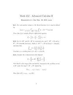


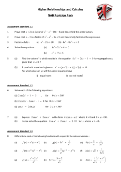

© Copyright 2026