
LogiCORE IP Asynchronous Sample Rate Converter v1.0 Product Guide
LogiCORE IP Asynchronous Sample Rate Converter v1.0 Product Guide PG039 December 18, 2012 Table of Contents SECTION I: SUMMARY IP Facts Chapter 2: Product Specification Performance. . . . . . . . . . . . . . . . . . . . . . . . . . . . . . . . . . . . . . . . . . . . . . . . . . . . . . . . . . . . . . . . . . . . . . 6 Throughput. . . . . . . . . . . . . . . . . . . . . . . . . . . . . . . . . . . . . . . . . . . . . . . . . . . . . . . . . . . . . . . . . . . . . . . 7 Resource Utilization. . . . . . . . . . . . . . . . . . . . . . . . . . . . . . . . . . . . . . . . . . . . . . . . . . . . . . . . . . . . . . . . 8 Port Descriptions . . . . . . . . . . . . . . . . . . . . . . . . . . . . . . . . . . . . . . . . . . . . . . . . . . . . . . . . . . . . . . . . . . 8 Chapter 1: Overview Feature Summary. . . . . . . . . . . . . . . . . . . . . . . . . . . . . . . . . . . . . . . . . . . . . . . . . . . . . . . . . . . . . . . . . 10 Licensing and Ordering Information . . . . . . . . . . . . . . . . . . . . . . . . . . . . . . . . . . . . . . . . . . . . . . . . . . 11 Chapter 2: Designing with the Core Functional Description. . . . . . . . . . . . . . . . . . . . . . . . . . . . . . . . . . . . . . . . . . . . . . . . . . . . . . . . . . . . . 12 Clocking. . . . . . . . . . . . . . . . . . . . . . . . . . . . . . . . . . . . . . . . . . . . . . . . . . . . . . . . . . . . . . . . . . . . . . . . . 37 Resets . . . . . . . . . . . . . . . . . . . . . . . . . . . . . . . . . . . . . . . . . . . . . . . . . . . . . . . . . . . . . . . . . . . . . . . . . . 38 System Design Considerations . . . . . . . . . . . . . . . . . . . . . . . . . . . . . . . . . . . . . . . . . . . . . . . . . . . . . . 39 SECTION II: VIVADO DESIGN SUITE Chapter 3: Customizing and Generating the Core Graphical User Interface . . . . . . . . . . . . . . . . . . . . . . . . . . . . . . . . . . . . . . . . . . . . . . . . . . . . . . . . . . . 43 Output Files . . . . . . . . . . . . . . . . . . . . . . . . . . . . . . . . . . . . . . . . . . . . . . . . . . . . . . . . . . . . . . . . . . . . . 44 Chapter 4: Constraining the Core Required Constraints . . . . . . . . . . . . . . . . . . . . . . . . . . . . . . . . . . . . . . . . . . . . . . . . . . . . . . . . . . . . . . 48 Device, Package, and Speed Grade Selections. . . . . . . . . . . . . . . . . . . . . . . . . . . . . . . . . . . . . . . . . . 48 Clock Frequencies . . . . . . . . . . . . . . . . . . . . . . . . . . . . . . . . . . . . . . . . . . . . . . . . . . . . . . . . . . . . . . . . 48 Asynchronous Sample Rate Converter v1.0 PG039 December 18, 2012 www.xilinx.com 2 SECTION III: ISE DESIGN SUITE Chapter 5: Customizing and Generating the Core Graphical User Interface . . . . . . . . . . . . . . . . . . . . . . . . . . . . . . . . . . . . . . . . . . . . . . . . . . . . . . . . . . . 51 Output Files . . . . . . . . . . . . . . . . . . . . . . . . . . . . . . . . . . . . . . . . . . . . . . . . . . . . . . . . . . . . . . . . . . . . . 52 Chapter 6: Constraining the Core Required Constraints . . . . . . . . . . . . . . . . . . . . . . . . . . . . . . . . . . . . . . . . . . . . . . . . . . . . . . . . . . . . . . 57 Device, Package, and Speed Grade Selections. . . . . . . . . . . . . . . . . . . . . . . . . . . . . . . . . . . . . . . . . . 57 Clock Frequencies . . . . . . . . . . . . . . . . . . . . . . . . . . . . . . . . . . . . . . . . . . . . . . . . . . . . . . . . . . . . . . . . 57 SECTION IV: APPENDICES Appendix A: Debugging Finding Help on Xilinx.com . . . . . . . . . . . . . . . . . . . . . . . . . . . . . . . . . . . . . . . . . . . . . . . . . . . . . . . . . 60 Debug Tools . . . . . . . . . . . . . . . . . . . . . . . . . . . . . . . . . . . . . . . . . . . . . . . . . . . . . . . . . . . . . . . . . . . . . 61 Hardware Debug . . . . . . . . . . . . . . . . . . . . . . . . . . . . . . . . . . . . . . . . . . . . . . . . . . . . . . . . . . . . . . . . . 62 Appendix B: Additional Resources Xilinx Resources . . . . . . . . . . . . . . . . . . . . . . . . . . . . . . . . . . . . . . . . . . . . . . . . . . . . . . . . . . . . . . . . . . 64 Solution Centers. . . . . . . . . . . . . . . . . . . . . . . . . . . . . . . . . . . . . . . . . . . . . . . . . . . . . . . . . . . . . . . . . . 64 References . . . . . . . . . . . . . . . . . . . . . . . . . . . . . . . . . . . . . . . . . . . . . . . . . . . . . . . . . . . . . . . . . . . . . . 64 Technical Support . . . . . . . . . . . . . . . . . . . . . . . . . . . . . . . . . . . . . . . . . . . . . . . . . . . . . . . . . . . . . . . . 65 Revision History . . . . . . . . . . . . . . . . . . . . . . . . . . . . . . . . . . . . . . . . . . . . . . . . . . . . . . . . . . . . . . . . . . 65 Notice of Disclaimer. . . . . . . . . . . . . . . . . . . . . . . . . . . . . . . . . . . . . . . . . . . . . . . . . . . . . . . . . . . . . . . 65 Asynchronous Sample Rate Converter v1.0 PG039 December 18, 2012 www.xilinx.com 3 SECTION I: SUMMARY IP Facts Overview Product Specification Designing with the Core Asynchronous Sample Rate Converter v1.0 PG039 December 18, 2012 www.xilinx.com 4 IP Facts Introduction LogiCORE IP Facts Table The LogiCORE™ IP Asynchronous Sample Rate Converter (ASRC) core converts stereo audio from one sample frequency to another. The input and output sample frequencies can be an arbitrary fraction of one another or the same frequency, but based on different clocks. The output is a band-limited version of the input resampled to match the output sample timing. Features Core Specifics Supported Device Family (1) Zynq™-7000 (2), Artix™-7, Virtex®-7, Kintex™-7 Supported User Interfaces Not Applicable Resources Provided with Core Design Files Not Provided Test Bench Not Provided Simulation Model • Typical THD+N: -130 dB (Range: -125 dB to -139 dB) Supported S/W Driver (3) • Input and output audio word width of 24 bits. • Choice of automatic ratio detection or manual ratio control. Automatic ratio detection includes rate change tracking (varispeed). Up-conversion, down-conversion, and 1:1 asynchronous conversion support Sample clock jitter rejection. Retains full performance over AES3 jitter tolerance curve [Ref 1]. • Input rates ranging from 8 kHz to 192 kHz, continuous • Output rates ranging from 8 kHz to 192 kHz, continuous • Conversion ratio ranging from 1:7.5 (down) to 8:1 (up), continuous • Low deterministic latency • Lock status outputs provided for external muting Asynchronous Sample Rate Converter v1.0 PG039 December 18, 2012 ISE: UCF Vivado: XDC Constraints File Fully asynchronous • ISE: Specify Verilog and VHDL RTL Vivado: Verilog RTL Example Design • • See Table 2-2 to Table 2-3. Verilog Behavioral N/A Tested Design Flows(4) Design Entry Simulation Synthesis ISE Design Suite v14.4 Vivado Design Suite v2012.4 Simulator tools tested. For example, Mentor Graphics ModelSim, Vivado Simulator Xilinx Synthesis Technology (XST) Vivado Synthesis Support Provided by Xilinx @ www.xilinx.com/support Notes: 1. For a complete listing of supported devices, see the release notes for this core. 2. Supported in ISE Design Suite implementations only. 3. Standalone driver details can be found in the EDK or SDK directory (<install_directory>/doc/usenglish/ xilinx_drivers.htm). Linux OS and driver support information is available from //wiki.xilinx.com . 4. For the supported versions of the tools, see the Xilinx Design Tools: Release Notes Guide. www.xilinx.com 5 Product Specification Chapter 2 Product Specification Performance Maximum Frequencies Table 2-1 lists the clock frequency performance for Virtex®-6 and Spartan®-6 FPGAs. Table 2‐1: Clock Frequency Performance Speed Grade Processing Clock Frequency (mclk) General Maximum Sample Frequency Virtex-6 all 260 MHz 192 kHz Spartan-6 -4 200 MHz 144 kHz Spartan-6 -3 175 MHz 124 kHz Spartan-6 -2 150 MHz 108 kHz FPGA Family Latency For any given conversion ratio, the latency of the design is fixed. It is determined by the phase delay of the FIR filter and fill level of the input FIFO. The FIFO level is fixed at 16, but the size of the FIR filter, and consequently its phase delay, vary in the case of down-conversion. Therefore, the formula for latency depends on whether the sample rate converted is performing up-conversion or down-conversion. The formula for determining up-conversion latency is given in Equation 2-1. The filter length is 64. Therefore, the phase delay is 32 sample periods. The latency in milliseconds depends on the input sample frequency. Latency = phase delay + FIFO delay = 32 + 16 = 48 input sample periods Equation 2‐1 The equation for down-conversion latency is given in Equation 2-2. For down-conversion, because the filter is spread across more samples, the phase delay and subsequently the latency are longer in terms of the number of input samples. Latency = phase delay + FIFO delay = (32 * fsout/fsin) + 16 Asynchronous Sample Rate Converter v1.0 PG039 December 18, 2012 www.xilinx.com Equation 2‐2 6 Chapter 2: Product Specification Latency Example 1 48 kHz: 48 kHz conversion: Latency = 32 + 16 = 48 input sample periods = 1 ms Latency Example 2 48 kHz: 96 kHz up-conversion: Latency = 32 + 16 = 48 input sample periods = 1 ms Latency Example 3 32 kHz: 48 kHz up-conversion: Latency = 32 + 16 = 48 input sample periods = 1.5 ms Latency Example 4 96 kHz: 48 kHz down-conversion: Latency = 32 • 2 + 16 = 80 input sample periods = 0.83 ms Latency Example 5 48 kHz: 44.1 kHz down-conversion: Latency = 32 • 48/44.1 + 16 = 50.83 input samples = 1.06 ms In cases of changing frequency, the latency changes smoothly as specified in Equation 2-1 and Equation 2-2. For up-conversion, changes in input sample frequency result in changes in latency, while changes in output sample frequency do not. For down-conversion, changes in input or output sample frequency result in changes in latency. Throughput The throughput of the ASRC core is determined by the input sample rate and the output sample rate. These, in turn, are limited by the processing clock frequency. See Clock Frequencies in Chapter 6 for more information. Asynchronous Sample Rate Converter v1.0 PG039 December 18, 2012 www.xilinx.com 7 Chapter 2: Product Specification Resource Utilization Resources required for the ASRC core are listed for the Virtex-6 and Spartan-6 FPGA families in Table 2-2 and for Artix-7, Kintex-7, Virtex-7, and Zynq-7000 families in Table 2-2. These values were generated using the Xilinx® CORE Generator™ tools, v14.4. They are derived from post-synthesis reports, and might change during MAP and PAR. Table 2‐2: Resource Utilization FPGA Family Registers LUTs DSP Slices RAM Blocks Virtex-6 2786 1782 12 4 Spartan-6 2688 1888 12 7 Table 2‐3: Resource Utilization Family LUTs FFs LUT‐FF pairs Slices 36k BRAMs 18k BRAMs DSP48s Artix‐7 1895 2564 2629 818 2 1 12 Kintex‐7 1871 2564 2782 890 2 1 12 Virtex‐7 1949 2564 2668 852 2 1 12 Zynq‐7000 1903 2564 2740 876 2 1 12 Port Descriptions Table 2-4 defines the ports for the ASRC core. Table 2‐4: ASRC Ports Name I/O Width mclk I 1 High frequency processing clock clkin I 1 Sample rate pulse for input samples clkout I 1 Sample rate pulse for output samples reset I 1 Asynchronous reset I 1 Manual ratio control enable. • 1 = manual mode, use manual_ratio; • 0 = use automatic ratio tracking based on the frequency of clkin and clkout I 26 Manual ratio for manual ratio mode. Fin/Fout. The format is unsigned 4.22 I 24 Input samples for stereo pair 1 channel a. Sampled at clkin. manual_ratio_en manual_ratio input_sample_1a Asynchronous Sample Rate Converter v1.0 PG039 December 18, 2012 Description www.xilinx.com 8 Chapter 2: Product Specification Table 2‐4: ASRC Ports (Cont’d) Name input_sample_1b output_sample_1a output_sample_1b fifo_level_out calc_ratio_out I/O Width I 24 Input samples for stereo pair 1 channel b. Sampled at clkin. O 24 Output samples for stereo pair 1, channel a. Valid at clkout. O 24 Output samples for stereo pair 1, channel b. Valid at clkout. O 9 Input FIFO fill level. Useful for manual ratio management. O 26 The calculated ratio Fclkout/Fclkin. The format is unsigned 4.22. O 1 Indicates that ratio tracking is in a locked state. That is, the input FIFO level is within the prescribed thresholds and stable. • 1 = locked • 0 = not locked O 1 The level of the input FIFO is beyond the safe operating range, and therefore, loss of input samples is likely. • 1 = overflow • 0 = no overflow locked fifo_overflow Asynchronous Sample Rate Converter v1.0 PG039 December 18, 2012 Description www.xilinx.com 9 Chapter 1 Overview The Asynchronous Sample Rate Converter (ASRC) core, shown in Figure 1-1, consists of two main functional units: Ratio Control and Resampler. The Ratio Control function provides ratio detection and input sample storage. The Resampler function interpolates the correct phase of the filter. Its FIR filter applies the calculated filter coefficients to the set of input samples to form an output sample. X-Ref Target - Figure 1-1 !SYNCHRONOUS 3AMPLE2ATE #ONVERTER 2ESAMPLER #OEFFICIENT -EMORY 2ATIO#ONTROL )NPUT3AMPLE #LOCK /UTPUT3AMPLE #LOCK )NPUT3AMPLES 2ATIO $ETECTION &ILTER0HASE )NTERPOLATION )NPUT 3AMPLE 3TORAGE &)2&ILTER /UTPUT 3AMPLES 8 Figure 1‐1: ASRC Top‐Level Block Diagram The Hardware Description Language (HDL) code implementing the ASRC core breaks these functions down into modules with functional boundaries. See Functional Description, page 12, for details about the functional blocks, and Modules, page 44, for descriptions of the modules and how they fit together. Feature Summary The fully asynchronous ASRC core converts stereo audio from one sample frequency to another. The input and output audio word width is 24 bits. Input and output sample frequencies can be an arbitrary fraction of one another or the same frequency, but based on different clocks. Input rates range from 8 kHz to 192 kHz, continuous. Output rates range from 8 kHz to 192 kHz, continuous. The output is a band-limited version of the input, resampled to match Asynchronous Sample Rate Converter v1.0 PG039 December 18, 2012 www.xilinx.com 10 Chapter 1: Overview the output sample timing. Conversion ratio ranges from 1:7.5 (down) to 8:1 (up), continuous. The core provides sample clock jitter rejection. It retains full performance over the AES3 jitter tolerance curve. The core uses a DSP48 slice as its main math element, and block RAM for input sample buffers and storage of the prototype filter. Licensing and Ordering Information This Xilinx LogiCORE IP module is provided at no additional cost with the Xilinx Vivado Design Suite and ISE Design Suite tools under the terms of the Xilinx End User License. Information about this and other Xilinx LogiCORE IP modules is available at the Xilinx Intellectual Property page. For information about pricing and availability of other Xilinx LogiCORE IP modules and tools, contact your local Xilinx sales representative. Asynchronous Sample Rate Converter v1.0 PG039 December 18, 2012 www.xilinx.com 11 Chapter 2 Designing with the Core This chapter includes guidelines and additional information to facilitate designing with the Asynchronous Sample Rate Converter core. Functional Description This section discusses the functional blocks found in the ASRC core, including: • Ratio Control • Input Sample Storage • Resampler Functional Block • Control Ratio Control Ratio control can be manual or automatic. In some applications, it is desirable to tweak the ratio according to an algorithm with factors other than just the audio input and output rates: for example, controlling the audio-to-video latency within a frame synchronizer. This also allows the core to be used as a fixed-rate converter. Manual Ratio Control For manual ratio control, the ratio is controlled externally and input directly into the ASRC. The values used for automatic ratio adjustment, the calculated ratio and the FIFO fill level from the input FIFO, are provided as outputs for status monitoring, and to facilitate external control. Automatic Ratio Control For automatic ratio control, a sophisticated feedback control system is used to track rate changes under varispeed conditions, yet provide stable and high-quality conversion under steady-state conditions. Automatic ratio control uses one of two algorithms depending on whether the input rate is changing. At startup, and whenever the input or output rate changes, rate-change tracking Asynchronous Sample Rate Converter v1.0 PG039 December 18, 2012 www.xilinx.com 12 Chapter 2: Designing with the Core (varispeed) mode is used to quickly adjust to the correct ratio, and to adjust the level of the input FIFO to the proper level. In this mode, the ratio correction term grows exponentially with error to quickly track large rate changes and reduce the error to low levels. See Figure 2-1. X-Ref Target - Figure 2-1 2ATIO#ORRECTION4ERM -AXIMUM4RACKABLE 3AMPLE2ATE#HANGE E NG A H G # IN TE CK A A 2 4R ,OCKED %MPTY %RROR&)&/&ILL,EVELFROM3ET0OINT Figure 2‐1: &ULL 8 Error Correction Curves Locked Mode After a small error has been achieved and the ratio is stable, an automatic switch is made to locked mode. The locked mode: • Limits the amount and rate of change of the ratio to achieve maximum audio quality. • Can track small drifts in the clock frequencies. However, if a large rate change occurs, the error term exceeds the locked range, and the mode automatically shifts to rate change tracking. When a small error is achieved and the ratio is stable, the switch to locked mode occurs again. In this manner, changes in the sample frequencies, large and small, are continuously and smoothly tracked. The input samples are buffered by the ring_buffer_gold module in the Ratio Control block. When a new output sample is required, the set of input samples required for the FIR filter convolution are sent to the resampler. Ratio Detection The Ratio Detection block is implemented in the ratio_calc and ratio_filt modules of the core. A ratio is computed by measuring the period of the input and output clock with a high-frequency clock that, in general, is not related to either the input or output clocks. This is shown in the top section of Figure 2-2. Asynchronous Sample Rate Converter v1.0 PG039 December 18, 2012 www.xilinx.com 13 Chapter 2: Designing with the Core X-Ref Target - Figure 2-2 2ATIO$ETECTION )NPUT #LOCK )NPUT0ERIOD #OUNTER $IVIDEBYN IN?COUNT #ALCULATION /UTPUT #LOCK /UTPUT0ERIOD #OUNTER $IVIDEBYN OUT?COUNT #ALCULATED2ATIO (IGH&REQ #LOCK -OVING!VERAGE &ILTER n 'AINAND"7 2EGULATION 2EGULATED 2ATIO 2EGULATION 2EFERENCE,EVEL n &)&/,EVEL 8 Figure 2‐2: Ratio Detection Block Diagram To improve the accuracy of this calculation and mitigate the effects of jitter, the input and output clocks are measured over 1024 cycles. The input period is divided by the output period to obtain a calculated ratio. To further attenuate sample clock jitter, the calculated ratio passes through a moving-average filter contained in the ratio_filt module. The moving-average filter is applied only during locked mode, when the input frequency is stable. In frequency tracking mode, the moving-average filter is bypassed. The most current calculated ratio is used for ratio regulation in this mode. To regulate the level of the input FIFO (and thus the latency), the FIFO fill level is compared with a reference level in the regulation section. The difference is used as an error signal to adjust the ratio. Because the ratio determines the position of each new output sample relative to the input samples, it effectively controls the speed at which input samples are processed. Asynchronous Sample Rate Converter v1.0 PG039 December 18, 2012 www.xilinx.com 14 Chapter 2: Designing with the Core Ratio Calculation Figure 2-3 illustrates how the input period measurement is made. The input_count block counts input clocks on each rising edge. The max_count specifies how many input clocks to count before resetting the counter. It is a parameter in the core and is nominally set to 1024. The term_cnt_in signal pulses once every max_count + 1 input clocks. This signal resets the in_period counter as well as input_count. The in_period counter counts the number of mclk cycles (mclk is the high-frequency processing clock) that occur during max_count + 1 input clocks. At every pulse of term_cnt_in, the in_period_sync register stores the latest in_period count, and the counting begins again. The in_period count resets to one so that the resulting count is the actual number of mclk cycles over the specified period, not number of cycles – 1. The in_period_sync value is shifted right by four and sent to the sample storage section as in_period_div16. X-Ref Target - Figure 2-3 IN?PERIOD?DIV CE INPUT?COUNT RST COUNT IN?PERIOD $ IN?PERIOD EN IN?PERIOD?SYNC RISINGEDGE DETECT CLK?IN COUNTSNINPUT CLOCKS MAX?COUNT 1 TERM?CNT?IN MCLK CE OUTPUT?COUNT OUT?PERIOD COUNT $ OUT?PERIOD RST RST EN OUT?PERIOD?SYNC RISINGEDGE DETECT CLK?OUT MAX?COUNT EN CALC?RATIO SHARED?DIVIDER RST COUNTSNOUTPUT CLOCKS CALC?RATIOIN?PERIOD OUT?PERIODFOUTFIN IN?PERIODCOUNTSMCLKS INNINPUTCLOCKS 2ATIO#ALCULATION CALC?RATIO 1 TERM?CNT?OUT 8 Figure 2‐3: Ratio Calculation Detailed Block Diagram The timing diagram in Figure 2-4 illustrates the operation of the ratio calculation section for the clk_in period measurement. Asynchronous Sample Rate Converter v1.0 PG039 December 18, 2012 www.xilinx.com 15 Chapter 2: Designing with the Core X-Ref Target - Figure 2-4 CLK?IN RISINGEDGEDETECT INPUT?COUNT TERM?CNT?IN IN?PERIOD IN?PERIOD?DEL COUNT COUNT COUNT 8 Figure 2‐4: Input Period Measurement Waveforms with max_count = 4 The output clock period is measured in the same fashion. The ratio is calculated based on the timing of the output clock. To obtain the calculated ratio, calc_ratio, in_period_sync is divided by out_period_sync. This is done by divide_sign_fract, a multicycle pipelined divider in the timing_control_multi_ch module. The calc_ratio signal is sent to the ratio regulation section. The calc_ratio signal allows for a range of 0 to 15 with 22 fractional bits. The calculated ratio is used internally for automatic ratio tracking, and is also output from the ASRC core to facilitate external control, if manual ratio mode is selected. Ratio Filtering for Jitter Tolerance The AES3-2003 standard [Ref 1] specifies jitter tolerance for AES receivers. This curve is shown in Figure 2-5. The AES receiver must recover the data correctly in the presence of jitter. This jitter in the timing of the audio data is propagated to the sample rate converter. Therefore, the SRC should also have jitter tolerance equivalent to that of the AES receiver. X-Ref Target - Figure 2-5 *ITTER4OLERANCE 5) *ITTER&REQUENCY(Z Figure 2‐5: - 8 Jitter Tolerance Curve In the core, the ratio is filtered for added jitter tolerance. During locked mode operation, the calculated ratio is filtered using a moving-average FIR filter to prevent short-term Asynchronous Sample Rate Converter v1.0 PG039 December 18, 2012 www.xilinx.com 16 Chapter 2: Designing with the Core variations in sampling frequency from causing harmonic distortion in the output sample stream. In other words, it attenuates the effects of input sample clock jitter. The result is no increase in distortion in the presence of jitter. Full performance is retained over the entire range of the AES3-2003 Jitter Tolerance Curve. Figure 2-6 is a block diagram of the ratio filter. It is a recursive implementation requiring only one add and one subtract. As each new data point enters, it is added into the average and the oldest data is subtracted. A shift register is used for the storage element. A 16-location shift register is implemented very efficiently in SRL elements requiring only one LUT per input data bit. The calculated ratio has 4 integer and 22 fractional bits. An additional bit of storage is used as a data valid to track data through the shift register. This bit is required for the pre-load function, which simultaneously bypasses the filter operation and pre-loads every location in the shift register with the current value of the input data. Asynchronous Sample Rate Converter v1.0 PG039 December 18, 2012 www.xilinx.com 17 Chapter 2: Designing with the Core X-Ref Target - Figure 2-6 TERM?CNT?IN TAKE?CALC?RATIO CALC?RATIO LOCKED PTR?RESET 3 2 NEW?RATIO?PENDING TAKE?NEW?RATIO PTR?RESET RESET RESET 3 DATA?EN DATA?IN MOVING?AVE? PRELOAD PRELOAD 2 DATA?IN?REG EN n SHIFT?REG MOVING?SUM AVE?OUT CALC?RATIO?FILT AVE?VALID DATA?DEL PRELOAD?OUT TK?C?RATIO?FILT 8 Figure 2‐6: Asynchronous Sample Rate Converter v1.0 PG039 December 18, 2012 Ratio Filter www.xilinx.com 18 Chapter 2: Designing with the Core When the ptr_reset input signal goes High, the preload_out flag is set High, indicating the block is in pre-load mode. The pre-load mode holds the data_in_reg, and the current data in this register is propagated directly to the moving_sum register and on to ave_out. At the same time, the shift register enable is forced active, and the shift register begins shifting in the value data_in_reg. The pre-load bit also shifts through the shift register each time in parallel with the data. When the shift register has shifted the input value through every location, the pre-load bit is at the output of the shift register in the form of preload_out. This indicates that the pre-load cycle is complete. The contents of the shift register and the output register all equal the current input value in data_in_reg. This forces a reset of the pre-load register, which returns the module to normal filtering mode. This pre-load functionality is used to bypass the moving-average filter when the ratio section is not locked (frequency tracking mode). This allows for better tracking and faster lock. When locked mode is entered, each new ratio calculated is averaged with the values pre-loaded in the shift register. The term_cnt_in input signals that a new input clock count has completed. The take_calc_ratio signal means a new output clock count has completed, as well as a divide operation to obtain calc_ratio. The combination of term_cnt_in and take_calc_ratio is used to form take_new_ratio, meaning a new data value can be taken into the moving average filter. Ratio Regulation The ratio regulation section adjusts the calculated ratio to regulate the input FIFO level (see Figure 2-7). The current fifo_level is compared with the target level, fifo_setpoint. The difference is used as an error_term that adds an offset to calc_ratio. The error term is conditioned separately for locked mode and rate change mode. Parameters in the HDL specify the gain in the error term, the error dead zone, and restrictions in the ratio slew rate, if any. These parameters establish the trade-off between tight sample rate tracking and harmonic distortion performance. The trade-off for extremely tight rate-change tracking is the presence of harmonic distortion components caused by the frequent, though minute, rate adjustments. A small dead zone in the error term (that is, an error threshold below which no adjustment is made to the ratio) makes rate adjustments happen less often. This reduces the distortion component of the rate change. However, rate-change tracking is slower and less accurate. For locked mode, the default settings in the core: • Allow a small dead zone (1/4 input-sample time). • Add no additional gain. • Allow one LSB step of rate change per output sample. The frequency-rate tracking mode has no dead zone and no additional gain. This balance: • Allows good rate-change slew. Asynchronous Sample Rate Converter v1.0 PG039 December 18, 2012 www.xilinx.com 19 Chapter 2: Designing with the Core • Allows quick, reliable recovery from loss of input. • Provides good jitter rejection. The amount and rate of the offset from the calculated ratio depends on whether or not locked mode is engaged. To enter locked mode, error_term must be less than four input samples for five consecutive term_count_out times. Unlocked mode (also called rate-change tracking mode) is entered any time the error is more than six samples. X-Ref Target - Figure 2-7 CALC?RATIO 2ATIO2EGULATION FIFO?LEVEL FIFO?SETPOINT n n ERROR?TERM ABS CLAMPSCALE OFFSET ERROR?MAG?VARI ERROR?MAG?LOCK ABS SUM?LOCK SUM?VARI n MOVE?START?PTR EN START?PTR?STEP 3 2 1 REG?RATIO 2 1 LOCKED 3 EN EN EN EN TERM?COUNT?OUT REG?RATIO 8 Figure 2‐7: Detailed Block Diagram of Ratio Regulation Section In the rate-change tracking mode, the error term is added directly to calc_ratio. It also has an exponential gain such that the correction factor is multiplied at higher error ratios. This facilitates faster locking at start-up and after frequency changes without dropping or repeating samples. In the locked mode, the error term is used to increment or decrement the ratio at a maximum rate of one LSB per output sample. The current reg_ratio is fed back and compared with the target ratio, sum_lock. If the target is different from reg_ratio, 1 is either added to or subtracted from the current ratio. The reg_ratio value is updated when the set of input samples used for the convolution changes, indicated by a pulse on move_start_ptr with a non-zero value of start_ptr_step. This limits the slew rate of the ratio to 0.24 ppm per output sample for optimal audio performance. Asynchronous Sample Rate Converter v1.0 PG039 December 18, 2012 www.xilinx.com 20 Chapter 2: Designing with the Core This mode can track slow frequency variations because calc_ratio is periodically updated, and the FIFO level is updated every output sample with subsample accuracy. This is discussed in the description of the ratio control functional block. This high degree of accuracy of fifo_level also enables the ratio detection circuit to maintain a deterministic latency when the clocks are stable. That is, for given input and output sample rates: • The latency varies by only a fraction of a sample time. • The latency for any two instances of the SRC is the same to within a fraction of a sample time. Lock Status Indicators Two top-level output signals indicate the status of the ratio control section: locked and fifo_overflow. These two signals can be used to mute the audio when: • The sample rate converter is outside its bounds of normal operation, or • The input sample rate is changing. When locked is High, the ratio control is in locked mode, with minimal FIFO level error and maximum audio quality. When locked is Low, rate-change mode is active, meaning a more aggressive rate change tracking and correspondingly lowered THD + N performance. The fifo_overflow signal indicates that the input sample FIFO has overflowed or underflowed, and therefore the output audio is corrupted. This could occur at the application or removal of the input audio stream or during extremely sharp sample rate changes. Audio quality is severely compromised when fifo_overflow is asserted. Depending on the application, rate-change tracking mode audio might or might not be acceptable. These two status bits are provided so that muting can be performed externally when instability in the sample rates could cause unacceptable distortions. Input Sample Storage The input samples are stored in a ring buffer as shown in Figure 2-8, implemented in block RAM. Two data words of 24 bits each (one for each channel of the channel pair) can be stored per memory location. The ring buffer is 48 bits wide x 512 locations deep, enough to accommodate spreading the prototype filter by a factor of 7.5 plus space to act as an input FIFO. Asynchronous Sample Rate Converter v1.0 PG039 December 18, 2012 www.xilinx.com 21 Chapter 2: Designing with the Core X-Ref Target - Figure 2-8 EN DA WRITEPTR TAT O R FILTE VEL FIFO?LE POIN MOVE TER M EN T D R PT RT STA 8 Figure 2‐8: Ring Buffer Two pointers (the write pointer and the start pointer) move through the addresses in the buffer in circular fashion. They designate the locations into which input samples are to be written, and out of which input samples are to be read for the filtering operation. Input samples are stored as they are received at the location indicated by write_ptr. The pointer is incremented each time a new sample is received. The first sample to be used in the FIR filter is indicated by start_ptr. For each output sample, a set of input samples is sent to the FIR filter, starting with the newest (at start_ptr) to the oldest (at end). The start_ptr is updated each time a new output sample is created. The locations between write_ptr and start_ptr serve as an input FIFO. The difference between the two pointers is used as the fifo_level value. This is used as a feedback mechanism for the ratio. The net effect is to change slightly the rate at which input samples are used to keep the FIFO at a predetermined level. The level is nominally 16 locations. The fifo_level value is also output from the ASRC core to facilitate external control, if manual ratio mode is selected. Input Storage Figure 2-9 is a block diagram of the input storage section. The ring buffer consists of the buffer memory (using dual-port block memory) and control logic for reading and writing. For the write port, a write-enable pulse write_en is produced on the rising edge of clkin, the input sample clock. This pulse is used to write sample data into memory and increment the address counter to the next address. Asynchronous Sample Rate Converter v1.0 PG039 December 18, 2012 www.xilinx.com 22 Chapter 2: Designing with the Core X-Ref Target - Figure 2-9 WRITE?EN WRITE?PTRADDRESS WRITEPORT EN !DDRESS #OUNTER 2ISINGEDGE DETECT CLKIN WRITE?DATA INPUT?SAMPLE "UFFER -EMORY START?PTR GO?FIR MOVE?START?PTR START?PTR?STEP 2ING"UFFER 2EAD#ONTROL READ?ADDR READPORT FETCH?SAMPLE READ?DATA DATA?VALID 8 Figure 2‐9: Input Buffer Storage Block Diagram For the read port, go_fir indicates the start of a new FIR operation to produce an output sample. This resets read_addr to the start_ptr value. The fetch_sample signal pulses once for each input sample used in the convolution. Each time it pulses, read_addr is decremented. This sends sample data to the FIR filter in the newest-to-oldest order shown in Figure 2-8. The read control also generates an integer, start_ptr. The movement of this pointer is controlled by move_start_ptr and start_ptr_step. When move_start_ptr pulses, start_ptr is increased by start_ptr_step. The outputs of this section are input samples, read_data, and a data_valid flag. Because write_ptr and start_ptr are updating at different times and possibly in different increments, the difference between them can vary widely, even if the ratio is correct and the input and output rates are perfectly stable. For example, if the ASRC core is performing a down-conversion by a factor of four, the write pointer increments four times during the time the start_ptr moves just once. For this reason, fifo_level varies by three over the period of a single output cycle. To reduce such fluctuations, fifo_level is updated only after start_ptr is updated. The fifo_level is calculated to an accuracy of 1/16th of a sample by creating sub-sample accurate write and start pointers. As shown in Figure 2-10, the fractional bits for start_ptr come from the inverse of delta_in_ctr_i. This signal indicates the position of the current output sample with respect to input samples. For this reason, it represents a fractional start position. These bits are appended to start_ptr to form start_ptr_subsamp. Asynchronous Sample Rate Converter v1.0 PG039 December 18, 2012 www.xilinx.com 23 Chapter 2: Designing with the Core X-Ref Target - Figure 2-10 RST DELTA?IN?COUNT EN WRITE?EN RST FRACT?PERIOD?COUNT WRITE?PTR EN DELTA?IN?CTR?I START?PTR n n FIFO?LEVEL FIFO?LEVEL START?PTR?SUBSAMP $IVIDE"Y MAX?COUNT IN?PERIOD?SYNC WRITE?PTR?SUBSAMP n IN?PERIOD?DIV 8 Figure 2‐10: FIFO Level Calculation with Fractional Bits The circuit in Figure 2-10 shows how the fractional bits for write_ptr are created. The in_period_sync register of the ratio calculation section contains an accurate count of the number of mclk periods in 1024 input clocks (the nominal max_count). This number is right-shifted so as to obtain the number of mclk periods in 1/16th of an input period. This number (in_period_div16) is subject to truncation errors, but it is accurate enough to use to create fractional write_ptr bits. The value in_period_div16 is used as the terminal count for the fract_period_cnt counter. The fract_period_cnt counter, then, pulses every 1/16 input sample. It is resynchronized to the updating of the write pointer by write_en, the write enable to the ring buffer. The delta_in_count counter counts each 1/16 of an input sample time. This count saturates at 15, waiting for write_en to provide a reset. For this reason, subsample bits are created for write_ptr and appended to form write_ptr_subsamp. The difference between write_ptr_subsamp and start_ptr_subsamp determines fifo_level with four fractional bits. This fifo_level changes only when start_ptr is updated and fed back to the ratio regulation section. Clock Domain Considerations The rising edge of the input and output clock must be detected in several places. Because the processing clock mclk is asynchronous to both the input and output clocks, the handling of control signals and of data crossing these clock boundaries must be done with care. First, the pulse width of the input clock and output clock must be wide enough that they are reliably sampled by mclk. Metastability can occur on occasion at clock boundaries and Asynchronous Sample Rate Converter v1.0 PG039 December 18, 2012 www.xilinx.com 24 Chapter 2: Designing with the Core should be properly handled. For example, the rising edge of the input clock is detected in the mclk clock domain. Rarely, the first register in the mclk domain experiences metastability. Except for extremely rare cases, measured in decades per event, the output of the first register settles and meets the setup requirements of the second register, so the output of the second register can be assumed to be reliable and likewise for the third register. For this reason, these can be used to detect the rising edge of the asynchronous input. Figure 2-11 shows a simple circuit that synchronizes the inputs into a new clock domain through reg_1 and reg_2, then detects the rising edge when the input to reg_3 is High, but the output is still Low. This circuit is used in the core as the interface to the input and output sample clocks. X-Ref Target - Figure 2-11 2ISING%DGE REG? REG? REG? )NPUT #LOCK 8 Figure 2‐11: Rising Edge Detect Resampler Functional Block The resampler creates a set of samples from the input samples based on the output-to-input ratio produced by the Ratio Detection section. Two major computational tasks are required to produce each output sample: • Interpolate filter coefficients for the convolution based on the prototype filter. • Perform the convolution of the interpolated coefficients with the corresponding set of input samples. Asynchronous Sample Rate Converter v1.0 PG039 December 18, 2012 www.xilinx.com 25 Chapter 2: Designing with the Core X-Ref Target - Figure 2-12 2ESAMPLER 0ROTOTYPE &ILTER #OEFFICIENT -EMORY &ILTER0OSITION2ELATIVE TO)NPUT3AMPLES &ILTER0HASE)NTERPOLATION )NPUT3AMPLES #ORRESPONDINGTO3UBFILTER &)2&ILTER /UTPUT3AMPLES 8 Figure 2‐12: Resampler Prototype Filter The prototype filter was designed using the Filter Design and Analysis tool of MATLAB®. It is a low-pass equiripple filter consisting of 64 phases of 64 taps each. This is done with a filter order of 4096 and frequency specifications of 1/64 of the desired response of each phase. The resulting coefficients are scaled by a factor of 64 to fully utilize the coefficient bit width and to maintain the signal amplitude. The prototype filter is symmetric, so only half of the coefficients are stored. Because the filter is of order 4096, there are actually 4097 coefficients. The center coefficient is stored in a 24-bit register, and the rest are stored in block RAM of size 2048 x 24. The transition band of the filter is symmetric about the Nyquist frequency: wpass = Nyquist – 9.3% wstop = Nyquist + 9.3% The resulting filter has a passband of 0.4535 times the sampling rate and a stop band of 0.5465 times the sampling rate. This yields a passband of 20 kHz for a sampling rate of 44.1 kHz, for example. The parameters used for the prototype filter in the core are shown in Table 2-1. Table 2‐1: Prototype Filter Parameters Parameter Value Response Type Low pass Design Method Equiripple Filter Order 4096 Frequency specification wpass 1/64 * 2 * 0.4535 Asynchronous Sample Rate Converter v1.0 PG039 December 18, 2012 www.xilinx.com Comment Normalized 26 Chapter 2: Designing with the Core Table 2‐1: Prototype Filter Parameters (Cont’d) Parameter Value Frequency specification wstop 1/64 * 2 * 0.5465 Magnitude specification wpass 1 Magnitude specification wstop 50000 Density Factor 16 Passband Ripple +-.016 dB Stopband Attenuation 149 dB Comment Normalized Figure 2-13 shows the frequency response of the resulting filter. X-Ref Target - Figure 2-13 -AGNITUDED" Figure 2‐13: .ORMALIZED&REQUENCYX RADSAMPLE 8 Prototype Filter Frequency Response Figure 2-14 and Figure 2-15 show calculated and measured details of the transition band, respectively, based on measurements through the sample rate converter performing a 48 kHz-to-48 kHz asynchronous conversion. X-Ref Target - Figure 2-14 -AGNITUDED" .ORMALIZED&REQUENCYXPRADSAMPLE 8 Figure 2‐14: Detail of Prototype Filter Transition Band, Calculated Asynchronous Sample Rate Converter v1.0 PG039 December 18, 2012 www.xilinx.com 27 Chapter 2: Designing with the Core X-Ref Target - Figure 2-15 D"&3 (Z Figure 2‐15: 8 Detail of Prototype Filter Transition Band, Measured Figure 2-16 and Figure 2-17 show calculated and measured details of the passband, respectively, based on measurements through the sample rate converter performing a 48 kHz-to-48 kHz asynchronous conversion. X-Ref Target - Figure 2-16 -AGNITUDED" .ORMALIZED&REQUENCYX RADSAMPLE Figure 2‐16: 8 Detail of Prototype Filter Pass Band, Calculated Asynchronous Sample Rate Converter v1.0 PG039 December 18, 2012 www.xilinx.com 28 Chapter 2: Designing with the Core X-Ref Target - Figure 2-17 D"&3 (Z Figure 2‐17: 8 Detail of Prototype Filter Pass Band, Measured Coefficient Interpolation The filter coefficients are interpolated with a third-order Lagrange interpolation according to the equation: y = – – 1 – 2 – 3 6 h0 + – 2 – 3 2 h1 + – – 1 – 3 2 h2 Equation 2‐1 + – 1 – 2 6 h3 where h0, h1, h2, and h3 are four adjacent stored coefficients. represents the difference between the location of the coefficients to be calculated (marked with an X) and h0, shown in Figure 2-18. ½ H H H &OUR3AMPLES2EQUIRED &OLLOWSA#UBIC0OLYNOMIAL 0ASSINGTHROUGH&OUR0OINTS #ONTINUOUS H 8 X-Ref Target - Figure 2-18 Figure 2‐18: Third Order Lagrange Interpolation To minimize the number of multiplications, the equation is factored to: y = – 2 * – 3 2* – – 1 *h0 3 + *h1 + * – 1 2* – – 3 *h2 + – 2 *h3 3 Equation 2‐2 The multiplications are performed using 18 x 18 multiplier blocks configured with four 18x18 multipliers in DSP48 elements. Input multiplexers and output registers for storage of intermediate results are used in conjunction with the multipliers to form multiply/adder Asynchronous Sample Rate Converter v1.0 PG039 December 18, 2012 www.xilinx.com 29 Chapter 2: Designing with the Core units. Two multiply/adder units are used in parallel for the coefficient interpolation. Each unit operates in a 16-state sequence consisting of four 4-state multiplies. Figure 2-19 is a block diagram of the coefficient interpolator. The cf_if input is the conversion factor from input samples to filter coefficients. This tells how many coefficients correspond to the distance between input samples. • For up-conversion, cf_if is 16. • For down-conversion, cf_if is 16 times the ratio of output rate to input rate. X-Ref Target - Figure 2-19 FIRST?ISAMPLE?F CURR?POSACCUM CF?IF )NTEGER0ART #OEFFICIENT!DDRESS #URRENT0OSITION IN0ROTOTYPE&ILTER &RACTIONAL0ART $ELTA 0ROTOTYPE&ILTER -EMORY 0ROTOTYPE#OEF 2EGISTERS HHHH $ELTA&ACTORS#ALCULATIONS ½ n½ n½ n½ nn½ n½ n X -ULTIPLY!DD X -ULTIPLY!DD #OEFFICIENT !CCUMULATOR COEF?ACCUM FINALADD COEF?FIR 8 Figure 2‐19: Coefficient Interpolator The input, first_sample_f, has the location of the first input sample to be used in the convolution relative to the stored filter coefficients. The curr_pos_accum register keeps track of the location of each coefficient to be accumulated relative to the stored coefficients. When a new output sample calculation is started, curr_pos_accum is initialized with first_sample_f. As a new filter coefficient is interpolated, curr_pos_accum is incremented by cf_if. This continues until the end of the stored prototype filter is reached, indicating that all the required coefficients have been interpolated and, consequently, the convolution is complete. The output of curr_pos_accum is the current position of the filter coefficient in filter space. The integer portion of this quantity is the address of the left-most stored filter coefficient to be used in the Lagrange interpolation. The fractional portion is the delta value to be used in the interpolation. The four coefficients used in the interpolation (h0, h1, h2, and h3) are retrieved serially and stored in registers during the 16-state interpolation. In the same way, several factors are calculated from the variable and stored in registers during interpolation. The related values, along with the associated stored coefficients, are sent to the two 35 x 35 multiply/add units. Asynchronous Sample Rate Converter v1.0 PG039 December 18, 2012 www.xilinx.com 30 Chapter 2: Designing with the Core The multiply/add units operate in parallel. These units multiply and sum the terms of the Lagrange interpolation. There is one final addition to produce the interpolated coefficient that is used in the FIR operation, coef_fir, as given by Figure 2-20. As each FIR coefficient is calculated, it is accumulated in the coefficient accumulator to form coef_accum, which is subsequently used to normalize the result of the convolution. • In the case of downsampling, the final coef_accum of the convolution is virtually equal to the inverse of the scaling factor required to compensate for the increased length of the convolution. • In the case of upsampling, the final coef_accum is virtually equal to 1 and serves to compensate for small amplitude distortions that might otherwise occur. FIR Filter A block diagram of the FIR Filter section is shown in Figure 2-20. X-Ref Target - Figure 2-20 SUM?SHIFT NORM?EN AUX?SEL PROD?OUT FINALOUTPUT SAMPLE REGISTERS OUTPUT?SAMP?A OUTPUT?SAMP?B OUTPUT?SAMP?C OUTPUT?SAMP?D MULT?X OSAMP?ACCUM?A OSAMP?ACCUM?B OSAMP?ACCUM?C OSAMP?ACCUM?D OUTPUTSAMPLE ACCUMULATORS AUX?B ISAMP! ISAMP" ISAMP# ISAMP$ CLAMP AUX?A INV?SUM ROUND SCALE COEF?FIR OSAMP?ACCUM?A OSAMP?ACCUM?B OSAMP?ACCUM?C OSAMP?ACCUM?D 8 Figure 2‐20: FIR Filter Block Diagram The FIR Filter section has three distinct functions: 1. Implements the resampling FIR filter for each of four channels. 2. Performs the sample normalization for each output sample, after the FIR operation is complete. 3. Serves as a general-purpose multiplier for the control section. Asynchronous Sample Rate Converter v1.0 PG039 December 18, 2012 www.xilinx.com 31 Chapter 2: Designing with the Core For FIR operation, it operates in parallel with coefficient interpolation. As each coefficient is interpolated (labeled coef_fir in the figure): 1. It is multiplied by the corresponding input sample (isamp A, B, C, or D). 2. The result is accumulated. A 35 x 35 multiplier in the FIR Filter unit performs the multiply operations. The multiplier operates on the same 16-cycle sequence as the multipliers in the coefficient interpolator. Figure 2-21 shows the sequence of operations in this multiplier. Each of the labeled cycles consists of four clocks to perform a 35 x 35 multiply. There are separate accumulators for each channel. At the end of the convolution, each accumulator holds the result of the convolution. X-Ref Target - Figure 2-21 CYCLE -ULT )SAMP! COEF )SAMP" COEF )SAMP# COEF )SAMP$ COEF 8 Figure 2‐21: Multiplier Cycles for FIR Filter For sample normalization, the accumulated sample values (osamp_accum_a, osamp_accum_b, osamp_accum_c, or osamp_accum_d) are passed back through the multiplier. They are each multiplied by the inverse of the sum of the coefficients (inv_sum). This normalizes the output samples, negating gain that might otherwise occur particularly in a downconvert situation. Because the coefficient sum can have a value from near 1 up to about 8 (in the case of down conversion by the maximum factor of 7.75), a floating-point scheme is used to preserve all significant bits through the multiply operation. The inverse sum (inv_sum) is block-normalized prior to being sent to the FIR Filter section. The sum_shift input denotes the number of non-zero integer bits and how much inv_sum was shifted to the right. Therefore, the result of the multiply must be scaled to compensate for this. Because the sum that was shifted to the right has been inverted before the multiply, the result of the multiply is also shifted to the right to compensate. This is shown in as the scale operation in Figure 2-20. A rounding operation (nearest, away from zero) to 24 bits is provided, with a corresponding enable. Because the best linearity at low amplitude is obtained with this rounding disabled, it is disabled in the core. An extra most-significant integer bit is carried through the normalization process to detect an overflow condition. If the input has high-amplitude waves with frequency components above the Nyquist rate (Fs/2), the ringing induced on the sample-rate-converted wave can cause some computed samples to exceed full-scale. In this case, the overflow is detected, and the output sample values are clamped to the maximum full scale value, either positive or negative. Asynchronous Sample Rate Converter v1.0 PG039 December 18, 2012 www.xilinx.com 32 Chapter 2: Designing with the Core This is shown as the clamp operation in Figure 2-20. Though this causes some additional distortion, it is less severe than toggling the sign bit, which would happen in the absence of clamping. Clamping, and the resulting distortion, does not come in to play in normal operation in which the input waveform frequencies are below the Nyquist rate. The final result (after scaling, rounding, and clamping) is stored in the final output sample registers. These registers are the outputs of the top-level module. Up to four audio channels (A, B, C, and D) are accommodated. More channels are accommodated by adding additional instances. The third function is a general-purpose multiplier for the control section. This function is enabled by the aux_sel input. An auxiliary set of inputs and outputs allows this unit to perform the additional, unrelated multiplications. These auxiliary multiplications are used by the control section for such functions as converting locations from input sample space to filter coefficient space. The output of the auxiliary multiplies appears on the prod_out output. Signed Fractional Divider The divide_sign_fract module is a signed 27 x 27 multicycle pipelined divider with 25 fractional output bits and a latency of 53 states. This module: • Produces the ratio and 1/ratio. • Produces the inverse of the sum of coefficients (1/ coef_accum) that is used to normalize the result of the sample accumulation. This normalization is performed in the FIR Filter section. The accuracy of these calculations directly affects the quality of the sample rate conversion. For this reason, a high degree of precision is required. Because the divide operations are done infrequently compared to other operations, the divider is optimized for minimum area, and as a result, low throughput. A round_en input to this module allows the signed fractional result be rounded to 24 bits. If enabled, the rounding function is round nearest, away from zero. In the core, this rounding is enabled. Control The high-level control is contained in the timing_control_multi_ch module. The output sample clock starts the sample calculation sequence. Each time an output sample is taken, as indicated by output_clk, a new one is calculated. While ratio detection operates more or less continuously, the resampler operates in bursts. The resampler interpolates a filter phase, performs the convolution each time an output sample is taken. It then idles until the next sample is taken and a new one can be calculated. Asynchronous Sample Rate Converter v1.0 PG039 December 18, 2012 www.xilinx.com 33 Chapter 2: Designing with the Core The idle time can be very short (for example: the output rate is very high), or the majority of the time (for example, the output rate is low, and the ratio is near 1:1) The computation starts at the rising edge of the output sample clock and terminates when the end of the prototype filter is reached. Timing Control State Machine The timing control state machine controls the creation of an output sample. Figure 2-22 is a basic diagram of the state machine. X-Ref Target - Figure 2-22 3TATUS)NPUTS #ALCULATION)NPUTS 3TATE$ELAY 2ST #OUNT 3TATE EN STATE?COUNT?TC STATE?DLY NEXT?STATE?DLY .EXT3TATE,OGIC EN NEXT?STATE CHANGE?STATE #ONTROL"IT $ECODE #ONTROL"ITS EN #ONTROL/UTPUTS #ALCULATIONS #ALCULATION/UTPUTS 8 Figure 2‐22: Timing Control The state register holds the current state. A count associated with each state determines the minimum time that each state lasts. State changes occur only when this delay is met. This is determined by the point at which the state delay count times out (indicated by state_dly_tc). The status inputs and the current state determine whether a state change occurs. The main purposes of the state machine are to: • Control access to shared multiply and divide resources Asynchronous Sample Rate Converter v1.0 PG039 December 18, 2012 www.xilinx.com 34 Chapter 2: Designing with the Core • Sequence the data • Load the results into registers at the proper time. The current state, control bits, and state counter all contribute to the control and timing of these calculations. Figure 2-23 shows the state diagram of the top-level control state machine in the timing_control_multi_ch module. 3CALE/UTPUT 3AMPLE"Y !TTENUATION&ACTOR !44%.5!4% $O.ORMALIZATION ,OAD/UTPUT 3AMPLE2EGISTERS 3CALE/UTPUT 3AMPLE"Y#OEF 3UM 3#!,% T?N $O2ATIO$IVIDE OS AM P? DO NE 0LACEHOLDER .OT5SED #URRENTLY GE #ALCULATE2ATIO 2!4)/ EW ? SA MP LE X-Ref Target - Figure 2-23 #ALC.EW 0OSITIONS !ND&ACTORS 0/3)4)/.3 )NTERPOLATE#OEFS $O&)24APS )NTERPOLATEAND!PPLY &)2 &)24AP3TATES)NCLUDE -OVING0OINTERS 8 Figure 2‐23: Top‐Level Control State Machine Timing Control State Machine States This section discusses the timing control state machine states: • RATIO State • POSITIONS State • FIR State • SCALE State • ATTENUATE State Asynchronous Sample Rate Converter v1.0 PG039 December 18, 2012 www.xilinx.com 35 Chapter 2: Designing with the Core RATIO State The initial state is RATIO. In the RATIO state, the signed fractional divider calculates the ratio from the most recent in_period_sync and out_period_sync values. The state machine remains in the RATIO state until the get_new_sample signal asserts in response to the rising edge of clkout. POSITIONS State In the POSITIONS state, a new position for the output sample relative to the input samples is calculated based on the ratio. The two sources are the regulated ratio (ratio) and the manual ratio (manual_ratio). The start position in the prototype filter is also calculated. The auxiliary functionality of the multiplier in the FIR filter section is used in some of these calculations. FIR State The bulk of the calculations happen during the FIR state. In the FIR state: • The go_fir signal pulses to indicate the start of a new FIR filter sequence. • The resampler is reset and enabled to interpolate and apply filter coefficients to the input samples. • The result is a single output sample. The state machine remains in this state until the osamp_done signal is asserted by the resampler indicating that the prototype filter has been traversed, and the FIR filter operation is completed. SCALE State The SCALE state uses divide_sign_fract to normalize the accumulated results of the FIR filter. It does so by dividing the accumulated results of the FIR by the accumulated coefficients (coef_sum). Each audio channel is normalized and clamped independently to produce the final output sample value. ATTENUATE State The optional ATTENUATE state is included as a state in which attenuation of the output can be performed for fade out or fade in, or overall magnitude control. The auxiliary multiplier functionality can be used to accomplish this. Asynchronous Sample Rate Converter v1.0 PG039 December 18, 2012 www.xilinx.com 36 Chapter 2: Designing with the Core Clocking All data processing in the Asynchronous Sample Rate Converter (ASRC) core is done in the mclk (high-speed processing clock) domain. In general, the mclk domain has no relationship to either the input or output clock. The input and output sample clocks are treated as enables that specify when input data is valid and when output data is taken. The period of the sample clocks is used to determine the conversion ratio. Timing Requirements for Input Samples Figure 2-24 shows the timing requirements for input samples. The clkin signal is resampled in the mclk domain with the circuit shown in Figure 2-11, page 25. The rising edge is used to determine when data is valid. Therefore, setup and hold times are specified in terms of output timing periods. X-Ref Target - Figure 2-24 TSU INPUT?SAMPLE CLKIN TH MCLKPERIOD INPUTDATA VALID MIN MCLKPERIOD MIN MCLKPERIOD 8 Figure 2‐24: Input Timing Relative to the rising edge of clkin, the setup requirement is zero mclk periods, and the hold requirement is five mclk periods. For accurate edge detection, the clkin signal must be High for a minimum of five mclk periods and Low for a minimum of five mclk periods. Asynchronous Sample Rate Converter v1.0 PG039 December 18, 2012 www.xilinx.com 37 Chapter 2: Designing with the Core Timing Requirements for Output Samples Figure 2-25 shows the timing characteristics for output samples. Because they are created in the mclk domain, the timing specifications are also given in terms of mclk periods. X-Ref Target - Figure 2-25 CLKOUT MIN MCLKPERIOD OUTPUT?SAMPLE OUTPUTDATAVALID TVALIDBEFORE CLKOUT MCLKPERIOD MIN MCLKPERIOD TVALIDAFTERCLKOUT MCLKPERIOD 8 Figure 2‐25: Output Timing Relative to the rising edge of clkout, output sample data is valid a minimum of three mclk periods before clkout and remains valid until the next sample is presented. The 100 mclk periods is given as a conservative minimum time that the output data is valid after the rising edge of clkout. Like clkin, clkout (an input to the ASRC) is resampled in the mclk domain to determine the output sampling rate. Because of this, clkout has a minimum High-time requirement of five mclk periods and a minimum Low time of five mclk periods Resets In general, the core does not require resets. Whenever it is not locked to the input, the core continually resets itself and tries to acquire lock. For this reason, the core resets itself and acquires lock automatically when valid input is applied. If the input audio stream is interrupted, the core resets itself and re-acquires lock when the input is restored. A reset pin is available to force a reset if needed. Asynchronous Sample Rate Converter v1.0 PG039 December 18, 2012 www.xilinx.com 38 Chapter 2: Designing with the Core System Design Considerations Audio Performance This section discusses the performance of the core in terms of: • THD+N • Maximum Conversion Ratios • Sample Frequency Ranges THD+N Typical overall THD+N performance is -133 dB. The performance varies somewhat according to the input and output sample rates and the frequency content of the signal, ranging from -125 dB to -139 dB. To illustrate the performance of the ASRC core, a 1 kHz sine tone was input into the ASRC core for two particular conversion ratios in the presence of worst-case jitter: • 48 kHz to 48 kHz • 44.1 kHz to 48 kHz A 64K point Fast Fourier Transform (FFT) was then taken of the output. Figure 2-26 shows the FFT output for the 48 kHz-to-48 kHz ratio. X-Ref Target - Figure 2-26 K(ZTOK(Z!SYNCHRONOUS D" K(Z K(Z4ONE )NJECTED#ARRIER*ITTER5) (Z 8 Figure 2‐26: FFT for 48 kHz‐to‐48 kHz Asynchronous Conversion Asynchronous Sample Rate Converter v1.0 PG039 December 18, 2012 www.xilinx.com 39 Chapter 2: Designing with the Core Figure 2-27 shows the output for the 44.1 kHz-to-48 kHz conversion. X-Ref Target - Figure 2-27 K(ZTOK(Z!SYNCHRONOUS D" K(Z K(Z4ONE )NJECTED#ARRIER*ITTER5) (Z 8 Figure 2‐27: FFT for 44.1 kHz to 48 kHz Asynchronous Conversion Table 2-2 lists performance measurements taken over several common ratios. Measurements were taken with a Prism Sound dScopeIII audio analyzer in the default THD+N measurement mode. Frequency was scanned from 20 Hz to 20 kHz. The readings hold over the jitter tolerance curve shown in Figure 2-5, page 16. These are examples of possible conversions. The ASRC core allows for virtually infinite combinations of input and output frequencies within the maximum frequency and maximum ratio constraints. Table 2‐2: THD+N Performance vs. Conversion Frequency Input Sample Frequency 32 44.1 Output Sample Frequency (kHz) 32 44.1 48 88.2 96 Min -135 -125 -125 -125 -125 Max -137 -130 -137 -133 -137 Typ -136 -127 -130 -130 -135 1 kHz -135 -128 -127 -131 -135 Min -128 -133 -125 -126 -125 Max -135 -137 -135 -137 -133 Typ -130 -136 -129 -136 -131 1 kHz -131 -135 -126 -135 -129 Asynchronous Sample Rate Converter v1.0 PG039 December 18, 2012 www.xilinx.com 40 Chapter 2: Designing with the Core Table 2‐2: THD+N Performance vs. Conversion Frequency (Cont’d) Output Sample Frequency (kHz) Input Sample Frequency 48 88.2 96 32 44.1 48 88.2 96 Min -125 -126 -135 -128 -127 Max -137 -131 -138 -132 -137 Typ -132 -128 -136 -131 -136 1 kHz -133 -127 -136 -128 -135 Min -130 -134 -129 -131 -128 Max -136 -137 -136 -137 -134 Typ -132 -136 -131 -137 -131 1 kHz -133 -136 -129 -135 -130 Min -136 -129 -136 -128 -134 Max -137 -133 -139 -134 -138 Typ -137 -131 -137 -132 -137 1 kHz -136 -130 -137 -129 -136 Maximum Conversion Ratios The maximum up-conversion ratio is 8:1. The maximum down-conversion ratio is 1:7.5. The range of the up-conversion is limited by the number of integer bits in the ratio calculation. The down-conversion ratio is limited by the amount of input sample storage memory and how much of this memory is allocated to the input FIFO. Sample Frequency Ranges The sample frequency ranges, shown in Table 2-3, are valid for a design with a 250 MHz mclk. Table 2‐3: Sample Frequency Ranges Input 8 kHz to 196 kHz Output 8 kHz to 196 kHz A slower or faster mclk reduces or increases both minimum and maximum sample frequency in approximate proportion to the change in mclk. • The upper limit is a factor of processing clock frequency. • The lower limit is a function of the width of the period counters and the processing clock frequency. Asynchronous Sample Rate Converter v1.0 PG039 December 18, 2012 www.xilinx.com 41 SECTION II: VIVADO DESIGN SUITE Customizing and Generating the Core Constraining the Core Asynchronous Sample Rate Converter v1.0 PG039 December 18, 2012 www.xilinx.com 42 Chapter 3 Customizing and Generating the Core This chapter includes information about using Xilinx tools to customize and generate the core in the Vivado™ Design Suite environment. Graphical User Interface The Asynchronous Sample Rate Converter (ASRC) core can be generated by instantiation, using the Vivado™ design tools graphical user interface (GUI). X-Ref Target - Figure 3-1 Figure 3‐1: Asynchronous Sample Rate Converter Main Screen Asynchronous Sample Rate Converter v1.0 PG039 December 18, 2012 www.xilinx.com 43 Chapter 3: Customizing and Generating the Core The screen (Figure 3-1) shows a representation of the IP symbol on the left side and the parameters on the right, which are described as follows: • Component Name: The component name is used as the base name of output files generated for the module. Names must begin with a letter and must be composed from characters: a to z, 0 to 9 and “_”. Output Files Vivado design tools generate the files necessary to build the core and places those files in the <project>/<project>.srcs/sources_1/ip/<core> directory. Modules Table 3-1 defines the modules associated with the ASRC core. Table 3‐1: ASRC Modules Module Name Description v_asrc_v1_0 This top-level wrapper instantiates and connects the lower-level modules and provides the I/O interface. v_asrc_v1_0_timing_control_multi_ch Contains the master state machine that controls the creation of each output sample. Instantiates the divider that is used for ratio calculation and normalizing the output samples. v_asrc_v1_0_divide_sign_fract 27 x 27 bit signed serial divider. The quotient has 27 integer and 26 fractional bits. This divider is used to: • calculate the ratio of output sample rate to input sample rate, and • normalize output samples based on the sum of input coefficients. v_asrc_v1_0_ring_buffer_gold Pointers and control for the ring buffer memory. The ring buffer stores incoming samples and provides the sample stream to fir_gold. One instance is required for each pair of channels. v_asrc_v1_0_buffer_mem_gold 48 x 512 dual-port RAM for the ring buffer. v_asrc_v1_0_ratio_calc This module contains the counters for determining input and output sample rates. These rates are sent to the shared divider and the calculated ratio is returned. It also determines the feedback error term based on FIFO level and regulates the ratio accordingly. v_asrc_v1_0_ratio_filt Instantiates moving_ave_26 and determines when a new ratio has been calculated, and when the filter should be bypassed. Asynchronous Sample Rate Converter v1.0 PG039 December 18, 2012 www.xilinx.com 44 Chapter 3: Customizing and Generating the Core Table 3‐1: ASRC Modules (Cont’d) Module Name Description v_asrc_v1_0_moving_ave_26 Performs a 16-tap moving average filter on the calculated ratio. v_asrc_v1_0_filt_interp_gold Performs the Lagrange interpolation on the prototype filter. Interpolates a filter coefficient for every input sample in the FIR filter operation. v_asrc_v1_0_filt_mem_gold 24 x 2048 single port ROM containing the prototype filter. The prototype filter is 4097 coefficients and symmetrical. The middle coefficient is stored separately. v_asrc_v1_0_mult35x35_hdl 35 x 35 multiplier using four DSP slices. The multipliers are inferred from HDL code. v_asrc_v1_0_mult_one_third_dual Constant coefficient multiplier implements a divide by 3 on a 24-bit number. Performs two multiplies in a time-slice fashion. v_asrc_v1_0_fir_gold_4ch Performs a 64-tap FIR filter for each output sample for up to four channels. One instance is required for each set of four channels. Data comes from filt_interp_gold. Coefficients come from filt_interp_gold. Asynchronous Sample Rate Converter v1.0 PG039 December 18, 2012 www.xilinx.com 45 Chapter 3: Customizing and Generating the Core Module Hierarchy Figure 3-2 shows the hierarchy of the modules and their relation to the functional blocks. X-Ref Target - Figure 3-2 TIMING?CONTROL SHARED?DIVIDER?V? )NPUT3AMPLE3TORAGE RING?BUFFER?GOLD BUFFER?MEM?GOLD 2ATIO$ETECTION RATIO?CALC RATIO?FILT MOVING?AVE? #OEFFICIENT-EMORY FILT?MEM?GOLD ASRC?GOLD &ILTER0HASE)NTERPOLATION -5,48?3%15%.4)!,?0)0% FILT?INTERP?GOLD -5,48?3%15%.4)!,?0)0% MULT?ONE?THIRD MULT?ONE?THIRD &)2&ILTER FIR?GOLD -5,48?3%15%.4)!,?0)0% 8 Figure 3‐2: Module Hierarchy and Relation to Functional Blocks X-Ref Target - Figure 3-3 Verilog Output Files Table 3-2 lists the Verilog output files generated by Vivado design tools. Asynchronous Sample Rate Converter v1.0 PG039 December 18, 2012 www.xilinx.com 46 Chapter 3: Customizing and Generating the Core Table 3‐2: Verilog Output Files Name Description <component_name>.veo The HDL template for instantiating the core <component_name>.xci IP-XACT file describing which options were used to generate the core. An XCI file can also be used as a source file for Vivado. <component_name>.xml IP-XACT XML file describing how the core is constructed so Vivado can properly build the core. <component name>/hdl/verilog/ v_asrc_v1_0_buffer_mem_gold.v <component name>/hdl/verilog/ v_asrc_v1_0_divide_sign_fract.v <component name>/hdl/verilog/ v_asrc_v1_0_filt_interp_gold.v <component name>/hdl/verilog/ v_asrc_v1_0_filter_mem_gold.v <component name>/hdl/verilog/v_asrc_v1_0_fir_gold_4ch.v <component name>/hdl/verilog/ v_asrc_v1_0_moving_ave_26.v <component name>/hdl/verilog/ v_asrc_v1_0_mult35x35_hdl.v Verilog source output files. <component name>/hdl/verilog/ v_asrc_v1_0_mult_one_third_dual.v <component name>/hdl/verilog/v_asrc_v1_0_ratio_calc.v <component name>/hdl/verilog/v_asrc_v1_0_ratio_filt.v <component name>/hdl/verilog/ v_asrc_v1_0_ring_buffer_gold.v <component name>/hdl/verilog/ v_asrc_v1_0_shift_reg_27x16.v <component name>/hdl/verilog/ v_asrc_v1_0_timing_control_multi_ch.v <component name>/hdl/verilog/v_asrc_v1_0.v /hdl/<component name>.xdc Asynchronous Sample Rate Converter v1.0 PG039 December 18, 2012 Constraints File (XDC) www.xilinx.com 47 Chapter 4 Constraining the Core This chapter contains information about constraining the core in the Vivado™ Design Suite environment. Required Constraints The delivered Constraint File (XDC) provides constraints, specifically multicycle path constraints. These constraints ease timing on certain paths to make higher mclk performance possible. The mclk is the only signal that is used as a clock. A sample of this constraint is included below. It should be modified according to the conversion ratios desired and the target device. create_clock -name mclk -period 6.666 [get_ports mclk] Device, Package, and Speed Grade Selections The frequency of the processing clock (mclk) determines which range of audio frequencies can be converted. The device and speed grade selection should be made with the target mclk frequency in mind. Clock Frequencies The minimum required processing clock frequencies for up-conversion is shown in Equation 4-1. Fmclk = Fsout * 1350 Equation 4‐1 The minimum required frequency for down-conversion is shown in Equation 4-2. Fmclk = Fsin * 1030 + Fsout * 295 Asynchronous Sample Rate Converter v1.0 PG039 December 18, 2012 www.xilinx.com Equation 4‐2 48 Chapter 4: Constraining the Core For example, a down-conversion from 192 kHz to 48 kHz requires a clock frequency of 192 kHz x 1030 + 48 kHz x 295 = 221.72. See Performance in Chapter 2 for the clock frequency performance of the FPGA families. Table 4-1 shows approximate clock frequencies required for some common conversions. These values reflect the formulas for up-conversion and down-conversion. Table 4‐1: Approximate Processing Clock Frequencies (MHz) Required for Various Conversions Output Sample Frequency (kHz) Input Sample Frequency (kHz) 32 44.1 48 88.2 96 144 192 32 45 60 65 120 130 195 260 44.1 55 60 65 120 130 195 260 48 60 65 65 120 130 195 260 88.2 105 105 110 120 130 195 260 96 110 115 115 125 130 195 260 144 160 165 165 175 180 195 260 192 210 215 215 225 230 245 260 Asynchronous Sample Rate Converter v1.0 PG039 December 18, 2012 www.xilinx.com 49 SECTION III: ISE DESIGN SUITE Customizing and Generating the Core Constraining the Core Asynchronous Sample Rate Converter v1.0 PG039 December 18, 2012 www.xilinx.com 50 Chapter 5 Customizing and Generating the Core This chapter includes information about using Xilinx tools to customize and generate the core in the ISE® Design Suite environment. Graphical User Interface The Asynchronous Sample Rate Converter (ASRC) core can be generated by instantiation, using the CORE Generator™ tool graphical user interface (GUI). X-Ref Target - Figure 5-1 Figure 5‐1: Asynchronous Sample Rate Converter Main Screen The only input required in the GUI is the Component Name. The Component Name is used as the base name of output files generated for the module. The Component Name, shown in Figure 5-1, is v_asrc. Asynchronous Sample Rate Converter v1.0 PG039 December 18, 2012 www.xilinx.com 51 Chapter 5: Customizing and Generating the Core Output Files This section lists the modules associated with the ASRC core as well as the output files that are created when the core is generated. The output files depend upon whether the design entry is VHDL or Verilog. Modules Table 5-1 defines the modules associated with the ASRC (VHDL) core. Table 5‐1: ASRC Modules Module Name Description v_asrc_v1_0 This top-level wrapper instantiates and connects the lower-level modules and provides the I/O interface. timing_control_multi_ch Contains the master state machine that controls the creation of each output sample. Instantiates the divider that is used for ratio calculation and normalizing the output samples. divide_sign_fract 27 x 27 bit signed serial divider. The quotient has 27 integer and 26 fractional bits. This divider is used to: • calculate the ratio of output sample rate to input sample rate, and • normalize output samples based on the sum of input coefficients. ring_buffer_gold Pointers and control for the ring buffer memory. The ring buffer stores incoming samples and provides the sample stream to fir_gold. One instance is required for each pair of channels. buffer_mem_gold 48 x 512 dual-port RAM for the ring buffer. ratio_calc This module contains the counters for determining input and output sample rates. These rates are sent to the shared divider and the calculated ratio is returned. It also determines the feedback error term based on FIFO level and regulates the ratio accordingly. ratio_filt Instantiates moving_ave_26 and determines when a new ratio has been calculated, and when the filter should be bypassed. moving_ave_26 Performs a 16-tap moving average filter on the calculated ratio. filt_interp_gold Performs the Lagrange interpolation on the prototype filter. Interpolates a filter coefficient for every input sample in the FIR filter operation. filt_mem_gold 24 x 2048 single port ROM containing the prototype filter. The prototype filter is 4097 coefficients and symmetrical. The middle coefficient is stored separately. mult35x35_hdl 35 x 35 multiplier using four DSP slices. The multipliers are inferred from HDL code. Asynchronous Sample Rate Converter v1.0 PG039 December 18, 2012 www.xilinx.com 52 Chapter 5: Customizing and Generating the Core Table 5‐1: ASRC Modules (Cont’d) Module Name Description mult_one_third_dual Constant coefficient multiplier implements a divide by 3 on a 24-bit number. Performs two multiplies in a time-slice fashion. fir_gold_4ch Performs a 64-tap FIR filter for each output sample for up to four channels. One instance is required for each set of four channels. Data comes from filt_interp_gold. Coefficients come from filt_interp_gold. Module Hierarchy Figure 5-2 shows the hierarchy of the modules and their relation to the functional blocks. X-Ref Target - Figure 5-2 TIMING?CONTROL SHARED?DIVIDER?V? )NPUT3AMPLE3TORAGE RING?BUFFER?GOLD BUFFER?MEM?GOLD 2ATIO$ETECTION RATIO?CALC RATIO?FILT MOVING?AVE? #OEFFICIENT-EMORY FILT?MEM?GOLD ASRC?GOLD &ILTER0HASE)NTERPOLATION -5,48?3%15%.4)!,?0)0% FILT?INTERP?GOLD -5,48?3%15%.4)!,?0)0% MULT?ONE?THIRD MULT?ONE?THIRD &)2&ILTER FIR?GOLD -5,48?3%15%.4)!,?0)0% 8 Figure 5‐2: Module Hierarchy and Relation to Functional Blocks X-Ref Target - Figure 5-3 Asynchronous Sample Rate Converter v1.0 PG039 December 18, 2012 www.xilinx.com 53 Chapter 5: Customizing and Generating the Core VHDL Design Entry Files Table 5-2 lists the VHDL output files in the CORE Generator tool. Table 5‐2: VHDL Output Files Name Description <component_name>_readme.txt Readme file for the core. <component_name>.vho <component_name>_synth.vhd Template files containing code that can be used as a model for instantiating a CORE Generator tool module in an HDL design. <component_name>.xco Log file from the CORE Generator tool describing which options were used to generate the core. An XCO file can also be used as an input to the CORE Generator tool. <component_name>_flist.txt A text file listing all of the output files produced when the customized core was generated in the CORE Generator tool. <component_name>.asy Graphical symbol information file. Used by the ISE® tools and some third-party tools to create a symbol representing the core. <component_name>.gise <component_name>.xise ISE tool subproject files for use when including the core in ISE tool designs. <component name>/hdl/vhdl/buffer_mem_gold.vhd <component name>/hdl/vhdl/divide_sign_fract.vhd <component name>/hdl/vhdl/filt_interp_gold.vhd <component name>/hdl/vhdl/filter_mem_gold.vhd <component name>/hdl/vhdl/fir_gold_4ch.vhd <component name>/hdl/vhdl/moving_ave_26.vhd <component name>/hdl/vhdl/mult35x35_hdl.vhd <component name>/hdl/vhdl/mult_one_third_dual.vhd VHDL Source output files <component name>/hdl/vhdl/ratio_calc.vhd <component name>/hdl/vhdl/ratio_filt.vhd <component name>/hdl/vhdl/ring_buffer_gold.vhd <component name>/hdl/vhdl/shift_reg_27x16.vhd <component name>/hdl/vhdl/timing_control_multi_ch.vhd <component name>/hdl/vhdl/v_asrc_v1_0.vhd <component name>/hdl/v_asrc_v1_0.ucf Asynchronous Sample Rate Converter v1.0 PG039 December 18, 2012 User Constraints File (UCF) www.xilinx.com 54 Chapter 5: Customizing and Generating the Core Verilog Design Entry Files Table 5-3 lists the Verilog output files in the CORE Generator tool. Table 5‐3: Verilog Output Files Name Description <component_name>_readme.txt Readme file for the core. Template files containing code that can be used as a model for instantiating a CORE Generator tool module in an HDL design. <component_name>.veo <component_name>_synth.v <component_name>.xco Log file from the CORE Generator tool describing which options were used to generate the core. An XCO file can also be used as an input to the CORE Generator tool. <component_name>_flist.txt A text file listing all of the output files produced when the customized core was generated in the CORE Generator tool. <component_name>.asy Graphical symbol information file. Used by the ISE tools and some third-party tools to create a symbol representing the core. <component_name>.gise ISE tool subproject files for use when including the core in ISE tool designs. <component_name>.xise Asynchronous Sample Rate Converter v1.0 PG039 December 18, 2012 www.xilinx.com 55 Chapter 5: Customizing and Generating the Core Table 5‐3: Verilog Output Files (Cont’d) Name Description <component name>/hdl/verilog/v_asrc_v1_0_buffer_mem_gold.v <component name>/hdl/verilog/v_asrc_v1_0_divide_sign_fract.v <component name>/hdl/verilog/v_asrc_v1_0_filt_interp_gold.v <component name>/hdl/verilog/v_asrc_v1_0_filter_mem_gold.v <component name>/hdl/verilog/v_asrc_v1_0_fir_gold_4ch.v <component name>/hdl/verilog/v_asrc_v1_0_moving_ave_26.v <component name>/hdl/verilog/v_asrc_v1_0_mult35x35_hdl.v <component name>/hdl/verilog/v_asrc_v1_0_mult_one_third_dual.v Verilog source output files. <component name>/hdl/verilog/v_asrc_v1_0_ratio_calc.v <component name>/hdl/verilog/v_asrc_v1_0_ratio_filt.v <component name>/hdl/verilog/v_asrc_v1_0_ring_buffer_gold.v <component name>/hdl/verilog/v_asrc_v1_0_shift_reg_27x16.v <component name>/hdl/verilog/v_asrc_v1_0_timing_control_multi_ch.v <component name>/hdl/verilog/v_asrc_v1_0.v <component name>/hdl/v_asrc_v1_0.ucf Asynchronous Sample Rate Converter v1.0 PG039 December 18, 2012 www.xilinx.com User Constraints File (UCF) 56 Chapter 6 Constraining the Core This chapter contains information about constraining the core in the ISE® Design Suite environment. Required Constraints The delivered User Constraint File (UCF) provides constraints, specifically multicycle path constraints. These constraints ease timing on certain paths to make higher mclk performance possible. The mclk is the only signal that is used as a clock. A constraint for this clock is included in the UCF. It should be modified according to the conversion ratios desired and the target device. Device, Package, and Speed Grade Selections The frequency of the processing clock (mclk) determines which range of audio frequencies can be converted. The device and speed grade selection should be made with the target mclk frequency in mind. Clock Frequencies The minimum required processing clock frequencies for up-conversion is shown in Equation 6-1. Fmclk = Fsout * 1350 Equation 6‐1 The minimum required frequency for down-conversion is shown in Equation 6-2. Fmclk = Fsin * 1030 + Fsout * 295 Asynchronous Sample Rate Converter v1.0 PG039 December 18, 2012 www.xilinx.com Equation 6‐2 57 Chapter 6: Constraining the Core For example, a down-conversion from 192 kHz to 48 kHz requires a clock frequency of 192 kHz x 1030 + 48 kHz x 295 = 221.72. See Performance in Chapter 2 for the clock frequency performance of the FPGA families. Table 6-1 shows approximate clock frequencies required for some common conversions. These values reflect the formulas for up-conversion and down-conversion. Table 6‐1: Approximate Processing Clock Frequencies (MHz) Required for Various Conversions Output Sample Frequency (kHz) Input Sample Frequency (kHz) 32 44.1 48 88.2 96 144 192 32 45 60 65 120 130 195 260 44.1 55 60 65 120 130 195 260 48 60 65 65 120 130 195 260 88.2 105 105 110 120 130 195 260 96 110 115 115 125 130 195 260 144 160 165 165 175 180 195 260 192 210 215 215 225 230 245 260 Asynchronous Sample Rate Converter v1.0 PG039 December 18, 2012 www.xilinx.com 58 SECTION IV: APPENDICES Debugging Additional Resources Asynchronous Sample Rate Converter v1.0 PG039 December 18, 2012 www.xilinx.com 59 Appendix A Debugging This appendix includes details about resources available on the Xilinx Support website and debugging tools. In addition, this appendix provides suggestions for debugging the Asynchronous Sample Rate Converter core. The following topics are included in this appendix: • Finding Help on Xilinx.com • Debug Tools • Hardware Debug Finding Help on Xilinx.com To help in the design and debug process when using the Asynchronous Sample Rate Converter, the Xilinx Support web page (www.xilinx.com/support) contains key resources such as product documentation, release notes, answer records, information about known issues, and links for opening a Technical Support WebCase. Documentation This product guide is the main document associated with the Asynchronous Sample Rate Converter. This guide, along with documentation related to all products that aid in the design process, can be found on the Xilinx Support web page (www.xilinx.com/support) or by using the Xilinx Documentation Navigator. Download the Xilinx Documentation Navigator from the Design Tools tab on the Downloads page (www.xilinx.com/download). For more information about this tool and the features available, open the online help after installation. Release Notes Known issues for all cores, including the Asynchronous Sample Rate Converter are described in the IP Release Notes Guide (XTP025). Asynchronous Sample Rate Converter v1.0 PG039 December 18, 2012 www.xilinx.com 60 Appendix A: Debugging Known Issues Answer Records include information about commonly encountered problems, helpful information on how to resolve these problems, and any known issues with a Xilinx product. Answer Records are created and maintained daily ensuring that users have access to the most accurate information available. Answer Records for this core are listed below, and can also be located by using the Search Support box on the main Xilinx support web page. To maximize your search results, use proper keywords such as • Product name • Tool message(s) • Summary of the issue encountered A filter search is available after results are returned to further target the results. Contacting Technical Support Xilinx provides premier technical support for customers encountering issues that require additional assistance. To contact Xilinx Technical Support: 1. Navigate to www.xilinx.com/support. 2. Open a WebCase by selecting the WebCase link located under Support Quick Links. When opening a WebCase, include: • Target FPGA including package and speed grade. • All applicable Xilinx Design Tools and simulator software versions. • Additional files based on the specific issue might also be required. See the relevant sections in this debug guide for guidelines about which file(s) to include with the WebCase. Debug Tools There are many tools available to address Asynchronous Sample Rate Converter design issues. It is important to know which tools are useful for debugging various situations. Asynchronous Sample Rate Converter v1.0 PG039 December 18, 2012 www.xilinx.com 61 Appendix A: Debugging ChipScope Pro Tool The ChipScope™ Pro debugging tool inserts logic analyzer, bus analyzer, and virtual I/O cores directly into your design. The ChipScope Pro debugging tool allows you to set trigger conditions to capture application and integrated block port signals in hardware. Captured signals can then be analyzed through the ChipScope Pro logic analyzer tool. For detailed information for using the ChipScope Pro debugging tool, see www.xilinx.com/tools/ cspro.htm. Vivado Lab Tools Vivado Lab Tools inserts logic analyzer, bus analyzer, and virtual I/O cores directly into your design. Vivado Lab Tools allows you to set trigger conditions to capture application and integrated block port signals in hardware. Captured signals can then be analyzed. Hardware Debug This section provides debug steps for common issues. The ChipScope debugging tool is a valuable resource to use in hardware debug. The signal names mentioned in the following individual sections can be probed using the ChipScope debugging tool for debugging the specific problems. Details are provided on: • General Checks • ASRC specific debug tips. General Checks Ensure that all the timing constraints for the core were properly incorporated and that all constraints were met during implementation. • Does it work in post-place and route timing simulation? If problems are seen in hardware but not in timing simulation, this could indicate a PCB issue. Ensure that all clock sources are active and clean. • If using MMCMs in the design, ensure that all MMCMs have obtained lock by monitoring the LOCKED port. It is important to understand that mclk is the only signal that is used as a clock in the ASRC. The clkin and clkout audio rate pulses are sampled on mclk and used to determine when new data is present on the input, and when data has been taken on the output. These pulses are also used to determine the ratio of output sample rate to input sample rate which regulates the filtering operations. Since clkin and clkout are sampled asynchronously, it Asynchronous Sample Rate Converter v1.0 PG039 December 18, 2012 www.xilinx.com 62 Appendix A: Debugging is important that they be wide enough, and that the data meets the timing requirements described in the Clocking in Chapter 2. The main signals useful for debug are “locked” and “overflow”. In automatic ratio mode, the locked bit will go high, and the overflow bit will go low within about 2s of when clkin and clkout are applied and stable. Both of these signals are derived by looking at the level of the input FIFO. The automatic ratio mode seeks to keep the input FIFO level in a very narrow range near 16, meaning that the FIFO is not filling or emptying, but rather, maintaining a constant level. When this target level is maintained for several thousand sample times, the locked bit is asserted. The overflow bit indicates that the FIFO level differs from the target level by a 16 or more, such that input samples may be lost from the FIFO causing severe degradation in audio quality. If the ratio of the input to output clocks is known to a high degree of accuracy, manual ratio mode can be used for diagnostic purposes. The ratio can be applied in manual mode to test the quality of the ASRC filtering. Note in manual mode, “locked” and “overflow” are still operational, although it is not essential that “locked” be asserted to get maximum audio quality. If the manual ratio matches, or tracks the actual ratio of the clocks, then the FIFO level should be stable, as indicated by fifo_level_out. If this is the case, the output audio quality will be good, even though the FIFO level is not precisely at the target. On the other hand, if overflow is asserted, it means there is a danger of the samples being dropped from the FIFO, affecting output audio quality. Therefore it is important, even in manual mode, that the FIFO level (fifo_level_out) be maintained within the limits 0-32. In manual mode, a close approximation of the ratio is calculated and output on the calc_ratio_out. It is useful to examine this calculated ratio to know the approximate ratio that is used in the automatic ratio mode, however this calculated ratio is only accurate to approximately .2%, and is thus not stable enough to use directly as the manual_ratio input. The manual_ratio must be much more accurate to operate for a sustained period of time without overflow/underflow. Asynchronous Sample Rate Converter v1.0 PG039 December 18, 2012 www.xilinx.com 63 Appendix B Additional Resources Xilinx Resources For support resources such as Answers, Documentation, Downloads, and Forums, see the Xilinx Support website at: www.xilinx.com/support. For a glossary of technical terms used in Xilinx documentation, see: www.xilinx.com/company/terms.htm. Solution Centers See the Xilinx Solution Centers for support on devices, software tools, and intellectual property at all stages of the design cycle. Topics include design assistance, advisories, and troubleshooting tips. References These documents provide supplemental material useful with this product guide: 1. Audio Engineering Society, Inc. (www.aes.org) ° AES5-2003, AES Recommended Practice for Professional Digital Audio-Preferred sampling frequencies for applications employing pulse-code modulation ° AES3-2003, AES Recommended Practice for Digital Audio Engineering-Serial transmission format for two-channel linearly represented digital audio data 2. Vivado™ Design Suite user documentation (www.xilinx.com/cgi-bin/docs/ rdoc?v=2012.3;t=vivado+docs) Asynchronous Sample Rate Converter v1.0 PG039 December 18, 2012 www.xilinx.com 64 Appendix B: Additional Resources Technical Support Xilinx provides technical support at www.xilinx.com/support for this LogiCORE™ IP product when used as described in the product documentation. Xilinx cannot guarantee timing, functionality, or support of product if implemented in devices that are not defined in the documentation, if customized beyond that allowed in the product documentation, or if changes are made to any section of the design labeled DO NOT MODIFY. See the IP Release Notes Guide (XTP025) for more information on this core. For each core, there is a master Answer Record that contains the Release Notes and Known Issues list for the core being used. The following information is listed for each version of the core: • New Features • Resolved Issues • Known Issues Revision History The following table shows the revision history for this document. Date Version Revision 04/24/12 1.0 Initial Xilinx release. 12/18/12 1.1 Updated for tools versions, added Vivado section, and updated the Debugging appendix. Notice of Disclaimer The information disclosed to you hereunder (the “Materials”) is provided solely for the selection and use of Xilinx products. To the maximum extent permitted by applicable law: (1) Materials are made available “AS IS” and with all faults, Xilinx hereby DISCLAIMS ALL WARRANTIES AND CONDITIONS, EXPRESS, IMPLIED, OR STATUTORY, INCLUDING BUT NOT LIMITED TO WARRANTIES OF MERCHANTABILITY, NON-INFRINGEMENT, OR FITNESS FOR ANY PARTICULAR PURPOSE; and (2) Xilinx shall not be liable (whether in contract or tort, including negligence, or under any other theory of liability) for any loss or damage of any kind or nature related to, arising under, or in connection with, the Materials (including your use of the Materials), including for any direct, indirect, special, incidental, or consequential loss or damage (including loss of data, profits, goodwill, or any type of loss or damage suffered as a result of any action brought by a third party) even if such damage or loss was reasonably foreseeable or Xilinx had been advised of the possibility of the same. Xilinx assumes no obligation to correct any errors contained in the Materials or to notify you of updates to the Materials or to product specifications. You may not reproduce, modify, distribute, or publicly display the Materials without prior written consent. Certain products are subject to the terms and conditions of the Limited Warranties which can be viewed at http://www.xilinx.com/warranty.htm; IP cores may be subject to warranty and support terms contained in a license issued to you by Xilinx. Xilinx products are not designed or intended to be fail-safe or for use in any application requiring fail-safe performance; you assume sole risk and liability for use of Xilinx products in Critical Applications: http://www.xilinx.com/ warranty.htm#critapps. Asynchronous Sample Rate Converter v1.0 PG039 December 18, 2012 www.xilinx.com 65 Appendix B: Additional Resources © Copyright 2012 Xilinx, Inc. Xilinx, the Xilinx logo, Artix, ISE, Kintex, Spartan, Virtex, Vivado, Zynq, and other designated brands included herein are trademarks of Xilinx in the United States and other countries. All other trademarks are the property of their respective owners. Asynchronous Sample Rate Converter v1.0 PG039 December 18, 2012 www.xilinx.com 66


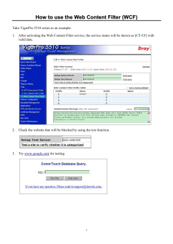


© Copyright 2026