
NCP349GEVB NCP349 Evaluation Board User's Manual
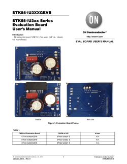
NCP349GEVB
NCP349 Evaluation Board
User's Manual
Description
The NCP349 is able to disconnect the systems from its output pin
when wrong input operating conditions are detected. The system is
positive overvoltage protected up to +28 V.
This device uses an internal NMOS and therefore, no external
device is necessary, reducing the system cost and the PCB area of the
application board. The NCP349 is able to instantaneously disconnect
the output from the input, due to integrated Low RON Power NMOS
(65 mW), if the input voltage exceeds the overvoltage threshold
(OVLO) or falls below the undervoltage threshold (UVLO).
The NCP349 provides a negative going flag (FLAG) output, which
alerts the system that a fault has occurred. In addition, the device has
ESD-protected input (15 kV Air) when bypassed with a 1.0 mF or
larger capacitor.
http://onsemi.com
EVAL BOARD USER’S MANUAL
Figure 1. NCP349GEVB Board Picture
© Semiconductor Components Industries, LLC, 2011
August, 2011 − Rev. 2
1
Publication Order Number:
EVBUM2014/D
NCP349GEVB
Figure 2. NCP349GEVB Board Schematic
http://onsemi.com
2
NCP349GEVB
PCB
Figure 3. NCP349GEVB Board Layout (Top View)
Figure 4. NCP349GEVB Board Layout (Bottom View)
http://onsemi.com
3
NCP349GEVB
Table 1. BILL OF MATERIALS
Quantity
Designation
Manufacturer
1
NCP349 LLGA3x3
ON Semiconductor
Digi key
Specifications
1
C1 (Cin)
Murata −
GRM188R61E105KA12D
490−3897−1−ND
2
INPUT and OUTPUT
connectors
Kontec Comatel
5001K−ND
1 pin. 2.54 PCB Single ligne
3
Test points: FLAG, EN,
VCC
Kontec Comatel
5001K−ND
1 pin. 2.54 PCB Single ligne
1
EN_state. EN connection
to GND pull down or to
+5 V pull up
Kontec Comatel
5001K−ND
3 pins. 2.54 PCB Single ligne
2
R1, R2
susumu
Rr08p(value)dct−nd
2
GND jumper
Over voltage protection
WM8083−ND
1 mF 25V X5R CMS0805
100 kW . CMS0603 0.5%
Jumper Ground 1 mm pitch 10.16 mm
CONNECTING PROCESS
Turn On.
1. Connect a supply (5 V typical, Maximum rating, 7 V) on Vcc test point.
2. Let EN_STATE strap on right side if you want to Enable the device. (Pull down to GND).
3. Connect Vin on INPUT test point. Typical UVLO current consumption is 70 mA. Typical current consumption
UVLO < Vin < OVLO without load is 170 mA.
4. Connect the system on OUTPUT test point.
5. Increase Vin level above UVLO to see Vin on Vout pin.
6. Connect strap on left side to disable the part (disconnect Vout from Vin)
Turn Off.
1. Disconnect system connected on Vout connector.
2. Disconnect Vin or adapter connected on Vin connector.
3. Disconnect Vcc supply.
ON Semiconductor and
are registered trademarks of Semiconductor Components Industries, LLC (SCILLC). SCILLC reserves the right to make changes without further notice
to any products herein. SCILLC makes no warranty, representation or guarantee regarding the suitability of its products for any particular purpose, nor does SCILLC assume any liability
arising out of the application or use of any product or circuit, and specifically disclaims any and all liability, including without limitation special, consequential or incidental damages.
“Typical” parameters which may be provided in SCILLC data sheets and/or specifications can and do vary in different applications and actual performance may vary over time. All
operating parameters, including “Typicals” must be validated for each customer application by customer’s technical experts. SCILLC does not convey any license under its patent rights
nor the rights of others. SCILLC products are not designed, intended, or authorized for use as components in systems intended for surgical implant into the body, or other applications
intended to support or sustain life, or for any other application in which the failure of the SCILLC product could create a situation where personal injury or death may occur. Should
Buyer purchase or use SCILLC products for any such unintended or unauthorized application, Buyer shall indemnify and hold SCILLC and its officers, employees, subsidiaries, affiliates,
and distributors harmless against all claims, costs, damages, and expenses, and reasonable attorney fees arising out of, directly or indirectly, any claim of personal injury or death
associated with such unintended or unauthorized use, even if such claim alleges that SCILLC was negligent regarding the design or manufacture of the part. SCILLC is an Equal
Opportunity/Affirmative Action Employer. This literature is subject to all applicable copyright laws and is not for resale in any manner.
PUBLICATION ORDERING INFORMATION
LITERATURE FULFILLMENT:
Literature Distribution Center for ON Semiconductor
P.O. Box 5163, Denver, Colorado 80217 USA
Phone: 303−675−2175 or 800−344−3860 Toll Free USA/Canada
Fax: 303−675−2176 or 800−344−3867 Toll Free USA/Canada
Email: [email protected]
N. American Technical Support: 800−282−9855 Toll Free
USA/Canada
Europe, Middle East and Africa Technical Support:
Phone: 421 33 790 2910
Japan Customer Focus Center
Phone: 81−3−5773−3850
http://onsemi.com
4
ON Semiconductor Website: www.onsemi.com
Order Literature: http://www.onsemi.com/orderlit
For additional information, please contact your local
Sales Representative
EVBUM2014/D


© Copyright 2026