
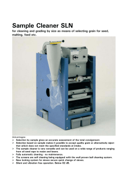
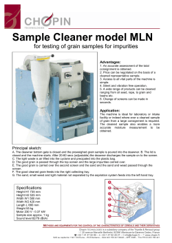
Document 443351
Electronic Supplementary Material (ESI) for Nanoscale.
This journal is © The Royal Society of Chemistry 2014
Supplementary Data 1: Mathematical equations used for modeling
(1) Umklapp phonon-phonon scattering events[1]:
𝑘 𝑇𝜔4
‒1
2 𝐵
𝜏𝑈𝑚𝑘𝑙𝑎𝑝𝑝 = 2𝛾
𝜇𝑉0𝜔𝐷
(1)
where 𝛾 is Gruneisen anharmonicity parameter, μ is shear modulus, V0 is volume per
atom, 𝜔𝐷 is Debye frequency, T is ambient temperature and 𝜔 is phonon angular
frequency.
(2) mass-difference impurity scattering[2]:
‒1
𝜏𝑑𝑒𝑓𝑒𝑐𝑡
=
𝑛𝑉2𝜔4 ∆𝑀
4𝜋𝑣3 𝑀
𝑠
( )
2
(2)
where 𝑣𝑠 is an averaged phonon group velocity, n is the dopant concentration is
denoted, V is the volume of the host (silicon) atom, M is the silicon atomic mass, and
∆𝑀
is the difference between the host and impurity atomic masses.
(3) Phonon to grain boundary scattering[3] :
‒1
𝜏𝑔𝑟𝑎𝑖𝑛
=
where
𝑑𝑔(𝑧)
𝑑
𝑣𝑠
0
𝑔
1 ‒ 𝑝𝑡𝑟
∫𝑑 (𝑧)(1 + 𝑝
𝑡𝑟
)
𝑑𝑧
(3)
is the grain size at thickness z, 𝑝𝑡𝑟 is the probability of specular
transmission (0≤𝑝𝑡𝑟≤1).
(4) Segregated dopants induced scattering[4]:
𝑑
‒1
𝜏𝑠𝑒𝑔𝑟𝑎𝑔𝑎𝑡𝑒𝑑
𝑑𝑜𝑝𝑎𝑛𝑡𝑠
=
∫𝜋𝑑 (𝑧){1 + [
0
2𝑣𝑠
𝜋 2
𝛿(𝜔,𝑧)
2
()
𝑒
𝑔
‒1
]
}
‒1 ‒1
𝑑𝑧
(4)
where 𝛿(𝜔,𝑧) is the grain boundary scattering strength.
Table S1 The parameters used for simulation
Temperature
Doping concentration
(K)
(cm-3)
300
3*1019
Maximum grain
Minimum grain
size
size
(nm)
(nm)
400
100
Supplementary Data 2: Measurement setup of thermal electric properties of
poly-Si
Figure.S1 Testing setup for the measurement of thermoelectric properties of poly-Si.
The measurement is conducted with a probe-station (Cascade Microtech, PMV200)
equipped with a vacuum chamber, which can provide vacuum level at 10-3 mbar, to
eliminate the influence of the thermal conductance due to air. The Chip is clamped
onto a metal chuck, which acts as a large heat sink. The temperature of the chuck is
controlled by a temperature stabilizer to maintain a constant temperature. The output
signal can be readout by the probe and received by a semiconductor parameter
analyzer (Agilent technology, 4156C)
Supplementary Data 3: Characterization results of the test key
Figure.S2 The characterization with input power vs. output voltage of n-type poly-Si
(a) and p-type poly-Si (b) test-key at room temperature.
As shown in this figure, the output is quite linear to the input power which suggests
the contact between the Al and poly-Si is quite good and the temperature rise caused
by the micro-heater do not influence the performance of thermocouple obviously.
[1] Mingo, N. Calculation of Si nanowire thermal conductivity using complete
phonon dispersion relations. Physical Review B, 68(11), 113308(2003).
[2] Zou, J., & Balandin, A. Phonon heat conduction in a semiconductor
nanowire. Journal of Applied Physics, 89(5), 2932-2938(2001).
[3] McConnell, A. D., Uma, S., & Goodson, K. E. Thermal conductivity of doped
polysilicon layers. Microelectromechanical Systems, Journal of, 10(3), 360369(2001)..
[4] Goodson, K. E. Thermal conduction in nonhomogeneous CVD diamond layers in
electronic microstructures. Journal of Heat Transfer,118(2), 279-286(1996).


© Copyright 2026