
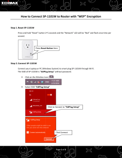
AN-10XX APPLICATION NOTE
AN-10XX APPLICATION NOTE One Technology Way • P.O. Box 9106 • Norwood, MA 02062-9106, U.S.A. • Tel: 781.329.4700 • Fax: 781.461.3113 • www.analog.com AD9832/AD9835 Programming Examples by Liam Riordan INTRODUCTION This application note describes how to load a sinusoidal waveform on the output of the AD9832/AD9835 parts. The commands examined include, setting up the AD9832/5 from a power on scenario, setting up the FSELECT control bit and loading new data to part while using the FSELECT bit control. provide an analog output of fullscale. To avoid spurious DAC outputs while the AD9832 is being initialized, the RESET bit should be set to 1 until the part is ready to begin generating an output. The RESET bit does not reset the phase, frequency, or control registers. These registers will contain invalid data, and therefore should be set to a known value by the user. The RESET bit should then be set to 0 to begin generating an output. The data appears on the DAC output seven to eight MCLK cycles after RESET is set to 0. PROGRAMMING THE AD9832/AD9835 When the AD9832/AD9835is powered up, the part should be reset. This resets appropriate internal registers to zero to FUNCTIONAL BLOCK DIAGRAM DVDD FSELECT BIT FSELECT AVDD AGND REFOUT FS ADJUST REFIN SELSRC ON-BOARD REFERENCE MUX FULL-SCALE CONTROL SYNC FREQ0 REG 12 MUX PHASE ACCUMULATOR (32 BIT) FREQ1 REG SIN ROM 10-BIT DAC COMP IOUT PHASE0 REG PHASE1 REG AD9832 MUX PHASE2 REG SYNC PHASE3 REG SYNC 16-BIT DATA REGISTER SYNC 8 MSBs 8 LSBs DEFER REGISTER SELSRC CONTROL REGISTER DECODE LOGIC FSELECT/PSEL REGISTER MUX PSEL0 BIT MUX PSEL1 BIT SERIAL REGISTER FSYNC SCLK PSEL0 PSEL1 SDATA Figure 1.AD9832 Functional Block Diagram Rev. 0 | Page 1 of 5 09090-001 MCLK DGND AN-10XX Application Note TABLE OF CONTENTS Introduction ...................................................................................... 1 Functional Block Diagram ...............................................................1 Programming the AD9832/AD9835 .............................................. 1 Programming the AD9832/AD9835...............................................3 Rev. 0 | Page 2 of 5 Application Note AN-10XXXX PROGRAMMING THE AD9832/AD9835 Command Sequence Explained A simple example is the best method to explain how to program the AD9832/ AD9835. For further details refer to the apps note AN-621 & the AD9832 or the AD9835 datasheet. Please refer to the register tables in the AD9832/35 datasheet for reference. Example 1: Setting Up Part After Power-Up 0xD000—Resets AD9832. The aim is to generate a 2 output frequencies, loading 3 KHz to Freq0 register and 10 KHz to Freq1 register, with a 25 MHz MCLK The dial-up code for this is defined by the equation: FreqReg f OUT 2 28 f MCLK RESET bit D12 is set to 1. This resets internal registers to 0, which corresponds to an analog output of fullscale. See Figure 2, Ch1 is the spurious output set to reset.Ch2 is FSYNC, Ch3 is SDIN and Ch4 is SCLK. Note data is valid on falling edge of SCLK. Please ignore the SDIN high after 8 SCLK cycles – this is an inherent feature of the particular SPI driver used and does not affect the part. For Freq0 = 3000 Hz. Freq0 3000 Hz 2 32 25 MHz = 515396 decimal = 0x0007DD44 For Freq1 = 10KHz 10000 Hz 232 Freq1 25 MHz = 1717987 decimal = 0x001A363E See ADIsimDDS tool for a quick and easy method of generating the desired code in hex, decimal or binary. http://designtools.analog.com/dtDDSWeb/dtDDSMain.aspx Figure 2. Put AD9832/35 in Reset – 0xD000 0x3044 The required initialization sequence is shown in Table 1. 8-bits to Defer. Table 1. Initialisation Sequence Frequency Register 0 L LSB data. 8-bit data = 0x44 Hexadecimal 0xD000 0x3044 0x21DD 0x3207 0x2300 0x343E 0x2536 0x361A 0x2700 0x9000 0XC000 Binary 1101 0000 0000 0000 0011 0000 0100 0100 0010 0001 1101 1101 0011 0010 0000 0111 0010 0011 0000 0000 0011 0100 0011 1110 0010 0101 0011 0110 0011 0110 0001 1010 0010 0111 0000 0000 1001 0000 0000 0000 1100 0000 0000 0000 0x21DD Rev. 0 | Page 3 of 5 Present 8 bits + deferred 8 bits to select Frequency Register. Frequency Register 0 H LSB data 8-bit data (0xDD) + deferred data = 0xDD44 AN-10XX Application Note Example 2: Changing FSELECT Bit The part is now setup with a 3KHz signal on the output and the part is controllablke by the FSELECT bit, as opposed to FSELECT pin. To change this frequency to 10KHz all that is required is a write to the control register to change the FSELECT bit. 0x5800 — Selects FREQ1 register. That’s 0x5 written to the Command bits C3-C0. a 1 written to bit D11 to select the FREQ1 register – see Figure 5. To return to the 3KHz Freq0 output reset FSELECT bit to 0 -load 0x5000 again. Figure 3. Load 0x21DD 0x3207—Frequency Register 0 L MSB data 0x2300—Frequency Register 0 H MSB data 0x343E—Frequency Register 1 L LSB data. 0x2536—Frequency Register 1 H LSB data. 0x361A—Frequency Register 1 L MSB data. 0x2700—Frequency Register 1 H MSB data. 0x9000—Set SELSRC to 1 using Command bits 1,0 for C15,C14. Setting SELSRC to 1 – FSELECT is controlled by data bits. Latency increased by 2 MCLK cycles. 0xC000—Frequency Register 1 L LSB data. Exit reset mode. A 3 KHz signal, from FREQ0 register, appears at the output of the DAC eight MCLK cycles after RESET bit is set to zero. Figure 5. Change FSELECT bit – 0x5800 Example 3: Updating the output “on the fly”. The next step is to change the FREQ1 register from 10KHz to 40KHz without entering RESET mode. For Freq1 = 40KHz Freq1 40000 Hz 232 25 MHz = 6871948 decimal = 0x0068DB8C Load the following command sequence: 0x348C—Frequency Register 1 L LSB data. 0x25DB—Frequency Register 1 H LSB data. 0x3668—Frequency Register 1 L MSB data. Figure 4. Take Part Out Of Reset – 0xC000 0x2700—Frequency Register 1 H MSB data. 0x9000 —Latch to output by synchonising data. In this case the SELSRC bit was again set to 1 using Command bits 1,0 for C15,C14. Basically the part simply needs to see a falling FSYNC edge to latch data, seeFigure 6. Rev. 0 | Page 4 of 5 Application Note AN-10XXXX Figure 6. Changing FREQ1 Output from 10KHz to 40KHz ©2010 Analog Devices, Inc. All rights reserved. Trademarks and registered trademarks are the property of their respective owners. AN08955-0-3/10(0) Rev. 0 | Page 5 of 5


© Copyright 2026